KR101284921B1 - electrophoretic display device and manufacturing method thereof - Google Patents
electrophoretic display device and manufacturing method thereofDownload PDFInfo
- Publication number
- KR101284921B1 KR101284921B1KR1020060042795AKR20060042795AKR101284921B1KR 101284921 B1KR101284921 B1KR 101284921B1KR 1020060042795 AKR1020060042795 AKR 1020060042795AKR 20060042795 AKR20060042795 AKR 20060042795AKR 101284921 B1KR101284921 B1KR 101284921B1
- Authority
- KR
- South Korea
- Prior art keywords
- electrode
- line
- display device
- common
- gate
- Prior art date
- Legal status (The legal status is an assumption and is not a legal conclusion. Google has not performed a legal analysis and makes no representation as to the accuracy of the status listed.)
- Expired - Fee Related
Links
Images


Classifications
- G—PHYSICS
- G02—OPTICS
- G02F—OPTICAL DEVICES OR ARRANGEMENTS FOR THE CONTROL OF LIGHT BY MODIFICATION OF THE OPTICAL PROPERTIES OF THE MEDIA OF THE ELEMENTS INVOLVED THEREIN; NON-LINEAR OPTICS; FREQUENCY-CHANGING OF LIGHT; OPTICAL LOGIC ELEMENTS; OPTICAL ANALOGUE/DIGITAL CONVERTERS
- G02F1/00—Devices or arrangements for the control of the intensity, colour, phase, polarisation or direction of light arriving from an independent light source, e.g. switching, gating or modulating; Non-linear optics
- G02F1/01—Devices or arrangements for the control of the intensity, colour, phase, polarisation or direction of light arriving from an independent light source, e.g. switching, gating or modulating; Non-linear optics for the control of the intensity, phase, polarisation or colour
- G02F1/165—Devices or arrangements for the control of the intensity, colour, phase, polarisation or direction of light arriving from an independent light source, e.g. switching, gating or modulating; Non-linear optics for the control of the intensity, phase, polarisation or colour based on translational movement of particles in a fluid under the influence of an applied field
- G02F1/166—Devices or arrangements for the control of the intensity, colour, phase, polarisation or direction of light arriving from an independent light source, e.g. switching, gating or modulating; Non-linear optics for the control of the intensity, phase, polarisation or colour based on translational movement of particles in a fluid under the influence of an applied field characterised by the electro-optical or magneto-optical effect
- G02F1/167—Devices or arrangements for the control of the intensity, colour, phase, polarisation or direction of light arriving from an independent light source, e.g. switching, gating or modulating; Non-linear optics for the control of the intensity, phase, polarisation or colour based on translational movement of particles in a fluid under the influence of an applied field characterised by the electro-optical or magneto-optical effect by electrophoresis
- G—PHYSICS
- G02—OPTICS
- G02F—OPTICAL DEVICES OR ARRANGEMENTS FOR THE CONTROL OF LIGHT BY MODIFICATION OF THE OPTICAL PROPERTIES OF THE MEDIA OF THE ELEMENTS INVOLVED THEREIN; NON-LINEAR OPTICS; FREQUENCY-CHANGING OF LIGHT; OPTICAL LOGIC ELEMENTS; OPTICAL ANALOGUE/DIGITAL CONVERTERS
- G02F1/00—Devices or arrangements for the control of the intensity, colour, phase, polarisation or direction of light arriving from an independent light source, e.g. switching, gating or modulating; Non-linear optics
- G02F1/01—Devices or arrangements for the control of the intensity, colour, phase, polarisation or direction of light arriving from an independent light source, e.g. switching, gating or modulating; Non-linear optics for the control of the intensity, phase, polarisation or colour
- G02F1/13—Devices or arrangements for the control of the intensity, colour, phase, polarisation or direction of light arriving from an independent light source, e.g. switching, gating or modulating; Non-linear optics for the control of the intensity, phase, polarisation or colour based on liquid crystals, e.g. single liquid crystal display cells
- G02F1/133—Constructional arrangements; Operation of liquid crystal cells; Circuit arrangements
- G02F1/136—Liquid crystal cells structurally associated with a semi-conducting layer or substrate, e.g. cells forming part of an integrated circuit
- G—PHYSICS
- G02—OPTICS
- G02F—OPTICAL DEVICES OR ARRANGEMENTS FOR THE CONTROL OF LIGHT BY MODIFICATION OF THE OPTICAL PROPERTIES OF THE MEDIA OF THE ELEMENTS INVOLVED THEREIN; NON-LINEAR OPTICS; FREQUENCY-CHANGING OF LIGHT; OPTICAL LOGIC ELEMENTS; OPTICAL ANALOGUE/DIGITAL CONVERTERS
- G02F1/00—Devices or arrangements for the control of the intensity, colour, phase, polarisation or direction of light arriving from an independent light source, e.g. switching, gating or modulating; Non-linear optics
- G02F1/35—Non-linear optics
- G02F1/355—Non-linear optics characterised by the materials used
- G02F1/361—Organic materials
Landscapes
- Physics & Mathematics (AREA)
- Nonlinear Science (AREA)
- Optics & Photonics (AREA)
- General Physics & Mathematics (AREA)
- Chemical & Material Sciences (AREA)
- Mathematical Physics (AREA)
- Crystallography & Structural Chemistry (AREA)
- Engineering & Computer Science (AREA)
- Microelectronics & Electronic Packaging (AREA)
- Health & Medical Sciences (AREA)
- Life Sciences & Earth Sciences (AREA)
- Chemical Kinetics & Catalysis (AREA)
- Electrochemistry (AREA)
- Molecular Biology (AREA)
- Electrochromic Elements, Electrophoresis, Or Variable Reflection Or Absorption Elements (AREA)
Abstract
Translated fromKoreanDescription
Translated fromKorean도 1a는 종래의 전기영동 표시장치의 평면도.1A is a plan view of a conventional electrophoretic display.
도 1b는 도 1a의 I-I'에 따른 단면도.1B is a sectional view taken along line II ′ of FIG. 1A;
도 2는 종래의 전기영동 표시장치의 배면을 도시한 도면.Figure 2 is a view showing the back of the conventional electrophoretic display device.
도 3a는 본 발명에 따른 전기영동 표시장치의 평면도.3A is a plan view of an electrophoretic display device according to the present invention;
도 3b는 도 3a의 Ⅱ-Ⅱ'에 따른 단면도.FIG. 3B is a cross-sectional view taken along line II-II 'of FIG. 3A;
도 4는 본 발명에 따른 전기영동 표시장치의 잉크층을 도시한 도면.4 illustrates an ink layer of an electrophoretic display device according to the present invention.
도 5a는 본 발명에 따른 전기영동 표시장치의 전면표시부를 도시한 도면.5A illustrates a front display of an electrophoretic display device according to the present invention;
도 5b는 본 발명에 따른 전기영동 표시장치의 후면표시부를 도시한 도면.Figure 5b is a view showing a rear display of the electrophoretic display device according to the present invention.
도 6a 내지 도 6d는 본 발명에 따른 전기영동표시장치의 드라이버층을 형성하는 공정도.6A through 6D are process diagrams for forming a driver layer of the electrophoretic display device according to the present invention;
(도면의 주요 부분에 대한 부호의 설명) (Explanation of symbols for the main parts of the drawing)
1 : 전기영동 표시장치 3 : 잉크층 1
5 : 드라이버층 7 : 화소셀 5
10 : 기판 20 : 공통전극 10: substrate 20: common electrode
30 : 게이트라인 32 : 게이트전극 30: gate line 32: gate electrode
35 : 공통라인 40 : 게이트절연막 35
50 : 반도체층 60 : 데이터라인 50: semiconductor layer 60: data line
70 : 패시베이션막 80 : 제1전극 70
110 : 대전입자120 : 제2전극110: charged particle 120: second electrode
본 발명은 표시장치에 관한 것으로서, 더욱 구체적으로 전기영동 표시장치에 관한 것이다.The present invention relates to a display device, and more particularly to an electrophoretic display device.
오늘날 많은 정보량을 휴대할 수 있으며, 다수의 정보를 전달할 수 있는 개인용 컴퓨터 등과 같은 디스플레이 장치로 신문이나 잡지 등의 기사를 읽을 수 있음에도 불구하고 빠른속도로 진행되는 정보화 사회에 어울리지 않게 휴대할 수 있는 정보량이 얼마 안되는 신문, 잡지와 같은 종이라는 매체에 의해서 정보가 전달되고 있다.Today, a large amount of information can be carried, and a display device such as a personal computer that can convey a large amount of information can read articles such as newspapers and magazines, but the amount of information that can be carried in a fast paced information society Information is transmitted by a medium such as a few newspapers and magazines.
이와 같이, 상기 신문, 잡지 등이 사라지지 않는 이유는 상기 디스플레이 장치를 사용하기 위해서 상기 디스플레이 장치의 전원을 켜고 잠시 기다려야 하고 상기 신문과 잡지 등을 읽기 위해 장시간 한 화면을 유지하기 위한 소비전력이 크다는 단점이 있다. As such, the reason why the newspapers and magazines do not disappear is that power to maintain a screen for a long time to turn on the display device and wait for a while to use the display device and to read the newspapers and magazines is large. There are disadvantages.
그래서 상기 디스플레이 장치의 단점을 해결하고 신문, 잡지 등의 내용을 표시할 수 있는 디스플레이 장치를 필요로 하게 된다. 이와 같이, 상기 디스플레이 장치에 의해 구현될 수 있는 것이 전자종이(E-Paper)이다.Therefore, there is a need for a display device capable of solving the disadvantages of the display device and displaying contents such as newspapers and magazines. As such, the electronic paper may be implemented by the display device.
상기 전자종이는 박형의 두께로 형성할 수 있으며, 전기적인 수단으로 데이터의 표시, 삭제가 가능한 디스플레이이다. 즉, 텍스트와 이미지를 표현할 수 있는 전자종이는 전통적인 인쇄매체가 가지는 특징과 비디오 화면이 가지는 특징이 결합되어 신속한 정보를 전달할 수 있는 매체가 될 것으로 전망되고 있다.The electronic paper may be formed in a thin thickness and is a display capable of displaying and deleting data by electrical means. In other words, electronic paper capable of expressing text and images is expected to be a medium that can deliver information quickly by combining features of traditional print media and features of video screens.
또한, 상기 전자종이는 액정표시장치에서는 취약한 높은 시인성 및 간편성 등이 강조되면서 새로운 표시장치로써 부각 받고 있다.In addition, the electronic paper has been highlighted as a new display device with emphasis on high visibility and simplicity, which is weak in a liquid crystal display device.
상기 전자종이를 구현할 수 있는 방법으로는 대전 비즈(bead)를 사용하는 방법, 전기영동으로 대전입자를 구동하여 표시하는 방법 등이 있다.The electronic paper may be implemented by using a charging bead, a method of driving a charged particle by electrophoresis, and the like.
일실시예로써 전기영동으로 대전입자를 구동하는 방법을 설명하며, 상기 방법으로 구동되는 표시장치를 전기영동 표시장치로 칭한다.As an embodiment, a method of driving charged particles by electrophoresis will be described, and a display device driven by the above method will be referred to as an electrophoretic display device.
상기 전기영동 표시장치는 기존의 평판표시장치에 비해, 전원을 꺼도 화면이 사라지지 않는 특성을 가진다. 이로써, 상기 전기영동 표시장치는 화면을 바꾸고자 할 때만 전원을 가하면 되기 때문에 저소비전력이면서 기존 종이와 같은 특성을 확보할 수 있다는 장점이 있다.The electrophoretic display has a characteristic that the screen does not disappear even when the power is turned off, compared to the conventional flat panel display. As a result, the electrophoretic display needs to apply power only to change the screen, thereby achieving low power consumption and securing the same characteristics as conventional paper.
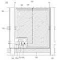
도 1a 및 도 1b는 종래의 전기영동 표시장치를 설명하기 위해 도시한 도면이다. 도 1a는 종래의 전기영동 표시장치를 도시한 평면도이고, 도 1b는 도 1a의 I-I'에 따른 단면도이다.1A and 1B are diagrams for describing a conventional electrophoretic display device. 1A is a plan view illustrating a conventional electrophoretic display, and FIG. 1B is a cross-sectional view taken along line II ′ of FIG. 1A.
도 1a 및 도 1b를 참조하면, 전기영동 표시장치(501)는 기판(510)상에 다수의 게이트라인(530)과 데이터라인(560)이 서로 교차되어 배치된다. 이때, 상기 게 이트라인(530)과 상기 데이터라인(560)에 의해 구획되는 영역을 화소셀(Cell: 507) 영역으로 정의한다.1A and 1B, in the
또한, 상기 전기영동 표시장치(501)는 상기 게이트라인(530)과 평행방향으로 형성되며, 일정간격으로 이격되어 배치된 공통라인(520)이 위치한다.In addition, the
여기서, 상기 화소셀(507) 영역 내에 상기 공통라인(520)에 연결된 공통전극(525)이 형성된다. 상기 공통전극(525)은 화소셀(507) 영역의 소정면적 차지하며, 상기 공통전극(525) 상에 형성되는 금속과 오버랩되어 전기영동 표시장치(501)의 표시전압 유지용량을 형성하도록 하는 역할을 한다.Here, a
그리고 상기 게이트라인(530)과 데이터라인(560)의 교차 영역에는 박막트랜지스터(TR)가 형성된다. 즉, 상기 박막트랜지스터(TR)은 게이트전극(532), 반도체층(550), 소스/드레인전극(560a, 560b)을 포함한다.A thin film transistor TR is formed at an intersection of the
자세히 설명하면, 상기 게이트라인(530) 상에는 게이트절연막(540)이 형성되고 상기 게이트절연막(540) 상에는 데이터라인(560)이 형성된다. 여기서, 상기 데이터라인(560)에는 소스전극(560a)이 연결되어 있으며, 상기 드레인전극(560b)은 상기 반도체층(550)을 사이에 두고 상기 소스전극(560a)에 소정간격 이격되어 형성된다. 그리고 상기 데이터라인(560) 상에는 패시베이션막(570)이 형성된다.In detail, a
여기서 상기 드레인전극(560b)에는 화소셀(507) 영역까지 연장되어 캐패시터 역할을 하는 드레인부(565)가 형성된다. 즉, 상기 드레인부(565)는 하부에 있는 상기 공통전극(525)과 중첩되어 형성된다.The
상기 전기영동 표시장치(501)는 하나의 화상을 오랫동안 유지해야 하는 전자 종이인 경우에, 상기 전압 보전율의 특성이 중요하다. 여기서, 상기 전압 보전율은 신호전압이 인가된 뒤, 다음 신호전압이 인가될 때까지 전압을 유지함에 있어, 상기 전압을 유지하는 유지율을 의미한다.In the case where the
이 때, 상기 전기영동장치(501)가 상기 전압 보전율 특성을 유지하기 위해서는 큰 캐패시던스가 필요하게 된다. 그래서 상기 전기영동 표시장치(501)는 불투명한 금속막으로 형성된 상기 공통전극(525)과 불투명한 상기 드레인부(565)의 중첩영역을 크게 형성하게 된다.At this time, in order for the
이와 같이, 상기 드레인부(565)와 상기 공통전극(525)이 오버랩됨에 따라 전기영동 표시장치(501)는 표시전압 유지용량을 가지게 되어 표시화면을 유지할 수 있게 된다.As described above, as the
즉, 재기록의 전기신호를 보내지 않는 한 한번 표시된 내용은 전기를 소비하지 않고 그대로 표시화면을 유지하게 된다. 따라서 상기 전기영동 표시장치(501)는 소비전력이 낮은 장점을 갖게 된다.That is, unless the electric signal for rewriting is sent, the content displayed once does not consume electricity and maintains the display screen as it is. Therefore, the
상기 소스/드레인전극(560a, 560b), 드레인부(565), 데이터라인(560) 등과 박막트랜지스터(TR) 상에는 상기 라인들 및 박막트랜지스터를 보호하는 패시베이션막(570)이 형성된다.A
상기 패시베이션막(570)에는 패시홀(575)이 형성되어 상기 드레인전극(560b)을 일부분 노출시키게 된다.A passivation hole 575 is formed in the
여기서 상기 패시베이션막(570) 상에는 상기 드레인전극(560b)과 전기적으로 연결되는 제1전극(580)이 형성된다. 상기 제1전극(580)은 상기 화소셀(507) 영역과 상기 게이트라인(530), 데이터라인(560)을 포함하도록 형성된다.In this case, a
한편, 도시하지 않았지만 상기 제1전극(580)상에는 다수의 대전입자를 갖는 캡술 및 일정전압이 인가되는 제2전극을 구비한 잉크층이 마련된다.Although not shown, an ink layer having a capsul having a plurality of charged particles and a second electrode to which a predetermined voltage is applied is provided on the
여기서, 상기 잉크층에 마련된 다수의 대전입자는 전계에 의해 이동하게 된다. 여기서 상기 대전입자는 화이트색으로는 산화타이탄륨(TiO2), 블랙색으로는 카본 블랙(Carbon-Black)을 사용할 수 있다.Here, the plurality of charged particles provided in the ink layer is moved by the electric field. Here, the charged particles may use titanium oxide (TiO2 ) as the white color and carbon black (Carbon-Black) as the black color.
이와 같이, 상기 전기영동 표시장치(501)는 상기 제1전극(580)과 상기 제2전극에 형성되는 전계에 의해, 상기 잉크층에 구비되는 대전입자를 이동시켜 화상을 표시할 수 있게 된다.As described above, the
이 때, 상기 전기영동 표시장치(501)는 액정표시장치와 같이 편광된 빛에 의해 영상을 표시하는 방식이 아니기 때문에 시야각이 넓은 장점을 가질 수 있다.In this case, the
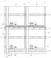
도 2는 종래의 전기영동 표시장치의 배면을 도시한 도면이다.2 is a diagram illustrating a rear surface of a conventional electrophoretic display device.
도 2에 도시된 바와 같이, 전기영동 표시장치(501)는 스위칭소자(TR) 및 전기신호를 연결해 주는 다수의 라인(530, 560)이 불투명한 금속으로 마련되어 있다.As shown in FIG. 2, the
상기 라인은 기판 면에 가로 방향으로 형성되는 게이트라인(530)과 세로 방향으로 형성되는 데이터라인(560)에 의해서 구획되어 정의되는 화소셀(507)이 형성된다.The line is formed on the substrate surface by a
기판 면에는 불투명한 게이트전극(532)과 일체인 상기 게이트라인(530)이 소정간격 이격되어 형성된다. 그리고 상기 게이트라인(530)과 동일한 불투명한 금속 등으로 화소셀(507) 영역에 공통전극(525)이 형성된다. 여기서 공통전극(525)은 공통라인(520)으로 연결되어 있다.The
그리고 상기 게이트라인(530)과 직교하는 방향으로 데이터라인(560)을 형성한다. 여기서 상기 데이터라인(560)은 불투명한 금속으로 형성한다. 여기서 상기 데이터라인(560)과 일체인 소스전극(560a), 상기 소스전극(560a)과 소정간격 이격된 드레인전극(560b)이 기판 전면에 형성된다.The
게다가 상기 전기영동 표시장치(501)는 표시전압 유지용량을 유지하기 위해 캐패시터 역할을 하는 드레인부(565)가 상기 드레인전극(565)에서 연장되어 화소셀(507) 영역에 큰 면적을 차지하며 형성되어 있다.In addition, the
여기서 상기 드레인부(565)는 상기 데이터라인(560)과 동일 금속으로 형성되어 불투명한 금속으로 형성된다.The
이와 같이, 상기 전기영동 표시장치(501)에는 캐패시터 역할을 하며, 불투명금속으로 형성되는 드레인부(565) 및 공통전극(525)이 화소셀(507) 영역에 큰 면적으로 형성되어 있기 때문에 상기 전기영동 표시장치(501)의 배면 방향에는 불투명한 금속으로 가려져 영상을 선명하게 볼수 없는 단점이 있다.As described above, the
따라서, 상기 전기영동 표시장치(501)는 불투명한 다수의 라인(530, 560), 불투명한 드레인부(565), 공통전극(525)에 의해서 표시방향이 한정되어 있다.Accordingly, the display direction of the
본 발명은 전압보전율을 유지시키면서 양방향으로 화면을 표시할 수 있는 표 시장치를 제공함에 그 목적이 있다.It is an object of the present invention to provide a table market value capable of displaying a screen in both directions while maintaining the voltage holding ratio.
상기 기술적 과제를 이루기 위하여 본 발명의 전기영동 표시장치는 다수의 게이트라인과 다수의 데이터라인으로 구획되어 정의되는 다수의 화소셀을 구비한 기판과; 상기 화소셀의 소정면적에 형성되며, 상기 기판 상에 투명전도성 물질로 형성되는 공통전극과; 상기 게이트라인과 상기 데이터라인이 교차하는 영역에 형성되는 스위칭소자와; 상기 기판 전면에 형성되어 상기 스위칭소자를 보호하며, 콘택홀을 구비한 패시베이션막과; 상기 콘택홀을 통해서 상기 스위칭소자와 연결되며, 상기 패시베이션막 상에 상기 공통전극과 중첩되도록 상기 화소셀 영역에 투명전도성 물질로 형성되는 제1전극과; 상기 제1전극 상에 일정전압이 인가되는 제2전극 및 전하를 갖는 다수의 대전입자를 구비한 잉크층을 포함하는 것을 특징으로 한다.According to an aspect of the present invention, there is provided an electrophoretic display device including: a substrate having a plurality of pixel cells defined by a plurality of gate lines and a plurality of data lines; A common electrode formed on a predetermined area of the pixel cell and formed of a transparent conductive material on the substrate; A switching element formed in an area where the gate line and the data line cross each other; A passivation film formed over the substrate and protecting the switching device, the passivation film including a contact hole; A first electrode connected to the switching element through the contact hole and formed of a transparent conductive material in the pixel cell region so as to overlap the common electrode on the passivation layer; And an ink layer including a second electrode to which a predetermined voltage is applied and a plurality of charged particles having a charge on the first electrode.
그리고 상기 공통전극은 ITO 또는 IZO를 포함하는 투명전도성 물질로 형성되는 것을 특징으로 한다.The common electrode may be formed of a transparent conductive material including ITO or IZO.
여기서 전기영동 표시장치는 상기 대전입자의 이동으로 전면표시부에 이미지가 표시되며, 상기 후면표시부에는 투명전도성 물질로 형성된 상기 제1전극, 상기 제2전극 및 상기 공통전극으로 투과이미지가 표시되는 것을 특징으로 한다.In this case, the electrophoretic display device displays an image on a front display part by moving the charged particles, and transmits an image on the rear display part by the first electrode, the second electrode, and the common electrode formed of a transparent conductive material. It is done.
상기 기술적 과제를 이루기 위하여 본 발명에 따른 전기영동 표시장치 제조방법은 기판 상에 투명전도성 물질로 공통전극을 형성하는 단계; 상기 기판 상에 게이트 금속물질로 게이트라인 및 상기 게이트라인에 평행하며, 상기 공통전극과 연결되는 공통라인을 형성하는 단계; 상기 기판 전면에 게이트라인 및 상기 공통라인을 절연하는 게이트 절연막을 형성하는 단계; 상기 게이트절연막 상에 형성되며, 상기 게이트라인에서 돌출되어 형성된 게이트전극 상에 반도체층을 형성하는 단계; 상기 반도체층 상에 일부분 중첩되게 형성되는 소스/드레인전극 및 상기 게이트라인에 교차하도록 데이터라인을 형성하는 단계; 상기 데이터라인이 형성된 기판 전면에 형성되며, 다수의 콘택홀을 구비하는 패시베이션막을 형성하는 단계; 상기 콘택홀을 통해 상기 드레인전극에 연결되며, 상기 패시베이션막 상에 제1전극을 형성하는 단계; 상기 제1전극 상에 일정전압이 인가되는 제2전극 및 전하를 갖는 다수의 대전입자를 구비한 잉크층을 형성하는 단계를 포함하는 것을 특징으로 한다.According to an aspect of the present invention, there is provided a method of manufacturing an electrophoretic display device, the method including: forming a common electrode of a transparent conductive material on a substrate; Forming a common line on the substrate, the common line being parallel to the gate line and the gate line with a gate metal material, and connected to the common electrode; Forming a gate insulating film insulating the gate line and the common line in front of the substrate; Forming a semiconductor layer on the gate insulating layer, the semiconductor layer protruding from the gate line; Forming a data line to intersect the gate line and the source / drain electrode partially overlapping the semiconductor layer; Forming a passivation film formed on an entire surface of the substrate on which the data line is formed and having a plurality of contact holes; Forming a first electrode on the passivation layer, the first electrode being connected to the drain electrode through the contact hole; And forming an ink layer including a second electrode to which a predetermined voltage is applied and a plurality of charged particles having charges on the first electrode.
이하, 본 발명에 의한 전기 영동 표시 장치의 도면을 참고하여 상세하게 설명한다. 다음에 소개되는 실시예들은 당업자에게 본 발명의 사상이 충분히 전달될 수 있도록 하기 위해 예로서 제공되어지는 것이다. 따라서, 본 발명은 이하 설명되어지는 실시예들에 한정되지 않고 다른 형태로 구체화될 수도 있다. 그리고, 도면들에 있어서, 장치의 크기 및 두께 등은 편의를 위하여 과장되어 표현될 수도 있다. 명세서 전체에 걸쳐서 동일한 참조번호들은 동일한 구성요소들을 나타낸다.Hereinafter, with reference to the drawings of the electrophoretic display device according to the present invention will be described in detail. The following embodiments are provided by way of example so that those skilled in the art can fully understand the spirit of the present invention. Therefore, the present invention is not limited to the embodiments described below, but may be embodied in other forms. In the drawings, the size and thickness of an apparatus may be exaggerated for convenience. Like numbers refer to like elements throughout.
본 발명은 전기영동법으로 전자종이를 구성하는 표시장치를 실시예로 설명한다.The present invention describes a display device constituting electronic paper by electrophoresis according to an embodiment.
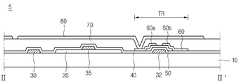
도 3a 및 도 3b는 본 발명의 따른 전기영동 표시장치의 드라이버층을 설명하기 위해 도시한 도면들이고, 도 4는 본 발명에 따른 전기영동 표시장치의 잉크층을 도시한 도면이다. 여기서, 도 3a는 본 발명에 따른 전기영동 표시장치의 평면도이 고, 도 3b는 도 3a의 Ⅱ-Ⅱ'에 따른 단면도이다.3A and 3B are views for explaining a driver layer of an electrophoretic display device according to the present invention, and FIG. 4 is a view showing an ink layer of the electrophoretic display device according to the present invention. 3A is a plan view of an electrophoretic display device according to the present invention, and FIG. 3B is a cross-sectional view taken along line II-II 'of FIG. 3A.
도 3a 및 도 3b를 참조하여 설명하면, 본 발명에 따른 전기영동 표시장치(1)는 다수의 대전입자(참조 도 4 의 110)를 구비하는 잉크층(참조 도 4의 3)과 상기 대전입자(110)를 구동할 수 있는 드라이버층(5)을 구비하고 있다.Referring to FIGS. 3A and 3B, the
상기 드라이버층(5)은 다수의 화소셀(7)을 구비하는 기판(10)이 마련된다. 상기 기판(10)은 유리, 플라스틱, 스테인레스 포일 중 어느 하나일 수 있다.The
상기 기판(10)상에는 게이트라인(30)과 데이터라인(60)이 서로 교차하도록 배치되며 상기 게이트라인(30)과 데이터라인(60)에 구획되는 영역에 화소셀(7)이 정의된다.The
상기 화소셀(7)에는 소정 면적으로 형성되며 투명전도성 물질로 형성된 공통전극(20)이 형성된다. 여기서 상기 투명전도성 물질은 ITO, IZO 등을 사용할 수 있다.The
여기서 상기 공통전극(20)은 화소셀(7) 영역에 소정면적으로 형성되는데, 상기 전기영동 표시장치(1)는 추후에 설명할 제1전극(80) 상에 필름형상의 잉크층(3)이 마련되며 상기 잉크층(3)은 저항이 낮아 누설전류(Leakage current)가 발생할 수 있게 된다. 즉, 상기 전기영동 표시장치(1)의 화면유지를 위한 충전전압이 자연방전되어 화면이 깜박거리는 현상이 발생할 수 있다. 그래서 상기 공통전극(20)은 화소셀(7) 영역에 큰 면적으로 형성되는 것이 바람직하다.The
그리고 공통라인(35)은 상기 게이트라인(30)과 평행한 방향으로 일정간격 이격되어 상기 기판(10) 상에 형성된다. 여기서 상기 공통라인(35)은 상기 투명전도 성 물질로 형성된 공통전극(20) 상에 마련되어 상기 공통전극(20)은 상기 공통라인(35)에 전기적으로 연결할 수 있게 된다.The
여기서 상기 게이트라인(30)과 상기 공통라인(35)은 게이트 금속물질로 동시에 형성할 수 있다. 상기 공통전극(20)은 잉크층(3)에 구비되어 있는 제2전극(120)에 연결되어 상기 제2전극(120)에 일정전압을 인가하게 된다.The
그리고 상기 공통라인(35), 공통전극(20) 및 게이트라인(30)을 절연하는 게이트절연막(40)이 상기 기판(10) 전면에 형성된다. 여기서, 상기 게이트절연막(40)은 산화실리콘막, 질화실리콘막 또는 이들의 적층막일 수 있다.In addition, a
한편, 상기 게이트라인(30)과 상기 데이터라인(60)의 교차영역에 적어도 하나의 스위칭소자(Tr)가 형성된다.Meanwhile, at least one switching device Tr is formed at an intersection area of the
상기 스위칭소자(TR)는 상기 게이트라인(30)에 일체로 형성된 게이트전극(32)상에 형성된다. 여기서 상기 게이트전극(32)은 상기 게이트라인(30)의 일부분에서 돌기된 형상을 가진다.The switching element TR is formed on the
그리고, 상기 게이트전극(32)과 대응된 상기 게이트절연막(40)상에는 반도체층(50)이 형성된다. 여기서, 상기 반도체층(50)은 비정질 실리콘과, 불순물이 도핑된 비정질 실리콘이 순차적으로 적층되어 각각 형성되는 채널층과 오믹콘택층으로 이루어질 수 있으며, 유기물질로 상기 반도체층(50)을 형성하여 플렉서블(Flexible)한 표시장치를 형성할 수도 있다.The
상기 반도체층(50)의 양단부에는 각각 소스/드레인 전극(60a, 60b)이 형성된다. 여기서, 상기 소스전극(60a)은 상기 데이터라인(60)의 일부분이 돌기된 형상으 로, 상기 데이터라인(60)과 일체로 되어 있다. 그리고 상기 드레인전극(60b)은 상기 반도체층(50)을 사이에 두고 소정간격 이격되어 형성된다.Source /
상기 스위칭소자(Tr) 및 상기 데이터라인(60)이 형성된 상기 게이트절연막(40)상에 패시베이션막(70)이 마련된다. 여기서, 상기 패시베이션막(70)은 BCB, 아크릴계 수지 또는 실리콘계수지로 이루어질 수 있다. 이때, 상기 패시베이션막(70)은 상기 드레인전극(60b)의 일부분을 노출하는 콘택홀(75)이 구비된다.The
상기 패시베이션막(70) 상에는 제1전극(80)이 형성된다. 상기 제1전극(80)은 잉크층(3)에 마련되어 있는 대전입자(110)를 구동시킬 수 있다. 그리고 상기 제1전극(80)은 상기 콘택홀(75)을 통해 상기 드레인전극(60b)과 전기적으로 연결된다.The
여기서 상기 제1전극(80)은 화소셀(7) 영역과 상기 게이트라인(30), 데이터라인(60)의 소정영역까지 오버랩되도록 형성할 수 있다.The
이와 같이 상기 제1전극(80)은 게이트라인(30), 데이터라인(60) 및 상기 공통전극(20), 공통라인(35)과 중첩되도록 형성되어 있다. 이로써, 상기 공통전극(20), 공통라인(35)에 오버랩되는 제1전극(80) 면적이 크게 형성되기 때문에 상기 드라이버층(5)의 캐패시던스가 크게 형성된다. 즉, 상기 전기영동 표시장치(1)의 표시화면을 유지하는 충전전압을 확보할 수 있게 된다.As such, the
여기서 상기 제1전극(80)은 상기 게이트라인(30), 데이터라인(60) 영역까지 형성하게 된다. 이는 상기 잉크층(3)에 구비되는 대전입자(110)들이 상기 게이트라인(30), 데이터라인(60)에 인가되는 전압에 의해서 반응하는 경우가 발생할 수 있다. 이에 따라 상기 대전입자(110)를 통제할 수 없는 경우가 발생할 수 있기 때문 에 상기 제1전극(80)을 상기 게이트라인(30), 데이터라인(60) 영역까지 형성하게 된다.In this case, the
이와 같이 상기 드라이버층(5)에는 상기 제1전극(80)을 스위칭할 수 있는 스위칭소자(TR)와 상기 화면유지를 위한 충전전압을 형성할 수 있는 공통전극(20)을 화소셀(7) 영역에 형성한다.As such, the
따라서 상기 공통전극(20)이 화소셀(7) 영역에 ITO, IZO를 포함하는 투명전도성 물질로 형성됨으로써 빛이 투과할 수 있는 투명한 드라이버층(5)을 형성할 수 있게 된다.Accordingly, the
도 4에 도시된 바와 같이, 상기 전기영동 표시장치(1)의 상기 드라이버층(5)에는 스위칭소자(Tr)가 마련되어 있고 상기 스위칭소자(TR)에 연결된 제1전극(80)이 형성되어 있다.As shown in FIG. 4, the
상기 제1전극(80) 상에는 잉크층(3)이 마련된다. 상기 잉크층(3)은 전하를 가진 다수의 대전입자(110)와 제2전극(120)을 구비하고 있다.The
상기 대전입자(110)는 투명액체가 담겨져 있는 캡슐 안에 마련된다. 여기서 상기 대전입자(110)는 음의 전하, 양의 전하에 반응하는 입자들이면서 상기 대전입자(110)는 빛을 흡수하는 블랙입자와 빛을 반사하는 화이트 입자를 구비하고 있다. 이때, 상기 블랙입자는 음전하로 대전될 수 있으며, 상기 화이트입자는 양전하로 대전될 수 있다.The charged
여기서 상기 대전입자(110)는 상기 제1전극(80)에 인가되는 전압에 의해서 구동하게 된다. 여기서 상기 제2전극(120)은 드라이버층(5)에 마련되어 있는 공통 라인(35)과 연결되어 일정전압이 인가되고, 상기 제1전극(80)은 스위칭소자에 의해 스위칭된 전압, 가변전압이 인가된다. 인가된 상기 가변된 전압과 상기 일정전압에 의해서 양전하와 음전하를 갖는 상기 대전입자(110)는 제1전극(80), 제2전극(120) 방향으로 이동하게 된다.The charged
즉, 상기 제1전극(80)에 양의 전압을 인가하면, 상기 제2전극(120)은 상대적으로 음의 전위를 가지게 된다. 이로써, 음전하로 대전된 블랙입자는 상기 제1전극(80)으로 이동하게 되고, 반면에, 양전하로 대전된 화이트입자는 상기 제2전극(120)으로 이동하게 된다. 이로써, 외광이 상기 전기영동 표시장치(1)로 조사하게 되면, 상기 화이트입자에 의해 입사된 외광을 반사하여, 화이트를 구현한다.That is, when a positive voltage is applied to the
이와 반대로, 상기 제1전극(80)에 음의 전압을 인가하면, 상기 제2전극(120)은 상대적으로 양의 전위를 가지게 된다. 이로써, 음전하로 대전된 블랙입자는 상기 제2전극(120)으로 이동하게 되고, 반면에, 양전하로 대전된 화이트입자는 상기 제1전극(80)으로 이동하게 된다. 이로써, 외광이 상기 전기영동 표시장치(1)로 조사하게 되면, 상기 블랙입자에 의해 입사된 외광은 흡수되어, 블랙을 구현한다.On the contrary, when a negative voltage is applied to the
이와 같이, 상기 전기영동 표시장치(1)는 상기 제1전극(80)과 상기 제2전극(120) 사이에서 발생되는 전계에 의해, 상기 잉크층(3) 내에 포함된 대전입자(110)가 이동하여 화상을 표시할 수 있게 된다.As described above, the
그런데 본 발명의 전기영동 표시장치(1)의 드라이버층(5)에는 캐패시터 역할을 하는 공통전극(20)이 ITO, IZO 등의 투명전도성 물질로 형성되어 있기 때문에 상기 드라이버층(5)이 투명하게 형성되어 있다.However, since the
즉, 상기 대전입자(110)의 이동으로 영상을 표시하는 전기영동 표시장치(1)는 상기 대전입자(110)의 색으로 인해 영상을 양방향으로 표시할 수 있게 된다.That is, the
도 5a는 본 발명에 따른 전기영동 표시장치의 전면표시부를 도시한 도면이고, 도 5b는 본 발명에 따른 전기영동 표시장치의 후면표시부를 도시한 도면이다.5A is a view showing a front display of the electrophoretic display according to the present invention, and FIG. 5B is a view showing a rear display of the electrophoretic display according to the present invention.
도 5a 및 도 5b에 도시된 바와 같이, 상기 전기영동 표시장치(1)의 캐패시터 역할을 하는 공통전극(20)이 ITO, IZO 등의 투명전도성 물질로 형성되어 있기 때문에 상기 드라이버층(5)은 투명하게 형성된다. 따라서 상기 전기영동 표시장치(1)의 후면에도 영상이 표시될 수 있다.As shown in FIGS. 5A and 5B, since the
도 5a에 참조하면, 실시예로 전기영동 표시장치(1)의 전면부로 블랙입자를 상기 제1전극(80) 방향으로 이동시키면 배경이 블랙이 되고, 상대전하를 갖는 화이트입자는 상기 제2전극(120) 방향으로 이동되면서 화이트로 전면표시부에 이미지가 표시될 수 있다.Referring to FIG. 5A, when the black particles are moved toward the
도 5b에 도시된 바와 같이, 상기 전기영동 표시장치(1)는 화소셀(7) 영역에 형성된 상기 공통전극(20)이 투명전도성 물질이기 때문에 상기 전기영동 표시장치(1)의 후면에도 이미지 표시가 가능하게 된다.As shown in FIG. 5B, the
즉, 상기 전기영동 표시장치(1)의 후면에는 상기 전면표시부와 반대로 상기 화이트배경에 블랙입자로 영상을 표시할 수 있다. 이와 같이, 전기영동 표시장치(1)의 소비전력을 증가시키지 않고도 상기 전기영동 표시장치(1)는 양면으로 이미지를 표시할 수 있게 된다.That is, an image may be displayed on the back of the
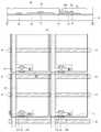
도 6a 내지 도 6d는 본 발명에 따른 전기영동표시장치의 드라이버층을 형성 하는 공정도이다. 여기서 도 6a 내지 도 6d는 평면도와 단면도를 같이 도시하며, 상기 단면도는 상기 평면도의 III-III'에 따른 단면도이다.6A through 6D are process diagrams for forming a driver layer of the electrophoretic display device according to the present invention. 6A to 6D show a plan view and a cross sectional view, wherein the cross section is a cross-sectional view taken along line III-III 'of the plan view.
도 6a에 도시된 바와 같이, 상기 기판(10)을 마련하고 상기 기판(10)상에 투명전도성 물질을 증착한다. 상기 투명전도성 물질을 패터닝하여 상기 화소셀(7) 영역에 상기 공통전극(20)을 형성한다. 여기서 상기 공통전극(20)은 큰 캐패시던스를 형성하기 위해 화소셀(7) 영역에 화면유지 충전전압을 유지하기 위해 소정의 면적을 차지하는 것이 바람직하다.As shown in FIG. 6A, the
상기 공통전극(20)은 투명전도성 물질로 형성되어 상기 전기영동 표시장치(1)의 드라이버층(5)을 투명하게 형성할 수 있게 된다. 즉, 전기영동 표시장치(1)는 양방향으로 이미지를 표시할 수 있게 된다.The
도 6b에 도시된 바와 같이, 상기 공통전극(20) 상에 게이트금속 물질을 증착하고 상기 게이트 금속물질에 패터닝을 실시하여 게이트라인(30) 및 공통라인(35)을 형성한다.As shown in FIG. 6B, a gate metal material is deposited on the
상기 게이트라인(30)은 돌기형상으로 돌출된 게이트전극(32)이 마련되어 추후에 상기 게이트전극(32)에 대응되는 영역에 스위칭소자(TR)가 형성된다.The
상기 공통라인(35)은 상기 공통전극(20) 상에 형성되어 서로 전기적으로 연결되도록 한다. 상기 공통라인(35)은 상기 게이트라인(30)에 평행한 방향으로 상기 공통전극(20) 상에 형성된다.The
그리고 상기 공통전극(20), 공통라인(35) 및 게이트라인(30)을 절연하는 게이트절연막(40)을 기판(10) 전면에 형성한다.A
한편, 상기 게이트전극(32)에서 돌출되어 있는 게이트전극(32) 상에는 게이트절연막(40) 상에 반도체층(50)을 형성하게 된다. 여기서 상기 반도체층(50)은 실리콘 등으로 형성할 수 있으며, 유기물질로 반도체층(50)을 형성함으로써 상기 전기영동표시장치(1)를 플렉서블하게 형성할 수도 있다.The
도 6c에 도시된 바와 같이, 상기 게이트절연막(40) 상에 데이터라인(60)을 형성한다. 상기 데이터라인(60)은 상기 게이트라인(30)에 교차하도록 형성된다. 상기 데이터라인(60)과 일체인 소스전극(60a)과 상기 소스전극(60a)에 소정간격 이격된 드레인전극(60b)은 상기 반도체층(50) 상에 형성된다. 이와 같이, 상기 데이터라인(60)과 상기 게이트라인(30)이 교차하는 영역에는 스위칭소자(Tr)가 형성된다.As shown in FIG. 6C, a
여기서 상기 데이터라인(60)이 형성된 기판(10) 상에 패시베이션막(70)을 형성한다. 상기 패시베이션막(70)은 스위칭소자(TR)를 보호하며, 상기 스위칭소자(TR)에 연결되는 다수의 라인(30, 60)을 보호하게 된다.The
그리고 상기 드레인전극(60b)에 대응되는 영역에 상기 패시베이션막(70)을 관통시켜 콘택홀(75)을 형성한다. 상기 콘택홀(75)은 상기 드레인전극(60b)의 일부를 노출시켜 추후에 형성되는 제1전극(80)과 상기 스위칭소자(TR)를 연결하게 된다.The
도 6d에 도시된 바와 같이, 상기 콘택홀(75)이 마련된 패시베이션막(70) 상에 제1전극(80)을 형성한다.As shown in FIG. 6D, the
상기 제1전극(80)은 ITO, IZO 등의 투명전도성 물질로 형성하는 것이 바람직하다. 그리고 상기 제1전극(80)은 게이트라인(30) 및 데이터라인(60) 상에도 형성 된다.The
여기서, 도 4를 참조하여 설명하면 전기영동 표시장치(1)는 다수의 대전입자(110)를 구비한 잉크층(3)에 의해서 영상을 표시할 수 있게 된다. 여기서 상기 잉크층(3)에 구비된 상기 대전입자(110)는 인가되는 전하에 따라 이동하게 되는데, 상기 게이트라인(30) 및 데이터라인(60)에 인가되는 전압에 의해서 상기 대전입자(110)도 반응하게 되어 스윙현상(Swing)이 발생할 수도 있다. 이에 따라 상기 대전입자(110)를 통제할 수 없는 상태가 될 수 있다.Here, referring to FIG. 4, the
따라서 상기 게이트라인(30), 데이터라인(60)에 인가되는 전압을 상기 대전입자(110)가 느끼지 못하도록 상기 데이터라인(60), 게이트라인(30) 상에 까지 상기 제1전극(80)을 형성하여 쉴딩(Sheiding)하는 것이 바람직하다.Accordingly, the
이와 같이, 전기영동 표시장치(1)의 드라이버층(5)에 투명전도성 물질로 상기 공통전극(20)을 형성함으로써 상기 공통전극(20)과 상기 제1전극(80) 간에 충분한 캐패시던스를 형성하여 전기영동 표시장치(1)의 화면유지 충전전압을 유지할 수 있게 된다. 또한 상기 투명전도성 물질로 형성된 공통전극(20)으로 인해 상기 전기영동 표시장치(1)의 후면에서도 화면을 이미지가 표시될 수 있게 된다. 즉, 상기 전기영동 표시장치(1)의 후면에서도 영상을 볼 수 있게 된다.In this manner, the
이로 인하여, 전기영동 표시장치(1)에 양면으로 디스플레이하기 위한 추가전력을 제공하지 않고도 양면으로 디스플레이할 수 있게 되고, 저소비전력으로 시야각 및 시인성이 우수한 표시장치를 제공할 수 있다.As a result, the
따라서 본 발명에 따른 전기영동 표시장치(1)는 하나의 표시장치로 양면으로 영상을 표시할 수 있게 된다. 이에 따라 공공장소 또는 다수의 사용자가 사용할 수 있는 공공 디스플레이(public display) 기능을 할 수 있게 된다.Therefore, the
상기한 바와 같이, 본 발명에 따른 전기영동 표시장치는 캐패시터로 사용하는 공통전극을 투명전도성 물질로 형성함으로써 양면으로 디스플레이하기 위한 추가전력을 제공하지 않고도 양면으로 디스플레이할 수 있게 되고, 편광된 빛으로 영상을 표시하지 않기 때문에 저소비전력으로 시야각 및 시인성이 우수한 표시장치를 제공할 수 있다.As described above, the electrophoretic display device according to the present invention forms a common electrode used as a capacitor with a transparent conductive material so that the display can be displayed on both sides without providing additional power for displaying on both sides, and the polarized light Since no image is displayed, a display device having excellent viewing angle and visibility with low power consumption can be provided.
또한 상기 전기영동 표시장치는 하나의 표시장치로 양면으로 영상을 표시할 수 있게 됨에 따라 공공장소 또는 다수의 사용자가 사용할 수 있는 공공 디스플레이(public display) 기능을 할 수 있는 효과가 있다.In addition, the electrophoretic display device can display an image on both sides with one display device, and thus has an effect of providing a public display function that can be used by a public place or by a plurality of users.
상기에서는 본 발명의 실시예를 참조하여 설명하였지만, 해당 기술 분야의 숙련된 당업자는 하기의 특허 청구 범위에 기재된 본 발명의 사상 및 영역으로부터 벗어나지 않는 범위 내에서 본 발명을 다양하게 수정 및 변경시킬 수 있음을 이해할 수 있을 것이다.It will be apparent to those skilled in the art that various modifications and variations can be made in the present invention without departing from the spirit or scope of the invention as defined in the appended claims. It can be understood that.
Claims (16)
Translated fromKoreanPriority Applications (1)
| Application Number | Priority Date | Filing Date | Title |
|---|---|---|---|
| KR1020060042795AKR101284921B1 (en) | 2006-05-12 | 2006-05-12 | electrophoretic display device and manufacturing method thereof |
Applications Claiming Priority (1)
| Application Number | Priority Date | Filing Date | Title |
|---|---|---|---|
| KR1020060042795AKR101284921B1 (en) | 2006-05-12 | 2006-05-12 | electrophoretic display device and manufacturing method thereof |
Publications (2)
| Publication Number | Publication Date |
|---|---|
| KR20070109603A KR20070109603A (en) | 2007-11-15 |
| KR101284921B1true KR101284921B1 (en) | 2013-07-10 |
Family
ID=39064092
Family Applications (1)
| Application Number | Title | Priority Date | Filing Date |
|---|---|---|---|
| KR1020060042795AExpired - Fee RelatedKR101284921B1 (en) | 2006-05-12 | 2006-05-12 | electrophoretic display device and manufacturing method thereof |
Country Status (1)
| Country | Link |
|---|---|
| KR (1) | KR101284921B1 (en) |
Families Citing this family (7)
| Publication number | Priority date | Publication date | Assignee | Title |
|---|---|---|---|---|
| US8902152B2 (en) | 2007-04-30 | 2014-12-02 | Motorola Mobility Llc | Dual sided electrophoretic display |
| US9122092B2 (en) | 2007-06-22 | 2015-09-01 | Google Technology Holdings LLC | Colored morphing apparatus for an electronic device |
| US8059232B2 (en) | 2008-02-08 | 2011-11-15 | Motorola Mobility, Inc. | Electronic device and LC shutter for polarization-sensitive switching between transparent and diffusive states |
| US7864270B2 (en) | 2008-02-08 | 2011-01-04 | Motorola, Inc. | Electronic device and LC shutter with diffusive reflective polarizer |
| KR101649226B1 (en)* | 2009-10-09 | 2016-08-19 | 엘지디스플레이 주식회사 | Display Device and Manufacturing Method of The Same |
| KR102024158B1 (en) | 2011-12-23 | 2019-09-24 | 삼성디스플레이 주식회사 | Display device |
| US11145262B2 (en)* | 2018-11-09 | 2021-10-12 | E Ink Corporation | Electro-optic displays |
Citations (2)
| Publication number | Priority date | Publication date | Assignee | Title |
|---|---|---|---|---|
| KR20020002089A (en)* | 2000-06-29 | 2002-01-09 | 주식회사 현대 디스플레이 테크놀로지 | Method of manufacturing lcd with high aperture ratio |
| KR20050045816A (en)* | 2003-11-12 | 2005-05-17 | 엘지.필립스 엘시디 주식회사 | Reflective type liquid crystal display device and method for fabricating the same |
- 2006
- 2006-05-12KRKR1020060042795Apatent/KR101284921B1/ennot_activeExpired - Fee Related
Patent Citations (2)
| Publication number | Priority date | Publication date | Assignee | Title |
|---|---|---|---|---|
| KR20020002089A (en)* | 2000-06-29 | 2002-01-09 | 주식회사 현대 디스플레이 테크놀로지 | Method of manufacturing lcd with high aperture ratio |
| KR20050045816A (en)* | 2003-11-12 | 2005-05-17 | 엘지.필립스 엘시디 주식회사 | Reflective type liquid crystal display device and method for fabricating the same |
Also Published As
| Publication number | Publication date |
|---|---|
| KR20070109603A (en) | 2007-11-15 |
Similar Documents
| Publication | Publication Date | Title |
|---|---|---|
| US7907126B2 (en) | Touch screen display device and method of manufacturing the same | |
| KR101880421B1 (en) | Electric field driving display device | |
| KR101659831B1 (en) | Liquid crystal display, method of driving the same, and method of manufacturing the same | |
| KR101284921B1 (en) | electrophoretic display device and manufacturing method thereof | |
| US7804639B2 (en) | Electrophoretic indication display | |
| US20130271445A1 (en) | Dual mode display device | |
| US20100039354A1 (en) | Display device and manufacturing method thereof | |
| TWI363919B (en) | Electrophoretic display device | |
| US20080158143A1 (en) | Electrophoretic display apparatus and method for manufacturing the same | |
| JP2008129599A (en) | Color filter substrate, electrophoretic display device including the same, and method for improving white light characteristics thereof | |
| US8564567B2 (en) | Electrophoretic display device using photo sensor | |
| CN109839779A (en) | Liquid crystal display panel | |
| KR20100069901A (en) | Electro phoretic display device including touch panel | |
| KR20110135131A (en) | Touch recognition liquid crystal display device | |
| US20080062506A1 (en) | Electronic paper apparatus | |
| US8068202B2 (en) | Liquid crystal device | |
| KR20100031241A (en) | Display substrate and display apparatus having the same | |
| KR101415569B1 (en) | Electrophoresis unit, display device having the same, and manufacturing method thereof | |
| KR20080099541A (en) | Display device and manufacturing method thereof | |
| JP5008030B2 (en) | Liquid crystal display | |
| TWI603140B (en) | Electrophoretic display | |
| KR20120016941A (en) | Electrophoresis display | |
| EP1909138A2 (en) | Electronic paper apparatus | |
| CN112703554B (en) | Display device and electronic equipment | |
| US10649293B2 (en) | Display device |
Legal Events
| Date | Code | Title | Description |
|---|---|---|---|
| PA0109 | Patent application | St.27 status event code:A-0-1-A10-A12-nap-PA0109 | |
| PG1501 | Laying open of application | St.27 status event code:A-1-1-Q10-Q12-nap-PG1501 | |
| PN2301 | Change of applicant | St.27 status event code:A-3-3-R10-R13-asn-PN2301 St.27 status event code:A-3-3-R10-R11-asn-PN2301 | |
| R18-X000 | Changes to party contact information recorded | St.27 status event code:A-3-3-R10-R18-oth-X000 | |
| A201 | Request for examination | ||
| PA0201 | Request for examination | St.27 status event code:A-1-2-D10-D11-exm-PA0201 | |
| R18-X000 | Changes to party contact information recorded | St.27 status event code:A-3-3-R10-R18-oth-X000 | |
| R18-X000 | Changes to party contact information recorded | St.27 status event code:A-3-3-R10-R18-oth-X000 | |
| PE0902 | Notice of grounds for rejection | St.27 status event code:A-1-2-D10-D21-exm-PE0902 | |
| E13-X000 | Pre-grant limitation requested | St.27 status event code:A-2-3-E10-E13-lim-X000 | |
| P11-X000 | Amendment of application requested | St.27 status event code:A-2-2-P10-P11-nap-X000 | |
| P13-X000 | Application amended | St.27 status event code:A-2-2-P10-P13-nap-X000 | |
| R17-X000 | Change to representative recorded | St.27 status event code:A-3-3-R10-R17-oth-X000 | |
| PE0902 | Notice of grounds for rejection | St.27 status event code:A-1-2-D10-D21-exm-PE0902 | |
| E13-X000 | Pre-grant limitation requested | St.27 status event code:A-2-3-E10-E13-lim-X000 | |
| P11-X000 | Amendment of application requested | St.27 status event code:A-2-2-P10-P11-nap-X000 | |
| P13-X000 | Application amended | St.27 status event code:A-2-2-P10-P13-nap-X000 | |
| E701 | Decision to grant or registration of patent right | ||
| PE0701 | Decision of registration | St.27 status event code:A-1-2-D10-D22-exm-PE0701 | |
| GRNT | Written decision to grant | ||
| PR0701 | Registration of establishment | St.27 status event code:A-2-4-F10-F11-exm-PR0701 | |
| PR1002 | Payment of registration fee | St.27 status event code:A-2-2-U10-U11-oth-PR1002 Fee payment year number:1 | |
| PG1601 | Publication of registration | St.27 status event code:A-4-4-Q10-Q13-nap-PG1601 | |
| FPAY | Annual fee payment | Payment date:20160630 Year of fee payment:4 | |
| PR1001 | Payment of annual fee | St.27 status event code:A-4-4-U10-U11-oth-PR1001 Fee payment year number:4 | |
| P22-X000 | Classification modified | St.27 status event code:A-4-4-P10-P22-nap-X000 | |
| PR1001 | Payment of annual fee | St.27 status event code:A-4-4-U10-U11-oth-PR1001 Fee payment year number:5 | |
| PR1001 | Payment of annual fee | St.27 status event code:A-4-4-U10-U11-oth-PR1001 Fee payment year number:6 | |
| FPAY | Annual fee payment | Payment date:20190617 Year of fee payment:7 | |
| PR1001 | Payment of annual fee | St.27 status event code:A-4-4-U10-U11-oth-PR1001 Fee payment year number:7 | |
| P22-X000 | Classification modified | St.27 status event code:A-4-4-P10-P22-nap-X000 | |
| PC1903 | Unpaid annual fee | St.27 status event code:A-4-4-U10-U13-oth-PC1903 Not in force date:20200705 Payment event data comment text:Termination Category : DEFAULT_OF_REGISTRATION_FEE | |
| PC1903 | Unpaid annual fee | St.27 status event code:N-4-6-H10-H13-oth-PC1903 Ip right cessation event data comment text:Termination Category : DEFAULT_OF_REGISTRATION_FEE Not in force date:20200705 |