KR101282383B1 - Liquid crystal display device and electronic device - Google Patents
Liquid crystal display device and electronic deviceDownload PDFInfo
- Publication number
- KR101282383B1 KR101282383B1KR1020137005820AKR20137005820AKR101282383B1KR 101282383 B1KR101282383 B1KR 101282383B1KR 1020137005820 AKR1020137005820 AKR 1020137005820AKR 20137005820 AKR20137005820 AKR 20137005820AKR 101282383 B1KR101282383 B1KR 101282383B1
- Authority
- KR
- South Korea
- Prior art keywords
- liquid crystal
- transistor
- oxide semiconductor
- crystal display
- layer
- Prior art date
- Legal status (The legal status is an assumption and is not a legal conclusion. Google has not performed a legal analysis and makes no representation as to the accuracy of the status listed.)
- Active
Links
Images


Classifications
- H—ELECTRICITY
- H10—SEMICONDUCTOR DEVICES; ELECTRIC SOLID-STATE DEVICES NOT OTHERWISE PROVIDED FOR
- H10D—INORGANIC ELECTRIC SEMICONDUCTOR DEVICES
- H10D30/00—Field-effect transistors [FET]
- H10D30/60—Insulated-gate field-effect transistors [IGFET]
- H10D30/67—Thin-film transistors [TFT]
- H10D30/674—Thin-film transistors [TFT] characterised by the active materials
- H10D30/6755—Oxide semiconductors, e.g. zinc oxide, copper aluminium oxide or cadmium stannate
- G—PHYSICS
- G02—OPTICS
- G02F—OPTICAL DEVICES OR ARRANGEMENTS FOR THE CONTROL OF LIGHT BY MODIFICATION OF THE OPTICAL PROPERTIES OF THE MEDIA OF THE ELEMENTS INVOLVED THEREIN; NON-LINEAR OPTICS; FREQUENCY-CHANGING OF LIGHT; OPTICAL LOGIC ELEMENTS; OPTICAL ANALOGUE/DIGITAL CONVERTERS
- G02F1/00—Devices or arrangements for the control of the intensity, colour, phase, polarisation or direction of light arriving from an independent light source, e.g. switching, gating or modulating; Non-linear optics
- G02F1/01—Devices or arrangements for the control of the intensity, colour, phase, polarisation or direction of light arriving from an independent light source, e.g. switching, gating or modulating; Non-linear optics for the control of the intensity, phase, polarisation or colour
- G02F1/13—Devices or arrangements for the control of the intensity, colour, phase, polarisation or direction of light arriving from an independent light source, e.g. switching, gating or modulating; Non-linear optics for the control of the intensity, phase, polarisation or colour based on liquid crystals, e.g. single liquid crystal display cells
- G02F1/133—Constructional arrangements; Operation of liquid crystal cells; Circuit arrangements
- G02F1/1333—Constructional arrangements; Manufacturing methods
- G02F1/13338—Input devices, e.g. touch panels
- G—PHYSICS
- G02—OPTICS
- G02F—OPTICAL DEVICES OR ARRANGEMENTS FOR THE CONTROL OF LIGHT BY MODIFICATION OF THE OPTICAL PROPERTIES OF THE MEDIA OF THE ELEMENTS INVOLVED THEREIN; NON-LINEAR OPTICS; FREQUENCY-CHANGING OF LIGHT; OPTICAL LOGIC ELEMENTS; OPTICAL ANALOGUE/DIGITAL CONVERTERS
- G02F1/00—Devices or arrangements for the control of the intensity, colour, phase, polarisation or direction of light arriving from an independent light source, e.g. switching, gating or modulating; Non-linear optics
- G02F1/01—Devices or arrangements for the control of the intensity, colour, phase, polarisation or direction of light arriving from an independent light source, e.g. switching, gating or modulating; Non-linear optics for the control of the intensity, phase, polarisation or colour
- G02F1/13—Devices or arrangements for the control of the intensity, colour, phase, polarisation or direction of light arriving from an independent light source, e.g. switching, gating or modulating; Non-linear optics for the control of the intensity, phase, polarisation or colour based on liquid crystals, e.g. single liquid crystal display cells
- G02F1/133—Constructional arrangements; Operation of liquid crystal cells; Circuit arrangements
- G02F1/136—Liquid crystal cells structurally associated with a semi-conducting layer or substrate, e.g. cells forming part of an integrated circuit
- G02F1/1362—Active matrix addressed cells
- G02F1/136286—Wiring, e.g. gate line, drain line
- G—PHYSICS
- G02—OPTICS
- G02F—OPTICAL DEVICES OR ARRANGEMENTS FOR THE CONTROL OF LIGHT BY MODIFICATION OF THE OPTICAL PROPERTIES OF THE MEDIA OF THE ELEMENTS INVOLVED THEREIN; NON-LINEAR OPTICS; FREQUENCY-CHANGING OF LIGHT; OPTICAL LOGIC ELEMENTS; OPTICAL ANALOGUE/DIGITAL CONVERTERS
- G02F1/00—Devices or arrangements for the control of the intensity, colour, phase, polarisation or direction of light arriving from an independent light source, e.g. switching, gating or modulating; Non-linear optics
- G02F1/01—Devices or arrangements for the control of the intensity, colour, phase, polarisation or direction of light arriving from an independent light source, e.g. switching, gating or modulating; Non-linear optics for the control of the intensity, phase, polarisation or colour
- G02F1/13—Devices or arrangements for the control of the intensity, colour, phase, polarisation or direction of light arriving from an independent light source, e.g. switching, gating or modulating; Non-linear optics for the control of the intensity, phase, polarisation or colour based on liquid crystals, e.g. single liquid crystal display cells
- G02F1/133—Constructional arrangements; Operation of liquid crystal cells; Circuit arrangements
- G02F1/136—Liquid crystal cells structurally associated with a semi-conducting layer or substrate, e.g. cells forming part of an integrated circuit
- G02F1/1362—Active matrix addressed cells
- G02F1/1368—Active matrix addressed cells in which the switching element is a three-electrode device
- G—PHYSICS
- G09—EDUCATION; CRYPTOGRAPHY; DISPLAY; ADVERTISING; SEALS
- G09G—ARRANGEMENTS OR CIRCUITS FOR CONTROL OF INDICATING DEVICES USING STATIC MEANS TO PRESENT VARIABLE INFORMATION
- G09G3/00—Control arrangements or circuits, of interest only in connection with visual indicators other than cathode-ray tubes
- G09G3/20—Control arrangements or circuits, of interest only in connection with visual indicators other than cathode-ray tubes for presentation of an assembly of a number of characters, e.g. a page, by composing the assembly by combination of individual elements arranged in a matrix no fixed position being assigned to or needed to be assigned to the individual characters or partial characters
- G09G3/34—Control arrangements or circuits, of interest only in connection with visual indicators other than cathode-ray tubes for presentation of an assembly of a number of characters, e.g. a page, by composing the assembly by combination of individual elements arranged in a matrix no fixed position being assigned to or needed to be assigned to the individual characters or partial characters by control of light from an independent source
- G09G3/36—Control arrangements or circuits, of interest only in connection with visual indicators other than cathode-ray tubes for presentation of an assembly of a number of characters, e.g. a page, by composing the assembly by combination of individual elements arranged in a matrix no fixed position being assigned to or needed to be assigned to the individual characters or partial characters by control of light from an independent source using liquid crystals
- G09G3/3611—Control of matrices with row and column drivers
- G09G3/3674—Details of drivers for scan electrodes
- G09G3/3677—Details of drivers for scan electrodes suitable for active matrices only
- H—ELECTRICITY
- H01—ELECTRIC ELEMENTS
- H01L—SEMICONDUCTOR DEVICES NOT COVERED BY CLASS H10
- H01L21/00—Processes or apparatus adapted for the manufacture or treatment of semiconductor or solid state devices or of parts thereof
- H01L21/02—Manufacture or treatment of semiconductor devices or of parts thereof
- H01L21/02104—Forming layers
- H01L21/02365—Forming inorganic semiconducting materials on a substrate
- H01L21/02436—Intermediate layers between substrates and deposited layers
- H01L21/02439—Materials
- H01L21/02483—Oxide semiconducting materials not being Group 12/16 materials, e.g. ternary compounds
- H—ELECTRICITY
- H10—SEMICONDUCTOR DEVICES; ELECTRIC SOLID-STATE DEVICES NOT OTHERWISE PROVIDED FOR
- H10D—INORGANIC ELECTRIC SEMICONDUCTOR DEVICES
- H10D30/00—Field-effect transistors [FET]
- H10D30/60—Insulated-gate field-effect transistors [IGFET]
- H10D30/67—Thin-film transistors [TFT]
- H10D30/6704—Thin-film transistors [TFT] having supplementary regions or layers in the thin films or in the insulated bulk substrates for controlling properties of the device
- H10D30/6706—Thin-film transistors [TFT] having supplementary regions or layers in the thin films or in the insulated bulk substrates for controlling properties of the device for preventing leakage current
- H—ELECTRICITY
- H10—SEMICONDUCTOR DEVICES; ELECTRIC SOLID-STATE DEVICES NOT OTHERWISE PROVIDED FOR
- H10D—INORGANIC ELECTRIC SEMICONDUCTOR DEVICES
- H10D86/00—Integrated devices formed in or on insulating or conducting substrates, e.g. formed in silicon-on-insulator [SOI] substrates or on stainless steel or glass substrates
- H10D86/40—Integrated devices formed in or on insulating or conducting substrates, e.g. formed in silicon-on-insulator [SOI] substrates or on stainless steel or glass substrates characterised by multiple TFTs
- H10D86/421—Integrated devices formed in or on insulating or conducting substrates, e.g. formed in silicon-on-insulator [SOI] substrates or on stainless steel or glass substrates characterised by multiple TFTs having a particular composition, shape or crystalline structure of the active layer
- H10D86/423—Integrated devices formed in or on insulating or conducting substrates, e.g. formed in silicon-on-insulator [SOI] substrates or on stainless steel or glass substrates characterised by multiple TFTs having a particular composition, shape or crystalline structure of the active layer comprising semiconductor materials not belonging to the Group IV, e.g. InGaZnO
- H—ELECTRICITY
- H10—SEMICONDUCTOR DEVICES; ELECTRIC SOLID-STATE DEVICES NOT OTHERWISE PROVIDED FOR
- H10D—INORGANIC ELECTRIC SEMICONDUCTOR DEVICES
- H10D86/00—Integrated devices formed in or on insulating or conducting substrates, e.g. formed in silicon-on-insulator [SOI] substrates or on stainless steel or glass substrates
- H10D86/40—Integrated devices formed in or on insulating or conducting substrates, e.g. formed in silicon-on-insulator [SOI] substrates or on stainless steel or glass substrates characterised by multiple TFTs
- H10D86/481—Integrated devices formed in or on insulating or conducting substrates, e.g. formed in silicon-on-insulator [SOI] substrates or on stainless steel or glass substrates characterised by multiple TFTs integrated with passive devices, e.g. auxiliary capacitors
- H—ELECTRICITY
- H10—SEMICONDUCTOR DEVICES; ELECTRIC SOLID-STATE DEVICES NOT OTHERWISE PROVIDED FOR
- H10D—INORGANIC ELECTRIC SEMICONDUCTOR DEVICES
- H10D86/00—Integrated devices formed in or on insulating or conducting substrates, e.g. formed in silicon-on-insulator [SOI] substrates or on stainless steel or glass substrates
- H10D86/40—Integrated devices formed in or on insulating or conducting substrates, e.g. formed in silicon-on-insulator [SOI] substrates or on stainless steel or glass substrates characterised by multiple TFTs
- H10D86/60—Integrated devices formed in or on insulating or conducting substrates, e.g. formed in silicon-on-insulator [SOI] substrates or on stainless steel or glass substrates characterised by multiple TFTs wherein the TFTs are in active matrices
- G—PHYSICS
- G06—COMPUTING OR CALCULATING; COUNTING
- G06F—ELECTRIC DIGITAL DATA PROCESSING
- G06F3/00—Input arrangements for transferring data to be processed into a form capable of being handled by the computer; Output arrangements for transferring data from processing unit to output unit, e.g. interface arrangements
- G06F3/01—Input arrangements or combined input and output arrangements for interaction between user and computer
- G06F3/03—Arrangements for converting the position or the displacement of a member into a coded form
- G06F3/041—Digitisers, e.g. for touch screens or touch pads, characterised by the transducing means
- G06F3/0412—Digitisers structurally integrated in a display
- G—PHYSICS
- G06—COMPUTING OR CALCULATING; COUNTING
- G06F—ELECTRIC DIGITAL DATA PROCESSING
- G06F3/00—Input arrangements for transferring data to be processed into a form capable of being handled by the computer; Output arrangements for transferring data from processing unit to output unit, e.g. interface arrangements
- G06F3/01—Input arrangements or combined input and output arrangements for interaction between user and computer
- G06F3/03—Arrangements for converting the position or the displacement of a member into a coded form
- G06F3/041—Digitisers, e.g. for touch screens or touch pads, characterised by the transducing means
- G06F3/044—Digitisers, e.g. for touch screens or touch pads, characterised by the transducing means by capacitive means
- G—PHYSICS
- G06—COMPUTING OR CALCULATING; COUNTING
- G06F—ELECTRIC DIGITAL DATA PROCESSING
- G06F3/00—Input arrangements for transferring data to be processed into a form capable of being handled by the computer; Output arrangements for transferring data from processing unit to output unit, e.g. interface arrangements
- G06F3/01—Input arrangements or combined input and output arrangements for interaction between user and computer
- G06F3/03—Arrangements for converting the position or the displacement of a member into a coded form
- G06F3/041—Digitisers, e.g. for touch screens or touch pads, characterised by the transducing means
- G06F3/045—Digitisers, e.g. for touch screens or touch pads, characterised by the transducing means using resistive elements, e.g. a single continuous surface or two parallel surfaces put in contact
- G—PHYSICS
- G09—EDUCATION; CRYPTOGRAPHY; DISPLAY; ADVERTISING; SEALS
- G09G—ARRANGEMENTS OR CIRCUITS FOR CONTROL OF INDICATING DEVICES USING STATIC MEANS TO PRESENT VARIABLE INFORMATION
- G09G2300/00—Aspects of the constitution of display devices
- G09G2300/04—Structural and physical details of display devices
- G09G2300/0421—Structural details of the set of electrodes
- G09G2300/0426—Layout of electrodes and connections
- G—PHYSICS
- G09—EDUCATION; CRYPTOGRAPHY; DISPLAY; ADVERTISING; SEALS
- G09G—ARRANGEMENTS OR CIRCUITS FOR CONTROL OF INDICATING DEVICES USING STATIC MEANS TO PRESENT VARIABLE INFORMATION
- G09G2310/00—Command of the display device
- G09G2310/04—Partial updating of the display screen
- G—PHYSICS
- G09—EDUCATION; CRYPTOGRAPHY; DISPLAY; ADVERTISING; SEALS
- G09G—ARRANGEMENTS OR CIRCUITS FOR CONTROL OF INDICATING DEVICES USING STATIC MEANS TO PRESENT VARIABLE INFORMATION
- G09G2310/00—Command of the display device
- G09G2310/08—Details of timing specific for flat panels, other than clock recovery
- G—PHYSICS
- G09—EDUCATION; CRYPTOGRAPHY; DISPLAY; ADVERTISING; SEALS
- G09G—ARRANGEMENTS OR CIRCUITS FOR CONTROL OF INDICATING DEVICES USING STATIC MEANS TO PRESENT VARIABLE INFORMATION
- G09G2320/00—Control of display operating conditions
- G09G2320/02—Improving the quality of display appearance
- G09G2320/0209—Crosstalk reduction, i.e. to reduce direct or indirect influences of signals directed to a certain pixel of the displayed image on other pixels of said image, inclusive of influences affecting pixels in different frames or fields or sub-images which constitute a same image, e.g. left and right images of a stereoscopic display
- G09G2320/0214—Crosstalk reduction, i.e. to reduce direct or indirect influences of signals directed to a certain pixel of the displayed image on other pixels of said image, inclusive of influences affecting pixels in different frames or fields or sub-images which constitute a same image, e.g. left and right images of a stereoscopic display with crosstalk due to leakage current of pixel switch in active matrix panels
- G—PHYSICS
- G09—EDUCATION; CRYPTOGRAPHY; DISPLAY; ADVERTISING; SEALS
- G09G—ARRANGEMENTS OR CIRCUITS FOR CONTROL OF INDICATING DEVICES USING STATIC MEANS TO PRESENT VARIABLE INFORMATION
- G09G2320/00—Control of display operating conditions
- G09G2320/02—Improving the quality of display appearance
- G09G2320/0247—Flicker reduction other than flicker reduction circuits used for single beam cathode-ray tubes
- G—PHYSICS
- G09—EDUCATION; CRYPTOGRAPHY; DISPLAY; ADVERTISING; SEALS
- G09G—ARRANGEMENTS OR CIRCUITS FOR CONTROL OF INDICATING DEVICES USING STATIC MEANS TO PRESENT VARIABLE INFORMATION
- G09G2320/00—Control of display operating conditions
- G09G2320/04—Maintaining the quality of display appearance
- G09G2320/043—Preventing or counteracting the effects of ageing
- G—PHYSICS
- G09—EDUCATION; CRYPTOGRAPHY; DISPLAY; ADVERTISING; SEALS
- G09G—ARRANGEMENTS OR CIRCUITS FOR CONTROL OF INDICATING DEVICES USING STATIC MEANS TO PRESENT VARIABLE INFORMATION
- G09G2320/00—Control of display operating conditions
- G09G2320/10—Special adaptations of display systems for operation with variable images
- G09G2320/103—Detection of image changes, e.g. determination of an index representative of the image change
- G—PHYSICS
- G09—EDUCATION; CRYPTOGRAPHY; DISPLAY; ADVERTISING; SEALS
- G09G—ARRANGEMENTS OR CIRCUITS FOR CONTROL OF INDICATING DEVICES USING STATIC MEANS TO PRESENT VARIABLE INFORMATION
- G09G2330/00—Aspects of power supply; Aspects of display protection and defect management
- G09G2330/02—Details of power systems and of start or stop of display operation
- G09G2330/021—Power management, e.g. power saving
- G—PHYSICS
- G09—EDUCATION; CRYPTOGRAPHY; DISPLAY; ADVERTISING; SEALS
- G09G—ARRANGEMENTS OR CIRCUITS FOR CONTROL OF INDICATING DEVICES USING STATIC MEANS TO PRESENT VARIABLE INFORMATION
- G09G3/00—Control arrangements or circuits, of interest only in connection with visual indicators other than cathode-ray tubes
- G09G3/20—Control arrangements or circuits, of interest only in connection with visual indicators other than cathode-ray tubes for presentation of an assembly of a number of characters, e.g. a page, by composing the assembly by combination of individual elements arranged in a matrix no fixed position being assigned to or needed to be assigned to the individual characters or partial characters
- G09G3/34—Control arrangements or circuits, of interest only in connection with visual indicators other than cathode-ray tubes for presentation of an assembly of a number of characters, e.g. a page, by composing the assembly by combination of individual elements arranged in a matrix no fixed position being assigned to or needed to be assigned to the individual characters or partial characters by control of light from an independent source
- G09G3/36—Control arrangements or circuits, of interest only in connection with visual indicators other than cathode-ray tubes for presentation of an assembly of a number of characters, e.g. a page, by composing the assembly by combination of individual elements arranged in a matrix no fixed position being assigned to or needed to be assigned to the individual characters or partial characters by control of light from an independent source using liquid crystals
- G09G3/3611—Control of matrices with row and column drivers
- G09G3/3648—Control of matrices with row and column drivers using an active matrix
Landscapes
- Physics & Mathematics (AREA)
- Engineering & Computer Science (AREA)
- Nonlinear Science (AREA)
- General Physics & Mathematics (AREA)
- Chemical & Material Sciences (AREA)
- Crystallography & Structural Chemistry (AREA)
- Optics & Photonics (AREA)
- Mathematical Physics (AREA)
- Microelectronics & Electronic Packaging (AREA)
- Computer Hardware Design (AREA)
- Theoretical Computer Science (AREA)
- Power Engineering (AREA)
- Manufacturing & Machinery (AREA)
- Condensed Matter Physics & Semiconductors (AREA)
- Thin Film Transistor (AREA)
- Liquid Crystal (AREA)
- Control Of Indicators Other Than Cathode Ray Tubes (AREA)
- Liquid Crystal Display Device Control (AREA)
- Devices For Indicating Variable Information By Combining Individual Elements (AREA)
Abstract
Translated fromKoreanDescription
Translated fromKorean본 발명은, 액정 표시 장치 및 이 액정 표시 장치를 갖는 전자 기기에 관한 것이다.The present invention relates to a liquid crystal display device and an electronic apparatus having the liquid crystal display device.
액정 표시 장치는, 텔레비전 수상기 등의 대형 표시 장치에서 휴대 전화 등의 소형 표시 장치에 이르기까지 보급되어 있다. 이로 인해, 액정 표시 장치의 개발은, 저비용화 또는 고부가가치화를 목적으로 한 개발이 이루어지고 있다. 특히 근래에는, 지구 환경에의 관심이 높아지고, 저소비 전력형의 액정 표시 장치의 개발이 주목받고 있다.
Liquid crystal displays are spreading from large display devices such as television receivers to small display devices such as mobile phones. For this reason, the development of the liquid crystal display device for the purpose of cost reduction or high added value is made | formed. In particular, in recent years, interest in the global environment has increased, and development of a low power consumption liquid crystal display device has attracted attention.
*특허문헌 1에서는, 액정 표시 장치에서의 소비 전력을 저감하는 기술이 개시되어 있다. 구체적으로는, 모든 주사선 및 데이터 신호선을 비선택 상태로 하는 휴지 기간에, 모든 데이터 신호선을 전기적으로 데이터 신호 드라이버에서 절리하여 하이 임피던스 상태로 하는 액정 표시 장치가 개시되어 있다.* Patent Literature 1 discloses a technique for reducing power consumption in a liquid crystal display device. More specifically, a liquid crystal display device is disclosed in which all data signal lines are electrically cut by a data signal driver to be in a high impedance state in an idle period in which all of the scan lines and the data signal lines are in an unselected state.
일반적으로, 액정 표시 장치는, 매트릭스형으로 배열된 복수의 화소가 형성된 화소부를 갖는다. 이 화소는, 화상 신호의 입력을 제어하는 트랜지스터와, 입력되는 화상 신호에 따른 전압이 인가되는 액정 소자와, 이 액정 소자에 인가되는 전압을 유지하는 보조 용량을 갖는다. 한편, 이 액정 소자는 인가되는 전압에 따라 배향이 변화하는 액정 재료를 갖고, 이 액정 재료의 배향을 제어함으로써 각 화소의 표시가 제어된다.Generally, a liquid crystal display device has the pixel part in which the some pixel arranged in the matrix form was formed. This pixel has a transistor for controlling the input of an image signal, a liquid crystal element to which a voltage corresponding to the input image signal is applied, and a storage capacitor holding a voltage applied to the liquid crystal element. On the other hand, this liquid crystal element has a liquid crystal material whose orientation changes depending on the voltage applied, and the display of each pixel is controlled by controlling the orientation of this liquid crystal material.
특허문헌 1에 개시된 액정 표시 장치에서는, 휴지 기간에서, 화소부에 포함되는 각 화소에 대해 화상 신호가 입력되지 않는다. 즉, 각 화소 내에 화상 신호를 유지한 채로, 화상 신호의 입력을 제어하는 트랜지스터가 오프 상태를 유지하는 기간이 장기화된다. 이로 인해, 이 트랜지스터를 통한 화상 신호의 리크가 각 화소의 표시에 대해 주는 영향이 현재화한다. 구체적으로는, 액정 소자에 인가되는 전압이 저하되고, 이 액정 소자를 갖는 화소의 표시의 열화(변화)가 현재화한다.In the liquid crystal display device disclosed in Patent Literature 1, an image signal is not input to each pixel included in the pixel portion during the rest period. That is, the period during which the transistor controlling the input of the image signal is kept off while the image signal is held in each pixel is extended. For this reason, the influence that the leak of the image signal through this transistor has on the display of each pixel is made manifest. Specifically, the voltage applied to the liquid crystal element is lowered and the deterioration (change) of the display of the pixel having this liquid crystal element is present.
나아가, 이 트랜지스터를 통한 화상 신호의 리크는, 트랜지스터의 동작 온도에 의해 변동한다. 구체적으로는, 동작 온도의 상승에 따라, 트랜지스터를 통한 화상 신호의 리크가 증가한다. 이로 인해, 특허문헌 1에 개시된 액정 표시 장치는, 환경의 변동이 큰 옥외 등에서 사용하였을 때, 표시 품질을 일정하게 유지하기 어렵다.Further, the leakage of the image signal through this transistor varies with the operating temperature of the transistor. Specifically, as the operating temperature rises, the leak of the image signal through the transistor increases. For this reason, when using the liquid crystal display device disclosed by patent document 1 in the outdoors etc. with large fluctuation | variation of an environment, it is difficult to keep display quality constant.
따라서, 본 발명의 일 양태는, 액정 표시 장치의 소비 전력을 저감하는 것 및 표시의 열화(표시 품질의 저하)를 억제하는 것을 과제의 하나로 한다.Therefore, one aspect of this invention makes it one of a subject to reduce the power consumption of a liquid crystal display device, and to suppress display deterioration (degradation of display quality).
또한, 본 발명의 일 양태는, 온도 등의 외부 인자에 대한 표시의 열화(표시 품질의 저하)가 억제된 액정 표시 장치를 제공하는 것을 과제의 하나로 한다.Another object of the present invention is to provide a liquid crystal display device in which deterioration of display (decrease in display quality) to external factors such as temperature is suppressed.
상기한 과제는, 각 화소에 형성되는 트랜지스터로, 채널 형성 영역이 산화물 반도체층에 의해 구성되는 트랜지스터를 적용함으로써 해결할 수 있다. 한편, 이 산화물 반도체층은, 전자 공여체(도너)가 되는 불순물(수소 또는 물 등)을 철저히 제거함으로써 고순도화된 산화물 반도체층이다. 이 트랜지스터로는, 채널 길이 10㎛인 경우에, 실온에서의 채널 폭 1㎛ 당 오프 전류값을 10aA(1×10-17A) 이하로 하는 것이 가능하다(이를 10aA/㎛로 나타낸다).The above-described problems can be solved by applying a transistor formed in each pixel in which a channel formation region is formed of an oxide semiconductor layer. On the other hand, this oxide semiconductor layer is an oxide semiconductor layer which has been highly purified by thoroughly removing impurities (such as hydrogen or water) which becomes an electron donor (donor). In this transistor, when the channel length is 10 m, it is possible to set the off current value per 1 m of the channel width at room temperature to 10 aA (1 x 10-17 A) or less (this is represented by 10 aA / m).
또한, 이 산화물 반도체층은, 2.0eV 이상, 바람직하게는 2.5eV 이상, 더욱 바람직하게는 3.0eV 이상의 밴드갭을 갖는다. 나아가, 이 산화물 반도체층은, 고순도화됨으로써, 도전형이 무한대로 진성형에 가까워진다. 이로 인해, 이 산화물 반도체층에서는, 열여기에 기인하는 캐리어의 발생을 억제할 수 있다. 그 결과, 이 트랜지스터의 동작 온도의 상승에 따른 오프 전류의 증가를 저감할 수 있다. 구체적으로는, 채널 길이 10㎛인 경우에, 85℃에서의 채널 폭 1㎛ 당 오프 전류값을 100aA(1×10-16A) 이하로 하는 것이 가능하다(이를 100aA/㎛라 표기한다).Further, the oxide semiconductor layer has a bandgap of 2.0 eV or more, preferably 2.5 eV or more, more preferably 3.0 eV or more. Furthermore, this oxide semiconductor layer is made highly purified, whereby the conductivity type approaches intrinsic form indefinitely. For this reason, in this oxide semiconductor layer, generation | occurrence | production of the carrier resulting from heat excitation can be suppressed. As a result, an increase in the off current due to the increase in the operating temperature of the transistor can be reduced. Specifically, in the case of a channel length of 10 µm, it is possible to set the off current value per channel width of 1 µm at 85 ° C to 100 aA (1 × 10-16 A) or less (this is referred to as 100 aA / µm).
구체적으로는, 본 발명의 일 양태는, 주사선 구동 회로에 의해 스위칭이 제어되는 트랜지스터와, 한쪽 단자에 신호선 구동 회로에서 상기 트랜지스터를 통하여 화상 신호가 입력되고, 다른 한쪽 단자에 공통 전위가 공급됨으로써, 상기 화상 신호에 따른 전압이 인가되는 액정 소자와, 상기 액정 소자에 인가되는 전압을 유지하는 용량 소자와, 를 갖는 복수의 화소가 매트릭스형으로 배열된 액정 표시 장치로써, 상기 주사선 구동 회로 및 상기 신호선 구동 회로의 동작을 제어하고, 상기 화소로의 상기 화상 신호의 입력을 선택하는 제어 회로를 갖고, 상기 트랜지스터는, 채널 형성 영역이 산화물 반도체층에 의해 구성되고, 오프 상태의 상기 트랜지스터를 통한 상기 화상 신호의 리크가, 상기 액정 소자를 통한 상기 화상 신호의 리크 보다도 작은 것을 특징으로 하는 액정 표시 장치이다.Specifically, in one aspect of the present invention, an image signal is inputted through a transistor whose switching is controlled by a scanning line driver circuit, and a signal line driver circuit is input to one terminal, and a common potential is supplied to the other terminal. A liquid crystal display in which a liquid crystal element to which a voltage according to the image signal is applied, a capacitive element to hold a voltage applied to the liquid crystal element, and a plurality of pixels having are arranged in a matrix, wherein the scan line driver circuit and the signal line A control circuit which controls the operation of the driving circuit and selects the input of the image signal to the pixel, wherein the transistor has a channel formation region formed by an oxide semiconductor layer, and the image through the transistor in an off state. The leak of the signal is smaller than the leak of the image signal through the liquid crystal element. A liquid crystal display device as ranging.
본 발명의 일 양태의 액정 표시 장치는, 각 화소에 형성되는 트랜지스터로, 채널 형성 영역이 산화물 반도체층에 의해 구성되는 트랜지스터를 적용한다. 한편, 이 산화물 반도체층을 고순도화함으로써, 이 트랜지스터의 실온에서의 오프 전류값을 10aA/㎛ 이하, 또한 85℃에서의 오프 전류값을 100aA/㎛ 이하로 하는 것이 가능하다. 이로 인해, 이 트랜지스터를 통한 화상 신호의 리크를 저감할 수 있다. 즉, 이 트랜지스터를 갖는 화소로의 화상 신호의 쓰기 빈도를 저감한 경우에서의 표시의 열화(변화)를 억제할 수 있다. 그 결과, 이 액정 표시 장치의 소비 전력을 저감하는 것 및 표시의 열화(표시 품질의 저하)를 억제할 수 있게 된다.In the liquid crystal display device of one embodiment of the present invention, a transistor formed in each pixel applies a transistor in which a channel formation region is formed of an oxide semiconductor layer. On the other hand, by making this oxide semiconductor layer highly purified, it is possible to make the off current value at room temperature of this transistor 10aA / micrometer or less, and the off current value at 85 degreeC to 100aA / micrometer or less. For this reason, the leak of the image signal through this transistor can be reduced. That is, deterioration (change) of the display can be suppressed when the frequency of writing the image signal to the pixel having this transistor is reduced. As a result, it is possible to reduce the power consumption of the liquid crystal display device and to suppress deterioration of the display (degradation of display quality).
또한, 상기한 바와 같이, 이 트랜지스터는, 85℃라는 고온에서도 오프 전류값을 100aA/㎛ 이하로 하는 것이 가능하다. 즉, 이 트랜지스터는, 동작 온도의 상승에 따른 오프 전류값의 증가가 현저하게 작은 트랜지스터이다. 이로 인해, 이 트랜지스터를 액정 표시 장치의 각 화소에 형성되는 트랜지스터로 적용함으로써, 온도 등의 외부 인자가 이 화소에서의 화상 신호의 리크에 가하는 영향을 저감할 수 있다. 즉, 이 액정 표시 장치는, 환경의 변동이 큰 옥외 등에서 사용한 경우라도, 표시의 열화(표시 품질의 저하)를 억제하는 것이 가능한 액정 표시 장치이다.As described above, the transistor can set the off current value to 100aA / µm or less even at a high temperature of 85 ° C. That is, this transistor is a transistor in which the increase in the off current value with the increase of the operating temperature is remarkably small. For this reason, by applying this transistor to the transistor formed in each pixel of a liquid crystal display device, the influence which an external factor, such as temperature, exerts on the leak of the image signal in this pixel can be reduced. That is, this liquid crystal display device is a liquid crystal display device which can suppress deterioration (deterioration of display quality) of a display even when used in the outdoor etc. with large fluctuation | variation of an environment.
도 1(A), (B)는, 실시형태 1에 관한 액정 표시 장치를 설명하는 도면이다.
도 2는, 실시형태 1에 관한 액정 표시 장치를 설명하는 도면이다.
도 3(A)~(C)는, 실시형태 1에 관한 액정 표시 장치를 설명하는 도면이다.
도 4(A)~(D)는, 실시형태 2에 관한 트랜지스터를 설명하는 도면이다.
도 5(A), (B)는, 실시형태 3에 관한 액정 표시 장치를 설명하는 도면이다.
도 6(A)~(F)는, 실시형태 4에 관한 전자 기기를 설명하는 도면이다.
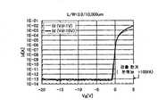
도 7은, 실시예 1에 관한 트랜지스터의 초기 특성을 나타낸 도면이다.
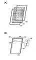
도 8(A), (B)는, 실시예 1에 관한 트랜지스터의 평가용 소자의 상면도이다.
도 9(A), (B)는, 실시예 1에 관한 트랜지스터의 평가용 소자의 Vg-Id 특성을 나타낸 도면이다.FIG.1 (A), (B) is a figure explaining the liquid crystal display device which concerns on Embodiment 1. FIG.
FIG. 2 is a diagram illustrating a liquid crystal display device according to the first embodiment.
FIG.3 (A)-(C) is a figure explaining the liquid crystal display device which concerns on Embodiment 1. FIG.
4A to 4D are diagrams illustrating the transistor according to the second embodiment.
FIG. 5: (A), (B) is a figure explaining the liquid crystal display device which concerns on Embodiment 3. FIG.
6 (A) to (F) are diagrams for explaining the electronic apparatus according to the fourth embodiment.
7 is a diagram showing initial characteristics of the transistor according to the first embodiment.
8A and 8B are top views of elements for evaluating the transistor according to the first embodiment.
9A and 9B show the Vg-Id characteristics of the evaluation device for the transistor according to Example 1. FIG.
이하에서는, 본 발명의 실시형태에 대해 도면을 이용하여 상세히 설명한다. 단, 본 발명은 이하의 설명에 한정되지 않고, 본 발명의 취지 및 그 범위에서 벗어나지 않는 한도 내에서 그 형태 및 상세한 내용을 다양하게 변경할 수 있다는 것은, 당업자라면 용이하게 이해할 수 있다. 따라서, 본 발명은 이하에 나타낸 실시형태의 기재 내용에 한정되어 해석되어서는 안 된다.EMBODIMENT OF THE INVENTION Hereinafter, embodiment of this invention is described in detail using drawing. However, the present invention is not limited to the following description, and it can be easily understood by those skilled in the art that various changes can be made in form and detail of the present invention without departing from the spirit and scope of the present invention. Therefore, this invention should not be interpreted limited to the description of embodiment shown below.
한편, 트랜지스터의 소스 단자 및 드레인 단자는, 트랜지스터의 구조나 동작 조건 등에 의해 바뀐다. 따라서, 본 서류에서는, 트랜지스터의 소스 및 드레인의 역할을 하는 단자의 한쪽을 제 1 단자, 다른 한쪽을 제 2 단자라 표기하여, 구별하는 것으로 한다.On the other hand, the source terminal and the drain terminal of the transistor change depending on the structure, operating conditions, and the like of the transistor. Therefore, in this document, one of the terminals serving as the source and the drain of the transistor is designated as the first terminal and the other as the second terminal.
또한, 각 실시형태의 도면 등에서 나타낸 각 구성의, 크기, 층의 두께, 또는 영역은, 명료화를 위해 과장되어 표기되어 있는 경우가 있다. 따라서, 반드시 그 스케일에 한정되지 않는다. 또한, 본 명세서에서 이용되는 '제 1', '제 2', '제 3' 등의 서수는, 구성 요소의 혼동을 피하기 위해 부여한 것으로, 수적으로 한정하는 것이 아님을 밝혀 둔다.
In addition, the magnitude | size, thickness of a layer, or area | region of each structure shown by the drawing etc. of each embodiment may be exaggerated and shown for clarity. Therefore, it is not necessarily limited to the scale. In addition, ordinal numbers such as 'first', 'second', and 'third' used in the present specification are given to avoid confusion of components and are not limited in number.
(실시형태 1)(Embodiment 1)
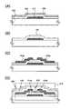
본 실시형태에서는, 액티브 매트릭스형의 액정 표시 장치의 일 예에 대해 나타낸다. 구체적으로는, 화소부에 대한 화상 신호의 입력을 선택하는 것이 가능한 액티브 매트릭스형의 액정 표시 장치에 대해 도 1(A) 및 도 1(B), 도 2, 도 3(A) 내지 도 3(C)를 참조하여 설명한다.In this embodiment, it shows about an example of an active-matrix type liquid crystal display device. Specifically, FIGS. 1 (A) and 1 (B), 2, 3 (A) to 3 (A) for an active matrix liquid crystal display device capable of selecting an input of an image signal to a pixel portion. It demonstrates with reference to C).
본 실시형태의 액정 표시 장치의 구성예에 대해 도 1(A) 및 도 1(B)를 참조하여 이하에 설명한다. 도 1(A)는, 액정 표시 장치의 구성예를 나타낸 도면이다. 도 1(A)에 나타낸 액정 표시 장치는, 제어 회로(10)와, 주사선 구동 회로(11)와, 신호선 구동 회로(12)와, 화소부(13)를 갖는다. 또한, 화소부(13)는, 매트릭스형으로 배열된 복수의 화소(14)를 갖는다. 도 1(B)는, 화소(14)의 구성예를 나타낸 도면이다. 도 1(B)에 나타낸 화소(14)는, 게이트 단자가 주사선 구동 회로(11)에 전기적으로 접속되고, 제 1 단자가 신호선 구동 회로(12)에 전기적으로 접속된 트랜지스터(15)와, 한쪽 단자가 트랜지스터(15)의 제 2 단자에 전기적으로 접속되고, 다른 한쪽 단자가 공통 전위(Vcom)를 공급하는 배선에 전기적으로 접속된 액정 소자(16)와, 한쪽 단자가 트랜지스터(15)의 제 2 단자 및 액정 소자(16)의 한쪽 단자에 전기적으로 접속되고, 다른 한쪽 단자가 공통 전위(Vcom)를 공급하는 배선에 전기적으로 접속되는 용량 소자(17)를 갖는다.The structural example of the liquid crystal display device of this embodiment is demonstrated below with reference to FIG. 1 (A) and FIG. 1 (B). FIG. 1A is a diagram illustrating a configuration example of a liquid crystal display device. The liquid crystal display device shown in FIG. 1A has a
본 실시형태의 액정 표시 장치는, 주사선 구동 회로(11)에 의해 트랜지스터(15)의 스위칭을 제어하고, 신호선 구동 회로(12)에서 트랜지스터(15)를 통해 액정 소자(16)에 화상 신호가 입력된다. 한편, 액정 소자(16)는, 한쪽 단자 및 다른 한쪽 단자에 협지된 액정층을 갖는다. 이 액정층에는 이 화상 신호와 공통 전위(Vcom)의 전위차의 전압이 인가되고, 이 전압에 의해 이 액정층의 배향 상태가 제어된다. 본 실시형태의 액정 표시 장치에서는, 이 배향을 이용하여 각 화소(14)의 표시를 제어하였다. 한편, 용량 소자(17)는, 액정 소자(16)에 인가되는 전압을 유지하기 위해 형성되어 있다.In the liquid crystal display device of this embodiment, the switching of the
나아가, 본 실시형태에 나타낸 액정 표시 장치는, 제어 회로(10)에 의해, 주사선 구동 회로(11) 및 신호선 구동 회로(12)의 동작을 제어함으로써, 화소부(13)로의 화상 신호의 입력을 선택하는 것이 가능하다.Furthermore, in the liquid crystal display device shown in this embodiment, the
이어서, 본 실시형태의 액정 표시 장치의 구성 요소의 구체 예에 대해 설명한다.Next, the specific example of the component of the liquid crystal display device of this embodiment is demonstrated.
<제어 회로(10)><
도 2는, 제어 회로(10)의 구성 예를 나타낸 도면이다. 도 2에 나타낸 제어 회로(10)는, 신호 생성 회로(20)와, 기억 회로(21)와, 비교 회로(22)와, 선택 회로(23)와, 표시 제어 회로(24)를 갖는다.2 is a diagram illustrating a configuration example of the
신호 생성 회로(20)는, 주사선 구동 회로(11) 및 신호선 구동 회로(12)를 동작시켜, 화소부(13)에 화상을 형성하기 위한 신호를 생성하는 회로이다. 구체적으로는, 화소부(13)에 매트릭스형으로 배열된 복수의 화소에 대해 입력되는 화상 신호(Data), 주사선 구동 회로(11) 또는 신호선 구동 회로(12)의 동작을 제어하는 신호(예를 들어, 스타트 펄스 신호(SP), 클럭 신호(CK) 등), 및 전원 전압인 고전원 전위(Vdd) 및 저전원 전위(Vss) 등을 생성하여, 출력하는 회로이다. 한편, 도 2에 나타낸 제어 회로(10)에서는, 신호 생성 회로(20)는, 기억 회로(21)에 대해 화상 신호(Data)를 출력하고, 표시 제어 회로(24)에 대해 주사선 구동 회로(11) 또는 신호선 구동 회로(12)의 동작을 제어하는 신호를 출력한다. 또한, 신호 생성 회로(20)에서 기억 회로(21)에 대해 출력되는 화상 신호(Data)가 아날로그 신호인 경우에는, A/D 컨버터 등을 통하여, 이 화상 신호(Data)를 디지털 신호로 변환할 수도 있다.The
기억 회로(21)는, 화소부(13)에서, 제 1 화상을 형성하기 위한 화상 신호 내지 제 n 화상(n은, 2 이상의 자연수)을 형성하기 위한 화상 신호를 기억하기 위한 복수의 메모리(25)를 갖는다. 한편, 메모리(25)는, DRAM(Dynamic Random Access Memory), SRAM(Static Random Access Memory) 등의 기억 소자를 이용하여 구성하면 된다. 또한, 메모리(25)는, 화소부(13)에서 형성되는 화상별로 화상 신호를 기억하는 구성이면 되고, 메모리(25)의 수는, 특정 수로 한정되지 않는다. 나아가, 복수의 메모리(25)가 기억하는 화상 신호는, 비교 회로(22) 및 선택 회로(23)에 의해 선택적으로 읽어진다.The
비교 회로(22)는, 기억 회로(21)에 기억된 제 k 화상(k는, 1 이상 n 미만의 자연수)을 형성하기 위한 화상 신호 및 제 k+1 화상을 형성하기 위한 화상 신호를 선택적으로 읽어, 이 화상 신호를 비교하고, 차이를 검출하는 회로이다. 한편, 제 k 화상 및 제 k+1 화상은, 화소부(13)에서 연속하여 표시되는 화상이다. 비교 회로(22)에서의 화상 신호의 비교에 의해, 차이가 검출된 경우, 이 화상 신호에 의해 형성되는 2장의 화상은 동화인 것으로 판단된다. 한편, 비교 회로(22)에서의 화상 신호의 비교에 의해, 차이가 검출되지 않은 경우, 이 화상 신호에 의해 형성되는 2장의 화상은 정지화인 것으로 판단된다. 즉, 비교 회로(22)는, 비교 회로(22)에서의 차이의 검출에 의해 연속하여 표시되는 화상을 형성하기 위한 화상 신호가, 동화를 표시하기 위한 화상 신호인지, 정지화를 표시하기 위한 화상 신호인지를 판단하는 회로이다. 한편, 비교 회로(22)는, 이 차이가 일정한 레벨을 넘었을 때에, 차이를 검출한 것으로 판단되도록 설정하여도 좋다.The
선택 회로(23)는, 비교 회로(22)에서 검출된 차이를 기초로, 화소부로의 화상 신호의 출력을 선택하는 회로이다. 구체적으로는, 선택 회로(23)는, 비교 회로(22)에서, 차이가 검출된 화상을 형성하기 위한 화상 신호는 출력하고, 차이가 검출되지 않는 화상을 형성하기 위한 화상 신호는 출력하지 않는 회로이다.The
표시 제어 회로(24)는, 스타트 펄스 신호(SP), 클럭 신호(CK), 고전원 전위(Vdd), 및 저전원 전위(Vss) 등의 제어 신호의 주사선 구동 회로(11) 및 신호선 구동 회로(12)로의 공급을 제어하는 회로이다. 구체적으로는, 비교 회로(22)에 의해 동화로 판단된 경우(연속하여 표시되는 화상에 차이가 검출된 경우)에는, 선택 회로(23)에서 공급된 화상 신호(Data)를 신호선 구동 회로(12)에 출력함과 동시에, 주사선 구동 회로(11) 및 신호선 구동 회로(12)에 대해, 제어 신호(스타트 펄스 신호(SP), 클럭 신호(CK), 고전원 전위(Vdd), 및 저전원 전위(Vss) 등)을 공급한다. 한편, 비교 회로(22)에 의해 정지화로 판단된 경우(연속하여 표시되는 화상에 차이가 검출되지 않는 경우)에는, 선택 회로(23)에서 화상 신호(Data)가 공급되지 않는 동시에, 주사선 구동 회로(11) 및 신호선 구동 회로(12)에 대해, 제어 신호(스타트 펄스 신호(SP), 클럭 신호(CK), 고전원 전위(Vdd), 및 저전원 전위(Vss) 등)을 공급하지 않는다. 즉, 비교 회로(22)에 의해 정지화로 판단된 경우(연속하여 표시되는 화상에 차이가 검출되지 않는 경우)에는, 주사선 구동 회로(11) 및 신호선 구동 회로(12)의 동작을 완전히 정지시킨다. 단, 정지화로 판단되는 기간이 짧은 경우에는, 고전원 전위(Vdd) 및 저전원 전위(Vss)를 계속 공급하는 구성으로 할 수도 있다. 한편, 고전원 전위(Vdd) 및 저전원 전위(Vss)가 공급되는 것이란, 어느 배선의 전위가 고전원 전위(Vdd) 또는 저전원 전위(Vss)에 고정되는 것이다. 즉, 어느 전위 상태에 있는 이 배선이, 고전원 전위(Vdd) 또는 저전원 전위(Vss)로 변화하게 된다. 당연히, 이 전위의 변화에는 전력 소비가 수반된다. 이로 인해, 빈번하게 고전원 전위(Vdd) 및 저전원 전위(Vss)의 공급 정지 및 재공급을 행함으로써, 결과적으로, 소비 전력이 증대될 가능성이 있다. 이와 같은 경우에는, 고전원 전위(Vdd) 및 저전원 전위(Vss)를 계속 공급하는 구성으로 하는 것이 바람직하다. 한편, 상기한 설명에서, 신호를 '공급하지 않는다'란, 이 신호를 공급하는 배선에서 소정의 전위와는 다른 전위가 공급되는, 또는 이 배선의 전위가 부유 상태가 되는 것을 말하는 것으로 한다.The
제어 회로(10)에서, 상기한 바와 같이 주사선 구동 회로(11) 및 신호선 구동 회로(12)의 동작을 제어함으로써 액정 표시 장치의 소비 전력을 저감하는 것이 가능하다.In the
<트랜지스터(15)><
트랜지스터(15)는, 채널 형성 영역이 산화물 반도체층에 의해 구성되는 트랜지스터이다. 이 산화물 반도체층은, 전기적 특성 변동을 억지하기 위해, 변동 요인이 되는 수소, 수분, 수산기 또는 수소화물(수소 화합물이라고도 한다) 등의 불순물을 의도적으로 배제하고, 또한 불순물의 배제 공정에 의해 동시에 감소하게 되는 산화물 반도체를 구성하는 주성분 재료인 산소를 공급함으로써, 고순도화 및 전기적으로 I형(진성)화된 산화물 반도체층이다. 한편, 이 산화물 반도체는, 2eV 이상, 바람직하게는 2.5eV 이상, 더욱 바람직하게는 3.0eV 이상의 밴드갭을 갖는다.The
또한, 고순도화된 산화물 반도체 중에는 캐리어가 매우 작고(0에 가까움), 캐리어 밀도는 1×10¹⁴/cm3 미만, 바람직하게는 1×10¹²/cm3 이하이다. 즉, 산화물 반도체층의 캐리어 밀도는, 무한대로 0으로 한다. 산화물 반도체층 중에 캐리어가 매우 적으므로, 오프 전류값을 낮게 할 수 있다. 오프 전류값은 낮으면 낮을수록 바람직하다. 이로 인해, 상기한 트랜지스터에서는, 채널 폭(w)이 1㎛당 실온에서의 오프 전류값을 10aA/㎛(1×10-17A/㎛) 이하로 하는 것, 및 85℃에서의 오프 전류값을 100aA/㎛(1×10-16A/㎛) 이하로 하는 것이 가능하다. 한편, 일반적으로, 아몰퍼스 실리콘을 구비하는 트랜지스터에서는, 실온에서의 오프 전류값은 1×10-13A/㎛ 이상이 된다. 또한, pn 접합이 없고, 핫캐리어 열화가 없으므로, 이들에 트랜지스터의 전기적 특성이 영향을 받지 않는다. 이에 의해, 각 화소(14)의 화상 신호의 유지 기간을 길게 할 수 있다. 즉, 정지화를 표시할 때의 화상 신호의 다시 쓰기의 간격을 길게 할 수 있다. 예를 들어, 화상 신호의 쓰기 간격을 10초 이상, 바람직하게는 30초 이상, 더욱 바람직하게는 1분 이상 10분 미만으로 할 수 있다. 쓰기 간격을 길게 하면, 소비 전력을 억제하는 효과를 높일 수 있다.In addition, in highly purified oxide semiconductors, the carrier is very small (close to zero), and the carrier density is less than 1 × 10¹⁴ / cm3 , preferably 1 × 10¹² / cm3 or less. That is, the carrier density of the oxide semiconductor layer is set to zero at infinity. Since there are very few carriers in an oxide semiconductor layer, an off current value can be made low. The lower the off current value is, the better. For this reason, in the transistor described above, the channel current width w is set to 10 aA / μm (1 × 10-17 A / μm) or less at room temperature per 1 μm, and the off current value at 85 ° C. It is possible to set it to 100aA / micrometer (1x10 <-16> A / micrometer) or less. On the other hand, in a transistor including amorphous silicon, on the other hand, the off current value at room temperature is 1 × 10⁻¹³ A / μm or more. In addition, since there is no pn junction and no hot carrier degradation, the electrical characteristics of the transistor are not affected by these. Thereby, the holding period of the image signal of each
한편, 트랜지스터의 오프 전류가 흐르기 어려운 정도를 오프 저항율로 나타낼 수 있다. 오프 저항율이란, 트랜지스터가 오프일 때의 채널 형성 영역의 저항율이고, 오프 저항율은 오프 전류에서 산출할 수 있다.On the other hand, the degree of difficulty in flowing off current of the transistor can be represented by the off resistance. The off resistivity is the resistivity of the channel formation region when the transistor is off, and the off resistivity can be calculated from the off current.
구체적으로는, 오프 전류와 드레인 전압의 값을 알면 옴의 법칙으로 트랜지스터가 오프일 때의 저항값(오프 저항(R))을 산출할 수 있다. 그리고 채널 형성 영역의 단면적(A)과 채널 형성 영역의 길이(소스 드레인 전극 간의 거리에 상당)(L)를 알면 ρ=RA/L의 식(R은 오프 저항)에서 오프 저항율(ρ)을 산출할 수 있다.Specifically, by knowing the values of the off current and the drain voltage, the ohmic law can calculate the resistance value (off resistance R) when the transistor is off. Knowing the cross-sectional area A of the channel formation region and the length of the channel formation region (corresponding to the distance between the source and drain electrodes) L, the off resistivity ρ is calculated from the equation ρ = RA / L (R is off resistance). can do.
여기서, 단면적(A)은, 채널 형성 영역의 막후를 d로 하고, 채널 폭을 W로 할 때, A=dW에서 산출할 수 있다. 또한, 채널 형성 영역의 길이(L)는 채널 길이(L)이다. 이상과 같이, 오프 전류에서 오프 저항율을 산출할 수 있다.Here, the cross-sectional area A can be calculated at A = dW when the film thickness of the channel formation region is d and the channel width is W. In addition, the length L of the channel formation region is the channel length L. FIG. As described above, the off resistivity can be calculated from the off current.
본 실시형태의 산화물 반도체층을 구비하는 트랜지스터의 오프 저항율은 1×10¹¹Ω·cm 이상이 바람직하고, 나아가 1×10¹²Ω·cm 이상이 더욱 바람직하다.The off resistivity of the transistor including the oxide semiconductor layer of the present embodiment is preferably 1 × 10¹¹ Ω · cm or more, more preferably 1 × 10¹² Ω · cm or more.
이와 같이 산화물 반도체층에 포함되는 수소를 철저히 제거함으로써 고순도화된 산화물 반도체층을 트랜지스터의 채널 형성 영역으로 이용한 트랜지스터는, 오프 전류값을 매우 낮게 할 수 있다. 즉, 트랜지스터가 오프 상태에 있을 때, 산화물 반도체층을 절연체로 간주하여 회로 설계를 할 수 있다. 한편, 산화물 반도체층을 구비하는 트랜지스터는, 온 상태에서는, 아몰퍼스 실리콘층을 구비하는 트랜지스터보다도 높은 전류 공급 능력을 가질 수 있다.Thus, the transistor which used the highly purified oxide semiconductor layer as the channel formation area of a transistor by thoroughly removing hydrogen contained in an oxide semiconductor layer can make an off current value very low. That is, when the transistor is in the off state, the circuit design can be performed by considering the oxide semiconductor layer as an insulator. On the other hand, the transistor including the oxide semiconductor layer can have a higher current supply capability than the transistor including the amorphous silicon layer in the on state.
또한, 저온 폴리 실리콘층을 구비하는 트랜지스터에서는, 산화물 반도체층을 구비하는 트랜지스터와 비교하여, 실온에서의 오프 전류값이 10000배 정도 큰 값인 것으로 상정하여 설계 등을 하였다. 이로 인해, 산화물 반도체층을 구비하는 트랜지스터에서는, 저온 폴리 실리콘층을 구비하는 트랜지스터에 비해, 유지 용량이 동등(0.1pF 정도)할 때, 전압의 유지 기간을 10000배 정도로 연장할 수 있다. 일 예로, 동화 표시를 매초 60프레임으로 행하는 경우, 1회의 신호 쓰기에 의한 유지 기간을 10000배인 160초 정도로 할 수 있다. 그리고, 적은 화상 신호의 쓰기 횟수로도, 표시부에서의 정지화의 표시를 행할 수 있다.In addition, in the transistor provided with a low temperature polysilicon layer, compared with the transistor provided with an oxide semiconductor layer, it assumed that the off-current value at room temperature is about 10000 times larger, and designed. For this reason, in the transistor provided with the oxide semiconductor layer, when the holding capacitance is equivalent (about 0.1 pF), the sustain period of the voltage can be extended to about 10,000 times as compared with the transistor having the low temperature polysilicon layer. For example, when moving pictures are displayed at 60 frames per second, the sustain period by one signal write can be about 160 seconds, which is 10000 times. The still image display on the display section can be performed even with a small number of times of writing of image signals.
유지 기간을 길게 함으로써, 화소로의 화상 신호의 공급을 행하는 빈도를 저감할 수 있다. 특히, 상기한 바와 같은, 화상 신호를 선택적으로 화소부에 입력하는 것이 가능한 액정 표시 장치에 대해서는, 상기한 트랜지스터를 적용하는 효과가 크다. 즉, 이 액정 표시 장치에서는, 장기간에 걸쳐 화상 신호가 화소에 입력되지 않을 가능성이 있으나, 상기한 트랜지스터를 화소로의 화상 신호의 입력을 제어하는 트랜지스터로 적용함으로써, 이 화소의 표시의 열화(변화)를 억제할 수 있다.By lengthening the sustain period, the frequency of supplying the image signal to the pixels can be reduced. In particular, for the liquid crystal display device capable of selectively inputting the image signal to the pixel portion as described above, the effect of applying the above-described transistor is great. That is, in this liquid crystal display device, there is a possibility that an image signal may not be inputted to a pixel for a long time, but deterioration (change) of the display of the pixel is applied by applying the above-described transistor to a transistor that controls the input of the image signal to the pixel. ) Can be suppressed.
또한, 이 트랜지스터를 화소로의 화상 신호의 입력을 제어하는 스위치로 적용함으로써, 화소에 형성되는 용량 소자의 사이즈를 축소하는 것이 가능해진다. 이에 의해, 이 화소의 개구율을 향상시키는 것 및 이 화소로의 화상 신호의 입력을 고속으로 행하는 것 등이 가능해진다.Further, by applying this transistor as a switch for controlling the input of an image signal to a pixel, it becomes possible to reduce the size of the capacitor formed in the pixel. This makes it possible to improve the aperture ratio of the pixel, to input the image signal to the pixel at high speed, and the like.
<액정 소자(16) 및 용량 소자(17)><
화상 신호의 입력을 제어하는 트랜지스터(15)로 상기한 트랜지스터를 적용하는 경우, 액정 소자(16)가 갖는 액정 재료로 고유 저항율이 높은 물질을 적용하는 것이 바람직하다. 여기서, 도 3(A) 내지 도 3(C)를 참조하여 그 이유에 대해 설명한다. 한편, 도 3(A) 내지 도 3(C)는, 아몰퍼스 실리콘층을 구비하는 트랜지스터를 갖는 화소 및 상기 산화물 반도체층을 구비하는 트랜지스터를 갖는 화소에서의 화상 신호의 리크 경로를 나타낸 모식도이다.When the above-described transistor is applied to the
도 1(B)에 나타낸 바와 같이, 이 화소는, 트랜지스터(15)와, 액정 소자(16)와, 용량 소자(17)에 의해 구성되고, 트랜지스터(15)가 오프 상태에 있는 경우, 도 3(A)에 나타낸 회로와 등가이다. 즉, 트랜지스터(15)를 저항(RTr-Off)에 의해 나타내고, 액정 소자(16)를 저항(RLC) 및 용량 (CLC)에 의해 나타낸 회로와 등가이다. 화상 신호가 이 화소에 입력되면, 이 화상 신호는, 용량 소자(17)의 용량 (CS) 및 액정 소자(16)의 용량(CLC)에 저장된다. 그 후, 트랜지스터(15)가 오프 상태가 되면, 도 3(B), (C)에 나타낸 바와 같이 트랜지스터(15) 및 액정 소자(16)를 통해, 화상 신호가 리크된다. 한편, 도 3(B)는, 트랜지스터(15)가 아몰퍼스 실리콘층을 구비하는 트랜지스터인 경우의 화상 신호의 리크를 나타낸 모식도이고, 도 3(C)는, 트랜지스터(15)가 산화물 반도체층을 구비하는 트랜지스터인 경우의 화상 신호의 리크를 나타낸 모식도이다. 아몰퍼스 실리콘층을 구비하는 트랜지스터의 오프 저항값은, 액정 소자의 저항값보다 낮다. 이로 인해, 도 3(B)에 나타낸 바와 같이, 화상 신호의 리크는, 아몰퍼스 실리콘층을 구비하는 트랜지스터를 통한 리크가 주가 된다(도 3(B) 중, 경로(A) 및 경로(B)를 거친 리크가 주가 된다). 한편, 고순도화된 산화물 반도체층을 구비하는 트랜지스터의 오프 저항값은, 액정 소자의 저항값보다 높다. 이로 인해, 도 3(C)에 나타낸 바와 같이, 화상 신호의 리크는, 액정 소자를 통한 리크가 주가 된다(도 3(C), 경로(C) 및 경로(D)를 거친 리크가 주가 된다).As shown in FIG. 1B, this pixel is composed of a
즉, 종래에서는, 액정 표시 장치의 각 화소에서의 화상 신호의 유지 특성은, 각 화소에 형성되는 트랜지스터의 특성을 율속점으로 하였으나, 고순도화된 산화물 반도체층을 구비하는 트랜지스터를 각 화소에 형성되는 트랜지스터에 적용함으로써, 액정 소자의 저항값이 율속점이 된다. 이로 인해, 액정 소자(16)가 갖는 액정 재료로 고유 저항율이 높은 물질을 적용하는 것이 바람직하다.That is, in the related art, the holding characteristic of the image signal in each pixel of the liquid crystal display device is that the characteristics of the transistors formed in each pixel are set at the rate point, but transistors having a highly purified oxide semiconductor layer are formed in each pixel. By applying to a transistor, the resistance value of a liquid crystal element becomes a rate speed point. For this reason, it is preferable to apply the substance with high intrinsic resistivity to the liquid crystal material which the
구체적으로는, 화소에, 고순도화된 산화물 반도체층을 구비하는 트랜지스터를 갖는 액정 표시 장치에서는, 액정 재료의 고유 저항율은, 1×10¹²Ω·cm 이상이고, 바람직하게는 1×10¹³Ω·cm를 넘는 것이고, 더욱 바람직하게는 1×10¹⁴Ω·cm를 넘는 것이 바람직한 요건이 된다. 한편, 이 액정 재료를 이용하여 액정 소자를 구성한 경우의 저항은, 배향막 및 씰재로부터의 불순물이 혼입될 가능성도 있고, 1×10¹¹Ω·cm 이상이고, 더욱 바람직하게는 1×10¹²Ω·cm를 넘는 것이 바람직한 요건이 된다. 또한, 본 명세서에서의 고유 저항율의 값은, 20℃에서 측정한 값으로 한다.Specifically, in a liquid crystal display device having a transistor including a high purity oxide semiconductor layer in a pixel, the resistivity of the liquid crystal material is 1 × 10¹² Ω · cm or more, preferably 1 × 10¹³ Ω · It is more than cm, More preferably, more than 1 x 10¹⁴ Ωcm is a preferred requirement. On the other hand, in the case where the liquid crystal element is formed using this liquid crystal material, the impurities from the alignment film and the sealing material may be mixed, and the resistance is 1 × 10¹¹ Ω · cm or more, more preferably 1 × 10¹² Ω · More than cm is a desirable requirement. In addition, the value of the specific resistivity in this specification shall be the value measured at 20 degreeC.
또한, 정지화 표시에서의 유지 기간에서, 액정 소자(16)의 다른 한쪽 단자로의 공통 전위(Vcom)의 공급을 하지 않고, 이 단자를 부유 상태로 할 수도 있다. 구체적으로는, 이 단자와, 공통 전위(Vcom)를 공급하는 전원 사이에 스위치를 구비하고, 쓰기 기간 중에는 스위치를 온으로 하여 전원에서 공통 전위(Vcom)를 공급한 후, 남은 유지 기간에서는 스위치를 오프로 하여 부유 상태로 하면 된다. 이 스위치에 대해서도, 상기 고순도화된 산화물 반도체층을 구비하는 트랜지스터를 이용하는 것이 바람직하다. 액정 소자(16)의 다른 한쪽 단자를 부유 상태로 함으로써, 부정 펄스 등에 의한, 화소(14)에서의 표시의 열화(변화)를 저감할 수 있다. 왜냐하면, 트랜지스터(15)가 오프 상태에 있는 경우에 트랜지스터(15)의 제 1 단자의 전위가 부정 펄스에 의해 변동하면, 용량 결합에 의해 액정 소자(16)의 한쪽 단자의 전위도 변동한다. 이때, 액정 소자(16)의 다른 한쪽 단자에 공통 전위(Vcom)가 공급된 상태라면, 이 변동은 액정 소자(16)에 인가되는 전압치의 변화에 직결되는데 반해, 액정 소자의 다른 한쪽 단자가 부유 상태에 있으면, 이 단자의 전위도 용량 결합에 의해 변동한다. 이로 인해, 트랜지스터(15)의 제 1 단자의 전위가 부정 펄스에 의해 변동한 경우라도, 액정 소자(16)에 인가되는 전압치의 변화를 저감할 수 있고, 화소(14)에서의 표시의 열화(변화)를 저감할 수 있다.Further, in the sustain period in the still display, the terminal can be left in a floating state without supplying the common potential Vcom to the other terminal of the
또한, 용량 소자(17)의 용량(CS)의 크기는, 각 화소에 형성된 트랜지스터의 오프 전류 등을 고려하여 설정되는 것이다. 단, 상기한 바와 같이, 고순도화된 산화물 반도체층을 구비하는 트랜지스터를 화소가 갖는 트랜지스터에 적용함으로써, 용량 소자(17)의 설계에 요구되는 조건이 크게 변화한다. 이하에 구체적인 수치를 들어 이 내용에 대해 설명한다.The size of the capacitor CS of the
일반적으로 화소가 갖는 트랜지스터로 아몰퍼스 실리콘층을 구비하는 트랜지스터를 적용한 경우의 오프 저항값은, 1×10¹²Ω 정도이고, 액정 소자의 저항값은 1×10¹⁵Ω 정도이다. 이로 인해, 화소가 갖는 트랜지스터를 고순도화된 산화물 반도체층을 구비하는 트랜지스터로 함으로써, 이 화소에서의 화상 신호의 리크를 1/1000 정도까지 저감하는 것이 가능하다. 즉, 용량 소자(17)의 용량(CS)의 크기를 1/1000 정도까지 저감하는 것, 또는 이 화소에서 정지화를 표시하는 경우의 화상 신호의 다시 쓰기의 빈도를 1/1000 정도까지 저감할 수 있다. 예를 들어, 1초 동안 60회의 화상 신호의 쓰기를 하는 경우는, 15초 동안 1회 정도까지 이 쓰기의 빈도를 저감하는 것이 가능하다. 또한, 용량 소자(17)로, 50fF 정도의 용량을 갖는 소자를 적용함으로써, 화소에서 화상 신호를 30초 정도 유지할 수 있다. 일 예로, 각 화소에서 화상 신호를 5초 이상 5분 이하로 유지하기 위해서는, 용량 소자(17)의 용량(CS)이 0.5pF 이상인 것이 바람직하고, 1pF 이상인 것이 더욱 바람직하다. 한편, 상기한 설명에서의 각종 수치는, 대략 계산한 값인 것을 밝혀둔다.In general, the off-resistance value in the case of applying a transistor having an amorphous silicon layer as the transistor of the pixel is about 1 × 10¹² Ω, and the resistance value of the liquid crystal element is about 1 × 10¹⁵ Ω. For this reason, by making the transistor which a pixel has a highly purified oxide semiconductor layer, the leak of the image signal in this pixel can be reduced to about 1/1000. That is, reducing the size of the capacitor CS of the
한편, 본 실시형태의 내용 또는 이 내용의 일부는, 다른 실시형태의 내용 또는 이 내용의 일부 또는 실시예의 내용 또는 이 내용의 일부와 자유롭게 조합하는 것이 가능하다.
In addition, the content of this embodiment or a part of this content can be combined freely with the content of another embodiment, a part of this content, the content of an Example, or a part of this content.
(실시형태 2)(Embodiment 2)
본 실시형태에서는, 실시형태 1에 나타낸 트랜지스터의 일 예에 대해 도 4(A)~(D)를 참조하여 설명한다.In this embodiment, an example of the transistor shown in Embodiment 1 will be described with reference to FIGS. 4A to 4D.
도 4(A)~(D)는, 실시형태 1에 나타낸 트랜지스터의 구체적인 구성 및 제작 공정의 구체예를 나타낸 도면이다. 한편, 도 4(A)~(D)에 나타낸 박막 트랜지스터(410)는, 채널 에치형이라 불리는 보톰 게이트 구조의 하나로, 역스태거형 박막 트랜지스터라고도 한다. 또한, 도 4(A)~(D)에는, 싱글 게이트 구조의 박막 트랜지스터를 나타내나, 필요에 따라, 채널 형성 영역을 복수 갖는 멀티 게이트 구조의 박막 트랜지스터로 할 수 있다.4 (A) to (D) are diagrams showing specific examples of the specific configuration and manufacturing process of the transistor shown in the first embodiment. On the other hand, the
이하, 도 4(A)~(D)를 참조하여, 기판(400) 위에 박막 트랜지스터(410)를 제작하는 공정에 대해 설명한다.Hereinafter, a process of manufacturing the
우선, 절연 표면을 갖는 기판(400) 위에 도전막을 형성한 후, 제 1 포토리소 그래피 공정에 의해 게이트 전극층(411)을 형성한다. 한편, 이 공정에서 이용되는 레지스트 마스크는, 잉크젯법에 의해 형성하여도 좋다. 레지스트 마스크를 잉크젯법으로 형성하면 포토 마스크를 사용하지 않으므로, 제조 비용을 저감할 수 있다.First, after forming a conductive film on the
절연 표면을 갖는 기판(400)에 사용할 수 있는 기판에 큰 제한은 없으나, 적어도, 후의 가열 처리에 견딜 수 있는 정도의 내열성을 가질 필요가 있다. 예를 들어, 바륨 붕규산 유리나 알루미노 붕규산 유리 등의 유리 기판을 이용할 수 있다. 또한, 유리 기판으로는, 후의 가열 처리의 온도가 높은 경우에는, 변형점이 730℃ 이상인 것을 이용하는 것이 좋다.Although there is no big restriction | limiting in the board | substrate which can be used for the board |
하지막이 되는 절연막을 기판(400)과 게이트 전극층(411) 사이에 형성하여도 좋다. 하지막은, 기판(400)에서의 불순물 원소의 확산을 방지하는 기능이 있고, 질화 실리콘막, 산화 실리콘막, 질화산화 실리콘막, 또는 산화질화 실리콘막에서 선택된 하나 또는 복수의 막에 의한 적층 구조에 의해 형성할 수 있다.An insulating film serving as a base film may be formed between the
또한, 게이트 전극층(411)의 재료는, 몰리브덴, 티탄, 크롬, 탄탈, 텅스텐, 알루미늄, 구리, 네오디뮴, 스칸듐 등의 금속 재료 또는 이를 주성분으로 하는 합금 재료를 이용하여, 단층 또는 적층하여 형성할 수 있다.The material of the
예를 들어, 게이트 전극층(411)의 2층의 적층 구조로는, 알루미늄층 위에 몰리브덴층을 적층한 2층 구조, 구리층 위에 몰리브덴층을 적층한 2층 구조, 구리층 위에 질화 티탄층 또는 질화 탄탈을 적층한 2층 구조, 질화 티탄층과 몰리브덴층을 적층한 2층 구조로 하는 것이 바람직하다. 3층의 적층 구조로는, 텅스텐층 또는 질화 텅스텐층과, 알루미늄과 실리콘의 합금층 또는 알루미늄과 티탄의 합금층과, 질화 티탄층 또는 티탄층을 적층한 3층 구조로 하는 것이 바람직하다.For example, as a two-layer laminated structure of the
이어서, 게이트 전극층(411) 위에 게이트 절연층(402)을 형성한다.Subsequently, a
게이트 절연층(402)은, 플라즈마 CVD법 또는 스퍼터링법 등을 이용하여, 산화 실리콘층, 질화 실리콘층, 산화질화 실리콘층, 질화산화 실리콘층, 또는 산화 알루미늄층을 단층 또는 적층하여 형성할 수 있다. 예를 들어, 성막 가스로, 실란(SiH4), 산소 및 질소를 이용하여 플라즈마 CVD법에 의해 산화질화 실리콘층을 형성하면 된다. 또한, 게이트 절연층으로 산화 하프늄(HfOx), 산화탄탈(TaOx) 등의 High-k 재료를 이용할 수도 있다. 게이트 절연층(402)의 막후는, 100nm 이상 500nm 이하로 하고, 적층의 경우는, 예를 들어, 막후 50nm 이상 200nm 이하의 제 1 게이트 절연층과, 제 1 게이트 절연층 위에 막후 5nm 이상 300nm 이하의 제 2 게이트 절연층을 적층하여 형성한다.The
여기서는, 게이트 절연층(402)으로 플라즈마 CVD법에 의해 막후 100nm 이하의 산화질화 실리콘층을 형성한다.Here, as the
또한, 게이트 절연층(402)으로, 고밀도 플라즈마 장치를 이용하여, 산화질화 실리콘막을 형성하여도 좋다. 여기서 고밀도 플라즈마 장치란, 1×10¹¹/cm3 이상의 플라즈마 밀도를 달성할 수 있는 장치를 말한다. 예를 들어, 3kW~6kW의 마이크로파 전력을 인가하여 플라즈마를 발생시켜, 절연막을 성막한다.As the
챔버에 재료 가스로 실란(SiH4), 아산화질소(N2O), 및 희가스를 도입하고, 10Pa~30Pa의 압력 하에서 고밀도 플라즈마를 발생시켜 유리 등의 절연 표면을 갖는 기판 위에 절연막을 형성한다. 그 후, 실란(SiH4)의 공급을 정지하고, 대기에 노출시키지 않고 아산화질소(N2O)와 희가스를 도입하여 절연막 표면에 플라즈마 처리를 하여도 좋다. 적어도 아산화질소(N2O)와 희가스를 도입하여 절연막 표면에 이루어지는 플라즈마 처리는, 절연막의 성막보다 나중에 행한다. 상기 프로세스 순서를 거친 절연막은, 막후가 얇고, 예를 들어 100nm 미만이라도 신뢰성을 확보할 수 있는 절연막이다.Silane (SiH4 ), nitrous oxide (N2 O), and rare gas are introduced into the chamber as a material gas, and a high density plasma is generated under a pressure of 10 Pa to 30 Pa to form an insulating film on a substrate having an insulating surface such as glass. Thereafter, the supply of silane (SiH4 ) may be stopped and plasma treatment may be performed on the surface of the insulating film by introducing nitrous oxide (N2 O) and a rare gas without exposing to the atmosphere. Plasma processing performed on the surface of the insulating film by introducing at least nitrous oxide (N2 O) and a rare gas is performed later than film formation of the insulating film. The insulating film which has passed through the above-described process procedure is an insulating film which is thin in thickness and can ensure reliability even if it is less than 100 nm, for example.
게이트 절연층(402)의 형성 시, 챔버에 도입하는 실란(SiH4)과 아산화질소(N2O)의 유량비는, 1:10에서 1:200의 범위로 한다. 또한, 챔버에 도입하는 희가스로는, 헬륨, 아르곤, 클립톤, 크세논 등을 이용할 수 있으나, 그 중에서도 저렴한 아르곤을 이용하는 것이 바람직하다.At the time of forming the
또한, 고밀도 플라즈마 장치에 의해 얻어진 절연막은, 일정한 두께의 막 형성이 가능하므로 단차 피복성이 우수하다. 또한, 고밀도 플라즈마 장치에 의해 얻어진 절연막은, 얇은 막의 두께를 정밀하게 제어할 수 있다.Moreover, since the insulating film obtained by the high density plasma apparatus can form a film of fixed thickness, it is excellent in step coverage. In addition, the insulating film obtained by the high density plasma apparatus can precisely control the thickness of the thin film.
상기 프로세스 순서를 거친 절연막은, 종래의 평행평판형 PCVD장치에서 얻어지는 절연막과는 크게 다르며, 동일한 에천트를 이용하여 에칭 속도를 비교한 경우에서, 평행평판형 PCVD 장치에서 얻어지는 절연막의 10% 이상 또는 20% 이상 느리며, 고밀도 플라즈마 장치에서 얻어지는 절연막은 치밀한 막이라 할 수 있다.The insulating film that has undergone the above process procedure is significantly different from the insulating film obtained in the conventional parallel flat PCVD apparatus, and when the etching rates are compared using the same etchant, 10% or more of the insulating film obtained in the parallel flat PCVD apparatus or It is slower than 20%, and the insulating film obtained in the high density plasma apparatus is a dense film.
한편, 후의 공정에서 i형화 또는 실질적으로 i형화된 산화물 반도체층(고순도화된 산화물 반도체층)은 계면 준위, 계면 전하에 대해 매우 민감하므로, 게이트 절연층과의 계면은 중요하다. 이로 인해 고순도화된 산화물 반도체층에 접하는 게이트 절연층은, 고품질화가 요구된다. 따라서 μ파(2.45GHz)를 이용한 고밀도 플라즈마 CVD 장치는, 치밀하고 절연 내압이 높은 고품질의 절연막을 형성할 수 있으므로 바람직하다. 고순도화된 산화물 반도체층과 고품질 게이트 절연층이 밀접함으로써, 계면 준위를 저감하여 계면 특성을 양호한 것으로 할 수 있기 때문이다. 게이트 절연층으로써 막질이 양호한 것은 물론, 산화물 반도체층과의 계면 준위 밀도를 저감하고, 양호한 계면을 형성할 수 있는 것이 중요하다.On the other hand, since the i-typed or substantially i-typed oxide semiconductor layer (highly purified oxide semiconductor layer) is very sensitive to the interface level and the interface charge in a later step, the interface with the gate insulating layer is important. For this reason, the gate insulating layer in contact with the highly purified oxide semiconductor layer is required to be of high quality. Therefore, a high-density plasma CVD apparatus using μ wave (2.45 GHz) is preferable because it can form a high quality insulating film with high density and high dielectric breakdown voltage. This is because the high purity oxide semiconductor layer and the high quality gate insulating layer are in close contact, whereby the interface level can be reduced and the interface characteristics can be made good. It is important not only that the film quality is good as the gate insulating layer, but also that the density of the interface state with the oxide semiconductor layer can be reduced and a good interface can be formed.
이어서, 게이트 절연층(402) 위에, 막후 2nm 이상 200nm 이하의 산화물 반도체막(430)을 형성한다. 한편, 산화물 반도체막(430)을 스퍼터링법에 의해 성막하기 전에, 아르곤 가스를 도입하여 플라즈마를 발생시키는 역스퍼터링을 행하고, 게이트 절연층(402)의 표면에 부착되어 있는 가루형 물질(파티클, 먼지라고도 한다)을 제거하는 것이 바람직하다. 역스퍼터링이란, 타겟 측으로 전압을 인가하지 않고, 아르곤 분위기 하에서 기판 측으로 RF 전원을 이용하여 전압을 인가하여 기판에 플라즈마를 형성하여 표면을 개질하는 방법이다. 한편, 아르곤 분위기 대신 질소, 헬륨, 산소 등을 이용하여도 좋다. Subsequently, an
산화물 반도체막(430)은, In-Ga-Zn-O계, In-Sn-O계, In-Sn-Zn-O계, In-Al-Zn-O계, Sn-Ga-Zn-O계, Al-Ga-Zn-O계, Sn-Al-Zn-O계, In-Zn-O계, Sn-Zn-O계, Al-Zn-O계, In-O계, Sn-O계, Zn-O계의 산화물 반도체막을 이용한다. 본 실시형태에서는, 산화물 반도체막(430)으로, In-Ga-Zn-O계 금속 산화물 타겟을 이용하여 스퍼터링법에 의해 성막한다. 이 단계에서의 단면도가 도 4(A)에 상당한다. 또한, 산화물 반도체막(430)은, 희가스(대표적으로는 아르곤) 분위기 하, 산소 분위기 하, 또는 희가스(대표적으로는 아르곤) 및 산소의 혼합 분위기 하에서 스퍼터링법에 의해 형성할 수 있다. 또한, 스퍼터링법을 이용하는 경우, SiO2를 2중량% 이상 10중량% 이하 포함하는 타겟을 이용하여 성막하고, 산화물 반도체막(430)에 결정화를 저해하는 SiOx(X>0)를 포함시켜, 후의 공정에서 행하는 탈수화 또는 탈수소화를 위한 가열 처리 시에 결정화되어 버리는 것을 억제할 수 있다.The
여기서는, In, Ga, 및 Zn을 포함하는 금속 산화물 타겟(In2O3:Ga2O3:ZnO=1:1:1[mol], In:Ga:Zn=1:1:0.5[atom])을 이용하여, 기판과 타겟 사이의 거리를 100mm, 압력 0.2Pa, 직류(DC) 전원 0.5kW, 아르곤 및 산소(아르곤:산소=30sccm:20sccm, 산소 유량 비율 40%) 분위기 하에서 성막한다. 한편, 펄스 직류(DC) 전원을 이용하면, 성막 시에 발생하는 가루형 물질을 경감할 수 있고, 막후 분포도 균일해지므로 바람직하다. In-Ga-Zn-O계 막의 막후는, 5nm 이상 200nm 이하로 한다. 본 실시형태에서는, 산화물 반도체막으로, In-Ga-Zn-O계 금속 산화물 타겟을 이용하여 스퍼터링법에 의해 막후 20nm의 In-Ga-Zn-O계 막을 성막한다. 또한, In, Ga, 및 Zn을 포함하는 금속 산화물 타겟으로, In:Ga:Zn=1:1:1[atom], 또는 In:Ga:Zn=1:1:2[atom]의 조성비를 갖는 타겟을 이용할 수도 있다.Here, a metal oxide target containing In, Ga, and Zn (In2 O3 : Ga2 O3 : ZnO = 1: 1: 1 [mol], In: Ga: Zn = 1: 1: 0.5 [atom] ) Is formed under a 100 mm, pressure 0.2 Pa, 0.5 kW direct current (DC) power supply, argon and oxygen (argon: oxygen = 30 sccm: 20 sccm, oxygen flow rate ratio 40%). On the other hand, when a pulsed direct current (DC) power supply is used, the powdery substance which arises at the time of film-forming can be reduced, and since post-film distribution becomes uniform, it is preferable. The thickness of the In-Ga-Zn-O-based film is set to 5 nm or more and 200 nm or less. In this embodiment, an In-Ga-Zn-O based film having a thickness of 20 nm is formed by sputtering using an In—Ga—Zn—O based metal oxide target as the oxide semiconductor film. Further, a metal oxide target containing In, Ga, and Zn, which has a composition ratio of In: Ga: Zn = 1: 1: 1 [atom], or In: Ga: Zn = 1: 1: 2 [atom]. You can also use a target.
스퍼터링법에는 스퍼터링용 전원에 고주파 전원을 이용하는 RF 스퍼터링법과 DC 스퍼터링법이 있고, 또한 펄스적으로 바이어스를 가하는 펄스 DC 스퍼터링법도 있다. RF 스퍼터링법은 주로 절연막을 성막하는 경우에 이용되고, DC 스퍼터링법은 주로 금속막을 성막하는 경우에 이용된다.As the sputtering method, there are an RF sputtering method and a DC sputtering method using a high frequency power source for the sputtering power supply, and there is also a pulsed DC sputtering method in which pulses are biased. The RF sputtering method is mainly used for forming an insulating film, and the DC sputtering method is mainly used for forming a metal film.
또한, 재료가 다른 타겟을 복수할 수 있는 다원 스퍼터링 장치도 있다. 다원 스퍼터링 장치는, 동일 챔버에서 다른 재료막을 적층 성막할 수도, 동일 챔버에서 복수 종류의 재료를 동시에 방전시켜 성막할 수도 있다. There is also a multiple sputtering device capable of plural targets having different materials. The multiple sputtering apparatus may deposit and form another material film in the same chamber, or may form a film by simultaneously discharging a plurality of kinds of materials in the same chamber.
또한, 챔버 내부에 자석 기구를 구비한 마그네트론 스퍼터링법을 이용하는 스퍼터링 장치나, 글로 방전을 사용하지 않고 마이크로파를 이용하여 발생시킨 플라즈마를 이용하는 ECR 스퍼터링법을 이용하는 스퍼터링 장치가 있다.Moreover, there exist a sputtering apparatus using the magnetron sputtering method provided with the magnet mechanism inside the chamber, and the sputtering apparatus using the ECR sputtering method using the plasma generated using the microwave without using glow discharge.
또한, 스퍼터링법을 이용하는 성막 방법으로, 성막 중에 타겟 물질과 스퍼터링 가스 성분을 화학 반응시켜 이들 화합물 박막을 형성하는 리액티브 스퍼터링법이나, 성막 중에 기판에도 전압을 가하는 바이어스 스퍼터링법도 있다.As the film forming method using the sputtering method, there is also a reactive sputtering method which chemically reacts a target material with a sputtering gas component during film formation to form these compound thin films, or a bias sputtering method that applies a voltage to a substrate during film formation.
이어서, 산화물 반도체막(430)을 제 2 포토리소 그래피 공정에 의해 섬모양의 산화물 반도체층으로 가공한다. 또한, 이 공정에서 이용되는 레지스트 마스크는, 잉크젯법에 의해 형성하여도 좋다. 레지스트 마스크를 잉크젯법으로 형성하면 포토 마스크를 사용하지 않으므로, 제조 비용을 저감할 수 있다.Next, the
이어서, 산화물 반도체층의 탈수화 또는 탈수소화를 행한다. 탈수화 또는 탈수소화를 행하는 제 1 가열 처리의 온도는, 400℃ 이상 750℃ 이하, 바람직하게는 400℃ 이상 기판의 변형점 미만으로 한다. 여기서는, 가열 처리 장치의 하나인 전기로에 기판을 도입하고, 산화물 반도체층에 대해 질소 분위기 하 450℃에서 1시간의 가열 처리를 한 후, 대기에 접촉시키지 않고, 산화물 반도체층으로의 물이나 수소의 재혼입을 방지하고, 산화물 반도체층(431)을 얻는다(도 4(B) 참조).Next, dehydration or dehydrogenation of the oxide semiconductor layer is performed. The temperature of the 1st heat processing which performs dehydration or dehydrogenation is 400 degreeC or more and 750 degrees C or less, Preferably it is 400 degreeC or more and less than the strain point of a board | substrate. Here, the substrate is introduced into an electric furnace, which is one of the heat treatment apparatuses, and the oxide semiconductor layer is subjected to heat treatment for 1 hour at 450 ° C. under a nitrogen atmosphere, and then the water or hydrogen to the oxide semiconductor layer is not brought into contact with the atmosphere. Re-mixing is prevented and the
한편, 가열 처리 장치는 전기로에 한정되지 않고, 저항 발열체 등의 발열체로부터의 열전도 또는 열복사에 의해, 피처리물을 가열하는 장치를 구비하여도 좋다. 예를 들어, GRTA(Gas Rapid Thermal Anneal) 장치, LRTA(Lamp Rapid Thermal Anneal) 장치 등의 RTA(Rapid Thermal Anneal) 장치를 이용할 수 있다. LRTA 장치는, 할로겐 램프, 메탈 할라이드 램프, 크세논아크 램프, 카본아크 램프, 고압 나트륨 램프, 고압 수은 램프 등의 램프에서 발하는 광(전자파)의 복사에 의해, 피처리물을 가열하는 장치이다. GRTA 장치는, 고온의 가스를 이용하여 가열 처리를 행하는 장치이다. 기체에는, 아르곤 등의 희가스, 또는 질소와 같은, 가열 처리에 의해 피처리물과 반응하지 않는 불활성 기체가 이용된다.In addition, a heat processing apparatus is not limited to an electric furnace, You may be equipped with the apparatus which heats a to-be-processed object by heat conduction or heat radiation from a heat generating body, such as a resistance heating body. For example, a Rapid Thermal Anneal (RTA) device such as a Gas Rapid Thermal Anneal (GRTA) device or a Lamp Rapid Thermal Anneal (LRTA) device may be used. An LRTA apparatus is an apparatus which heats a to-be-processed object by the radiation of the light (electromagnetic wave) emitted from lamps, such as a halogen lamp, a metal halide lamp, a xenon arc lamp, a carbon arc lamp, a high pressure sodium lamp, and a high pressure mercury lamp. A GRTA apparatus is an apparatus which heat-processes using high temperature gas. An inert gas which does not react with the substance to be treated by heat treatment such as nitrogen or a rare gas such as argon is used for the gas.
예를 들어, 제 1 가열 처리로, 650℃~700℃의 고온으로 가열한 불활성 가스 중에 기판을 이동시켜 넣고, 수분간 가열한 후, 기판을 이동시켜 고온으로 가열한 불활성 가스 중에서 꺼내는 GRTA를 행하여도 좋다. GRTA를 이용하면 단시간에 고온 가열 처리가 가능해진다.For example, in the first heat treatment, the substrate is moved in an inert gas heated to a high temperature of 650 ° C to 700 ° C, heated for several minutes, and then the GRTA is performed by moving the substrate and taking it out of the inert gas heated to a high temperature. Also good. GRTA enables high temperature heat treatment in a short time.
한편, 제 1 가열 처리에서는, 질소, 또는 헬륨, 네온, 아르곤 등의 희가스에, 물, 수소 등이 포함되지 않는 것이 바람직하다. 또는, 가열 처리 장치에 도입하는 질소, 또는 헬륨, 네온, 아르곤 등의 희가스의 순도를, 6N(99.9999%) 이상, 바람직하게는 7N(99.99999%) 이상, (즉 불순물 농도를 1ppm 이하, 바람직하게는 0.1ppm 이하)로 하는 것이 바람직하다.On the other hand, it is preferable that water, hydrogen, etc. are not contained in nitrogen or rare gases, such as helium, neon, argon, in 1st heat processing. Alternatively, the purity of nitrogen introduced into the heat treatment apparatus, or rare gases such as helium, neon, argon and the like is 6N (99.9999%) or more, preferably 7N (99.99999%) or more, (ie impurity concentration is 1 ppm or less, preferably Is preferably 0.1 ppm or less).
또한, 제 1 가열 처리는, 섬모양의 산화물 반도체층으로 가공하기 전의 산화물 반도체막(430)에 대해 행할 수도 있다. 이 경우에는, 제 1 가열 처리 후에, 가열 장치에서 기판을 꺼내고, 제 2 포토리소 그래피 공정을 행한다.In addition, a 1st heat processing can also be performed with respect to the
산화물 반도체층에 대한 탈수화 또는 탈수소화의 가열 처리는, 산화물 반도체층의 형성 후, 산화물 반도체층 위에 소스 전극층 및 드레인 전극층을 적층시킨 후, 소스 전극층 및 드레인 전극층 위에 보호 절연막을 형성한 후, 중 어느 단계에서 행하여도 좋다.In the dehydration or dehydrogenation heat treatment for the oxide semiconductor layer, after the oxide semiconductor layer is formed, a source electrode layer and a drain electrode layer are laminated on the oxide semiconductor layer, and then a protective insulating film is formed on the source electrode layer and the drain electrode layer, and then You may carry out at any stage.
또한, 게이트 절연층(402)에 개구부를 형성하는 경우, 그 공정은 산화물 반도체막(430)에 탈수화 또는 탈수소화 처리를 행하기 전이어도, 행한 후에 행하여도 좋다.In addition, when forming an opening part in the
한편, 여기서의 산화물 반도체막(430)의 에칭은, 습식 에칭에 한정되지 않고 건식 에칭을 이용하여도 좋다.In addition, the etching of the
건식 에칭에 이용되는 에칭 가스로는, 염소를 포함하는 가스(염소계 가스, 예를 들어 염소(Cl2), 삼염화 붕소(BCl3), 사염화 실리콘(SiCl4), 사염화 탄소(CCl4) 등)가 바람직하다.As an etching gas used for dry etching, a gas containing chlorine (chlorine-based gas such as chlorine (Cl2 ), boron trichloride (BCl3 ), silicon tetrachloride (SiCl4 ), carbon tetrachloride (CCl4 ), etc.) desirable.
또한, 불소를 포함하는 가스(불소계 가스, 예를 들어 사불화 탄소(CF4), 육불화 유황(SF6), 삼불화 질소(NF3), 트리플루오로메탄(CHF3) 등), 브롬화 수소(HBr), 산소(O2), 이들 가스에 헬륨(He)이나 아르곤(Ar) 등의 희가스를 첨가한 가스, 등을 이용할 수 있다.In addition, fluorine-containing gases (fluorine-based gases such as carbon tetrafluoride (CF4 ), sulfur hexafluoride (SF6 ), nitrogen trifluoride (NF3 ), trifluoromethane (CHF3 ), and bromination) Hydrogen (HBr), oxygen (O2 ), and gases in which rare gases such as helium (He) and argon (Ar) are added to these gases can be used.
건식 에칭법으로는, 평행평판형 RIE(Reactive Ion Etching)법이나, ICP(Inductively Coupled Plasma: 유도결합형 플라즈마) 에칭법을 이용할 수 있다. 원하는 가공 형상으로 에칭할 수 있도록, 에칭 조건(코일형의 전극에 인가되는 전력량, 기판 측의 전극에 인가되는 전력량, 기판 측의 전극 온도 등)을 적절히 조절한다.As the dry etching method, a parallel plate-type reactive ion etching (RIE) method or an inductively coupled plasma (ICP) etching method can be used. Etching conditions (the amount of power applied to the coil-shaped electrode, the amount of power applied to the electrode on the substrate side, the electrode temperature on the substrate side, etc.) are appropriately adjusted so as to be etched into a desired processing shape.
습식 에칭에 이용하는 에칭액으로는, 인산과 초산과 질산을 섞은 용액 등을 이용할 수 있다. 또한, ITO07N(칸토 카가꾸)을 이용하여도 좋다.As an etchant used for wet etching, a solution in which phosphoric acid, acetic acid and nitric acid are mixed can be used. In addition, you may use ITO07N (Kanto Kagaku).
또한, 습식 에칭 후의 에칭액은 에칭된 재료와 함께 세척에 의해 제거된다. 이 제거된 재료를 포함하는 에칭액의 폐액을 정제하여, 포함되는 재료를 재이용하여도 좋다. 이 에칭 후의 폐액에서 산화물 반도체층에 포함되는 인듐 등의 재료를 회수하여 재이용으로써, 자원을 유효하게 활용하여 저비용화 할 수 있다.In addition, the etchant after the wet etching is removed by washing together with the etched material. The waste liquid of the etching liquid containing this removed material may be refine | purified, and the material contained may be reused. By recovering and reusing materials such as indium contained in the oxide semiconductor layer in the waste liquid after the etching, the resources can be effectively utilized and the cost can be reduced.
원하는 가공 형상으로 에칭할 수 있도록, 재료에 맞추어 에칭 조건(에칭액, 에칭 시간, 온도 등)을 적절히 조절한다.Etching conditions (etching liquid, etching time, temperature, etc.) are suitably adjusted according to a material so that it can etch in a desired process shape.
이어서, 게이트 절연층(402), 및 산화물 반도체층(431) 위에, 금속 도전막을 형성한다. 금속 도전막을 스퍼터링법이나 진공 증착법으로 형성하면 된다. 금속 도전막의 재료로는, 알루미늄(Al), 크롬(Cr), 구리(Cu), 탄탈(Ta), 티탄(Ti), 몰리브덴(Mo), 텅스텐(W)에서 선택된 원소, 상기한 원소를 성분으로 하는 합금, 또는 상기한 원소를 조합한 합금 등을 들 수 있다. 또한, 망간(Mn), 마그네슘(Mg), 지르코늄(Zr), 베릴륨(Be), 이트륨(Y) 중 어느 하나 또는 복수에서 선택된 재료를 이용하여도 좋다. 또한, 금속 도전막은, 단층 구조이어도, 2층 이상의 적층 구조로 하여도 좋다. 예를 들어, 실리콘을 포함하는 알루미늄막의 단층 구조, 구리 또는 구리를 주성분으로 하는 막의 단층 구조, 알루미늄막 위에 티탄막을 적층하는 2층 구조, 질화 탄탈막 또는 질화 구리막 위에 구리막을 적층하는 2층 구조, 티탄막 위에 알루미늄막을 적층하고, 나아가 알루미늄막 위에 티탄막을 적층하는 3층 구조 등을 들 수 있다. 또한, 알루미늄(Al)에, 티탄(Ti), 탄탈(Ta), 텅스텐(W), 몰리브덴(Mo), 크롬(Cr), 네오디뮴(Nd), 스칸듐(Sc)에서 선택된 원소를 단수, 또는 복수 조합한 막, 합금막, 또는 질화막을 이용하여도 좋다.Next, a metal conductive film is formed on the
금속 도전막 후에 가열 처리를 행하는 경우에는, 이 가열 처리에 견딜 수 있는 내열성을 금속 도전막에 갖도록 하는 것이 바람직하다.When heat-processing after a metal conductive film, it is preferable to make a metal conductive film have heat resistance which can endure this heat processing.
제 3 포토리소 그래피 공정에 의해 금속 도전막 위에 레지스트 마스크를 형성하고, 선택적으로 에칭을 하여 소스 전극층(415a), 드레인 전극층(415b)을 형성한 후, 레지스트 마스크를 제거한다(도 4(C) 참조).A resist mask is formed on the metal conductive film by the third photolithography step, and selectively etched to form the
한편, 금속 도전막의 에칭 시에, 산화물 반도체층(431)은 제거되지 않도록 각각의 재료 및 에칭 조건을 적절히 조절한다.On the other hand, during the etching of the metal conductive film, the respective materials and etching conditions are appropriately adjusted so that the
한편, 제 3 포토리소 그래피 공정에서는, 산화물 반도체층(431)은 일부만이 에칭되고, 홈부(요부)를 갖는 산화물 반도체층이 될 수도 있다. 또한, 이 공정에서 이용하는 레지스트 마스크를 잉크젯법으로 형성하여도 좋다. 레지스트 마스크를 잉크젯법으로 형성하면 포토 마스크를 사용하지 않으므로, 제조 비용을 저감할 수 있다.On the other hand, in the third photolithography step, only part of the
또한, 포토리소 그래피 공정에서 이용하는 포토 마스크 수 및 공정 수를 삭감하기 위해, 투과된 광이 복수의 강도가 되는 노광 마스크인 다계조 마스크에 의해 형성된 레지스트 마스크를 이용하여 에칭 공정을 행하여도 좋다. 다계조 마스크를 이용하여 형성한 레지스트 마스크는 복수의 막후를 갖는 형상이 되고, 애싱을 행함으로써 더욱더 형상을 변형할 수 있으므로, 다른 패턴으로 가공하는 복수의 에칭 공정에 이용할 수 있다. 따라서, 한 장의 다계조 마스크에 의해, 적어도 2종류 이상의 다른 패턴에 대응하는 레지스트 마스크를 형성할 수 있다. 따라서 노광 마스크 수를 삭감할 수 있고, 대응하는 포토리소 그래피 공정도 삭감할 수 있으므로, 공정의 간략화가 가능해진다.In addition, in order to reduce the number of photo masks used in the photolithography step and the number of steps, an etching step may be performed using a resist mask formed by a multi-gradation mask that is an exposure mask whose transmitted light has a plurality of intensities. The resist mask formed by using the multi gradation mask becomes a shape having a plurality of film thicknesses, and the shape can be further modified by ashing, so that the resist mask can be used for a plurality of etching steps to be processed in different patterns. Therefore, a resist mask corresponding to at least two or more types of different patterns can be formed by one multi-tone mask. Therefore, since the number of exposure masks can be reduced and the corresponding photolithography process can also be reduced, the process can be simplified.
이어서, 아산화질소(N2O), 질소(N2), 또는 아르곤(Ar) 등의 가스를 이용한 플라즈마 처리를 행한다. 이 플라즈마 처리에 의해 노출되어 있는 산화물 반도체층의 표면에 부착한 흡착수 등을 제거한다. 또한, 산소와 아르곤의 혼합 가스를 이용하여 플라즈마 처리를 행하여도 좋다.Subsequently, plasma treatment using a gas such as nitrous oxide (N2 O), nitrogen (N2 ), or argon (Ar) is performed. Adsorbed water and the like adhering to the surface of the oxide semiconductor layer exposed by the plasma treatment are removed. Further, a plasma treatment may be performed using a mixed gas of oxygen and argon.
플라즈마 처리를 행한 후, 대기에 접촉하지 않고, 산화물 반도체층의 일부에 접하는 보호 절연막이 되는 산화물 절연층(416)을 형성한다.After the plasma treatment is performed, an
산화물 절연층(416)은, 적어도 1nm 이상의 막후로 하고, 스퍼터링법 등, 산화물 절연층(416)에 물, 수소 등의 불순물을 혼입시키지 않는 방법을 적절히 이용하여 형성할 수 있다. 산화물 절연층(416)에 수소가 포함되면, 이 수소의 산화물 반도체층으로의 혼입이 발생하여 산화물 반도체층(431)의 백채널이 저저항화(N형화)되어, 기생 채널이 형성된다. 따라서, 산화물 절연층(416)은 가능한한 수소를 포함하지 않는 막이 되도록, 성막 방법으로 수소를 이용하지 않는 것이 중요하다.The
여기서는, 산화물 절연층(416)으로 막후 200nm의 산화 실리콘막을 스퍼터링법을 이용하여 성막한다. 성막 시의 기판 온도는, 실온 이상 300℃ 이하로 하면 되고, 본 실시형태에서는 100℃로 한다. 산화 실리콘막의 스퍼터링법에 의한 성막은, 희가스(대표적으로는 아르곤) 분위기 하, 산소 분위기 하, 또는 희가스(대표적으로는 아르곤) 및 산소 분위기 하에서 행할 수 있다. 또한, 타겟으로 산화 실리콘 타겟 또는 실리콘 타겟을 이용할 수 있다. 예를 들어, 실리콘 타겟을 이용하여, 산소, 및 질소 분위기 하에서 스퍼터링법에 의해 산화 실리콘막을 형성할 수 있다.Here, a 200 nm thick silicon oxide film is formed into the
이어서, 불활성 가스 분위기 하, 또는 산소 가스 분위기 하에서 제 2 가열 처리 (바람직하게는 200℃ 이상 400℃ 이하, 예를 들어 250℃ 이상 350℃ 이하)를 행한다. 예를 들어, 질소 분위기 하에서 250℃, 1시간의 제 2 가열 처리를 행한다. 제 2 가열 처리를 하면, 산화물 반도체층의 일부(채널 형성 영역)가 산화물 절연층(416)과 접한 상태에서 가열된다. 이에 의해, 산화물 반도체층의 일부(채널 형성 영역)에 산소가 공급된다.Next, 2nd heat processing (preferably 200 degreeC or more and 400 degrees C or less, for example, 250 degreeC or more and 350 degrees C or less) is performed in inert gas atmosphere or oxygen gas atmosphere. For example, 2nd heat processing of 250 degreeC and 1 hour is performed in nitrogen atmosphere. When the second heat treatment is performed, part of the oxide semiconductor layer (channel formation region) is heated in contact with the
이상의 공정을 거침으로써, 산화물 반도체층에 대해 탈수화 또는 탈수소화를 위한 가열 처리를 한 후, 산화물 반도체층의 일부(채널 형성 영역)를 선택적으로 산소 과잉의 상태로 한다. 그 결과, 게이트 전극층(411)과 겹치는 채널 형성 영역(413)은 I형이 되고, 소스 전극층(415a)에 겹치는 소스 영역(414a)과, 드레인 전극층(415b)에 겹치는 드레인 영역(414b)이 자기 정합적으로 형성된다. 이상의 공정으로 박막 트랜지스터(410)가 형성된다.By going through the above steps, the oxide semiconductor layer is subjected to heat treatment for dehydration or dehydrogenation, and then a part of the oxide semiconductor layer (channel formation region) is selectively brought into an excess state of oxygen. As a result, the
85℃, 2×10⁶V/cm, 12시간의 게이트 바이어스·열 스트레스 시험(BT 시험)에서는, 불순물이 산화물 반도체에 첨가되어 있으면, 불순물과 산화물 반도체의 주성분의 결합이, 강전계(B:바이어스)와 고온(T:온도)에 의해 절단되고, 생성된 미결합이 역치 전압(Vth)의 드리프트를 유발하게 된다. 이에 대해, 산화물 반도체의 불순물, 특히 수소나 물 등을 최대한 제거하고, 상기의 고밀도 플라즈마 CVD 장치를 이용하여 치밀하고 절연 내압이 높은 고품질의 절연막으로 하고, 산화물 반도체와의 계면 특성을 양호하게 함으로써, BT 시험에 대해서도 안정적인 트랜지스터를 얻을 수 있다.In the gate bias thermal stress test (BT test) at 85 ° C., 2 × 10⁶ V / cm, and 12 hours, when an impurity is added to the oxide semiconductor, the combination of the impurity and the main component of the oxide semiconductor is a strong electric field (B: Bias) and high temperature (T: temperature), and the resulting unbonded causes drift of the threshold voltage (Vth). On the other hand, by removing impurities of the oxide semiconductor, in particular hydrogen or water, as much as possible, by using the above-described high density plasma CVD apparatus to obtain a high-quality insulating film having a high density and high insulation breakdown voltage, and to improve the interface characteristics with the oxide semiconductor, A stable transistor can also be obtained for the BT test.
나아가 대기 중, 100℃ 이상 200℃ 이하, 1시간 이상 30시간 이하에서 가열 처리를 하여도 좋다. 여기서는 150℃에서 10시간 가열 처리를 한다. 이 가열 처리는 일정한 가열 온도를 유지하여 가열하여도 좋으며, 실온에서 100℃ 이상 200℃의 가열 온도로의 승온과, 가열 온도에서 실온까지의 강온을 복수회 반복하여 행하여도 좋다. 또한, 이 가열 처리를, 산화물 절연막 형성 전에, 감압 하에서 행하여도 좋다. 감압 하에서 가열 처리를 하면, 가열 시간을 단축할 수 있다. 이 가열 처리에 의해, 산화물 반도체층에서 산화물 절연층 중에 수소를 포함시킬 수 있다.Furthermore, you may heat-process in 100 degreeC or more and 200 degrees C or less, 1 hour or more and 30 hours or less in air | atmosphere. Here, heat processing is performed at 150 degreeC for 10 hours. This heat treatment may be carried out by maintaining a constant heating temperature, and may be repeated a plurality of times of elevated temperature from room temperature to 100 ° C to 200 ° C, and a plurality of temperature drops from the heating temperature to room temperature. In addition, you may perform this heat processing under reduced pressure before forming an oxide insulating film. When the heat treatment is performed under reduced pressure, the heating time can be shortened. By this heat treatment, hydrogen can be contained in the oxide insulating layer in the oxide semiconductor layer.
한편, 드레인 전극층(415b)과 중첩한 산화물 반도체층에서 드레인 영역(414b)을 형성함으로써, 박막 트랜지스터의 신뢰성의 향상을 도모할 수 있다. 구체적으로는, 드레인 영역(414b)을 형성함으로써, 드레인 전극층(415b)에서 드레인 영역(414b), 채널 형성 영역(413)에 걸쳐, 도전성을 단계적으로 변화시킬 수 있도록 한 구조로 할 수 있다.On the other hand, by forming the
또한, 산화물 반도체층에서의 소스 영역 또는 드레인 영역은, 산화물 반도체층의 막후가 15nm 이하로 얇은 경우는 막후 방향 전체에 걸쳐 형성되나, 산화물 반도체층의 막후가 30nm 이상 50nm 이하로 더욱 얇은 경우는, 산화물 반도체층의 일부, 소스 전극층 또는 드레인 전극층과 접하는 영역 및 그 근방이 저저항화 되어 소스 영역 또는 드레인 영역이 형성되고, 산화물 반도체층에서 게이트 절연층에 가까운 영역은 I형으로 할 수도 있다.The source region or the drain region in the oxide semiconductor layer is formed over the entire film direction when the thickness of the oxide semiconductor layer is 15 nm or less, but when the thickness of the oxide semiconductor layer is 30 nm or more and 50 nm or less, A portion of the oxide semiconductor layer, the region in contact with the source electrode layer or the drain electrode layer and the vicinity thereof are reduced in resistance to form a source region or a drain region, and the region close to the gate insulating layer in the oxide semiconductor layer may be I-shaped.
산화물 절연층(416) 위에 추가로 보호 절연층을 형성하여도 좋다. 예를 들어, RF 스퍼터링법을 이용하여 질화 실리콘막을 형성한다. RF 스퍼터링법은, 양산성이 좋으므로, 보호 절연층의 성막 방법으로 바람직하다. 보호 절연층은, 수분이나, 수소 이온이나, OH- 등의 불순물을 포함하지 않고, 이들이 외부에서 침입하는 것을 막는 무기 절연막을 이용하고, 질화 실리콘막, 질화 알루미늄막, 질화산화 실리콘막, 산화질화 알루미늄막 등을 이용한다. 본 실시형태에서는, 보호 절연층으로 보호 절연층(403)을, 질화 실리콘막을 이용하여 형성한다(도 4(D) 참조).A protective insulating layer may be further formed on the
한편, 본 실시형태의 내용 또는 그 내용의 일부는, 다른 실시형태의 내용 또는 그 내용의 일부 또는 실시예의 내용 또는 그 내용의 일부와 자유롭게 조합하는 것이 가능하다.
In addition, the content of this embodiment or a part of the content can be combined freely with the content of another embodiment, the part of the content, the content of an Example, or a part of the content.
(실시형태 3)(Embodiment 3)
본 실시형태에서는, 실시형태 1에 나타낸 액정 표시 장치에서, 터치 패널 기능을 부가한 액정 표시 장치의 구성에 대해, 도 5(A), (B)를 이용하여 설명한다.In this embodiment, the structure of the liquid crystal display device which added the touch panel function in the liquid crystal display device shown in Embodiment 1 is demonstrated using FIG. 5 (A), (B).
도 5(A)는, 본 실시형태의 액정 표시 장치의 개략도이다. 도 5(A)에는, 실시형태 1의 액정 표시 장치인 액정 표시 패널(501)에 터치 패널 유닛(502)을 중첩하여 형성하고, 하우징(503)으로 합착시키는 구성에 대해 나타냈다. 터치 패널 유닛(502)은, 저항막 방식, 표면형 정전 용량 방식, 투영형 정전 용량 방식 등을 적절히 이용할 수 있다.5A is a schematic diagram of the liquid crystal display device of the present embodiment. In FIG. 5A, the
도 5(A)에 나타낸 바와 같이, 액정 표시 패널(501)과 터치 패널 유닛(502)을 각각 제작하여 중첩함으로써, 터치 패널 기능을 부가한 액정 표시 장치의 제작에 관한 비용의 삭감을 도모할 수 있다.As shown in Fig. 5A, the liquid
도 5(A)와는 다른 터치 패널 기능을 부가한 액정 표시 장치의 구성에 대해, 도 5(B)에 나타낸다. 도 5(B)에 나타낸 액정 표시 장치(504)는, 복수 형성되는 화소(505)에 광센서(506), 액정 소자(507)를 갖는다. 이로 인해, 도 5(A)와는 다르고, 터치 패널 유닛(502)을 중첩하여 제작할 필요가 없으며, 액정 표시 장치의 박형화를 도모할 수 있다. 한편, 주사선 구동 회로(508), 신호선 구동 회로(509), 광센서용 구동 회로(510)를 화소(505)와 동일한 기판 위에 제작함으로써, 액정 표시 장치의 소형화를 도모할 수 있다. 한편, 광센서(506)는, 아몰퍼스 실리콘 등을 이용하여 형성하고, 산화물 반도체를 이용한 트랜지스터와 중첩하여 형성하는 구성으로 하여도 좋다.The structure of the liquid crystal display device which added the touch panel function different from FIG. 5 (A) is shown to FIG. 5 (B). The
터치 패널의 기능을 부가한 액정 표시 장치에서, 산화물 반도체층을 구비하는 트랜지스터를 이용함으로써, 정지화를 표시할 때의, 화상의 유지 특성을 향상시킬 수 있다. 그리고 그 사이의, 구동 회로부의 동작을 정지함으로써 저소비 전력화를 도모할 수 있다.In the liquid crystal display device to which the function of the touch panel is added, by using a transistor having an oxide semiconductor layer, it is possible to improve image retention characteristics when displaying still images. In the meantime, the power consumption can be reduced by stopping the operation of the driving circuit unit.
한편, 본 실시형태의 내용 또는 그 내용의 일부는, 다른 실시형태의 내용 또는 그 내용의 일부 또는 실시예의 내용 또는 그 내용의 일부와 자유롭게 조합하는 것이 가능하다.
In addition, the content of this embodiment or a part of the content can be combined freely with the content of another embodiment, the part of the content, the content of an Example, or a part of the content.
(실시형태 4)(Fourth Embodiment)
본 실시형태에서는, 실시형태 1에서 얻어지는 액정 표시 장치를 탑재한 전자 기기의 예에 대해 도 6(A) 내지 도 6(F)를 참조하여 설명한다. 한편, 실시형태 1에 관한 액정 표시 장치는, 전자 기기에서 표시부로 이용된다.In this embodiment, an example of an electronic apparatus equipped with the liquid crystal display device obtained in Embodiment 1 is demonstrated with reference to FIG. 6 (A)-FIG. 6 (F). On the other hand, the liquid crystal display device which concerns on Embodiment 1 is used as a display part in an electronic device.
도 6(A)는, 노트북형 개인용 컴퓨터를 나타낸 도면으로, 본체(2201), 하우징(2202), 표시부(2203), 키보드(2204) 등에 의해 구성된다. 이 개인용 컴퓨터의 표시부 등으로 실시형태 1에 나타낸 액정 표시 장치를 적용하는 것은, 소비 전력의 저감 뿐만 아니라, 장시간 사용에서의 안정 피로의 저감이라는 의미에서도 효과가 크다. 이하, 그 이유에 대해 서술한다. 개인용 컴퓨터 등은, 주로 사용자의 조작에 의해 표시가 변화한다. 즉, 사용자에 의한 조작 사이에는, 이 개인용 컴퓨터에는 정지화가 표시되게 된다. 또한, 일반적으로 액정 표시 장치에서는, 액정 재료의 열화를 억제하기 위해 반전 구동이 이루어진다. 정지화를 표시하고 있는 기간에 이 반전 구동을 행하면, 사용자가 화상의 눈부심을 시인할 가능성이 있다. 이 눈부심은, 사용자의 안정 피로를 조장하게 된다. 한편, 실시형태 1에 나타낸 액정 표시 장치는, 정지화의 표시 기간에서, 각 화소에서 화상 신호를 장기간에 걸쳐 유지하는 것이 가능하고, 사용자에게 시인되는 눈부심을 경감할 수 있다. 이로 인해, 개인용 컴퓨터 등에서, 실시형태 1에 나타낸 액정 표시 장치를 적용하는 것은, 사용자의 안정 피로를 저감하는 효과가 크다고 할 수 있다.FIG. 6A is a diagram illustrating a notebook personal computer, and is composed of a
도 6(B)는, 휴대 정보 단말(PDA)을 나타낸 도면이고, 본체(2211)에는 표시부(2213)와, 외부 인터페이스(2215)와, 조작 버튼(2214) 등이 형성되어 있다. 또한, 조작용 부속품으로 스타일러스(2212)가 있다.FIG. 6B is a diagram showing a portable information terminal PDA, and a
도 6(C)는, 전자 페이퍼의 일 예로, 전자 서적(2220)을 나타낸 도면이다. 전자 서적(2220)은, 하우징(2221) 및 하우징(2223)의 2개의 하우징으로 구성되어 있다. 하우징(2221) 및 하우징(2223)은, 축부(2237)에 의해 일체로 되어 있고, 이 축부(2237)를 축으로 개폐 동작을 행할 수 있다. 이와 같은 구성에 의해, 전자 서적(2220)은, 종이 서적과 동일하게 이용하는 것이 가능하다.6C is a diagram illustrating an
하우징(2221)에는 표시부(2225)가 내장되고, 하우징(2223)에는 표시부(2227)가 내장되어 있다. 표시부(2225) 및 표시부(2227)는, 이어지는 화면을 표시하는 구성으로 하여도 좋으며, 다른 화면을 표시하는 구성으로 하여도 좋다. 다른 화면을 표시하는 구성으로 함으로써, 예를 들어 우측의 표시부(도 6(C)에서는 표시부(2225))에 문장을 표시하고, 좌측의 표시부(도 6(C)에서는 표시부(2227))에 화상을 표시할 수 있다.The
또한, 도 6(C)에서는, 하우징(2221)에 조작부 등을 구비한 예를 나타낸다. 예를 들어, 하우징(2221)은, 전원(2231), 조작키(2233), 스피커(2235) 등을 구비한다. 조작키(2233)에 의해, 페이지를 보낼 수 있다. 한편, 하우징의 표시부와 동일면에 키보드나 포인팅 디바이스 등을 구비하는 구성으로 하여도 좋다. 또한, 하우징의 뒷면이나 측면에, 외부 접속용 단자(이어폰 단자, USB 단자, 또는 AC 어댑터 및 USB 케이블 등의 각종 케이블과 접속 가능한 단자 등), 기록 매체 삽입부 등을 구비하는 구성으로 하여도 좋다. 또한, 전자 서적(2220)은, 전자 사전으로서의 기능을 갖게 한 구성으로 하여도 좋다.6C illustrates an example in which the
또한, 전자 서적(2220)은, 무선으로 정보를 송수신할 수 있는 구성으로 하여도 좋다. 무선에 의해, 전자 서적 서버에서, 원하는 서적 데이터 등을 구입하고, 다운로드 하는 구성으로 하는 것도 가능하다.The
한편, 전자 페이퍼는, 정보를 표시하는 것이면 어떠한 분야에도 적용하는 것이 가능하다. 예를 들어, 전자 서적 이외에도, 포스터, 전철 등 탈것의 차내 광고, 신용 카드 등의 각종 카드에서의 표시 등에 적용할 수 있다.On the other hand, the electronic paper can be applied to any field as long as it displays information. For example, the present invention can be applied not only to electronic books but also to advertisements in vehicles such as posters and trains, and displays on various cards such as credit cards.
도 6(D)는, 휴대 전화기를 나타낸 도면이다. 이 휴대 전화기는, 하우징(2240) 및 하우징(2241)의 2개의 하우징으로 구성되어 있다. 하우징(2241)은, 표시 패널(2242), 스피커(2243), 마이크로폰(2244), 포인팅 디바이스(2246), 카메라용 렌즈(2247), 외부 접속 단자(2248) 등을 구비하고 있다. 또한, 하우징(2240)은, 이 휴대 전화기의 충전을 행하는 태양 전지 셀(2249), 외부 메모리 슬롯(2250) 등을 구비하고 있다. 또한, 안테나는 하우징(2241) 내부에 내장되어 있다.Fig. 6D is a diagram showing a mobile phone. This cellular phone is composed of two housings, a
표시 패널(2242)은 터치 패널 기능을 구비하고 있으며, 도 6(D)에는 영상 표시되어 있는 복수의 조작키(2245)를 점선으로 나타냈다. 한편, 이 휴대 전화는, 태양 전지 셀(2249)에서 출력되는 전압을 각 회로에 필요한 전압으로 승압하기 위한 승압 회로를 실장하고 있다. 또한, 상기 구성에 더하여, 비접촉 IC칩, 소형 기록 장치 등을 내장한 구성으로 할 수도 있다. The
표시 패널(2242)은, 사용 형태에 따라 표시 방향이 적절히 변화한다. 또한, 표시 패널(2242)과 동일면 위에 카메라용 렌즈(2247)를 구비하고 있으므로, 영상 통화가 가능하다. 스피커(2243) 및 마이크로폰(2244)은 음성 통화에 한정되지 않고, 영상 통화, 녹음, 재생 등이 가능하다. 또한, 하우징(2240)과 하우징(2241)은 슬라이드되고, 도 6(D)과 같이 전개되어 있는 상태에서 서로 겹쳐진 상태로 할 수 있어, 휴대하기 적합한 소형화가 가능하다.The display direction of the
외부 접속 단자(2248)는 AC어댑터나 USB 케이블 등의 각종 케이블과 접속할 수 있고, 충전이나 데이터 통신이 가능하도록 되어 있다. 또한, 외부 메모리 슬롯(2250)에 기록 매체를 삽입하고, 보다 대량의 데이터의 저장 및 이동에 대응할 수 있다. 또한, 상기 기능에 더하여, 적외선 통신 기능, 텔레비전 수신 기능 등을 구비한 것이어도 좋다.The
도 6(E)는, 디지털 카메라를 나타낸 도면이다. 이 디지털 카메라는, 본체(2261), 표시부(A)(2267), 접안부(2263), 조작 스위치(2264), 표시부(B)(2265), 배터리(2266) 등에 의해 구성되어 있다.Fig. 6E shows a digital camera. This digital camera is composed of a
도 6(F)는, 텔레비전 장치를 나타낸 도면이다. 텔레비전 장치(2270)에서는, 하우징(2271)에 표시부(2273)가 내장되어 있다. 표시부(2273)에 의해, 영상을 표시하는 것이 가능하다. 한편, 여기서는, 스탠드(2275)에 의해 하우징(2271)을 지지한 구성을 나타냈다.Fig. 6F is a diagram showing a television device. In the
텔레비전 장치(2270)의 조작은, 하우징(2271)이 구비하는 조작 스위치나, 별도의 리모콘 조작기(2280)에 의해 행할 수 있다. 리모콘 조작기(2280)가 구비하는 조작키(2279)에 의해, 채널이나 음량의 조작을 행할 수 있고, 표시부(2273)에 표시되는 영상을 조작할 수 있다. 또한, 리모콘 조작기(2280)에, 이 리모콘 조작기(2280)에서 출력하는 정보를 표시하는 표시부(2277)를 형성하는 구성으로 하여도 좋다.Operation of the
한편, 텔레비전 장치(2270)는, 수신기나 모뎀 등을 구비한 구성으로 하는 것이 적합하다. 수신기에 의해, 일반적인 텔레비전 방송 수신을 할 수 있다. 또한, 모뎀을 통해 유선 또는 무선에 의한 통신 네트워크에 접속함으로써, 한방향(송신자에서 수신자) 또는 쌍방향(송신자와 수신자 간, 또는 수신자끼리 등)의 정보 통신을 하는 것이 가능하다.On the other hand, the
한편, 본 실시형태의 내용 또는 그 내용의 일부는, 다른 실시형태의 내용 또는 그 내용의 일부 또는 실시예의 내용 또는 그 내용의 일부와 자유롭게 조합하는 것이 가능하다.
In addition, the content of this embodiment or a part of the content can be combined freely with the content of another embodiment, the part of the content, the content of an Example, or a part of the content.
[실시예 1]Example 1
본 실시예에서는, 평가용 소자(TEG라고도 함)를 이용한 오프 전류의 측정값에 대해 이하에 설명한다.In this embodiment, the measured value of the off current using the evaluation element (also called TEG) will be described below.
도 7에 L/W=3㎛/50㎛의 트랜지스터를 200개 병렬로 접속함으로써 제작한, L/W=3㎛/10000㎛의 트랜지스터의 초기 특성을 나타낸다. 또한, 상면도를 도 8(A)에 나타내고, 그 일부를 확대한 상면도를 도 8(B)에 나타낸다. 도 8(B)의 점선으로 둘러싼 영역이 L/W=3㎛/50㎛, Lov=1.5㎛의 1단의 트랜지스터이다. 한편, 여기서는, Lov란 소스 또는 드레인과 산화물 반도체층이 중첩하는 영역의 채널 길이 방향으로의 길이를 나타낸다. 트랜지스터의 초기 특성을 측정하기 위해, 기판 온도를 실온으로 하고, 소스-드레인 간 전압(이하, 드레인 전압 또는 Vd라 한다)을 10V로 하고, 소스-게이트 간 전압(이하, 게이트 전압 또는 Vg라 한다)을 -20V~+20V까지 변화시켰을 때의 소스-드레인 전류(이하, 드레인 전류 또는 Id라 한다)의 변화 특성, 즉 Vg-Id 특성을 측정하였다. 한편, 도 7에서는, Vg를 -20V~+5V까지의 범위로 나타냈다.Fig. 7 shows the initial characteristics of the transistor of L / W = 3 µm / 10000 µm, produced by connecting 200 transistors of L / W = 3 µm / 50 µm in parallel. In addition, the top view is shown in FIG. 8 (A), and the top view which expanded the one part is shown in FIG. 8 (B). The region enclosed by the dotted line in Fig. 8B is a transistor in one stage of L / W = 3 mu m / 50 mu m and Lov = 1.5 mu m. In addition, Lov shows the length in the channel length direction of the area | region which a source or drain and an oxide semiconductor layer overlap here. In order to measure the initial characteristics of the transistor, the substrate temperature is set to room temperature, the source-drain voltage (hereinafter referred to as drain voltage or Vd) is 10V, and the source-gate voltage (hereinafter referred to as gate voltage or Vg). ), The change characteristic of the source-drain current (hereinafter, referred to as drain current or Id) when V is changed from -20 V to +20 V, that is, the Vg-Id characteristic was measured. In addition, in FIG. 7, Vg was shown in the range from -20V to + 5V.
도 7에 나타낸 바와 같이 채널 폭(W)이 10000㎛인 트랜지스터는, Vd가 1V 및 10V에서 오프 전류는 1×10-13[A] 이하로 되어 있고, 측정기(반도체 파라메터·아널라이저, Agilent 4156C; Agilent사)의 분해능(100fA) 이하로 되어 있다. 즉, 채널 길이가 3㎛인 경우, 이 트랜지스터의 채널 폭 1㎛ 당 오프 전류값은, 10aA/㎛ 이하인 것으로 예상된다. 한편, 채널 길이가 3㎛ 이상이면, 이 트랜지스터의 오프 전류값은 10aA/㎛ 이하인 것으로 예상됨을 밝혀둔다.As shown in Fig. 7, the transistor having a channel width W of 10000 mu m has an off current of 1 × 10-13 [A] or less at Vd of 1V and 10V, and is a measuring instrument (semiconductor parameter analyzer, Agilent 4156C). Agilent Co., Ltd.) has a resolution of 100 fA or less. That is, when the channel length is 3 mu m, the off current value per 1 mu m of the channel width of this transistor is expected to be 10aA / mu m or less. On the other hand, if the channel length is 3 mu m or more, it is found that the off current value of this transistor is expected to be 10 aA / mu m or less.
측정한 트랜지스터의 제작 방법에 대해 설명한다.The manufacturing method of the measured transistor is demonstrated.
우선, 유리 기판 위에 하지층으로, CVD법에 의해 질화 규소층을 형성하고, 질화 규소층 위에 산화질화 규소층을 형성하였다. 산화질화 규소층 위에 게이트 전극층으로 스퍼터링법에 의해 텅스텐층을 형성하였다. 여기서, 텅스텐층을 선택적으로 에칭하여 게이트 전극층을 형성하였다.First, a silicon nitride layer was formed by the CVD method on the glass substrate, and a silicon oxynitride layer was formed on the silicon nitride layer. A tungsten layer was formed on the silicon oxynitride layer by sputtering as a gate electrode layer. Here, the tungsten layer was selectively etched to form a gate electrode layer.
다음으로, 게이트 전극층 위에 게이트 절연층으로 CVD법에 의해 두께 100nm의 산화질화 규소층을 형성하였다.Next, a silicon oxynitride layer having a thickness of 100 nm was formed on the gate electrode layer by the CVD method as the gate insulating layer.
다음으로, 게이트 절연층 위에, 스퍼터링법에 의해 In-Ga-Zn-O계 금속 산화물 타겟(몰수비로, In2O3:Ga2O3:ZnO=1:1:2)을 이용하여, 두께 50nm의 산화물 반도체층을 형성하였다. 여기서, 산화물 반도체층을 선택적으로 에칭하고, 섬모양의 산화물 반도체층을 형성하였다.Next, using an In—Ga—Zn—O-based metal oxide target (in molar ratio, In2 O3 : Ga2 O3 : ZnO = 1: 1: 2) on the gate insulating layer by thickness, An oxide semiconductor layer of 50 nm was formed. Here, the oxide semiconductor layer was selectively etched to form an island-shaped oxide semiconductor layer.
다음으로, 산화물 반도체층에 대해 클린 오븐에서 질소 분위기 하, 450℃, 1시간의 제 1 열처리를 하였다.Next, the oxide semiconductor layer was subjected to a first heat treatment for 1 hour at 450 ° C. under a nitrogen atmosphere in a clean oven.
다음으로, 산화물 반도체층 위에 소스 전극층 및 드레인 전극층으로 티탄층(두께 150nm)을 스퍼터링법에 의해 형성하였다. 여기서, 소스 전극층 및 드레인 전극층을 선택적으로 에칭하고, 1개의 트랜지스터의 채널 길이(L)를 3㎛, 채널 폭(W)을 50㎛로 하고, 200개를 병렬로 함으로써, L/W=3㎛/10000㎛가 되도록 하였다.Next, a titanium layer (thickness: 150 nm) was formed on the oxide semiconductor layer as a source electrode layer and a drain electrode layer by sputtering. Here, the source electrode layer and the drain electrode layer are selectively etched, the channel length L of one transistor is set to 3 µm, the channel width W is set to 50 µm, and 200 pieces are placed in parallel, so that L / W = 3 µm. / 10000 µm.
다음으로, 산화물 반도체층에 접하도록 보호 절연층으로 리액티브 스퍼터링법에 의해 산화 규소층을 막후 300nm로 형성하였다. 여기서, 보호층인 산화 규소층을 선택적으로 에칭하고, 게이트 전극층, 소스 전극층 및 드레인 전극층 위에 개구부를 형성하였다. 그 후, 질소 분위기 하, 250℃, 1시간의 제 2 열처리를 하였다.Next, a silicon oxide layer was formed to be 300 nm thick by reactive sputtering as a protective insulating layer so as to contact the oxide semiconductor layer. Here, the silicon oxide layer which is a protective layer was selectively etched, and the opening part was formed on the gate electrode layer, the source electrode layer, and the drain electrode layer. Then, the 2nd heat processing of 250 degreeC and 1 hour was performed in nitrogen atmosphere.
그리고, Vg-Id 특성을 측정하기 전에 150℃, 10시간 가열하였다.And it heated at 150 degreeC for 10 hours, before measuring Vg-Id characteristic.
이상의 공정에 의해, 보톰 게이트형의 트랜지스터를 제작하였다.Through the above steps, a bottom gate type transistor was produced.
도 7에 나타낸 바와 같이 트랜지스터의 오프 전류가 1×10-13[A] 정도인 것은, 상기 제작 공정에서 산화물 반도체층 중에서의 수소 농도를 충분히 저감할수 있었기 때문이다. 산화물 반도체층 중의 수소 농도는, 1×10¹⁶atoms/cm3 이하로 한다. 한편, 산화물 반도체층 중의 수소 농도 값은, 이차이온 질량분석법(SIMS: Secondary Ion Mass Spectroscopy)으로 얻어진 것이다.As shown in FIG. 7, the off current of the transistor was about 1 × 10⁻¹³ [A] because the hydrogen concentration in the oxide semiconductor layer was sufficiently reduced in the manufacturing step. The hydrogen concentration in the oxide semiconductor layer is 1 × 10¹⁶ atoms / cm3 or less. In addition, the hydrogen concentration value in an oxide semiconductor layer is obtained by secondary ion mass spectroscopy (SIMS).
또한, In-Ga-Zn-O계 산화물 반도체를 이용하는 예를 도시하였으나, 특별히 한정되는 것은 아니며, 다른 산화물 반도체 재료, 예를 들어, In-Sn-Zn-O계, Sn-Ga-Zn-O계, Al-Ga-Zn-O계, Sn-Al-Zn-O계, In-Zn-O계, In-Sn-O계, Sn-Zn-O계, Al-Zn-O계, In-O계, Sn-O계, Zn-O계 등을 이용할 수 있다. 또한, 산화물 반도체 재료로, AlOx를 2.5~10wt% 혼입시킨 In-Al-Zn-O계나, SiOx를 2.5~10wt% 혼입시킨 In-Zn-O계를 이용할 수도 있다.In addition, although an example using an In—Ga—Zn—O-based oxide semiconductor is shown, it is not particularly limited, and other oxide semiconductor materials such as In—Sn—Zn—O based and Sn—Ga—Zn—O , Al-Ga-Zn-O, Sn-Al-Zn-O, In-Zn-O, In-Sn-O, Sn-Zn-O, Al-Zn-O, In- O-based, Sn-O-based, Zn-O-based or the like can be used. As the oxide semiconductor material, an In—Al—Zn—O system in which AlOx is mixed at 2.5 to 10 wt% or an In—Zn—O system in which SiOx is mixed at 2.5 to 10 wt% may be used.
또한, 캐리어 측정기로 측정되는 산화물 반도체층의 캐리어 밀도는, 1×10¹⁴/cm3 미만, 바람직하게는 1×10¹²/cm3 이하이다. 즉, 산화물 반도체층의 캐리어 밀도는, 무한대로 0에 가깝게 할 수 있다.In addition, the carrier density of the oxide semiconductor layer measured by a carrier measuring device is less than 1 * 10 <14> / cm <3> , Preferably it is 1 * 10 <12> / cm <3> or less. That is, the carrier density of an oxide semiconductor layer can be made to be close to zero infinity.
또한, 트랜지스터의 채널 길이(L)를 10nm 이상 1000nm 이하로 할 수도 있고, 회로의 동작 속도를 고속화할 수 있으며, 오프 전류값이 매우 작으므로, 더욱더 저소비 전력화를 도모할 수도 있다.In addition, the channel length L of the transistor can be set to 10 nm or more and 1000 nm or less, the operation speed of the circuit can be increased, and the off current value is very small, and further lower power consumption can be achieved.
또한, 트랜지스터의 오프 상태에서, 산화물 반도체층은 절연체로 간주하여 회로 설계를 행할 수 있다.In the off state of the transistor, the oxide semiconductor layer can be regarded as an insulator, and circuit design can be performed.
이어서, 본 실시예에서 제작한 트랜지스터에 대해 오프 전류의 온도 특성을 평가하였다. 온도 특성은, 트랜지스터가 사용되는 최종 제품의 내환경성이나, 성능의 유지 등을 고려하였을 때 중요하다. 당연한 것이지만, 변화량이 작을수록 바람직하며, 제품 설계의 자유도가 증가한다.Next, the temperature characteristic of the off current was evaluated for the transistor fabricated in this example. The temperature characteristic is important when considering the environmental resistance of the final product in which the transistor is used, maintenance of performance, and the like. As a matter of course, the smaller the change amount is, the better and the degree of freedom in designing the product increases.
온도 특성은, 항온조를 이용하여, -30, 0, 25, 40, 60, 80, 100, 및 120℃의 각각의 온도에서 트랜지스터를 형성한 기판을 일정 온도로 하고, 드레인 전압을 6V, 게이트 전압을 -20V~+20V까지 변화시켜 Vg-Id 특성을 취득한다.As for the temperature characteristic, the board | substrate which formed a transistor in each temperature of -30, 0, 25, 40, 60, 80, 100, and 120 degreeC using a thermostat is made into constant temperature, and the drain voltage is 6V and gate voltage. Is changed from -20V to + 20V to obtain the Vg-Id characteristic.
도 9(A)에 나타낸 것은, 상기 각각의 온도에서 측정한 Vg-Id 특성을 겹쳐 쓰기한 것으로, 점선으로 둘러싼 오프 전류의 영역을 확대한 것을 도 9(B)에 나타낸다. 도면의 화살표로 나타낸 우단의 곡선이 -30℃, 좌단이 120℃에서 취득한 곡선이고, 그 외 온도에서 취득한 곡선은, 그 사이에 위치한다. 온 전류의 온도 의존성은 거의 보이지 않는다. 한편, 오프 전류는 확대도인 도 9(B)에서도 명확히 알 수 있듯이, 게이트 전압이 -20V 근방을 제외하고, 모든 온도에서 측정기의 분해능 근방인 1×10-12[A] 이하로 되어 있고, 온도 의존성도 보이지 않는다. 즉, 120℃의 고온에서도, 오프 전류가 1×10-12[A] 이하를 유지하고 있고, 채널 폭(W)이 10000㎛인 것을 고려하면, 오프 전류가 매우 작은 것을 알 수 있다. 즉, 채널 길이가 3㎛인 경우, 이 트랜지스터의 채널 폭 1㎛ 당 오프 전류값은, 100aA/㎛ 이하인 것으로 예상된다. 한편, 채널 길이가 3㎛ 이상이면, 이 트랜지스터의 오프 전류값은 100aA/㎛ 이하인 것으로 예상할 수 있는 것도 밝혀둔다. 또한, 도 9의 데이터는, 본 실시예에서 제작한 트랜지스터는, -30℃ 이상 120℃ 이하이면, 오프 전류값이 100aA/㎛ 이하가 되는 것을 나타낸 것이고, 당연히 85℃에서의 오프 전류값도 100aA/㎛가 되는 것으로 예상할 수 있는 것을 밝혀둔다. 즉, 도 9의 데이터는, 본 실시예에서 제작한 트랜지스터를 각 화소에 형성되는 트랜지스터로서 적용한 액정 표시 장치에 대해, 85℃의 항온 보존 시험을 행한 경우, 이 화소의 화상 신호의 리크가 저감되고, 표시의 열화(변화)가 억제되는 것을 나타내고 있다고 할 수 있다.In Fig. 9A, the Vg-Id characteristics measured at the respective temperatures are overwritten, and Fig. 9B shows an enlarged area of the off current surrounded by the dotted lines. The curve of the right end shown by the arrow of the figure is a curve acquired at -30 degreeC, and the left end at 120 degreeC, and the curve acquired at other temperature is located in between. The temperature dependence of the on current is hardly seen. On the other hand, as can be clearly seen in the enlarged view of Fig. 9 (B), the gate voltage is 1x10-12 [A] or less, which is near the resolution of the measuring instrument at all temperatures except around -20V, There is no temperature dependence. In other words, considering that the off current is maintained at 1 × 10⁻¹² [A] or less even at a high temperature of 120 ° C., and the channel width W is 10000 μm, it is understood that the off current is very small. That is, when the channel length is 3 mu m, the off current value per 1 mu m of the channel width of this transistor is expected to be 100 aA / mu m or less. On the other hand, if the channel length is 3 µm or more, it is also clear that the off current value of this transistor can be expected to be 100aA / µm or less. In addition, the data of FIG. 9 show that when the transistor produced by the present Example is -30 degreeC or more and 120 degrees C or less, the off current value will be 100aA / micrometer or less, and naturally the off current value in 85 degreeC is also 100aA. Note what can be expected to be / μm. That is, the data of FIG. 9 shows that when a constant temperature preservation test of 85 ° C. is performed on a liquid crystal display device in which the transistor fabricated in the present embodiment is applied as a transistor formed in each pixel, the leakage of the image signal of this pixel is reduced. It can be said that the deterioration (change) of the display is suppressed.
상기와 같이 고순도화된 산화물 반도체(purified OS)를 이용한 트랜지스터는, 오프 전류의 온도 의존성이 거의 나타나지 않는다. 이는, 산화물 반도체가 고순도화됨으로써, 도전형이 무한대로 진성형에 가까워지고, 페르미 준위가 금제대의 중앙에 위치하므로, 온도 의존성을 나타내지 않게 된다고 할 수 있다. 또한, 이는, 산화물 반도체의 밴드갭이 크고, 열여기 캐리어가 매우 적은 것에도 기인한다. 또한, 소스 영역 및 드레인 영역은 축퇴한 상태에 있으므로 역시 온도 의존성이 나타나지 않는 요인이 된다. 트랜지스터의 동작은, 축퇴한 소스 영역에서 산화물 반도체에 주입된 캐리어에 의한 것이 대부분이고, 캐리어 밀도의 온도 의존성이 없다는 점에서 상기 특성(오프 전류의 온도 의존성 없음)을 설명할 수 있다.As described above, the transistor using the highly purified oxide semiconductor (purified OS) exhibits little temperature dependency of the off current. This means that the oxide semiconductor is highly purified, so that the conductivity type approaches intrinsic infinity, and the Fermi level is located in the center of the forbidden band, so that the temperature dependency is not exhibited. This is also attributable to the large band gap of the oxide semiconductor and the very low thermal excitation carriers. In addition, since the source region and the drain region are in a degenerate state, the temperature dependency is also a factor that does not appear. The operation of the transistor is largely due to the carrier injected into the oxide semiconductor in the degenerate source region, and the above characteristics (no temperature dependency of off current) can be explained in that there is no temperature dependency of the carrier density.
이상의 결과는, 캐리어 밀도를 1×10¹⁴/cm3 미만, 바람직하게는 1×10¹²/cm3 이하로 한 트랜지스터가, 실온에서의 오프 전류값이 10aA/㎛ 이하이고 또한 85℃에서의 오프 전류값이 100aA/㎛ 이하가 되는 것을 나타낸 것이다. 또한, 이 트랜지스터를 액정 표시 장치의 각 화소가 갖는 트랜지스터로 적용함으로써, 이 액정 표시 장치의 소비 전력을 저감하는 것 및 표시의 열화(표시 품질의 저하)를 억제하는 것이 가능한 것을 나타낸 것이다. 나아가, 온도 등의 외부 인자에 기인하는 표시의 열화(변화)가 저감된 액정 표시 장치를 제공하는 것이 가능한 것을 나타낸 것이다.The above results indicate that the transistor having a carrier density of less than 1 × 10¹⁴ / cm3 , preferably 1 × 10¹² / cm3 or less, has an off current value of 10 aA / µm or less at room temperature and is off at 85 ° C. It shows that a current value will be 100aA / micrometer or less. In addition, by applying this transistor to the transistor of each pixel of a liquid crystal display device, it shows that the power consumption of this liquid crystal display device can be reduced, and display deterioration (degradation of display quality) can be suppressed. Furthermore, it has shown that it is possible to provide the liquid crystal display device by which the deterioration (change) of the display resulting from external factors, such as temperature, was reduced.
10; 제어 회로11; 주사선 구동 회로
12; 신호선 구동 회로13; 화소부
14; 화소15; 트랜지스터
16; 액정 소자17; 용량 소자
20; 신호 생성 회로21; 기억 회로
22; 비교 회로23; 선택 회로
24; 표시 제어 회로25; 메모리
400; 기판402; 게이트 절연층
403; 보호 절연층410; 박막 트랜지스터
411; 게이트 전극층413; 채널 형성 영역
414a; 소스 영역414b; 드레인 영역
415a; 소스 전극층415b; 드레인 전극층
416; 산화물 절연층430; 산화물 반도체막
431; 산화물 반도체층501; 액정 표시 패널
502; 터치 패널 유닛503; 하우징
504; 액정 표시 장치505; 화소
506; 광센서507; 액정 소자
508; 주사선 구동 회로509; 신호선 구동 회로
510; 광센서용 구동 회로2201; 본체
2202; 하우징2203; 표시부
2204; 키보드2211; 본체
2212; 스타일러스2213; 표시부
2214; 조작 버튼2215; 외부 인터페이스
2220; 전자 서적2221; 하우징
2223; 하우징2225; 표시부
2227; 표시부2231; 전원
2233; 조작키2235; 스피커
2237; 축부2240; 하우징
2241; 하우징2242; 표시 패널
2243; 스피커2244; 마이크로폰
2245; 조작키2246; 포인팅 디바이스
2247; 카메라용 렌즈2248; 외부 접속 단자
2249; 태양 전지 셀2250; 외부 메모리 슬롯
2261; 본체2263; 접안부
2264; 조작 스위치2265; 표시부(B)
2266; 배터리2267; 표시부(A)
2270; 텔레비전 장치2271; 하우징
2273; 표시부2275; 스탠드
2277; 표시부2279; 조작키
2280; 리모콘 조작기10;
12; Signal
14;
16;
20;
22;
24;
400;
403;
411;
414a;
415a;
416;
431;
502;
504; A
506;
508; Scan
510;
2202;
2204;
2212;
2214;
2220;
2223;
2227;
2233;
2237;
2241;
2243;
2245;
2247;
2249;
2261;
2264;
2266;
2270; Television device 2271; housing
2273;
2277;
2280; Remote control
Claims (7)
Translated fromKorean한쪽의 단자에 신호선 구동 회로로부터 상기 트랜지스터를 통하여 화상 신호가 입력되고, 다른 쪽의 단자에 공통 전위가 공급됨으로써, 상기 화상 신호에 따른 전압이 인가되는 액정 소자와,
상기 액정 소자에 인가되는 전압을 유지하는 용량 소자를 갖는 복수의 화소가 매트릭스형으로 배열된 액정 표시 장치에 있어서,
상기 주사선 구동 회로 및 상기 신호선 구동 회로의 동작을 제어하여, 상기 화소로의 상기 화상 신호의 입력을 선택하는 제어 회로를 갖고,
상기 트랜지스터는 채널 형성 영역이 산화물 반도체층에 의하여 구성되고,
오프 상태의 상기 트랜지스터를 통한 상기 화상 신호의 리크가 상기 액정 소자를 통한 상기 화상 신호의 리크보다도 작은 것을 특징으로 하는 액정 표시 장치.A transistor whose switching is controlled by a scanning line driver circuit,
A liquid crystal element in which an image signal is input from one of the signal line driving circuits through the transistor to one terminal, and a common potential is supplied to the other terminal, whereby a voltage corresponding to the image signal is applied;
In the liquid crystal display device in which a plurality of pixels having a capacitor which maintains the voltage applied to the liquid crystal element is arranged in a matrix form,
A control circuit for controlling operations of the scanning line driver circuit and the signal line driver circuit to select an input of the image signal to the pixel,
The transistor has a channel formation region formed of an oxide semiconductor layer,
And the leak of the image signal through the transistor in an off state is smaller than the leak of the image signal through the liquid crystal element.
상기 액정 소자가 갖는 액정 재료의 고유 저항률이 1×10¹⁴Ω·㎝를 초과하는 것을 특징으로 하는 액정 표시 장치.The method of claim 1,
The resistivity of the liquid crystal material of the liquid crystal element exceeds 1 × 10¹⁴ Ω · cm.
상기 액정 소자로의 상기 공통 전위의 공급을 제어하는 스위치를 갖는 것을 특징으로 하는 액정 표시 장치.The method of claim 1,
And a switch for controlling the supply of the common potential to the liquid crystal element.
상기 스위치가 채널 형성 영역이 산화물 반도체층에 의하여 구성되는 트랜지스터인 것을 특징으로 하는 액정 표시 장치.The method of claim 3, wherein
And said switch is a transistor whose channel formation region is constituted by an oxide semiconductor layer.
상기 용량 소자의 용량이, 1pF 이상인 것을 특징으로 하는 액정 표시 장치.The method of claim 1,
The capacitance of the capacitor is 1 pF or more, characterized in that the liquid crystal display device.
Applications Claiming Priority (5)
| Application Number | Priority Date | Filing Date | Title |
|---|---|---|---|
| JPJP-P-2009-288312 | 2009-12-18 | ||
| JP2009288312 | 2009-12-18 | ||
| JP2010092111 | 2010-04-13 | ||
| JPJP-P-2010-092111 | 2010-04-13 | ||
| PCT/JP2010/071192WO2011074391A1 (en) | 2009-12-18 | 2010-11-19 | Liquid crystal display device and electronic device |
Related Parent Applications (1)
| Application Number | Title | Priority Date | Filing Date |
|---|---|---|---|
| KR1020127017948ADivisionKR101765849B1 (en) | 2009-12-18 | 2010-11-19 | Liquid crystal display device and electronic device |
Publications (2)
| Publication Number | Publication Date |
|---|---|
| KR20130030827A KR20130030827A (en) | 2013-03-27 |
| KR101282383B1true KR101282383B1 (en) | 2013-07-04 |
Family
ID=44150572
Family Applications (8)
| Application Number | Title | Priority Date | Filing Date |
|---|---|---|---|
| KR1020217020804AActiveKR102352590B1 (en) | 2009-12-18 | 2010-11-19 | Liquid crystal display device and electronic device |
| KR1020137005820AActiveKR101282383B1 (en) | 2009-12-18 | 2010-11-19 | Liquid crystal display device and electronic device |
| KR1020127017948AActiveKR101765849B1 (en) | 2009-12-18 | 2010-11-19 | Liquid crystal display device and electronic device |
| KR1020207020216AActiveKR102197397B1 (en) | 2009-12-18 | 2010-11-19 | Liquid crystal display device and electronic device |
| KR1020207037385AActiveKR102275522B1 (en) | 2009-12-18 | 2010-11-19 | Liquid crystal display device and electronic device |
| KR1020187015701AActiveKR101998737B1 (en) | 2009-12-18 | 2010-11-19 | Liquid crystal display device and electronic device |
| KR1020177021525AActiveKR101867003B1 (en) | 2009-12-18 | 2010-11-19 | Liquid crystal display device and electronic device |
| KR1020197019315AActiveKR102135817B1 (en) | 2009-12-18 | 2010-11-19 | Liquid crystal display device and electronic device |
Family Applications Before (1)
| Application Number | Title | Priority Date | Filing Date |
|---|---|---|---|
| KR1020217020804AActiveKR102352590B1 (en) | 2009-12-18 | 2010-11-19 | Liquid crystal display device and electronic device |
Family Applications After (6)
| Application Number | Title | Priority Date | Filing Date |
|---|---|---|---|
| KR1020127017948AActiveKR101765849B1 (en) | 2009-12-18 | 2010-11-19 | Liquid crystal display device and electronic device |
| KR1020207020216AActiveKR102197397B1 (en) | 2009-12-18 | 2010-11-19 | Liquid crystal display device and electronic device |
| KR1020207037385AActiveKR102275522B1 (en) | 2009-12-18 | 2010-11-19 | Liquid crystal display device and electronic device |
| KR1020187015701AActiveKR101998737B1 (en) | 2009-12-18 | 2010-11-19 | Liquid crystal display device and electronic device |
| KR1020177021525AActiveKR101867003B1 (en) | 2009-12-18 | 2010-11-19 | Liquid crystal display device and electronic device |
| KR1020197019315AActiveKR102135817B1 (en) | 2009-12-18 | 2010-11-19 | Liquid crystal display device and electronic device |
Country Status (7)
| Country | Link |
|---|---|
| US (7) | US8823893B2 (en) |
| EP (1) | EP2513893A4 (en) |
| JP (12) | JP5025784B2 (en) |
| KR (8) | KR102352590B1 (en) |
| CN (3) | CN105140245B (en) |
| TW (5) | TWI424240B (en) |
| WO (1) | WO2011074391A1 (en) |
Cited By (1)
| Publication number | Priority date | Publication date | Assignee | Title |
|---|---|---|---|---|
| US9620525B2 (en) | 2009-12-18 | 2017-04-11 | Semiconductor Energy Laboratory Co., Ltd. | Liquid crystal display device and electronic device |
Families Citing this family (52)
| Publication number | Priority date | Publication date | Assignee | Title |
|---|---|---|---|---|
| US8330492B2 (en) | 2006-06-02 | 2012-12-11 | Semiconductor Energy Laboratory Co., Ltd. | Liquid crystal display device and electronic device |
| KR101751908B1 (en) | 2009-10-21 | 2017-06-28 | 가부시키가이샤 한도오따이 에네루기 켄큐쇼 | Voltage regulator circuit |
| KR102135326B1 (en) | 2010-01-24 | 2020-07-20 | 가부시키가이샤 한도오따이 에네루기 켄큐쇼 | Display device |
| KR20190093706A (en) | 2010-01-24 | 2019-08-09 | 가부시키가이샤 한도오따이 에네루기 켄큐쇼 | Display device and manufacturing method thereof |
| TWI493518B (en)* | 2012-02-01 | 2015-07-21 | Mstar Semiconductor Inc | Method for implementing touch screen using display panel and associated apparatus |
| CN102629591B (en)* | 2012-02-28 | 2015-10-21 | 京东方科技集团股份有限公司 | A kind of manufacture method of array base palte and array base palte, display |
| JP2013229010A (en) | 2012-03-30 | 2013-11-07 | Semiconductor Energy Lab Co Ltd | Touch panel and method for driving the same, and touch panel module |
| KR102025722B1 (en)* | 2012-05-02 | 2019-09-26 | 가부시키가이샤 한도오따이 에네루기 켄큐쇼 | Temperature sensor circuit and semiconductor device including temperature sensor circuit |
| US9134864B2 (en) | 2012-05-31 | 2015-09-15 | Semiconductor Energy Laboratory Co., Ltd. | Electronic device with controller and touch panel for rapid restoration from power-saving mode |
| KR102099262B1 (en)* | 2012-07-11 | 2020-04-09 | 가부시키가이샤 한도오따이 에네루기 켄큐쇼 | Liquid crystal display device and method for driving the same |
| KR20140013931A (en)* | 2012-07-26 | 2014-02-05 | 가부시키가이샤 한도오따이 에네루기 켄큐쇼 | Liquid crystal display device |
| US9984644B2 (en) | 2012-08-08 | 2018-05-29 | Semiconductor Energy Laboratory Co., Ltd. | Liquid crystal display device and method for driving the same |
| KR102114212B1 (en) | 2012-08-10 | 2020-05-22 | 가부시키가이샤 한도오따이 에네루기 켄큐쇼 | Display device |
| WO2014034235A1 (en)* | 2012-08-30 | 2014-03-06 | シャープ株式会社 | Liquid crystal display device and method for driving same |
| US9535277B2 (en) | 2012-09-05 | 2017-01-03 | Semiconductor Energy Laboratory Co., Ltd. | Conductive oxide film, display device, and method for forming conductive oxide film |
| US9569992B2 (en) | 2012-11-15 | 2017-02-14 | Semiconductor Energy Laboratory Co., Ltd. | Method for driving information processing device, program, and information processing device |
| KR20150085035A (en) | 2012-11-15 | 2015-07-22 | 가부시키가이샤 한도오따이 에네루기 켄큐쇼 | Liquid crystal display device |
| WO2014084153A1 (en) | 2012-11-28 | 2014-06-05 | Semiconductor Energy Laboratory Co., Ltd. | Display device |
| JP6205249B2 (en) | 2012-11-30 | 2017-09-27 | 株式会社半導体エネルギー研究所 | Driving method of information processing apparatus |
| US20140184484A1 (en)* | 2012-12-28 | 2014-07-03 | Semiconductor Energy Laboratory Co., Ltd. | Display device |
| TWI722545B (en)* | 2013-03-15 | 2021-03-21 | 日商半導體能源研究所股份有限公司 | Semiconductor device |
| JP2014209209A (en) | 2013-03-28 | 2014-11-06 | 株式会社半導体エネルギー研究所 | Display device |
| TWI636309B (en)* | 2013-07-25 | 2018-09-21 | 日商半導體能源研究所股份有限公司 | Liquid crystal display device and electronic device |
| TWI507948B (en)* | 2013-08-28 | 2015-11-11 | Au Optronics Corp | Substrate with touch function and display using the same substrate |
| JP2015102596A (en)* | 2013-11-21 | 2015-06-04 | ラピスセミコンダクタ株式会社 | Drive device of display device |
| JP6462208B2 (en)* | 2013-11-21 | 2019-01-30 | ラピスセミコンダクタ株式会社 | Drive device for display device |
| KR102267237B1 (en) | 2014-03-07 | 2021-06-18 | 가부시키가이샤 한도오따이 에네루기 켄큐쇼 | Semiconductor device and electronic device |
| JP2016006640A (en) | 2014-05-30 | 2016-01-14 | 株式会社半導体エネルギー研究所 | Detector, input device, input / output device |
| JP6518133B2 (en) | 2014-05-30 | 2019-05-22 | 株式会社半導体エネルギー研究所 | Input device |
| US9455281B2 (en) | 2014-06-19 | 2016-09-27 | Semiconductor Energy Laboratory Co., Ltd. | Touch sensor, touch panel, touch panel module, and display device |
| JP2016066065A (en)* | 2014-09-05 | 2016-04-28 | 株式会社半導体エネルギー研究所 | Display device and electronic device |
| US9933903B2 (en) | 2014-10-02 | 2018-04-03 | Semiconductor Energy Laboratory Co., Ltd. | Input device and input/output device |
| KR102500994B1 (en) | 2014-10-17 | 2023-02-16 | 가부시키가이샤 한도오따이 에네루기 켄큐쇼 | Touch panel |
| US9933872B2 (en) | 2014-12-01 | 2018-04-03 | Semiconductor Energy Laboratory Co., Ltd. | Touch panel |
| US10706790B2 (en) | 2014-12-01 | 2020-07-07 | Semiconductor Energy Laboratory Co., Ltd. | Display device, display module including the display device, and electronic device including the display device or the display module |
| US20160299387A1 (en)* | 2015-04-13 | 2016-10-13 | Semiconductor Energy Laboratory Co., Ltd. | Display panel, data processor, and method for manufacturing display panel |
| CN106155404A (en)* | 2015-04-27 | 2016-11-23 | 上海和辉光电有限公司 | Display device |
| US10684500B2 (en) | 2015-05-27 | 2020-06-16 | Semiconductor Energy Laboratory Co., Ltd. | Touch panel |
| TWI576815B (en)* | 2015-12-10 | 2017-04-01 | 矽創電子股份有限公司 | Power supply system and method |
| WO2017103731A1 (en) | 2015-12-18 | 2017-06-22 | Semiconductor Energy Laboratory Co., Ltd. | Semiconductor device and display device including the same |
| WO2017178923A1 (en) | 2016-04-15 | 2017-10-19 | Semiconductor Energy Laboratory Co., Ltd. | Semiconductor device, electronic component, and electronic device |
| KR102365490B1 (en)* | 2016-07-13 | 2022-02-18 | 가부시키가이샤 한도오따이 에네루기 켄큐쇼 | Input/output panel, input/output device, and semiconductor device |
| US10679545B2 (en) | 2016-08-17 | 2020-06-09 | Semiconductor Energy Laboratory Co., Ltd. | Operation method of display device |
| US10620689B2 (en)* | 2016-10-21 | 2020-04-14 | Semiconductor Energy Laboratory Co., Ltd. | Display device, electronic device, and operation method thereof |
| WO2018073690A1 (en) | 2016-10-21 | 2018-04-26 | Semiconductor Energy Laboratory Co., Ltd. | Touch sensor, display device, display module, and electronic device |
| JP2018072821A (en) | 2016-10-26 | 2018-05-10 | 株式会社半導体エネルギー研究所 | Display device and operation method of the same |
| WO2019186320A1 (en) | 2018-03-30 | 2019-10-03 | 株式会社半導体エネルギー研究所 | Display device and drive method for display device |
| JP7084770B2 (en)* | 2018-04-27 | 2022-06-15 | 株式会社ジャパンディスプレイ | Display device |
| JP7429431B2 (en) | 2020-02-27 | 2024-02-08 | 国立研究開発法人産業技術総合研究所 | Information processing device and method for driving the information processing device |
| CN116129823A (en)* | 2023-03-09 | 2023-05-16 | 义乌清越光电技术研究院有限公司 | Driving circuit of electronic paper and electronic paper |
| CN120032600A (en)* | 2023-11-23 | 2025-05-23 | 群创光电股份有限公司 | Electronic Devices |
| CN118294362B (en)* | 2024-03-22 | 2025-01-10 | 江苏科技大学 | Indoor quantitative calibration device and method for corrosion rate of steel bar under stress state |
Citations (4)
| Publication number | Priority date | Publication date | Assignee | Title |
|---|---|---|---|---|
| JP2002098990A (en) | 2000-09-21 | 2002-04-05 | Toshiba Corp | Liquid crystal display |
| JP2009010362A (en) | 2007-05-31 | 2009-01-15 | Canon Inc | Method for manufacturing thin film transistor using oxide semiconductor |
| JP2009021612A (en) | 2005-09-29 | 2009-01-29 | Semiconductor Energy Lab Co Ltd | Semiconductor device and manufacturing method thereof |
| JP2009267399A (en) | 2008-04-04 | 2009-11-12 | Fujifilm Corp | Semiconductor device, manufacturing method therefor, display device, and manufacturing method therefor |
Family Cites Families (237)
| Publication number | Priority date | Publication date | Assignee | Title |
|---|---|---|---|---|
| US3638003A (en) | 1968-09-12 | 1972-01-25 | Heller & Co Walter E | Credit-accumulating arrangement |
| US4205518A (en)* | 1975-09-27 | 1980-06-03 | Citizen Watch Co., Ltd. | Voltage conversion system for electronic timepiece |
| JPS58178564A (en)* | 1982-04-13 | 1983-10-19 | Seiko Epson Corp | Thin film transistor |
| US5736751A (en)* | 1982-04-13 | 1998-04-07 | Seiko Epson Corporation | Field effect transistor having thick source and drain regions |
| US5698864A (en) | 1982-04-13 | 1997-12-16 | Seiko Epson Corporation | Method of manufacturing a liquid crystal device having field effect transistors |
| US6294796B1 (en) | 1982-04-13 | 2001-09-25 | Seiko Epson Corporation | Thin film transistors and active matrices including same |
| JP2622661B2 (en)* | 1982-04-13 | 1997-06-18 | セイコーエプソン株式会社 | LCD panel |
| FR2527385B1 (en)* | 1982-04-13 | 1987-05-22 | Suwa Seikosha Kk | THIN FILM TRANSISTOR AND LIQUID CRYSTAL DISPLAY PANEL USING THIS TYPE OF TRANSISTOR |
| JPS60198861A (en) | 1984-03-23 | 1985-10-08 | Fujitsu Ltd | Thin film transistor |
| JPS63186216A (en) | 1987-01-28 | 1988-08-01 | Nec Corp | Active matrix liquid crystal display device |
| JPH0244256B2 (en) | 1987-01-28 | 1990-10-03 | Kagaku Gijutsucho Mukizaishitsu Kenkyushocho | INGAZN2O5DESHIMESARERUROTSUHOSHOKEINOSOJOKOZOOJUSURUKAGOBUTSUOYOBISONOSEIZOHO |
| JPS63210023A (en) | 1987-02-24 | 1988-08-31 | Natl Inst For Res In Inorg Mater | Compound having a hexagonal layered structure represented by InGaZn↓4O↓7 and its manufacturing method |
| JPH0244260B2 (en) | 1987-02-24 | 1990-10-03 | Kagaku Gijutsucho Mukizaishitsu Kenkyushocho | INGAZN5O8DESHIMESARERUROTSUHOSHOKEINOSOJOKOZOOJUSURUKAGOBUTSUOYOBISONOSEIZOHO |
| JPH0244258B2 (en) | 1987-02-24 | 1990-10-03 | Kagaku Gijutsucho Mukizaishitsu Kenkyushocho | INGAZN3O6DESHIMESARERUROTSUHOSHOKEINOSOJOKOZOOJUSURUKAGOBUTSUOYOBISONOSEIZOHO |
| JPH0244262B2 (en) | 1987-02-27 | 1990-10-03 | Kagaku Gijutsucho Mukizaishitsu Kenkyushocho | INGAZN6O9DESHIMESARERUROTSUHOSHOKEINOSOJOKOZOOJUSURUKAGOBUTSUOYOBISONOSEIZOHO |
| JPH0244263B2 (en) | 1987-04-22 | 1990-10-03 | Kagaku Gijutsucho Mukizaishitsu Kenkyushocho | INGAZN7O10DESHIMESARERUROTSUHOSHOKEINOSOJOKOZOOJUSURUKAGOBUTSUOYOBISONOSEIZOHO |
| JPH023988A (en)* | 1988-06-20 | 1990-01-09 | Sumitomo Electric Ind Ltd | Electrode structure of semiconductor devices |
| US5162901A (en)* | 1989-05-26 | 1992-11-10 | Sharp Kabushiki Kaisha | Active-matrix display device with added capacitance electrode wire and secondary wire connected thereto |
| US5247375A (en)* | 1990-03-09 | 1993-09-21 | Hitachi, Ltd. | Display device, manufacturing method thereof and display panel |
| JPH0772821B2 (en)* | 1990-06-25 | 1995-08-02 | セイコーエプソン株式会社 | Liquid crystal display manufacturing method |
| TW222345B (en)* | 1992-02-25 | 1994-04-11 | Semicondustor Energy Res Co Ltd | Semiconductor and its manufacturing method |
| JPH05251705A (en) | 1992-03-04 | 1993-09-28 | Fuji Xerox Co Ltd | Thin-film transistor |
| KR970010685B1 (en)* | 1993-10-30 | 1997-06-30 | 삼성전자 주식회사 | Thin film transistor with reduced leakage current and method of manufacturing same |
| JP3479375B2 (en) | 1995-03-27 | 2003-12-15 | 科学技術振興事業団 | Metal oxide semiconductor device in which a pn junction is formed with a thin film transistor made of a metal oxide semiconductor such as cuprous oxide, and methods for manufacturing the same |
| KR100394896B1 (en) | 1995-08-03 | 2003-11-28 | 코닌클리케 필립스 일렉트로닉스 엔.브이. | A semiconductor device including a transparent switching element |
| JP3625598B2 (en)* | 1995-12-30 | 2005-03-02 | 三星電子株式会社 | Manufacturing method of liquid crystal display device |
| US7663607B2 (en)* | 2004-05-06 | 2010-02-16 | Apple Inc. | Multipoint touchscreen |
| CN1089624C (en)* | 1998-06-09 | 2002-08-28 | 中国石油化工集团公司 | Mixed combustion technique by catalytic cracking of fume to regenerate it |
| JP4170454B2 (en) | 1998-07-24 | 2008-10-22 | Hoya株式会社 | Article having transparent conductive oxide thin film and method for producing the same |
| JP2000150861A (en) | 1998-11-16 | 2000-05-30 | Tdk Corp | Oxide thin film |
| JP3276930B2 (en) | 1998-11-17 | 2002-04-22 | 科学技術振興事業団 | Transistor and semiconductor device |
| JP3462135B2 (en)* | 1999-01-14 | 2003-11-05 | シャープ株式会社 | Two-dimensional image detector, active matrix substrate, and display device |
| TW460731B (en) | 1999-09-03 | 2001-10-21 | Ind Tech Res Inst | Electrode structure and production method of wide viewing angle LCD |
| CN1220098C (en) | 2000-04-28 | 2005-09-21 | 夏普株式会社 | Display device, display device driving method, and electronic equipment incorporating display device |
| JP3766926B2 (en) | 2000-04-28 | 2006-04-19 | シャープ株式会社 | Display device driving method, display device using the same, and portable device |
| US7240364B1 (en)* | 2000-05-20 | 2007-07-03 | Ciena Corporation | Network device identity authentication |
| US20020057018A1 (en)* | 2000-05-20 | 2002-05-16 | Equipe Communications Corporation | Network device power distribution scheme |
| US7225244B2 (en) | 2000-05-20 | 2007-05-29 | Ciena Corporation | Common command interface |
| US20020001307A1 (en)* | 2000-05-20 | 2002-01-03 | Equipe Communications Corporation | VPI/VCI availability index |
| US6880086B2 (en)* | 2000-05-20 | 2005-04-12 | Ciena Corporation | Signatures for facilitating hot upgrades of modular software components |
| US7222147B1 (en)* | 2000-05-20 | 2007-05-22 | Ciena Corporation | Processing network management data in accordance with metadata files |
| US7143153B1 (en) | 2000-11-09 | 2006-11-28 | Ciena Corporation | Internal network device dynamic health monitoring |
| US7111053B1 (en) | 2000-05-20 | 2006-09-19 | Ciena Corporation | Template-driven management of telecommunications network via utilization of operations support services clients |
| US7266595B1 (en) | 2000-05-20 | 2007-09-04 | Ciena Corporation | Accessing network device data through user profiles |
| US20020116485A1 (en)* | 2001-02-21 | 2002-08-22 | Equipe Communications Corporation | Out-of-band network management channels |
| US20020118031A1 (en)* | 2001-02-27 | 2002-08-29 | Equipe Communications Corporation | Connector test card |
| US7039046B1 (en)* | 2000-05-20 | 2006-05-02 | Ciena Corporation | Network device including central and distributed switch fabric subsystems |
| US6934749B1 (en)* | 2000-05-20 | 2005-08-23 | Ciena Corporation | Tracking distributed data retrieval in a network device |
| US6332198B1 (en) | 2000-05-20 | 2001-12-18 | Equipe Communications Corporation | Network device for supporting multiple redundancy schemes |
| US6658580B1 (en) | 2000-05-20 | 2003-12-02 | Equipe Communications Corporation | Redundant, synchronous central timing systems with constant master voltage controls and variable slave voltage controls |
| US6868092B1 (en)* | 2000-05-20 | 2005-03-15 | Ciena Corporation | Network device with embedded timing synchronization |
| US6654903B1 (en) | 2000-05-20 | 2003-11-25 | Equipe Communications Corporation | Vertical fault isolation in a computer system |
| US6658579B1 (en) | 2000-05-20 | 2003-12-02 | Equipe Communications Corporation | Network device with local timing systems for automatic selection between redundant, synchronous central timing systems |
| US7054272B1 (en)* | 2000-07-11 | 2006-05-30 | Ciena Corporation | Upper layer network device including a physical layer test port |
| US6639910B1 (en) | 2000-05-20 | 2003-10-28 | Equipe Communications Corporation | Functional separation of internal and external controls in network devices |
| US7280529B1 (en) | 2000-05-20 | 2007-10-09 | Ciena Corporation | Providing network management access through user profiles |
| US6930890B1 (en)* | 2000-05-20 | 2005-08-16 | Ciena Corporation | Network device including reverse orientated modules |
| US6876652B1 (en)* | 2000-05-20 | 2005-04-05 | Ciena Corporation | Network device with a distributed switch fabric timing system |
| WO2001090865A1 (en) | 2000-05-20 | 2001-11-29 | Equipe Communications Corporation | Time synchronization within a distributed processing system |
| US20030120822A1 (en)* | 2001-04-19 | 2003-06-26 | Langrind Nicholas A. | Isolated control plane addressing |
| JP4089858B2 (en) | 2000-09-01 | 2008-05-28 | 国立大学法人東北大学 | Semiconductor device |
| JP3674488B2 (en)* | 2000-09-29 | 2005-07-20 | セイコーエプソン株式会社 | Display control method, display controller, display unit, and electronic device |
| JP4554798B2 (en) | 2000-10-30 | 2010-09-29 | Nec液晶テクノロジー株式会社 | Liquid crystal display device and manufacturing method thereof |
| KR20020038482A (en)* | 2000-11-15 | 2002-05-23 | 모리시타 요이찌 | Thin film transistor array, method for producing the same, and display panel using the same |
| JP3997731B2 (en) | 2001-03-19 | 2007-10-24 | 富士ゼロックス株式会社 | Method for forming a crystalline semiconductor thin film on a substrate |
| JP2002289859A (en) | 2001-03-23 | 2002-10-04 | Minolta Co Ltd | Thin film transistor |
| US7263597B2 (en)* | 2001-04-19 | 2007-08-28 | Ciena Corporation | Network device including dedicated resources control plane |
| JP2003058114A (en)* | 2001-08-08 | 2003-02-28 | Matsushita Electric Ind Co Ltd | Liquid crystal display device and driving method thereof |
| JP4090716B2 (en)* | 2001-09-10 | 2008-05-28 | 雅司 川崎 | Thin film transistor and matrix display device |
| JP3925839B2 (en) | 2001-09-10 | 2007-06-06 | シャープ株式会社 | Semiconductor memory device and test method thereof |
| WO2003040441A1 (en)* | 2001-11-05 | 2003-05-15 | Japan Science And Technology Agency | Natural superlattice homologous single crystal thin film, method for preparation thereof, and device using said single crystal thin film |
| JP4164562B2 (en) | 2002-09-11 | 2008-10-15 | 独立行政法人科学技術振興機構 | Transparent thin film field effect transistor using homologous thin film as active layer |
| JP3845579B2 (en)* | 2001-12-26 | 2006-11-15 | 株式会社東芝 | Driving method of display device |
| JP4083486B2 (en)* | 2002-02-21 | 2008-04-30 | 独立行政法人科学技術振興機構 | Method for producing LnCuO (S, Se, Te) single crystal thin film |
| CN1445821A (en)* | 2002-03-15 | 2003-10-01 | 三洋电机株式会社 | Forming method of ZnO film and ZnO semiconductor layer, semiconductor element and manufacturing method thereof |
| JP3933591B2 (en) | 2002-03-26 | 2007-06-20 | 淳二 城戸 | Organic electroluminescent device |
| US7189992B2 (en) | 2002-05-21 | 2007-03-13 | State Of Oregon Acting By And Through The Oregon State Board Of Higher Education On Behalf Of Oregon State University | Transistor structures having a transparent channel |
| US7339187B2 (en) | 2002-05-21 | 2008-03-04 | State Of Oregon Acting By And Through The Oregon State Board Of Higher Education On Behalf Of Oregon State University | Transistor structures |
| JP2004022625A (en)* | 2002-06-13 | 2004-01-22 | Murata Mfg Co Ltd | Semiconductor device and method of manufacturing the semiconductor device |
| US7105868B2 (en) | 2002-06-24 | 2006-09-12 | Cermet, Inc. | High-electron mobility transistor with zinc oxide |
| US7067843B2 (en)* | 2002-10-11 | 2006-06-27 | E. I. Du Pont De Nemours And Company | Transparent oxide semiconductor thin film transistors |
| JP4166105B2 (en) | 2003-03-06 | 2008-10-15 | シャープ株式会社 | Semiconductor device and manufacturing method thereof |
| JP2004273732A (en) | 2003-03-07 | 2004-09-30 | Sharp Corp | Active matrix substrate and manufacturing method thereof |
| JP4108633B2 (en) | 2003-06-20 | 2008-06-25 | シャープ株式会社 | THIN FILM TRANSISTOR, MANUFACTURING METHOD THEREOF, AND ELECTRONIC DEVICE |
| US7262463B2 (en)* | 2003-07-25 | 2007-08-28 | Hewlett-Packard Development Company, L.P. | Transistor including a deposited channel region having a doped portion |
| KR100587370B1 (en)* | 2003-10-29 | 2006-06-08 | 엘지.필립스 엘시디 주식회사 | Liquid crystal display |
| KR100987859B1 (en)* | 2003-11-03 | 2010-10-13 | 엘지디스플레이 주식회사 | Polycrystalline Liquid Crystal Display Device and Manufacturing Method Thereof |
| US20050195149A1 (en)* | 2004-03-04 | 2005-09-08 | Satoru Ito | Common voltage generation circuit, power supply circuit, display driver, and common voltage generation method |
| US7145174B2 (en) | 2004-03-12 | 2006-12-05 | Hewlett-Packard Development Company, Lp. | Semiconductor device |
| CN1998087B (en) | 2004-03-12 | 2014-12-31 | 独立行政法人科学技术振兴机构 | Amorphous oxide and thin film transistor |
| US7297977B2 (en) | 2004-03-12 | 2007-11-20 | Hewlett-Packard Development Company, L.P. | Semiconductor device |
| US7282782B2 (en) | 2004-03-12 | 2007-10-16 | Hewlett-Packard Development Company, L.P. | Combined binary oxide semiconductor device |
| US7211825B2 (en)* | 2004-06-14 | 2007-05-01 | Yi-Chi Shih | Indium oxide-based thin film transistors and circuits |
| JP2006100760A (en)* | 2004-09-02 | 2006-04-13 | Casio Comput Co Ltd | Thin film transistor and manufacturing method thereof |
| US7285501B2 (en)* | 2004-09-17 | 2007-10-23 | Hewlett-Packard Development Company, L.P. | Method of forming a solution processed device |
| JP4385912B2 (en)* | 2004-10-01 | 2009-12-16 | 日本ビクター株式会社 | Liquid crystal display |
| US7298084B2 (en)* | 2004-11-02 | 2007-11-20 | 3M Innovative Properties Company | Methods and displays utilizing integrated zinc oxide row and column drivers in conjunction with organic light emitting diodes |
| US7829444B2 (en)* | 2004-11-10 | 2010-11-09 | Canon Kabushiki Kaisha | Field effect transistor manufacturing method |
| JP5118810B2 (en)* | 2004-11-10 | 2013-01-16 | キヤノン株式会社 | Field effect transistor |
| KR100953596B1 (en)* | 2004-11-10 | 2010-04-21 | 캐논 가부시끼가이샤 | Light emitting device |
| US7453065B2 (en)* | 2004-11-10 | 2008-11-18 | Canon Kabushiki Kaisha | Sensor and image pickup device |
| EP2453481B1 (en)* | 2004-11-10 | 2017-01-11 | Canon Kabushiki Kaisha | Field effect transistor with amorphous oxide |
| AU2005302964B2 (en)* | 2004-11-10 | 2010-11-04 | Canon Kabushiki Kaisha | Field effect transistor employing an amorphous oxide |
| JP5053537B2 (en)* | 2004-11-10 | 2012-10-17 | キヤノン株式会社 | Semiconductor device using amorphous oxide |
| US7791072B2 (en)* | 2004-11-10 | 2010-09-07 | Canon Kabushiki Kaisha | Display |
| US7863611B2 (en)* | 2004-11-10 | 2011-01-04 | Canon Kabushiki Kaisha | Integrated circuits utilizing amorphous oxides |
| US7579224B2 (en)* | 2005-01-21 | 2009-08-25 | Semiconductor Energy Laboratory Co., Ltd. | Method for manufacturing a thin film semiconductor device |
| TWI445178B (en)* | 2005-01-28 | 2014-07-11 | Semiconductor Energy Lab | Semiconductor device, electronic device, and method of manufacturing semiconductor device |
| TWI505473B (en)* | 2005-01-28 | 2015-10-21 | Semiconductor Energy Lab | Semiconductor device, electronic device, and method of manufacturing semiconductor device |
| US7858451B2 (en)* | 2005-02-03 | 2010-12-28 | Semiconductor Energy Laboratory Co., Ltd. | Electronic device, semiconductor device and manufacturing method thereof |
| US7948171B2 (en)* | 2005-02-18 | 2011-05-24 | Semiconductor Energy Laboratory Co., Ltd. | Light emitting device |
| US20060197092A1 (en) | 2005-03-03 | 2006-09-07 | Randy Hoffman | System and method for forming conductive material on a substrate |
| US20090122207A1 (en)* | 2005-03-18 | 2009-05-14 | Akihiko Inoue | Image Display Apparatus, Image Display Monitor, and Television Receiver |
| US8681077B2 (en) | 2005-03-18 | 2014-03-25 | Semiconductor Energy Laboratory Co., Ltd. | Semiconductor device, and display device, driving method and electronic apparatus thereof |
| US7544967B2 (en) | 2005-03-28 | 2009-06-09 | Massachusetts Institute Of Technology | Low voltage flexible organic/transparent transistor for selective gas sensing, photodetecting and CMOS device applications |
| US7645478B2 (en) | 2005-03-31 | 2010-01-12 | 3M Innovative Properties Company | Methods of making displays |
| US8300031B2 (en) | 2005-04-20 | 2012-10-30 | Semiconductor Energy Laboratory Co., Ltd. | Semiconductor device comprising transistor having gate and drain connected through a current-voltage conversion element |
| US8847861B2 (en)* | 2005-05-20 | 2014-09-30 | Semiconductor Energy Laboratory Co., Ltd. | Active matrix display device, method for driving the same, and electronic device |
| JP2006344849A (en) | 2005-06-10 | 2006-12-21 | Casio Comput Co Ltd | Thin film transistor |
| US7691666B2 (en) | 2005-06-16 | 2010-04-06 | Eastman Kodak Company | Methods of making thin film transistors comprising zinc-oxide-based semiconductor materials and transistors made thereby |
| US7402506B2 (en)* | 2005-06-16 | 2008-07-22 | Eastman Kodak Company | Methods of making thin film transistors comprising zinc-oxide-based semiconductor materials and transistors made thereby |
| US7507618B2 (en) | 2005-06-27 | 2009-03-24 | 3M Innovative Properties Company | Method for making electronic devices using metal oxide nanoparticles |
| KR100711890B1 (en)* | 2005-07-28 | 2007-04-25 | 삼성에스디아이 주식회사 | OLED display and manufacturing method thereof |
| JP2007059128A (en)* | 2005-08-23 | 2007-03-08 | Canon Inc | Organic EL display device and manufacturing method thereof |
| US8284169B2 (en) | 2005-09-01 | 2012-10-09 | Sharp Kabushiki Kaisha | Display device |
| JP2007073705A (en)* | 2005-09-06 | 2007-03-22 | Canon Inc | Oxide semiconductor channel thin film transistor and method for manufacturing the same |
| JP4850457B2 (en) | 2005-09-06 | 2012-01-11 | キヤノン株式会社 | Thin film transistor and thin film diode |
| JP5116225B2 (en)* | 2005-09-06 | 2013-01-09 | キヤノン株式会社 | Manufacturing method of oxide semiconductor device |
| JP4560502B2 (en) | 2005-09-06 | 2010-10-13 | キヤノン株式会社 | Field effect transistor |
| JP4280736B2 (en)* | 2005-09-06 | 2009-06-17 | キヤノン株式会社 | Semiconductor element |
| JP5064747B2 (en)* | 2005-09-29 | 2012-10-31 | 株式会社半導体エネルギー研究所 | Semiconductor device, electrophoretic display device, display module, electronic device, and method for manufacturing semiconductor device |
| JP5037808B2 (en)* | 2005-10-20 | 2012-10-03 | キヤノン株式会社 | Field effect transistor using amorphous oxide, and display device using the transistor |
| CN101577231B (en)* | 2005-11-15 | 2013-01-02 | 株式会社半导体能源研究所 | Semiconductor device and method of manufacturing the same |
| KR101221951B1 (en)* | 2005-12-28 | 2013-01-15 | 엘지디스플레이 주식회사 | Array substrate for LCD and method for fabricating the same |
| TWI292281B (en)* | 2005-12-29 | 2008-01-01 | Ind Tech Res Inst | Pixel structure of active organic light emitting diode and method of fabricating the same |
| US7867636B2 (en)* | 2006-01-11 | 2011-01-11 | Murata Manufacturing Co., Ltd. | Transparent conductive film and method for manufacturing the same |
| JP4977478B2 (en)* | 2006-01-21 | 2012-07-18 | 三星電子株式会社 | ZnO film and method of manufacturing TFT using the same |
| US7576394B2 (en)* | 2006-02-02 | 2009-08-18 | Kochi Industrial Promotion Center | Thin film transistor including low resistance conductive thin films and manufacturing method thereof |
| US7977169B2 (en)* | 2006-02-15 | 2011-07-12 | Kochi Industrial Promotion Center | Semiconductor device including active layer made of zinc oxide with controlled orientations and manufacturing method thereof |
| KR20070101595A (en) | 2006-04-11 | 2007-10-17 | 삼성전자주식회사 | ZnO TFT |
| US20070252928A1 (en) | 2006-04-28 | 2007-11-01 | Toppan Printing Co., Ltd. | Structure, transmission type liquid crystal display, reflection type display and manufacturing method thereof |
| US8259078B2 (en) | 2006-06-09 | 2012-09-04 | Apple Inc. | Touch screen liquid crystal display |
| JP5028033B2 (en) | 2006-06-13 | 2012-09-19 | キヤノン株式会社 | Oxide semiconductor film dry etching method |
| US7863612B2 (en) | 2006-07-21 | 2011-01-04 | Semiconductor Energy Laboratory Co., Ltd. | Display device and semiconductor device |
| JP4999400B2 (en)* | 2006-08-09 | 2012-08-15 | キヤノン株式会社 | Oxide semiconductor film dry etching method |
| JP4609797B2 (en)* | 2006-08-09 | 2011-01-12 | Nec液晶テクノロジー株式会社 | Thin film device and manufacturing method thereof |
| JP4332545B2 (en)* | 2006-09-15 | 2009-09-16 | キヤノン株式会社 | Field effect transistor and manufacturing method thereof |
| JP4274219B2 (en)* | 2006-09-27 | 2009-06-03 | セイコーエプソン株式会社 | Electronic devices, organic electroluminescence devices, organic thin film semiconductor devices |
| JP5164357B2 (en)* | 2006-09-27 | 2013-03-21 | キヤノン株式会社 | Semiconductor device and manufacturing method of semiconductor device |
| US7622371B2 (en)* | 2006-10-10 | 2009-11-24 | Hewlett-Packard Development Company, L.P. | Fused nanocrystal thin film semiconductor and method |
| TWM313819U (en) | 2006-10-27 | 2007-06-11 | Heng-Lan Tsau | Integrated structure of a touch panel and a liquid crystal display |
| US7772021B2 (en)* | 2006-11-29 | 2010-08-10 | Samsung Electronics Co., Ltd. | Flat panel displays comprising a thin-film transistor having a semiconductive oxide in its channel and methods of fabricating the same for use in flat panel displays |
| JP2008140684A (en)* | 2006-12-04 | 2008-06-19 | Toppan Printing Co Ltd | Color EL display and manufacturing method thereof |
| WO2008069255A1 (en) | 2006-12-05 | 2008-06-12 | Canon Kabushiki Kaisha | Method for manufacturing thin film transistor using oxide semiconductor and display apparatus |
| KR101146574B1 (en)* | 2006-12-05 | 2012-05-16 | 캐논 가부시끼가이샤 | Method for manufacturing thin film transistor using oxide semiconductor and display apparatus |
| JP5305630B2 (en) | 2006-12-05 | 2013-10-02 | キヤノン株式会社 | Manufacturing method of bottom gate type thin film transistor and manufacturing method of display device |
| US8207944B2 (en)* | 2006-12-19 | 2012-06-26 | 3M Innovative Properties Company | Capacitance measuring circuit and method |
| KR101303578B1 (en)* | 2007-01-05 | 2013-09-09 | 삼성전자주식회사 | Etching method of thin film |
| JP5508662B2 (en)* | 2007-01-12 | 2014-06-04 | 株式会社半導体エネルギー研究所 | Display device |
| US8207063B2 (en)* | 2007-01-26 | 2012-06-26 | Eastman Kodak Company | Process for atomic layer deposition |
| TWI478347B (en)* | 2007-02-09 | 2015-03-21 | Idemitsu Kosan Co | A thin film transistor, a thin film transistor substrate, and an image display device, and an image display device, and a semiconductor device |
| KR100851215B1 (en) | 2007-03-14 | 2008-08-07 | 삼성에스디아이 주식회사 | Thin film transistor and organic light emitting display device using same |
| JP4727684B2 (en) | 2007-03-27 | 2011-07-20 | 富士フイルム株式会社 | Thin film field effect transistor and display device using the same |
| US7795613B2 (en) | 2007-04-17 | 2010-09-14 | Toppan Printing Co., Ltd. | Structure with transistor |
| KR101325053B1 (en) | 2007-04-18 | 2013-11-05 | 삼성디스플레이 주식회사 | Thin film transistor substrate and manufacturing method thereof |
| KR20080094300A (en) | 2007-04-19 | 2008-10-23 | 삼성전자주식회사 | Thin film transistors and methods of manufacturing the same and flat panel displays comprising thin film transistors |
| KR101334181B1 (en) | 2007-04-20 | 2013-11-28 | 삼성전자주식회사 | Thin Film Transistor having selectively crystallized channel layer and method of manufacturing the same |
| CN101663762B (en)* | 2007-04-25 | 2011-09-21 | 佳能株式会社 | Oxynitride semiconductor |
| JPWO2008136505A1 (en) | 2007-05-08 | 2010-07-29 | 出光興産株式会社 | Semiconductor device, thin film transistor, and manufacturing method thereof |
| KR101345376B1 (en) | 2007-05-29 | 2013-12-24 | 삼성전자주식회사 | Fabrication method of ZnO family Thin film transistor |
| WO2009014289A1 (en) | 2007-07-25 | 2009-01-29 | Korea Advanced Institute Of Science And Technology | Method for preparing succinic acid using sucrose as a carbon source |
| JP5143514B2 (en) | 2007-09-21 | 2013-02-13 | 株式会社ジャパンディスプレイウェスト | Display device and manufacturing method of display device |
| TWI350474B (en)* | 2007-09-29 | 2011-10-11 | Au Optronics Corp | Capacitive touch panel with low impedance and method of manufacturing capacitive touch panels with low impedance |
| JP2009099887A (en)* | 2007-10-19 | 2009-05-07 | Hitachi Displays Ltd | Display device |
| JP5357493B2 (en) | 2007-10-23 | 2013-12-04 | 株式会社半導体エネルギー研究所 | Method for manufacturing semiconductor device |
| JP5489446B2 (en)* | 2007-11-15 | 2014-05-14 | 富士フイルム株式会社 | Thin film field effect transistor and display device using the same |
| JP5489445B2 (en) | 2007-11-15 | 2014-05-14 | 富士フイルム株式会社 | Thin film field effect transistor and display device using the same |
| US20110052490A1 (en) | 2007-11-29 | 2011-03-03 | Plur0Med, Inc | Endoscopic mucosal resectioning using purified inverse thermosensitive polymers |
| JP5213422B2 (en) | 2007-12-04 | 2013-06-19 | キヤノン株式会社 | Oxide semiconductor element having insulating layer and display device using the same |
| CN101897031B (en)* | 2007-12-13 | 2013-04-17 | 出光兴产株式会社 | Field-effect transistor using oxide semiconductor and manufacturing method thereof |
| US8202365B2 (en)* | 2007-12-17 | 2012-06-19 | Fujifilm Corporation | Process for producing oriented inorganic crystalline film, and semiconductor device using the oriented inorganic crystalline film |
| KR100936874B1 (en)* | 2007-12-18 | 2010-01-14 | 삼성모바일디스플레이주식회사 | Method for manufacturing thin film transistor and method for manufacturing organic light emitting display device comprising thin film transistor |
| TWI374379B (en)* | 2007-12-24 | 2012-10-11 | Wintek Corp | Transparent capacitive touch panel and manufacturing method thereof |
| JP5061366B2 (en)* | 2008-01-04 | 2012-10-31 | Necカシオモバイルコミュニケーションズ株式会社 | Hinge structure and folding electronic device |
| JP5219529B2 (en)* | 2008-01-23 | 2013-06-26 | キヤノン株式会社 | Field effect transistor and display device including the field effect transistor |
| WO2009093625A1 (en) | 2008-01-23 | 2009-07-30 | Idemitsu Kosan Co., Ltd. | Field-effect transistor, method for manufacturing field-effect transistor, display device using field-effect transistor, and semiconductor device |
| JP2009206508A (en) | 2008-01-31 | 2009-09-10 | Canon Inc | Thin film transistor and display |
| KR100963003B1 (en) | 2008-02-05 | 2010-06-10 | 삼성모바일디스플레이주식회사 | Thin film transistor, its manufacturing method, and flat panel display device comprising thin film transistor |
| JP5305696B2 (en)* | 2008-03-06 | 2013-10-02 | キヤノン株式会社 | Semiconductor device processing method |
| US7749820B2 (en)* | 2008-03-07 | 2010-07-06 | Semiconductor Energy Laboratory Co., Ltd. | Thin film transistor, manufacturing method thereof, display device, and manufacturing method thereof |
| JP4555358B2 (en)* | 2008-03-24 | 2010-09-29 | 富士フイルム株式会社 | Thin film field effect transistor and display device |
| US7998801B2 (en)* | 2008-04-25 | 2011-08-16 | Semiconductor Energy Laboratory Co., Ltd. | Manufacturing method of thin film transistor having altered semiconductor layer |
| JP5305730B2 (en) | 2008-05-12 | 2013-10-02 | キヤノン株式会社 | Semiconductor device manufacturing method and manufacturing apparatus thereof |
| JP5305731B2 (en)* | 2008-05-12 | 2013-10-02 | キヤノン株式会社 | Method for controlling threshold voltage of semiconductor device |
| JP5288141B2 (en) | 2008-05-22 | 2013-09-11 | 出光興産株式会社 | Sputtering target, method for forming amorphous oxide thin film using the same, and method for manufacturing thin film transistor |
| JP5616038B2 (en)* | 2008-07-31 | 2014-10-29 | 株式会社半導体エネルギー研究所 | Method for manufacturing semiconductor device |
| TWI627757B (en)* | 2008-07-31 | 2018-06-21 | 半導體能源研究所股份有限公司 | Semiconductor device |
| KR100975204B1 (en)* | 2008-08-04 | 2010-08-10 | 삼성모바일디스플레이주식회사 | Thin film transistor, its manufacturing method, and flat panel display device comprising thin film transistor |
| JP4623179B2 (en)* | 2008-09-18 | 2011-02-02 | ソニー株式会社 | Thin film transistor and manufacturing method thereof |
| JP5451280B2 (en)* | 2008-10-09 | 2014-03-26 | キヤノン株式会社 | Wurtzite crystal growth substrate, manufacturing method thereof, and semiconductor device |
| WO2010050419A1 (en)* | 2008-10-31 | 2010-05-06 | Semiconductor Energy Laboratory Co., Ltd. | Driver circuit and display device |
| KR101515468B1 (en) | 2008-12-12 | 2015-05-06 | 삼성전자주식회사 | Display apparatus and method of operating the same |
| KR101658256B1 (en)* | 2008-12-15 | 2016-09-20 | 이데미쓰 고산 가부시키가이샤 | Sintered complex oxide and sputtering target comprising same |
| US8217913B2 (en)* | 2009-02-02 | 2012-07-10 | Apple Inc. | Integrated touch screen |
| CN101840936B (en)* | 2009-02-13 | 2014-10-08 | 株式会社半导体能源研究所 | Semiconductor device including a transistor, and manufacturing method of the semiconductor device |
| JP5185155B2 (en)* | 2009-02-24 | 2013-04-17 | 株式会社ジャパンディスプレイセントラル | Liquid crystal display |
| JP2010243707A (en) | 2009-04-03 | 2010-10-28 | Asahi Glass Co Ltd | Liquid crystal optical modulation device, light intensity modulation device, and optical head device |
| TWI397184B (en)* | 2009-04-29 | 2013-05-21 | Ind Tech Res Inst | Oxide semiconductor thin film transistor |
| JP5240059B2 (en) | 2009-05-14 | 2013-07-17 | トヨタ自動車株式会社 | Abnormality detector for exhaust gas recirculation system |
| JP5195650B2 (en) | 2009-06-03 | 2013-05-08 | セイコーエプソン株式会社 | Liquid crystal display device, control method, and electronic apparatus |
| TWI494828B (en)* | 2009-07-29 | 2015-08-01 | Cando Corp | Capacitive touch panel with reduced visibility for sensor structure |
| WO2011027664A1 (en)* | 2009-09-04 | 2011-03-10 | Semiconductor Energy Laboratory Co., Ltd. | Liquid crystal display device and method for manufacturing the same |
| JP2011070092A (en) | 2009-09-28 | 2011-04-07 | Sharp Corp | Liquid crystal display device |
| KR101772639B1 (en)* | 2009-10-16 | 2017-08-29 | 가부시키가이샤 한도오따이 에네루기 켄큐쇼 | Semiconductor device |
| KR101751908B1 (en)* | 2009-10-21 | 2017-06-28 | 가부시키가이샤 한도오따이 에네루기 켄큐쇼 | Voltage regulator circuit |
| SG10201406869QA (en)* | 2009-10-29 | 2014-12-30 | Semiconductor Energy Lab | Semiconductor device |
| KR101511076B1 (en)* | 2009-12-08 | 2015-04-10 | 가부시키가이샤 한도오따이 에네루기 켄큐쇼 | Semiconductor device and manufacturing method thereof |
| KR102352590B1 (en) | 2009-12-18 | 2022-01-17 | 가부시키가이샤 한도오따이 에네루기 켄큐쇼 | Liquid crystal display device and electronic device |
| KR102020739B1 (en)* | 2009-12-18 | 2019-09-10 | 가부시키가이샤 한도오따이 에네루기 켄큐쇼 | Display device including optical sensor and driving method thereof |
| KR102257564B1 (en)* | 2009-12-18 | 2021-05-31 | 가부시키가이샤 한도오따이 에네루기 켄큐쇼 | Driving method of display device and display device |
| KR101791279B1 (en)* | 2010-01-15 | 2017-10-27 | 가부시키가이샤 한도오따이 에네루기 켄큐쇼 | Semiconductor device |
| WO2011096262A1 (en)* | 2010-02-05 | 2011-08-11 | Semiconductor Energy Laboratory Co., Ltd. | Semiconductor device |
| KR101814222B1 (en)* | 2010-02-12 | 2018-01-02 | 가부시키가이샤 한도오따이 에네루기 켄큐쇼 | Liquid crystal display device and electronic device |
| US8830424B2 (en)* | 2010-02-19 | 2014-09-09 | Semiconductor Energy Laboratory Co., Ltd. | Liquid crystal display device having light-condensing means |
| US20110267303A1 (en) | 2010-05-02 | 2011-11-03 | Acer Incorporated | Capacitive touch panel |
| JP5248653B2 (en) | 2010-05-27 | 2013-07-31 | 富士フイルム株式会社 | Conductive sheet and capacitive touch panel |
| US8605059B2 (en)* | 2010-07-02 | 2013-12-10 | Semiconductor Energy Laboratory Co., Ltd. | Input/output device and driving method thereof |
| JP5993141B2 (en)* | 2010-12-28 | 2016-09-14 | 株式会社半導体エネルギー研究所 | Storage device |
| KR102279459B1 (en)* | 2012-10-24 | 2021-07-19 | 가부시키가이샤 한도오따이 에네루기 켄큐쇼 | Semiconductor device and method for manufacturing the same |
| JP6108103B2 (en) | 2013-06-06 | 2017-04-05 | トヨタ自動車株式会社 | Winding device and winding method |
| JP7101049B2 (en) | 2018-06-06 | 2022-07-14 | 朋和産業株式会社 | Food packaging bag |
| JP7114059B2 (en) | 2018-06-07 | 2022-08-08 | 三甲株式会社 | tray |
| JP6991930B2 (en) | 2018-06-07 | 2022-01-13 | 相互印刷株式会社 | Press-through pack packaging |
| JP6594576B1 (en) | 2018-06-07 | 2019-10-23 | キヤノン株式会社 | Optical system, imaging apparatus and imaging system including the same |
| JP6788174B1 (en) | 2019-06-11 | 2020-11-25 | 馨 林谷 | A cutting blade with a weed adhesive liquid removal hole on the mother plate. |
| JP2022186216A (en) | 2021-06-04 | 2022-12-15 | Tdk株式会社 | acoustic device |
| JP2024178564A (en) | 2023-06-13 | 2024-12-25 | トヨタ自動車株式会社 | Heating system |
- 2010
- 2010-11-19KRKR1020217020804Apatent/KR102352590B1/enactiveActive
- 2010-11-19CNCN201510626161.6Apatent/CN105140245B/enactiveActive
- 2010-11-19KRKR1020137005820Apatent/KR101282383B1/enactiveActive
- 2010-11-19KRKR1020127017948Apatent/KR101765849B1/enactiveActive
- 2010-11-19KRKR1020207020216Apatent/KR102197397B1/enactiveActive
- 2010-11-19KRKR1020207037385Apatent/KR102275522B1/enactiveActive
- 2010-11-19KRKR1020187015701Apatent/KR101998737B1/enactiveActive
- 2010-11-19CNCN201310098260.2Apatent/CN103219390B/enactiveActive
- 2010-11-19KRKR1020177021525Apatent/KR101867003B1/enactiveActive
- 2010-11-19EPEP10837420.8Apatent/EP2513893A4/ennot_activeWithdrawn
- 2010-11-19CNCN201080057378.5Apatent/CN102667910B/enactiveActive
- 2010-11-19WOPCT/JP2010/071192patent/WO2011074391A1/enactiveApplication Filing
- 2010-11-19KRKR1020197019315Apatent/KR102135817B1/enactiveActive
- 2010-12-03TWTW102109015Apatent/TWI424240B/enactive
- 2010-12-03TWTW107106642Apatent/TWI676850B/enactive
- 2010-12-03TWTW105104748Apatent/TWI663457B/enactive
- 2010-12-03TWTW103126203Apatent/TWI533068B/enactive
- 2010-12-03TWTW099142149Apatent/TWI457677B/enactive
- 2010-12-13JPJP2010276854Apatent/JP5025784B2/enactiveActive
- 2010-12-15USUS12/968,336patent/US8823893B2/enactiveActive
- 2012
- 2012-06-19JPJP2012137529Apatent/JP5690777B2/enactiveActive
- 2012-12-04JPJP2012265262Apatent/JP5341245B2/enactiveActive
- 2014
- 2014-04-15JPJP2014083315Apatent/JP5799128B2/ennot_activeExpired - Fee Related
- 2014-06-12USUS14/302,840patent/US9244323B2/enactiveActive
- 2015
- 2015-08-24JPJP2015164404Apatent/JP6126656B2/enactiveActive
- 2015-11-17USUS14/943,316patent/US9620525B2/enactiveActive
- 2016
- 2016-10-25USUS15/333,411patent/US10256254B2/enactiveActive
- 2017
- 2017-04-07JPJP2017076383Apatent/JP2017161913A/ennot_activeWithdrawn
- 2018
- 2018-10-04JPJP2018189276Apatent/JP6598956B2/enactiveActive
- 2019
- 2019-04-04USUS16/375,274patent/US11282864B2/enactiveActive
- 2019-10-01JPJP2019181256Apatent/JP6797263B2/enactiveActive
- 2020
- 2020-11-17JPJP2020190796Apatent/JP2021036611A/ennot_activeWithdrawn
- 2022
- 2022-02-28JPJP2022028966Apatent/JP7323665B2/enactiveActive
- 2022-03-11USUS17/692,358patent/US11798952B2/enactiveActive
- 2023
- 2023-07-27JPJP2023122126Apatent/JP2023138583A/ennot_activeWithdrawn
- 2023-10-17USUS18/380,814patent/US12317599B2/enactiveActive
- 2025
- 2025-01-30JPJP2025013481Apatent/JP2025061961A/enactivePending
Patent Citations (4)
| Publication number | Priority date | Publication date | Assignee | Title |
|---|---|---|---|---|
| JP2002098990A (en) | 2000-09-21 | 2002-04-05 | Toshiba Corp | Liquid crystal display |
| JP2009021612A (en) | 2005-09-29 | 2009-01-29 | Semiconductor Energy Lab Co Ltd | Semiconductor device and manufacturing method thereof |
| JP2009010362A (en) | 2007-05-31 | 2009-01-15 | Canon Inc | Method for manufacturing thin film transistor using oxide semiconductor |
| JP2009267399A (en) | 2008-04-04 | 2009-11-12 | Fujifilm Corp | Semiconductor device, manufacturing method therefor, display device, and manufacturing method therefor |
Cited By (6)
| Publication number | Priority date | Publication date | Assignee | Title |
|---|---|---|---|---|
| US9620525B2 (en) | 2009-12-18 | 2017-04-11 | Semiconductor Energy Laboratory Co., Ltd. | Liquid crystal display device and electronic device |
| KR101765849B1 (en)* | 2009-12-18 | 2017-08-08 | 가부시키가이샤 한도오따이 에네루기 켄큐쇼 | Liquid crystal display device and electronic device |
| US10256254B2 (en) | 2009-12-18 | 2019-04-09 | Semiconductor Energy Laboratory Co., Ltd. | Liquid crystal display device and electronic device |
| US11282864B2 (en) | 2009-12-18 | 2022-03-22 | Semiconductor Energy Laboratory Co., Ltd. | Liquid crystal display device and electronic device |
| US11798952B2 (en) | 2009-12-18 | 2023-10-24 | Semiconductor Energy Laboratory Co., Ltd. | Liquid crystal display device and electronic device |
| US12317599B2 (en) | 2009-12-18 | 2025-05-27 | Semiconductor Energy Laboratory Co., Ltd. | Liquid crystal display device and electronic device |
Also Published As
Similar Documents
| Publication | Publication Date | Title |
|---|---|---|
| KR101282383B1 (en) | Liquid crystal display device and electronic device |
Legal Events
| Date | Code | Title | Description |
|---|---|---|---|
| A107 | Divisional application of patent | ||
| A201 | Request for examination | ||
| PA0104 | Divisional application for international application | Comment text:Divisional Application for International Patent Patent event code:PA01041R01D Patent event date:20130306 | |
| PA0201 | Request for examination | ||
| A302 | Request for accelerated examination | ||
| PA0302 | Request for accelerated examination | Patent event date:20130313 Patent event code:PA03022R01D Comment text:Request for Accelerated Examination | |
| PG1501 | Laying open of application | ||
| E701 | Decision to grant or registration of patent right | ||
| PE0701 | Decision of registration | Patent event code:PE07011S01D Comment text:Decision to Grant Registration Patent event date:20130429 | |
| GRNT | Written decision to grant | ||
| PR0701 | Registration of establishment | Comment text:Registration of Establishment Patent event date:20130628 Patent event code:PR07011E01D | |
| PR1002 | Payment of registration fee | Payment date:20130628 End annual number:3 Start annual number:1 | |
| PG1601 | Publication of registration | ||
| FPAY | Annual fee payment | Payment date:20160526 Year of fee payment:4 | |
| PR1001 | Payment of annual fee | Payment date:20160526 Start annual number:4 End annual number:4 | |
| FPAY | Annual fee payment | Payment date:20170601 Year of fee payment:5 | |
| PR1001 | Payment of annual fee | Payment date:20170601 Start annual number:5 End annual number:5 | |
| FPAY | Annual fee payment | Payment date:20180529 Year of fee payment:6 | |
| PR1001 | Payment of annual fee | Payment date:20180529 Start annual number:6 End annual number:6 | |
| FPAY | Annual fee payment | Payment date:20190530 Year of fee payment:7 | |
| PR1001 | Payment of annual fee | Payment date:20190530 Start annual number:7 End annual number:7 | |
| PR1001 | Payment of annual fee | Payment date:20210527 Start annual number:9 End annual number:9 | |
| PR1001 | Payment of annual fee | Payment date:20220517 Start annual number:10 End annual number:10 | |
| PR1001 | Payment of annual fee | Payment date:20240522 Start annual number:12 End annual number:12 |