KR101276749B1 - Electrophoretic display device and manufacturing method thereof - Google Patents
Electrophoretic display device and manufacturing method thereofDownload PDFInfo
- Publication number
- KR101276749B1 KR101276749B1KR1020090071190AKR20090071190AKR101276749B1KR 101276749 B1KR101276749 B1KR 101276749B1KR 1020090071190 AKR1020090071190 AKR 1020090071190AKR 20090071190 AKR20090071190 AKR 20090071190AKR 101276749 B1KR101276749 B1KR 101276749B1
- Authority
- KR
- South Korea
- Prior art keywords
- layer
- display area
- color filter
- pixel electrode
- switching element
- Prior art date
- Legal status (The legal status is an assumption and is not a legal conclusion. Google has not performed a legal analysis and makes no representation as to the accuracy of the status listed.)
- Expired - Fee Related
Links
Images


Classifications
- G—PHYSICS
- G02—OPTICS
- G02F—OPTICAL DEVICES OR ARRANGEMENTS FOR THE CONTROL OF LIGHT BY MODIFICATION OF THE OPTICAL PROPERTIES OF THE MEDIA OF THE ELEMENTS INVOLVED THEREIN; NON-LINEAR OPTICS; FREQUENCY-CHANGING OF LIGHT; OPTICAL LOGIC ELEMENTS; OPTICAL ANALOGUE/DIGITAL CONVERTERS
- G02F1/00—Devices or arrangements for the control of the intensity, colour, phase, polarisation or direction of light arriving from an independent light source, e.g. switching, gating or modulating; Non-linear optics
- G02F1/01—Devices or arrangements for the control of the intensity, colour, phase, polarisation or direction of light arriving from an independent light source, e.g. switching, gating or modulating; Non-linear optics for the control of the intensity, phase, polarisation or colour
- G02F1/165—Devices or arrangements for the control of the intensity, colour, phase, polarisation or direction of light arriving from an independent light source, e.g. switching, gating or modulating; Non-linear optics for the control of the intensity, phase, polarisation or colour based on translational movement of particles in a fluid under the influence of an applied field
- G02F1/166—Devices or arrangements for the control of the intensity, colour, phase, polarisation or direction of light arriving from an independent light source, e.g. switching, gating or modulating; Non-linear optics for the control of the intensity, phase, polarisation or colour based on translational movement of particles in a fluid under the influence of an applied field characterised by the electro-optical or magneto-optical effect
- G02F1/167—Devices or arrangements for the control of the intensity, colour, phase, polarisation or direction of light arriving from an independent light source, e.g. switching, gating or modulating; Non-linear optics for the control of the intensity, phase, polarisation or colour based on translational movement of particles in a fluid under the influence of an applied field characterised by the electro-optical or magneto-optical effect by electrophoresis
- G—PHYSICS
- G02—OPTICS
- G02F—OPTICAL DEVICES OR ARRANGEMENTS FOR THE CONTROL OF LIGHT BY MODIFICATION OF THE OPTICAL PROPERTIES OF THE MEDIA OF THE ELEMENTS INVOLVED THEREIN; NON-LINEAR OPTICS; FREQUENCY-CHANGING OF LIGHT; OPTICAL LOGIC ELEMENTS; OPTICAL ANALOGUE/DIGITAL CONVERTERS
- G02F1/00—Devices or arrangements for the control of the intensity, colour, phase, polarisation or direction of light arriving from an independent light source, e.g. switching, gating or modulating; Non-linear optics
- G02F1/01—Devices or arrangements for the control of the intensity, colour, phase, polarisation or direction of light arriving from an independent light source, e.g. switching, gating or modulating; Non-linear optics for the control of the intensity, phase, polarisation or colour
- G02F1/165—Devices or arrangements for the control of the intensity, colour, phase, polarisation or direction of light arriving from an independent light source, e.g. switching, gating or modulating; Non-linear optics for the control of the intensity, phase, polarisation or colour based on translational movement of particles in a fluid under the influence of an applied field
- G02F1/1675—Constructional details
- G02F1/1677—Structural association of cells with optical devices, e.g. reflectors or illuminating devices
- G—PHYSICS
- G02—OPTICS
- G02F—OPTICAL DEVICES OR ARRANGEMENTS FOR THE CONTROL OF LIGHT BY MODIFICATION OF THE OPTICAL PROPERTIES OF THE MEDIA OF THE ELEMENTS INVOLVED THEREIN; NON-LINEAR OPTICS; FREQUENCY-CHANGING OF LIGHT; OPTICAL LOGIC ELEMENTS; OPTICAL ANALOGUE/DIGITAL CONVERTERS
- G02F1/00—Devices or arrangements for the control of the intensity, colour, phase, polarisation or direction of light arriving from an independent light source, e.g. switching, gating or modulating; Non-linear optics
- G02F1/01—Devices or arrangements for the control of the intensity, colour, phase, polarisation or direction of light arriving from an independent light source, e.g. switching, gating or modulating; Non-linear optics for the control of the intensity, phase, polarisation or colour
- G02F1/13—Devices or arrangements for the control of the intensity, colour, phase, polarisation or direction of light arriving from an independent light source, e.g. switching, gating or modulating; Non-linear optics for the control of the intensity, phase, polarisation or colour based on liquid crystals, e.g. single liquid crystal display cells
- G02F1/133—Constructional arrangements; Operation of liquid crystal cells; Circuit arrangements
- G02F1/1333—Constructional arrangements; Manufacturing methods
- G02F1/133345—Insulating layers
- G—PHYSICS
- G02—OPTICS
- G02F—OPTICAL DEVICES OR ARRANGEMENTS FOR THE CONTROL OF LIGHT BY MODIFICATION OF THE OPTICAL PROPERTIES OF THE MEDIA OF THE ELEMENTS INVOLVED THEREIN; NON-LINEAR OPTICS; FREQUENCY-CHANGING OF LIGHT; OPTICAL LOGIC ELEMENTS; OPTICAL ANALOGUE/DIGITAL CONVERTERS
- G02F1/00—Devices or arrangements for the control of the intensity, colour, phase, polarisation or direction of light arriving from an independent light source, e.g. switching, gating or modulating; Non-linear optics
- G02F1/01—Devices or arrangements for the control of the intensity, colour, phase, polarisation or direction of light arriving from an independent light source, e.g. switching, gating or modulating; Non-linear optics for the control of the intensity, phase, polarisation or colour
- G02F1/13—Devices or arrangements for the control of the intensity, colour, phase, polarisation or direction of light arriving from an independent light source, e.g. switching, gating or modulating; Non-linear optics for the control of the intensity, phase, polarisation or colour based on liquid crystals, e.g. single liquid crystal display cells
- G02F1/133—Constructional arrangements; Operation of liquid crystal cells; Circuit arrangements
- G02F1/1333—Constructional arrangements; Manufacturing methods
- G02F1/1335—Structural association of cells with optical devices, e.g. polarisers or reflectors
- G02F1/133509—Filters, e.g. light shielding masks
- G02F1/133512—Light shielding layers, e.g. black matrix
- G—PHYSICS
- G02—OPTICS
- G02F—OPTICAL DEVICES OR ARRANGEMENTS FOR THE CONTROL OF LIGHT BY MODIFICATION OF THE OPTICAL PROPERTIES OF THE MEDIA OF THE ELEMENTS INVOLVED THEREIN; NON-LINEAR OPTICS; FREQUENCY-CHANGING OF LIGHT; OPTICAL LOGIC ELEMENTS; OPTICAL ANALOGUE/DIGITAL CONVERTERS
- G02F1/00—Devices or arrangements for the control of the intensity, colour, phase, polarisation or direction of light arriving from an independent light source, e.g. switching, gating or modulating; Non-linear optics
- G02F1/01—Devices or arrangements for the control of the intensity, colour, phase, polarisation or direction of light arriving from an independent light source, e.g. switching, gating or modulating; Non-linear optics for the control of the intensity, phase, polarisation or colour
- G02F1/13—Devices or arrangements for the control of the intensity, colour, phase, polarisation or direction of light arriving from an independent light source, e.g. switching, gating or modulating; Non-linear optics for the control of the intensity, phase, polarisation or colour based on liquid crystals, e.g. single liquid crystal display cells
- G02F1/133—Constructional arrangements; Operation of liquid crystal cells; Circuit arrangements
- G02F1/1333—Constructional arrangements; Manufacturing methods
- G02F1/1335—Structural association of cells with optical devices, e.g. polarisers or reflectors
- G02F1/133509—Filters, e.g. light shielding masks
- G02F1/133514—Colour filters
- G02F1/133516—Methods for their manufacture, e.g. printing, electro-deposition or photolithography
- G—PHYSICS
- G02—OPTICS
- G02F—OPTICAL DEVICES OR ARRANGEMENTS FOR THE CONTROL OF LIGHT BY MODIFICATION OF THE OPTICAL PROPERTIES OF THE MEDIA OF THE ELEMENTS INVOLVED THEREIN; NON-LINEAR OPTICS; FREQUENCY-CHANGING OF LIGHT; OPTICAL LOGIC ELEMENTS; OPTICAL ANALOGUE/DIGITAL CONVERTERS
- G02F1/00—Devices or arrangements for the control of the intensity, colour, phase, polarisation or direction of light arriving from an independent light source, e.g. switching, gating or modulating; Non-linear optics
- G02F1/01—Devices or arrangements for the control of the intensity, colour, phase, polarisation or direction of light arriving from an independent light source, e.g. switching, gating or modulating; Non-linear optics for the control of the intensity, phase, polarisation or colour
- G02F1/13—Devices or arrangements for the control of the intensity, colour, phase, polarisation or direction of light arriving from an independent light source, e.g. switching, gating or modulating; Non-linear optics for the control of the intensity, phase, polarisation or colour based on liquid crystals, e.g. single liquid crystal display cells
- G02F1/133—Constructional arrangements; Operation of liquid crystal cells; Circuit arrangements
- G02F1/136—Liquid crystal cells structurally associated with a semi-conducting layer or substrate, e.g. cells forming part of an integrated circuit
- G02F1/1362—Active matrix addressed cells
- G02F1/136227—Through-hole connection of the pixel electrode to the active element through an insulation layer
- G—PHYSICS
- G02—OPTICS
- G02F—OPTICAL DEVICES OR ARRANGEMENTS FOR THE CONTROL OF LIGHT BY MODIFICATION OF THE OPTICAL PROPERTIES OF THE MEDIA OF THE ELEMENTS INVOLVED THEREIN; NON-LINEAR OPTICS; FREQUENCY-CHANGING OF LIGHT; OPTICAL LOGIC ELEMENTS; OPTICAL ANALOGUE/DIGITAL CONVERTERS
- G02F1/00—Devices or arrangements for the control of the intensity, colour, phase, polarisation or direction of light arriving from an independent light source, e.g. switching, gating or modulating; Non-linear optics
- G02F1/01—Devices or arrangements for the control of the intensity, colour, phase, polarisation or direction of light arriving from an independent light source, e.g. switching, gating or modulating; Non-linear optics for the control of the intensity, phase, polarisation or colour
- G02F1/13—Devices or arrangements for the control of the intensity, colour, phase, polarisation or direction of light arriving from an independent light source, e.g. switching, gating or modulating; Non-linear optics for the control of the intensity, phase, polarisation or colour based on liquid crystals, e.g. single liquid crystal display cells
- G02F1/133—Constructional arrangements; Operation of liquid crystal cells; Circuit arrangements
- G02F1/136—Liquid crystal cells structurally associated with a semi-conducting layer or substrate, e.g. cells forming part of an integrated circuit
- G02F1/1362—Active matrix addressed cells
- G02F1/1368—Active matrix addressed cells in which the switching element is a three-electrode device
- G—PHYSICS
- G02—OPTICS
- G02F—OPTICAL DEVICES OR ARRANGEMENTS FOR THE CONTROL OF LIGHT BY MODIFICATION OF THE OPTICAL PROPERTIES OF THE MEDIA OF THE ELEMENTS INVOLVED THEREIN; NON-LINEAR OPTICS; FREQUENCY-CHANGING OF LIGHT; OPTICAL LOGIC ELEMENTS; OPTICAL ANALOGUE/DIGITAL CONVERTERS
- G02F1/00—Devices or arrangements for the control of the intensity, colour, phase, polarisation or direction of light arriving from an independent light source, e.g. switching, gating or modulating; Non-linear optics
- G02F1/01—Devices or arrangements for the control of the intensity, colour, phase, polarisation or direction of light arriving from an independent light source, e.g. switching, gating or modulating; Non-linear optics for the control of the intensity, phase, polarisation or colour
- G02F1/165—Devices or arrangements for the control of the intensity, colour, phase, polarisation or direction of light arriving from an independent light source, e.g. switching, gating or modulating; Non-linear optics for the control of the intensity, phase, polarisation or colour based on translational movement of particles in a fluid under the influence of an applied field
- G02F1/1675—Constructional details
- G02F1/16756—Insulating layers
- G—PHYSICS
- G02—OPTICS
- G02F—OPTICAL DEVICES OR ARRANGEMENTS FOR THE CONTROL OF LIGHT BY MODIFICATION OF THE OPTICAL PROPERTIES OF THE MEDIA OF THE ELEMENTS INVOLVED THEREIN; NON-LINEAR OPTICS; FREQUENCY-CHANGING OF LIGHT; OPTICAL LOGIC ELEMENTS; OPTICAL ANALOGUE/DIGITAL CONVERTERS
- G02F1/00—Devices or arrangements for the control of the intensity, colour, phase, polarisation or direction of light arriving from an independent light source, e.g. switching, gating or modulating; Non-linear optics
- G02F1/01—Devices or arrangements for the control of the intensity, colour, phase, polarisation or direction of light arriving from an independent light source, e.g. switching, gating or modulating; Non-linear optics for the control of the intensity, phase, polarisation or colour
- G02F1/165—Devices or arrangements for the control of the intensity, colour, phase, polarisation or direction of light arriving from an independent light source, e.g. switching, gating or modulating; Non-linear optics for the control of the intensity, phase, polarisation or colour based on translational movement of particles in a fluid under the influence of an applied field
- G02F1/1675—Constructional details
- G02F1/1676—Electrodes
- G02F1/16766—Electrodes for active matrices
- G—PHYSICS
- G02—OPTICS
- G02F—OPTICAL DEVICES OR ARRANGEMENTS FOR THE CONTROL OF LIGHT BY MODIFICATION OF THE OPTICAL PROPERTIES OF THE MEDIA OF THE ELEMENTS INVOLVED THEREIN; NON-LINEAR OPTICS; FREQUENCY-CHANGING OF LIGHT; OPTICAL LOGIC ELEMENTS; OPTICAL ANALOGUE/DIGITAL CONVERTERS
- G02F1/00—Devices or arrangements for the control of the intensity, colour, phase, polarisation or direction of light arriving from an independent light source, e.g. switching, gating or modulating; Non-linear optics
- G02F1/01—Devices or arrangements for the control of the intensity, colour, phase, polarisation or direction of light arriving from an independent light source, e.g. switching, gating or modulating; Non-linear optics for the control of the intensity, phase, polarisation or colour
- G02F1/13—Devices or arrangements for the control of the intensity, colour, phase, polarisation or direction of light arriving from an independent light source, e.g. switching, gating or modulating; Non-linear optics for the control of the intensity, phase, polarisation or colour based on liquid crystals, e.g. single liquid crystal display cells
- G02F1/133—Constructional arrangements; Operation of liquid crystal cells; Circuit arrangements
- G02F1/1333—Constructional arrangements; Manufacturing methods
- G02F1/1335—Structural association of cells with optical devices, e.g. polarisers or reflectors
- G02F1/133509—Filters, e.g. light shielding masks
- G02F1/133514—Colour filters
- G—PHYSICS
- G02—OPTICS
- G02F—OPTICAL DEVICES OR ARRANGEMENTS FOR THE CONTROL OF LIGHT BY MODIFICATION OF THE OPTICAL PROPERTIES OF THE MEDIA OF THE ELEMENTS INVOLVED THEREIN; NON-LINEAR OPTICS; FREQUENCY-CHANGING OF LIGHT; OPTICAL LOGIC ELEMENTS; OPTICAL ANALOGUE/DIGITAL CONVERTERS
- G02F1/00—Devices or arrangements for the control of the intensity, colour, phase, polarisation or direction of light arriving from an independent light source, e.g. switching, gating or modulating; Non-linear optics
- G02F1/01—Devices or arrangements for the control of the intensity, colour, phase, polarisation or direction of light arriving from an independent light source, e.g. switching, gating or modulating; Non-linear optics for the control of the intensity, phase, polarisation or colour
- G02F1/15—Devices or arrangements for the control of the intensity, colour, phase, polarisation or direction of light arriving from an independent light source, e.g. switching, gating or modulating; Non-linear optics for the control of the intensity, phase, polarisation or colour based on an electrochromic effect
- G02F1/163—Operation of electrochromic cells, e.g. electrodeposition cells; Circuit arrangements therefor
- G02F2001/1635—Operation of electrochromic cells, e.g. electrodeposition cells; Circuit arrangements therefor the pixel comprises active switching elements, e.g. TFT
- G—PHYSICS
- G02—OPTICS
- G02F—OPTICAL DEVICES OR ARRANGEMENTS FOR THE CONTROL OF LIGHT BY MODIFICATION OF THE OPTICAL PROPERTIES OF THE MEDIA OF THE ELEMENTS INVOLVED THEREIN; NON-LINEAR OPTICS; FREQUENCY-CHANGING OF LIGHT; OPTICAL LOGIC ELEMENTS; OPTICAL ANALOGUE/DIGITAL CONVERTERS
- G02F2201/00—Constructional arrangements not provided for in groups G02F1/00 - G02F7/00
- G02F2201/50—Protective arrangements
- G—PHYSICS
- G02—OPTICS
- G02F—OPTICAL DEVICES OR ARRANGEMENTS FOR THE CONTROL OF LIGHT BY MODIFICATION OF THE OPTICAL PROPERTIES OF THE MEDIA OF THE ELEMENTS INVOLVED THEREIN; NON-LINEAR OPTICS; FREQUENCY-CHANGING OF LIGHT; OPTICAL LOGIC ELEMENTS; OPTICAL ANALOGUE/DIGITAL CONVERTERS
- G02F2203/00—Function characteristic
- G02F2203/05—Function characteristic wavelength dependent
- G02F2203/055—Function characteristic wavelength dependent wavelength filtering
Landscapes
- Physics & Mathematics (AREA)
- Nonlinear Science (AREA)
- Optics & Photonics (AREA)
- General Physics & Mathematics (AREA)
- Chemical & Material Sciences (AREA)
- Mathematical Physics (AREA)
- Crystallography & Structural Chemistry (AREA)
- Engineering & Computer Science (AREA)
- Molecular Biology (AREA)
- Electrochemistry (AREA)
- Chemical Kinetics & Catalysis (AREA)
- Life Sciences & Earth Sciences (AREA)
- Health & Medical Sciences (AREA)
- Microelectronics & Electronic Packaging (AREA)
- Manufacturing & Machinery (AREA)
- Electrochromic Elements, Electrophoresis, Or Variable Reflection Or Absorption Elements (AREA)
- Devices For Indicating Variable Information By Combining Individual Elements (AREA)
- Liquid Crystal (AREA)
Abstract
Translated fromKoreanDescription
Translated fromKorean본 발명은 전기영동 표시장치에 관한 것으로, 보다 상세하게는 제조 공정을 단순화하고 비용절감 및 우수한 표시 품질을 갖는 풀컬러 구현 전기영동 표시장치 및 그 제조 방법에 관한 것이다.BACKGROUND OF THE
일반적으로, 표시장치는 액정표시장치, 플라즈마 표시장치 및 유기전계 표시장치가 주류를 이루어 왔다. 그러나, 최근 급속도로 다양화되는 소비자의 욕구를 충족시키기 위해 다양한 형태의 표시장치를 선보이고 있는 상황이다.In general, liquid crystal displays, plasma displays, and organic field displays have become mainstream display devices. However, recently, various types of display devices have been introduced to satisfy rapidly changing consumer demands.
특히, 정보 이용 환경의 고도화 및 휴대화에 힘입어 경량, 박형, 고효율 및 천연색의 동영상을 구현하는 데 박차를 가하고 있다. 이러한 일환으로 종이와 기존 표시장치의 장점만을 취합한 전기영동 표시장치에 대한 연구가 활발히 진행되고 있는 상황이다.In particular, with the advancement and portability of the information usage environment, the company is accelerating to realize light weight, thin film, high efficiency and color video. As a part of this, research on electrophoretic display devices combining only the advantages of paper and existing display devices is being actively conducted.
전기영동 표시장치는 우수한 대조비와 시인성, 빠른 응답 속도, 천연색의 표 시, 저가 및 휴대의 용이성을 장점으로 하는 차세대의 표시장치로 각광받고 있다.Electrophoretic displays have been in the spotlight as the next generation of display devices for their excellent contrast ratio, visibility, fast response speed, natural color display, low cost and ease of portability.
또한, 전기영동 표시장치는 액정표시장치와 달리 편광판, 백라이트 유닛, 액정층 등을 필요로 하지 않으므로 제조 단가를 줄일 수 있다는 장점이 있다.In addition, the electrophoretic display device does not require a polarizing plate, a backlight unit, a liquid crystal layer, etc., unlike a liquid crystal display device, thereby reducing manufacturing costs.
이하, 첨부한 도면을 참조하여 종래의 전기영동 표시장치에 대해 설명하도록 한다.Hereinafter, a conventional electrophoretic display device will be described with reference to the accompanying drawings.
도 1은 전기영동 표시장치의 구동 원리를 설명하기 위해 그 구조를 간략히 나타낸 도면이다.1 is a view briefly showing a structure of the electrophoretic display to explain the driving principle.
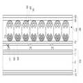
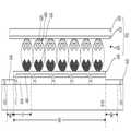
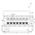
도시한 바와 같이, 종래의 전기영동 표시장치(1)는 제 1 및 제 2 기판(11, 36)과, 상기 제 1 및 제 2 기판(11, 36) 사이에 개재된 잉크층(57)을 포함한다. 상기 잉크층(57)은 축중합 반응을 통해 하전된 다수의 화이트 안료(59)와 블랙 안료(61)가 채워진 다수의 캡슐(63)을 포함한다.As shown in the drawing, the conventional
한편, 상기 제 1 기판(11)에는 다수의 박막트랜지스터(미도시)에 연결된 다수의 화소전극(28)이 화소영역(미도시) 별로 형성되고 있다. 즉, 상기 다수의 화소전극(28)은 선택적으로 (+)전압 또는 (-)전압을 각각 인가받는다. 이때, 상기 화이트 안료(59)와 블랙 안료(61)를 포함한 캡슐(63)의 크기가 일정하지 않을 경우, 선택적으로 일정 크기의 캡슐(63) 만을 선별하여 사용할 수 있다.Meanwhile, a plurality of
전술한 잉크층(57)에 (+) 극성 또는 (-) 극성을 띄는 전압을 인가하게 되면, 캡슐(63) 내부의 하전된 화이트 안료 및 블랙 안료(59, 61)는 반대 극성 쪽으로 끌려가게 된다. 즉, 상기 블랙 안료(61)가 상측으로 이동하면 블랙을 표시하게 되고, 상기 화이트 안료(59)가 상측으로 이동하게 되면 화이트를 표시하게 되는 원리를 이용한 것이다.Applying a voltage of positive or negative polarity to the
이하, 첨부한 도면을 참조하여 종래에 따른 전기영동 표시장치에 대해 보다 상세히 설명하도록 한다.Hereinafter, an electrophoretic display device according to the related art will be described in detail with reference to the accompanying drawings.
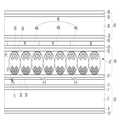
도 2는 종래에 따른 전기영동 표시장치를 개략적으로 나타낸 단면도로, 도 1과 동일한 명칭에 대해서는 동일한 도면 번호를 사용하도록 한다.FIG. 2 is a schematic cross-sectional view of a conventional electrophoretic display device, and the same reference numerals are used for the same names as those of FIG. 1.
도시한 바와 같이, 종래에 따른 전기영동 표시장치(1)는 대향 합착된 제 1 및 제 2 기판(11, 36)과, 상기 제 1 및 제 2 기판(11, 36) 사이에 개재된 잉크층(57)을 포함한다. 상기 잉크층(57)은 마주보는 면에 대응하여 투명한 물질로 이루어진 제 1 및 제 2 접착층(51, 53)과, 그 사이에 투명 도전성 물질로 이루어진 공통전극(55)과, 축중합 반응을 통해 하전된 다수의 블랙 안료(61)와 화이트 안료(59)가 채워진 다수의 캡슐(63)과 더불어 필름 형태로써 부착된다. 또한, 상기 블랙 안료(82)는 (+)극성, 화이트 안료(84)는 (-)극성으로 각각 하전된다.As shown in the drawing, the
상기 제 2 기판(36)은 투명한 플라스틱 재질이나 유리가 이용되고, 상기 제 1 기판(11)은 불투명한 스테인레스(stainless) 재질이 주로 이용되며, 필요에 따라서는 투명한 플라스틱 재질이나 투명한 유리 재질이 이용될 수 있다.The
이때, 상기 제 2 기판(36)의 하부 전면에는 적, 녹, 청색의 컬러필터 패턴으로 구성된 컬러필터층(40)이 형성되고 있다.In this case, a
한편, 상기 제 1 기판(10)에는 매트릭스 형태로 수직 교차하여 화소영역(P)을 정의하는 게이트 배선(미도시)과 데이터 배선(미도시)이 구성되고, 상기 게이트 배선(미도시)과 데이터 배선(미도시)의 교차지점에는 화소영역(P)별로 스위칭 소자 인 박막트랜지스터(Tr)가 구성된다.On the other hand, a gate wiring (not shown) and a data wiring (not shown) are formed on the first substrate 10 to vertically intersect in a matrix to define the pixel region P. The gate wiring (not shown) and data are formed on the first substrate 10. The thin film transistor Tr, which is a switching element, is formed for each pixel region P at an intersection point of the wiring (not shown).
상기 박막트랜지스터(Tr)는 게이트 배선(미도시)에서 연장된 게이트 전극(14)과, 상기 게이트 전극(14)을 덮는 게이트 절연막(16)과, 상기 게이트 전극(14)과 중첩하며 액티브층(18a)과 오믹콘택층(18b)으로 구성된 반도체층(18)과, 상기 반도체층(18)과 접촉하고 데이터 배선(미도시)에서 연장된 소스 전극(20)과, 상기 소스 전극(20)과 이격된 드레인 전극(22)을 포함한다.The thin film transistor Tr overlaps the
또한, 상기 박막트랜지스터(Tr)의 상부에는 상기 드레인 전극(22)을 노출하는 드레인 콘택홀(27)을 포함하는 보호층(26)이 전면에 구성된다.In addition, a
상기 보호층(26) 상에는 드레인 콘택홀(27)을 통해 드레인 전극(22)과 연결된 화소전극(28)이 각 화소영역(P)에 대응하여 구성되고 있다. 상기 화소전극(28)은 주로 투명 도전성 물질 예를들면 인듐-틴-옥사이드(ITO)와 인듐-징크-옥사이드(IZO)중 선택된 하나로 구성된다.The
전술한 구성을 갖는 전기영동 표시장치(1)는 자연광이나 실내광을 포함하는 외부광을 광원으로 이용하고, 박막트랜지스터(Tr)에 의해 (+)극성 또는 (-)극성을 선택적으로 인가받는 화소전극(28)이 캡슐(63) 내부에 채워진 다수의 화이트 안료(59)와 블랙 안료(61)의 위치 변화를 유도하여 영상을 구현하게 된다.The
이후에는 전술한 구성을 갖는 전기영동 표시장치의 제조 방법에 대해 설명한다.Hereinafter, a method of manufacturing the electrophoretic display device having the above-described configuration will be described.
도 3a 내지 도 3e는 종래의 전기영동 표시장치의 제조 방법에 따른 제조 단계별 공정 단면도이다. 이때 설명의 편의를 위해 다수의 화소영역(P)이 형성된 영 역을 표시영역, 상기 표시영역 외측을 비표시영역이라 정의한다.3A to 3E are cross-sectional views illustrating manufacturing steps according to a manufacturing method of a conventional electrophoretic display device. In this case, for convenience of description, an area in which a plurality of pixel areas P is formed is defined as a display area, and an outside of the display area is defined as a non-display area.
우선, 도 3a에 도시한 바와 같이, 제 1 캐리어 기판(5) 예를들면 유리기판의 상면 및 하면에 각각 제 1 및 제 2 접착층(7, 9)을 형성하고, 상기 제 1 및 제 2 접착층(7, 9) 외측으로 각각 스테인레스 재질의 제 1 및 제 2 금속박막 기판(11, 13)을 부착한다.First, as shown in FIG. 3A, first and second
다음, 상기 제 1 금속박막 기판(11) 위로 전면에 절연층(미도시)을 형성하고, 상기 절연층(미도시) 위로 서로 교차하여 화소영역(P)을 정의하는 게이트 및 데이터 배선(미도시)을 형성하고, 상기 각 화소영역(P)에 상기 게이트 배선(미도시) 및 데이터 배선(미도시)과 연결되는 박막트랜지스터(Tr)를 형성한다. 이때 다수의 화소영역(P)으로 구성되는 표시영역(미도시) 외측의 비표시영역(미도시)에는 상기 게이트 배선(미도시)과 연결되며 게이트 패드전극(미도시)이, 상기 데이터 배선(미도시)과 연결되며 데이터 패드전극(미도시)이 형성된다.Next, an insulating layer (not shown) is formed on the entire surface of the first metal
이후, 상기 박막트랜지스터(Tr) 위로 전면에 유기절연물질을 도포하여 보호층(26)을 형성하고 이를 패터닝하여 각 화소영역(P)에 있어 상기 박막트랜지스터(Tr)의 드레인 전극(미도시)을 노출시키는 드레인 콘택홀(27)과 상기 게이트 및 데이터 패드전극(미도시)을 각각 노출시키는 게이트 및 데이터 패드 콘택홀(미도시)을 형성한다.Subsequently, an organic insulating material is coated on the entire surface of the thin film transistor Tr to form a
다음, 상기 보호층(26) 위로 투명 도전성 물질을 증착하고 패터닝함으로써 각 화소영역(P) 별로 상기 드레인 콘택홀(27)을 통해 상기 드레인 전극(미도시)과 접촉하는 화소전극(28)을 형성하고, 상기 비표시영역(미도시)에 있어서는 각 게이트 및 데이터 패드전극(미도시)과 접촉하는 게이트 및 데이터 보조 패드전극(미도시)을 형성함으로써 전기영동 표시장치용 어레이 기판(22)을 완성한다.Next, a
다음, 도 3b에 도시한 바와 같이, 제 2 캐리어 기판(30) 예를들면 유리기판의 상면 및 하면에 각각 제 3 및 제 4 접착층(32, 34)을 형성하고, 상기 각 접착층(32, 34)의 외측으로 유연한 특성을 갖는 플라스틱 재질의 제 1 및 2 투명기판(36, 38)을 부착한다.3B, the third and fourth
이후, 상기 제 1 투명기판(36) 상부로 상기 어레이 기판(22)의 각 화소영역(P)에 대응하여 적, 녹, 청색의 컬러필터 패턴(40a, 40b, 40c)이 순차 반복되는 형태의 컬러필터층(40)을 형성함으로써 전기영동 표시장치용 컬러필터 기판(42)을 완성한다. 이때, 상기 각 컬러필터 패턴(40a, 40b, 40c)의 테두리와 중첩하며 상기 각 화소영역(P)을 테두리하며 블랙매트릭스(미도시)를 더욱 형성할 수도 있다.Subsequently, red, green, and blue
다음, 도 3c에 도시한 바와 같이, 상기 전기영동 표시장치용 어레이 기판(22)에 최외각에 제 5 및 제 6 접착층(51, 53)을 가지며 그 사이에 축중합 반응을 통해 하전된 다수의 화이트 안료(59)와 블랙 안료(61)가 채워진 다수의 캡슐(63)을 포함하는 잉크층(57)과 투명 도전성 물질로 전면에 공통전극(55)이 형성된 것을 특징으로 하는 전기영동 필름(65)을 부착한다. 이때 상기 공통전극(55)이 잉크층(57) 상부에 위치하도록 부착하는 것이 특징이다.Next, as illustrated in FIG. 3C, a plurality of fifth and sixth
다음 도 3d에 도시한 바와 같이, 상기 전기영동 필름(65)이 부착된 어레이 기판(22)에 대향하여 상기 전기영동 표시장치용 컬러필터 기판(42)을 상기 컬러필 터층(40)과 상기 전기영동 필름(65)이 마주하도록 대향시킨 후, 합착함으로써 패널 상태를 이루도록 한다.Next, as shown in FIG. 3D, the
다음, 도 3e에 도시한 바와 같이, 상기 패널 상태를 이룬 상태에서 상기 어레이 기판(도 3d의 22)을 이루는 구성요소 중 제 1 캐리어기판(5)과 그 외측의 제 1 및 제 2 접착층(7, 9)과 제 2 금속박막 기판(13)을 탈착하고, 연속하여 컬러필터 기판(도 3d의 65)에 있어서는 제 2 캐리어기판(30)과 그 양면의 제 3 및 제 4 접착층(32, 34)과 제 2 투명기판(38)을 탈착함으로써 전기영동 표시장치(1)를 완성한다.Next, as shown in FIG. 3E, the
하지만, 전술한 종래의 전기영동 표시장치의 제조 방법은 어레이 기판의 경우 제 1 캐리어기판 양면에 제 1 및 제 2 접착층을 개재한 후 스테인레스 재질의 제 1 및 제 2 금속박막 기판을 점착한 상태에서 상기 제 1 금속박막 기판 상에 박막트랜지스터를 형성하고, 컬러필터 기판의 경우 제 2 캐리어기판 양면에 유연한 플라스틱 재질의 제 1 및 제 2 투명기판을 제 3 및 제 4 접착층을 개재하여 점착하고 상기 제 1 투명기판 상에 컬러필터층을 형성하는 등의 과정을 거치며, 나아가 상기 어레이 기판과 컬러필터 기판을 합착한 후, 제 1 및 2 캐리어기판을 포함하여 불필요한 부분을 다시 탈착시키는 공정을 진행하고 있으므로 제조 과정이 복잡한 문제가 발생하고 있다.However, in the above-described method of manufacturing an electrophoretic display device, in the case of an array substrate, the first and second metal thin film substrates of stainless material are attached to each other after interposing the first and second adhesive layers on both sides of the first carrier substrate. A thin film transistor is formed on the first metal thin film substrate, and in the case of a color filter substrate, the first and second transparent substrates made of a flexible plastic material are adhered to both sides of the second carrier substrate through the third and fourth adhesive layers, 1 through the process of forming a color filter layer on the transparent substrate, and furthermore, after bonding the array substrate and the color filter substrate, the process of removing the unnecessary parts including the first and second carrier substrate again The process is complicated.
또한, 전기영동 표시장치의 제조 과정에서는 필요하지만, 최종적인 상태에서는 불필요한 구성요소의 탈착 공정 진행에 의해 스트레스에 의한 밀림 등이 발생하여 상기 어레이 기판과 컬러필터 기판의 정렬오차가 심하게 발생함으로써 표시품질 을 저하시키는 문제가 발생하고 있다.In addition, in the manufacturing process of the electrophoretic display device, in the final state, the desorption process of the unnecessary components occurs due to the progress of the desorption process of the components, resulting in severe alignment errors between the array substrate and the color filter substrate. There is a problem of lowering.
또한, 최종적으로 전기영동 표시장치의 컬러필터 기판을 이루는 비교적 경도가 낮은 플라스틱 재질의 제 1 투명기판의 경우 그 부착과 탈착 과정에서 스크레치가 다수 발생하는 문제가 있다.In addition, there is a problem that a large number of scratches are generated in the process of attaching and detaching the first transparent substrate having a relatively low hardness of plastic, which finally forms the color filter substrate of the electrophoretic display.
본 발명은 전술한 문제를 해결하기 위해 안출된 것으로, 제조 방법을 단순화 하며, 탈부착에 의한 상하 기판간 오차 발생 및 스트레치 발생을 최소화할 수 있는 전기영동 표시장치 및 그 제조 방법을 제공하는 것을 목적으로 한다.Disclosure of Invention The present invention has been made to solve the above-described problem, and an object thereof is to provide an electrophoretic display device and a method of manufacturing the same, which simplifies the manufacturing method and minimizes the occurrence of errors and stretches between upper and lower substrates due to detachment. do.
전술한 목적을 달성하기 위하여, 본 발명은 화소영역을 포함하는 표시영역과, 상기 표시영역 주변의 비표시영역이 정의된 기판 상에 형성된 스위칭 소자와; 상기 스위칭 소자를 덮는 보호층과; 상기 보호층 상에 형성되며 상기 스위칭 소자에 연결된 화소전극과; 상기 화소전극 상부에 위치하며, 다수의 하전 입자를 포함하는 잉크층과 PET로 이루어지는 베이스 필름을 포함하는 전기영동 필름과; 상기 화소전극과 전계를 형성하여 상기 전기영동 필름을 구동하는 공통전극과; 100℃이하의 공정온도에서 상기 전기영동 필름 상에 직접 형성되는 컬러필터층을 포함하는 전기영동 표시장치를 제공한다.In order to achieve the above object, the present invention provides a display device including a display area including a pixel area and a switching element formed on a substrate on which a non-display area around the display area is defined; A protective layer covering the switching element; A pixel electrode formed on the protective layer and connected to the switching element; An electrophoretic film positioned on the pixel electrode and including an ink layer including a plurality of charged particles and a base film made of PET; A common electrode configured to form an electric field with the pixel electrode to drive the electrophoretic film; It provides an electrophoretic display device including a color filter layer formed directly on the electrophoretic film at a process temperature of less than 100 ℃.
상기 컬러필터층은 적, 녹, 청색 컬러필터 패턴을 포함하며, 상기 적, 녹, 청색 컬러필터 패턴은 20~40 wt%의 에폭시와 60~80wt%의 아크릴계 바인더로 이루어지는 레지스트에 각각 적, 녹, 청색 안료가 첨가된 것이 특징이다.The color filter layer may include red, green, and blue color filter patterns, and the red, green, and blue color filter patterns may be red, green, or blue, respectively, in resists composed of 20-40 wt% epoxy and 60-80 wt% acrylic binder. It is characterized by the addition of blue pigments.
상기 화소전극의 길이와 폭은 상기 화소영역의 길이와 폭보다 각각 작고, 상기 적, 녹, 청색 컬러필터 패턴 각각의 길이는 상기 화소영역의 길이와 동일하며, 상기 적, 녹, 청색 컬러필터 패턴 각각의 폭은 상기 화소전극의 폭과 같거나 작고, 상기 적, 녹, 청색 컬러필터 패턴은 상기 폭 방향을 따라 교대로 배열되는 것이 특징이다.The length and width of the pixel electrode are smaller than the length and width of the pixel area, respectively, and the length of each of the red, green, and blue color filter patterns is the same as the length of the pixel area, and the red, green, and blue color filter patterns Each width is equal to or smaller than the width of the pixel electrode, and the red, green, and blue color filter patterns are alternately arranged along the width direction.
상기 컬러필터층은 화이트 컬러필터 패턴을 포함하며, 상기 화이트 컬러필터 패턴은 포토아크릴 또는 벤조사이클로 부텐으로 이루어지는 것이 특징이다.The color filter layer includes a white color filter pattern, and the white color filter pattern is made of photoacryl or benzocyclobutene.
상기 화소전극의 길이와 폭은 상기 화소영역의 길이와 폭보다 각각 작고, 상기 적, 녹, 청, 백색 컬러필터 패턴 각각의 길이와 폭은 상기 화소전극의 길이와 폭과 같거나 작으며, 상기 적, 녹, 청, 백색 컬러필터 패턴은 매트릭스 형태로 배열되는 것이 특징이다.The length and width of the pixel electrode are smaller than the length and width of the pixel area, respectively, and the length and width of each of the red, green, blue, and white color filter patterns are equal to or smaller than the length and width of the pixel electrode. The red, green, blue, and white color filter patterns are arranged in a matrix.
상기 보호층은 상기 표시영역에 대응하여 제 1 두께를 갖고, 상기 비표시영역에 대응하여 상기 제 1 두께보다 작은 제 2 두께를 갖는 것이 특징이다.The protective layer has a first thickness corresponding to the display area and a second thickness smaller than the first thickness corresponding to the non-display area.
상기 보호층은 상기 스위칭 소자의 일부를 노출시키는 콘택홀을 포함하고, 상기 화소전극은 상기 콘택홀을 통해 상기 스위칭 소자와 연결되며, 상기 화소전극은 상기 보호층 상에서 상기 스위칭 소자를 완전히 덮는 것을 특징으로 한다.The protective layer includes a contact hole exposing a portion of the switching element, the pixel electrode is connected to the switching element through the contact hole, the pixel electrode completely covers the switching element on the protective layer. It is done.
상기 보호층은 유기절연물질로 이루어지며, 상기 제 1 두께는 2.5㎛이상인 것을 특징으로 한다.The protective layer is made of an organic insulating material, the first thickness is characterized in that more than 2.5㎛.
상기 화소전극은 불투명한 금속물질인 몰리-티타늄(MoTi)으로 이루어지는 것이 특징이다.The pixel electrode may be formed of molten titanium (MoTi), which is an opaque metal material.
상기 보호층과 상기 화소전극 사이에 위치하며, 상기 스위칭 소자를 덮고 불투명한 금속물질인 몰리브덴으로 이루어지는 차광패턴을 포함하는 것이 특징이다.The light blocking pattern may be disposed between the passivation layer and the pixel electrode to cover the switching device and include a light blocking pattern made of molybdenum, an opaque metal material.
상기 보호층은, 상기 표시영역에 있어서는 순차 적층된 무기절연물질층과 제 3 두께의 제 1 유기절연물질층의 이중층 구조를 가지며, 상기 비표시영역에 있어서는 상기 무기절연물질층의 단일층 구조 또는 상기 무기절연물질층과 상기 제 3 두께보다 작은 제 4 두께를 갖는 제 2 유기절연물질층의 이중층 구조를 갖는 것이 특징이다.The protective layer has a double layer structure of an inorganic insulating material layer sequentially stacked in the display area and a first organic insulating material layer having a third thickness, and in the non-display area, a single layer structure of the inorganic insulating material layer or And a double layer structure of the inorganic insulating material layer and the second organic insulating material layer having a fourth thickness smaller than the third thickness.
상기 보호층은, 상기 표시영역에 있어서는 순차 적층된 제 3 두께의 제 1 유기절연물질층과 무기절연물질층의 이중층 구조를 가지며, 상기 비표시영역에 있어서는 상기 제 3 두께보다 작은 제 4 두께를 갖는 제 2 유기절연물질층의 단일층 구조를 갖는 것이 특징이다.The protective layer has a double layer structure of a first organic insulating material layer and an inorganic insulating material layer having a third thickness that are sequentially stacked in the display area, and a fourth thickness smaller than the third thickness in the non-display area. It is characterized by having a single layer structure of the second organic insulating material layer having.
상기 보호층은, 상기 표시영역에 있어서는 제 1 무기절연물질층과, 제 3 두께의 제 1 유기절연물질층과, 제 2 무기절열물질층의 삼중층 구조를 가지며, 상기 비표시영역에 있어서는, 상기 제 1 무기절연물질층과, 상기 제 3 두께보다 작은 제 4 두께를 갖는 제 2 유기절연물질층의 이중층 구조를 갖는 것이 특징이다.The protective layer has a triple layer structure of a first inorganic insulating material layer, a first organic insulating material layer having a third thickness, and a second inorganic insulating material layer in the display area, and in the non-display area, And a double layer structure of the first inorganic insulating material layer and the second organic insulating material layer having a fourth thickness smaller than the third thickness.
상기 보호층은, 상기 표시영역에 있어서는 제 1 무기절연물질층과, 유기절연물질층과, 제 2 무기절열물질층의 삼중층 구조를 가지며, 상기 비표시영역에 있어 서는, 상기 제 1 무기절연물질층의 단일층 구조를 갖는 것이 특징이다.The protective layer has a triple layer structure of a first inorganic insulating material layer, an organic insulating material layer, and a second inorganic insulating material layer in the display area, and in the non-display area, the first inorganic insulating material. It is characterized by having a single layer structure of the material layer.
상기 컬러필터층은 포토리소그라피 공정을 통해 형성되거나, 잉크젯 장치 또는 롤 프린팅 장치에 의해 형성되는 것이 특징이다.The color filter layer is formed through a photolithography process, or is formed by an inkjet device or a roll printing device.
상기 베이스 필름의 두께는 30㎛보다 작은 것이 특징이다.The thickness of the base film is characterized in that less than 30㎛.
상기 공통전극은 상기 잉크층과 상기 베이스 필름 사이에 위치하는 것이 특징이다.The common electrode is positioned between the ink layer and the base film.
상기 표시영역에 형성되며 상기 스위치 소자의 제 1 전극과 연결되고 제 1 방향으로 연장된 게이트 배선과; 상기 표시영역에 형성되며 상기 스위칭 소자의 제 2 전극과 연결되고 상기 제 1 방향과 다른 제 2 방향으로 연장된 데이터 배선과; 상기 비표시영역에 형성되며 상기 게이트 배선의 일끝에 연결되는 게이트 패드 전극과; 상기 비표시영역에 형성되며 상기 데이터 배선의 일끝에 연결되는 데이터 패드 전극을 포함하며, 상기 보호층은 상기 게이트 패드 전극을 노출시키는 게이트 패드 콘택홀과, 상기 데이터 패드 전극을 노출시키는 데이터 패드 콘택홀을 포함하는 것이 특징이다.A gate line formed in the display area and connected to a first electrode of the switch element and extending in a first direction; A data line formed in the display area and connected to a second electrode of the switching element and extending in a second direction different from the first direction; A gate pad electrode formed in the non-display area and connected to one end of the gate line; And a data pad electrode formed in the non-display area and connected to one end of the data line, wherein the protective layer includes a gate pad contact hole exposing the gate pad electrode and a data pad contact hole exposing the data pad electrode. It is characterized by including.
상기 전기영동 필름은 상기 화소전극과 접촉하는 접착층을 포함하며, 상기 잉크층은 상기 베이스 필름과 상기 접착층 사이에 위치하는 것을 특징으로 한다.The electrophoretic film includes an adhesive layer in contact with the pixel electrode, and the ink layer is positioned between the base film and the adhesive layer.
상기 잉크층은 축중합 반응을 통해 하전된 다수의 화이트 안료와 블랙 안료가 채워진 다수의 캡슐로 이루어진 것이 특징이다.The ink layer is characterized by consisting of a plurality of capsules filled with a plurality of white pigments and black pigment charged through a polycondensation reaction.
상기 컬러필터층을 덮는 보호시트를 포함하는 것이 특징이다.It characterized in that it comprises a protective sheet covering the color filter layer.
다른 관점에서, 본 발명은 화소영역을 포함하는 표시영역과, 상기 표시영역 주변의 비표시영역이 정의된 기판 상에 스위칭 소자를 형성하는 단계와; 상기 스위칭 소자를 덮는 보호층을 형성하는 단계와; 상기 보호층 상에 형성되며 상기 스위칭 소자에 연결된 화소전극을 형성하는 단계와; 상기 화소전극 상부에, 다수의 하전 입자를 포함하는 잉크층과, 상기 화소전극과 전계를 형성하는 공통전극과, PET로 이루어지는 베이스 필름을 포함하는 전기영동 필름을 부착하는 단계와; 100℃이하의 공정온도에서 상기 전기영동 필름 상에 직접 컬러필터층을 형성하는 단계를 포함하는 전기영동 표시장치의 제조방법을 제공한다.In another aspect, the present invention provides a method for manufacturing a display device including: forming a switching element on a display area including a pixel area and a non-display area around the display area; Forming a protective layer covering the switching element; Forming a pixel electrode formed on the protective layer and connected to the switching element; Attaching an electrophoretic film including an ink layer including a plurality of charged particles, a common electrode forming an electric field with the pixel electrode, and a base film made of PET on the pixel electrode; It provides a method of manufacturing an electrophoretic display device comprising forming a color filter layer directly on the electrophoretic film at a process temperature of less than 100 ℃.
상기 컬러필터층은 적, 녹, 청색 컬러필터 패턴을 포함하며, 상기 적, 녹, 청색 컬러필터 패턴은 20~40 wt%의 에폭시와 60~80wt%의 아크릴계 바인더로 이루어지는 레지스트에 각각 적, 녹, 청색 안료가 첨가된 것이 특징이다.The color filter layer may include red, green, and blue color filter patterns, and the red, green, and blue color filter patterns may be red, green, or blue, respectively, in resists composed of 20-40 wt% epoxy and 60-80 wt% acrylic binder. It is characterized by the addition of blue pigments.
상기 화소전극의 길이와 폭은 상기 화소영역의 길이와 폭보다 각각 작고, 상기 적, 녹, 청색 컬러필터 패턴 각각의 길이는 상기 화소영역의 길이와 동일하며, 상기 적, 녹, 청색 컬러필터 패턴 각각의 폭은 상기 화소전극의 폭과 같거나 작고, 상기 적, 녹, 청색 컬러필터 패턴은 상기 폭 방향을 따라 교대로 배열되는 것이 특징이다.The length and width of the pixel electrode are smaller than the length and width of the pixel area, respectively, and the length of each of the red, green, and blue color filter patterns is the same as the length of the pixel area, and the red, green, and blue color filter patterns Each width is equal to or smaller than the width of the pixel electrode, and the red, green, and blue color filter patterns are alternately arranged along the width direction.
상기 컬러필터층은 화이트 컬러필터 패턴을 포함하며, 상기 화이트 컬러필터 패턴은 포토아크릴 또는 벤조사이클로 부텐으로 이루어지는 것이 특징이다.The color filter layer includes a white color filter pattern, and the white color filter pattern is made of photoacryl or benzocyclobutene.
상기 화소전극의 길이와 폭은 상기 화소영역의 길이와 폭보다 각각 작고, 상기 적, 녹, 청, 백색 컬러필터 패턴 각각의 길이와 폭은 상기 화소전극의 길이와 폭과 같거나 작으며, 상기 적, 녹, 청, 백색 컬러필터 패턴은 매트릭스 형태로 배열되는 것이 특징이다.The length and width of the pixel electrode are smaller than the length and width of the pixel area, respectively, and the length and width of each of the red, green, blue, and white color filter patterns are equal to or smaller than the length and width of the pixel electrode. The red, green, blue, and white color filter patterns are arranged in a matrix.
상기 스위칭 소자의 형성 단계는, 상기 기판 상에 게이트 배선을 형성하는 단계와; 상기 게이트 배선을 덮는 게이트 절연막을 형성하는 단계와; 상기 게이트 절연막 상에 상기 게이트 배선과 교차하는 데이터 배선을 형성하는 단계를 포함하며, 상기 게이트 배선의 형성단계, 상기 데이터 배선의 형성 단계 또는 상기 화소전극의 형성 단계 중 어느 하나는 상기 비표시영역에 얼라인 마크를 형성하는 단계를 더욱 포함하며, 상기 컬러필터층은 상기 얼라인 마크를 이용하여 얼라인하여 형성되는 것이 특징이다.The forming of the switching element may include forming a gate wiring on the substrate; Forming a gate insulating film covering the gate wiring; And forming a data line intersecting the gate line on the gate insulating layer, wherein any one of forming the gate line, forming the data line, or forming the pixel electrode is formed in the non-display area. The method may further include forming an alignment mark, wherein the color filter layer is formed by aligning the alignment mark.
상기 얼라인 마크는 상기 표시영역 주변의 서로 다른 3개 영역에 각각 1개씩 형성되는 것이 특징이다.Each of the alignment marks is formed in three different regions around the display area.
상기 화소전극의 형성단계는, 몰리-티타늄(MoTi)으로 이루어지는 불투명 금속층을 형성하는 단계와, 상기 불투명한 금속층을 패턴하여 상기 화소전극 및 상기 비표시영역에 얼라인 마크를 형성하는 단계를 포함하며, 상기 화소전극은 상기 스위칭 소자를 완전히 덮고, 상기 컬러필터층은 상기 얼라인 마크를 이용하여 얼라인하여 형성되는 것이 특징이다.The forming of the pixel electrode may include forming an opaque metal layer formed of molybdenum (MoTi), and forming an alignment mark on the pixel electrode and the non-display area by patterning the opaque metal layer. The pixel electrode completely covers the switching element, and the color filter layer is formed by aligning the alignment mark.
상기 화소영역의 형성 단계 전에, 상기 보호층 상에 불투명한 금속층을 형성하는 단계와; 상기 불투명한 금속층을 패턴하여 상기 박막트랜지스터를 덮는 차광패턴과 상기 비표시영역에 얼라인 마크를 형성하는 단계를 포함하며, 상기 컬러필터층은 상기 얼라인 마크를 이용하여 얼라인하여 형성되는 것이 특징이다.Before forming the pixel region, forming an opaque metal layer on the protective layer; And forming an alignment mark on the light blocking pattern covering the thin film transistor and the non-display area by patterning the opaque metal layer, wherein the color filter layer is aligned by using the alignment mark.
상기 컬러필터층은 포토리소그라피 공정을 통해 형성되거나, 잉크젯 장치 또는 롤 프린팅 장치에 의해 형성되는 것이 특징이다.The color filter layer is formed through a photolithography process, or is formed by an inkjet device or a roll printing device.
상기 베이스 필름의 두께는 30㎛보다 작은 것이 특징이다.The thickness of the base film is characterized in that less than 30㎛.
상기 보호층은 상기 표시영역에 대응하여 제 1 두께를 갖고, 상기 비표시영역에 대응하여 상기 제 1 두께보다 작은 제 2 두께를 갖는 것이 특징이다.The protective layer has a first thickness corresponding to the display area and a second thickness smaller than the first thickness corresponding to the non-display area.
상기 보호층은 상기 스위칭 소자의 일부를 노출시키는 콘택홀을 포함하고, 상기 화소전극은 상기 콘택홀을 통해 상기 스위칭 소자와 연결되며, 상기 화소전극은 상기 보호층 상에서 상기 스위칭 소자를 완전히 덮는 것을 특징으로 한다.The protective layer includes a contact hole exposing a portion of the switching element, the pixel electrode is connected to the switching element through the contact hole, the pixel electrode completely covers the switching element on the protective layer. It is done.
상기 보호층은 유기절연물질로 이루어지며, 상기 제 1 두께는 2.5㎛이상인 것을 특징으로 한다.The protective layer is made of an organic insulating material, the first thickness is characterized in that more than 2.5㎛.
또 다른 관점에서, 본 발명은 표시영역과, 상기 표시영역 주변의 비표시영역이 정의되어 있는 기판과; 상기 기판 상에 서로 교차하는 게이트 배선 및 데이터 배선과; 상기 게이트 배선과 연결된 게이트 전극과, 상기 게이트 전극을 덮는 게이트 절연막과, 상기 게이트 절연막 상의 반도체층과, 상기 반도체층 상에 위치하며 상기 데이터 배선과 연결된 소스 전극과, 상기 반도체층 상에서 상기 소스 전극과 이격하여 위치하는 드레인 전극을 포함하는 박막트랜지스터와; 상기 박막트랜지스터를 포함하여 상기 기판 전체를 덮으며, 상기 표시영역에 대응하여 제 1 무기절연물질층, 유기절연물질층, 제 2 무기절연물질층의 삼중층 구조를 갖고, 상기 비표시영역에 대응하여 상기 제 1 무기절연물질층의 단일층 구조를 가지며, 상기 드레인 전극을 노출시키는 드레인 콘택홀을 포함하는 보호층과; 상기 보호층 상에 위치하여, 상기 드레인 콘택홀을 통해 상기 드레인 전극과 연결되며, 상기 박막트랜지스터 전체를 덮는 화소전극과; 상기 화소전극 상에 위치하며, 접착층과, 상기 접착층 상에 위치하며 다수의 하전된 입자로 이루어지는 잉크층과, 상기 잉크층 상의 공통전극과, 상기 공통전극 상에 위치하며 PET로 이루어지는 베이스 필름을 포함하는 전기영동 필름과; 상기 전기영동 필름 상에 직접 형성되는 컬러필터층과; 상기 컬러필터층 상에 위치하는 보호시트를 포함하는 전기영동 표시장치를 제공한다.In still another aspect, the present invention provides a display device comprising: a display area and a substrate on which a non-display area around the display area is defined; Gate wiring and data wiring crossing each other on the substrate; A gate electrode connected to the gate wiring, a gate insulating film covering the gate electrode, a semiconductor layer on the gate insulating film, a source electrode on the semiconductor layer and connected to the data wiring, and a source electrode on the semiconductor layer; A thin film transistor including a drain electrode spaced apart from each other; Including the thin film transistor, the entire substrate is covered, and has a triple layer structure of a first inorganic insulating material layer, an organic insulating material layer, and a second inorganic insulating material layer corresponding to the display area, and corresponds to the non-display area. A protective layer having a single layer structure of the first inorganic insulating material layer and including a drain contact hole exposing the drain electrode; A pixel electrode on the passivation layer, connected to the drain electrode through the drain contact hole, and covering the entire thin film transistor; Located on the pixel electrode, an adhesive layer, an ink layer on the adhesive layer and consisting of a plurality of charged particles, a common electrode on the ink layer, and a base film on the common electrode made of PET An electrophoretic film; A color filter layer directly formed on the electrophoretic film; The present invention provides an electrophoretic display device including a protective sheet on the color filter layer.
상기 베이스 필름은 30㎛이하의 두께를 갖는 것이 특징이다.The base film is characterized by having a thickness of less than 30㎛.
상기 컬러필터층은 포토리소 그라피 공정을 통해 형성되거나, 잉크젯 장치 또는 롤 프린팅 장치를 이용하여 형성되는 것이 특징이다.The color filter layer may be formed through a photolithography process or may be formed using an inkjet device or a roll printing device.
상기 적, 녹, 청색 컬러필터 패턴을 포함하며, 상기 적, 녹, 청색 컬러필터 패턴은 20~40 wt%의 에폭시와 60~80wt%의 아크릴계 바인더로 이루어지는 레지스트에 각각 적, 녹, 청색 안료가 첨가된 것이며, 100℃이하의 공정 온도에서 형성되는 것이 특징이다.The red, green, and blue color filter patterns include red, green, and blue color filter patterns, wherein red, green, and blue pigments are respectively added to resists composed of 20 to 40 wt% epoxy and 60 to 80 wt% acrylic binder. It is added, it is characterized by being formed at a process temperature of 100 ℃ or less.
상기 유기절연물질층의 두께는 2.5㎛이상인 것을 특징으로 한다.The thickness of the organic insulating material layer is characterized in that more than 2.5㎛.
상기 보호층과 상기 화소전극 사이에 위치하며, 상기 박막트랜지스터를 덮고 불투명한 금속물질인 몰리브덴으로 이루어지는 차광패턴을 포함하는 것이 특징이다.The light blocking pattern may be disposed between the passivation layer and the pixel electrode to cover the thin film transistor and be formed of molybdenum, an opaque metal material.
본 발명에 따른 전기영동 표시장치는, 별도의 캐리어 기판 등을 필요로 하지 않으며, 캐리어 기판에 부착하기 위한 접착층 형성을 필요로 하지 않으므로 재료비를 절감하는 동시에 제조 공정을 단순화 하는 효과가 있다.The electrophoretic display device according to the present invention does not require a separate carrier substrate or the like, and does not require the formation of an adhesive layer for attaching to the carrier substrate, thereby reducing the material cost and simplifying the manufacturing process.
또한, 컬러필터층을 기판 상에 부착된 전기영동 필름 상에 직접 형성함으로써 컬러필터 기판을 따로 제작할 필요가 없으며, 따라서 컬러필터 기판과 어레이 소자가 구비된 기판과의 합착 시 오차 범위(통상 약 5㎛)보다 훨씬 작은 오차 범위(약 2㎛)를 갖게 되므로 합착 오차에 따른 정렬 불량을 최소화 할 수 있는 장점을 갖는다.In addition, since the color filter layer is directly formed on the electrophoretic film attached on the substrate, it is not necessary to separately manufacture the color filter substrate, and thus an error range when bonding the color filter substrate and the substrate with the array element (typically about 5 μm) Since it has a much smaller error range (about 2㎛), it has the advantage of minimizing misalignment due to the bonding error.
또한, 불필요한 구성요소(캐리어 기판 등)의 탈착 과정이 생략됨으로써 탈착 시 발생하는 스크래치 및 밀림 등에 의한 상/하판 틀어짐 등에 따른 불량을 방지하는 효과가 있다.In addition, since the detachment process of unnecessary components (carrier substrate, etc.) is omitted, it is possible to prevent defects due to the upper / lower plate warping due to scratches and slippage occurring during detachment.
또한, 보호층을 표시영역과 비표시영역에 있어 그 두께를 달리 형성함으로써 ACF를 이용한 TCP 본딩시의 쇼트 불량 또는 도전 불량을 방지할 수 있는 장점을 갖는다.In addition, since the protective layer is formed in different thicknesses in the display area and the non-display area, it is possible to prevent short or conductive defects during TCP bonding using ACF.
또한, 컬러필터층을 전기영동 필름 상에 직접 형성함에 있어, 컬러필터층의 형성 공정이 약 100℃ 이하, 바람직하게는 약 70℃이하에서 이루어지기 때문에, 전기영동 필름에 영향을 주지 않게 된다.In addition, in forming the color filter layer directly on the electrophoretic film, since the process of forming the color filter layer is performed at about 100 ° C. or less, preferably about 70 ° C. or less, the electrophoretic film is not affected.
또한, 화소전극이 박막트랜지스터를 완전히 덮도록 구성됨으로써 개구율이 향상되며, 화소전극과 박막트랜지스터 사이의 기생용량 문제는 보호층을 약 3μm이상의 두께로 형성함으로써 해결하게 된다.In addition, since the pixel electrode is configured to completely cover the thin film transistor, the aperture ratio is improved, and the parasitic capacitance problem between the pixel electrode and the thin film transistor is solved by forming a protective layer having a thickness of about 3 μm or more.
그리고, 전기영동 필름의 베이스 필름과 공통전극의 두께 합이 약 30μm이하가 되도록 함으로써, 해당 화소의 영상이 이웃한 화소를 통해 보여지는 패럴렉스 문제를 방지할 수 있다.In addition, the sum of the thicknesses of the base film and the common electrode of the electrophoretic film is about 30 μm or less, thereby preventing the parallax problem in which the image of the pixel is seen through neighboring pixels.
이하, 첨부한 도면을 참조하여 본 발명에 따른 전기영동 표시장치에 대해 설명하도록 한다. 본 발명에 따른 전기영동 표시장치는 박막트랜지스터가 구비된 어레이 기판에 필름 타입의 잉크층과 컬러필터층이 모두 형성된 것을 특징으로 한다.Hereinafter, an electrophoretic display device according to the present invention will be described with reference to the accompanying drawings. The electrophoretic display according to the present invention is characterized in that both the film type ink layer and the color filter layer are formed on the array substrate provided with the thin film transistor.
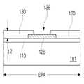
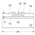
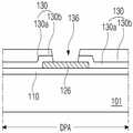
도 4a 내지 4h는 본 발명에 따른 전기영동 표시장치에 있어 박막트랜지스터가 형성되는 부분과 스토리지 커패시터가 형성되는 부분을 포함하는 하나의 화소영역에 대한의 제조 단계별 공정 단면도이며, 도 5a 내지 5h는 본 발명에 따른 전기영동 표시장치에 있어 게이트 패드부에 대한 제조 단계별 공정 단면도이며, 도 6a 내지 6h는 본 발명에 따른 전기영동 표시장치에 있어 데이터 패드부에 대한 제조 단계별 공정 단면도이다. 또한 도 7a 내지 도 7c는 본 발명에 따른 전기영동 표시장치의 제조 단계별 공정 평면도로서 표시영역과 비표시영역 및 컬러필터층 형성용 얼라인 마크의 위치를 간략히 나타낸 것이다.4A through 4H are cross-sectional views illustrating manufacturing steps of one pixel region including a portion where a thin film transistor and a storage capacitor are formed, in the electrophoretic display according to the present invention. Steps for manufacturing the gate pad part in the electrophoretic display according to the present invention are sectional views. FIGS. 6A to 6H are step views for the manufacturing step for the data pad part in the electrophoretic display according to the present invention. 7A to 7C are plan views illustrating manufacturing steps of the electrophoretic display device according to the present invention, which briefly illustrate positions of the display area, the non-display area, and the alignment mark for forming the color filter layer.
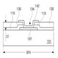
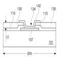
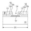
우선, 도 4a, 5a 및 도 6a에 도시한 바와 같이, 절연기판(101) 예를들면 유리기판 또는 플라스틱 기판 상에 제 1 금속물질 예를들면 알루미늄(Al), 알루미늄 합금(AlNd), 구리(Cu), 구리합금, 크롬(Cr), 티타늄 합금을 증착하여 제 1 금속층(미도시)을 형성한 후, 포토레지스트의 도포, 마스크를 이용한 노광, 포토레지스트 의 현상, 식각, 포토레지스트의 스트립(strip) 등의 공정을 포함하는 마스크 공정을 진행하여 일 방향으로 연장하는 게이트 배선(미도시)을 형성하고, 동시에 상기 스위칭 영역(TrA)에는 상기 게이트 배선(미도시)과 연결된 게이트 전극(103)을, 그리고 스토리지 영역(StgA)에는 제 1 스토리지 전극(105)을 형성한다. 이때 상기 제 1 스토리지 전극(105)은 상기 게이트 배선(미도시) 자체로 이루어지거나 또는 상기 게이트 배선(미도시)과 나란하게 공통배선(미도시)을 형성함으로써 상기 공통배선 (미도시) 일부로 이루어질 수도 있다. 또한, 게이트 패드부(GPA)에 있어서는 상기 게이트 배선(미도시)의 일끝단과 연결된 게이트 패드전극(107)을 형성한다. 이때, 상기 제 1 금속층(미도시)은 서로 다른 금속물질을 연속 증착하여 이중층 구조를 갖도록 형성할 수도 있다. 이러한 이중층 구조를 갖는 제 1 금속층을 패터닝할 경우, 예를들면 알루미늄 합금(AlNd)/몰리브덴(Mo), 티타늄 합금/구리(Cu)의 이중층 구조를 갖는 게이트 배선(미도시)과 게이트 전극(미도시), 제 1 스토리지 전극(미도시) 및 게이트 패드전극(미도시)이 되도록 형성할 수도 있다. 상기 이중층의 제 1 금속층이 몰리브덴(Mo)의 하부층과 알루미늄합금(AlNd)의 상부층으로 이루어지고, 후술하는 바와 같이 컬러필터층이 마스크 공정에 의해 전기영동 필름 상에 형성되는 경우, 상기 컬러필터층을 패턴하기 위한 현상액은 KOH의 농도가 약 0.1 wt%이하가 되도록 한다. 몰리브덴(Mo)의 단점을 보완하기 위해 알루미늄합금(AlNd)를 상부층으로 이용하는 것인데, 게이트 패드전극(107)은 컬러필터층의 마스크 공정에서 노출되며, 상부층인 알루미늄합금(AlNd)은 KOH 용액과 반응하여 녹기 때문이다. 화소전극의 형성 공정에서 게이트 패드전극(107)을 ITO로 이루어지는 게이트 보조 패드전극이 덮을 수 있지만, ITO 투명전도막의 그레인 등을 통해 현상액이 침투하여 알루미늄합금(AlNd)층에 손상을 유발시킨다. 한편, 이중층의 제 1 금속층이 티타늄 합금/구리(Cu)인 경우에는 티타늄 합금이 컬러필터층의 현상액과 반응하지 않기 때문에 위와 같은 문제는 발생하지 않는다. 도면에서는 편의상 단일층 구조를 갖는 게이트 배선(미도시)과 게이트 전극(103), 제 1 스토리지 전극(105) 및 게이트 패드전극(107)으로 나타내었다.First, as shown in FIGS. 4A, 5A, and 6A, a first metal material such as aluminum (Al), aluminum alloy (AlNd), copper (eg, on an insulating
이때, 평면도인 도 7a를 참조하면, 상기 게이트 패드부(GPA)와 데이터 패드부(DPA) 및 상기 게이트 및 데이터 패드부(GPA, DPA)가 형성되지 않은 일 비표시영역 각각의 외측영역(이 부분은 추후 절단되어 제거되는 부분임)에는 상기 제 1 금속층(미도시)을 패터닝함으로써 컬러필터층(미도시) 형성 시 필요한 얼라인 마크(191)를 형성하는 것이 특징이다. 따라서 상기 컬러필터 형성 용 얼라인 마크(191)는 게이트 및 데이터 패드부(GPA, DPA)를 포함하는 4부분의 비표시영역(NA) 외측의 절단영역 중 표시영역(DA)을 사이에 두고 서로 마주하는 양측면과 상기 양측면을 연결하는 두 부분 중 어느 하나의 부분에 각각 하나씩 모두 3개를 형성하는 것이 컬러필터층 내의 컬러필터 패턴과 각 화소영역과의 정확한 정렬을 위해 바람직하다. 이때 상기 컬러필터 형성 용 얼라인 마크(191)는 상기 게이트 배선과 게이트 전극 형성 단계에서 반드시 형성될 필요는 없으며, 이후 단계에서 형성될 수도 있다.At this time, referring to FIG. 7A, which is a plan view, an outer region of each non-display area in which the gate pad part GPA and the data pad part DPA, and the gate and data pad parts GPA and DPA are not formed is The part is a part which is later cut off and removed), thereby forming an
다음, 도 4b, 5b 및 도 6b 에 도시한 바와 같이, 상기 게이트 배선(미도시), 게이트 전극(103), 제 1 스토리지 전극(105) 및 게이트 패드전극(107) 위로 전면에 무기절연물질 예를들면 산화실리콘(SiO2) 또는 질화실리콘(SiNx)을 증착하여 게이트 절연막(110)을 형성한다. 이후 연속하여 상기 게이트 절연막(110) 위로 순수 비정질 실리콘과 불순물 비정질 실리콘을 연속하여 증착함으로써 순수 비정질 실리콘층(미도시)과 불순물 비정질 실리콘층(미도시)을 형성하고, 이를 마스크 공정을 실시함으로써 패터닝하여 상기 스위칭 영역(TrA)에 상기 게이트 전극(103)에 대응하여 액티브층(115a)과 그 상부로 불순물 비정질 실리콘 패턴(115b)을 형성한다.Next, as shown in FIGS. 4B, 5B, and 6B, an example of an inorganic insulating material is formed on the entire surface of the gate wiring (not shown), the
다음, 도 4c, 5c 및 도 6c에 도시한 바와 같이, 상기 액티브층(115a)과 불순물 비정질 실리콘패턴(도 4b의 115b)과 상기 게이트 절연막(110) 위로 제 2 금속물질 예를들면 몰리브덴(Mo), 구리(Cu), 티타늄 합금, 알루미늄 합금(AlNd) 중 어느 하나를 증착하여 전면에 제 2 금속층(미도시)을 형성한다. 이때 상기 제 2 금속층(미도시)은 상기 제 2 금속물질 중 두 가지 또는 세 가지를 연속적으로 증착하여 예를들면 티타늄 합금/구리(Cu)의 이중층 구조를 갖도록 형성하거나, 또는 몰리브덴(Mo)/알루미늄 합금(AlNd)/몰리브덴(Mo)의 3중층 구조를 갖도록 형성할 수도 있다. 도면에 있어서는 단일층 구조를 갖는 것을 일례로 도시하였다.Next, as shown in FIGS. 4C, 5C, and 6C, a second metal material such as molybdenum (Mo) is disposed on the
이후 상기 제 2 금속층(미도시)을 패터닝함으로써 상기 게이트 배선(미도시)과 교차하여 화소영역(P)을 정의하는 데이터 배선(미도시)을 형성한다. 또한 동시에 각 화소영역(P) 내의 스위칭 영역(TrA)에는 상기 불순물 비정질 실리콘패턴(도 4b의 115b) 위에서 서로 이격하는 형태로 소스 및 드레인 전극(120, 122)을 형성하며, 스토리지 영역(StgA)에는 상기 드레인 전극(122)과 연결된 제 2 스토리지 전극(124)을 형성한다. 이때 상기 소스 전극(120)은 상기 데이터 배선(미도시)과 연 결되도록 한다. 또한, 상기 데이터 패드부(DPA)에는 상기 게이트 절연막(110) 위로 상기 데이터 배선(미도시)의 일끝단과 연결되는 데이터 패드전극(126)을 형성한다. 전술한 바와 같이, 데이터 패드 전극(126)이 알루미늄합금(AlNd)의 단일층으로 이루어지거나 또는 알루미늄합금(AlNd)을 최상층으로 하여 이중층 또는 삼중층으로 이루어지는 경우에는, 알루미늄합금(AlNd)층의 손상을 방지하기 위해 컬러필터층의 패턴을 위한 현상액은 약 0.1wt%이하의 KOH를 포함하여야 한다. 그러나, 몰리브덴(Mo)의 단일층 구조, 티타늄 합금/구리(Cu)의 이중층 구조, 또는 몰리브덴(Mo)/알루미늄 합금(AlNd)/몰리브덴(Mo)의 3중층 구조를 갖는 경우에는 통상적인 현상액을 이용하여 컬러필터층의 패턴 공정을 진행하여도 무방하다.Subsequently, the second metal layer (not shown) is patterned to form a data line (not shown) that defines the pixel region P to cross the gate line (not shown). At the same time, source and drain
이후, 드라이 에칭에 의해 소스 및 드레인 전극(120, 122) 사이의 불순물 비정질 실리콘 패턴(도 4b의 115b)을 제거함으로써 상기 소스 및 드레인 전극(120, 122) 사이로 상기 액티브층(115a)이 노출되도록 하고, 상기 액티브층(115a) 상부로 각각 소스 및 드레인 전극(120, 122)과 접촉하며 서로 이격하는 불순물 비정질 실리콘의 오믹콘택층(115c)을 형성한다. 이때 상기 액티브층(115a)과 그 상부에서 서로 이격하는 오믹콘택층(115c)은 반도체층(115)을 이룬다. 상기 게이트 전극(103), 게이트 절연막(110), 상기 액티브층(115a) 및 상기 오믹콘택층(115c)으로 이루어지는 반도체층(115), 상기 소스 전극(120) 및 상기 드레인 전극(122)은 스위칭 소자인 박막트랜지스터(Tr)를 이룬다. 상기 박막트랜지스터(Tr)는 스위칭 소자로서, 상기 게이트 배선(105)에 의해 스위칭되어 화소전극에 데이터를 인가하게 된다.Thereafter, the
한편, 게이트 배선(미도시)과 게이트 전극(103)을 형성하는 단계에서 비표시 영역(도 7a의 NA)에 3개의 컬러필터층 형성 용 얼라인 마크(도 7a의 191)를 형성하지 않았을 경우, 상기 데이터 배선(미도시)과 소스 및 드레인 전극(120, 122)을 형성하는 단계에서 상기 게이트 절연막(110) 위로 전술한 비표시영역(도 7a의 NA)의 3부분에 대응하여 컬러필터층 형성용 얼라인 마크(도 7a의 191)를 형성할 수도 있다.On the other hand, in the case of forming the gate wiring (not shown) and the
한편, 전술한 반도체층(115)과 소스 및 드레인 전극(120, 122)의 형성 단계는 각각 서로 다른 2회의 마스크 공정을 통해 이루어짐을 보이고 있지만, 변형예로서 도면으로 나타내지 않았지만, 상기 게이트 절연막(110) 위로 순수 및 불순물 비정질 실리콘층을 형성하고, 이를 패터닝하기 전에 상기 불순물 비정질 실리콘층 위로 상기 제 2 금속층을 형성한 상태에서 회절노광 또는 하프톤 노광 기법을 이용한 마스크 공정을 진행함으로써 서로 다른 두께를 갖는 포토레지스트 패턴을 형성하는 것을 특징으로 하는 1회의 마스크 공정을 통해 상기 반도체층과 소스 및 드레인 전극을 형성할 수도 있다. 이 경우 상기 데이터 배선과 데이터 패드전극 하부에는 상기 반도체층을 이루는 동일한 물질로써 반도체 패턴이 형성되게 된다. 또한, 이 단계에서 컬러필터층 형성용 얼라인 마크를 형성하게 되는 경우 상기 컬러필터층 형성용 얼라인 마크 하부에도 반도체 패턴이 형성되게 된다.Meanwhile, although the above-described steps of forming the
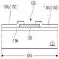
다음, 도 4d, 5d 및 도 6d에 도시한 바와 같이, 상기 데이터 배선(미도시)과 소스 및 드레인 전극(120, 122)과 제 2 스토리지 전극(124) 및 데이터 패드전극(126) 위로 전면에 유기절연물질 예를들면 포토아크릴(photo acryl) 또는 벤조사이클로부텐(BCB)을 도포하여 그 표면이 평탄한 상태를 갖는 보호층(130)을 형성한 다. 이후 상기 보호층(130)에 대해 스캔타입 노광기를 이용하여 회절노광 또는 하프톤 노광을 실시하고 이를 현상함으로써, 또는 스탭퍼 타입 노광기를 이용해서는 블랭크 샷을 포함하는 2회의 노광을 실시하고 이를 현상함으로써 화소영역(P)들로 구성된 표시영역에 대해서는 제 1 두께(t1)를 갖도록, 그리고 게이트 및 데이터 패드부(GPA, DPA)를 포함하는 비표시영역에 대응해서는 상기 제 1 두께(t1)보다 얇은 제 2 두께(t2)를 갖도록 하며, 각 화소영역(P) 내의 드레인 전극(122)과 비표시영역의 게이트 패드전극(107)과 데이터 패드전극(126)에 대응해서는 상기 드레인 전극(122)과 각각의 패드전극(107, 126)이 노출되도록 드레인 콘택홀(132)과 게이트 및 데이터 패드 콘택홀(134, 136)을 형성한다. 이때 상기 보호층(130)을 유기절연물질로 형성한 이유는 그 하부에 위치하는 화소영역(P) 내의 전극들 예를들면 제 1 및 제 2 스토리지 전극과 그 상부에 형성되는 화소전극(미도시)과 중첩됨으로써 발생하는 기생용량을 최소화하고, 그 표면이 평탄한 형태를 갖도록 하기 위함이다. 특히, 보호층(130) 상부에 형성되는 화소전극은 박막트랜지스터를 완전히 덮으며 형성되고 이러한 경우 박막트랜지스터와 화소전극 사이에 기생용량이 발생하여 표시품질을 저하시키게 된다. 따라서, 이러한 기생용량을 최소화하기 위해 상기 보호층(130)을 유기절연물질로 형성하며, 특히 그 두께를 약 2.5μm이상, 예를 들어 약 2.5~5μm로 한다. 일반적인 액정표시장치에서는 화소전극이 박막트랜지스터를 덮지 않기 때문에 그 두께가 약 1μm인 점과 비교하면, 매우 두꺼움을 알 수 있다.Next, as shown in FIGS. 4D, 5D, and 6D, the data line (not shown) and the source and drain
또한, 표시영역과 비표시영역에 있어서 보호층(130)의 두께를 다르게(t1 > t2), 더욱 정확히 비표시영역의 보호층(130)의 두께(t2)를 표시영역의 보호층(130) 의 두께(t1)보다 얇게 형성((t1 > t2))하는 이유는 다음과 같다. 게이트 및 데이터 패드 콘택홀(134, 136)을 통해 게이트 및 데이터 패드전극(107, 126)과 각각 접촉하며 추후 공정에서 상기 보호층(130) 상부에 형성되는 게이트 및 데이터 보조 패드전극(미도시)은 외부구동회로 기판(미도시)과의 연결을 위해 TAB(tape automated bonding) 공정이 진행되며, 이때 TCP(tape carrier package) 필름(미도시)과 상기 게이트 및 데이터 보조 패드전극(미도시)은 ACF(anisotropic conductive film)를 통해 접촉이 이루어지는데, 상기 비표시영역에서의 보호층(130)의 두께(t2)가 두꺼우면 게이트 및 데이터 패드 콘택홀(134, 136)의 깊이가 깊어 그 직경이 큰 도전볼(미도시)을 포함하는 ACF(anisotropic conductive film)를 사용해야 한다. 이 경우 게이트 패드전극(107)간 또는 데이터 패드전극(126)간 피치 간격 대비 상기 ACF내의 도전볼(미도시) 직경이 비교적 큰 면적 비중을 차지하게 되며, 이 경우 서로 이웃한 도전볼(미도시)이 접촉하게 되는 경우 이들 접촉된 도전볼(미도시)을 통해 서로 이웃한 TCP 내부 전극간 또는 게이트 패드전극(107) 또는 데이터 패드전극(126)간 쇼트 불량을 야기하게 되기 때문에 이를 방지하기 위함이다. 또한 작은 직경을 갖는 도전볼(미도시)을 포함하는 ACF를 이용하게 되면 게이트 또는 데이터 패드 콘택홀(134, 136) 내부 깊이 보다 작아 도전되지 않는 문제가 발생하므로 이러한 문제를 해결하기 위해 비표시영역에 있어 보호층(130)의 두께(t2)를 표시영역의 보호층(130)의 두께(t1) 대비 얇게 형성한 것이다. 이때 표시영역에 있어서 보호층(130)의 두께(t1)를 두껍게 하는 이유는 화소전극(140)과 그 하부에 중첩하며 위치하는 전극 예를들면 제 2 스토리전극(124) 또는 박막트랜지스터의 소스 전 극(120)과의 기생용량을 최소화하기 위함이다. 한편, 전술한 바와 같이 단일층 구조의 보호층(130)을 형성하는 경우, 전술한 유기절연물질 즉, 포토아크릴(photo acryl) 또는 벤조사이클로부텐(BCB)이 감광성 특성을 가지므로 직접 유기절연물질 자체에 노광을 진행한 것을 보이고 있지만, 상기 보호층(130)은 변형예로서 도 8a 내지 8c 및 도 9a 내지 9c(도 8a와 9a는 화소영역, 도 8b와 9b는 게이트 패드부, 도 8c와 9c는 데이터 패드부에 대한 단면도임)에 도시한 바와 같이, 2중층(도 8a, 8b 및 8c 참조) 또는 3중층(도 9a, 9b 및 9c 참조) 구조를 이룰 수 있다. 이때 상기 보호층(130)이 2중층 구조인 경우, 유기절연물질/무기절연물질의 구조를, 3중층 구조인 경우 무기절연물질/유기절연물질/무기절연물질로 이루어지게 된다. 상기 유기절연물질은 포토아크릴(photo acryl) 또는 벤조사이클로부텐(BCB)이며, 상기 무기절연물질은 산화실리콘(SiO2) 또는 질화실리콘(SiNx)이 될 수 있다. 여기서, 유기절연물질층의 두께는 2.5㎛이상이다.In addition, the thickness of the
도 8a, 8b, 8c를 참조하면, 상기 보호층(130)은 유기절연물질의 하부층(130a) 및 무기절연물질의 상부층(130b)으로 이루어지며, 마스크 공정을 이용하여 콘택홀(132, 134, 136)을 형성하고, 또한 게이트 패드 영역(GPA) 및 데이터 패드 영역(DPA)을 포함하는 비표시영역에 대하여는 상기 상부층(130b) 전부와 상기 하부층(130a)의 일부를 제거함으로써, 상기 비표시영역에 대응하여 상기 표시영역의 보호층(130)보다 얇은 두께를 갖는 보호층(130)을 형성하게 된다.Referring to FIGS. 8A, 8B, and 8C, the
이러한 다중층 구조를 갖는 보호층(130)에 있어서 그 최상층이 무기절연물질로 형성된 경우, 도 9a, 9b 및 9c를 참조하면, 무기절연물질은 감광성 특성을 갖지 않으므로 이를 직접 패턴할 수 없다. 따라서 이 경우, 상기 무기절연물질로 이루어진 최상층의 보호층(130c) 위로 감광성 물질인 포토레지스트를 도포하고 이에 대해 회절노광 또는 하프톤 노광을 실시하고 현상함으로써 표시영역과 비표시영역에서 각각 서로 두께가 다른 포토레지스트 패턴(미도시)을 형성한다. 이후 상기 두께를 달리하는 포토레지스트 패턴(미도시) 외부로 노출된 3중층 구조의 보호층(130a, 130b, 130c)을 제거함으로써 게이트 및 데이터 패드전극(107, 1126)을 노출시키고, 얇은 두께의 포토레지스트 패턴(미도시)을 애싱(ashing)하여 제거한 후, 새롭게 노출된 보호층(130c)에 대해 식각을 진행함으로써 상기 비표시영역에 대응하여 얇은 두께를 갖는 보호층(130a, 130b)을 형성할 수도 있다. 이때 비표시영역 있어서는 최상부의 무기절연물질로 이루어진 보호층은 완전히 제거되고 그 하부의 유기절연물질로 이루어진 보호층(130b)의 두께가 줄어들게 되므로 2중층 구조를 이루게 되는 것이 특징이다. 한편, 상기 도 9b 및 도 9c에서 상기 유기절연물질의 중간층(130b)의 일부만이 제거된 것을 보이고 있으나, 상기 유기절연물질의 중간층(130b)이 모두 제거되고 최하층인 무기절연층(130a)만으로 상기 비표시영역에 보호층(130)이 구성될 수도 있다. 즉, 또 다른 변형예를 도시한 도 13a 내지 도 13c를 참조하면, 표시영역을 도시한 도 13a에서 보호층(130)은 제 1 무기절연물질층(130a), 유기절연물질층(130b), 제 2 무기절연물질층(130c)의 삼중층으로 구성되는 반면, 비표시영역인 게이트 패드부(GPA)와 데이터 패드부(DPA)를 각각 도시한 도 13b 및 도 13c에서 보호층(130)은 상기 제 2 무기절연물질층(130c) 및 상기 유기절연물질층(130b)가 모두 제거되고 상기 제 1 무기절연물질층(130a)의 단일층 구 조를 갖게 된다.When the uppermost layer of the
이렇게 보호층(130)을 2중층 또는 3중층 구조를 갖도록 형성하는 이유는 상기 보호층(130) 상부에 형성되는 화소전극(미도시)과의 접합력을 강화시키고, 나아가 박막트랜지스터(Tr)의 특성 향상을 위해서이다. 또한, 무기절연물질층은 유기절연물질층에 비해 두께운 두께를 갖도록 하기 어려우며 (도면에서 무기절연물질층은 유기절연물질층보다 작은 두께를 갖는다), 두꺼운 두께의 유기절연물질층을 형성하여야 기생용량의 발생할 최소화 할 수 있기 때문이다. 유기절연물질과 도전성 물질과의 접합력은 유기절연물질과 무기절연물질간의 접합력과 무기절연물질과 도전성 물질간의 접합력보다 약하기 때문에 유기절연물질과 도전성 물질 사이에 무기절연물질층을 개재함으로써 접합특성을 향상시킬 수 있다. 또한, 소스 및 드레인 전극(120, 122) 사이로 노출되는 액티브층(115a)은 그 표면이 유기절연물질과 접촉시에 그 계면 특성이 좋지 않게 되므로 특성 저하가 발생할 수 있으며 이를 방지하기 위해 계면 특성이 우수한 무기절연물질을 개재함으로써 특성 향상을 도모하기 위함이다.The reason why the
다음, 도 4e, 5e 및 도 6e에 도시한 바와 같이, 상기 보호층(130) 위로 투명 도전성 물질 예를들어 인듐-틴-옥사이드(ITO), 인듐-징크-옥사이드(IZO) 및 인듐-틴-징크-옥사이드(ITZO) 중 하나를 증착함으로써 도전성 물질층(미도시)을 형성한다. 이후, 상기 도전성 물질층(미도시)을 패터닝함으로써 각 화소영역(P) 내에는 상기 드레인 콘택홀(132)을 통해 상기 드레인 전극(122)과 접촉하는 화소전극(140)을 형성하고, 게이트 패드부(GPA)에 있어서는 상기 게이트 패드전극(107)과 게이트 패드 콘택홀(134)을 통해 접촉하는 게이트 보조 패드전극(142)을 형성하며, 데이터 패드부(DPA)에 있어서는 상기 데이터 패드전극(126)과 데이터 패드 콘택홀(136)을 통해 접촉하는 데이터 보조 패드전극(144)을 형성한다. 전술한 바와 같이, 화소전극(140)은 박막트랜지스터(Tr)을 완전히 덮도록 형성되며, 따라서 실질적인 표시영역이 증가된다. (개구율 증가) 한편, 화소전극(140)이 박막트랜지스터(Tr)을 완전히 덮는 경우, 박막트랜지스터(Tr)의 전극, 예를 들어 소스 전극(120)과 상기 화소전극(140) 사이에 기생용량이 발생하게 되나, 본 발명에서는 보호층(130)을 유기절연물질을 이용하여 형성하며 또한 그 두께가 약 2.5㎛이상이 되도록 함으로써, 기생용량을 최소화하여 표시품질의 저하를 방지할 수 있다. 공정 상 특성등을 감안하여, 상기 보호층(130)의 두께는 약 2.5~5㎛가 되도록 한다.Next, as shown in FIGS. 4E, 5E, and 6E, a transparent conductive material such as indium tin oxide (ITO), indium zinc oxide (IZO), and indium tin oxide is disposed on the
한편, 화소전극의 구조에 관한 다른 실시예인 도 14를 참조하면, 상기 보호층(140) 상에 불투명한 금속물질, 예를 들어 몰리브덴(Mo)을 증착하고 이를 패턴하여 박막트랜지스터(Tr)을 덮는 차광패턴(139a)를 형성하고, 상기 차광패턴(139a) 상에 투명 도전성 물질층을 형성하고 패턴함으로써 화소전극(140)을 형성할 수 있다. 전기영동 표시장치의 경우 전기영동 필름을 통해 빛이 투과되어 상기 소스 및 드레인 전극(120, 122) 사이로 노출된 박막트랜지스터(Tr)의 액티브층(115a)인 채널영역에 빛이 조사됨으로써, 포토 커런트(photo-current)를 발생시켜 박막트랜지스터(Tr)의 특성을 저하시키게 된다. 본 발명에서는 상기 박막트랜지스터(Tr), 특히 채널 영역을 가리는 차광패턴(139a)을 형성함으로써 이와 같은 문제를 방지할 수 있다. 또한, 상기 차광패턴(139a)의 형성공정에서 상기 비표시영역(NA)에 얼라 인 마크(191)를 형성할 수 있다. 도면에서는 비표시영역(NA) 외측에 얼라인 마크(191)가 형성되어 있으나, 비표시영역(NA)은 얼라인 마크(191)가 형성된 영역을 포함할 수 있다. 게이트 배선(미도시) 형성 단계와 데이터 배선(미도시) 형성 단계에서 컬러필터층 형성용 얼라인 마크를 비표시영역에 형성하지 않았을 경우, 이 단계에서 얼라인 마크를 형성하기 위함이다. 얼라인 마크를 투명 도전성 물질로 형성할 경우 인식하기 어렵기 때문에 불투명한 금속물질을 개재함으로써 이를 방지하기 위함이다.Meanwhile, referring to FIG. 14, which is another embodiment of the structure of the pixel electrode, an opaque metal material such as molybdenum (Mo) is deposited on the
한편, 게이트 및 데이터 배선 형성단계에서 컬러필터 형성용 얼라인 마크를 형성하지 않았을 경우, 상기 투명 도전성 물질층 대신에 불투명한 몰리-티타늄(MoTi) 물질층을 형성하고 패턴함으로써 화소전극(140)을 형성하고 동시에 상기 비표시영역에 컬러필터층 형성용 얼라인 마크를 형성할 수도 있다. 상기 불투명한 화소전극(140)은 상기 박막트랜지스터(Tr)를 완전히 가리도록 구성됨으로써, 박막트랜지스터(Tr)의 특성 저하를 방지할 수 있다.On the other hand, when the alignment mark for forming the color filter is not formed in the gate and data wiring forming step, the
도 10a 내지 도 10c는 도 7a에 나타낸 컬러필터 형성용 얼라인 마크가 형성된 부분에 대한 단면도로서 각각 게이트 배선 형성 단계와 데이터 배선 형성단계 및 화소전극 형성단계에서 형성할 경우의 컬러필터 형성용 얼라인 마크가 위치하는 것을 도시한 것이다.10A through 10C are cross-sectional views of portions in which the alignment mark for forming the color filter shown in FIG. 7A is formed, and the alignment for forming the color filter when the gate wiring forming step, the data wiring forming step, and the pixel electrode forming step are formed, respectively. The mark is located.
게이트 배선(미도시) 형성 단계에서 컬러필터 형성용 얼라인 마크(191)를 형성하는 경우 도 10a에 도시한 바와 같이 절연기판(101) 상에 형성되며, 데이터 배선(미도시) 형성단계에서 형성하는 경우, 도 10b에 도시한 바와 같이 게이트 절연 막(110) 상에 형성되며, 화소전극(140) 형성 단계에서 형성하는 경우 도 10c에 도시한 바와같이 보호층(130) 상에 형성되는 것이 특징이다. 이때 상기 컬러필터 형성용 얼라인 마크(191)는 도면에 있어서는 단일층 구조를 가짐을 보이고 있지만, 이는 각 단계에서 즉, 게이트 배선(미도시)과 데이터 배선(미도시) 및 화소전극(140) 형성단계에서 이들 구성요소가 이중층 또는 삼중층 구조를 갖도록 형성된다면 상기 컬러필터 형성용 얼라인 마크(191) 또한 이들 구성요소와 동일하게 이중층 또는 삼중층 구조가 될 수도 있음은 자명하다.When the
다음, 도 4f, 5f, 6f 및 도 7b에 도시한 바와 같이, 상기 각 화소영역(P) 내에 형성된 화소전극(140) 위로 상기 표시영역(DA)에 대응하여 투명하고 유연한 특성을 갖는 재질 예를들면 PET(polyethylene terephthalate)로 이루어진 베이스 필름(150)과, 그 하부로 투명 도전성 물질로 전면에 형성된 공통전극(153)과, 그 하부로 축중합 반응을 통해 하전된 다수의 화이트 안료(156)와 블랙 안료(158)가 채워진 다수의 캡슐(160)을 포함하는 잉크층(163)과, 그 하부로 접착층(165)을 포함하는 전기영동 필름(167)을 상기 잉크층(163)이 상기 공통전극(153)과 상기 화소전극(140) 사이에 위치하며 상기 접착층(165)과 상기 화소전극(140)이 접촉되도록 부착한다. 이때 상기 전기영동 필름(167)은 전술한 구조 이외에 다른 구조를 가질 수도 있다. 일례로 잉크층(163)이 다수의 화이트 안료(156)와 블랙 안료(158)가 채워진 다수의 캡슐(160)로 구성되지 않고, 화이트 하전 입자만을 포함하는 잉크층(미도시) 또는 블랙 하전입자만을 포함하는 잉크층(미도시)의 구성을 가질 수도 있다. 도면으로 제시하지는 않았지만, 이때 상기 블랙 또는 화이트의 하전 입자만을 포함 하는 잉크층이 구성되는 경우, 상기 잉크층 상부로 표시영역 전면에 형성된 공통전극은 상기 전기영동 필름에는 구성되지 않고, 이를 대신하여 각 화소영역 내에 형성된 상기 화소전극의 형태가 다수의 바(bar) 형태를 가지며, 이와 교대하는 형태로 다수의 바(bar) 형태로 공통전극이 상기 보호층 상부에 형성되는 것이 특징이다. 이 경우 상기 다수의 각 공통전극은 게이트 배선 형성 단계에서 상기 게이트 배선과 나란하게 공통배선을 형성하고, 이에 대해 상기 공통배선을 노출시키는 보호층과 게이트 절연막 내에 공통 콘택홀을 형성하고 이를 통해 상기 공통배선과 접촉하도록 구성하는 것이 특징이다.Next, as illustrated in FIGS. 4F, 5F, 6F, and 7B, an example of a material having transparent and flexible characteristics corresponding to the display area DA on the
한편, 상기 전기영동 필름(167)은 그 전체 두께가 300㎛ 내지 500㎛인 것이 바람직하다. 이는 컬러필터 형성용 얼라인 마크(191)가 형성된 부분과 상기 전기영동 필름(167) 표면과의 단차가 500㎛ 보다 크게되는 경우, 단차로 인해 얼라인 마크(191)가 잘 인식되지 않기 때문에 이를 방지하기 위해 전술한 범위의 두께를 갖는 것이 바람직한 것이다.On the other hand, the
또한, PET로 이루어지는 상기 베이스 필름(150)은 30μm이하의 두께를 갖도록 한다. 상기 베이스 필름(150)의 두께가 너무 두꺼우면, 일 화소에서 표시하고자 하는 영상이 이웃한 화소에서 보여지는 패럴렉스 문제(parallax problem)이 발생하게 된다. 따라서, 이를 방지하기 위해 상기 베이스 필름(150)은, 표시장치의 크기에 따라 달라지나 약 10~50μm의 두께를 갖도록 한다. 바람직하게는 30μm이하의 두께를 갖도록 한다. 상기 공통전극(153)이 상기 잉크층(163) 상에 상기 베이스 필름(150)과 함께 형성되는 경우에도, 상기 공통전극(153)은 약 2μm이하의 두께를 갖기 때문에 이에 의한 패럴렉스 문제는 발생하지 않는다.In addition, the
다음, 도 4g, 5g 6g 및 도 7c에 도시한 바와 같이, 상기 표시영역(DA)에 부착된 전기영동 필름(167), 더욱 정확히는 상기 베이스 필름(150) 위로 상기 표시영역(DA) 전면에 적, 녹, 청색 중의 한 가지 예를 들면 적색 컬러 레지스트(color resist)를 스핀코팅(spin coating)등의 방법을 통하여 도포하여 적색 컬러필터층(미도시)을 형성한 후, 빛을 통과시키는 투과영역과 빛을 차단하는 차단영역으로 구성된 노광 마스크를 이용하여 상기 컬러필터층 형성용 얼라인 마크(191)를 통해 정확한 얼라인을 실시한 후, 노광을 실시하고, 노광된 상기 컬러 레지스트층을 현상함으로써 일부 화소영역(P)에 대응하여 적색 컬러필터 패턴(170a 또는 도 7c의 R)을 형성한다. 이때, 상기 컬러 레지스트층은 네가티브(negative) 성질을 갖고 있으므로, 빛을 받은 부분은 남게되고, 빛을 받지 않은 부분은 제거되어 일부 화소영역(P)에 대응하여 적색 컬러필터 패턴(170a 또는 도 7c의 R)이 형성된다.Next, as shown in FIGS. 4G, 5G, 6G, and 7C, the
전술한 바와 같이, 게이트 패드전극(107)이 AlNd를 상부층으로 하여 이루어지는 경우, AlNd층의 손상을 방지하기 위해 컬러 레지스트층을 현상하기 위한 현상액은 KOH의 농도가 약 0.1wt%이하가 되도록 한다.As described above, when the
이후 상기 적색 컬러필터 패턴(170a 또는 도 7c의 R) 형성한 방법과 동일하게 진행하여 녹 및 청색 컬러필터 패턴(도 7c의 G, 170b 또는 도 7c의 B)을 상기 베이스 필름(150) 상에 일부 화소영역에 대응하도록 형성함으로써 컬러필터층(170)을 완성한다. 이 경우 상기 적, 녹, 청색 컬러필터 패턴(170a 또는 도 7c의 R, 도 7c의 G, 170b 또는 도 7c의 B)은 각 화소영역(P)에 대응하여 순차 반복하는 형태가 되는 것이 특징이다. 즉, 상기 컬러필터 패턴(170)은 사진식각(photolithography) 공정에 의해 형성된다.Thereafter, the process proceeds in the same manner as the method of forming the red
한편, 변형예로서 상기 적, 녹, 청색 컬러필터 패턴(170a 또는 도 7c의 R, 도 7c의 G, 170b 또는 도 7c의 B) 이외에 적, 녹, 청색의 안료를 포함하지 않는 레지스트를 도포하고 패터닝함으로써 화이트 컬러필터 패턴(도 7c의 W)을 더욱 형성하여 적, 녹, 청 및 화이트 컬러필터 패턴(170a 또는 도 7c의 R, 도 7c의 G, 170b 또는 도 7c의 B, 도 7c의 W)을 포함하는 4색의 컬러필터층(170)을 형성할 수도 있다. 이때, 상기 4색의 컬러필터층의 경우, 상하좌우로 이웃한 4개의 화소영역에 대해 4색의 컬러필터 패턴이 각각 위치하도록 형성하는 것이 바람직하다.On the other hand, in addition to the red, green, and blue color filter pattern (170a or R of Fig. 7c, G, 170b or B of Fig. 7c) as a modification, a resist containing no red, green, blue pigment is applied Patterning further forms a white color filter pattern (W in FIG. 7C) to produce red, green, blue and white
본 발명에 있어 특징 중 하나는, 상기 컬러필터층(170)의 형성 공정이 약 25~100℃이하에서 이루어지는 점이다. 본 발명에서는 상기 컬러필터층(170)이 상기 전기영동 필름(167) 상에 직접 형성되는데, 컬러필터층(170)을 고온의 공정에서 형성한다면 상기 전기영동 필름(167), 특히 상기 잉크층(163)에 손상이 발생한다. 이를 방지하기 위한 상기 컬러필터층의 형성공정은 약 100℃이하, 바람직하게는 약 70℃이하에서 이루어지도록 한다. 일반적인 액정표시장치의 경우, 컬러필터층 상에 배향막이 형성되고 이의 소성 공정은 약 230℃에서 이루어지기 때문에, 컬러필터층 역시 이와 유사한 온도에서 형성된다. 그러나, 본 발명에서는 이와 같은 일반적인 공정 온도에서 상기 전기영동 필름(167)의 잉크층(163)에 손상이 발생하기 때문에, 약 100℃이하의 온도에서 공정이 진행된다. 이와 같은 낮은 공정 온도에서 상기 컬러필터층(170)을 형성하기 위해서는, 상기 컬러 레지스트가 에폭시와 아크릴계 바 인더로 이루어지며, 상기 에폭시는 약 20~40 wt%, 상기 아크릴계 바인더은 약 60~80wt%를 갖는다. 여기에, 색상을 표현하기 위한 안료가 첨가된다. 화이트 컬러패턴을 형성하는 경우에는, 안료 없이 에폭시와 아크릴계 물질만으로 이루어진다. 한편, 상기 화이트 컬러패턴은 포토아크릴 또는 BCB와 같은 고투과 유기막을 이용하여 형성할 수도 있다. 종래의 컬러레지스트에 비해 에폭시의 비율이 높아지게 되는데, 에폭시의 비율을 높임으로써 공정 온도를 낮출 수 있게 된다. 즉, 본 발명에서는 에폭시의 비율이 높은 컬러레지스트를 이용하여 약 100℃이하의 공정 온도에서 컬러필터층(170)을 형성함으로써, 전기영동 필름(167)에 대한 손상 없이 컬러필터(170)층을 전기영동 필름(167) 상에 직접 형성할 수 있게 된다.One of the features of the present invention is that the formation process of the
또한 전술한 방법은 안료분산법에 따른 컬러필터층의 형성을 일례로 들고 있지만, 잉크젯(inkjet) 장치 또는 롤 프린팅(roll printing) 장치를 이용하여 각 화소영역 별로 도팅하는 방법에 의해서도 3색 또는 4색의 컬러필터 패턴을 갖는 컬러필터층을 형성할 수도 있다.In addition, the above-described method takes the formation of the color filter layer according to the pigment dispersion method as an example, but also three or four colors by the method of doping for each pixel region using an inkjet device or a roll printing device. It is also possible to form a color filter layer having a color filter pattern of.
또한, 상기 3색 또는 4색의 컬러필터층(170)을 형성하기 전에 상기 베이스 필름(150) 위로 블랙레진을 도포하거나 또는 산화크롬 등의 블랙 계열의 금속물질을 증착하고 이를 패터닝함으로써 각 화소영역(P)의 경계 즉, 게이트 배선(미도시)과 데이터 배선(미도시)에 대응하여 블랙매트릭스(미도시)를 형성할 수도 있다.In addition, before forming the
도 15a 및 도 15b는 컬러필터 패턴의 구조를 도시한 평면도로, 도 15a는 적색(R), 녹색(G), 청색(B) 컬러필터 패턴의 스트라이프(stripe) 구조를 도시하고 있으며, 도 15b는 적색(R), 녹색(G), 청색(B) 및 백색(W) 컬러필터 패턴의 쿼 드(quad) 구조를 도시하고 있다. 도 15a를 참조하면, 게이트 배선과 데이터 배선의 교차에 의해 정의되는 화소영역(P) 내에 화소전극(140)이 형성되어 있다. 상기 화소영역(P) 중 (3N-2)번째 수직열에는 적색 컬러필터 패턴(170a)이 위치하며, 상기 화소영역(P) 중 (3N-1)번째 수직열에는 녹색 컬러필터 패턴(170b)이 위치하고, 상기 화소영역(P) 중 3N번째 수직열에는 청색 컬러필터 패턴(170c)이 위치하여 컬러필터층(170)을 이루고 있다. 즉, 상기 적, 녹, 청색 컬러필터 패턴(170a, 170b, 170c)은 수평 방향에 대하여 교대로 배열되고 있다. 여기서, 각 컬러필터 패턴(170a, 170b, 170c)의 길이는 상기 화소영역(P)의 길이와 같고, 각 컬러필터 패턴(170a, 170b, 170c)의 폭은 상기 화소영역(P)의 폭보다 작다. 상기 화소전극(140)의 길이와 폭은 상기 화소영역(P)의 길이와 폭보다 작고, 상기 컬러필터 패턴(170a, 170b, 170c)의 폭은 상기 화소전극(140)의 폭과 같거나 작다. 즉, 화소영역(P)의 수직열에 대하여는 동일한 색의 컬러필터 패턴이 연속적으로 형성되어 있으며, 수평열에 대하여는 다른 색의 컬러필터 패턴이 서로 이격하여 위치하고 있다. 이러한 구성은 인접한 서로 다른 색의 컬러필터 패턴 사이에서 색혼합이 발생하여 색순도를 저하시키는 문제를 방지하기 위함이다.15A and 15B are plan views illustrating the structure of the color filter pattern, and FIG. 15A illustrates the stripe structure of the red (R), green (G), and blue (B) color filter patterns, and FIG. 15B. Shows the quad structure of the red (R), green (G), blue (B) and white (W) color filter patterns. Referring to FIG. 15A, the
한편, 도 15b를 참조하면, 적색, 녹색, 청색, 백색 컬러필터 패턴(170a, 170b, 170c, 170d)가 매트릭스 형태로 배열되어 컬러필터층(170)을 이루고 있다. 화소전극(140)의 길이와 폭은 화소영역(P)의 길이와 폭보다 작고, 각 컬러필터 패턴(170a, 170b, 170c, 170d)의 길이와 폭은 상기 화소전극(140)의 길이와 폭과 같거나 작은 크기를 갖는다. 이러한 구성 역시, 인접한 서로 다른 색의 컬러필터 패 턴 사이에서 색혼합이 발생하여 색순도를 저하시키는 문제를 방지하기 위함이다.Meanwhile, referring to FIG. 15B, the red, green, blue, and white
다음, 도 4h, 5h 및 도 6h에 도시한 바와 같이, 상기 컬러필터층(170) 위로 투명하고 유연한 플라스틱 재질의 보호시트(180)를 위치시키고, 상기 표시영역(DA) 주변의 비표시영역(NA)을 따라 씰패턴(미도시)을 형성하고, 상기 보호시트(180)를 상기 표시영역(DA)을 가리도록 상기 기판(101)과 합착한다. 이 경우 상기 보호시트(180)는 상기 게이트 및 데이터 보조 패드전극(142, 144)은 노출되도록 부착하는 것이 특징이다.Next, as shown in FIGS. 4H, 5H, and 6H, a
이후 도면에 나타내지 않았지만, 상기 전기영동 필름(167)의 보호를 위해 상기 보호시트(180)가 부착된 상태에서 상기 전기영동 필름(167)의 측면을 실링처리한다. 또한, 상기 보호시트(180)가 부착된 기판(101)에 대해 상기 비표시영역(NA) 외측의 상기 컬러필터 형성용 얼라인 마크(191)가 형성된 부분을 절단하여 제거하고, 상기 게이트 및 데이터 보조 패드전극(142, 144) 위로 ACF(미도시)를 부착하고 상기 ACF와 구동회로기판(미도시)과 전기적으로 연결된 TCP(미도시)를 접합하는 모듈화 공정을 진행함으로써 본 발명에 따른 전기영동 표시장치(100)를 완성한다.Although not shown in the drawings, in order to protect the
도 11a 내지 도 11c는 본 발명에 다른 전기영동 표시장치의 제조 단계를 가장 특징적인 구성을 포함하는 3단계로 나타낸 공정 단면도이다.11A to 11C are cross-sectional views showing a manufacturing step of an electrophoretic display device according to the present invention in three steps including the most characteristic configuration.
우선, 도 11a를 참조하면, 기판(101) 상에 박막트랜지스터(Tr)와, 컬러필터용 얼라인 마크(191)와, 표시영역(DA)과 비표시영역(NA)에서 두께를 달리하는 보호층(130)과 각 화소영역(P) 별로 패터닝된 화소전극(140)을 형성하는 단계이다. 이 경우 각각의 구성요소를 형성하는 것에 대해서는 이미 기술하였으므로 상세한 설명은 생략한다. 도면에 있어서는 컬러필터용 얼라인 마크(191)는 게이트 배선(미도시) 및 상기 박막트랜지스터(Tr)의 게이트 전극(미도시)을 형성하는 단계에서 형성한 것을 일례로 보이고 있다.First, referring to FIG. 11A, protection of varying thicknesses on the thin film transistor Tr, the
다음, 도 11b를 참조하면, 상기 화소전극(140)이 형성된 기판(101)에 대해 접착층(165)과 잉크층(163)과 공통전극(153)과 베이스 필름(150)으로 구성된 전기영동 필름(167)을 표시영역(DA)에 대응하여 부착하는 단계이다. 이 경우 상기 잉크층(163)은 축중합 반응을 통해 하전된 다수의 화이트 안료(156)와 블랙 안료(158)가 채워진 다수의 캡슐(160)로 구성됨을 보이고 있지만, 화이트 하전입자(미도시) 또는 블랙 하전입자(미도시)만으로 구성될 수도 있다. 이때, 상기 표시영역(DA) 전면에 형성된 공통전극(153)은 상기 전기영동 필름(167) 내에서는 생략되며, 이 경우 상기 기판(101)의 각 화소영역(P)에 다수의 바(bar) 형태로써 화소전극(140)과 공통전극(미도시)이 서로 교대하는 형태로 구성되는 것이 바람직하다.Next, referring to FIG. 11B, an electrophoretic film including an
다음, 도 11c를 참조하면, 상기 전기영동 필름(150) 상에 상기 기판(101) 상의 비표시영역(NA) 외측에 형성된 상기 컬러필터용 얼라인 마크(191)를 이용하여 각 화소영역(P)에 적, 녹, 청색 컬러필터 패턴(R, G, B)이 순차 반복하는 형태 또는 적, 녹, 청 및 화이트의 컬러필터 패턴(R, G, B, W)이 상/하/좌/우의 화소영역(P)에 형성된 형태의 컬러필터층(170)을 형성하는 단계이다.Next, referring to FIG. 11C, each pixel region P is formed by using the
이후, 상기 컬러필터층(170) 위로 보호시트(180)를 형성하고, 상기 컬러필터 형성용 얼라인 마크(191)가 형성된 비표시영역 외측 부분을 도면에 도시한 절단선 을 따라 절단하여 제거하고, 게이트 및 데이터 보조 패드전극(미도시)에 대응하여 ACF(미도시)를 부착하고 상기 ACF와 구동회로기판(미도시)과 전기적으로 연결된 TCP(미도시)를 접합하는 모듈화 공정을 진행함으로써 본 발명에 따른 전기영동 표시장치(100)를 완성할 수 있다.Thereafter, the
전술한 제조 방법에 따라 전기영동 표시장치를 제조하면, 캐리어 기판 등을 필요로 하지 않으며, 캐리어 기판에 부착하기 위한 접착층 형성을 필요로 하지 않으므로 재료비를 절감할 수 있으며, 컬러필터층을 전기영동 필름 상에 직접 형성함으로써 컬러필터 기판을 따로 제작할 필요가 없으며, 컬러필터 기판과 어레이 기판 합착시 오차 범위(통상 약 5㎛)보다 훨씬 작은 오차 범위(약 2㎛)를 갖게 되므로 합착 오차에 따른 정렬 불량을 최소화 할 수 있는 장점을 갖는다.When the electrophoretic display device is manufactured according to the above-described manufacturing method, the carrier substrate is not required, and the adhesive layer for attaching to the carrier substrate is not required, thereby reducing the material cost, and the color filter layer is formed on the electrophoretic film. There is no need to separately manufacture the color filter substrate by directly forming on the substrate, and it has a much smaller error range (approximately 2 μm) than the error range (usually about 5 μm) when the color filter substrate and the array substrate are bonded together. It has the advantage of minimizing.
또한, 불필요한 구성요소의 탈착 과정이 생략됨으로써 탈착 시 발생하는 스크래치 및 밀림 등에 의한 상하판 틀어짐 등을 방지하는 장점이 있다.In addition, there is an advantage of preventing the upper and lower plate twisting, etc. due to scratches and pushes generated during the detachment by eliminating the desorption process of unnecessary components.
나아가 보호층을 표시영역과 비표시영역에 있어 그 두께를 달리 형성함으로써 TCP 본딩 불량을 방지할 수 있는 장점을 갖는다.Furthermore, the protective layer is formed in different thicknesses in the display area and the non-display area, thereby preventing TCP bonding defects.
또한, 컬러필터층을 전기영동 필름 상에 직접 형성함에 있어, 컬러필터층의 형성 공정이 약 100℃이하, 바람직하게는 약 70℃이하에서 이루어지기 때문에, 전기영동 필름에 영향을 주지 않게 된다.In addition, in forming the color filter layer directly on the electrophoretic film, since the process of forming the color filter layer is performed at about 100 ° C. or less, preferably about 70 ° C. or less, the electrophoretic film is not affected.
또한, 화소전극이 박막트랜지스터를 완전히 덮도록 구성됨으로써 개구율이 향상되며, 화소전극과 박막트랜지스터 사이의 기생용량 문제는 보호층을 약 3μm이상의 두께로 형성함으로써 해결하게 된다.In addition, since the pixel electrode is configured to completely cover the thin film transistor, the aperture ratio is improved, and the parasitic capacitance problem between the pixel electrode and the thin film transistor is solved by forming a protective layer having a thickness of about 3 μm or more.
그리고, 전기영동 필름의 베이스 필름의 두께가 약 30μm이하가 되도록 함으로써, 해당 화소의 영상이 이웃한 화소를 통해 보여지는 패럴렉스 문제를 방지할 수 있다.In addition, by controlling the thickness of the base film of the electrophoretic film to be about 30 μm or less, it is possible to prevent the parallax problem in which the image of the pixel is seen through neighboring pixels.
한편, 도 12a, 12b 및 12c는 본 발명의 실시예의 또 다른 변형예(이하 제 2 변형예라 칭함)에 따른 단면도로서 각각 화소영역과, 게이트 패드부 및 데이터 패드부에 대한 단면도이다. 이때 상기 변형예는 박막트랜지스터를 덮으며 형성되는 보호층만이 실시예와 차이가 있고 그 외의 구성요소는 전술한 실시예와 동일한 구성을 가지므로, 실시예의 도 4d, 5d 및 6d에 단계 즉, 기판상에 보호층이 형성되는 단계를 진행된 상태만을 도시하였다. 도면부호에 있어서는 실시예와 동일한 구성요소에 대해서 동일한 도면부호를 부여하였으며, 단 보호층을 이루는 무기 또는 유기절연물질층만을 차별화 하였다.12A, 12B, and 12C are cross-sectional views of still another modified example (hereinafter referred to as a second modified example) of the embodiment of the present invention, respectively, showing the pixel region, the gate pad portion, and the data pad portion. At this time, since the modification is different from the embodiment only the protective layer formed covering the thin film transistor and the other components have the same configuration as the above-described embodiment, the steps, that is, the substrate in Figures 4d, 5d and 6d of the embodiment Only the state in which the step of forming a protective layer on the progress is shown. In the drawings, the same reference numerals are given to the same components as in the embodiment, except that only inorganic or organic insulating material layers forming a protective layer are differentiated.
도 12a, 12b 및 도 12c를 참조하면, 단일층 구조를 갖는 실시예와 차별점은 상기 보호층(130)이 2중층 구조를 갖는 것이다. 이때 보호층(130)이 이중층 구조를 갖는 것은 실시예의 변형예(이하 제 1 변형예(도 8a, 8b 및 8c 참조)라 칭함)에서도 보이고 있지만, 이러한 2중층 구조의 보호층(130)을 포함하는 제 1 변형예와 차별되는 것은, 상기 보호층(130)의 적층 구조에 있다. 2중층 구조의 보호층(도 8a의 130)을 갖는 제 1 변형예의 경우, 상기 보호층(도 8a의 130) 중 화소영역(도 8a의 P)에 형성된 부분은 유기절연물질층(도 8a의 130a)/무기절연물질층(도 8a의 130b)의 구성을 갖는 반면, 제 2 변형예의 경우 무기절연물질층(130d)/유기절연물질 층(130e)의 구성을 갖는 것이다. 이때 상기 제 2 변형예의 보호층(130) 중 상기 무기절연물질층(130d)은 산화실리콘(SiO2) 또는 질화실리콘(SiNx)으로 이루어지며, 상기 유기절연물질층(130e)은 벤조사이클로부텐(BCB) 또는 포토아크릴(photo acryl)로 이루어진다.12A, 12B, and 12C, a distinction from an embodiment having a single layer structure is that the
또한, 제 1 변형예의 경우 상기 게이트 및 데이터 패드부(도 8b 및 8c의 GPA, DPA)에 있어서는 상부의 무기절연물질로 이루어진 부분은 모두 식각되어 제거되고 유기절연물질로 이루어진 부분(도 8b 및 8c의 130a)만이 그 두께가 낮아진 상태를 이룸으로써 유기절연물질층(도 8b 및 8c의 130a)만으로 단일층 구조를 이루고 있다. 하지만, 상기 제 2 변형예의 경우 보호층(130)은 게이트 및 데이터 패드부(GPA, DPA)에 있어서도 비록 상기 유기절연물질로 이루어진 부분(130e)은 그 두께가 상기 화소영역(P)에 형성된 유기절연물질로 이루어진 부분보다 작게 형성되지만 여전히 얇은 두께를 가지며 남아있고, 그 하부의 무기절연물질로 이루어진 부분(130d)도 남아있게 되는 바, 화소영역(P)과 같이 2중층(130(130d, 130e) 구조를 이루거나, 또는 도면에 나타내지는 않았지만 상기 게이트 및 데이터 패드부에 있어서 유기절연물질층이 완전히 제거되어 무기절연물질층의 단일층 구조를 이룰 수도 있다.In the first modified example, in the gate and data pad portions (GPA and DPA of FIGS. 8B and 8C), all of the upper portion of the inorganic insulating material is etched and removed, and the portion of the gate and data pad portion (FIGS. 8B and 8C) is removed. Only 130a) forms a single layer structure with only the organic insulating material layer (130a of FIGS. 8B and 8C), since the thickness thereof is reduced. However, in the second modification, the
전술한 바와 같은 제 2 변형예에 따른 무기절연물질층(130d)/유기절연물질층(130e)의 2중층 구조를 갖는 보호층(130)을 형성할 경우는 유기절연물질의 단일층 구조를 갖는 실시예와 같이, 상기 유기절연물질층(130e) 상부로 별도의 포토레지스트층을 형성하지 않고, 상기 유기절연물질층(130e)에 대해 직접 노광을 실시하 고 이를 현상함으로써 패터닝 할 수 있는 특징을 갖는다.When the
즉, 상기 무기절연물질층(130d)/유기절연물질층(130e)의 2중층 구조를 갖는 보호층(130)에 대해 스캔타입 노광기를 이용하여 회절노광 또는 하프톤 노광을 실시하고 이를 현상함으로써, 또는 스탭퍼 타입 노광기를 이용해서는 블랭크 샷을 포함하는 2회의 노광을 실시하고 이를 현상함으로써 화소영역(P)들로 구성된 표시영역에 대해서는 상기 2중층 구조의 보호층(130) 중 상부의 상기 유기절연물질층(130e)이 제 1 두께(t1)를 갖도록, 그리고 게이트 및 데이터 패드부(GPA, DPA)를 포함하는 비표시영역에 대응해서는 상기 제 1 두께(t1)보다 얇은 제 2 두께(t2)를 갖도록 한다. 또한, 각 화소영역(P) 내의 드레인 전극(122)과 비표시영역의 게이트 패드전극(107)과 데이터 패드전극(126)에 대응해서는 상기 드레인 전극(122)과 각각의 패드전극(107, 126)을 덮으며 형성된 상기 무기절연물질층(130d)이 노출되도록 한다. 이후, 상기 유기절연물질층(130e)노출된 무기절연물질층(130e)을 식각하여 제거함으로써 상기 드레인 전극(122)과 게이트 및 데이터 패드전극(107, 126)을 노출시키는 드레인 콘택홀(132)과 게이트 및 데이터 패드 콘택홀(134, 136)을 형성한다. 이 경우, 화소영역(P)과 게이트 및 데이터 패드부(GPA, DPA) 모두에 있어서 2중층 구조를 갖는 보호층(130(130d, 130e))이 형성되게 됨을 알 수 있다.That is, by performing diffraction exposure or halftone exposure on the
한편, 제 2 변형예에 있어, 도면에 나타내지 않았지만, 비표시영역에 상기 보호층(130) 무기절연물질의 단일층 구조를 갖도록 하는 경우, 상기 제 1 및 제 2 두께를 갖는 유기절연물질층(130e)에 대해 다시 1회의 건식식각을 진행함으로써 형성이 가능하다.On the other hand, in the second modification, although not shown in the drawing, when the
즉, 상기 게이트 및 데이터 패드부(GPA, DPA)의 제 2 두께(t2)를 갖는 유기절연물질층(130e)을 제거하여 하부의 무기절연물질층(130d)만이 남도록 하게되면, 화소영역(P)에서는 상기 유기절연물질층(130e)이 두꺼운 제 1 두께(t1)를 가지므로 비록 그 두께는 줄어들겠지만 여전히 상기 유기절연물질층(130e)이 남게되어 여전히 2중층 구조를 갖는 보호층(130)이 형성되며, 비표시영역 즉, 게이트 및 데이트 패드부(GPA, DPA)에 있어서는 얇은 제 2 두께(t2)를 갖는 유기절연물질층(130e)이 완전히 제거됨으로서 무기절연물질층(130d) 단일층으로 이루어진 보호층(미도시)만이 남게 된다.That is, when the organic insulating
전술한 제 2 변형예의 경우 무기절연물질층(130d)/유기절연물질층(130e)의 2중층 구조의 보호층(130) 형성 이후의 공정은 실시예 또는 제 1 변형예와 동일하게 진행되므로 그 설명은 생략한다.In the case of the second modification described above, the process after formation of the
본 발명은 상기 실시예 및 그 변형예에 한정되는 것은 아니며, 본 발명의 정신 및 사상을 벗어나지 않는 한도 내에서 다양하게 변형 및 변경할 수 있다는 것은 자명한 사실일 것이다.The present invention is not limited to the above embodiments and modifications thereof, and it will be apparent that various modifications and changes can be made without departing from the spirit and the spirit of the invention.
도 1은 전기영동 표시장치의 구동 원리를 설명하기 위한 도면.1 is a view for explaining a driving principle of an electrophoretic display.
도 2는 종래에 따른 전기영동 표시장치를 개략적으로 나타낸 단면도.2 is a schematic cross-sectional view of a conventional electrophoretic display.
도 3a 내지 도 3e는 종래의 전기영동 표시장치의 제조 방법에 따른 제조 단계별 공정 단면도.3A to 3E are cross-sectional views of manufacturing steps in accordance with a conventional method for manufacturing an electrophoretic display.
도 4a 내지 4h는 본 발명에 따른 전기영동 표시장치에 있어 박막트랜지스터가 형성되는 부분과 스토리지 커패시터가 형성되는 부분을 포함하는 하나의 화소영역에 대한의 제조 단계별 공정 단면도.4A to 4H are cross-sectional views of manufacturing steps of a pixel area including a portion where a thin film transistor and a storage capacitor are formed in the electrophoretic display device according to the present invention.
도 5a 내지 5h는 본 발명에 따른 전기영동 표시장치에 있어 게이트 패드부에 대한 제조 단계별 공정 단면도.5A through 5H are cross-sectional views illustrating manufacturing steps of the gate pad unit in the electrophoretic display according to the present invention.
도 6a 내지 6h는 본 발명에 따른 전기영동 표시장치에 있어 데이터 패드부에 대한 제조 단계별 공정 단면도.6A to 6H are cross-sectional views illustrating manufacturing steps of a data pad unit in an electrophoretic display device according to the present invention.
도 7a 내지 도 7c는 본 발명에 따른 전기영동 표시장치의 제조 단계별 공정 평면도.7A to 7C are plan views illustrating manufacturing steps of an electrophoretic display device according to the present invention.
도 8a 내지 8c는 본 발명의 변형예에 따른 전기영동 표시장치의 제조 단계 중 보호층을 형성하는 단계를 나타낸 단면도로서 각각 화소영역, 게이트 패드부 및 데이터 패드부에 대한 단면도.8A to 8C are cross-sectional views illustrating a step of forming a protective layer during a manufacturing process of an electrophoretic display device according to a modified embodiment of the present invention, respectively.
도 9a 내지 9c는 본 발명의 또 다른 변형예에 따른 전기영동 표시장치의 제조 단계 중 보호층을 형성하는 단계를 나타낸 단면도로서 각각 화소영역, 게이트 패드부 및 데이터 패드부에 대한 단면도.9A to 9C are cross-sectional views illustrating a step of forming a protective layer during a manufacturing process of an electrophoretic display device according to still another modification of the present invention, and a cross-sectional view of a pixel region, a gate pad portion, and a data pad portion, respectively.
도 10a 내지 도 10c는 도 7a에 나타낸 컬러필터 형성용 얼라인 마크가 형성된 부분에 대한 단면도로서 각각 게이트 배선 형성 단계와 데이터 배선 형성단계 및 화소전극 형성단계에서 형성할 경우의 컬러필터 형성용 얼라인 마크가 위치하는 것을 도시한 도면.10A through 10C are cross-sectional views of portions in which the alignment mark for forming the color filter shown in FIG. 7A is formed. A diagram showing where a mark is located.
도 11a 내지 도 11c는 본 발명에 다른 전기영동 표시장치의 제조 단계를 가장 특징적인 구성을 포함하는 3단계로 나타낸 공정 단면도.11A to 11C are cross-sectional views illustrating a process of manufacturing an electrophoretic display device according to the present invention in three stages including the most characteristic configuration.
도 12a 내지 도 12c는 본 발명의 또 다른 변형예에 따른 전기영동 표시장치의 제조 단계 중 보호층을 형성하는 단계를 나타낸 단면도로서 각각 화소영역, 게이트 패드부 및 데이터 패드부에 대한 단면도.12A to 12C are cross-sectional views illustrating a step of forming a protective layer during a manufacturing process of an electrophoretic display device according to still another modification of the present invention, and a cross-sectional view of a pixel region, a gate pad portion, and a data pad portion, respectively.
도 13a 내지 도 13c는 본 발명의 또 다른 변형예에 따른 전기영동 표시장치의 제조 단계 중 보호층을 형성하는 단계를 나타낸 단면도로서 각각 화소영역, 게이트 패드부 및 데이터 패드부에 대한 단면도.13A to 13C are cross-sectional views illustrating a step of forming a protective layer during a manufacturing process of an electrophoretic display device according to still another modification of the present invention, and a cross-sectional view of a pixel region, a gate pad portion, and a data pad portion, respectively.
도 14는 본 발명의 또 다른 실시예에 따른 전기영동 표시장치 일부에 대한 단면도.14 is a cross-sectional view of a portion of an electrophoretic display device according to still another embodiment of the present invention.
도 15a 및 도 15b 각각은 본 발명의 스트라이프 구조와 쿼드 구조에 의한 컬러필터층의 구성을 각각 도시한 평면도.15A and 15B are plan views each showing the structure of a color filter layer having a stripe structure and a quad structure according to the present invention;
< 도면의 주요부분에 대한 부호의 설명><Description of reference numerals for main parts of the drawings>
100 : 전기영동 표시장치 101 : 기판100: electrophoresis display device 101: substrate
130 : 보호층 140 : 화소전극130: protective layer 140: pixel electrode
150 : 베이스 필름 153 : 공통전극150: base film 153: common electrode
156 : 화이트 안료 158 : 블랙 안료156: White Pigment 158: Black Pigment
160 : 캡슐 163 : 잉크층160: capsule 163: ink layer
165 : 접착층 167 : 전기영동 필름165: adhesive layer 167: electrophoretic film
170 : 컬러필터층 180 : 보호시트170: color filter layer 180: protective sheet
Claims (41)
Translated fromKoreanPriority Applications (5)
| Application Number | Priority Date | Filing Date | Title |
|---|---|---|---|
| KR1020090071190AKR101276749B1 (en) | 2009-08-03 | 2009-08-03 | Electrophoretic display device and manufacturing method thereof |
| TW099122393ATWI499854B (en) | 2009-08-03 | 2010-07-07 | Method of fabricating an electrophoretic display device |
| US12/840,685US8970942B2 (en) | 2009-08-03 | 2010-07-21 | Electrophoretic display device and method of fabricating the same |
| CN201010243476.XACN101989023B (en) | 2009-08-03 | 2010-07-30 | Electrophoretic display device and method of fabricating the same |
| US14/605,795US9274398B2 (en) | 2009-08-03 | 2015-01-26 | Electrophoretic display device and method of fabricating the same |
Applications Claiming Priority (1)
| Application Number | Priority Date | Filing Date | Title |
|---|---|---|---|
| KR1020090071190AKR101276749B1 (en) | 2009-08-03 | 2009-08-03 | Electrophoretic display device and manufacturing method thereof |
Publications (2)
| Publication Number | Publication Date |
|---|---|
| KR20110013641A KR20110013641A (en) | 2011-02-10 |
| KR101276749B1true KR101276749B1 (en) | 2013-06-19 |
Family
ID=43526748
Family Applications (1)
| Application Number | Title | Priority Date | Filing Date |
|---|---|---|---|
| KR1020090071190AExpired - Fee RelatedKR101276749B1 (en) | 2009-08-03 | 2009-08-03 | Electrophoretic display device and manufacturing method thereof |
Country Status (4)
| Country | Link |
|---|---|
| US (2) | US8970942B2 (en) |
| KR (1) | KR101276749B1 (en) |
| CN (1) | CN101989023B (en) |
| TW (1) | TWI499854B (en) |
Families Citing this family (57)
| Publication number | Priority date | Publication date | Assignee | Title |
|---|---|---|---|---|
| CN103098115B (en)* | 2010-09-03 | 2015-03-25 | 夏普株式会社 | Active matrix substrate, manufacturing method thereof, and display device |
| JP5817134B2 (en)* | 2011-02-10 | 2015-11-18 | 凸版印刷株式会社 | Method for manufacturing electrophoretic display device and electrophoretic display device |
| KR20120108565A (en) | 2011-03-24 | 2012-10-05 | 엘지디스플레이 주식회사 | Reflector and display device having the same |
| TWI463233B (en)* | 2011-04-13 | 2014-12-01 | Color electronic paper structure and manufacturing method thereof | |
| TWI453505B (en)* | 2011-09-26 | 2014-09-21 | Au Optronics Corp | Pixel unit of full-color display panel and method of fabricating color filter layer of full-color display panel |
| TWI498655B (en)* | 2011-10-07 | 2015-09-01 | Delta Electronics Inc | Heat resistive particles for particle-based displays, fabrication methods thereof and switchable particle-based displays |
| CN102645811B (en)* | 2011-11-23 | 2014-07-02 | 京东方科技集团股份有限公司 | Electronic-paper active substrate and manufacturing method thereof and electronic-paper display screen |
| KR101952940B1 (en)* | 2012-03-20 | 2019-05-29 | 삼성디스플레이 주식회사 | Electro phoresis display device |
| WO2013169842A2 (en) | 2012-05-09 | 2013-11-14 | Yknots Industries Llc | Device, method, and graphical user interface for selecting object within a group of objects |
| EP2847662B1 (en) | 2012-05-09 | 2020-02-19 | Apple Inc. | Device, method, and graphical user interface for providing feedback for changing activation states of a user interface object |
| AU2013259630B2 (en) | 2012-05-09 | 2016-07-07 | Apple Inc. | Device, method, and graphical user interface for transitioning between display states in response to gesture |
| CN108241465B (en) | 2012-05-09 | 2021-03-09 | 苹果公司 | Method and apparatus for providing haptic feedback for operations performed in a user interface |
| WO2013169865A2 (en) | 2012-05-09 | 2013-11-14 | Yknots Industries Llc | Device, method, and graphical user interface for moving a user interface object based on an intensity of a press input |
| CN108958550B (en) | 2012-05-09 | 2021-11-12 | 苹果公司 | Device, method and graphical user interface for displaying additional information in response to user contact |
| HK1208275A1 (en) | 2012-05-09 | 2016-02-26 | 苹果公司 | Device, method, and graphical user interface for moving and dropping a user interface object |
| EP3410287B1 (en) | 2012-05-09 | 2022-08-17 | Apple Inc. | Device, method, and graphical user interface for selecting user interface objects |
| WO2013169843A1 (en) | 2012-05-09 | 2013-11-14 | Yknots Industries Llc | Device, method, and graphical user interface for manipulating framed graphical objects |
| WO2013169849A2 (en) | 2012-05-09 | 2013-11-14 | Industries Llc Yknots | Device, method, and graphical user interface for displaying user interface objects corresponding to an application |
| EP2853940B1 (en)* | 2012-08-22 | 2019-09-11 | Toppan Printing Co., Ltd. | Method for inspecting an electrophoretic display substrate |
| CN102955320B (en)* | 2012-11-14 | 2015-01-21 | 深圳市华星光电技术有限公司 | Electrophoretic display and display method thereof |
| US9041644B2 (en) | 2012-11-14 | 2015-05-26 | Shenzhen China Star Optoelectronics Technology Co., Ltd. | Electro-phoretic display and display method thereof |
| WO2014105279A1 (en) | 2012-12-29 | 2014-07-03 | Yknots Industries Llc | Device, method, and graphical user interface for switching between user interfaces |
| CN105144057B (en) | 2012-12-29 | 2019-05-17 | 苹果公司 | For moving the equipment, method and graphic user interface of cursor according to the cosmetic variation of the control icon with simulation three-dimensional feature |
| KR102001332B1 (en) | 2012-12-29 | 2019-07-17 | 애플 인크. | Device, method, and graphical user interface for determining whether to scroll or select contents |
| CN105264479B (en) | 2012-12-29 | 2018-12-25 | 苹果公司 | Apparatus, method and graphical user interface for navigating a user interface hierarchy |
| CN103676382B (en)* | 2013-12-26 | 2017-03-08 | 京东方科技集团股份有限公司 | Array base palte and display device |
| JP6318676B2 (en)* | 2014-02-14 | 2018-05-09 | セイコーエプソン株式会社 | Organic light emitting device manufacturing method, organic light emitting device, and electronic apparatus |
| JP2015230607A (en) | 2014-06-05 | 2015-12-21 | 株式会社ジャパンディスプレイ | Display device |
| KR20160014179A (en) | 2014-07-28 | 2016-02-11 | 삼성디스플레이 주식회사 | Method of driving display panel and display apparatus for performing the same |
| KR102272045B1 (en)* | 2014-10-10 | 2021-07-02 | 엘지디스플레이 주식회사 | Method for manufacturing of liquid crystal display device |
| US9632664B2 (en)* | 2015-03-08 | 2017-04-25 | Apple Inc. | Devices, methods, and graphical user interfaces for manipulating user interface objects with visual and/or haptic feedback |
| US10095396B2 (en) | 2015-03-08 | 2018-10-09 | Apple Inc. | Devices, methods, and graphical user interfaces for interacting with a control object while dragging another object |
| US9639184B2 (en) | 2015-03-19 | 2017-05-02 | Apple Inc. | Touch input cursor manipulation |
| US20170045981A1 (en) | 2015-08-10 | 2017-02-16 | Apple Inc. | Devices and Methods for Processing Touch Inputs Based on Their Intensities |
| US9891811B2 (en) | 2015-06-07 | 2018-02-13 | Apple Inc. | Devices and methods for navigating between user interfaces |
| US9830048B2 (en) | 2015-06-07 | 2017-11-28 | Apple Inc. | Devices and methods for processing touch inputs with instructions in a web page |
| US9860451B2 (en) | 2015-06-07 | 2018-01-02 | Apple Inc. | Devices and methods for capturing and interacting with enhanced digital images |
| US10200598B2 (en) | 2015-06-07 | 2019-02-05 | Apple Inc. | Devices and methods for capturing and interacting with enhanced digital images |
| US10235035B2 (en) | 2015-08-10 | 2019-03-19 | Apple Inc. | Devices, methods, and graphical user interfaces for content navigation and manipulation |
| US9880735B2 (en) | 2015-08-10 | 2018-01-30 | Apple Inc. | Devices, methods, and graphical user interfaces for manipulating user interface objects with visual and/or haptic feedback |
| JP2018022063A (en)* | 2016-08-04 | 2018-02-08 | 凸版印刷株式会社 | Color filter and reflective display device |
| CN107688264A (en)* | 2016-08-05 | 2018-02-13 | 元太科技工业股份有限公司 | Electrophoretic display device |
| CN106206432A (en)* | 2016-08-16 | 2016-12-07 | 京东方科技集团股份有限公司 | Array base palte, the manufacture method of array base palte and display device |
| TWI730018B (en)* | 2016-09-06 | 2021-06-11 | 日商半導體能源硏究所股份有限公司 | Display device, input/output device, semiconductor device |
| CN107452438B (en)* | 2017-07-27 | 2019-10-11 | 京东方科技集团股份有限公司 | Anisotropic conductive tape, tape roll, binding structure and display device |
| KR102417452B1 (en)* | 2017-10-16 | 2022-07-06 | 엘지디스플레이 주식회사 | Display Device |
| CN108388057B (en)* | 2018-03-16 | 2020-09-29 | 深圳市华星光电半导体显示技术有限公司 | Array substrate |
| KR102651889B1 (en) | 2018-09-21 | 2024-03-28 | 삼성디스플레이 주식회사 | Inkjet print device, method of aligning dipoles and method of fabricating display device |
| KR102592426B1 (en) | 2019-01-02 | 2023-10-23 | 삼성디스플레이 주식회사 | Ink-jet printing apparatus, method of aligning dipoles and method of fabricating display device |
| KR20210013416A (en) | 2019-07-24 | 2021-02-04 | 삼성디스플레이 주식회사 | Inkjet printing apparatus, method of aligning dipolar elements and method of fabricating display device |
| CN111179750A (en)* | 2019-12-12 | 2020-05-19 | 武汉华星光电技术有限公司 | Structure of display panel and manufacturing method thereof |
| KR102721288B1 (en)* | 2019-12-23 | 2024-10-23 | 이 잉크 코포레이션 | Transferable light-transmitting electrode film for electro-optical devices |
| KR102781957B1 (en)* | 2020-07-07 | 2025-03-18 | 삼성전자주식회사 | Display module and method for manufacturing thereof |
| WO2022193239A1 (en)* | 2021-03-18 | 2022-09-22 | 京东方科技集团股份有限公司 | E-paper and manufacturing method therefor, and display apparatus |
| WO2023049481A1 (en)* | 2021-09-27 | 2023-03-30 | E Ink Corporation | Electrophoretic particle film having reduced diffraction in an open state |
| TWI875189B (en)* | 2023-09-14 | 2025-03-01 | 速博思股份有限公司 | Electrophoresis display |
| TWI866467B (en)* | 2023-09-14 | 2024-12-11 | 速博思股份有限公司 | Electrophoresis display with color filter structure |
Citations (3)
| Publication number | Priority date | Publication date | Assignee | Title |
|---|---|---|---|---|
| JPH0797543A (en)* | 1993-09-29 | 1995-04-11 | Toyo Ink Mfg Co Ltd | Ink composition for color filter |
| US20050041183A1 (en)* | 2001-11-16 | 2005-02-24 | Joun-Ho Lee | Reflective liquid crystal display device having cholesteric liquid crystal color filter |
| KR20080100584A (en)* | 2007-05-14 | 2008-11-19 | 삼성전자주식회사 | Electrophoretic unit, display device having same and manufacturing method thereof |
Family Cites Families (16)
| Publication number | Priority date | Publication date | Assignee | Title |
|---|---|---|---|---|
| DE69942442D1 (en)* | 1999-01-11 | 2010-07-15 | Semiconductor Energy Lab | Semiconductor arrangement with driver TFT and pixel TFT on a substrate |
| TW527529B (en)* | 2001-07-27 | 2003-04-11 | Sipix Imaging Inc | An improved electrophoretic display with color filters |
| JP4619626B2 (en)* | 2002-04-15 | 2011-01-26 | セイコーエプソン株式会社 | Electrophoresis device, method of manufacturing electrophoresis device, and electronic apparatus |
| US6790483B2 (en)* | 2002-12-06 | 2004-09-14 | Eastman Kodak Company | Method for producing patterned deposition from compressed fluid |
| WO2004074921A1 (en)* | 2003-02-20 | 2004-09-02 | Koninklijke Philips Electronics N.V. | Electrophoretic multi-color display device |
| KR100943273B1 (en)* | 2003-05-07 | 2010-02-23 | 삼성전자주식회사 | 4-color conversion method and apparatus and organic light emitting display device using the same |
| JP2005004042A (en)* | 2003-06-13 | 2005-01-06 | Canon Inc | Dispersion and electrophoretic display element |
| JP4266842B2 (en)* | 2004-02-02 | 2009-05-20 | セイコーエプソン株式会社 | Electro-optical device substrate manufacturing method and electro-optical device manufacturing method |
| CN100504553C (en)* | 2004-02-06 | 2009-06-24 | 三星电子株式会社 | Thin film transistor array panel and liquid crystal display including the thin film transistor array panel |
| JP4902275B2 (en)* | 2006-06-23 | 2012-03-21 | 富士フイルム株式会社 | Color filter, method for manufacturing the same, and display device |
| US7656577B2 (en)* | 2006-11-20 | 2010-02-02 | Samsung Electronics Co., Ltd. | Color filter substrate, electrophoretic display device having the same, and method of manufacturing the same |
| KR101316636B1 (en) | 2006-11-20 | 2013-10-15 | 삼성디스플레이 주식회사 | Color filter substrate and electro-phoretic display device having the same |
| KR20080065486A (en)* | 2007-01-09 | 2008-07-14 | 삼성에스디아이 주식회사 | Electrophoretic display device and manufacturing method thereof |
| JP5371341B2 (en)* | 2007-09-21 | 2013-12-18 | 株式会社半導体エネルギー研究所 | Electrophoretic display device |
| KR101346921B1 (en)* | 2008-02-19 | 2014-01-02 | 엘지디스플레이 주식회사 | A flat display device and method of manufacturing the same |
| CN101685233B (en)* | 2008-09-23 | 2012-06-27 | 乐金显示有限公司 | Electrophoretic display fabricated using align marks |
- 2009
- 2009-08-03KRKR1020090071190Apatent/KR101276749B1/ennot_activeExpired - Fee Related
- 2010
- 2010-07-07TWTW099122393Apatent/TWI499854B/enactive
- 2010-07-21USUS12/840,685patent/US8970942B2/ennot_activeExpired - Fee Related
- 2010-07-30CNCN201010243476.XApatent/CN101989023B/enactiveActive
- 2015
- 2015-01-26USUS14/605,795patent/US9274398B2/enactiveActive
Patent Citations (3)
| Publication number | Priority date | Publication date | Assignee | Title |
|---|---|---|---|---|
| JPH0797543A (en)* | 1993-09-29 | 1995-04-11 | Toyo Ink Mfg Co Ltd | Ink composition for color filter |
| US20050041183A1 (en)* | 2001-11-16 | 2005-02-24 | Joun-Ho Lee | Reflective liquid crystal display device having cholesteric liquid crystal color filter |
| KR20080100584A (en)* | 2007-05-14 | 2008-11-19 | 삼성전자주식회사 | Electrophoretic unit, display device having same and manufacturing method thereof |
Also Published As
| Publication number | Publication date |
|---|---|
| US20110026099A1 (en) | 2011-02-03 |
| US8970942B2 (en) | 2015-03-03 |
| CN101989023A (en) | 2011-03-23 |
| TWI499854B (en) | 2015-09-11 |
| US9274398B2 (en) | 2016-03-01 |
| KR20110013641A (en) | 2011-02-10 |
| US20150138626A1 (en) | 2015-05-21 |
| TW201107852A (en) | 2011-03-01 |
| CN101989023B (en) | 2014-12-24 |
Similar Documents
| Publication | Publication Date | Title |
|---|---|---|
| KR101276749B1 (en) | Electrophoretic display device and manufacturing method thereof | |
| CN101685233B (en) | Electrophoretic display fabricated using align marks | |
| JP5044623B2 (en) | Array substrate for electrophoretic display device and method for manufacturing the same | |
| US8330712B2 (en) | Electrophoretic display device including buffer pattern in non-display region | |
| KR101287968B1 (en) | Electrophoretic display device and method forfabricating the same | |
| KR20120033688A (en) | Liquid crystal display device | |
| KR101285638B1 (en) | Electrophoretic display device and method of fabricating the same | |
| KR101546425B1 (en) | Electrophoretic display device and method of fabricating the same | |
| US9195080B2 (en) | Photo mask and method of manufacturing in-plane switching mode liquid crystal display device using the same | |
| KR20060135091A (en) | LCD and its manufacturing method | |
| KR20120034992A (en) | Electrophoretic display device and method of fabricating the same | |
| GB2471589A (en) | Electrophoretic display device and method of fabricating the same | |
| KR101252480B1 (en) | Liquid crystal display device and method for fabricating the same | |
| KR20120108557A (en) | Method of fabtication display device and display device using the same | |
| KR101148500B1 (en) | Electrophoretic display device and method for fabricating the same | |
| KR20110028417A (en) | Electrophoretic display device and manufacturing method thereof | |
| KR101474259B1 (en) | Display device including a process key and method thereof | |
| KR20080054783A (en) | Thin film transistor array substrate and manufacturing method thereof | |
| KR20090043950A (en) | Color electronic ink display device and manufacturing method thereof | |
| JP2023176359A (en) | Array substrate, display panel, and manufacturing method of array substrate | |
| KR20110025723A (en) | Electrophoretic display device and manufacturing method thereof | |
| JP2013228456A (en) | Liquid crystal display panel and method of manufacturing the same |
Legal Events
| Date | Code | Title | Description |
|---|---|---|---|
| PA0109 | Patent application | St.27 status event code:A-0-1-A10-A12-nap-PA0109 | |
| P11-X000 | Amendment of application requested | St.27 status event code:A-2-2-P10-P11-nap-X000 | |
| P13-X000 | Application amended | St.27 status event code:A-2-2-P10-P13-nap-X000 | |
| R15-X000 | Change to inventor requested | St.27 status event code:A-3-3-R10-R15-oth-X000 | |
| R16-X000 | Change to inventor recorded | St.27 status event code:A-3-3-R10-R16-oth-X000 | |
| R18-X000 | Changes to party contact information recorded | St.27 status event code:A-3-3-R10-R18-oth-X000 | |
| PG1501 | Laying open of application | St.27 status event code:A-1-1-Q10-Q12-nap-PG1501 | |
| R18-X000 | Changes to party contact information recorded | St.27 status event code:A-3-3-R10-R18-oth-X000 | |
| A201 | Request for examination | ||
| E13-X000 | Pre-grant limitation requested | St.27 status event code:A-2-3-E10-E13-lim-X000 | |
| P11-X000 | Amendment of application requested | St.27 status event code:A-2-2-P10-P11-nap-X000 | |
| P13-X000 | Application amended | St.27 status event code:A-2-2-P10-P13-nap-X000 | |
| PA0201 | Request for examination | St.27 status event code:A-1-2-D10-D11-exm-PA0201 | |
| R18-X000 | Changes to party contact information recorded | St.27 status event code:A-3-3-R10-R18-oth-X000 | |
| PE0902 | Notice of grounds for rejection | St.27 status event code:A-1-2-D10-D21-exm-PE0902 | |
| E13-X000 | Pre-grant limitation requested | St.27 status event code:A-2-3-E10-E13-lim-X000 | |
| P11-X000 | Amendment of application requested | St.27 status event code:A-2-2-P10-P11-nap-X000 | |
| P13-X000 | Application amended | St.27 status event code:A-2-2-P10-P13-nap-X000 | |
| E701 | Decision to grant or registration of patent right | ||
| PE0701 | Decision of registration | St.27 status event code:A-1-2-D10-D22-exm-PE0701 | |
| GRNT | Written decision to grant | ||
| PR0701 | Registration of establishment | St.27 status event code:A-2-4-F10-F11-exm-PR0701 | |
| PR1002 | Payment of registration fee | St.27 status event code:A-2-2-U10-U11-oth-PR1002 Fee payment year number:1 | |
| PG1601 | Publication of registration | St.27 status event code:A-4-4-Q10-Q13-nap-PG1601 | |
| FPAY | Annual fee payment | Payment date:20160530 Year of fee payment:4 | |
| PR1001 | Payment of annual fee | St.27 status event code:A-4-4-U10-U11-oth-PR1001 Fee payment year number:4 | |
| PR1001 | Payment of annual fee | St.27 status event code:A-4-4-U10-U11-oth-PR1001 Fee payment year number:5 | |
| FPAY | Annual fee payment | Payment date:20180515 Year of fee payment:6 | |
| PR1001 | Payment of annual fee | St.27 status event code:A-4-4-U10-U11-oth-PR1001 Fee payment year number:6 | |
| FPAY | Annual fee payment | Payment date:20190515 Year of fee payment:7 | |
| PR1001 | Payment of annual fee | St.27 status event code:A-4-4-U10-U11-oth-PR1001 Fee payment year number:7 | |
| P22-X000 | Classification modified | St.27 status event code:A-4-4-P10-P22-nap-X000 | |
| PC1903 | Unpaid annual fee | St.27 status event code:A-4-4-U10-U13-oth-PC1903 Not in force date:20200614 Payment event data comment text:Termination Category : DEFAULT_OF_REGISTRATION_FEE | |
| PC1903 | Unpaid annual fee | St.27 status event code:N-4-6-H10-H13-oth-PC1903 Ip right cessation event data comment text:Termination Category : DEFAULT_OF_REGISTRATION_FEE Not in force date:20200614 |