KR101276060B1 - Substrate coated carbon nanotube(CNT) and manufacturing method thereof - Google Patents
Substrate coated carbon nanotube(CNT) and manufacturing method thereofDownload PDFInfo
- Publication number
- KR101276060B1 KR101276060B1KR1020110083380AKR20110083380AKR101276060B1KR 101276060 B1KR101276060 B1KR 101276060B1KR 1020110083380 AKR1020110083380 AKR 1020110083380AKR 20110083380 AKR20110083380 AKR 20110083380AKR 101276060 B1KR101276060 B1KR 101276060B1
- Authority
- KR
- South Korea
- Prior art keywords
- carbon nanotube
- substrate
- coating
- base substrate
- conductive film
- Prior art date
- Legal status (The legal status is an assumption and is not a legal conclusion. Google has not performed a legal analysis and makes no representation as to the accuracy of the status listed.)
- Expired - Fee Related
Links
Images


Classifications
- H—ELECTRICITY
- H01—ELECTRIC ELEMENTS
- H01B—CABLES; CONDUCTORS; INSULATORS; SELECTION OF MATERIALS FOR THEIR CONDUCTIVE, INSULATING OR DIELECTRIC PROPERTIES
- H01B5/00—Non-insulated conductors or conductive bodies characterised by their form
- H01B5/14—Non-insulated conductors or conductive bodies characterised by their form comprising conductive layers or films on insulating-supports
- H—ELECTRICITY
- H01—ELECTRIC ELEMENTS
- H01B—CABLES; CONDUCTORS; INSULATORS; SELECTION OF MATERIALS FOR THEIR CONDUCTIVE, INSULATING OR DIELECTRIC PROPERTIES
- H01B1/00—Conductors or conductive bodies characterised by the conductive materials; Selection of materials as conductors
- H01B1/04—Conductors or conductive bodies characterised by the conductive materials; Selection of materials as conductors mainly consisting of carbon-silicon compounds, carbon or silicon
- H—ELECTRICITY
- H01—ELECTRIC ELEMENTS
- H01B—CABLES; CONDUCTORS; INSULATORS; SELECTION OF MATERIALS FOR THEIR CONDUCTIVE, INSULATING OR DIELECTRIC PROPERTIES
- H01B13/00—Apparatus or processes specially adapted for manufacturing conductors or cables
- B—PERFORMING OPERATIONS; TRANSPORTING
- B82—NANOTECHNOLOGY
- B82Y—SPECIFIC USES OR APPLICATIONS OF NANOSTRUCTURES; MEASUREMENT OR ANALYSIS OF NANOSTRUCTURES; MANUFACTURE OR TREATMENT OF NANOSTRUCTURES
- B82Y30/00—Nanotechnology for materials or surface science, e.g. nanocomposites
Landscapes
- Engineering & Computer Science (AREA)
- Manufacturing & Machinery (AREA)
- Manufacturing Of Electric Cables (AREA)
- Carbon And Carbon Compounds (AREA)
- Non-Insulated Conductors (AREA)
Abstract
Translated fromKoreanDescription
Translated fromKorean본 발명은 탄소나노튜브 코팅 기판 및 그의 제조 방법에 관한 것으로, 더욱 상세하게는 베이스 기판에 형성되는 탄소나노튜브 전도막(carbon nanotube conductive film)의 전기전도성을 개선한 실라잔(silazane) 물질로 표면 처리한 탄소나노튜브 코팅 기판 및 그의 제조 방법에 관한 것이다.BACKGROUND OF THE INVENTION 1. Field of the Invention The present invention relates to a carbon nanotube coated substrate and a method of manufacturing the same, and more particularly, to a surface of a silazane material having improved electrical conductivity of a carbon nanotube conductive film formed on a base substrate. The present invention relates to a treated carbon nanotube coated substrate and a method of manufacturing the same.
탄소나노튜브 전도막이 형성된 기판은 투명전극, 면발열체, 정전기방제 및 흡수제, 전자파차폐 필름, 방열 소재, 트랜지스터, 센서 등 다양한 분야에 널리 사용되고 있다.The substrate on which the carbon nanotube conductive film is formed is widely used in various fields such as a transparent electrode, a surface heating element, an electrostatic control and absorbent, an electromagnetic shielding film, a heat radiation material, a transistor, and a sensor.
탄소나노튜브는 투명전극을 비롯하여 다양한 전기, 열 전도성 전도막 소재로 사용될 수 있다. 탄소나노튜브는 주로 용액 공정을 통해 기판에 코팅되는데, 분산제를 이용하여 코팅 용액을 만들고 스프레이 코팅, 롤 코팅, 바 코팅, 그라비아 코팅 등의 방법을 통해 기판에 코팅된다.Carbon nanotubes can be used in various electrically and thermally conductive conductive film materials, including transparent electrodes. Carbon nanotubes are mainly coated on the substrate through a solution process. The coating solution is prepared using a dispersant and coated on the substrate by spray coating, roll coating, bar coating, and gravure coating.
탄소나노튜브를 기판의 코팅하기 위해서는 기판에 따라 전처리를 해야 하는 경우가 있는데, 이것은 기판과 탄소나노튜브 간의 접착성이 약하기 때문에 탄소나노튜브 전도막이 훼손되기 쉽고 박막의 내구성이 취약하기 때문이다. 또한 기판의 전처리 코팅은 탄소나노튜브 전도막의 전도성을 향상시키기 위한 방법으로 적용되고 있다. In order to coat the carbon nanotubes, pretreatment may be required depending on the substrate. This is because the adhesion between the substrate and the carbon nanotubes is weak, so that the carbon nanotube conductive film is easily damaged and the durability of the thin film is weak. In addition, the pretreatment coating of the substrate has been applied as a method for improving the conductivity of the carbon nanotube conductive film.
종래의 기판 전처리 방법은 주로 플라즈마 처리, UV 처리, 고분자 코팅 등의 방법이 적용될 수 있다. 이 중 플라즈마 처리 및 UV 처리는 기판의 손상을 가져오는 문제점이 있다. 고분자 코팅의 경우 고분자 코팅 과정에서의 공정상 문제점, 탄소나노튜브 코팅액과의 상용성 부분에서 어려움이 있을 수 있다. Conventional substrate pretreatment methods may be mainly applied to a method such as plasma treatment, UV treatment, polymer coating. Among them, plasma treatment and UV treatment have a problem of damaging the substrate. In the case of polymer coating, there may be difficulties in the process of the polymer coating process and compatibility with the carbon nanotube coating solution.
따라서 본 발명의 목적은 기판에 손상을 주지 않으면서 탄소나노튜브 전도막을 형성할 수 있는 실라잔 물질로 표면 처리한 탄소나노튜브 코팅 기판 및 그의 제조 방법을 제공하는 데 있다.Accordingly, an object of the present invention is to provide a carbon nanotube coated substrate and a method for manufacturing the same, which are surface treated with a silazane material capable of forming a carbon nanotube conductive film without damaging the substrate.
본 발명의 다른 목적은 탄소나노튜브 전도막의 전기전도성을 개선할 수 있는 실라잔(silazane) 물질로 표면 처리한 탄소나노튜브 코팅 기판 및 그의 제조 방법을 제공하는 데 있다.Another object of the present invention is to provide a carbon nanotube coated substrate surface-treated with a silazane material capable of improving the electrical conductivity of the carbon nanotube conductive film and a method of manufacturing the same.
상기 목적을 달성하기 위하여, 본 발명은 베이스 기판, 상기 베이스 기판의 표면에 형성된 실라잔 물질의 표면 처리막, 및 상기 표면 처리막 위에 형성된 탄소나노튜브 전도막을 포함하는 실라잔 물질로 표면 처리한 탄소나노튜브 코팅 기판을 제공한다.In order to achieve the above object, the present invention is a carbon surface-treated with a silazane material including a base substrate, a surface treatment film of the silazane material formed on the surface of the base substrate, and a carbon nanotube conductive film formed on the surface treatment film Provided are nanotube coated substrates.
본 발명에 따른 탄소나노튜브 코팅 기판에 있어서, 상기 표면 처리막을 형성하는 실라잔 물질은 헥사메틸디실라잔(hexamethyldisilazane; HMDS)일 수 있다.In the carbon nanotube coated substrate according to the present invention, the silazane material forming the surface treatment layer may be hexamethyldisilazane (HMDS).
본 발명에 따른 탄소나노튜브 코팅 기판에 있어서, 상기 베이스 기판은 유리, 석영(quartz), 글라스 웨이퍼, 실리콘 웨이퍼, 투명 플라스틱 기판, 불투명 플라스틱 기판, 투명 고분자 필름 및 불투명 고분자 필름 중에 하나일 수 있다.In the carbon nanotube coating substrate according to the present invention, the base substrate may be one of glass, quartz, glass wafer, silicon wafer, transparent plastic substrate, opaque plastic substrate, transparent polymer film and opaque polymer film.
본 발명은 또한, 베이스 기판의 표면을 실라잔 물질로 표면 처리하여 표면 처리막을 형성하는 표면 처리 단계, 및 상기 표면 처리막 위에 탄소나노튜브 용액을 코팅하여 탄소나노튜브 전도막을 형성하는 코팅 단계를 포함하는 실라잔 물질로 표면 처리한 탄소나노튜브 코팅 기판의 제조 방법을 제공한다.The present invention also includes a surface treatment step of surface-treating a surface of a base substrate with a silazane material to form a surface treatment film, and a coating step of forming a carbon nanotube conductive film by coating a carbon nanotube solution on the surface treatment film. It provides a method for producing a carbon nanotube coated substrate surface-treated with a silazane material.
본 발명에 따른 탄소나노튜브 코팅 기판의 제조 방법에 있어서, 상기 표면 처리 단계에서, 상기 실라잔 물질은 헥사메틸디실라잔(hexamethyldisilazane; HMDS)일 수 있다.In the method of manufacturing a carbon nanotube coated substrate according to the present invention, in the surface treatment step, the silazane material may be hexamethyldisilazane (HMDS).
본 발명에 따른 탄소나노튜브 코팅 기판의 제조 방법에 있어서, 상기 표면 처리 단계 이전에 수행되는, 상기 베이스 기판을 산 처리, 염기 처리, 플라즈마 처리 또는 오존 처리를 수행하는 단계를 더 포함할 수 있다.In the method of manufacturing a carbon nanotube coated substrate according to the present invention, the base substrate, which is performed before the surface treatment step, may further include performing an acid treatment, a base treatment, a plasma treatment or an ozone treatment.
본 발명에 따른 탄소나노튜브 코팅 기판의 제조 방법에 있어서, 상기 코팅 단계에서 상기 베이스 기판의 온도를 60℃ 이상으로 유지할 수 있다.In the method of manufacturing a carbon nanotube coated substrate according to the present invention, the temperature of the base substrate in the coating step can be maintained at 60 ℃ or more.
그리고 본 발명에 따른 탄소나노튜브 코팅 기판의 제조 방법에 있어서, 상기 코팅 단계에서 상기 탄소나노튜브 전도막은 스핀 코팅(spin coating), 딥 코팅(dip coating), 드롭핑(dropping), 스프레이 코팅(spray coating), 솔루션 케스팅(solution casting), 롤 코팅(roll coating), 그라비아 코팅(gravure coating) 중에 하나의 방법으로 형성할 수 있다.In the method for manufacturing a carbon nanotube coated substrate according to the present invention, the carbon nanotube conductive film in the coating step is spin coating, dip coating, dropping, spray coating. It can be formed by one of coating, solution casting, roll coating, and gravure coating.
본 발명에 따르면 베이스 기판을 헥사메틸디실라잔(hexamethyldisilazane; HMDS)과 같은 실라잔 물질로 표면 처리한 이후에 탄소나노튜브 전도막을 형성함으로써, 베이스 기판에 손상을 주지 않으면서 탄소나노튜브 전도막을 형성할 수 있다.According to the present invention, a carbon nanotube conductive film is formed after surface treatment of a base substrate with a silazane material such as hexamethyldisilazane (HMDS), thereby forming a carbon nanotube conductive film without damaging the base substrate. can do.
또한 본 발명에 따른 탄소나노튜브 코팅 기판은 실라잔 물질로 표면 처리된 베이스 기판에 탄소나노튜브 전도막이 형성된 구조를 갖기 때문에, 도 6 및 도 7에 도시된 바와 같이, 낮은 면 저항 특성을 갖는다. 즉 본 발명에 따른 탄소나노튜브 코팅 기판은 탄소나노튜브 전도막의 전기전도성을 개선할 수 있다.In addition, since the carbon nanotube coated substrate according to the present invention has a structure in which a carbon nanotube conductive film is formed on a base substrate surface-treated with a silazane material, as shown in FIGS. 6 and 7, it has a low surface resistance characteristic. That is, the carbon nanotube coated substrate according to the present invention can improve the electrical conductivity of the carbon nanotube conductive film.
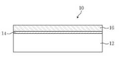
도 1은 본 발명에 따른 실라잔 물질로 표면 처리한 탄소나노튜브 코팅 기판을 보여주는 단면도이다.
도 2는 도 1의 탄소나노튜브 코팅 기판의 제조 방법에 따른 흐름도이다.
도 3 내지 도 5는 도 1의 제조 방법에 따른 각 단계를 보여주는 도면들이다.
도 6은 비교예1, 비교예2 및 실시예1에 따른 탄소나노튜브 코팅 기판의 면저항 특성을 나타내는 그래프이다.
도 7은 비교예3, 비교예4 및 실시예2에 따른 탄소나노튜브 코팅 기판의 면저항 특성을 나타내는 그래프이다.1 is a cross-sectional view showing a carbon nanotube coated substrate surface-treated with a silazane material according to the present invention.
FIG. 2 is a flowchart according to a method of manufacturing the carbon nanotube coated substrate of FIG. 1.
3 to 5 are views showing each step according to the manufacturing method of FIG.
6 is a graph showing sheet resistance characteristics of the carbon nanotube coated substrate according to Comparative Example 1, Comparative Example 2 and Example 1. FIG.
7 is a graph showing sheet resistance characteristics of carbon nanotube coated substrates according to Comparative Example 3, Comparative Example 4, and Example 2. FIG.
하기의 설명에서는 본 발명의 실시예에 따른 동작을 이해하는데 필요한 부분만이 설명되며, 그 이외 부분의 설명은 본 발명의 요지를 흩트리지 않도록 생략될 것이라는 것을 유의하여야 한다.In the following description, only parts necessary for understanding the operation according to the embodiment of the present invention will be described, it should be noted that the description of other parts will be omitted so as not to distract from the gist of the present invention.
또한 이하에서 설명되는 본 명세서 및 청구범위에 사용된 용어나 단어는 통상적이거나 사전적인 의미로 한정해서 해석되어서는 아니 되며, 발명자는 그 자신의 발명을 가장 최선의 방법으로 설명하기 위해 용어의 개념으로 적절하게 정의할 수 있다는 원칙에 입각하여 본 발명의 기술적 사상에 부합하는 의미와 개념으로 해석되어야만 한다. 따라서 본 명세서에 기재된 실시예와 도면에 도시된 구성은 본 발명의 바람직한 하나의 실시예에 불과할 뿐이고, 본 발명의 기술적 사상을 모두 대변하는 것은 아니므로, 본 출원시점에 있어서 이들을 대체할 수 있는 다양한 균등물과 변형예들이 있을 수 있음을 이해하여야 한다.Also, the terms and words used in the present specification and claims should not be construed to be limited to ordinary or dictionary meanings, and the inventor is not limited to the concept of terms in order to describe his invention in the best way. It should be construed in accordance with the meaning and concept consistent with the technical idea of the present invention based on the principle that it can be properly defined. Therefore, the embodiments described in the present specification and the configurations shown in the drawings are merely one preferred embodiment of the present invention, and not all of the technical ideas of the present invention are described. Therefore, It is to be understood that equivalents and modifications are possible.
이하, 첨부 도면을 참조하여 본 발명의 실시예를 보다 상세하게 설명하고자 한다.Hereinafter, embodiments of the present invention will be described in detail with reference to the accompanying drawings.
도 1은 본 발명에 따른 실라잔 물질로 표면 처리한 탄소나노튜브 코팅 기판을 보여주는 단면도이다.1 is a cross-sectional view showing a carbon nanotube coated substrate surface-treated with a silazane material according to the present invention.
도 1을 참조하면, 본 발명에 따른 탄소나노튜브 코팅 기판(10)은 베이스 기판(12)과, 베이스 기판(12) 위에 차례로 형성된 표면 처리막(14) 및 탄소나노튜브 전도막(16)을 포함하여 구성된다. 이때 표면 처리막(14)은 실라잔 물질로 베이스 기판(12)의 표면을 처리하여 형성한다. 그리고 탄소나노튜브 전도막(16)은 탄소나노튜브 용액을 베이스 기판(12)에 코팅하여 표면 처리막(14) 위에 형성한다.Referring to FIG. 1, the carbon nanotube coated
특히 표면 처리막(14)은 베이스 기판(12)과 탄소나노튜브 전도막(16) 사이에 개재되어 탄소나노튜브 전도막(16)의 베이스 기판(12)에 대한 접착력을 향상시켜 탄소나노튜브를 코팅한 이후에 진행되는 세척 공정에서 베이스 기판(12)에 코팅된 탄소나노튜브가 떨어져 나가는 문제를 해소할 수 있다. 또한 표면 처리막(14)을 매개로 베이스 기판(12) 위에 탄소나노튜브 전도막(16)을 형성함으로써, 기존의 탄소나노튜브 코팅 기판에 비해서 아주 낮은 면저항 특성과 같은 전기전도성을 개선할 수 있다.In particular, the
이와 같은 본 발명에 따른 탄소나노튜브 코팅 기판(10)의 제조 방법에 대해서 도 1 내지 도 5를 참조하여 설명하면 다음과 같다. 여기서 도 2는 도 1의 탄소나노튜브 코팅 기판의 제조 방법에 따른 흐름도이다. 도 3 내지 도 5는 도 1의 제조 방법에 따른 각 단계를 보여주는 도면들이다.Such a method of manufacturing the carbon nanotube coated
먼저 도 3에 도시된 바와 같이, S21단계에서 탄소나노튜브 코팅 기판으로 제조할 베이스 기판(12)을 준비한다. 이때 베이스 기판(12)으로는 유리, 석영(quartz), 글라스 웨이퍼, 실리콘 웨이퍼, 투명 플라스틱 기판, 불투명 플라스틱 기판, 투명 고분자 필름, 불투명 고분자 필름 등이 사용될 수 있으며, 이것에 한정되는 것은 아니다.First, as shown in Figure 3, in step S21 to prepare a
다음으로 도 4에 도시된 바와 같이, S23단계에서 베이스 기판(12)을 실라잔 물질로 표면 처리하여 베이스 기판(12)의 표면에 표면 처리막(14)을 형성한다. 이때 표면 처리막(14)은 일정 두께를 갖는 막으로 형성되거나, 실라잔 물질의 단분자막(monolayer)으로 형성될 수 있다. 실라잔 물질은 헥사메틸디실라잔(hexamethyldisilazane; HMDS)을 포함할 수 있으며, 이것에 한정되는 것은 아니다. 이와 같은 HDMS를 이용한 표면 처리 방법으로는 기상 처리 방법 또는 액상 처리 방법이 사용될 수 있다. 기상 처리 방법은 HMDS 증기를 베이스 기판(12) 위에 공급하여 베이스 기판(12)을 가열하여 처리하는 방법이다. 액상 처리 방법은 베이스 기판(12)에 HMDS 용액을 스핀 코팅, 딥 코팅 방법으로 코팅하고 가열하는 방법이 있다. HMDS를 이용한 표면 처리 시 베이스 기판(12)의 온도는 HMDS가 반응할 수 있도록, 60℃ 이상으로 유지하는 것이 바람직하다. 예컨대 베이스 기판(12)의 온도를 60 내지 200℃로 유지할 수 있다. 또한 HDMS를 이용한 표면 처리 방법으로는 기상 처리와 액상 처리를 함께 수행하는 것이 바람직하다.Next, as shown in FIG. 4, in step S23, the
한편 표면 처리막(14)을 형성하기 전에 베이스 기판(12)을 손상시키지 않는 범위에서, 베이스 기판(12)에 대한 전처리 공정을 선택적으로 수행할 수 있다. 전처리 공정은 산 처리, 염기 처리, 플라즈마 처리, 오존 처리를 포함할 수 있다. 이와 같은 전처리 공정을 통하여 베이스 기판(12)의 표면을 세정하여 표면 처리 효율을 향상시키고, 수산기 또는 카르복시기 등과 같은 반응성 작용기를 도입할 수 있다.On the other hand, before forming the
다음으로 도 5에 도시된 바와 같이, S25단계에서 표면 처리막(14)이 형성된 베이스 기판(12)에 탄소나노튜브 용액을 코팅하여 탄소나노튜브 층(16a)을 형성한다. 이때 탄소나노튜브 층(16a)은 스핀 코팅, 딥 코팅, 드롭핑, 스프레이 코팅, 솔루션 케스팅, 롤 코팅, 그라비아 코팅 중에 하나의 방법으로 형성할 수 있다. 이때 탄소나노튜브 용액은 단일벽 탄소나노튜브, 기능화된 단일벽 탄소나노튜브, 이중벽 탄소나노튜브, 기능화된 이중벽 탄소나노튜브, 다중벽 탄소나노튜브 및 기능화된 다중벽 탄소나노튜브 중에 적어도 하나를 포함한다. 탄소나노튜브는 SDBS, SDS, LDS, CTAB, DTAB, PVP, Triton X-series, Brij-series, Tween-series, poly(acrylic acid), polyvinyl alcohol 등 수용액계 계면활성제를 이용하여 방법, NMP(1-methyl pyrrolidone), DMF, DCE, THF 등으로 구성된 유기용매를 이용하는 방법을 포함하여, 기타 다양한 방법으로 형성될 수 있다. 이때 탄소나노튜브 층(16a)은 수nm 내지 수십nm의 두께로 형성할 수 있다.Next, as shown in FIG. 5, in step S25, the carbon nanotube solution is coated on the
그리고 S27단계에서 탄소나노튜브가 코팅된 베이스 기판(12)을 세척함으로써, 도 1에 도시된 바와 같은 탄소나노튜브 전도막(16)이 형성된 탄소나노튜브 코팅 기판(10)을 제조할 수 있다. 즉 탄소나노튜브 층(도 5의 16a)에 포함된 분산제를 제거하기 위해서 증류수로 세척한 후 건조시킴으로써, 탄소나노튜브 전도막(16)이 형성된 탄소나노튜브 코팅 기판(10)을 제조할 수 있다.In addition, by cleaning the carbon nanotube-coated
이와 같은 본 발명의 탄소나노튜브 코팅 기판(10)의 제조 방법에 따르면, 베이스 기판(12)을 HMDS와 같은 실라잔 물질로 표면 처리한 이후에 탄소나노튜브 전도막(16)을 형성함으로써, 베이스 기판(12)에 손상을 주지 않으면서 탄소나노튜브 전도막(16)을 형성할 수 있다.According to the method of manufacturing the carbon nanotube coated
또한 본 발명에 따른 탄소나노튜브 코팅 기판(10)은 실라잔 물질로 표면 처리된 베이스 기판(12)에 탄소나노튜브 전도막(16)이 형성된 구조를 갖기 때문에, 후술되겠지만 도 6 및 도 7에 도시된 바와 같이, 낮은 면 저항 특성을 갖는다. 즉 본 발명에 따른 탄소나노튜브 코팅 기판(10)은 탄소나노튜브 전도막(16)의 전기전도성을 개선할 수 있다.In addition, since the carbon
이와 같은 본 발명의 제조 방법으로 제조된 탄소나노튜브 코팅 기판(10)이 향상된 물성을 갖고 있음을 확인하기 위해서 아래와 같이 시험을 실시하였다.In order to confirm that the carbon nanotube coated
비교예1, 비교예2 및 실시예1Comparative Example 1, Comparative Example 2 and Example 1
비교예1, 비교예2 및 실시예1에서는 베이스 기판으로 유리 기판을 사용하였다.In Comparative Example 1, Comparative Example 2 and Example 1, a glass substrate was used as the base substrate.
실시예1에서는 유리 기판을 아세톤, 증류수로 세척한 후, 유리 기판에 HMDS 증기를 노출시키면서 유리 기판의 온도를 100℃로 5분 동안 가열하여 표면 처리막을 형성한다. 그리고 SDBS(Sodium dodecyl benzene sulfonate)를 분산제로 하여 단일벽 탄소나노튜브 수분산액(탄소나노튜브 용액)을 제조하여 스프레이 코팅 방법으로 HMDS로 표면 처리된 유기 기판 위에 탄소나노튜브를 코팅한다. 그리고 탄소나노튜브의 분산제를 제거하기 위해 탄소나노튜브가 코팅된 기판을 증류수로 세척함으로써, 탄소나노튜브 전도막이 코팅된 실시예1에 따른 탄소나노튜브 코팅 기판을 제조하였다.In Example 1, the glass substrate is washed with acetone and distilled water, and then the temperature of the glass substrate is heated to 100 ° C. for 5 minutes while exposing HMDS vapor to the glass substrate to form a surface treatment film. In addition, a single-walled carbon nanotube dispersion (carbon nanotube solution) was prepared using SDBS (Sodium dodecyl benzene sulfonate) as a dispersant, and carbon nanotubes were coated on an organic substrate surface-treated with HMDS by a spray coating method. In addition, the carbon nanotube coated substrate according to Example 1 was coated with a carbon nanotube conductive film by washing the substrate coated with carbon nanotubes with distilled water in order to remove the dispersant of the carbon nanotubes.
비교 시편으로써, 비교예1 및 비교예2는 각각 poly(ethylenimine)(PEI), poly(acrylic acid)(PAA)로 표면처리 된 유리 기판을 이용하여 실시예1과 동일한 방법으로 탄소나노튜브 전도막을 형성하였다. 비교예5는 표면처리 하지 않은 유리 기판을 이용하여 실시예1과 동일한 방법으로 탄소나노튜브 전도막을 형성하였다. As a comparative specimen, Comparative Example 1 and Comparative Example 2 were prepared by using a glass substrate surface-treated with poly (ethylenimine) (PEI) and poly (acrylic acid) (PAA), respectively. Formed. In Comparative Example 5, a carbon nanotube conductive film was formed in the same manner as in Example 1, using the glass substrate without surface treatment.
비교예1, 비교예2 및 실시예1에 따른 탄소나노튜브 코팅 기판의 면저항 특성을 비교하면 도 6과 같다. 여기서 도 6은 비교예1, 비교예2 및 실시예1에 따른 탄소나노튜브 코팅 기판의 면저항 특성을 나타내는 그래프이다. 실시예1에 따른 유리 기판에 대해서는 면저항을 두 번 측정하였으며, 구분하기 위해서 실시예1-1과 실시예1-2로 표기하였다.Comparing the sheet resistance characteristics of the carbon nanotube coated substrate according to Comparative Example 1, Comparative Example 2 and Example 1 is as shown in FIG. 6 is a graph showing the sheet resistance characteristics of the carbon nanotube coated substrate according to Comparative Example 1, Comparative Example 2 and Example 1. About the glass substrate which concerns on Example 1, sheet resistance was measured twice and it was described as Example 1-1 and Example 1-2.
도 6을 참조하면, 비교예5의 경우 탄소나노튜브 코팅 후 분산제 세척 과정에서 코팅막이 박리되어 투과도 및 면 저항 특성을 측정할 수 없었다.Referring to FIG. 6, in the case of Comparative Example 5, the coating film was peeled off during the dispersant washing process after coating the carbon nanotubes, and thus the transmittance and the surface resistance characteristics could not be measured.
실시예1에 따른 HMDS로 표면 처리된 유리 기판의 경우, PEI, PAA 처리된 비교예1 및 비교예2에 따른 유리 기판에 비해 동일 투과도에서 면 저항 값이 더 낮게 나타나는 것으로 확인할 수 있었다. 또한 실시예1에 따른 HMDS로 표면 처리된 유리 기판의 경우 86%(유리기판 포함한 투과도) 수준에서 340Ω/sq로 아주 낮은 저항 특성이 나타내는 것을 확인할 수 있다.In the case of the glass substrate surface-treated with HMDS according to Example 1, it was confirmed that the surface resistance value was lower at the same transmittance than the glass substrates according to PEI and PAA-treated Comparative Examples 1 and 2. In addition, in the case of the glass substrate surface-treated with the HMDS according to Example 1, it can be seen that very low resistance characteristics are exhibited at 340Ω / sq at the level of 86% (transmittance including the glass substrate).
비교예3, 비교예4 및 실시예2Comparative Example 3, Comparative Example 4 and Example 2
비교예3, 비교예4 및 실시예2에서는 베이스 기판으로 PET 기판을 사용하였다.In Comparative Example 3, Comparative Example 4 and Example 2, a PET substrate was used as the base substrate.
실시예1에서는 PET 기판을 증류수로 세척하고 PET 기판에 상압 플라즈마 처리한 한 후, HMDS 증기를 PET 기판에 노출시키면서 PET 기판의 온도를 100℃로 5분 동안 가열하여 표면 처리막을 형성한다. 그리고 SDBS(Sodium dodecyl benzene sulfonate)를 분산제로 하여 단일벽 탄소나노튜브 수분산액(탄소나노튜브 용액)을 제조하여 스프레이 코팅 방법으로 HMDS 표면처리 된 PET 기판 위에 탄소나노튜브를 코팅한다. 그리고 탄소나노튜브의 분산제를 제거하기 위해 탄소나노튜브가 코팅된 PET 기판을 증류수로 세척함으로써, 탄소나노튜브 전도막이 코팅된 실시예2에 따른 탄소나노튜브 코팅 기판을 제조하였다.In Example 1, the PET substrate is washed with distilled water and subjected to atmospheric plasma treatment on the PET substrate. Then, the surface of the PET substrate is heated to 100 ° C. for 5 minutes while exposing the HMDS vapor to the PET substrate. In addition, a single-walled carbon nanotube dispersion (carbon nanotube solution) was prepared using SDBS (sodium dodecyl benzene sulfonate) as a dispersant, and the carbon nanotubes were coated on the HMDS surface-treated PET substrate by a spray coating method. In addition, the carbon nanotube coated substrate according to Example 2 having the carbon nanotube conductive film coated thereon was prepared by washing the carbon nanotube coated PET substrate with distilled water to remove the carbon nanotube dispersant.
비교 시편으로써, 비교예3 및 비교예4는 각각 표면 처리 하지 않은 PET 기판, poly(acrylic acid)(PAA)로 표면 처리 된 PET 기판을 이용하여 실시예2와 동일한 방법으로 탄소나노튜브 전도막을 형성하였다.As a comparative specimen, Comparative Example 3 and Comparative Example 4 formed a carbon nanotube conductive film in the same manner as in Example 2, using a PET substrate surface-treated with poly (acrylic acid) (PAA) and a surface-treated PET substrate, respectively. It was.
비교예3, 비교예4 및 실시예2에 따른 탄소나노튜브 코팅 기판의 면 저항 특성을 비교하면 도 7과 같다. 여기서 도 7은 비교예3, 비교예4 및 실시예2에 따른 탄소나노튜브 코팅 기판의 면 저항 특성을 나타내는 그래프이다.When comparing the sheet resistance characteristics of the carbon nanotube coating substrate according to Comparative Example 3, Comparative Example 4 and Example 2 is as shown in FIG. 7 is a graph showing the sheet resistance characteristics of the carbon nanotube coated substrate according to Comparative Example 3, Comparative Example 4 and Example 2.
도 7을 참조하면, 실시예2에 따른 HMDS로 표면 처리된 PET 기판의 경우, 비교예3 및 비교예4에 따른 PET 기판에 비해 동일 투과도에서 면 저항 값이 더 낮게 나타나는 것으로 확인할 수 있었다.Referring to FIG. 7, the PET substrate surface-treated with HMDS according to Example 2 showed lower surface resistance values at the same transmittance than the PET substrates according to Comparative Examples 3 and 4.
한편, 본 명세서와 도면에 개시된 본 발명의 실시예들은 이해를 돕기 위해 특정 예를 제시한 것에 지나지 않으며, 본 발명의 범위를 한정하고자 하는 것은 아니다. 여기에 개시된 실시예들 이외에도 본 발명의 기술적 사상에 바탕을 둔 다른 변형예들이 실시 가능하다는 것은, 본 발명이 속하는 기술분야에서 통상의 지식을 가진 자에게 자명한 것이다.It should be noted that the embodiments of the present invention disclosed in the present specification and drawings are only illustrative of specific examples for the purpose of understanding and are not intended to limit the scope of the present invention. In addition to the embodiments disclosed herein, it is apparent to those skilled in the art that other modifications based on the technical idea of the present invention may be implemented.
10 : 탄소나노튜브 코팅 기판
12 : 베이스 기판
14 : 표면 처리막
16 : 탄소나노튜브 전도막10: carbon nanotube coating substrate
12: base substrate
14: surface treatment film
16: carbon nanotube conductive film
Claims (8)
Translated fromKorean상기 표면 처리막 위에 탄소나노튜브 용액을 코팅하여 탄소나노튜브 전도막을 형성하는 코팅 단계; 를 포함하고,
상기 표면 처리 단계에서,
상기 실라잔 물질은 헥사메틸디실라잔(hexamethyldisilazane; HMDS)을 포함하고,
상기 코팅 단계에서,
상기 베이스 기판의 온도를 60℃ 이상으로 유지하는 것을 특징으로 하는 실라잔 물질로 표면 처리한 탄소나노튜브 코팅 기판의 제조 방법.A surface treatment step of surface treating the surface of the base substrate with a silazane material to form a surface treatment film;
Coating a carbon nanotube solution on the surface treatment film to form a carbon nanotube conductive film; Lt; / RTI >
In the surface treatment step,
The silazane material comprises hexamethyldisilazane (HMDS),
In the coating step,
The method of manufacturing a carbon nanotube coated substrate surface-treated with a silazane material, characterized in that to maintain the temperature of the base substrate at 60 ℃ or more.
상기 베이스 기판을 산 처리, 염기 처리, 플라즈마 처리 또는 오존 처리를 수행하는 단계;
를 더 포함하는 것을 특징으로 하는 실라잔 물질로 표면 처리한 탄소나노튜브 코팅 기판의 제조 방법.The method according to claim 4, which is carried out before the surface treatment step,
Performing an acid treatment, a base treatment, a plasma treatment, or an ozone treatment on the base substrate;
Method for producing a carbon nanotube coated substrate surface-treated with a silazane material, characterized in that it further comprises.
상기 탄소나노튜브 전도막은 스핀 코팅(spin coating), 딥 코팅(dip coating), 드롭핑(dropping), 스프레이 코팅(spray coating), 솔루션 케스팅(solution casting), 롤 코팅(roll coating), 그라비아 코팅(gravure coating) 중에 하나의 방법으로 형성하는 것을 특징으로 하는 실라잔 물질로 표면 처리한 탄소나노튜브 코팅 기판의 제조 방법.The method of claim 4, wherein in the coating step,
The carbon nanotube conductive film may include spin coating, dip coating, dropping, spray coating, solution casting, roll coating, and gravure coating. A method for producing a carbon nanotube coated substrate surface-treated with a silazane material, characterized in that it is formed by one of gravure coating.
Priority Applications (1)
| Application Number | Priority Date | Filing Date | Title |
|---|---|---|---|
| KR1020110083380AKR101276060B1 (en) | 2011-08-22 | 2011-08-22 | Substrate coated carbon nanotube(CNT) and manufacturing method thereof |
Applications Claiming Priority (1)
| Application Number | Priority Date | Filing Date | Title |
|---|---|---|---|
| KR1020110083380AKR101276060B1 (en) | 2011-08-22 | 2011-08-22 | Substrate coated carbon nanotube(CNT) and manufacturing method thereof |
Publications (2)
| Publication Number | Publication Date |
|---|---|
| KR20130021078A KR20130021078A (en) | 2013-03-05 |
| KR101276060B1true KR101276060B1 (en) | 2013-06-17 |
Family
ID=48174110
Family Applications (1)
| Application Number | Title | Priority Date | Filing Date |
|---|---|---|---|
| KR1020110083380AExpired - Fee RelatedKR101276060B1 (en) | 2011-08-22 | 2011-08-22 | Substrate coated carbon nanotube(CNT) and manufacturing method thereof |
Country Status (1)
| Country | Link |
|---|---|
| KR (1) | KR101276060B1 (en) |
Citations (1)
| Publication number | Priority date | Publication date | Assignee | Title |
|---|---|---|---|---|
| KR20110036543A (en)* | 2008-06-09 | 2011-04-07 | 유니다임, 인크. | Improved CNC / Top Coating Process for Fabrication of Transplant Conductors |
- 2011
- 2011-08-22KRKR1020110083380Apatent/KR101276060B1/ennot_activeExpired - Fee Related
Patent Citations (1)
| Publication number | Priority date | Publication date | Assignee | Title |
|---|---|---|---|---|
| KR20110036543A (en)* | 2008-06-09 | 2011-04-07 | 유니다임, 인크. | Improved CNC / Top Coating Process for Fabrication of Transplant Conductors |
Also Published As
| Publication number | Publication date |
|---|---|
| KR20130021078A (en) | 2013-03-05 |
Similar Documents
| Publication | Publication Date | Title |
|---|---|---|
| KR101143304B1 (en) | Substrate improved adhesion stability of carbon nanotube conductive film and manufacturing method thereof | |
| JP6164617B2 (en) | Method for producing conductive thin film and conductive thin film produced by the method | |
| CN104112777B (en) | Thin film transistor (TFT) and preparation method thereof | |
| KR20120006458A (en) | Conductive paint composition and manufacturing method of the conductive film using the same | |
| Kim et al. | Industrially feasible approach to transparent, flexible, and conductive carbon nanotube films: cellulose-assisted film deposition followed by solution and photonic processing | |
| CN105161621A (en) | Film patterning preparation method | |
| CN104576394B (en) | A kind of large area prints the preparation method of independent carbon nano-tube film transistor | |
| KR101592371B1 (en) | Method for transferring highly conductive pedot:pss based electrode | |
| KR101371289B1 (en) | Preparing method of carbon nano thin film | |
| JP2016126847A (en) | Production method of transparent conductive film and transparent conductive laminate | |
| KR101186801B1 (en) | Post treatment processing method and its formulation of polymer solution for electric and thermal conductive thin film | |
| KR101276060B1 (en) | Substrate coated carbon nanotube(CNT) and manufacturing method thereof | |
| KR101172688B1 (en) | Method for manufacturing carbon nanotube thin film by substrate pretreatment using polyelectrolyte and the carbon nanotube thin film | |
| CN102320752B (en) | Patterning method for material | |
| KR101154869B1 (en) | Carbon nanotube transparent film with low resistance and high conductivity, and manufacturing method thereof | |
| Li et al. | Facile method for enhancing conductivity of printed carbon nanotubes electrode via simple rinsing process | |
| KR101999488B1 (en) | Method for removal of polymer residues on a graphene film | |
| JP2023115123A (en) | Material that improving performance of printable electronics and a base material | |
| RU2577174C1 (en) | Coating for photovoltaic cell and method of making same | |
| KR101438581B1 (en) | Method for forming thin film layer, manufacturing field effect transistor and manufacturing display | |
| CN113072036A (en) | Preparation method of super-hydrophobic carbon nanotube film | |
| US20100055562A1 (en) | Nanowire layer adhesion on a substrate | |
| Rashid et al. | Fabrication and characterization on reduced graphene oxide field effect transistor (RGOFET) based biosensor | |
| KR101154867B1 (en) | Post treatment technology and its formulation for electric thermal conductive carbon nanotube thin film | |
| WO2016181964A1 (en) | Electroconductive film, transistor, and method for producing thin film |
Legal Events
| Date | Code | Title | Description |
|---|---|---|---|
| A201 | Request for examination | ||
| PA0109 | Patent application | St.27 status event code:A-0-1-A10-A12-nap-PA0109 | |
| PA0201 | Request for examination | St.27 status event code:A-1-2-D10-D11-exm-PA0201 | |
| D13-X000 | Search requested | St.27 status event code:A-1-2-D10-D13-srh-X000 | |
| D14-X000 | Search report completed | St.27 status event code:A-1-2-D10-D14-srh-X000 | |
| PE0902 | Notice of grounds for rejection | St.27 status event code:A-1-2-D10-D21-exm-PE0902 | |
| E13-X000 | Pre-grant limitation requested | St.27 status event code:A-2-3-E10-E13-lim-X000 | |
| P11-X000 | Amendment of application requested | St.27 status event code:A-2-2-P10-P11-nap-X000 | |
| P13-X000 | Application amended | St.27 status event code:A-2-2-P10-P13-nap-X000 | |
| PG1501 | Laying open of application | St.27 status event code:A-1-1-Q10-Q12-nap-PG1501 | |
| PN2301 | Change of applicant | St.27 status event code:A-3-3-R10-R11-asn-PN2301 St.27 status event code:A-3-3-R10-R13-asn-PN2301 | |
| E701 | Decision to grant or registration of patent right | ||
| PE0701 | Decision of registration | St.27 status event code:A-1-2-D10-D22-exm-PE0701 | |
| GRNT | Written decision to grant | ||
| PR0701 | Registration of establishment | St.27 status event code:A-2-4-F10-F11-exm-PR0701 | |
| PR1002 | Payment of registration fee | Fee payment year number:1 St.27 status event code:A-2-2-U10-U11-oth-PR1002 | |
| PG1601 | Publication of registration | St.27 status event code:A-4-4-Q10-Q13-nap-PG1601 | |
| FPAY | Annual fee payment | Payment date:20151224 Year of fee payment:4 | |
| PR1001 | Payment of annual fee | Fee payment year number:4 St.27 status event code:A-4-4-U10-U11-oth-PR1001 | |
| P22-X000 | Classification modified | St.27 status event code:A-4-4-P10-P22-nap-X000 | |
| PC1903 | Unpaid annual fee | Not in force date:20170605 Payment event data comment text:Termination Category : DEFAULT_OF_REGISTRATION_FEE St.27 status event code:A-4-4-U10-U13-oth-PC1903 | |
| FPAY | Annual fee payment | Payment date:20180223 Year of fee payment:5 | |
| K11-X000 | Ip right revival requested | St.27 status event code:A-6-4-K10-K11-oth-X000 | |
| PC1903 | Unpaid annual fee | Ip right cessation event data comment text:Termination Category : DEFAULT_OF_REGISTRATION_FEE Not in force date:20170605 St.27 status event code:N-4-6-H10-H13-oth-PC1903 | |
| PR0401 | Registration of restoration | St.27 status event code:A-6-4-K10-K13-oth-PR0401 | |
| PR1001 | Payment of annual fee | Fee payment year number:5 St.27 status event code:A-4-4-U10-U11-oth-PR1001 | |
| R401 | Registration of restoration | ||
| PN2301 | Change of applicant | St.27 status event code:A-5-5-R10-R11-asn-PN2301 | |
| PN2301 | Change of applicant | St.27 status event code:A-5-5-R10-R14-asn-PN2301 | |
| FPAY | Annual fee payment | Payment date:20180604 Year of fee payment:6 | |
| PR1001 | Payment of annual fee | Fee payment year number:6 St.27 status event code:A-4-4-U10-U11-oth-PR1001 | |
| P14-X000 | Amendment of ip right document requested | St.27 status event code:A-5-5-P10-P14-nap-X000 | |
| R18-X000 | Changes to party contact information recorded | St.27 status event code:A-5-5-R10-R18-oth-X000 | |
| FPAY | Annual fee payment | Payment date:20190603 Year of fee payment:7 | |
| PR1001 | Payment of annual fee | Fee payment year number:7 St.27 status event code:A-4-4-U10-U11-oth-PR1001 | |
| P14-X000 | Amendment of ip right document requested | St.27 status event code:A-5-5-P10-P14-nap-X000 | |
| PR1001 | Payment of annual fee | Fee payment year number:8 St.27 status event code:A-4-4-U10-U11-oth-PR1001 | |
| R18-X000 | Changes to party contact information recorded | St.27 status event code:A-5-5-R10-R18-oth-X000 | |
| P14-X000 | Amendment of ip right document requested | St.27 status event code:A-5-5-P10-P14-nap-X000 | |
| PR1001 | Payment of annual fee | Fee payment year number:9 St.27 status event code:A-4-4-U10-U11-oth-PR1001 | |
| P14-X000 | Amendment of ip right document requested | St.27 status event code:A-5-5-P10-P14-nap-X000 | |
| R18-X000 | Changes to party contact information recorded | St.27 status event code:A-5-5-R10-R18-oth-X000 | |
| PR1001 | Payment of annual fee | Fee payment year number:10 St.27 status event code:A-4-4-U10-U11-oth-PR1001 | |
| P14-X000 | Amendment of ip right document requested | St.27 status event code:A-5-5-P10-P14-nap-X000 | |
| PN2301 | Change of applicant | St.27 status event code:A-5-5-R10-R11-asn-PN2301 St.27 status event code:A-5-5-R10-R13-asn-PN2301 | |
| PN2301 | Change of applicant | St.27 status event code:A-5-5-R10-R11-asn-PN2301 St.27 status event code:A-5-5-R10-R13-asn-PN2301 | |
| PR1001 | Payment of annual fee | Fee payment year number:11 St.27 status event code:A-4-4-U10-U11-oth-PR1001 | |
| PC1903 | Unpaid annual fee | Not in force date:20240605 Payment event data comment text:Termination Category : DEFAULT_OF_REGISTRATION_FEE St.27 status event code:A-4-4-U10-U13-oth-PC1903 | |
| PC1903 | Unpaid annual fee | Ip right cessation event data comment text:Termination Category : DEFAULT_OF_REGISTRATION_FEE Not in force date:20240605 St.27 status event code:N-4-6-H10-H13-oth-PC1903 |