KR101273567B1 - A counter electrodes for dye-sensitized solar cells and preparation method thereof - Google Patents
A counter electrodes for dye-sensitized solar cells and preparation method thereofDownload PDFInfo
- Publication number
- KR101273567B1 KR101273567B1KR1020110122385AKR20110122385AKR101273567B1KR 101273567 B1KR101273567 B1KR 101273567B1KR 1020110122385 AKR1020110122385 AKR 1020110122385AKR 20110122385 AKR20110122385 AKR 20110122385AKR 101273567 B1KR101273567 B1KR 101273567B1
- Authority
- KR
- South Korea
- Prior art keywords
- substrate
- oxide
- dye
- carbon
- sensitized solar
- Prior art date
- Legal status (The legal status is an assumption and is not a legal conclusion. Google has not performed a legal analysis and makes no representation as to the accuracy of the status listed.)
- Expired - Fee Related
Links
Images


Classifications
- H—ELECTRICITY
- H01—ELECTRIC ELEMENTS
- H01G—CAPACITORS; CAPACITORS, RECTIFIERS, DETECTORS, SWITCHING DEVICES, LIGHT-SENSITIVE OR TEMPERATURE-SENSITIVE DEVICES OF THE ELECTROLYTIC TYPE
- H01G9/00—Electrolytic capacitors, rectifiers, detectors, switching devices, light-sensitive or temperature-sensitive devices; Processes of their manufacture
- H01G9/20—Light-sensitive devices
- H01G9/2022—Light-sensitive devices characterized by he counter electrode
- H—ELECTRICITY
- H10—SEMICONDUCTOR DEVICES; ELECTRIC SOLID-STATE DEVICES NOT OTHERWISE PROVIDED FOR
- H10F—INORGANIC SEMICONDUCTOR DEVICES SENSITIVE TO INFRARED RADIATION, LIGHT, ELECTROMAGNETIC RADIATION OF SHORTER WAVELENGTH OR CORPUSCULAR RADIATION
- H10F10/00—Individual photovoltaic cells, e.g. solar cells
- G—PHYSICS
- G02—OPTICS
- G02B—OPTICAL ELEMENTS, SYSTEMS OR APPARATUS
- G02B6/00—Light guides; Structural details of arrangements comprising light guides and other optical elements, e.g. couplings
- G02B6/10—Light guides; Structural details of arrangements comprising light guides and other optical elements, e.g. couplings of the optical waveguide type
- G02B6/12—Light guides; Structural details of arrangements comprising light guides and other optical elements, e.g. couplings of the optical waveguide type of the integrated circuit kind
- G02B6/13—Integrated optical circuits characterised by the manufacturing method
- G02B6/136—Integrated optical circuits characterised by the manufacturing method by etching
- H—ELECTRICITY
- H10—SEMICONDUCTOR DEVICES; ELECTRIC SOLID-STATE DEVICES NOT OTHERWISE PROVIDED FOR
- H10F—INORGANIC SEMICONDUCTOR DEVICES SENSITIVE TO INFRARED RADIATION, LIGHT, ELECTROMAGNETIC RADIATION OF SHORTER WAVELENGTH OR CORPUSCULAR RADIATION
- H10F71/00—Manufacture or treatment of devices covered by this subclass
- H—ELECTRICITY
- H10—SEMICONDUCTOR DEVICES; ELECTRIC SOLID-STATE DEVICES NOT OTHERWISE PROVIDED FOR
- H10F—INORGANIC SEMICONDUCTOR DEVICES SENSITIVE TO INFRARED RADIATION, LIGHT, ELECTROMAGNETIC RADIATION OF SHORTER WAVELENGTH OR CORPUSCULAR RADIATION
- H10F77/00—Constructional details of devices covered by this subclass
- H10F77/20—Electrodes
- B—PERFORMING OPERATIONS; TRANSPORTING
- B32—LAYERED PRODUCTS
- B32B—LAYERED PRODUCTS, i.e. PRODUCTS BUILT-UP OF STRATA OF FLAT OR NON-FLAT, e.g. CELLULAR OR HONEYCOMB, FORM
- B32B2457/00—Electrical equipment
- B32B2457/12—Photovoltaic modules
- B—PERFORMING OPERATIONS; TRANSPORTING
- B32—LAYERED PRODUCTS
- B32B—LAYERED PRODUCTS, i.e. PRODUCTS BUILT-UP OF STRATA OF FLAT OR NON-FLAT, e.g. CELLULAR OR HONEYCOMB, FORM
- B32B2457/00—Electrical equipment
- B32B2457/20—Displays, e.g. liquid crystal displays, plasma displays
- B—PERFORMING OPERATIONS; TRANSPORTING
- B32—LAYERED PRODUCTS
- B32B—LAYERED PRODUCTS, i.e. PRODUCTS BUILT-UP OF STRATA OF FLAT OR NON-FLAT, e.g. CELLULAR OR HONEYCOMB, FORM
- B32B37/00—Methods or apparatus for laminating, e.g. by curing or by ultrasonic bonding
- B32B37/02—Methods or apparatus for laminating, e.g. by curing or by ultrasonic bonding characterised by a sequence of laminating steps, e.g. by adding new layers at consecutive laminating stations
- B32B37/025—Transfer laminating
- H—ELECTRICITY
- H01—ELECTRIC ELEMENTS
- H01G—CAPACITORS; CAPACITORS, RECTIFIERS, DETECTORS, SWITCHING DEVICES, LIGHT-SENSITIVE OR TEMPERATURE-SENSITIVE DEVICES OF THE ELECTROLYTIC TYPE
- H01G9/00—Electrolytic capacitors, rectifiers, detectors, switching devices, light-sensitive or temperature-sensitive devices; Processes of their manufacture
- H01G9/20—Light-sensitive devices
- H01G9/2027—Light-sensitive devices comprising an oxide semiconductor electrode
- H01G9/2031—Light-sensitive devices comprising an oxide semiconductor electrode comprising titanium oxide, e.g. TiO2
- H—ELECTRICITY
- H01—ELECTRIC ELEMENTS
- H01G—CAPACITORS; CAPACITORS, RECTIFIERS, DETECTORS, SWITCHING DEVICES, LIGHT-SENSITIVE OR TEMPERATURE-SENSITIVE DEVICES OF THE ELECTROLYTIC TYPE
- H01G9/00—Electrolytic capacitors, rectifiers, detectors, switching devices, light-sensitive or temperature-sensitive devices; Processes of their manufacture
- H01G9/20—Light-sensitive devices
- H01G9/2059—Light-sensitive devices comprising an organic dye as the active light absorbing material, e.g. adsorbed on an electrode or dissolved in solution
- Y—GENERAL TAGGING OF NEW TECHNOLOGICAL DEVELOPMENTS; GENERAL TAGGING OF CROSS-SECTIONAL TECHNOLOGIES SPANNING OVER SEVERAL SECTIONS OF THE IPC; TECHNICAL SUBJECTS COVERED BY FORMER USPC CROSS-REFERENCE ART COLLECTIONS [XRACs] AND DIGESTS
- Y02—TECHNOLOGIES OR APPLICATIONS FOR MITIGATION OR ADAPTATION AGAINST CLIMATE CHANGE
- Y02E—REDUCTION OF GREENHOUSE GAS [GHG] EMISSIONS, RELATED TO ENERGY GENERATION, TRANSMISSION OR DISTRIBUTION
- Y02E10/00—Energy generation through renewable energy sources
- Y02E10/50—Photovoltaic [PV] energy
- Y02E10/52—PV systems with concentrators
- Y—GENERAL TAGGING OF NEW TECHNOLOGICAL DEVELOPMENTS; GENERAL TAGGING OF CROSS-SECTIONAL TECHNOLOGIES SPANNING OVER SEVERAL SECTIONS OF THE IPC; TECHNICAL SUBJECTS COVERED BY FORMER USPC CROSS-REFERENCE ART COLLECTIONS [XRACs] AND DIGESTS
- Y02—TECHNOLOGIES OR APPLICATIONS FOR MITIGATION OR ADAPTATION AGAINST CLIMATE CHANGE
- Y02E—REDUCTION OF GREENHOUSE GAS [GHG] EMISSIONS, RELATED TO ENERGY GENERATION, TRANSMISSION OR DISTRIBUTION
- Y02E10/00—Energy generation through renewable energy sources
- Y02E10/50—Photovoltaic [PV] energy
- Y02E10/542—Dye sensitized solar cells
Landscapes
- Engineering & Computer Science (AREA)
- Power Engineering (AREA)
- Microelectronics & Electronic Packaging (AREA)
- Physics & Mathematics (AREA)
- General Physics & Mathematics (AREA)
- Optics & Photonics (AREA)
- Hybrid Cells (AREA)
- Photovoltaic Devices (AREA)
Abstract
Translated fromKoreanDescription
Translated fromKorean본 발명은 염료감응 태양전지용 상대전극 및 이의 제조방법과, 이를 이용한 염료감응 태양전지에 관한 것이다.The present invention relates to a counter electrode for a dye-sensitized solar cell, a manufacturing method thereof, and a dye-sensitized solar cell using the same.
염료감응 태양전지(dye-sensitized photovoltaic cell)는 1991년 스위스의 그라첼(Gratzel) 등에 의하여 발표된 광전기화학 태양전지로 대표되는 것으로서, 일반적으로 가시광선을 흡수하는 감광성 염료, 넓은 밴드갭 에너지를 갖는 금속산화물 나노입자, 백금(Pt)에 의해 촉매작용을 하는 상대전극(counter electrode), 그리고 그 사이에 채워진 전해질로 구성되어 있다. 염료감응형 태양전지는 기존의 실리콘 태양전지나 화합물 반도체 태양전지에 비해 그 제작비용이 저렴하고, 유기 태양전지에 비하여 그 효율이 높으며 이 외에도 친환경적이고 여러가지 색을 구현할 수 있다는 장점을 가진다.Dye-sensitized photovoltaic cells are representative of photoelectrochemical solar cells published by Gratzel et al. In Switzerland in 1991, and are generally photosensitive dyes that absorb visible light and have broad bandgap energy. It consists of a metal oxide nanoparticle, a counter electrode catalyzed by platinum (Pt), and an electrolyte filled therebetween. Dye-sensitized solar cells have lower manufacturing costs than conventional silicon solar cells or compound semiconductor solar cells, have higher efficiency than organic solar cells, and are environmentally friendly and can realize various colors.
특히 플렉서블 염료감응 태양전지는 휴대폰, 웨어러블 PC 등 차세대 PC 산업에 필요한 전원의 자가 충전이나 옷, 모자, 자동차 유리, 건물 등에 부착해 활용할 수 있다는 점에서 더욱 관심의 초점이 되고 있다.In particular, flexible dye-sensitized solar cells have become a focus of interest because they can be used for self-charging of power required for the next-generation PC industry such as mobile phones and wearable PCs, clothes, hats, automobile glass, and buildings.
한편, 상기 염료감응 태양전지에 사용되는 상대 전극의 제작에 필요한 백금촉매는 현재 진공 공정이 필요한 스퍼터링 방법을 통해 증착을 하고 있다. 또한 종래 방법은 백금 화합물을 고온에서 소성하여 백금나노입자를 만들거나 또는 TCO 기판위에 탄소 기반 재료(카본, 카본나노튜브, 그라펜)을 올려 백금 촉매 대신 사용하여 상대전극을 제조하고 있다.On the other hand, the platinum catalyst required for the fabrication of the counter electrode used in the dye-sensitized solar cell is currently deposited through a sputtering method requiring a vacuum process. In addition, in the conventional method, a counterpart is manufactured by baking a platinum compound at high temperature to make platinum nanoparticles, or by placing a carbon-based material (carbon, carbon nanotube, graphene) on a TCO substrate and replacing the platinum catalyst.
그러나 이러한 방법에서는 고가의 TCO 전극을 사용해야 하고, 진공 공정이나 고온공정이 필요하다. 또한 상기 탄소기반 재료만을 이용할 경우, 백금보다 태양전지의 광전효율이 떨어지는 문제점 등이 발생하게 된다. 더욱이, 플라스틱 유연기판에 바로 상대전극을 만들게 되면 저온에서 모든 공정을 진행해야 하므로 전극의 특성이 떨어지는 문제점이 발생한다.
However, this method requires the use of expensive TCO electrodes and requires a vacuum process or a high temperature process. In addition, when only the carbon-based material is used, the photoelectric efficiency of the solar cell is lower than that of platinum. In addition, when the counter electrode is directly made on the plastic flexible substrate, all the processes must be performed at low temperature, thereby deteriorating the characteristics of the electrode.
상기와 같은 종래기술의 문제점을 해소하기 위하여, 본 발명의 목적은 전사법을 이용하여 촉매와 전극역할을 동시에 할 수 있는 염료감응 태양전지용 상대전극의 제조 방법을 제공하는 것이다.In order to solve the problems of the prior art as described above, an object of the present invention is to provide a method for producing a counter electrode for a dye-sensitized solar cell that can serve as a catalyst and an electrode at the same time by using a transfer method.
본 발명의 다른 목적은 상기 상대전극을 이용하여, 기판의 종류(유리기판, 유연기판, 금속기판 등)에 관계없이 염료감응 태양전지의 상대전극으로 적용하는 방법을 제공하는 것이다.Another object of the present invention is to provide a method using the counter electrode as a counter electrode of a dye-sensitized solar cell irrespective of the type of substrate (glass substrate, flexible substrate, metal substrate, etc.).
본 발명의 다른 목적은 상기 상대전극을 이용하여, 염료감응 태양전지의 저가화가 가능하면서도 높은 광전 효율을 갖는 태양전지를 제공하는 것이다.
Another object of the present invention is to provide a solar cell having a high photoelectric efficiency while being able to reduce the cost of a dye-sensitized solar cell using the counter electrode.
본 발명은 (a) 500 ℃ 이하의 온도에서 변형이 일어나지 않는 고온 내성을 가지는 제1 기판, 탄소 기반 재료와 백금 나노입자를 포함하는 다공질막, 점착층 및 제 2기판을 포함하는 A 기판을 제조하는 단계; 및The present invention provides a substrate comprising (a) a first substrate having a high temperature resistance that does not occur at a temperature of 500 ° C. or lower, a porous membrane including a carbon-based material and platinum nanoparticles, an adhesive layer, and a second substrate. Making; And
(b) 전사법으로 상기 A 기판에서 상기 고온 내성을 가지는 제1 기판을 분리하고 상기 다공질막 및 점착층을 제 2기판으로 이동시켜, 제 2기판, 상기 제 2기판 위에 형성된 점착층 및 다공질막을 포함하는 B 기판을 제조하는 단계;(b) separating the first substrate having the high temperature resistance from the A substrate by the transfer method and moving the porous film and the adhesive layer to the second substrate, thereby forming the second substrate and the adhesive layer and the porous film formed on the second substrate. Manufacturing a B substrate comprising;
를 포함하는 염료감응 태양전지용 상대전극의 제조방법을 제공한다.It provides a method for producing a counter electrode for a dye-sensitized solar cell comprising a.
또한 본 발명은 상술한 방법으로 제조되며, 제2 기판, 상기 제 2 기판의 일면에 형성된 점착층, 및 상기 점착층 위에 형성된 탄소기반 재료와 백금 나노입자를 포함하는 다공질막을 포함하며, 상기 제2 기판은 금속기판, 유리기판, 유연 기판인 플라스틱 기판, 직물 기판, 또는 세라믹 기판인 염료감응 태양전지용 상대전극을 제공한다.In another aspect, the present invention is prepared by the method described above, and includes a porous film including a second substrate, an adhesive layer formed on one surface of the second substrate, and a carbon-based material and platinum nanoparticles formed on the adhesive layer, the second The substrate provides a counter electrode for a dye-sensitized solar cell, which is a metal substrate, a glass substrate, a plastic substrate that is a flexible substrate, a fabric substrate, or a ceramic substrate.
또한 본 발명은 상기 플렉서블 상대전극, 상기 상대전극과 소정의 간격을 두고 서로 마주보도록 대향 배치된 광전극, 및 상기 상대전극과 광전극 사이의 공간을 충진하는 전해질을 포함하는 플렉서블 염료감응 태양전지를 제공한다.
The present invention also provides a flexible dye-sensitized solar cell including the flexible counter electrode, a photoelectrode disposed to face each other at a predetermined interval to face the counter electrode, and an electrolyte filling a space between the counter electrode and the photoelectrode. to provide.
이하에서 본 발명을 상세하게 설명한다.Hereinafter, the present invention will be described in detail.
상술한 바와 같이, 일반적으로 플렉서블 반도체 상대전극을 제조하는 종래 방법으로는 투명전도성물질 (TCO: transparent conducting oxide)이 코팅된 기판 위에 백금을 증착 방법을 이용하여 만들거나, TCO 기판위에 촉매 특성이 있는 탄소기반 재료를 백금 대신 사용하는 방법이 알려져 있다. 그러나 이러한 방법에서는 고가의 TCO 전극을 사용하고 진공 공정이 필요하며, 탄소기반 재료 산화물을 이용하는 경우에는 백금보다 태양전지의 광전효율이 떨어지는 문제점 등이 발생하였다.As described above, in general, a conventional method for manufacturing a flexible semiconductor counter electrode is made by depositing platinum on a transparent conducting oxide (TCO) coated substrate or using a catalytic property on the TCO substrate. It is known to use carbon-based materials instead of platinum. However, such a method requires an expensive TCO electrode and requires a vacuum process, and when a carbon-based material oxide is used, photovoltaic efficiency of a solar cell is lower than that of platinum.
본 발명에서 제시된 구조를 이용하면, 간단한 공정으로 TCO 가 필요없는 기판 위에 우수한 광전효율을 갖는 염료감응 태양전지의 상대전극을 제공할 수 있다.Using the structure proposed in the present invention, it is possible to provide a counter electrode of a dye-sensitized solar cell having excellent photoelectric efficiency on a substrate which does not require TCO in a simple process.
따라서, 본 발명에서는 촉매특성이 있는 탄소기반 재료와 백금을 포함하도록 하여, 광전효율이 우수하고, TCO를 사용하지 않으며 진공공정이 불필요하여 가격이 저렴할 뿐 아니라, 기판에 관계없이 적용이 가능한 상대전극의 제조방법을 제공하고자 한다.Therefore, the present invention includes a carbon-based material and platinum having catalytic properties, and has excellent photoelectric efficiency, does not use TCO, does not require a vacuum process, and is inexpensive, and can be applied regardless of the substrate. To provide a method of manufacturing.
또한, 상기 기판 중에서도 유연성이 있는 기판에 적용을 하면 휴대폰, 웨어러블 PC 등 차세대 PC 산업 등에 적용하기에 더욱 효과적이다.In addition, if applied to a flexible substrate among the substrates, it is more effective to apply to the next-generation PC industry, such as a mobile phone, a wearable PC.
그러면, 첨부한 도면을 참조하여, 본 발명이 속하는 기술 분야에서 통상의 지식을 가진 자가 용이하게 실시할 수 있도록 본 발명의 바람직한 실시예를 설명하기로 한다. 이때 본 발명이 속하는 기술 분야에서 통상의 지식을 가진 자가 용이하게 이해할 수 있는 바와 같이, 후술하는 실시예 본 발명을 단지 예시하기 위한 것이며, 본 발명의 개념과 범위를 벗어나지 않는 한도 내에서 다양한 형태로 변형될 수 있다. 가능한 한 동일하거나 유사한 부분은 도면에서 동일한 인용부호를 사용하여 나타낸다.Hereinafter, preferred embodiments of the present invention will be described with reference to the accompanying drawings, so that those skilled in the art can easily carry out the present invention. At this time, as can be easily understood by those skilled in the art to which the present invention pertains, the following embodiments are only intended to illustrate the present invention, in various forms without departing from the concept and scope of the present invention. It can be modified. Where possible, the same or similar parts are represented using the same reference numerals in the drawings.
또한 본 발명에 있어서, 어느 부분이 다른 부분의 "위에" 또는 "상부"에 있다고 언급하는 경우, 이는 바로 다른 부분의 위에 있을 수 있거나 그 사이에 다른 부분이 수반될 수 있다. 대조적으로 어느 부분이 다른 부분의 "바로 위에" 있다고 언급하는 경우, 그 사이에 다른 부분이 수반되지 않는다.Also in the present invention, when referring to a portion as "on" or "top" of another portion, it may be directly on top of another portion or may be accompanied by another portion therebetween. In contrast, when a part is mentioned as "directly above" another part, no other part is involved between them.
또한 본 발명에 있어서, 제1, 및 제2 등의 용어들은 다양한 부분, 성분, 영역, 층 및/또는 섹션들을 구분하여 설명하기 위해 사용되지만, 이들에 한정되지 않는다. 따라서 이들 용어들은 어느 부분, 성분, 영역, 층 또는 섹션을 다른 부분, 성분, 영역, 층 또는 섹션과 구별하기 위해서만 사용된다.In addition, in the present invention, terms such as first and second are used to describe various parts, components, regions, layers, and / or sections separately, but are not limited thereto. Thus, these terms are only used to distinguish one part, component, region, layer or section from another part, component, region, layer or section.
여기서 사용되는 전문 용어는 단지 특정 실시예를 언급하기 위한 것이며, 본 발명을 한정하는 것을 의도하지 않는다. 명세서에서 사용되는 "포함하는"의 의미는 특정 특성, 영역, 정수, 단계, 동작, 요소 및/또는 성분을 구체화하며, 다른 특성, 영역, 정수, 단계, 동작, 요소 및/또는 성분의 존재나 부가를 제외시키는 것은 아니다.The terminology used herein is for the purpose of describing particular embodiments only and is not intended to limit the invention. Means that a particular feature, region, integer, step, operation, element and / or component is specified and that the presence or absence of other features, regions, integers, steps, operations, elements, and / It does not exclude addition.
본 발명의 명세서에 기재된 "나노"라는 용어는 나노 스케일을 의미하며, 마이크로 단위를 포함할 수도 있다. 또한, 명세서에 기재된 "나노 입자"라는 용어는 나노 스케일을 가진 모든 형태의 입자를 포함한다.The term "nano" described in the specification of the present invention means nano-scale, and may include micro units. In addition, the term "nanoparticle" as described herein includes all types of particles having a nanoscale.
본 발명의 명세서에서, "상대전극"은 염료감응 태양전지에 사용될 수 있는"상대 전극"을 의미한다. 또한 본 발명에서 "탄소기반 재료와 백금 나노입자를 포함하는 다공질막"은 "상대전극으로 사용하는 전극과 촉매층"을 의미한다.In the context of the present invention, "relative electrode" means "relative electrode" which can be used in dye-sensitized solar cells. In addition, in the present invention, "porous membrane including carbon-based material and platinum nanoparticles" means "electrode and catalyst layer used as a counter electrode."
한편, 본 발명의 바람직한 구현예에 따르면, (a) 500 ℃ 이하의 온도에서 변형이 일어나지 않는 고온 내성을 가지는 제1 기판, 탄소 기반 재료와 백금 나노입자를 포함하는 다공질막, 점착층 및 제 2기판을 포함하는 A 기판을 제조하는 단계; 및 (b) 전사법으로 상기 A 기판에서 고온 내성을 가지는 제1 기판을 분리하고 상기 다공질막 및 점착층을 제 2기판으로 이동시켜, 제 2기판, 상기 제 2기판 위에 형성된 점착층 및 다공질막을 포함하는 B 기판을 제조하는 단계;를 포함하는 염료감응 태양전지용 상대전극의 제조방법이 제공된다.On the other hand, according to a preferred embodiment of the present invention, (a) a first substrate having a high temperature resistance that does not occur deformation at a temperature of 500 ℃ or less, a porous membrane comprising a carbon-based material and platinum nanoparticles, an adhesive layer and a second Manufacturing an A substrate comprising a substrate; And (b) separating the first substrate having high temperature resistance from the A substrate by the transfer method and moving the porous membrane and the adhesive layer to the second substrate, thereby forming the second substrate, the adhesive layer and the porous membrane formed on the second substrate. A method of manufacturing a counter electrode for a dye-sensitized solar cell is provided.
먼저, 본 발명에서 제1 기판은 400 내지 500 ℃까지의 고온을 견딜 수 있는 고온 내성 기판을 의미하며, 온도에 한정 되는 것이 아니고 탄소기반 재료와 백금 나노입자를 포함하는 다공질막이 고온에서 소성하여 막의 안정성과 높은 전도도를 나타내는 온도에 변형이 일어나지 않는 특징을 갖는 것을 말한다. 또한 상기 제2 기판은 점착층이 붙을 수 있는 기판을 의미하며, 이것은 점착층이 붙을 수 있는 것이면 종류에 무관하게 대체적으로 모두 사용이 가능하다.First, in the present invention, the first substrate means a high temperature resistant substrate capable of withstanding high temperatures up to 400 to 500 ° C., and is not limited to temperature, and the porous membrane including carbon-based material and platinum nanoparticles is baked at high temperature to It refers to a feature that does not cause deformation at a temperature showing stability and high conductivity. In addition, the second substrate means a substrate to which the adhesive layer can be attached. This means that the adhesive layer can be used as a whole regardless of the type.
본 발명은 고온 소성으로 고온 내성을 가지는 제1 기판 위에 형성된 탄소기반 재료와 백금 나노입자층을 포함한 다공질막을 전사법(transfer method)을 이용하여 제2 기판에 적용하는 방법을 포함한다.The present invention includes a method of applying a porous film including a carbon-based material and a platinum nanoparticle layer formed on a first substrate having high temperature resistance by high temperature firing to a second substrate using a transfer method.
즉, 본 발명은 전도성 필름이 형성되지 않은 유리 기판 등의 고온 내성을 가지는 제1 기판 위에 통상의 코팅 방법을 사용하여 소정의 두께로 탄소기반 재료와 백금 나노입자층을 포함하는 페이스트를 코팅한 후 고온 소성으로 다공질막을 형성한다. 이 후, 상기 다공질막 위에 점착층 및 제2 기판을 적용하고, 전사법으로 상기 고온 내성을 가지는 제1 기판으로부터 상기 탄소기반 재료와 백금 나노입자층을 포함한 다공질막을 분리해서, 상기 탄소기반 재료와 백금 나노입자층을 포함한 다공질막이 제 2기판 쪽으로 옮겨지도록 하여 제 2기판 위에 다공질막과 점착층이 형성된 상대 전극을 형성하는 방법을 제공한다.That is, the present invention uses a conventional coating method on a first substrate having a high temperature resistance, such as a glass substrate on which a conductive film is not formed, and then coating the paste including the carbon-based material and the platinum nanoparticle layer to a predetermined thickness. Firing forms a porous membrane. Thereafter, an adhesive layer and a second substrate are applied on the porous membrane, and the carbon-based material and platinum are separated from the first substrate having the high temperature resistance by a transfer method, and the porous membrane including the carbon-based material and the platinum nanoparticle layer. A method of forming a counter electrode having a porous membrane and an adhesive layer on a second substrate by moving the porous membrane including the nanoparticle layer toward the second substrate is provided.
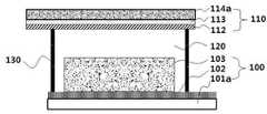
이러한 본 발명의 상대전극의 제조방법은 도 1에 도시된 방법에 따라 제조되는 것이 바람직하다. 도 1은 본 발명에 따른 플렉서블 상대 전극의 제조방법과 상기 상대전극을 포함하는 염료감응 태양전지의 제조 방법을 설명하기 위한 공정의 개략도이다.Such a method of manufacturing the counter electrode of the present invention is preferably manufactured according to the method shown in FIG. 1 is a schematic diagram of a process for explaining a method of manufacturing a flexible counter electrode and a method of manufacturing a dye-sensitized solar cell including the counter electrode according to the present invention.
도 1을 참조하면, 본 발명은 고온 내성을 가지는 제1 기판(101)을 준비하고, 그 위에 탄소기반 재료와 백금 나노입자를 포함하는 다공질막 형성용 페이스트를 코팅한 후 고온 소성으로 탄소기반 재료와 백금 나노입자를 포함하는 촉매 역할을 하는 다공질막(112)을 형성한다(도 1의 (a)).Referring to FIG. 1, the present invention prepares a
그런 다음, 본 발명에서는 상기 다공질막(112) 위에 점착층(113) 및 제 2기판(114)을 순차적으로 적층한 후 가열 압착하여 고온 내성을 가지는 제1 기판(101), 탄소기반 재료와 백금 나노입자를 포함하는 다공질막(112), 점착층(113) 및 제 2기판(114)을 포함하는 A 기판을 제조한다(도 1의 (b)).Next, in the present invention, the pressure-sensitive
이어서, HF 용액을 이용하는 전사법으로 상기 A 기판에서 고온 내성을 가지는 제1 기판(101)을 분리하고 상기 다공질막(112) 및 점착층(113)을 제 2기판 쪽으로 이동시켜 제 2기판(114), 상기 제 2기판 위에 형성된 점착층(113) 및 다공질막(112)을 포함하는 B 기판을 제조하여 상대전극의 제조를 완성한다(도 1의 (c), (d)).Subsequently, the
상술한 방법으로 제조된 상대전극은 통상의 염료감응 태양전지로 사용될 수 있는 바, 본 발명에서는 이를 광전극과 전해질을 이용하여 염료감응 태양전지를 제공할 수 있다.The counter electrode manufactured by the above-described method may be used as a conventional dye-sensitized solar cell. In the present invention, the counter electrode may provide a dye-sensitized solar cell using the photoelectrode and the electrolyte.
따라서, 본 발명은 상기 플렉서블 상대전극에 대하여 소정의 간격을 두고 서로 마주보도록 광전극을 배치한 후, 전해질(120)을 주입하고 고분자 접착체(130)로 봉합하여 염료감응 태양전지를 제조할 수 있다(도 1의 (e)).Therefore, in the present invention, after the photoelectrodes are disposed to face each other at a predetermined interval with respect to the flexible counter electrode, the
A 기판 제조A substrate manufacturing
상기 A 기판을 제조하는 단계는, 고온 내성을 가지는 제1 기판(101)의 일면에 탄소기반 재료와 백금 나노입자를 포함하는 다공질막(112)을 형성하는 단계, 및 상기 탄소기반 재료와 백금 나노입자를 포함하는 다공질막(112) 상에 점착층(113) 및 제 2기판(114)을 차례로 적층하고 기판을 가열 압착하는 단계를 포함할 수 있다.The manufacturing of the A substrate may include forming a
본 발명은 투명 열융착 고분자 필름과 같은 점착층 및 제 2기판을 상기 다공질막 위에 적층하여 올린 후, 열과 압력을 가해 고온 내성을 가지는 제1 기판(101)-다공질막(112)-점착층(113)-제 2기판(114)의 순서로 붙어있는 A 기판을 제조한다.According to the present invention, a pressure-sensitive adhesive layer and a second substrate, such as a transparent heat-sealed polymer film, are laminated and raised on the porous membrane, and then applied to the first substrate 101-porous membrane 112-adhesive layer having high temperature resistance by applying heat and pressure ( 113)-A substrate attached in the order of the
본 발명에서 상기 다공질막은 탄소기반 재료, 백금 나노입자, 바인더 및 용매를 포함하는 페이스트를 고온 내성을 가지는 제1 기판의 일면에 코팅하고 450 내지 500℃의 온도에서 1~2시간 동안 열처리하여 형성할 수 있다.In the present invention, the porous membrane may be formed by coating a paste including a carbon-based material, platinum nanoparticles, a binder, and a solvent on one surface of a first substrate having high temperature resistance and heat-treating at a temperature of 450 to 500 ° C. for 1 to 2 hours. Can be.
또한 상기 다공질막은 전극 & 촉매층으로서 그 두께는 특별히 한정되지 않으나, 바람직하게 1 내지 100 um일 수 있다.In addition, the thickness of the porous membrane as an electrode & catalyst layer is not particularly limited, but may be preferably 1 to 100um.
상기 페이스트는 카본(탄소기반재료)과 백금 나노 입자의 중량비가 1:99 내지 99:1일 수 있으며, 보다 바람직하게 90:10 내지 95:5 일 수 있다.The paste may have a weight ratio of carbon (carbon-based material) and platinum nanoparticles of 1:99 to 99: 1, and more preferably 90:10 to 95: 5.
상기 페이스트는 이 분야에 잘 알려진 방법으로 제조될 수 있으며, 그 방법이 특별히 한정되지 않는다. 예를 들면, 상기 페이스트는 탄소기반 재료와 백금 나노입자를 용매에 혼합하여 금속산화물이 분산된 점도 5×10⁴ 내지 5×10⁵ cps의 콜로이드 용액을 제조한 후, 바인더 수지를 첨가하여 혼합하고, 증류기로 용매를 제거하여 제조할 수 있다. 또 다른 방법으로, 페이스트는 탄소기판 재료와, 바인더 및 용매를 혼합하여 1차적으로 페이스트를 제조한 후, 여기에 백금 나노 입자를 첨가하여 제조될 수 있다. 후자의 방법이 사용되는 경우, 상기 페이스트는 5 내지 30 중량%의 탄소기반 재료, 0.01 내지 10 중량%의 바인더 및 잔량의 용매를 포함하는 페이스트 100 중량부를 기준으로, 1 내지 20 중량부의 백금 나노입자를 첨가하여 제조될 수 있다.The paste may be prepared by a method well known in the art, and the method is not particularly limited. For example, the paste may be prepared by mixing a carbon-based material and platinum nanoparticles in a solvent to prepare a colloidal solution having a viscosity of 5 × 10⁴ to 5 × 10⁵ cps in which a metal oxide is dispersed, and then adding and mixing a binder resin. It can be prepared by removing the solvent with a still. Alternatively, the paste may be prepared by first mixing the carbon substrate material, a binder and a solvent to prepare a paste, and then adding platinum nanoparticles thereto. When the latter method is used, the paste may contain from 1 to 20 parts by weight of platinum nanoparticles, based on 100 parts by weight of a paste comprising 5 to 30% by weight of carbon-based material, 0.01 to 10% by weight of a binder and the balance of solvent. It can be prepared by adding.
또한 상기 탄소기반 재료와 백금 나노입자, 바인더 수지 및 용매의 혼합 비율과 종류는 특별히 한정되지는 않고, 상술한 탄소기반 재료와 백금 나노입자의 중량비를 만족하는 조건이면, 이 분야에 잘 알려진 방법으로 사용될 수 있다. 바람직하게, 상기 탄소기반 재료는 활성탄, 흑연, 카본 나노튜브, 카본블랙 및 그라펜으로 이루어진 군으로부터 1종 이상을 사용할 수 있다. 또한 상기 바인더 수지는 폴리에틸렌글리콜, 폴리에틸렌옥사이드, 폴리비닐알코올, 폴리비닐피롤리돈, 에틸셀룰로오스 등을 사용할 수 있다. 또한, 상기 용매는 에탄올, 메탄올, 터피네올, 라우르산 등을 사용할 수 있다.In addition, the mixing ratio and type of the carbon-based material and the platinum nanoparticles, the binder resin, and the solvent are not particularly limited, and as long as conditions satisfying the weight ratio of the carbon-based material and the platinum nanoparticles are well known, Can be used. Preferably, the carbon-based material may be used one or more from the group consisting of activated carbon, graphite, carbon nanotubes, carbon black and graphene. In addition, the binder resin may be polyethylene glycol, polyethylene oxide, polyvinyl alcohol, polyvinylpyrrolidone, ethyl cellulose and the like. In addition, the solvent may be ethanol, methanol, terpineol, lauric acid and the like.
상기 페이스트에서 탄소기반 재료와 백금 나노입자는 입자 크기가 각각 10nm 내지 100㎛(평균 입경)인 것이 바람직하다.In the paste, the carbon-based material and the platinum nanoparticles each preferably have a particle size of 10 nm to 100 μm (average particle diameter).
또한 상기 페이스트의 코팅을 위한 고온 내성을 가지는 제1 기판(101)으로는 고온에서 소성할 수 있는 기판이면 모두 사용 가능하고, 예를 들면 금속기판, 유리기판, 또는 세라믹 기판을 사용할 수 있고, 바람직하게 유리기판을 사용한다. 또한 상기 기판 반드시 투명할 필요는 없으므로 상기 제1 기판은 전도성 필름을 포함하지 않는다.As the
또한 상기 제 2기판은 점착층(113)이 붙을 수 있는 기판이면 모두 사용 가능하며, 예를 들면 금속기판, 유리기판, 유연 기판인 플라스틱 기판, 직물 기판, 또는 세라믹 기판이 있다. 바람직하게, 상기 제 2기판은 유연 기판인 플라스틱 기판을 사용한다. 또한 상기 제 2기판의 두께는 50 내지 500 um일 수 있으나, 이에 한정되지는 않는다.In addition, the second substrate may be used as long as the substrate to which the
상기 플라스틱 기판은 폴리에틸렌 테레프탈레이트(PET); 폴리에틸렌나프탈레이트(PEN); 폴리카보네이트(PC); 폴리프로필렌(PP); 폴리이미드(PI); 트리아세틸셀룰로오스(TAC); 폴리에테르술폰(polyethersulfone); 메틸트리에톡시실란 (MTES), 에틸트리에톡시실란 (ETES) 및 프로필트리에톡시실란 (PTES)으로 이루어진 군에서 선택된 1종 이상의 유기금속 알콕사이드의 가수분해 및 축합반응으로 형성된 3차원 망상 구조의 유기변형 실리케이트; 이들의 공중합체; 및 이들의 혼합물로 이루어진 군으로부터 1종 이상 선택될 수 있다.The plastic substrate is polyethylene terephthalate (PET); Polyethylene naphthalate (PEN); Polycarbonate (PC); Polypropylene (PP); Polyimide (PI); Triacetylcellulose (TAC); Polyethersulfone; Three-dimensional network structure formed by the hydrolysis and condensation reaction of at least one organometallic alkoxide selected from the group consisting of methyltriethoxysilane (MTES), ethyltriethoxysilane (ETES) and propyltriethoxysilane (PTES) Organomodified silicates; Copolymers thereof; And mixtures thereof.
본 발명에서 다공질막, 점착층 등을 형성하기 위한 코팅 방법은 스크린 프린팅, 스핀 코팅, 닥터블레이트 등의 통상적인 방법을 이용할 수 있으며, 그 방법이 특별히 한정되지 않는다.In the present invention, a coating method for forming a porous membrane, an adhesive layer, or the like may use a conventional method such as screen printing, spin coating, doctor bleed, and the like, and the method is not particularly limited.
또한 상기 점착층은 열융착 고분자 필름 또는 열융착 고분자 수지를 포함하는 페이스트 또는 다공질막과 제 2기판을 붙일 수 있는 접착제를 사용하여 형성할 수 있다. 또한 점참층은 투명 또는 불투명 재료를 모두 사용할 수 있다. 바람직하게, 상기 점착층은 고분자 점착층으로서 열경화성 수지, 열가소성 수지, UV 수지, 아크릴수지계(Acrylic resin), 아크릴수지 혐기성(Acrylic resin anaerobic), 아크릴수지 에멀젼(Acrylic emulsion), 아크릴 수지계 점착테이프(Acrylic pressure-sensitive adhesive tapes), α-올레핀계(α-Olefin resin), 우레탄 수지계(Polyuretheane resin), 우레탄수지 용제형(Polyurethane solvent type), 우레탄수지 에멀젼(Urethane emulsion), 폴리우레탄수지 핫멜트(Polyurethane Hot melt, TPU), 반응성 핫멜트 접착제(R-HM), 에테르계 셀룰로오스(Ethercellulose), 에틸렌-초산비닐수지 에멀젼(Ethylene-Vinylacetate copolymer emulsion), 에틸렌-초산비닐수지 핫멜트(Ethylene-Vinylacetate copolymer Hot melt), 에폭시수지계(Epoxy resin), 에폭시수지 에멀젼(Epoxy emulsion), 염화비닐수지 용제(Polyvinyl Chloride solvent type, PVC), 초산비닐수지 에멀젼(Polyvinyl acetate emulsion), 클로로프렌 고무계(Polychloroprene rubber, CR), 시아노아크리레이트계(α-Cyanoacrylate), 실리콘계(Silicone adhesives), 변성 실리콘계(Modified Silicone adhesives), 수성고분자-이소시아네이트계 접착제(Water based polymer-isocyanate), 스틸렌-부타디엔 고무 용액계(Styrene-butadiene rubber), 스틸렌-부타디엔 고무계 라텍스(Styrene-butadiene rubber latex), 니트릴 고무계(Nitrile rubber, NBR), 니트로셀룰로오스계(Nitrocellulose), 페놀수지계(Phenolic resin), 폴리아미드수지 핫멜트(Polyamide Hot melt, PA), 폴리이미드계(Polyimide), 폴리올레핀수지 핫멜트(Polyolefin Hot melt, TPO), 폴리초산비닐수지 용제계(Polyvinyl acetate solvent type, PVAc), 폴리스티렌수지 용제계(Polystyrene solvent type, PS), 폴리비닐알코올계(Polyvinylalcohol, PVA), 폴리비닐피롤리돈 수지계(Polyvinylpyrrolidone, PVP), 폴리비닐부티랄수지계(Polyvinylbutyral, PVB), 폴리벤즈이미다졸계(Polybenzimidazole, PBI), 폴리메타크릴레이트수지 용제계(Polymethylmethacrylate solvent type, PMMA), 멜라민수지계(Melamine resin), 우레아수지계(Urea resin, UF) 및 레조르시놀 수지계(Resorcinol resin)로 이루어진 군으로부터 선택된 1종 이상의 화합물을 포함할 수 있으나, 이에 한정되는 것은 아니다. 상기 열경화성 수지나 열가소성 수지로는 설린(surlyn), 바이넬(bynel) 등이 있다. 또한, 상기 점착층은 염료감응 태양전지를 만들 때 필요한 다공질막의 면적만큼 소정의 길이로 적층하여 사용할 수 있고, 그 면적과 두께가 특별히 한정되지는 않는다.
In addition, the adhesive layer may be formed using a heat-sealing polymer film or a paste containing a heat-sealing polymer resin or an adhesive capable of attaching the porous membrane and the second substrate. The occupant layer can also use both transparent and opaque materials. Preferably, the adhesive layer is a thermosetting resin, a thermoplastic resin, a UV resin, an acrylic resin, an acrylic resin anaerobic, an acrylic resin emulsion, an acrylic resin adhesive tape (Acrylic) pressure-sensitive adhesive tapes, α-Olefin resin, Polyurethane resin, Polyurethane solvent type, Urethane emulsion, Polyurethane hot melt melt, TPU), reactive hot melt adhesive (R-HM), ether cellulose (Ethercellulose), ethylene-vinyl acetate resin emulsion, ethylene-vinyl acetate resin hot melt (Ethylene-Vinylacetate copolymer hot melt), Epoxy Resin, Epoxy Resin Emulsion, Polyvinyl Chloride Solvent Type (PVC), Polyvinyl Acetate Emulsion (Polyvinyl aceta) te emulsion), polychloroprene rubber (CR), cyanoacrylate (α-Cyanoacrylate), silicone (Silicone adhesives), modified silicone adhesives, aqueous polymer-isocyanate (Water based polymer-isocyanate) ), Styrene-butadiene rubber solution, Styrene-butadiene rubber latex, Styrene-butadiene rubber latex, Nitrile rubber (NBR), Nitrocellulose, Phenolic resin Polyamide Hot Melt (PA), Polyimide (Polyimide), Polyolefin Hot Melt (TPO), Polyvinyl Acetate Solvent (PVAc), Polystyrene Resin Solvent (Polystyrene solvent type (PS), polyvinyl alcohol (Polyvinylalcohol, PVA), polyvinylpyrrolidone resin (Polyvinylpyrrolidone, PVP), polyvinyl butyral resin (Polyvinylbutyral, PVB), Polybenzimidazole (PBI), Polymethylmethacrylate solvent type (PMMA), Melamine resin, Urea resin (UF) and Resorcinol resin It may include one or more compounds selected from the group consisting of, but is not limited thereto. The thermosetting resin and the thermoplastic resin include surlyn, bynel, and the like. In addition, the pressure-sensitive adhesive layer can be used by laminating a predetermined length as much as the area of the porous membrane required to make the dye-sensitized solar cell, the area and thickness is not particularly limited.
B 기판 제조B substrate manufacturing
상기 B 기판을 제조하는 단계는, 상기 A 기판을 HF 용액에 침지하여 상기 고온 내성을 가지는 제1 기판, 탄소기반 재료와 백금 나노입자를 포함하는 다공질막, 점착층 및 제 2기판을 포함하는 A 기판으로부터 상기 제1 기판을 분리하고 다공질막 및 점착층을 유연 기판 쪽으로 전사시키는 단계를 포함할 수 있다.The manufacturing of the B substrate may include: A comprising a first substrate having a high temperature resistance by immersing the A substrate in an HF solution, a porous membrane including a carbon-based material and platinum nanoparticles, an adhesive layer, and a second substrate. Separating the first substrate from the substrate and transferring the porous membrane and the adhesive layer toward the flexible substrate.
특히, 본 발명은 상기 단계에서 HF의 특성 중 하나인 유리기판과 같은 제1 기판 표면을 녹이는 방법을 포함한 전사 방법을 이용하는 특징이 있다. 상기 전사법은 제1 기판 위에 탄소기반 재료와 백금 나노입자를 포함하는 다공질막 필름이 있는 상태에서, 이를 HF 용액에 담가두면, HF 용액이 플라스틱 기판과 같은 제 2기판이나 점착층 표면에 손상을 시키지 않으면서, 동시에 제1 기판의 표면만 녹여 탄소기반 재료와 백금 나노입자를 포함한 다공질막과 제1 기판의 붙은 부분이 떨어져 고온 내성을 가지는 제1 기판(101)과 다공질막(112)이 분리되는 방법을 포함한다.In particular, the present invention has a feature of using a transfer method including a method of melting a surface of a first substrate, such as a glass substrate, which is one of the characteristics of HF in the step. In the transfer method, when a porous membrane film including carbon-based material and platinum nanoparticles is present on a first substrate, and soaked in an HF solution, the HF solution may damage a second substrate or an adhesive layer surface such as a plastic substrate. At the same time, only the surface of the first substrate is melted, and the porous membrane including the carbon-based material and the platinum nanoparticles is separated from the adhered portion of the first substrate, thereby separating the
상기 제1 기판이 유리기판일 경우를 예를 들어 전사 방법을 보다 상세히 설명한다.For example, the transfer method will be described in detail when the first substrate is a glass substrate.
본 발명의 전사 방법은 B 기판이 HF 용액에 침지되면, 유리로 이루어진 제1 기판의 실리콘(Si)이 HF 용액의 F-와 친화력을 가져서 제1 기판이 녹게 되고, 이에 따라 제1 기판과 다공질막 사이의 접촉 계면이 떨어지게 된다. 또한 HF 용액에 의해 상기 다공질막의 일부도 녹게 되어 제1 기판과 접촉하고 있는 다공질막과 제1 기판 사이의 계면이 분리될 수 있다. 이러한 과정을 통해서, 상기 고온 내성을 가지는 제1 기판의 하부에 형성되었던 다공질막은 상기 제1 기판의 하부로부터 완전히 분리된다.In the transfer method of the present invention, when the B substrate is immersed in the HF solution, the silicon (Si) of the first substrate made of glass has affinity with the F- of the HF solution so that the first substrate is melted, and thus the first substrate and the porous The contact interface between the films is dropped. In addition, a portion of the porous membrane is also melted by the HF solution so that the interface between the porous membrane and the first substrate in contact with the first substrate may be separated. Through this process, the porous membrane formed on the lower portion of the first substrate having high temperature resistance is completely separated from the lower portion of the first substrate.
상기 HF 용액은 HF용액과 물의 부피 비율이 1:99 ~ 100:0, 바람직하게 1:99 내지 90:10일 수 있다. 즉, 상기 전사법에서, 경우에 따라서는 HF 용액만으로 이루어진 용액을 사용할 수 있다. 하지만, HF 용액의 농도가 진해지면 제1 기판과 다공질막 표면의 분리시간이 단축 되더라도, 사용상의 위험성과 보관의 문제 및 탄소기반 재료와 백금 나노입자를 포함하는 다공질막의 필름에 좋지 않은 영향을 줄 수도 있다. 따라서, 보다 바람직하게는 HF용액과 물의 부피 비율이 1:99 내지 90:10이 되도록 하는 것이 좋다. 바람직한 일례를 들면, 본 발명은 상기 A 기판을 상기 1 내지 90% 농도의 HF 용액에 1~100분 정도 담가둔다. 상기 HF 용액에 담가두면 A 기판으로부터 제1 기판은 떨어져나가고 다공질막과 점착층은 그대로 B 기판 쪽으로 이동되어, 제 2기판(114)-점착층(113)-다공질막(112)의 순으로 B 기판이 만들어진다.The HF solution may have a volume ratio of HF solution and water of 1:99 to 100: 0, preferably 1:99 to 90:10. That is, in the transfer method, in some cases, a solution composed of only an HF solution may be used. However, as the concentration of HF solution increases, the separation time of the surface of the first substrate and the porous membrane may be shortened, but it may adversely affect the risks of use and storage and the film of the porous membrane including carbon-based materials and platinum nanoparticles. It may be. Therefore, more preferably, the volume ratio of HF solution and water is 1:99 to 90:10. In one preferred embodiment, the present invention is immersed in the substrate A in the HF solution of 1 to 90% concentration for about 1 to 100 minutes. When soaked in the HF solution, the first substrate is separated from the A substrate, and the porous membrane and the adhesive layer are moved to the B substrate as it is, so that the
또한 상기 B 기판의 다공질막 위에 적층되었던 점착층은 가열 압착에 의해 다공질막에 접착되어 있어서 다공질막이 점착층으로부터 분리되는 것을 방지할 수 있다. 또한 점착층이 필름의 전면에 접착 되어 있으므로 외부 충격에도 필름의 손상을 방지할 수 있다.In addition, the adhesive layer laminated on the porous membrane of the B substrate may be adhered to the porous membrane by heat compression, thereby preventing the porous membrane from being separated from the adhesive layer. In addition, since the adhesive layer is adhered to the entire surface of the film, it is possible to prevent damage to the film under external impact.
이때, 상기 다공질막 및 점착층은 염료감응 태양전지 제조시 필요한 만큼의 부분만 분리되어 고온 내성을 가지는 제1 기판으로부터 떨어져나갈 수 있다. 따라서, 상기 분리된 다공질막은 제 2기판에 적층된 점착층의 면적만큼만 분리되고, 나머지 부분의 다공질막은 투명 상기 제1 기판 위에 그대로 남아있게 된다.In this case, the porous membrane and the adhesive layer may be separated from the first substrate having a high temperature resistance by separating only a portion necessary for manufacturing the dye-sensitized solar cell. Therefore, the separated porous membrane is separated only by the area of the adhesive layer laminated on the second substrate, and the porous membrane of the remaining portion remains on the transparent first substrate.
한편, 본 발명의 다른 구현예에 따르면, 상기 방법에 의해 제조된 제2 기판, 상기 제 2 기판의 일면에 형성된 점착층, 및 상기 점착층 위에 형성된 탄소기반 재료와 백금 나노입자를 포함하는 다공질막을 포함하며, 상기 제2 기판은 금속기판, 유리기판, 유연 기판인 플라스틱 기판, 직물 기판, 또는 세라믹 기판인 염료감응 태양전지용 상대전극이 제공된다.On the other hand, according to another embodiment of the present invention, a porous substrate comprising a second substrate prepared by the method, an adhesive layer formed on one surface of the second substrate, and a carbon-based material and platinum nanoparticles formed on the adhesive layer The second substrate includes a metal substrate, a glass substrate, a plastic substrate as a flexible substrate, a fabric substrate, or a counter electrode for a dye-sensitized solar cell, which is a ceramic substrate.
또한 상기 탄소기반 재료는 상술한 활성탄, 흑연, 카본 나노튜브, 카본블랙 및 그라펜으로 이루어진 군으로부터 1종 이상이며, 상기 점착층은 열융착 고분자 필름 또는 열융착 고분자 수지를 포함할 수 있다.In addition, the carbon-based material is at least one selected from the group consisting of activated carbon, graphite, carbon nanotubes, carbon black, and graphene, and the adhesive layer may include a heat-sealed polymer film or a heat-sealed polymer resin.
또한 본 발명에 따르면 기판에 관계없이 적용을 할 수 있지만, 바람직하게 본 발명에서는, 제2 기판인 유연 기판(114a), 상기 유연 기판의 일면에 형성된 점착층(113), 상기 점착층 위에 형성된 탄소기반 재료와 백금 나노입자를 포함하는 다공질막(112)을 포함하는 염료감응 태양전지용 플렉서블 상대전극을 제공한다.According to the present invention, the present invention can be applied regardless of the substrate. Preferably, in the present invention, the
또한, 본 발명의 바람직한 구현예에 따르면, 상술한 상대전극, 상기 상대전극과 소정의 간격을 두고 서로 마주보도록 대향 배치된 광전극, 및 상기 상대전극과 광전극 사이의 공간을 충진하는 전해질을 포함하는 염료감응 태양전지가 제공된다.In addition, according to a preferred embodiment of the present invention, the counter electrode includes a counter electrode, a photo electrode disposed to face each other at a predetermined distance from the counter electrode, and an electrolyte filling a space between the counter electrode and the photo electrode. Dye-sensitized solar cells are provided.
도 2은 본 발명의 일 구현예에 따른 염료감응 태양전지의 개략적인 단면 구조를 나타낸 것이다. 이때, 도 2는 고온 내성을 가지는 제1 기판으로 유리 기판을 사용하고, 제 2기판으로 유연 기판을 사용한 플렉서블 염료감응 태양전지로서, 단지 본 발명을 예시하기 위한 것이며, 본 발명이 여기에 한정되는 것은 아니다.Figure 2 shows a schematic cross-sectional structure of a dye-sensitized solar cell according to an embodiment of the present invention. 2 is a flexible dye-sensitized solar cell using a glass substrate as a first substrate having high temperature resistance and a flexible substrate as a second substrate, which is merely to illustrate the present invention, and the present invention is limited thereto. It is not.
도 2에 도시한 바와 같이, 본 발명의 일 구현예에 따른 염료감응 태양전지는 제2 기판인 유연 기판(114a), 점착층(113), 탄소기반 재료와 백금 나노입자를 포함하는 다공질막(112)을 포함하는 상대전극(110), 상기 상대전극(110)과 서로 마주보도록 배치된 광전극(100), 및 상기 두 전극 사이의 공간에 채워진 전해질(120) 및 이들을 봉합하는 고분자 접착제(130)를 포함한다.As shown in FIG. 2, the dye-sensitized solar cell according to the embodiment of the present invention includes a porous substrate including a
이러한 구조를 갖는 염료감응 태양전지는, 상술한 본 발명의 전사 방법에 따라 제1 기판(유리기판)에 형성되었던 다공질막을 제 2기판(유연 기판)으로 전사시킴으로써, 상기 유연 기판 상에 우수한 에너지 변환효율을 갖는 상대전극을 형성할 수 있다.The dye-sensitized solar cell having such a structure has excellent energy conversion on the flexible substrate by transferring the porous film formed on the first substrate (glass substrate) to the second substrate (flexible substrate) according to the transfer method of the present invention described above. A counter electrode having efficiency can be formed.
한편, 본 발명에서 상기 광전극(100)은 통상적인 방법으로 형성될 수 있으며, 제 3기판 및 염료흡착 다공질막을 포함할 수 있다.Meanwhile, in the present invention, the
상기 제 3기판은 금속기판, 유리기판, 플라스틱 기판, 직물 기판, 또는 세라믹 기판일 수 있다. 또한 상기 제 3기판은 투명 전도성 전극 (TCO: transparent conducting oxide))을 의미하며, 예를 들면 SnO2:F 또는 ITO일 수 있다. 하지만, 상기 전도성 필름이 상기 물질에 한정되지는 않으며 이 분야에 잘 알려진 통상의 전도성 필름이 형성될 수 있다.The third substrate may be a metal substrate, a glass substrate, a plastic substrate, a fabric substrate, or a ceramic substrate. In addition, the third substrate refers to a transparent conducting oxide (TCO), and may be, for example, SnO2 : F or ITO. However, the conductive film is not limited to the material and a conventional conductive film well known in the art may be formed.
예를 들면, 상기 제 3기판은 FTO (F-doped SnO2: SnO2:F), ITO, 평균 두께가 1 내지 1000nm인 금속전극, 금속 질화물, 금속 산화물, 탄소화합물, 또는 전도성 고분자를 포함하는 전도성 필름이 코팅될 수 있다.For example, the third substrate includes FTO (F-doped SnO2 : SnO2 : F), ITO, a metal electrode having an average thickness of 1 to 1000 nm, a metal nitride, a metal oxide, a carbon compound, or a conductive polymer. Conductive films can be coated.
따라서, 도 2에 도시된 것처럼, 상기 광전극(100)은 제 3기판(101a), 상기 제 3기판 위에 형성된 전도성 필름(102) 및 염료흡착 다공질막(103)을 포함할 수 있다.Therefore, as shown in FIG. 2, the
상기 금속 질화물은 IVB족 금속원소의 질화물, VB족 금속원소의 질화물, VIB족 금속원소의 질화물, 질화알루미늄, 질화갈륨, 질화인듐, 질화실리콘, 질화게르마늄 및 이들의 혼합물로 이루어진 군으로부터 1종 이상 선택될 수 있다.The metal nitride is at least one selected from the group consisting of nitrides of group IVB metal elements, nitrides of group VB metal elements, nitrides of group VIB metal elements, aluminum nitride, gallium nitride, indium nitride, silicon nitride, germanium nitride, and mixtures thereof. Can be selected.
상기 금속산화물 나노입자는 입자 크기가 10 내지 100㎚인 것이 바람직하다. 상기 금속산화물 나노입자는 주석(Sn)산화물, 안티몬(Sb), 나이오븀(Nb) 또는 불소 도핑된 주석(Sn)산화물, 인듐(In)산화물, 주석 도핑된 인듐(In)산화물, 아연(Zn)산화물, 알루미늄(Al), 붕소(B), 갈륨(Ga), 수소(H), 인듐(In), 이트륨(Y), 타이타늄(Ti), 실리콘(Si) 또는 주석(Sn) 도핑된 아연(Zn)산화물, 마그네슘(Mg)산화물, 캐드뮴(Cd)산화물, 마그네슘아연(MgZn)산화물, 인듐아연(InZn)산화물, 구리알루미늄(CuAl)산화물, 실버(Ag)산화물, 갈륨(Ga)산화물, 아연주석산화물(ZnSnO), 타이타늄산화물(TiO2) 및 아연인듐주석(ZIS)산화물, 니켈(Ni)산화물, 로듐(Rh)산화물, 루세늄(Ru)산화물, 이리듐(Ir)산화물, 구리(Cu)산화물, 코발트(Co)산화물, 텅스텐(W)산화물, 티타늄(Ti)산화물, 지르코늄(Zr)산화물, 스트론튬(Sr)산화물, 란타넘(La)산화물, 바나듐(V)산화물, 몰리브데넘(Mo)산화물, 나이오븀(Nb)산화물, 알루미늄(Al)산화물, 이트늄(Y)산화물, 스칸듐(Sc)산화물, 사마륨(Sm)산화물, 스트론튬타이타늄(SrTi)산화물 및 이들의 혼합물로 이루어진 군에서 선택된 1종 이상을 사용할 수 있고, 바람직하게는 티타늄산화물을 사용한다.The metal oxide nanoparticles preferably have a particle size of 10 to 100 nm. The metal oxide nanoparticles may include tin (Sn) oxide, antimony (Sb), niobium (Nb) or fluorine-doped tin (Sn) oxide, indium (In) oxide, tin-doped indium (In) oxide, zinc (Zn). Oxide, aluminum (Al), boron (B), gallium (Ga), hydrogen (H), indium (In), yttrium (Y), titanium (Ti), silicon (Si) or tin (Sn) doped zinc (Zn) oxide, magnesium (Mg) oxide, cadmium (Cd) oxide, magnesium zinc (MgZn) oxide, indium zinc (InZn) oxide, copper aluminum (CuAl) oxide, silver (Ag) oxide, gallium (Ga) oxide , Zinc tin oxide (ZnSnO), titanium oxide (TiO2 ) and zinc indium tin (ZIS) oxide, nickel (Ni) oxide, rhodium (Rh) oxide, ruthenium (Ru) oxide, iridium (Ir) oxide, copper ( Cu) oxide, cobalt (Co) oxide, tungsten (W) oxide, titanium (Ti) oxide, zirconium (Zr) oxide, strontium (Sr) oxide, lanthanum (La) oxide, vanadium (V) oxide, molybdenum (Mo) oxide, niobium (Nb) acid At least one selected from the group consisting of water, aluminum (Al) oxide, yttrium (Y) oxide, scandium (Sc) oxide, samarium (Sm) oxide, strontium titanium (SrTi) oxide, and mixtures thereof, Preferably titanium oxide is used.
상기 탄소화합물은 활성탄, 흑연, 카본 나노튜브, 카본블랙, 그라펜 또는 이들의 혼합물로 이루어진 군으로부터 1종 이상 선택될 수 있다.The carbon compound may be at least one selected from the group consisting of activated carbon, graphite, carbon nanotubes, carbon black, graphene, or mixtures thereof.
상기 전도성 고분자는 PEDOT (폴리(3,4-에틸렌디옥시티오펜))- PSS(폴리(스티렌설포네이트)), 폴리아닐린-CSA, 펜타센, 폴리아세틸렌, P3HT(폴리(3-헥실티오펜), 폴리실록산 카르바졸, 폴리아닐린, 폴리에틸렌 옥사이드, (폴리(1-메톡시-4-(0-디스퍼스레드1)-2,5-페닐렌-비닐렌), 폴리인돌, 폴리카르바졸, 폴리피리디아진, 폴리이소티아나프탈렌, 폴리페닐렌 설파이드, 폴리비닐피리딘, 폴리티오펜, 폴리플루오렌, 폴리피리딘, 폴리피롤, 폴리설퍼나이트라이드, 및 이들의 공중합체로 이루어진 군으로부터 1종 이상 선택하여 사용할 수 있다.The conductive polymer is PEDOT (poly (3,4-ethylenedioxythiophene))-PSS (poly (styrenesulfonate)), polyaniline-CSA, pentacene, polyacetylene, P3HT (poly (3-hexylthiophene), Polysiloxane carbazole, polyaniline, polyethylene oxide, (poly (1-methoxy-4- (0-dispersed1) -2,5-phenylene-vinylene), polyindole, polycarbazole, polypyridazine , Polyisothianaphthalene, polyphenylene sulfide, polyvinylpyridine, polythiophene, polyfluorene, polypyridine, polypyrrole, polysulpernitride, and copolymers thereof. .
한편 상기 염료흡착 다공질막(103)은 금속산화물 나노입자층 포함한 광전극을 이루는 부분을 형성하기 위해서, TiO2 등을 이용하여 나노입자 필름을 형성한 것을 의미한다. 이때 상기 광전극에 형성된 다공질막의 두께도 특별히 한정되지 않으나, 바람직하게 1 내지 40 um일 수 있다.On the other hand, the dye adsorption
상기 염료흡착 다공질막은 금속산화물 나노입자, 바인더 및 용매를 포함하는 페이스트와 감광성 염료를 이용하여 통상의 방법으로 형성될 수 있다.The dye adsorption porous membrane may be formed by a conventional method using a photosensitive dye and a paste containing metal oxide nanoparticles, a binder and a solvent.
예를 들면, 상기 광전극은 제 3기판 위에 금속산화물 나노입자, 바인더 및 용매를 포함하는 금속산화물 나노입자 페이스트를 일정 두께로 도포한 후, 450 내지 500 ℃의 온도에서 1 내지 2시간 동안 열처리하여 다공질막을 형성한다. 이후, 상기 다공질막 표면에 염료를 흡착하는 단계를 수행함으로써, 광전극을 제조할 수 있다.For example, the photoelectrode is coated with a metal oxide nanoparticle paste including a metal oxide nanoparticle, a binder and a solvent to a predetermined thickness on a third substrate, and then heat-treated at a temperature of 450 to 500 ° C. for 1 to 2 hours. A porous membrane is formed. Thereafter, by performing a step of adsorbing a dye on the surface of the porous membrane, a photoelectrode may be manufactured.
상기 다공질막은 주석(Sn)산화물, 안티몬(Sb), 나이오븀(Nb) 또는 불소 도핑된 주석(Sn)산화물, 인듐(In)산화물, 주석 도핑된 인듐(In)산화물, 아연(Zn)산화물, 알루미늄(Al), 붕소(B), 갈륨(Ga), 수소(H), 인듐(In), 이트륨(Y), 타이타늄(Ti), 실리콘(Si) 또는 주석(Sn) 도핑된 아연(Zn)산화물, 마그네슘(Mg)산화물, 캐드뮴(Cd)산화물, 마그네슘아연(MgZn)산화물, 인듐아연(InZn)산화물, 구리알루미늄(CuAl)산화물, 실버(Ag)산화물, 갈륨(Ga)산화물, 아연주석산화물(ZnSnO), 타이타늄산화물(TiO2) 및 아연인듐주석(ZIS)산화물, 니켈(Ni)산화물, 로듐(Rh)산화물, 루세늄(Ru)산화물, 이리듐(Ir)산화물, 구리(Cu)산화물, 코발트(Co)산화물, 텅스텐(W)산화물, 티타늄(Ti)산화물, 지르코늄(Zr)산화물, 스트론튬(Sr)산화물, 란타넘(La)산화물, 바나듐(V)산화물, 몰리브데넘(Mo)산화물, 나이오븀(Nb)산화물, 알루미늄(Al)산화물, 이트늄(Y)산화물, 스칸듐(Sc)산화물, 사마륨(Sm)산화물, 스트론튬타이타늄(SrTi)산화물 및 이들의 혼합물로 이루어진 군으로부터 1종 이상 선택되는 금속산화물 나노입자를 포함할 수 있다.The porous membrane may include tin (Sn) oxide, antimony (Sb), niobium (Nb) or fluorine-doped tin (Sn) oxide, indium (In) oxide, tin-doped indium (In) oxide, zinc (Zn) oxide, Aluminum (Al), Boron (B), Gallium (Ga), Hydrogen (H), Indium (In), Yttrium (Y), Titanium (Ti), Silicon (Si) or Tin (Sn) Doped Zinc (Zn) Oxide, magnesium (Mg) oxide, cadmium (Cd) oxide, magnesium zinc (MgZn) oxide, indium zinc (InZn) oxide, copper aluminum (CuAl) oxide, silver (Ag) oxide, gallium (Ga) oxide, zinc tin Oxide (ZnSnO), Titanium Oxide (TiO2 ) and Zinc Indium Tin (ZIS) Oxide, Nickel (Ni) Oxide, Rhodium (Rh) Oxide, Rucenium (Ru) Oxide, Iridium (Ir) Oxide, Copper (Cu) Oxide , Cobalt (Co) oxide, tungsten (W) oxide, titanium (Ti) oxide, zirconium (Zr) oxide, strontium (Sr) oxide, lanthanum (La) oxide, vanadium (V) oxide, molybdenum (Mo) Oxide, Niobium (Nb) Oxide, Alumina (Al) oxide, yttrium (Y) oxide, scandium (Sc) oxide, samarium (Sm) oxide, strontium titanium (SrTi) oxide, and metal oxide nanoparticles selected from the group consisting of a mixture thereof Can be.
또한 상기 감광성 염료는 밴드갭 (Band Gap) 이 1.55 eV 내지 3.1 eV을 가져 가시광선을 흡수할 수 있는 염료를 사용할 수 있으며, 예를 들면 금속 또는 금속 복합체를 포함하는 유-무기 복합염료, 유기 염료 또는 이들의 혼합물을 포함할 수 있다. 상기 유-무기 복합염료의 예로는 알루미늄(Al), 백금(Pt), 팔라듐(Pd), 유로퓸(Eu), 납(Pb), 이리듐(Ir), 루테늄(Ru) 및 이들의 복합체로 이루어지는 군에서 선택된 원소를 포함하는 유-무기 복합염료일 수 있다.In addition, the photosensitive dye may be a dye that can absorb visible light having a band gap of 1.55 eV to 3.1 eV. For example, an organic-inorganic complex dye or organic dye including a metal or a metal complex may be used. Or mixtures thereof. Examples of the organic-inorganic complex dyes include aluminum (Al), platinum (Pt), palladium (Pd), europium (Eu), lead (Pb), iridium (Ir), ruthenium (Ru), and a group thereof. It may be an organic-inorganic complex dye containing an element selected from.
상기 전해질(120)은 도 2에서 설명의 편의상 간단히 채워진 상태로 도시되어 있지만, 실제로는 광전극(100) 및 상대전극(110) 사이의 공간에서 다공질막(112)인 탄소기반 재료와 백금 나노입자층의 내부에 균일하게 분산될 수 있다.The
상기 전해질은 산화-환원에 의해 상대전극으로부터 전자를 받아 광전극의 염료에 전달하는 역할을 하는 산화-환원 유도체 포함하며, 통상의 염료감응 태양전지에 사용가능한 것이면 특히 한정되지 않는다. 구체적으로 산화-환원 유도체는 요오드(I)계, 브롬(Br)계, 코발트(Co)계, 황화시안(SCN-)계, 셀레늄화시안(SeCN-)계를 함유하는 전해질로 이루어진 군으로부터 1종 이상 선택되는 것이 바람직하다. 또한 상기 전해질은 폴리비닐리덴플로라이드-co-폴리헥사플루오르프로필렌, 폴리아크릴로니트릴, 폴리에틸렌옥사이드 및 폴리알킬아크릴레이트로 이루어진 군에서 선택된 하나 이상의 고분자를 함유할 수 있다. 또한, 상기 전해질은 실리카 및 TiO2 나노입자로 이루어진 군에서 선택된 하나 이상의 무기입자를 함유하는 고분자 겔 전해질일 수 있다.The electrolyte includes an oxidation-reduction derivative which serves to receive electrons from the counter electrode by oxidation-reduction and transfer them to the dye of the photoelectrode, and is not particularly limited as long as it can be used in a conventional dye-sensitized solar cell. Specifically, the redox derivative is selected from the group consisting of an electrolyte containing iodine (I), bromine (Br), cobalt (Co), cyanide sulfide (SCN-), and cyanide selenide (SeCN-). It is preferable to select more than a species. In addition, the electrolyte may contain one or more polymers selected from the group consisting of polyvinylidene fluoride-co-polyhexafluoropropylene, polyacrylonitrile, polyethylene oxide and polyalkyl acrylate. In addition, the electrolyte may be a polymer gel electrolyte containing one or more inorganic particles selected from the group consisting of silica and TiO2 nanoparticles.
또한 상기 태양전지는 상기 반도체 전극과 상대전극을 봉합하기 위한 열융착 고분자 필름 또는 페이스트인 접착제를 더욱 포함할 수 있으며, 이때 사용되는 접착제는 통상의 물질을 사용할 수 있으므로 그 종류가 특별히 한정되지는 않는다.
In addition, the solar cell may further include an adhesive which is a heat-sealed polymer film or paste for sealing the semiconductor electrode and the counter electrode, and the type of adhesive used may be a conventional material, and thus the type is not particularly limited. .
본 발명에 따르면, 유리 기판과 같은 고온 내성을 가지는 제1 기판에 고온 소성으로 형성되었던 탄소기반 재료와 백금 나노입자를 포함하는 다공질막을, HF 용액을 이용한 전사법에 의해 플라스틱 기판과 같은 제 2기판으로 이동시킴으로써, 상기 제 2기판 위에 탄소기반 재료와 백금 나노입자를 함유한 다공질막을 포함하는 상대전극을 제조할 수 있다.According to the present invention, a porous substrate including a carbon-based material and platinum nanoparticles formed by high temperature firing on a first substrate having a high temperature resistance, such as a glass substrate, is prepared by a transfer method using an HF solution. By moving to, the counter electrode including a porous membrane containing a carbon-based material and platinum nanoparticles on the second substrate can be prepared.
따라서, 본 발명은 박막에서 보다 높은 전도성을 유지하고 전해질의 이동이 원활한 다공질 형태의 상대전극을 제공할 수 있을 뿐 아니라, 기존 플라스틱 기판에서는 사용할 수 없었던 고온 소성 필름을 이용하여 보다 우수한 안정성을 가질 수 있다. 더욱이, 본 발명의 상대전극은 점착층이 필름의 전면에 접착되어 형성되어 있으므로 외부 충격에도 필름의 손상을 방지할 수 있다.Accordingly, the present invention not only can provide a porous electrode having a higher conductivity and smoother movement of the electrolyte in the thin film, but can also have better stability by using a high temperature calcined film that cannot be used in a conventional plastic substrate. have. In addition, the counter electrode of the present invention is formed by adhering the adhesive layer to the entire surface of the film, thereby preventing damage to the film even under external impact.
또한, 본 발명에서는 고가의 투명 전도성 필름을 배제할 수 있고, 진공장비가 필요없어 가격이 저렴한 고효율의 플라스틱 기판을 이용한 유연기판 염료감응 태양전지의 상대전극을 제공할 수 있다. 또한 상기 유연 기판 대신 상술한 다양한 기판의 적용이 가능하므로, 필름 손상이 없는 고효율의 태양전지의 제공이 가능하다.
In addition, in the present invention, it is possible to exclude an expensive transparent conductive film, it is possible to provide a counter electrode of a flexible substrate dye-sensitized solar cell using a low-cost, high-efficiency plastic substrate without the need for vacuum equipment. In addition, since the above-described various substrates can be applied instead of the flexible substrate, it is possible to provide a high efficiency solar cell without damaging the film.
도 1은 본 발명의 일 구현예에 따른 플렉서블 상대전극의 제조방법과 상기 상대전극을 포함하는 염료감응 태양전지의 제조 방법을 설명하기 위한 공정의 개략도이다.
도 2는 본 발명의 일 구현예에 따른 플렉서블 염료감응 태양전지의 단면도이다.
도 3은 기존의 진공장비를 이용하여 PEN/ITO 기판 위에 백금촉매를 올린 상대전극으로 이용한 염료감응 태양전지의 단면도이다.
도 4는 본 발명의 실시예1(a)과 기존 비교예 1(b)에 따른 플렉서블 상대전극의 SEM 사진이다.
도 5는 본 발명의 일 구현예에 따른 플렉서블 상대전극의 사진이다.
도 6은 본 발명의 일 구현예에 따른 상대전극을 극세사에 적용한 사진을 나타낸 것이다.
도 7은 본 발명의 실시예 1 및 비교예 1에 따른 염료감응 태양전지의 전류-전압 곡선을 비교하여 도시한 그래프이다.1 is a schematic diagram of a process for explaining a method of manufacturing a flexible counter electrode and a method of manufacturing a dye-sensitized solar cell including the counter electrode according to an embodiment of the present invention.
2 is a cross-sectional view of the flexible dye-sensitized solar cell according to the embodiment of the present invention.
3 is a cross-sectional view of a dye-sensitized solar cell using a counter electrode on which a platinum catalyst is placed on a PEN / ITO substrate using conventional vacuum equipment.
4 is a SEM photograph of the flexible counter electrode according to Example 1 (a) and Existing Comparative Example 1 (b) of the present invention.
5 is a photograph of a flexible counter electrode according to an exemplary embodiment of the present invention.
6 is a photograph showing a counter electrode applied to a microfiber according to an embodiment of the present invention.
7 is a graph illustrating comparison of current-voltage curves of dye-sensitized solar cells according to Example 1 and Comparative Example 1 of the present invention.
이하, 본 발명에 대한 실시예를 기재한다. 다만, 하기 실시예는 본 발명의 이해를 돕기 위하여 예시하는 것일 뿐, 본 발명의 권리범위가 이들 실시예에 의해 한정되는 것은 아니다.
Hereinafter, examples of the present invention will be described. However, the following examples are merely illustrated to aid the understanding of the present invention, and the scope of the present invention is not limited to these examples.
[실시예 1]Example 1
(광전극의 제조)(Production of Photoelectrode)
광전극용 기판으로서 전도성을 가지는 유리 기판(Philkington 회사, 재질: FTO, 두께 2.2cm, 8Ω/sq, 도 2의 101a 및 102를 포함하는 기판)을 준비하였다. 이어서, 산화티타늄 나노입자(평균입경: 20 nm) 18.5 중량%, 바인더용 고분자(에틸셀룰로오스) 0.05 중량%, 및 잔량의 용매(Terpineol)를 포함하는 금속산화물 나노입자 페이스트를 상기 유리 기판 위에 도포(닥터블레이드[doctor blade]법 이용)한 후, 기판을 500 ℃에서 30 분간 열처리하여 금속산화물 나노입자를 포함하는 다공질막(두께: 9㎛)을 형성시켰다.As a substrate for a photoelectrode, a conductive glass substrate (Philkington, FTO, 2.2 cm thick, 8Ω / sq, substrate including 101a and 102 in FIG. 2) was prepared. Subsequently, a metal oxide nanoparticle paste including 18.5 wt% of titanium oxide nanoparticles (average particle diameter: 20 nm), 0.05 wt% of a polymer for binder (ethylcellulose), and a residual amount of solvent (Terpineol) was applied onto the glass substrate ( After the doctor blade method was used, the substrate was heat-treated at 500 ° C. for 30 minutes to form a porous film (thickness: 9 μm) containing metal oxide nanoparticles.
이어서, 상기 기판을 감광성 염료[Ru(4,4'-dicarboxy-2,2'-bipyridine)2(NCS)2] 0.5 mM을 포함하는 에탄올 용액에 12 시간 동안 침지하여 다공질막의 표면에 감광성 염료를 흡착시켜 광전극을 제조하였다.
Subsequently, the substrate was immersed in an ethanol solution containing 0.5 mM of photosensitive dye [Ru (4,4'-dicarboxy-2,2'-bipyridine)2 (NCS)2 ] for 12 hours to provide a photosensitive dye on the surface of the porous membrane. Adsorption was performed on the photoelectrode.
(상대전극의 제조)(Manufacture of counter electrode)
상대전극용 기판으로 유리 기판(두께: 1mm)을 준비하였다. 이어서, 탄소 나노입자(평균입경 2um, 카본블랙) 18.5 중량%, 바인더용 고분자(에틸셀룰로오스) 0.05 중량%, 및 잔량의 용매(Terpineol)를 포함하는 탄소 나노입자 페이스트를 만들었다. 이 후, 50mM Pt 용액의 10 wt%를 상기 탄소 나노입자 페이스트에 넣어 2시간 정도 교반시켰다. 잘 분산된 페이스트를 상기 유리 기판 위에 도포(닥터블레이드[doctor blade]법 이용)한 후, 기판을 450 ℃에서 30 분간 열처리하여 탄소나노입자 기반 재료와 백금 나노입자 포함하는 다공질막(두께: 12㎛)을 형성시켰다. 이어서, 탄소기반 재료와 백금 나노입자를 포함하는 다공질막 위에 투명 점착층(surlyn, bynel, 두께 25㎛)을 올리고, 그 위에 플라스틱 기판(재질: PEN, 두께 200㎛)을 올린 후 프레스 장비(상판/하판 : 80℃/100℃, 압력 1bar)로 기판을 10초동안 가열 압착하였다. 이러한 과정으로, 유리 기판 위에 형성된 다공질막, 투명 점착층(surlyn, bynel) 및 투명 플라스틱 기판을 붙인 후, 상기 기판을 5% HF 용액에 20초 동안 담그면, 유리 기판과 접착한 부분이 떨어져 탄소기반 재료와 백금 나노입자를 포함하는 다공질막이 점착층을 사이에 두고 플라스틱 기판에 붙게 된다.A glass substrate (thickness: 1 mm) was prepared as a counter electrode substrate. Subsequently, a carbon nanoparticle paste containing 18.5 wt% of carbon nanoparticles (
이러한 과정을 통해서, 플라스틱 기판 위에 상대 전극 및 촉매층을 포함하는 상대전극을 제조하였다.(도 2의 다공질막(112), 점착층(113), 제 2 기판(114a)로 이루어진 상대전극 110))Through this process, a counter electrode including a counter electrode and a catalyst layer was manufactured on the plastic substrate. (The
도 4는 본 발명의 실시예1(a)과 기존 비교예 1(b)에 따른 플렉서블 상대전극의 SEM 사진이다. 또한 도 5는 본 발명에 따른 플렉서블 상대전극의 사진이다. 또한 상기 상대전극은 직물이나 극세사에 적용 가능한데, 도 6은 본 발명에 따른 상대전극을 극세사에 적용하여 전도성을 띠고 있는 사진을 나타낸 것이다.
4 is a SEM photograph of the flexible counter electrode according to Example 1 (a) and Existing Comparative Example 1 (b) of the present invention. 5 is a photograph of the flexible counter electrode according to the present invention. In addition, the counter electrode can be applied to a fabric or microfiber, Figure 6 shows a photograph having a conductivity by applying the counter electrode according to the invention to the microfiber.
(전해질 주입 및 봉합)(Electrolyte injection and suture)
앞서 제조한 광전극과 상대전극 사이의 공간에 PMII(1-methyl-3-propylimidazolium iodide, 0.7M) 및 I2(0.03M)를 포함하는 아세토니트릴(acetonitrile) 전해질을 주입하고 통상의 고분자 수지로 봉합하여 도 2의 구조의 염료감응 태양전지를 제조하였다.
Inject the acetonitrile electrolyte containing PMII (1-methyl-3-propylimidazolium iodide, 0.7M) and I2 (0.03M) into the space between the photoelectrode and the counter electrode. Suture was prepared a dye-sensitized solar cell of the structure of FIG.
[비교예 1]Comparative Example 1
(광전극의 제조)(Production of Photoelectrode)
광전극용 기판으로서 전도성을 가지는 유리 기판(Philkington 회사, 재질: FTO, 두께 2.2cm, 8Ω/sq, 도 3의 101a 및 102를 포함하는 기판)을 준비하였다. 이어서, 산화티타늄 나노입자(평균입경: 20 nm) 18.5 중량%, 바인더용 고분자(에틸셀룰로오스) 0.05 중량%, 및 잔량의 용매(Terpineol)를 포함하는 금속산화물 나노입자 페이스트를 상기 유리 기판 위에 도포(닥터블레이드[doctor blade]법 이용)한 후, 기판을 500 ℃에서 30 분간 열처리하여 금속산화물 나노입자를 포함하는 다공질막(두께: 9㎛)을 형성시켰다.As a substrate for a photoelectrode, a conductive glass substrate (Philkington Company, FTO, 2.2 cm thick, 8Ω / sq, a substrate including 101a and 102 of FIG. 3) was prepared. Subsequently, a metal oxide nanoparticle paste including 18.5 wt% of titanium oxide nanoparticles (average particle diameter: 20 nm), 0.05 wt% of a polymer for binder (ethylcellulose), and a residual amount of solvent (Terpineol) was applied onto the glass substrate ( After the doctor blade method was used, the substrate was heat-treated at 500 ° C. for 30 minutes to form a porous film (thickness: 9 μm) containing metal oxide nanoparticles.
이어서, 상기 기판을 감광성 염료[Ru(4,4'-dicarboxy-2,2'-bipyridine)2(NCS)2] 0.5 mM을 포함하는 에탄올 용액에 12 시간 동안 침지하여 다공질막의 표면에 감광성 염료를 흡착시켜 광전극을 제조하였다.
Subsequently, the substrate was immersed in an ethanol solution containing 0.5 mM of photosensitive dye [Ru (4,4'-dicarboxy-2,2'-bipyridine)2 (NCS)2 ] for 12 hours to provide a photosensitive dye on the surface of the porous membrane. Adsorption was performed on the photoelectrode.
(상대전극의 제조)(Manufacture of counter electrode)
상대전극용 기판으로 전도성을 가지는 플라스틱 기판(Peccell Technologies 회사, 재질: PEN, 두께 188㎛, 5Ω/sq) 위에 Pt/Ti 합금(촉매층)이 30 nm 두께로 코팅된 필름을 사용하였다. (도 3의 촉매층(111), 102(전도성 필름, TCO), 유연 투명 기판(101)로 이루어진 상대전극 110).
As a counter electrode substrate, a film coated with a Pt / Ti alloy (catalyst layer) on a conductive plastic substrate (Peccell Technologies, Inc., PEN, thickness of 188 μm, 5Ω / sq) of 30 nm was used. (The
(전해질 주입 및 봉합)(Electrolyte injection and suture)
앞서 제조한 광전극과 상대전극 사이의 공간에 PMII(1-methyl-3-propylimidazolium iodide, 0.7M) 및 I2(0.03M)를 포함하는 아세토니트릴(acetonitrile) 전해질을 주입하고 통상의 고분자 수지로 봉합하여 도 3의 구조의 염료감응 태양전지를 제조하였다.
Inject the acetonitrile electrolyte containing PMII (1-methyl-3-propylimidazolium iodide, 0.7M) and I2 (0.03M) into the space between the photoelectrode and the counter electrode. Suture was prepared to dye-sensitized solar cell of the structure of FIG.
[실험예 1][Experimental Example 1]
실시예 1 및 비교예 1에서 제조한 각각의 염료감응 태양전지에 대하여 하기와 같은 방법으로 개방전압, 광전류밀도, 에너지 변환효율(energy conversion efficiency), 및 충진계수(fill factor)를 측정하였으며, 그 결과를 하기 표 1에 나타내었다. 또한, 도 7에는 AM 1.5G 1 Sun 조건에서 얻은 실시예 1 및 비교예 1의 태양전지의 전류-전압 곡선의 그래프를 비교하여 도시하였다.For each dye-sensitized solar cell manufactured in Example 1 and Comparative Example 1, the open voltage, photocurrent density, energy conversion efficiency, and fill factor were measured by the following method. The results are shown in Table 1 below. In addition, FIG. 7 shows a graph comparing current-voltage curves of the solar cells of Example 1 and Comparative Example 1 obtained under AM 1.5G 1 Sun conditions.
(1) 개방전압(V) 및 광전류밀도(㎃/㎠)(1) Open voltage (V) and photocurrent density (㎃ / ㎠)
: 개방전압과 광전류 밀도는 Keithley SMU2400 을 이용하여 측정하였다.Open voltage and photocurrent density were measured using a Keithley SMU2400.
(2) 에너지 변환효율(%) 및 충진계수(%)(2) Energy conversion efficiency (%) and filling factor (%)
: 에너지 변환효율의 측정은 1.5AM 100mW/cm2의 솔라 시뮬레이터(Xe 램프[1600W, YAMASHITA DENSO], AM1.5 filter, 및 Keithley SMU2400으로 구성됨)를 이용하였고, 충진계수는 앞서 얻은 변환효율 및 하기 계산식을 이용하여 계산하였다.The energy conversion efficiency was measured using a solar simulator (composed of Xe lamp [1600W, YAMASHITA DENSO], AM1.5 filter, and Keithley SMU2400) of 1.5AM 100mW / cm2. Calculated using.
[계산식][formula]

상기 계산식에서, J는 변환효율 곡선의 Y축 값이고, V는 변환효율 곡선의 X축 값이며, Jsc 및 Voc는 각 축의 절편 값이다.In the above formula, J is the Y-axis value of the conversion efficiency curve, V is the X-axis value of the conversion efficiency curve, and Jsc and Voc are intercept values of each axis.
(㎃/㎠)Jsc
(㎃ / ㎠)
(V)Voc
(V)
(%)FF
(%)
(%)efficiency
(%)
(㎠)Area
(㎠)
(㎛)TiO2 thickness
(Μm)
상기 표 1 및 도 7의 결과에 나타낸 바와 같이, 고온 소성한 카본과 백금 나노입자를 유연 기판으로 전사시켜 제조한 상대 전극을 포함하는 실시예 1의 염료감응 태양전지는, 기존 PEN/ITO 기판위에 Pt를 스퍼터링 하여 만든 전극을 사용하는 비교예 1의 염료감응 태양전지보다 면적 대비 좀 더 좋은 FF를 나타내었고, 이러한 FF에 기인하여 더 좋은 효율을 나타내는 것을 확인할 수 있었다.As shown in the results of Table 1 and FIG. 7, the dye-sensitized solar cell of Example 1 including a counter electrode prepared by transferring high-temperature calcined carbon and platinum nanoparticles to a flexible substrate is formed on an existing PEN / ITO substrate. It showed a better FF compared to the area than the dye-sensitized solar cell of Comparative Example 1 using the electrode made by sputtering Pt, it was confirmed that the better efficiency due to this FF.
따라서, 본 발명의 태양전지는 고가의 투명 전도성 필름을 배제하고 유연성을 갖는 플라스틱 기판 상에 고온 소성으로 형성된 전극이 효율이 우수하고 전도도가 높은 카본과 백금 나노입자 포함하므로, 유연성을 요구하는 다양한 전자 산업이나 전원이 필요한 분야에 활용될 수 있다.
Accordingly, the solar cell of the present invention excludes an expensive transparent conductive film and includes carbon and platinum nanoparticles having high conductivity and high conductivity, because the electrode formed by high-temperature firing on a flexible plastic substrate includes various electrons requiring flexibility. It can be used for industries or fields where power is needed.
100: 광전극
101a: 제 3기판
101: 제1 기판, 투명 유연 기판
102: 전도성 필름
103: 염료흡착 다공질막
110: 상대전극
111: 촉매층
112: 탄소 기반 재료와 백금 나노 입자를 포함하는 다공질막
113: 점착층
114, 114a: 제2 기판, 유연 기판
120: 전해질
130: 고분자 접착제층100: photo electrode
101a: third substrate
101: first substrate, transparent flexible substrate
102: conductive film
103: dye adsorption porous membrane
110: counter electrode
111: catalyst bed
112: A porous membrane containing a carbon-based material and platinum nanoparticles
113: adhesive layer
114, 114a: second substrate, flexible substrate
120: electrolyte
130: polymer adhesive layer
Claims (20)
Translated fromKorean(b) 전사법으로 상기 A 기판에서 상기 고온 내성을 가지는 제1 기판을 분리하고 상기 다공질막 및 점착층을 제 2기판으로 이동시켜, 제 2기판, 상기 제 2기판 위에 형성된 점착층 및 다공질막을 포함하는 B 기판을 제조하는 단계;를 포함하며,
상기 A 기판을 제조하는 단계는,
고온 내성을 가지는 제1 기판의 일면에 탄소기반 재료와 백금 나노입자를 포함하는 다공질막을 형성하는 단계, 및 상기 탄소기반 재료와 백금 나노입자를 포함하는 다공질막 상에 점착층 및 제 2기판을 차례로 적층하고 기판을 가열 압착하는 단계를 포함하고,
상기 다공질막은 탄소기반 재료, 백금 나노입자, 바인더 및 용매를 포함하는 페이스트를 고온 내성을 가지는 제1 기판의 일면에 코팅하고 450 내지 500℃의 온도에서 1~2시간 동안 열처리하여 형성하는 염료감응 태양전지용 상대전극의 제조방법.(A) preparing a substrate comprising a first substrate having a high temperature resistance that does not occur deformation at a temperature of less than 500 ℃, a porous film comprising a carbon-based material and platinum nanoparticles, an adhesive layer and a second substrate; And
(b) separating the first substrate having the high temperature resistance from the A substrate by the transfer method and moving the porous film and the adhesive layer to the second substrate, thereby forming the second substrate and the adhesive layer and the porous film formed on the second substrate. Manufacturing a B substrate comprising;
Manufacturing the A substrate,
Forming a porous membrane including a carbon-based material and platinum nanoparticles on one surface of the first substrate having high temperature resistance, and then attaching the adhesive layer and the second substrate on the porous membrane including the carbon-based material and platinum nanoparticles Laminating and heat pressing the substrate,
The porous membrane is a dye-sensitized embodiment formed by coating a paste including a carbon-based material, platinum nanoparticles, a binder, and a solvent on one surface of a first substrate having high temperature resistance and heat-treating at a temperature of 450 to 500 ° C. for 1 to 2 hours. Method of manufacturing a counter electrode for a battery.
상기 A 기판을 HF 용액에 침지하여 상기 제1 고온내성기판, 탄소기반 재료와 백금 나노입자를 포함하는 다공질막, 점착층 및 제 2기판을 포함하는 A 기판으로부터 제1 고온내성기판을 분리하고 다공질막 및 점착층을 유연 기판 쪽으로 전사시키는 단계를 포함하는, 염료감응 태양전지용 상대전극의 제조방법.The method of claim 1, wherein manufacturing the B substrate comprises:
The A substrate is immersed in an HF solution to separate the first high temperature resistant substrate from the A substrate including the first high temperature resistant substrate, the porous film including the carbon-based material and the platinum nanoparticles, the adhesive layer, and the second substrate. The method of manufacturing a counter electrode for a dye-sensitized solar cell comprising the step of transferring the film and the adhesive layer toward the flexible substrate.
열경화성 수지, 열가소성 수지, UV 수지, 아크릴수지계, 아크릴수지 혐기성, 아크릴수지 에멀젼, 아크릴수지계 점착테이프, α-올레핀계, 우레탄수지계, 우레탄수지 용제, 우레탄수지 에멀젼, 폴리우레탄수지 핫멜트, 반응성 핫멜트 접착제, 에테르계 셀룰로오스, 에틸렌-초산비닐수지 에멀젼, 에틸렌-초산비닐수지 핫멜트, 에폭시수지계, 에폭시수지 에멀젼, 염화비닐수지 용제, 초산비닐수지 에멀젼, 클로로프렌 고무계, 시아노아크리레이트계, 실리콘계, 변성 실리콘계, 수성고분자-이소시아네이트계 접착제, 스틸렌-부타디엔 고무 용액계, 스틸렌-부타디엔 고무계 라텍스, 니트릴 고무계, 니트로셀룰로오스계, 페놀수지계, 폴리아미드수지 핫멜트, 폴리이미드계, 폴리올레핀수지 핫멜트, 폴리초산비닐수지 용제계, 폴리스티렌수지 용제계, 폴리비닐알코올계, 폴리비닐피롤리돈수지계, 폴리비닐부티랄수지계, 폴리벤즈이미다졸계, 폴리메타크릴레이트수지 용제계, 멜라민수지계, 우레아수지계 및 레조르시놀계로 이루어진 군으로부터 선택된 1종 이상의 화합물을 사용하여 형성하는, 염료감응 태양전지용 상대전극의 제조방법.The method of claim 1, wherein the adhesive layer comprises a heat-sealing polymer film or a paste or adhesive containing a heat-sealing polymer resin,
Thermosetting resin, thermoplastic resin, UV resin, acrylic resin, acrylic resin anaerobic, acrylic resin emulsion, acrylic resin adhesive tape, α-olefin, urethane resin, urethane resin solvent, urethane resin emulsion, polyurethane resin hot melt, reactive hot melt adhesive, Ether cellulose, ethylene-vinyl acetate resin emulsion, ethylene-vinyl acetate resin hot melt, epoxy resin, epoxy resin emulsion, vinyl chloride resin, vinyl acetate resin emulsion, chloroprene rubber, cyanoacrylate, silicone, modified silicone, aqueous Polymer-isocyanate adhesive, styrene-butadiene rubber solution, styrene-butadiene rubber latex, nitrile rubber, nitrocellulose, phenol resin, polyamide resin hot melt, polyimide, polyolefin resin hot melt, polyvinyl acetate resin solvent, polystyrene Resin solvent type, polyvinyl alcohol Using at least one compound selected from the group consisting of all-based, polyvinylpyrrolidone resins, polyvinyl butyral resins, polybenzimidazoles, polymethacrylate resins, melamine resins, urea resins and resorcinols Forming, The manufacturing method of the counter electrode for dye-sensitized solar cells.
상기 고온 내성을 가지는 제1 기판은 금속기판, 유리기판, 또는 세라믹 기판을 사용하며,
상기 제 2기판은 금속기판, 유리기판, 유연 기판인 플라스틱 기판, 직물 기판, 또는 세라믹 기판
을 사용하는, 염료감응 태양전지용 상대전극의 제조방법.The method of claim 1,
The first substrate having high temperature resistance may use a metal substrate, a glass substrate, or a ceramic substrate.
The second substrate may be a metal substrate, a glass substrate, a flexible substrate, a plastic substrate, a fabric substrate, or a ceramic substrate.
Method for producing a counter electrode for a dye-sensitized solar cell using.
폴리에틸렌 테레프탈레이트; 폴리에틸렌나프탈레이트; 폴리카보네이트; 폴리프로필렌; 폴리이미드; 트리아세틸셀룰로오스, 폴리에테르술폰, 메틸트리에톡시실란, 에틸트리에톡시실란 및 프로필트리에톡시실란으로 이루어진 군에서 선택된 1종 이상의 유기금속 알콕사이드의 가수분해 및 축합반응으로 형성된 3차원 망상 구조의 유기변형 실리케이트; 이들의 공중합체; 및 이들의 혼합물로 이루어진 군으로부터 선택되는 1종 이상의 플라스틱 기판을 사용하는, 염료감응 태양전지용 상대전극의 제조방법.The method of claim 9, wherein the second substrate
Polyethylene terephthalate; Polyethylene naphthalate; Polycarbonate; Polypropylene; Polyimide; Organic three-dimensional network structure formed by the hydrolysis and condensation reaction of at least one organometallic alkoxide selected from the group consisting of triacetyl cellulose, polyether sulfone, methyltriethoxysilane, ethyltriethoxysilane and propyltriethoxysilane Modified silicates; Copolymers thereof; And at least one plastic substrate selected from the group consisting of a mixture thereof.
제2 기판,
상기 제 2 기판의 일면에 형성된 점착층, 및
상기 점착층 위에 형성된 탄소기반 재료와 백금 나노입자를 포함하는 다공질막을 포함하며,
상기 제2 기판은 금속기판, 유리기판, 유연 기판인 플라스틱 기판, 직물 기판, 또는 세라믹 기판인 염료감응 태양전지용 상대전극.It is prepared by the method of any one of claims 1 and 4 to 10,
Second substrate,
An adhesive layer formed on one surface of the second substrate, and
It comprises a porous membrane comprising a carbon-based material and platinum nanoparticles formed on the adhesive layer,
The second substrate may be a metal substrate, a glass substrate, a flexible substrate, a plastic substrate, a fabric substrate, or a ceramic substrate.
상기 탄소기반 재료는 활성탄, 흑연, 카본나노튜브, 카본블랙 및 그라펜으로 이루어진 군으로부터 1종 이상이며,
상기 점착층은 열융착 고분자 필름 또는 열융착 고분자 수지를 포함하는, 염료감응 태양전지용 상대전극.The method of claim 11,
The carbon-based material is at least one selected from the group consisting of activated carbon, graphite, carbon nanotubes, carbon black and graphene,
The adhesive layer comprises a heat-sealed polymer film or a heat-sealed polymer resin, a dye-sensitized solar cell counter electrode.
상기 상대전극과 소정의 간격을 두고 서로 마주보도록 대향 배치된 광전극, 및
상기 상대전극과 광전극 사이의 공간을 충진하는 전해질
을 포함하는 염료감응 태양전지.The counter electrode of claim 11,
A photoelectrode disposed to face the counter electrode at a predetermined interval to face each other, and
An electrolyte filling a space between the counter electrode and the photoelectrode
Dye-sensitized solar cell comprising a.
상기 금속 질화물은 IVB족 금속원소의 질화물, VB족 금속원소의 질화물, VIB족 금속원소의 질화물, 질화알루미늄, 질화갈륨, 질화인듐, 질화실리콘, 질화게르마늄 및 이들의 혼합물로 이루어진 군으로부터 1종 이상 선택되며,
상기 금속 산화물은 주석(Sn)산화물, 안티몬(Sb), 나이오븀(Nb) 또는 불소 도핑된 주석(Sn)산화물, 인듐(In)산화물, 주석 도핑된 인듐(In)산화물, 아연(Zn)산화물, 알루미늄(Al), 붕소(B), 갈륨(Ga), 수소(H), 인듐(In), 이트륨(Y), 타이타늄(Ti), 실리콘(Si) 또는 주석(Sn) 도핑된 아연(Zn)산화물, 마그네슘(Mg)산화물, 캐드뮴(Cd)산화물, 마그네슘아연(MgZn)산화물, 인듐아연(InZn)산화물, 구리알루미늄(CuAl)산화물, 실버(Ag)산화물, 갈륨(Ga)산화물, 아연주석산화물(ZNSNO), 타이타늄산화물(TiO2) 및 아연인듐주석(ZIS)산화물, 니켈(Ni)산화물, 로듐(Rh)산화물, 루세늄(Ru)산화물, 이리듐(Ir)산화물, 구리(Cu)산화물, 코발트(Co)산화물, 텅스텐(W)산화물, 티타늄(Ti)산화물 및 이들의 혼합물로 이루어진 군으로부터 1종 이상 선택되는 것인 염료감응 태양전지.17. The method of claim 16,
The metal nitride is at least one selected from the group consisting of nitrides of group IVB metal elements, nitrides of group VB metal elements, nitrides of group VIB metal elements, aluminum nitride, gallium nitride, indium nitride, silicon nitride, germanium nitride, and mixtures thereof. Selected,
The metal oxide may be tin (Sn) oxide, antimony (Sb), niobium (Nb) or fluorine-doped tin (Sn) oxide, indium (In) oxide, tin-doped indium (In) oxide, zinc (Zn) oxide , Aluminum (Al), boron (B), gallium (Ga), hydrogen (H), indium (In), yttrium (Y), titanium (Ti), silicon (Si) or tin (Sn) doped zinc (Zn) ) Oxide, Magnesium (Mg) Oxide, Cadmium (Cd) Oxide, Magnesium Zinc (MgZn) Oxide, Indium Zinc (InZn) Oxide, Copper Aluminum (CuAl) Oxide, Silver (Ag) Oxide, Gallium (Ga) Oxide, Zinc Tin oxide (ZNSNO), titanium oxide (TiO2 ) and zinc indium tin (ZIS) oxide, nickel (Ni) oxide, rhodium (Rh) oxide, ruthenium (Ru) oxide, iridium (Ir) oxide, copper (Cu) Dye-sensitized solar cell selected from the group consisting of oxides, cobalt (Co) oxide, tungsten (W) oxide, titanium (Ti) oxide and mixtures thereof.
Priority Applications (2)
| Application Number | Priority Date | Filing Date | Title |
|---|---|---|---|
| KR1020110122385AKR101273567B1 (en) | 2011-11-22 | 2011-11-22 | A counter electrodes for dye-sensitized solar cells and preparation method thereof |
| US13/345,415US9005457B2 (en) | 2011-11-22 | 2012-01-06 | Counter electrode for dye-sensitized solar cell and preparation method thereof |
Applications Claiming Priority (1)
| Application Number | Priority Date | Filing Date | Title |
|---|---|---|---|
| KR1020110122385AKR101273567B1 (en) | 2011-11-22 | 2011-11-22 | A counter electrodes for dye-sensitized solar cells and preparation method thereof |
Publications (2)
| Publication Number | Publication Date |
|---|---|
| KR20130056663A KR20130056663A (en) | 2013-05-30 |
| KR101273567B1true KR101273567B1 (en) | 2013-06-11 |
Family
ID=48425628
Family Applications (1)
| Application Number | Title | Priority Date | Filing Date |
|---|---|---|---|
| KR1020110122385AExpired - Fee RelatedKR101273567B1 (en) | 2011-11-22 | 2011-11-22 | A counter electrodes for dye-sensitized solar cells and preparation method thereof |
Country Status (2)
| Country | Link |
|---|---|
| US (1) | US9005457B2 (en) |
| KR (1) | KR101273567B1 (en) |
Cited By (2)
| Publication number | Priority date | Publication date | Assignee | Title |
|---|---|---|---|---|
| KR20180038088A (en) | 2016-10-05 | 2018-04-16 | 한국생산기술연구원 | Dye-sensitized solar cell comprising conducting adhesive film and PU-coated textile |
| KR20210089805A (en) | 2020-01-08 | 2021-07-19 | 동국대학교 산학협력단 | Platinum paste composition having high transmittance, preparation method of counter electrode using the same and sensitized solar cell comprising the counter electrode prepared thereby |
Families Citing this family (40)
| Publication number | Priority date | Publication date | Assignee | Title |
|---|---|---|---|---|
| US8945219B1 (en) | 2007-05-11 | 2015-02-03 | SDCmaterials, Inc. | System for and method of introducing additives to biological materials using supercritical fluids |
| US8481449B1 (en) | 2007-10-15 | 2013-07-09 | SDCmaterials, Inc. | Method and system for forming plug and play oxide catalysts |
| US9149797B2 (en) | 2009-12-15 | 2015-10-06 | SDCmaterials, Inc. | Catalyst production method and system |
| US8652992B2 (en) | 2009-12-15 | 2014-02-18 | SDCmaterials, Inc. | Pinning and affixing nano-active material |
| US9126191B2 (en) | 2009-12-15 | 2015-09-08 | SDCmaterials, Inc. | Advanced catalysts for automotive applications |
| US9039916B1 (en) | 2009-12-15 | 2015-05-26 | SDCmaterials, Inc. | In situ oxide removal, dispersal and drying for copper copper-oxide |
| US8669202B2 (en) | 2011-02-23 | 2014-03-11 | SDCmaterials, Inc. | Wet chemical and plasma methods of forming stable PtPd catalysts |
| AU2012299065B2 (en) | 2011-08-19 | 2015-06-04 | SDCmaterials, Inc. | Coated substrates for use in catalysis and catalytic converters and methods of coating substrates with washcoat compositions |
| US8715391B2 (en)* | 2012-04-10 | 2014-05-06 | Milliken & Company | High temperature filter |
| US9156025B2 (en) | 2012-11-21 | 2015-10-13 | SDCmaterials, Inc. | Three-way catalytic converter using nanoparticles |
| US9511352B2 (en) | 2012-11-21 | 2016-12-06 | SDCmaterials, Inc. | Three-way catalytic converter using nanoparticles |
| CN105592921A (en) | 2013-07-25 | 2016-05-18 | Sdc材料公司 | Washcoats and coated substrates for catalytic converters and method for manufacturing and using same |
| JP2016531725A (en)* | 2013-09-23 | 2016-10-13 | エスディーシーマテリアルズ, インコーポレイテッド | High surface area catalyst |
| CN103469555B (en)* | 2013-09-23 | 2015-04-22 | 青岛大学 | Preparation method of ultraviolet-proof antistatic graphene coating textile fabric |
| EP3060335A4 (en) | 2013-10-22 | 2017-07-19 | SDCMaterials, Inc. | Catalyst design for heavy-duty diesel combustion engines |
| WO2015061482A1 (en) | 2013-10-22 | 2015-04-30 | SDCmaterials, Inc. | Compositions of lean nox trap |
| KR101706125B1 (en)* | 2013-11-14 | 2017-02-14 | 서울대학교산학협력단 | Dye-sensitized solar cell and method for preparing the same |
| TWI480357B (en) | 2013-12-17 | 2015-04-11 | Ind Tech Res Inst | Conductive adhesive composition and electrode forming method |
| WO2015100245A1 (en)* | 2013-12-23 | 2015-07-02 | University Of Houston System | Flexible single-crystalline semiconductor device and fabrication methods thereof |
| TWI518929B (en)* | 2013-12-24 | 2016-01-21 | 財團法人工業技術研究院 | Dye-sensitized solar cell and method for fabricating the same |
| JP6326815B2 (en)* | 2013-12-27 | 2018-05-23 | 日本ゼオン株式会社 | Solar cell electrode substrate |
| CN103819842A (en)* | 2014-01-28 | 2014-05-28 | 徐松炎 | Special LED lamp forming material and manufacturing method |
| US9687811B2 (en) | 2014-03-21 | 2017-06-27 | SDCmaterials, Inc. | Compositions for passive NOx adsorption (PNA) systems and methods of making and using same |
| CN106206051B (en)* | 2016-07-01 | 2018-11-13 | 浙江工业大学 | A kind of graphene modified activated carbon and its application |
| US20180005766A1 (en)* | 2016-07-01 | 2018-01-04 | Wisconsin Alumni Research Foundation | Conductive textiles and related devices |
| CN106750116B (en)* | 2016-11-22 | 2019-03-19 | 山东科技大学 | A kind of polyurethane nano flame retardant composite material and preparation method thereof |
| CN106800777A (en)* | 2016-12-20 | 2017-06-06 | 吴中区穹窿山师匠新材料技术咨询服务部 | A kind of polyphenylene sulfide nylon graphene composite material |
| CN107393719A (en)* | 2017-05-26 | 2017-11-24 | 大连理工大学 | A method for preparing electrode materials from biomass carbon materials derived from pomelo peel |
| CN107545950B (en)* | 2017-07-19 | 2019-11-26 | 东阳市琰安建筑工程有限公司 | A kind of electric power conductive material |
| EP3473752A1 (en) | 2017-10-23 | 2019-04-24 | Fundación Imdea Materiales | Carbon nanotube-based membrane for solar cells |
| CN107866213B (en)* | 2017-11-09 | 2020-05-29 | 南京大学(苏州)高新技术研究院 | Preparation and application of powder catalytic material and phenolic resin-containing composite porous nano catalytic material |
| TWI657591B (en)* | 2017-11-29 | 2019-04-21 | 住華科技股份有限公司 | Solar optical film and manufacturing method for the same |
| TWI645973B (en)* | 2017-12-15 | 2019-01-01 | 律勝科技股份有限公司 | Polyimide thinned flexible substrate and manufacturing method thereof |
| CN109950135B (en)* | 2019-03-25 | 2021-10-08 | 深圳第三代半导体研究院 | A kind of gallium oxide nanomaterial transfer method |
| CN110182839B (en)* | 2019-05-31 | 2021-07-06 | 哈尔滨工业大学 | A method for preparing copper oxide nanoarrays using copper aluminum oxide films as precursors |
| CN113219018A (en)* | 2020-01-21 | 2021-08-06 | 王翔郁 | Non-enzymatic sensor, non-enzymatic sensing device and method for manufacturing the same |
| JP7430781B2 (en)* | 2020-12-17 | 2024-02-13 | 湖北万度光能有限責任公司 | Printable curved perovskite solar cell and its manufacturing method |
| CN112808261B (en)* | 2021-02-08 | 2022-09-02 | 长江师范学院 | Preparation method of nest-shaped niobium oxide |
| KR20220162951A (en)* | 2021-06-02 | 2022-12-09 | 주성엔지니어링(주) | Solar Cell and Method of manufacturing the same |
| CN116851007B (en)* | 2023-07-11 | 2024-09-17 | 山东交通学院 | Preparation method and magnetic field assisted photocatalysis application of carbon nanotube-indium zinc sulfide nanosheet composite material |
Citations (4)
| Publication number | Priority date | Publication date | Assignee | Title |
|---|---|---|---|---|
| KR20070059794A (en)* | 2005-12-07 | 2007-06-12 | 삼성전자주식회사 | Method for manufacturing flexible semiconductor electrode and semiconductor electrode manufactured by same, solar cell using same |
| KR20070078530A (en)* | 2006-01-27 | 2007-08-01 | 삼성전자주식회사 | Solar cell electrode, manufacturing method thereof and solar cell comprising same |
| KR20090028007A (en)* | 2007-09-13 | 2009-03-18 | 삼성전자주식회사 | Transparent electrode containing graphene sheet, display element and solar cell employing same |
| WO2011111932A2 (en) | 2010-03-09 | 2011-09-15 | Unist Academy-Industry Research Corporation | Method for manufacturing graphene, transparent electrode and active layer comprising the same, and display, electronic device, optoelectronic device, battery, solar cell, and dye-sensitized solar cell including the electrode and the active layer |
Family Cites Families (7)
| Publication number | Priority date | Publication date | Assignee | Title |
|---|---|---|---|---|
| JP4473349B2 (en)* | 1997-06-30 | 2010-06-02 | マクス−プランク−ゲゼルシャフト ツル フォルデルング デル ヴァイセンシャフト エー ファウ | Layered structure manufacturing method and semiconductor substrate |
| JP2004234988A (en)* | 2003-01-30 | 2004-08-19 | Sony Corp | Photoelectric conversion element and its manufacturing method, electronic device and its manufacturing method, and semiconductor layer and its manufacturing method |
| US20060219294A1 (en)* | 2005-03-30 | 2006-10-05 | Dai Nippon Printing Co., Ltd. | Oxide semiconductor electrode, dye-sensitized solar cell, and, method of producing the same |
| KR100722085B1 (en)* | 2005-09-12 | 2007-05-25 | 삼성전자주식회사 | Solar cell comprising carbon nanotubes formed by electrophoresis and a method of manufacturing the same |
| EP1933343A1 (en)* | 2006-12-13 | 2008-06-18 | Sony Deutschland Gmbh | A method of preparing a porous semiconductor film on a substrate |
| WO2009002876A1 (en)* | 2007-06-22 | 2008-12-31 | Washington State University Research Foundation | Hybrid structures for solar energy capture |
| TW201025702A (en)* | 2008-12-22 | 2010-07-01 | Taiwan Textile Res Inst | Dye-sensitized solar cell, cathode thereof, and method of manufacturing the same |
- 2011
- 2011-11-22KRKR1020110122385Apatent/KR101273567B1/ennot_activeExpired - Fee Related
- 2012
- 2012-01-06USUS13/345,415patent/US9005457B2/enactiveActive
Patent Citations (4)
| Publication number | Priority date | Publication date | Assignee | Title |
|---|---|---|---|---|
| KR20070059794A (en)* | 2005-12-07 | 2007-06-12 | 삼성전자주식회사 | Method for manufacturing flexible semiconductor electrode and semiconductor electrode manufactured by same, solar cell using same |
| KR20070078530A (en)* | 2006-01-27 | 2007-08-01 | 삼성전자주식회사 | Solar cell electrode, manufacturing method thereof and solar cell comprising same |
| KR20090028007A (en)* | 2007-09-13 | 2009-03-18 | 삼성전자주식회사 | Transparent electrode containing graphene sheet, display element and solar cell employing same |
| WO2011111932A2 (en) | 2010-03-09 | 2011-09-15 | Unist Academy-Industry Research Corporation | Method for manufacturing graphene, transparent electrode and active layer comprising the same, and display, electronic device, optoelectronic device, battery, solar cell, and dye-sensitized solar cell including the electrode and the active layer |
Cited By (3)
| Publication number | Priority date | Publication date | Assignee | Title |
|---|---|---|---|---|
| KR20180038088A (en) | 2016-10-05 | 2018-04-16 | 한국생산기술연구원 | Dye-sensitized solar cell comprising conducting adhesive film and PU-coated textile |
| KR20210089805A (en) | 2020-01-08 | 2021-07-19 | 동국대학교 산학협력단 | Platinum paste composition having high transmittance, preparation method of counter electrode using the same and sensitized solar cell comprising the counter electrode prepared thereby |
| KR102333686B1 (en)* | 2020-01-08 | 2021-12-01 | 동국대학교 산학협력단 | Platinum paste composition having high transmittance, preparation method of counter electrode using the same and sensitized solar cell comprising the counter electrode prepared thereby |
Also Published As
| Publication number | Publication date |
|---|---|
| US9005457B2 (en) | 2015-04-14 |
| US20130125970A1 (en) | 2013-05-23 |
| KR20130056663A (en) | 2013-05-30 |
Similar Documents
| Publication | Publication Date | Title |
|---|---|---|
| KR101273567B1 (en) | A counter electrodes for dye-sensitized solar cells and preparation method thereof | |
| KR101279586B1 (en) | Flexible electrodes and preparation method thereof, and flexible dye-sensitized solar cells using the same | |
| KR101061970B1 (en) | Photoelectrode using conductive nonmetallic film and dye-sensitized solar cell comprising same | |
| KR101437046B1 (en) | Electrodes for dye-sensitized solar cells, preparation method thereof, and solar cells using the same | |
| EP1603169B1 (en) | Photovoltaic module architecture | |
| KR101156531B1 (en) | Method for Preparing a Flexible Semiconductor Electrode, Semiconductor Electrode Prepared by the Same and Solar Cell using the Same | |
| JP5678345B2 (en) | Dye-sensitized solar cell and method for producing the same | |
| CN102084536B (en) | Method for manufacturing dye-sensitized solar cell | |
| JP2007095682A (en) | Multilayer photovoltaic device and manufacturing method thereof | |
| US10210999B2 (en) | Dye-sensitized solar cell including a semiconducting nanocomposite | |
| KR20140003998A (en) | Manufacturing technology perovskite-based mesoporous thin film solar cell | |
| KR20080006735A (en) | Solar cell using catalyst supported carbon nanotube and manufacturing method thereof | |
| KR101635758B1 (en) | Sensitizing dye solution, working electrode prepared thereby, and dye-sensitized solar cell comprising the same | |
| EP2747101A1 (en) | An opto-electronic device and method for manufacturing the same | |
| KR20190040964A (en) | Solar cell module | |
| WO2013036052A2 (en) | Photoelectrode for a dye-sensitized solar cell, method for manufacturing the photoelectrode, and dye-sensitized solar cell using the photoelectrode | |
| CN104737255A (en) | Photoelectrode for dye-sensitized solar cells, and dye-sensitized solar cell | |
| KR101627161B1 (en) | Dye-sensitized solar cell including polymer support layer, and preparing method of the same | |
| EP3473752A1 (en) | Carbon nanotube-based membrane for solar cells | |
| JP2011040288A (en) | Method of manufacturing semiconductor film, the semiconductor film, and dye-sensitized solar cell | |
| KR101369731B1 (en) | Dye-adsorption method for dye-sensitized solar cells, working electrode and dye-sensitized solar cells using the same | |
| KR102333686B1 (en) | Platinum paste composition having high transmittance, preparation method of counter electrode using the same and sensitized solar cell comprising the counter electrode prepared thereby | |
| KR20180029757A (en) | Preparation method of a counter electrode for dye-sensitized solar cell, a counter electrode fabricated thereby and dye-sensitized solar cell comprising said counter electrode | |
| KR101917425B1 (en) | Preparation method of flexible electrode, flexible electrode fabricated according to said method and flexible dye-sensitized solar cell comprising said electrode | |
| WO2014132725A1 (en) | Dye-sensitized solar cell |
Legal Events
| Date | Code | Title | Description |
|---|---|---|---|
| A201 | Request for examination | ||
| PA0109 | Patent application | St.27 status event code:A-0-1-A10-A12-nap-PA0109 | |
| PA0201 | Request for examination | St.27 status event code:A-1-2-D10-D11-exm-PA0201 | |
| P11-X000 | Amendment of application requested | St.27 status event code:A-2-2-P10-P11-nap-X000 | |
| P13-X000 | Application amended | St.27 status event code:A-2-2-P10-P13-nap-X000 | |
| D13-X000 | Search requested | St.27 status event code:A-1-2-D10-D13-srh-X000 | |
| D14-X000 | Search report completed | St.27 status event code:A-1-2-D10-D14-srh-X000 | |
| E902 | Notification of reason for refusal | ||
| PE0902 | Notice of grounds for rejection | St.27 status event code:A-1-2-D10-D21-exm-PE0902 | |
| E13-X000 | Pre-grant limitation requested | St.27 status event code:A-2-3-E10-E13-lim-X000 | |
| P11-X000 | Amendment of application requested | St.27 status event code:A-2-2-P10-P11-nap-X000 | |
| P13-X000 | Application amended | St.27 status event code:A-2-2-P10-P13-nap-X000 | |
| E701 | Decision to grant or registration of patent right | ||
| PE0701 | Decision of registration | St.27 status event code:A-1-2-D10-D22-exm-PE0701 | |
| PG1501 | Laying open of application | St.27 status event code:A-1-1-Q10-Q12-nap-PG1501 | |
| GRNT | Written decision to grant | ||
| PR0701 | Registration of establishment | St.27 status event code:A-2-4-F10-F11-exm-PR0701 | |
| PR1002 | Payment of registration fee | St.27 status event code:A-2-2-U10-U11-oth-PR1002 Fee payment year number:1 | |
| PG1601 | Publication of registration | St.27 status event code:A-4-4-Q10-Q13-nap-PG1601 | |
| P22-X000 | Classification modified | St.27 status event code:A-4-4-P10-P22-nap-X000 | |
| PN2301 | Change of applicant | St.27 status event code:A-5-5-R10-R13-asn-PN2301 St.27 status event code:A-5-5-R10-R11-asn-PN2301 | |
| FPAY | Annual fee payment | Payment date:20160601 Year of fee payment:4 | |
| PR1001 | Payment of annual fee | St.27 status event code:A-4-4-U10-U11-oth-PR1001 Fee payment year number:4 | |
| FPAY | Annual fee payment | Payment date:20170601 Year of fee payment:5 | |
| PR1001 | Payment of annual fee | St.27 status event code:A-4-4-U10-U11-oth-PR1001 Fee payment year number:5 | |
| FPAY | Annual fee payment | Payment date:20180409 Year of fee payment:6 | |
| PR1001 | Payment of annual fee | St.27 status event code:A-4-4-U10-U11-oth-PR1001 Fee payment year number:6 | |
| PC1903 | Unpaid annual fee | St.27 status event code:A-4-4-U10-U13-oth-PC1903 Not in force date:20190605 Payment event data comment text:Termination Category : DEFAULT_OF_REGISTRATION_FEE | |
| PC1903 | Unpaid annual fee | St.27 status event code:N-4-6-H10-H13-oth-PC1903 Ip right cessation event data comment text:Termination Category : DEFAULT_OF_REGISTRATION_FEE Not in force date:20190605 | |
| PN2301 | Change of applicant | St.27 status event code:A-5-5-R10-R13-asn-PN2301 St.27 status event code:A-5-5-R10-R11-asn-PN2301 | |
| P22-X000 | Classification modified | St.27 status event code:A-4-4-P10-P22-nap-X000 |