KR101271248B1 - Equipment for manufacturing semiconductor - Google Patents
Equipment for manufacturing semiconductorDownload PDFInfo
- Publication number
- KR101271248B1 KR101271248B1KR1020110077102AKR20110077102AKR101271248B1KR 101271248 B1KR101271248 B1KR 101271248B1KR 1020110077102 AKR1020110077102 AKR 1020110077102AKR 20110077102 AKR20110077102 AKR 20110077102AKR 101271248 B1KR101271248 B1KR 101271248B1
- Authority
- KR
- South Korea
- Prior art keywords
- chamber
- substrate
- cleaning
- epitaxial
- loaded
- Prior art date
- Legal status (The legal status is an assumption and is not a legal conclusion. Google has not performed a legal analysis and makes no representation as to the accuracy of the status listed.)
- Active
Links
- 238000004519manufacturing processMethods0.000titleclaimsabstractdescription18
- 239000004065semiconductorSubstances0.000titleclaimsabstractdescription16
- 239000000758substrateSubstances0.000claimsabstractdescription219
- 238000000034methodMethods0.000claimsabstractdescription118
- 238000004140cleaningMethods0.000claimsabstractdescription88
- 238000010438heat treatmentMethods0.000claimsdescription10
- KRHYYFGTRYWZRS-UHFFFAOYSA-MFluoride anionChemical compound[F-]KRHYYFGTRYWZRS-UHFFFAOYSA-M0.000claimsdescription4
- 239000007789gasSubstances0.000description52
- 238000006243chemical reactionMethods0.000description45
- 239000010408filmSubstances0.000description15
- 239000012159carrier gasSubstances0.000description10
- 239000007795chemical reaction productSubstances0.000description10
- 238000000151depositionMethods0.000description9
- 230000008021depositionEffects0.000description9
- XUIMIQQOPSSXEZ-UHFFFAOYSA-NSiliconChemical compound[Si]XUIMIQQOPSSXEZ-UHFFFAOYSA-N0.000description8
- 238000005530etchingMethods0.000description8
- 229910052710siliconInorganic materials0.000description8
- VYPSYNLAJGMNEJ-UHFFFAOYSA-NSilicium dioxideChemical compoundO=[Si]=OVYPSYNLAJGMNEJ-UHFFFAOYSA-N0.000description7
- 239000006227byproductSubstances0.000description7
- 238000000407epitaxyMethods0.000description7
- 239000013067intermediate productSubstances0.000description7
- 239000010703siliconSubstances0.000description7
- 229910052814silicon oxideInorganic materials0.000description7
- 239000012495reaction gasSubstances0.000description6
- 239000000463materialSubstances0.000description5
- 230000015572biosynthetic processEffects0.000description4
- 238000010586diagramMethods0.000description4
- 239000002019doping agentSubstances0.000description4
- 238000000197pyrolysisMethods0.000description4
- 239000000356contaminantSubstances0.000description3
- 239000001257hydrogenSubstances0.000description3
- 229910052739hydrogenInorganic materials0.000description3
- UFHFLCQGNIYNRP-UHFFFAOYSA-NHydrogenChemical compound[H][H]UFHFLCQGNIYNRP-UHFFFAOYSA-N0.000description2
- 229910017855NH 4 FInorganic materials0.000description2
- RBFQJDQYXXHULB-UHFFFAOYSA-NarsaneChemical compound[AsH3]RBFQJDQYXXHULB-UHFFFAOYSA-N0.000description2
- QVGXLLKOCUKJST-UHFFFAOYSA-Natomic oxygenChemical compound[O]QVGXLLKOCUKJST-UHFFFAOYSA-N0.000description2
- SLLGVCUQYRMELA-UHFFFAOYSA-NchlorosiliconChemical compoundCl[Si]SLLGVCUQYRMELA-UHFFFAOYSA-N0.000description2
- 238000005137deposition processMethods0.000description2
- ZOCHARZZJNPSEU-UHFFFAOYSA-NdiboronChemical compoundB#BZOCHARZZJNPSEU-UHFFFAOYSA-N0.000description2
- 239000001301oxygenSubstances0.000description2
- 229910052760oxygenInorganic materials0.000description2
- 239000013618particulate matterSubstances0.000description2
- 239000002243precursorSubstances0.000description2
- 238000007789sealingMethods0.000description2
- LIVNPJMFVYWSIS-UHFFFAOYSA-Nsilicon monoxideChemical compound[Si-]#[O+]LIVNPJMFVYWSIS-UHFFFAOYSA-N0.000description2
- 239000010409thin filmSubstances0.000description2
- YCKRFDGAMUMZLT-UHFFFAOYSA-NFluorine atomChemical compound[F]YCKRFDGAMUMZLT-UHFFFAOYSA-N0.000description1
- -1O 2Substances0.000description1
- XYFCBTPGUUZFHI-UHFFFAOYSA-NPhosphineChemical compoundPXYFCBTPGUUZFHI-UHFFFAOYSA-N0.000description1
- 229910007264Si2H6Inorganic materials0.000description1
- 229910003902SiCl 4Inorganic materials0.000description1
- 229910003910SiCl4Inorganic materials0.000description1
- 229910003818SiH2Cl2Inorganic materials0.000description1
- 229910003826SiH3ClInorganic materials0.000description1
- 229910003822SiHCl3Inorganic materials0.000description1
- 229910004298SiO 2Inorganic materials0.000description1
- BLRPTPMANUNPDV-UHFFFAOYSA-NSilaneChemical compound[SiH4]BLRPTPMANUNPDV-UHFFFAOYSA-N0.000description1
- 230000002411adverseEffects0.000description1
- 230000000903blocking effectEffects0.000description1
- 238000005229chemical vapour depositionMethods0.000description1
- 230000007797corrosionEffects0.000description1
- 238000005260corrosionMethods0.000description1
- 239000013078crystalSubstances0.000description1
- 230000007547defectEffects0.000description1
- PZPGRFITIJYNEJ-UHFFFAOYSA-NdisilaneChemical compound[SiH3][SiH3]PZPGRFITIJYNEJ-UHFFFAOYSA-N0.000description1
- 238000006073displacement reactionMethods0.000description1
- 238000001312dry etchingMethods0.000description1
- 230000003028elevating effectEffects0.000description1
- 229910052731fluorineInorganic materials0.000description1
- 239000011737fluorineSubstances0.000description1
- 229910021421monocrystalline siliconInorganic materials0.000description1
- GVGCUCJTUSOZKP-UHFFFAOYSA-Nnitrogen trifluorideChemical compoundFN(F)FGVGCUCJTUSOZKP-UHFFFAOYSA-N0.000description1
- 150000002926oxygenChemical group0.000description1
- 125000004430oxygen atomChemical groupO*0.000description1
- 238000006213oxygenation reactionMethods0.000description1
- 239000012686silicon precursorSubstances0.000description1
- FDNAPBUWERUEDA-UHFFFAOYSA-Nsilicon tetrachlorideChemical compoundCl[Si](Cl)(Cl)ClFDNAPBUWERUEDA-UHFFFAOYSA-N0.000description1
- 125000006850spacer groupChemical group0.000description1
- 239000000126substanceSubstances0.000description1
Images


Classifications
- H—ELECTRICITY
- H01—ELECTRIC ELEMENTS
- H01L—SEMICONDUCTOR DEVICES NOT COVERED BY CLASS H10
- H01L21/00—Processes or apparatus adapted for the manufacture or treatment of semiconductor or solid state devices or of parts thereof
- H01L21/02—Manufacture or treatment of semiconductor devices or of parts thereof
- H01L21/02041—Cleaning
- H01L21/02043—Cleaning before device manufacture, i.e. Begin-Of-Line process
- H01L21/02046—Dry cleaning only
- C—CHEMISTRY; METALLURGY
- C23—COATING METALLIC MATERIAL; COATING MATERIAL WITH METALLIC MATERIAL; CHEMICAL SURFACE TREATMENT; DIFFUSION TREATMENT OF METALLIC MATERIAL; COATING BY VACUUM EVAPORATION, BY SPUTTERING, BY ION IMPLANTATION OR BY CHEMICAL VAPOUR DEPOSITION, IN GENERAL; INHIBITING CORROSION OF METALLIC MATERIAL OR INCRUSTATION IN GENERAL
- C23C—COATING METALLIC MATERIAL; COATING MATERIAL WITH METALLIC MATERIAL; SURFACE TREATMENT OF METALLIC MATERIAL BY DIFFUSION INTO THE SURFACE, BY CHEMICAL CONVERSION OR SUBSTITUTION; COATING BY VACUUM EVAPORATION, BY SPUTTERING, BY ION IMPLANTATION OR BY CHEMICAL VAPOUR DEPOSITION, IN GENERAL
- C23C16/00—Chemical coating by decomposition of gaseous compounds, without leaving reaction products of surface material in the coating, i.e. chemical vapour deposition [CVD] processes
- C23C16/02—Pretreatment of the material to be coated
- C23C16/0227—Pretreatment of the material to be coated by cleaning or etching
- C23C16/0236—Pretreatment of the material to be coated by cleaning or etching by etching with a reactive gas
- C—CHEMISTRY; METALLURGY
- C23—COATING METALLIC MATERIAL; COATING MATERIAL WITH METALLIC MATERIAL; CHEMICAL SURFACE TREATMENT; DIFFUSION TREATMENT OF METALLIC MATERIAL; COATING BY VACUUM EVAPORATION, BY SPUTTERING, BY ION IMPLANTATION OR BY CHEMICAL VAPOUR DEPOSITION, IN GENERAL; INHIBITING CORROSION OF METALLIC MATERIAL OR INCRUSTATION IN GENERAL
- C23C—COATING METALLIC MATERIAL; COATING MATERIAL WITH METALLIC MATERIAL; SURFACE TREATMENT OF METALLIC MATERIAL BY DIFFUSION INTO THE SURFACE, BY CHEMICAL CONVERSION OR SUBSTITUTION; COATING BY VACUUM EVAPORATION, BY SPUTTERING, BY ION IMPLANTATION OR BY CHEMICAL VAPOUR DEPOSITION, IN GENERAL
- C23C16/00—Chemical coating by decomposition of gaseous compounds, without leaving reaction products of surface material in the coating, i.e. chemical vapour deposition [CVD] processes
- C23C16/44—Chemical coating by decomposition of gaseous compounds, without leaving reaction products of surface material in the coating, i.e. chemical vapour deposition [CVD] processes characterised by the method of coating
- C23C16/54—Apparatus specially adapted for continuous coating
- C—CHEMISTRY; METALLURGY
- C30—CRYSTAL GROWTH
- C30B—SINGLE-CRYSTAL GROWTH; UNIDIRECTIONAL SOLIDIFICATION OF EUTECTIC MATERIAL OR UNIDIRECTIONAL DEMIXING OF EUTECTOID MATERIAL; REFINING BY ZONE-MELTING OF MATERIAL; PRODUCTION OF A HOMOGENEOUS POLYCRYSTALLINE MATERIAL WITH DEFINED STRUCTURE; SINGLE CRYSTALS OR HOMOGENEOUS POLYCRYSTALLINE MATERIAL WITH DEFINED STRUCTURE; AFTER-TREATMENT OF SINGLE CRYSTALS OR A HOMOGENEOUS POLYCRYSTALLINE MATERIAL WITH DEFINED STRUCTURE; APPARATUS THEREFOR
- C30B25/00—Single-crystal growth by chemical reaction of reactive gases, e.g. chemical vapour-deposition growth
- C30B25/02—Epitaxial-layer growth
- C30B25/08—Reaction chambers; Selection of materials therefor
- C—CHEMISTRY; METALLURGY
- C30—CRYSTAL GROWTH
- C30B—SINGLE-CRYSTAL GROWTH; UNIDIRECTIONAL SOLIDIFICATION OF EUTECTIC MATERIAL OR UNIDIRECTIONAL DEMIXING OF EUTECTOID MATERIAL; REFINING BY ZONE-MELTING OF MATERIAL; PRODUCTION OF A HOMOGENEOUS POLYCRYSTALLINE MATERIAL WITH DEFINED STRUCTURE; SINGLE CRYSTALS OR HOMOGENEOUS POLYCRYSTALLINE MATERIAL WITH DEFINED STRUCTURE; AFTER-TREATMENT OF SINGLE CRYSTALS OR A HOMOGENEOUS POLYCRYSTALLINE MATERIAL WITH DEFINED STRUCTURE; APPARATUS THEREFOR
- C30B35/00—Apparatus not otherwise provided for, specially adapted for the growth, production or after-treatment of single crystals or of a homogeneous polycrystalline material with defined structure
- C30B35/005—Transport systems
- H—ELECTRICITY
- H01—ELECTRIC ELEMENTS
- H01L—SEMICONDUCTOR DEVICES NOT COVERED BY CLASS H10
- H01L21/00—Processes or apparatus adapted for the manufacture or treatment of semiconductor or solid state devices or of parts thereof
- H01L21/67—Apparatus specially adapted for handling semiconductor or electric solid state devices during manufacture or treatment thereof; Apparatus specially adapted for handling wafers during manufacture or treatment of semiconductor or electric solid state devices or components ; Apparatus not specifically provided for elsewhere
- H01L21/67005—Apparatus not specifically provided for elsewhere
- H01L21/67011—Apparatus for manufacture or treatment
- H01L21/67017—Apparatus for fluid treatment
- H01L21/67028—Apparatus for fluid treatment for cleaning followed by drying, rinsing, stripping, blasting or the like
- H01L21/6704—Apparatus for fluid treatment for cleaning followed by drying, rinsing, stripping, blasting or the like for wet cleaning or washing
- H01L21/67051—Apparatus for fluid treatment for cleaning followed by drying, rinsing, stripping, blasting or the like for wet cleaning or washing using mainly spraying means, e.g. nozzles
- H—ELECTRICITY
- H01—ELECTRIC ELEMENTS
- H01L—SEMICONDUCTOR DEVICES NOT COVERED BY CLASS H10
- H01L21/00—Processes or apparatus adapted for the manufacture or treatment of semiconductor or solid state devices or of parts thereof
- H01L21/67—Apparatus specially adapted for handling semiconductor or electric solid state devices during manufacture or treatment thereof; Apparatus specially adapted for handling wafers during manufacture or treatment of semiconductor or electric solid state devices or components ; Apparatus not specifically provided for elsewhere
- H01L21/67005—Apparatus not specifically provided for elsewhere
- H01L21/67011—Apparatus for manufacture or treatment
- H01L21/67155—Apparatus for manufacturing or treating in a plurality of work-stations
- H01L21/67161—Apparatus for manufacturing or treating in a plurality of work-stations characterized by the layout of the process chambers
- H01L21/67178—Apparatus for manufacturing or treating in a plurality of work-stations characterized by the layout of the process chambers vertical arrangement
- H—ELECTRICITY
- H01—ELECTRIC ELEMENTS
- H01L—SEMICONDUCTOR DEVICES NOT COVERED BY CLASS H10
- H01L21/00—Processes or apparatus adapted for the manufacture or treatment of semiconductor or solid state devices or of parts thereof
- H01L21/67—Apparatus specially adapted for handling semiconductor or electric solid state devices during manufacture or treatment thereof; Apparatus specially adapted for handling wafers during manufacture or treatment of semiconductor or electric solid state devices or components ; Apparatus not specifically provided for elsewhere
- H01L21/677—Apparatus specially adapted for handling semiconductor or electric solid state devices during manufacture or treatment thereof; Apparatus specially adapted for handling wafers during manufacture or treatment of semiconductor or electric solid state devices or components ; Apparatus not specifically provided for elsewhere for conveying, e.g. between different workstations
- H01L21/67739—Apparatus specially adapted for handling semiconductor or electric solid state devices during manufacture or treatment thereof; Apparatus specially adapted for handling wafers during manufacture or treatment of semiconductor or electric solid state devices or components ; Apparatus not specifically provided for elsewhere for conveying, e.g. between different workstations into and out of processing chamber
- H01L21/67757—Apparatus specially adapted for handling semiconductor or electric solid state devices during manufacture or treatment thereof; Apparatus specially adapted for handling wafers during manufacture or treatment of semiconductor or electric solid state devices or components ; Apparatus not specifically provided for elsewhere for conveying, e.g. between different workstations into and out of processing chamber vertical transfer of a batch of workpieces
Landscapes
- Engineering & Computer Science (AREA)
- Chemical & Material Sciences (AREA)
- Power Engineering (AREA)
- Physics & Mathematics (AREA)
- Microelectronics & Electronic Packaging (AREA)
- Computer Hardware Design (AREA)
- Manufacturing & Machinery (AREA)
- General Physics & Mathematics (AREA)
- Condensed Matter Physics & Semiconductors (AREA)
- Organic Chemistry (AREA)
- Metallurgy (AREA)
- Materials Engineering (AREA)
- Chemical Kinetics & Catalysis (AREA)
- General Chemical & Material Sciences (AREA)
- Crystallography & Structural Chemistry (AREA)
- Mechanical Engineering (AREA)
- Chemical Vapour Deposition (AREA)
- Drying Of Semiconductors (AREA)
- Container, Conveyance, Adherence, Positioning, Of Wafer (AREA)
- Cleaning Or Drying Semiconductors (AREA)
Abstract
Translated fromKoreanDescription
Translated fromKorean본 발명은 반도체 제조설비에 관한 것으로, 더욱 상세하게는 기판 상에 에피택셜 층을 형성하는 에피택셜 공정을 위한 반도체 제조설비에 관한 것이다.TECHNICAL FIELD The present invention relates to semiconductor manufacturing equipment, and more particularly, to a semiconductor manufacturing equipment for an epitaxial process of forming an epitaxial layer on a substrate.
통상적인 선택적 에피택시 프로세스(selective epitaxy process)는 증착 반응 및 식각 반응을 수반한다. 증착 및 식각 반응은 다결정층 및 에피택셜 층에 대해 비교적 상이한 반응 속도로 동시에 발생한다. 증착 프로세스 중에, 적어도 하나의 제2층상에, 기존의 다결정층 및/또는 비결정층이 증착되는 동안, 에피택셜 층은 단결정 표면상에 형성된다. 그러나 증착된 다결정층은 일반적으로 에피택셜 층보다 빠른 속도로 식각된다. 따라서, 부식 가스의 농도를 변화시킴으로써, 네트 선택적 프로세스(net selective process)가 에피택시 재료의 증착 및 제한된 또는 제한되지 않은 다결정 재료의 증착을 가져온다. 예를 들어, 선택적 에피택시 프로세스는, 증착물이 스페이서 상에 남아있지 않으면서 단결정 실리콘 표면상에 실리콘 함유 재료의 에피층(epilayer)의 형성을 가져올 수 있다.
Conventional selective epitaxy processes involve deposition reactions and etch reactions. The deposition and etching reactions occur simultaneously at relatively different reaction rates for the polycrystalline layer and the epitaxial layer. During the deposition process, the epitaxial layer is formed on the single crystal surface, while the existing polycrystalline and / or amorphous layer is deposited on at least one second layer. However, the deposited polycrystalline layer is generally etched at a faster rate than the epitaxial layer. Thus, by changing the concentration of the corrosive gas, a net selective process results in the deposition of epitaxial material and the deposition of limited or unlimited polycrystalline material. For example, a selective epitaxy process may result in the formation of an epilayer of silicon-containing material on a single crystal silicon surface without deposits remaining on the spacer.
선택적 에피택시 프로세스는 일반적으로 몇 가지 단점을 가진다. 이러한 에피택시 프로세스 중에 선택성을 유지시키기 위해, 전구체의 화학적 농도 및 반응 온도가 증착 프로세스에 걸쳐서 조절 및 조정되어야 한다. 충분하지 않은 실리콘 전구체가 공급되면, 식각 반응이 활성화되어 전체 프로세스가 느려진다. 또한, 기판 피처의 식각에 대해 해가 일어날 수 있다. 충분하지 않은 부식액 전구체가 공급되면, 증착 반응은 기판 표면에 걸쳐서 단결정 및 다결정 재료를 형성하는 선택성(selectivity)이 감소할 수 있다. 또한, 통상적인 선택적 에피택시 프로세스는 약 800℃, 약 1,000℃, 또는 그보다 높은 온도와 같은 높은 반응 온도를 일반적으로 요구한다. 이러한 높은 온도는 기판 표면에 대한 가능한 통제되지 않은 질화 반응 및 열 예산(thermal budge) 이유로 인해 제조 프로세스 중에 바람직하지 않다.Selective epitaxy processes generally have some disadvantages. In order to maintain selectivity during this epitaxy process, the chemical concentration of the precursor and the reaction temperature must be adjusted and adjusted throughout the deposition process. When insufficient silicon precursors are supplied, the etch reaction is activated and the whole process is slowed down. In addition, there may be a solution to the etching of the substrate features. If insufficient corrosion precursors are supplied, the deposition reaction may decrease the selectivity to form monocrystalline and polycrystalline materials across the substrate surface. In addition, typical selective epitaxy processes generally require high reaction temperatures, such as temperatures of about 800 DEG C, about 1,000 DEG C, or higher. This high temperature is undesirable during the fabrication process due to possible uncontrolled nitridation reaction to the substrate surface and thermal budget.
본 발명의 목적은 기판 상에 에피택셜 층을 형성할 수 있는 반도체 제조설비를 제공하는 데 있다.An object of the present invention is to provide a semiconductor manufacturing apparatus capable of forming an epitaxial layer on a substrate.
본 발명의 다른 목적은 기판 상에 형성된 자연산화막을 제거하고 기판 상에 자연산화막이 형성되는 것을 방지할 수 있는 반도체 제조설비를 제공하는 데 있다.Another object of the present invention is to provide a semiconductor manufacturing apparatus capable of removing a native oxide film formed on a substrate and preventing the native oxide film from being formed on the substrate.
본 발명의 또 다른 목적들은 다음의 상세한 설명과 첨부한 도면으로부터 보다 명확해질 것이다.Still other objects of the present invention will become more apparent from the following detailed description and the accompanying drawings.
본 발명의 일 실시예에 의하면, 반도체 제조설비는 기판에 대한 세정 공정이 이루어지는 세정 챔버; 상기 기판 상에 에피택셜 층을 형성하는 에피택셜 공정이 이루어지는 에피택셜 챔버; 그리고 상기 세정 챔버 및 상기 에피택셜 챔버가 측면에 연결되며, 상기 세정 공정이 완료된 상기 기판을 상기 에피택셜 챔버로 이송하는 기판 핸들러를 구비하는 이송 챔버를 포함하고, 상기 세정 챔버는 복수의 기판들에 대하여 이루어지는 배치 타입인 것을 특징으로 한다.According to an embodiment of the present invention, a semiconductor manufacturing apparatus includes a cleaning chamber in which a cleaning process is performed on a substrate; An epitaxial chamber in which an epitaxial process of forming an epitaxial layer is formed on the substrate; And a transfer chamber coupled to the side of the cleaning chamber and the epitaxial chamber and having a substrate handler for transferring the substrate having the cleaning process completed to the epitaxial chamber, wherein the cleaning chamber includes a plurality of substrates. It is characterized by the arrangement type which is made with respect to.
상기 세정 챔버는, 상기 세정 공정이 이루어지는 공정공간을 제공하는 상부챔버; 상기 기판이 출입하는 세정 통로를 가지는 하부챔버; 상기 기판이 적재되는 기판 홀더; 상기 기판 홀더에 연결되어 상기 기판 홀더와 함께 승강하며, 상기 기판 홀더를 상기 상부챔버 및 상기 하부챔버로 이동하는 회전축; 그리고 상기 기판 홀더와 함께 승강하며, 상기 세정 공정 동안 상기 공정공간을 외부로부터 차단하는 지지판을 구비할 수 있다.The cleaning chamber may include an upper chamber providing a process space in which the cleaning process is performed; A lower chamber having a cleaning passage through which the substrate enters and exits; A substrate holder on which the substrate is loaded; A rotating shaft connected to the substrate holder to move together with the substrate holder to move the substrate holder to the upper chamber and the lower chamber; And it may be provided with a support plate for lifting up and down with the substrate holder, blocking the process space from the outside during the cleaning process.
상기 세정 챔버는 상기 회전축을 승강하는 엘리베이터 및 상기 회전축을 회전시키는 구동모터를 더 구비할 수 있다.The cleaning chamber may further include an elevator for elevating the rotating shaft and a driving motor for rotating the rotating shaft.
상기 세정 챔버는, 상기 상부챔버의 일측에 설치되어 상기 공정공간을 향해 플라즈마를 공급하는 인젝터; 상기 인젝터에 연결되어 상기 인젝터에 상기 플라즈마를 공급하는 플라즈마 공급라인; 그리고 상기 플라즈마 공급라인에 연결되며, 반응가스를 여기하여 상기 플라즈마를 생성하는 플라즈마 소스를 더 구비할 수 있다.The cleaning chamber may include an injector installed at one side of the upper chamber to supply plasma toward the process space; A plasma supply line connected to the injector to supply the plasma to the injector; And a plasma source connected to the plasma supply line to excite a reaction gas to generate the plasma.
상기 반응가스는 NF3,NH3,H2,N2로 이루어진 그룹으로부터 선택된 하나 이상일 수 있다.The reaction gas may be at least one selected from the group consisting of
상기 세정 챔버는 상기 상부챔버의 일측에 설치되어 상기 공정공간을 가열하는 히터를 더 구비할 수 있다.The cleaning chamber may further include a heater installed at one side of the upper chamber to heat the process space.
상기 이송 챔버는 상기 세정 챔버를 향해 상기 기판이 출입하는 이송 통로를 가지며, 상기 반도체 제조설비는 상기 세정 챔버와 상기 이송 챔버를 격리하는 세정측 게이트 밸브를 더 포함할 수 있다.The transfer chamber may have a transfer passage through which the substrate enters and exits toward the cleaning chamber, and the semiconductor manufacturing facility may further include a cleaning side gate valve that separates the cleaning chamber from the transfer chamber.
본 발명의 일 실시예에 의하면 기판 상에 형성된 자연산화막을 제거할 수 있을 뿐만 아니라 기판 상에 자연산화막이 형성되는 것을 방지할 수 있다. 따라서, 기판 상에 효과적으로 에피택셜 층을 형성할 수 있다.According to an embodiment of the present invention, not only the natural oxide film formed on the substrate may be removed, but the natural oxide film may be prevented from being formed on the substrate. Thus, the epitaxial layer can be effectively formed on the substrate.
도 1은 본 발명의 일 실시예에 따른 반도체 제조설비를 개략적으로 나타내는 도면이다.
도 2는 본 발명의 일 실시예에 따라 처리된 기판을 나타내는 도면이다.
도 3은 본 발명의 일 실시예에 따라 에피택셜 층을 형성하는 방법을 나타내는 흐름도이다.
도 4는 도 1에 도시한 버퍼 챔버를 나타내는 도면이다.
도 5는 도 4에 도시한 기판 홀더를 나타내는 도면이다.
도 6은 도 1에 도시한 세정 챔버를 나타내는 도면이다.
도 7은 도 1에 도시한 세정 챔버의 다른 실시예를 나타내는 도면이다.
도 8은 도 1에 도시한 에피택셜 챔버를 나타내는 도면이다.
도 9는 도 1에 도시한 공급관을 나타내는 도면이다.1 is a view schematically showing a semiconductor manufacturing apparatus according to an embodiment of the present invention.
2 is a view of a substrate processed according to one embodiment of the present invention.
3 is a flow diagram illustrating a method of forming an epitaxial layer in accordance with one embodiment of the present invention.
4 is a diagram illustrating the buffer chamber illustrated in FIG. 1.
FIG. 5 is a diagram illustrating the substrate holder shown in FIG. 4. FIG.
FIG. 6 is a view showing the cleaning chamber shown in FIG. 1.
7 is a view showing another embodiment of the cleaning chamber shown in FIG. 1.
FIG. 8 is a view showing the epitaxial chamber shown in FIG. 1.
9 is a view showing a supply pipe shown in FIG. 1.
이하, 본 발명의 바람직한 실시예들을 첨부된 도 1 내지 도 9를 참고하여 더욱 상세히 설명한다. 본 발명의 실시예들은 여러 가지 형태로 변형될 수 있으며, 본 발명의 범위가 아래에서 설명하는 실시예들에 한정되는 것으로 해석되어서는 안 된다. 본 실시예들은 당해 발명이 속하는 기술분야에서 통상의 지식을 가진 자에게 본 발명을 더욱 상세하게 설명하기 위해서 제공되는 것이다. 따라서 도면에 나타난 각 요소의 형상은 보다 분명한 설명을 강조하기 위하여 과장될 수 있다.
Hereinafter, preferred embodiments of the present invention will be described in more detail with reference to FIGS. 1 to 9. The embodiments of the present invention can be modified in various forms, and the scope of the present invention should not be construed as being limited to the embodiments described below. The embodiments are provided to explain the present invention to a person having ordinary skill in the art to which the present invention belongs. Accordingly, the shape of each element shown in the drawings may be exaggerated to emphasize a clearer description.
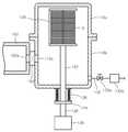
도 1은 본 발명의 일 실시예에 따른 반도체 제조설비(1)를 개략적으로 나타내는 도면이다. 반도체 제조장치(1)는 공정설비(2), 설비 전방 단부 모듈(Equipment Front End Module:EFEM)(3), 그리고 경계벽(interface wall)(4)을 포함한다. 설비 전방 단부 모듈(3)은 공정설비(2)의 전방에 장착되어, 기판들(S)이 수용된 용기(도시안됨)와 공정설비(2) 간에 웨이퍼(W)를 이송한다.
1 is a schematic view showing a
설비 전방 단부 모듈(3)은 복수의 로드포트들(loadports)(60)과 프레임(frame)(50)을 가진다. 프레임(50)은 로드포트(60)와 공정 설비(2) 사이에 위치한다. 기판(S)를 수용하는 용기는 오버헤드 트랜스퍼(overhead transfer), 오버헤드 컨베이어(overhead conveyor), 또는 자동 안내 차량(automatic guided vehicle)과 같은 이송 수단(도시안됨)에 의해 로드포트(60) 상에 놓여진다.
The plant
용기는 전면 개방 일체식 포드(Front Open Unified Pod:FOUP)와 같은 밀폐용 용기가 사용될 수 있다. 프레임(50) 내에는 로드포트(60)에 놓여진 용기와 공정설비(2) 간에 기판(S)을 이송하는 프레임 로봇(70)이 설치된다. 프레임(50) 내에는 용기의 도어를 자동으로 개폐하는 도어 오프너(도시안됨)가 설치될 수 있다. 또한, 프레임(50)에는 청정 공기가 프레임(50) 내 상부에서 하부로 흐르도록 청정 공기를 프레임(50) 내로 공급하는 팬필터 유닛(Fan Filter Unit:FFU)(도시안됨)이 제공될 수 있다.
The container may be a hermetically sealed container such as a front open unified pod (FOUP). A
기판(S)은 공정설비(2) 내에서 소정의 공정이 수행된다. 공정설비(2)는 이송 챔버(transfer chamber)(102), 로드록 챔버(loadlock chamber)(106), 세정 챔버(cleaning chamber)(108a,108b), 버퍼 챔버(buffer chamber)(110), 그리고 에피택셜 챔버(epitaxial chamber)(112a,112b,112c)를 포함한다. 이송 챔버(102)는 상부에서 바라볼 때 대체로 다각의 형상을 가지며, 로드록 챔버(106), 세정 챔버(108a,108b), 버퍼 챔버(110), 그리고 에피택셜 챔버(112a,112b,112c)는 이송 챔버(102)의 측면에 설치된다.
The substrate S is subjected to a predetermined process in the process facility 2. The process facility 2 includes a
로드록 챔버(106)는 이송 챔버(102)의 측부들 중 설비 전방 단부 모듈(3)과 인접한 측부에 위치한다. 기판(S)은 로드록 챔버(106) 내에 일시적으로 머무른 후 공정설비(2)에 로딩되어 공정이 이루어지며, 공정이 완료된 후 기판(S)은 공정설비(2)로부터 언로딩되어 로드록 챔버(106) 내에 일시적으로 머무른다. 이송 챔버(102), 세정 챔버(108a,108b), 버퍼 챔버(110), 그리고 에피택셜 챔버(112a,112b,112c)는 진공으로 유지되며, 로드록 챔버(106)는 진공 및 대기압으로 전환된다. 로드록 챔버(106)는 외부 오염물질이 이송 챔버(102), 세정 챔버(108a,108b), 버퍼 챔버(110), 그리고 에피택셜 챔버(112a,112b,112c)로 유입되는 것을 방지한다. 또한, 기판(S)의 이송 동안, 기판(S)이 대기에 노출되지 않으므로, 기판(S) 상에 산화막이 성장하는 것을 방지할 수 있다.
The
로드록 챔버(106)와 이송 챔버(102) 사이, 그리고 로드록 챔버(106)와 설비 전방 단부 모듈(3) 사이에는 게이트 밸브(도시안됨)가 설치된다. 설비 전방 단부 모듈(3)과 로드록 챔버(106) 간에 기판(S)이 이동하는 경우, 로드록 챔버(106)와 이송 챔버(102) 사이에 제공된 게이트 밸브가 닫히고, 로드록 챔버(106)와 이송 챔버(102) 간에 기판(S)이 이동하는 경우, 로드록 챔버(106)와 설비 전방 단부 모듈(3) 사이에 제공되는 게이트 밸브가 닫힌다.
A gate valve (not shown) is installed between the
이송 챔버(102)는 기판 핸들러(104)를 구비한다. 기판 핸들러(104)는 로드록 챔버(106), 세정 챔버(108a,108b), 버퍼 챔버(110), 그리고 에피택셜 챔버(112a,112b,112c) 사이에서 기판(S)을 이송한다. 이송 챔버(102)는 기판(S)이 이동할 때 진공을 유지하도록 밀봉된다. 진공을 유지하는 것은 기판(S)이 오염물(예를 들면, O2, 입자상 물질 등)에 노출되는 것을 방지하기 위함이다.
The
에피택셜 챔버(112a,112b,112c)는 기판(S) 상에 에피택셜 층을 형성하기 위하여 제공된다. 본 실시예에서는 3개의 에피택셜 챔버(112a,112b,112c)가 제공된다. 에피택셜 공정은 세정 공정에 비해 많은 시간이 소요되므로, 복수의 에피택셜 챔버를 통해 제조수율을 향상시킬 수 있다. 본 실시예와 달리, 4개 이상이나 2개 이하의 에피택셜 챔버가 제공될 수 있다.
The
세정 챔버(108a,108b)는 에피택셜 챔버(112a,112b,112c) 내에서 기판(S)에 대한 에피택셜 공정이 이루어지기 이전에 기판(S)을 세정하기 위하여 제공된다. 에피택셜 공정이 성공적으로 이루어지기 위해서는 결정성 기판 상에 존재하는 산화물의 양이 최소화되어야 한다. 기판의 표면 산소 함유량이 너무 높은 경우, 산소 원자가 시드 기판 상의 증착재료의 결정학적 배치를 방해하기 때문에, 에피택셜 공정은 유해한 영향을 받는다. 예를 들면, 실리콘 에피택셜 증착시, 결정성 기판 상의 과도한 산소는, 원자 단위의 산소 원자 클러스터에 의해, 실리콘 원자를 그 에피택셜 위치로부터 변위되게 할 수 있다. 이러한 국소적인 원자 변위는 층이 더 두껍게 성장할 때 후속 원자 배열에 오차를 일으킬 수 있다. 이러한 현상은 이른바 적층 결함 또는 힐락(hillock defects)으로 지칭될 수 있다. 기판 표면의 산소화(oxygenatoin)는, 예를 들면 기판이 이송할 때 대기에 노출되는 경우 발생할 수 있다. 따라서, 기판(S) 상에 형성된 자연 산화막(native oxide)(또는 표면 산화물)을 제거하는 세정 공정이 세정 챔버(108a,108b) 내에서 이루어질 수 있다.
The
세정 공정은 라디칼 상태의 수소(H*)와 NF3 가스를 사용하는 건식 에칭 공정이다. 예를 들어, 기판의 표면에 형성된 실리콘 산화막을 에칭하는 경우, 챔버 내에 기판을 배치하고 챔버 내에 진공 분위기를 형성한 후, 챔버 내에서 실리콘 산화막과 반응하는 중간 생성물을 발생시킨다.
The cleaning process is a dry etching process using radical hydrogen (H* ) and NF3 gas. For example, when the silicon oxide film formed on the surface of the substrate is etched, a substrate is placed in the chamber and a vacuum atmosphere is formed in the chamber, and then an intermediate product reacting with the silicon oxide film in the chamber is generated.
예를 들어, 챔버 내에 수소 가스의 라디칼(H*)과 불화물 가스(예를 들어, 불화질소(NF3))와 같은 반응성 가스를 공급하면, 아래 반응식(1)과 같이 반응성 가스가 환원되어 NHxFy(x,y는 임의의 정수)와 같은 중간 생성물이 생성된다.
For example, when a reactive gas such as a radical H* of a hydrogen gas and a fluoride gas (for example, nitrogen fluoride (NF3 )) is supplied into the chamber, the reactive gas is reduced as shown in the following reaction formula (1)x Fy (where x and y are arbitrary integers).

중간 생성물은 실리콘 산화막(SiO2)과 반응성이 높기 때문에, 중간 생성물이 실리콘 기판의 표면에 도달하면 실리콘 산화막과 선택적으로 반응하여 아래 반응식(2)와 같이 반응 생성물((NH4)2SiF6)이 생성된다.Since the intermediate product is highly reactive with the silicon oxide film (SiO2 ), when the intermediate product reaches the surface of the silicon substrate, the reaction product ((NH4 )2 SiF6 ) selectively reacts with the silicon oxide film, Is generated.

이후, 실리콘 기판을 100℃ 이상으로 가열하면 아래 반응식(3)과 같이 반응 생성물이 열분해하여 열분해 가스가 되어 증발되므로, 결과적으로 기판 표면으로부터 실리콘 산화막이 제거될 수 있다. 아래 반응식(3)과 같이, 열분해 가스는 HF 가스나 SiF4 가스와 같이 불소를 함유하는 가스가 포함된다.
Thereafter, when the silicon substrate is heated to 100 ° C or higher, the reaction product is pyrolyzed as a pyrolysis gas and evaporated as shown in the following reaction formula (3). As a result, the silicon oxide film can be removed from the surface of the substrate. As shown in the following reaction formula (3), pyrolysis gas includes fluorine-containing gas such as HF gas or SiF4 gas.

위와 같이, 세정 공정은 반응 생성물을 생성하는 반응 공정 및 반응 생성물을 열분해하는 히팅 공정을 포함하며, 반응 공정 및 히팅 공정은 세정 챔버(108a,108b) 내에서 함께 이루어지거나, 세정 챔버(108a,108b) 중 어느 하나에서 반응 공정이 이루어지고 세정 챔버(108a,108b) 중 다른 하나에서 히팅 공정이 이루어질 수 있다.
As described above, the cleaning process includes a reaction process for producing a reaction product and a heating process for pyrolyzing the reaction product, and the reaction process and the heating process are performed together in the
버퍼 챔버(110)는 세정 공정이 완료된 기판(S)이 적재되는 공간과 에피택셜 공정이 이루어진 기판(S)이 적재되는 공간을 제공한다. 세정 공정이 완료되면, 기판(S)은 에피택셜 챔버(112a,112b,112c)로 이송되기 이전에 버퍼 챔버(110)로 이동하여 버퍼 챔버(110) 내에 적재된다. 에피택셜 챔버(112a,112b,112c)는 복수의 기판들에 대한 단일 공정이 이루어지는 배치 타입(batch type)일 수 있으며, 에피택셜 챔버(112a,112b,112c) 내에서 에피택셜 공정이 완료되면, 에피택셜 공정이 이루어진 기판(S)은 버퍼 챔버(110) 내에 순차적으로 적재되고, 세정 공정이 완료된 기판(S)은 에피택셜 챔버(112a,112b,112c) 내에 순차적으로 적재된다. 이때, 기판(S)은 버퍼 챔버(110) 내에 종방향으로 적재될 수 있다.
The
도 2는 본 발명의 일 실시예에 따라 처리된 기판을 나타내는 도면이다. 앞서 설명한 바와 같이, 기판(S)에 대한 에피택셜 공정이 이루어지기 이전에 기판(S)에 대한 세정 공정이 세정 챔버(108a,108b) 내에서 이루어지며, 세정 공정을 통해 기판(70)의 표면에 형성된 산화막(72)을 제거할 수 있다. 산화막은 세정 챔버(108a,108b) 내에서 세정 공정을 통해 제거될 수 있다. 세정 공정을 통해 기판(70)의 표면 상에 에피택시 표면(74)이 노출될 수 있으며, 이를 통해 에피택셜 층의 성장을 돕는다.
2 is a view of a substrate processed according to one embodiment of the present invention. As described above, a cleaning process for the substrate S is performed in the
이후, 기판(S) 상에 에피택셜 공정이 에피택셜 챔버(112a,112b,112c) 내에서 이루어진다. 에피택셜 공정은 화학기상증착에 의해 이루어질 수 있으며, 에피택시 표면(74) 상에 에피택시 층(76)을 형성할 수 있다. 기판(70)의 에피택시 표면(74)은 실리콘 가스(예를 들어, SiCl4, SiHCl3, SiH2Cl2, SiH3Cl, Si2H6, 또는 SiH4) 및 캐리어 가스(예를 들어, N2 및/또는 H2)를 포함하는 반응가스에 노출될 수 있다. 또한, 에피택시 층(76)이 도펀트를 포함할 것이 요구되는 경우, 실리콘 함유 가스는 도펀트 함유 가스(예를 들면, 아르신(AsH3), 포스핀(PH3), 및/또는 디보란(B2H6))를 포함할 수 있다.
Subsequently, an epitaxial process is performed on the substrate S in the
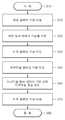
도 3은 본 발명의 일 실시예에 따라 에피택셜 층을 형성하는 방법을 나타내는 흐름도이다. 방법은 단계(S10)로부터 시작한다. 단계(S20)에서, 기판(S)은 에피택셜 공정 전에 세정 챔버(108a,108b)로 이동하며, 기판 핸들러(104)는 기판(S)을 세정 챔버(108a,108b)로 이송한다. 이송은 진공으로 유지되는 이송 챔버(102)를 통해 이루어진다. 단계(S30)에서, 기판(S)에 대한 세정 공정이 이루어진다. 앞서 설명한 바와 같이, 세정 공정은 반응 생성물을 생성하는 반응 공정 및 반응 생성물을 열분해하는 히팅 공정을 포함한다. 반응 공정 및 히팅 공정은 세정 챔버(108a,108b) 내에서 함께 이루어지거나, 세정 챔버(108a,108b) 중 어느 하나에서 반응 공정이 이루어지고 세정 챔버(108a,108b) 중 다른 하나에서 히팅 공정이 이루어질 수 있다.
3 is a flow diagram illustrating a method of forming an epitaxial layer in accordance with one embodiment of the present invention. The method starts from step S10. In step S20, the substrate S is moved to the
단계(S40)에서, 세정 공정이 완료된 기판(S)은 버퍼 챔버(110)로 이송되어 버퍼 챔버(110) 내에 적재되며, 버퍼 챔버(110) 내에서 에피택셜 공정을 대기한다. 단계(S50)에서 기판(S)은 에피택셜 챔버(112a,112b,112c)로 이송되며, 이송은 진공으로 유지되는 이송 챔버(102)를 통해 이루어진다. 단계(S60)에서 기판(S) 상에 에피택셜 층이 형성될 수 있다. 이후, 기판(S)은 단계(S70)에서 다시 버퍼 챔버(110)로 이송되어 버퍼 챔버(110) 내에 적재되며, 단계(S80)에서 공정이 종료된다.
The substrate S having been subjected to the cleaning process is transferred to the
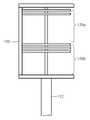
도 4는 도 1에 도시한 버퍼 챔버를 나타내는 도면이며, 도 5는 도 4에 도시한 기판 홀더를 나타내는 도면이다. 버퍼 챔버(110)는 상부챔버(110a)와 하부챔버(110b)를 구비한다. 하부 챔버(110b)는 이송 챔버(102)에 대응되는 일측에 형성된 통로(110c)를 구비하며, 기판(S)은 통로(110c)를 통해 이송 챔버(102)로부터 버퍼 챔버(110)로 로딩된다. 이송 챔버(102)는 버퍼 챔버(110)에 대응되는 일측에 형성된 버퍼 통로(102a)를 가지며, 버퍼 통로(102a)와 통로(110c) 사이에는 게이트 밸브(103)가 설치된다. 게이트 밸브(103)는 이송 챔버(102)와 버퍼 챔버(110)를 격리할 수 있으며, 버퍼 통로(102a)와 통로(110c)는 게이트 밸브(103)를 통해 개방 및 폐쇄될 수 있다.
4 is a view showing the buffer chamber shown in FIG. 1, and FIG. 5 is a view showing the substrate holder shown in FIG. The
버퍼 챔버(110)는 기판(S)이 적재되는 기판 홀더(120)를 구비하며, 기판(S)은 기판 홀더(120) 상에 종방향으로 적재된다. 기판 홀더(120)는 승강축(122)에 연결되며, 승강축(122)은 하부챔버(110b)를 관통하여 지지판(124) 및 구동축(128)에 연결된다. 구동축(128)은 엘리베이터(129)를 통해 승강하며, 구동축(128)에 의해 승강축(122) 및 기판 홀더(120)는 승강할 수 있다.
The
기판 핸들러(104)는 세정 공정이 완료된 기판(S)을 버퍼 챔버(110)로 순차적으로 이송한다. 이때, 기판 홀더(120)는 엘리베이터(129)에 의해 승강하며, 승강에 의해 기판 홀더(120)의 비어 있는 슬롯을 통로(110c)와 대응되는 위치로 이동한다. 따라서, 버퍼 챔버(110)로 이송된 기판(S)은 기판 홀더(120) 상에 적재되며, 기판 홀더(120)의 승강에 의해 기판(S)은 종방향으로 적재될 수 있다.
The
한편, 도 5에 도시한 바와 같이, 기판 홀더(120)는 상부적재공간(120a)과 하부적재공간(120b)을 구비한다. 앞서 설명한 바와 같이, 세정 공정을 완료한 기판(S) 및 에피택셜 공정을 완료한 기판(S)은 기판 홀더(120) 상에 적재된다. 따라서, 세정 공정을 완료한 기판(S)과 에피택셜 공정을 완료한 기판(S)은 구별될 필요가 있으며, 세정 공정을 완료한 기판(S)은 상부적재공간(120a)에 적재되고, 에피택셜 공정을 완료한 기판(S)은 하부적재공간(120b)에 적재된다. 상부적재공간(120a)은 13장의 기판들(S)을 적재할 수 있으며, 하나의 에피택셜 챔버(112a,112b,112c)는 13장의 기판들(S)에 대한 공정을 처리할 수 있다. 마찬가지로, 하부적재공간(120b)은 13장의 기판들(S)을 적재할 수 있다.
Meanwhile, as shown in FIG. 5, the
하부챔버(110b)는 배기라인(132)에 연결되며, 배기펌프(132b)를 통해 버퍼 챔버(110)의 내부는 진공 상태를 유지할 수 있다. 밸브(132a)는 배기라인(132)을 개폐한다. 벨로우즈(126)는 하부챔버(110b)의 하부와 지지판(124)을 연결하며, 벨로우즈(126)를 통해 버퍼 챔버(110)의 내부는 밀봉될 수 있다. 즉, 벨로우즈(126)는 승강축(122)의 둘레를 통한 진공 누출을 방지한다.
The
도 6은 도 1에 도시한 세정 챔버를 나타내는 도면이다. 앞서 설명한 바와 같이, 세정 챔버(108a,108b)는 동일한 공정을 수행하는 챔버일 수 있으며, 이하에서는 하나의 세정 챔버(108a)에 대해서만 설명하기로 한다.
FIG. 6 is a view showing the cleaning chamber shown in FIG. 1. As described above, the
세정 챔버(108a)는 상부챔버(118a)와 하부챔버(118b)를 구비하며, 상부챔버(118a)와 하부챔버(118b)는 상하로 적재될 수 있다. 상부챔버(118a) 및 하부챔버(118b)는 이송 챔버(102)에 대응되는 일측에 형성된 상부통로(128a) 및 하부통로(138a)를 각각 구비하며, 기판(S)은 상부통로(128a) 및 하부통로(138a)를 통해 이송 챔버(102)로부터 상부챔버(118a) 및 하부챔버(118b)로 각각 로딩될 수 있다. 이송 챔버(102)는 상부챔버(118a) 및 하부챔버(118b)에 각각 대응되는 일측에 형성된 상부 통로(102b) 및 하부 통로(102a)를 가지며, 상부 통로(102b)와 상부통로(128a) 사이에는 상부 게이트 밸브(105a)가 설치되고, 하부 통로(102a)와 하부통로(138a) 사이에는 하부 게이트 밸브(105b)가 설치된다. 게이트 밸브(105a,105b)는 상부챔버(118a)와 이송 챔버(102), 그리고 하부챔버(118b)와 이송 챔버(102)를 각각 격리할 수 있다. 상부 통로(102b)와 상부통로(128a)는 상부 게이트 밸브(105a)를 통해 개방 및 폐쇄될 수 있으며, 하부 통로(102a)와 하부통로(138a)는 하부 게이트 밸브(105b)를 통해 개방 및 폐쇄될 수 있다.
The
상부챔버(118a)는 기판(S)에 대하여 라디칼을 이용한 반응 공정을 진행하며, 상부챔버(118a)는 라디칼 공급라인(116a) 및 가스공급라인(116b)에 연결된다. 라디칼 공급라인은 라디칼 생성가스(예를 들어, H2 또는 NH3)가 충전된 가스용기(도시안함)와 캐리어 가스(N2)가 충전된 가스 용기(도시안함)에 연결되며, 각 가스 용기의 밸브를 개방하면 라디칼 생성가스와 캐리어 가스가 상부챔버(118a)의 내부로 공급된다. 또한, 라디칼 공급라인(116a)은 도파관(도시안함)을 통해 마이크로파원(도시안함)에 접속되며, 마이크로파원이 마이크로파를 발생시키면 마이크로파는 도파관을 진행하여 라디칼 공급라인(116a) 내부로 침입한다. 그 상태에서 라디칼 생성가스가 흐르면 마이크로파에 의해 플라즈마화되어 라디칼이 생성된다. 생성된 라디칼은 미처리된 라디칼 생성가스나 캐리어 가스, 그리고 플라즈마화의 부생성물과 함께 라디칼 공급라인(116a)을 흘러 상부챔버(118a)의 내부로 도입된다. 한편, 본 실시예와 달리, 라디칼은 ICP 방식의 리모트 플라즈마에 의해서도 생성될 수 있다. 즉, ICP 방식의 리모트 플라즈마 소스에 라디칼 생성가스가 공급되면, 라디칼 생성가스는 플라즈마화되어 라디칼이 생성된다. 생성된 라디칼은 라디칼 공급라인(116a)을 흘러 상부챔버(118a)의 내부로 도입될 수 있다.
The
라디칼 공급라인(116a)을 통해 상부챔버(118a) 내부에 라디칼(예를 들어, 수소 라디칼)이 공급되고, 가스공급라인(116b)을 통해 상부챔버(118a) 내부에 반응성 가스(예를 들어, NF3와 같은 불화물 가스)가 공급되며, 이들을 혼합시켜 반응시킨다. 이 경우, 반응식은 아래와 같다.
Radicals (eg, hydrogen radicals) are supplied into the


즉, 기판(S)의 표면에 미리 흡착한 반응성 가스와 라디칼이 반응하여 중간 생성물(NHxFy)이 생성되고, 중간생성물(NHxFy)과 기판(S) 표면의 자연 산화막(SiO2)이 반응하여 반응 생성물((NH4F)SiF6)이 형성된다. 한편, 기판(S)은 상부챔버(118a) 내에 설치된 서셉터(128)에 놓여지며, 서셉터(128)는 반응공정 동안 기판(S)을 회전시켜 균일한 반응이 이루어질 수 있도록 돕는다.
That is, the reactive gas and radicals previously adsorbed on the surface of the substrate S react with each other to produce an intermediate product NHx Fy , and the intermediate product NHx Fy and the natural oxide film SiO on the substrate S surface.2 ) reacts to form a reaction product ((NH4 F) SiF6 ). Meanwhile, the substrate S is placed in the
상부챔버(118a)는 배기라인(119a)에 연결되며, 배기펌프(119c)를 통해 반응 공정이 이루어지기 전 상부챔버(118a)에 대한 진공 배기를 할 수 있을 뿐만 아니라, 상부챔버(118a) 내부의 라디칼과 반응성 가스, 미반응 라디칼 생성가스, 플라즈마화할 때의 부생성물, 캐리어 가스 등을 외부로 배출할 수 있다. 밸브(119b)는 배기라인(119a)을 개폐한다.
The
하부챔버(118b)는 기판(S)에 대한 히팅공정을 진행하며, 하부챔버(118b)의 내측 상부에는 히터(148)가 설치된다. 반응 공정이 완료되면, 기판(S)은 기판 핸들러(104)를 통해 하부챔버(118b)로 이송된다. 이때, 기판(S)은 진공 상태를 유지하는 이송 챔버(102)를 통해 이송되므로, 기판(S)이 오염물(예를 들면, O2, 입자상 물질 등)에 노출되는 것을 방지할 수 있다.
The
히터(148)는 기판(S)을 소정 온도(100℃ 이상의 소정 온도, 예를 들어, 130℃)로 가열하며, 이로 인해 반응 생성물이 열분해하여 기판(S) 표면으로부터 HF나 SiF4와 같은 열분해 가스가 이탈되고, 진공배기됨으로써 기판(S)의 표면으로부터 실리콘 산화물의 박막이 제거될 수 있다. 기판(S)은 히터(148)의 하부에 설치된 서셉터(138)에 놓여지며, 히터(148)는 서셉터(138)에 놓여진 기판(S)을 가열한다.
The

한편, 하부챔버(118b)는 배기라인(117a)에 연결되며, 배기펌프(117c)를 통해 하부챔버(118b) 내부의 반응부산물(예를 들어, NH3, HF, SiF4)을 외부로 배기할 수 있다. 밸브(117b)는 배기라인(117a)을 개폐한다.
Meanwhile, the
도 7은 도 1에 도시한 세정 챔버의 다른 실시예를 나타내는 도면이다. 세정 챔버(108a)는 상부챔버(218a)와 하부챔버(218b)를 구비하며, 상부챔버(218a)와 하부챔버(218b)는 서로 연통된다. 하부 챔버(218b)는 이송 챔버(102)에 대응되는 일측에 형성된 통로(219)를 가지며, 기판(S)은 통로(219)를 통해 이송 챔버(102)로부터 세정 챔버(108a)로 로딩될 수 있다. 이송 챔버(102)는 세정 챔버(108a)에 대응되는 일측에 형성된 이송 통로(102d)를 가지며, 이송 통로(102d)와 통로(219) 사이에는 게이트 밸브(107)가 설치된다. 게이트 밸브(107)는 이송 챔버(102)와 세정 챔버(108a)를 격리할 수 있으며, 이송 통로(102d)와 통로(219)는 게이트 밸브(107)를 통해 개방 및 폐쇄될 수 있다.
7 is a view showing another embodiment of the cleaning chamber shown in FIG. 1. The
세정 챔버(108a)는 기판(S)이 적재되는 기판 홀더(228)를 구비하며, 기판(S)은 기판 홀더(228) 상에 종방향으로 적재된다. 기판 홀더(228)는 회전축(226)에 연결되며, 회전축(226)은 하부챔버(218b)를 관통하여 엘리베이터(232) 및 구동모터(234)에 연결된다. 회전축(226)은 엘리베이터(232)를 통해 승강하며, 기판 홀더(228)는 회전축(226)과 함께 승강할 수 있다. 회전축(226)은 구동모터(234)를 통해 회전하며, 기판 홀더(228)는 에칭 공정이 이루어지는 동안 회전축(226)과 함께 회전할 수 있다.
The
기판 핸들러(104)는 기판(S)을 세정 챔버(108a)로 순차적으로 이송한다. 이때, 기판 홀더(228)는 엘리베이터(232)에 의해 승강하며, 승강에 의해 기판 홀더(228)의 비어 있는 슬롯을 통로(219)와 대응되는 위치로 이동한다. 따라서, 세정 챔버(108a)로 이송된 기판(S)은 기판 홀더(228) 상에 적재되며, 기판 홀더(228)의 승강에 의해 기판(S)은 종방향으로 적재될 수 있다. 기판 홀더(228)는 13장의 기판들(S)을 적재할 수 있다.
The
기판 홀더(228)가 하부챔버(218b) 내에 위치하는 동안, 기판(S)은 기판 홀더(228) 내에 적재되며, 도 7에 도시한 바와 같이, 기판 홀더(228)가 상부챔버(218a)에 위치하는 동안, 기판(S)에 대한 세정 공정이 이루어진다. 상부챔버(218a)는 세정 공정이 이루어지는 공정공간을 제공한다. 지지판(224)은 회전축(226) 상에 설치되며, 기판 홀더(228)와 함께 상승하여 상부챔버(218a) 내부의 공정공간을 외부로부터 차단한다. 지지판(224)은 하부챔버(218b)의 상단부에 인접하도록 배치되며, 지지판(224)과 하부챔버(218b)의 상단부 사이에는 실링부재(224a)(예를 들어, O-링과 같은)가 개재되어 공정공간을 밀폐한다. 지지판(224)과 회전축(226) 사이에는 베어링부재(224b)가 설치되며, 회전축(226)은 베어링부재(224b)에 의해 지지된 상태에서 회전할 수 있다.
While the
기판(S)에 대한 반응공정 및 히팅공정은 상부챔버(218a) 내부의 공정공간 내에서 이루어진다. 기판 홀더(228)에 기판(S)이 모두 적재되면, 기판 홀더(228)는 엘리베이터(232)에 의해 상승하여 상부챔버(218a) 내부의 공정공간으로 이동한다. 인젝터(216)는 상부챔버(218a) 내부의 일측에 설치되며, 인젝터(216)는 복수의 인젝트홀들(216a)을 가진다.
The reaction process and the heating process for the substrate S are performed in the process space inside the
인젝터(216)는 라디칼 공급라인(215a)에 연결된다. 또한, 상부챔버(218a)는 가스공급라인(215b)에 연결된다. 라디칼 공급라인(215a)은 라디칼 생성가스(예를 들어, H2 또는 NH3)가 충전된 가스용기(도시안함)와 캐리어 가스(N2)가 충전된 가스 용기(도시안함)에 연결되며, 각 가스 용기의 밸브를 개방하면 라디칼 생성가스와 캐리어 가스가 인젝터(216)를 통해 공정공간으로 공급된다. 또한, 라디칼 공급라인(215a)은 도파관(도시안함)을 통해 마이크로파원(도시안함)에 접속되며, 마이크로파원이 마이크로파를 발생시키면 마이크로파는 도파관을 진행하여 라디칼 공급라인(215a) 내부로 침입한다. 그 상태에서 라디칼 생성가스가 흐르면 마이크로파에 의해 플라즈마화되어 라디칼이 생성된다. 생성된 라디칼은 미처리된 라디칼 생성가스나 캐리어 가스, 그리고 플라즈마화의 부생성물과 함께 라디칼 공급라인(215a)을 흘러 인젝터(216)에 공급되며, 인젝터(216)를 통해 공정공간으로 도입된다. 한편, 본 실시예와 달리, 라디칼은 ICP 방식의 리모트 플라즈마에 의해서도 생성될 수 있다. 즉, ICP 방식의 리모트 플라즈마 소스에 라디칼 생성가스가 공급되면, 라디칼 생성가스는 플라즈마화되어 라디칼이 생성된다. 생성된 라디칼은 라디칼 공급라인(215a)을 흘러 상부챔버(218a)의 내부로 도입될 수 있다.
The
라디칼 공급라인(215a)을 통해 상부챔버(218a) 내부에 라디칼(예를 들어, 수소 라디칼)이 공급되고, 가스공급라인(215b)을 통해 상부챔버(218a) 내부에 반응성 가스(예를 들어, NF3와 같은 불화물 가스)가 공급되며, 이들을 혼합시켜 반응시킨다. 이 경우, 반응식은 아래와 같다.
Radicals (eg, hydrogen radicals) are supplied into the


즉, 기판(S)의 표면에 미리 흡착한 반응성 가스와 라디칼이 반응하여 중간 생성물(NHxFy)이 생성되고, 중간생성물(NHxFy)과 기판(S) 표면의 자연 산화막(SiO2)이 반응하여 반응 생성물((NH4F)SiF6)이 형성된다. 한편, 기판 홀더(228)는 에칭공정 동안 기판(S)을 회전시켜 균일한 에칭이 이루어질 수 있도록 돕는다.
That is, the reactive gas and radicals previously adsorbed on the surface of the substrate S react with each other to produce an intermediate product NHx Fy , and the intermediate product NHx Fy and the natural oxide film SiO on the substrate S surface.2 ) reacts to form a reaction product ((NH4 F) SiF6 ). On the other hand, the
상부챔버(218a)는 배기라인(217)에 연결되며, 배기펌프(217b)를 통해 반응 공정이 이루어지기 전 상부챔버(218a)에 대한 진공 배기를 할 수 있을 뿐만 아니라, 상부챔버(218a) 내부의 라디칼과 반응성 가스, 미반응 라디칼 생성가스, 플라즈마화할 때의 부생성물, 캐리어 가스 등을 외부로 배출할 수 있다. 밸브(217a)는 배기라인(217)을 개폐한다.
The
히터(248)는 상부챔버(218a)의 타측에 설치되며, 히터(248)는 반응 공정이 완료된 후 기판(S)을 소정 온도(100℃ 이상의 소정 온도, 예를 들어, 130℃)로 가열한다. 이로 인해 반응 생성물이 열분해하여 기판(S) 표면으로부터 HF나 SiF4와 같은 열분해 가스가 이탈되고, 진공배기됨으로써 기판(S)의 표면으로부터 실리콘 산화물의 박막이 제거될 수 있다. 반응부산물(예를 들어, NH3, HF, SiF4)은 배기라인(217)을 통해 외부로 배출될 수 있다.
The

도 8은 도 1에 도시한 에피택셜 챔버를 나타내는 도면이며, 도 9는 도 1에 도시한 공급관을 나타내는 도면이다. 에피택셜 챔버(112a,112b,112c)는 동일한 공정을 수행하는 챔버일 수 있으며, 이하에서는 하나의 에피택셜 챔버(112a)에 대해서만 설명하기로 한다.
FIG. 8 is a view showing the epitaxial chamber shown in FIG. 1, and FIG. 9 is a view showing the supply pipe shown in FIG. The
에피택셜 챔버(112a)는 상부챔버(312a)와 하부챔버(312b)를 구비하며, 상부챔버(312a)와 하부챔버(312b)는 서로 연통된다. 하부 챔버(312b)는 이송 챔버(102)에 대응되는 일측에 형성된 통로(319)를 가지며, 기판(S)은 통로(319)를 통해 이송 챔버(102)로부터 에피택셜 챔버(112a)로 로딩될 수 있다. 이송 챔버(102)는 에피택셜 챔버(112a)에 대응되는 일측에 형성된 이송 통로(102e)를 가지며, 이송 통로(102e)와 통로(319) 사이에는 게이트 밸브(109)가 설치된다. 게이트 밸브(109)는 이송 챔버(102)와 에피택셜 챔버(112a)를 격리할 수 있으며, 이송 통로(102e)와 통로(319)는 게이트 밸브(109)를 통해 개방 및 폐쇄될 수 있다.
The
에피택셜 챔버(112a)는 기판(S)이 적재되는 기판 홀더(328)를 구비하며, 기판(S)은 기판 홀더(328) 상에 종방향으로 적재된다. 기판 홀더(328)는 회전축(318)에 연결되며, 회전축(318)은 하부챔버(312b)를 관통하여 엘리베이터(319a) 및 구동모터(319b)에 연결된다. 회전축(318)은 엘리베이터(319a)를 통해 승강하며, 기판 홀더(328)는 회전축(318)과 함께 승강할 수 있다. 회전축(318)은 구동모터(319b)를 통해 회전하며, 기판 홀더(328)는 에피택셜 공정이 이루어지는 동안 회전축(318)과 함께 회전할 수 있다.
The
기판 핸들러(104)는 기판(S)을 에피택셜 챔버(112a)로 순차적으로 이송한다. 이때, 기판 홀더(328)는 엘리베이터(319a)에 의해 승강하며, 승강에 의해 기판 홀더(328)의 비어 있는 슬롯을 통로(319)와 대응되는 위치로 이동한다. 따라서, 에피택셜 챔버(112a)로 이송된 기판(S)은 기판 홀더(328) 상에 적재되며, 기판 홀더(328)의 승강에 의해 기판(S)은 종방향으로 적재될 수 있다. 기판 홀더(328)는 13장의 기판들(S)을 적재할 수 있다.
The
기판 홀더(328)가 하부챔버(312b) 내에 위치하는 동안, 기판(S)은 기판 홀더(328) 내에 적재되며, 도 8에 도시한 바와 같이, 기판 홀더(328)가 반응튜브(314) 내에 위치하는 동안, 기판(S)에 대한 에피택셜 공정이 이루어진다. 반응튜브(314)는 에피택셜 공정이 이루어지는 공정공간을 제공한다. 지지판(316)은 회전축(318) 상에 설치되며, 기판 홀더(328)와 함께 상승하여 반응튜브(314) 내부의 공정공간을 외부로부터 차단한다. 지지판(316)은 반응튜브(314)의 하단부에 인접하도록 배치되며, 지지판(316)과 반응튜브(314)의 하단부 사이에는 실링부재(316a)(예를 들어, O-링과 같은)가 개재되어 공정공간을 밀폐한다. 지지판(316)과 회전축(318) 사이에는 베어링부재(316b)가 설치되며, 회전축(318)은 베어링부재(316b)에 의해 지지된 상태에서 회전할 수 있다.
While the
기판(S)에 대한 에피택셜 공정은 반응튜브(314) 내부의 공정공간 내에서 이루어진다. 공급관(332)은 반응튜브(314) 내부의 일측에 설치되며, 배기관(334)은 반응튜브(314) 내부의 타측에 설치된다. 공급관(332) 및 배기관(334)은 기판(S)을 중심으로 서로 마주보도록 배치될 수 있으며, 기판(S)의 적재방향에 따라 종방향으로 배치될 수 있다. 측부히터(324) 및 상부히터(326)는 반응튜브(314)의 외측에 설치되며, 반응튜브(314) 내부의 공정공간을 가열한다.
The epitaxial process on the substrate S is performed in the process space inside the
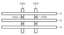
공급관(332)은 공급라인(332a)에 연결되며, 공급라인(332a)은 반응가스 소스(332c)에 연결된다. 반응가스는 반응가스 소스(332c)에 저장되며, 공급라인(332a)을 통해 공급관(332)에 공급된다. 도 9에 도시한 바와 같이, 공급관(332)은 제1 및 제2 공급관(332a,332b)을 구비할 수 있으며, 제1 및 제2 공급관(332a,332b)은 길이방향을 따라 이격배치된 복수의 공급홀들(333a,333b)을 가진다. 이때, 공급홀들(333a,333b)은 반응튜브(314)에 로딩된 기판(S)의 개수와 대체로 동일하게 형성되며, 기판(S)의 사이에 대응되도록 위치하거나 기판(S)과 무관하게 위치할 수 있다. 따라서, 공급홀들(333a,333b)을 통해 공급된 반응가스는 기판(S)의 표면을 따라 층류 상태(larminar flow)로 원활하게 흐를 수 있으며, 기판(S)이 가열된 상태에서 기판(S) 상에 에피택셜 층이 형성될 수 있다. 공급라인(332a)은 밸브(332b)를 통해 개폐될 수 있다.
한편, 제1 공급관(332a)은 증착용 가스(실리콘 가스(예를 들어, SiCl4, SiHCl3, SiH2Cl2, SiH3Cl, Si2H6, 또는 SiH4) 및 캐리어 가스(예를 들어, N2 및/또는 H2))를 공급하며, 제2 공급관(332b)은 에칭용 가스를 공급할 수 있다. 선택적 에피택시 프로세스(selective epitaxy process)는 증착 반응 및 에칭 반응을 수반한다. 본 실시예에서는 도시하지 않았지만, 에피택시 층이 도펀트를 포함할 것이 요구되는 경우, 제3 공급관이 추가될 수 있으며, 제3 공급관은 도펀트 함유 가스(예를 들면, 아르신(AsH3), 포스핀(PH3), 및/또는 디보란(B2H6))를 공급할 수 있다.
Meanwhile, the
배기관(334)은 배기라인(335a)에 연결되며, 배기펌프(335)를 통해 반응튜브(314) 내부의 반응부산물을 외부로 배기할 수 있다. 배기관(334)은 복수의 배기홀들을 가지며, 배기홀들은 공급홀들(333a,333b)과 마찬가지로 기판(S)의 사이에 대응되도록 위치하거나 기판(S)과 무관하게 위치할 수 있다. 밸브(335b)는 배기라인(335a)을 개폐한다.
The
본 발명을 바람직한 실시예들을 통하여 상세하게 설명하였으나, 이와 다른 형태의 실시예들도 가능하다. 그러므로, 이하에 기재된 청구항들의 기술적 사상과 범위는 바람직한 실시예들에 한정되지 않는다.Although the present invention has been described in detail by way of preferred embodiments thereof, other forms of embodiment are possible. Therefore, the technical idea and scope of the claims set forth below are not limited to the preferred embodiments.
1 : 반도체 제조설비2 : 공정모듈
3 : 설비 전방 단부 모듈4 : 경계벽
60 : 로드포트70 : 기판
72 : 산화막74 : 에피택시 표면
102 : 이송 챔버103,105a,105b,107 : 게이트 밸브
104 : 기판 핸들러108a,108b : 세정 챔버
110 : 버퍼 챔버112a,112b,112c : 에피택셜 챔버
118a : 에칭 챔버118b : 히팅 챔버
120,228,328 : 기판 홀더148,248,324,326 : 히터
216 : 인젝터224,316 : 지지판
332 : 공급관334 : 배기관1: Semiconductor manufacturing facility 2: Process module
3 facility
60: load port 70: substrate
72: oxide film 74: epitaxial surface
102:
104:
110:
118a: etching
120,228,328: substrate holder 148,248,324,326: heater
216: injector 224,316: support plate
332
Claims (7)
Translated fromKorean상기 기판 상에 에피택셜 층을 형성하는 에피택셜 공정이 이루어지는 에피택셜 챔버;
상기 기판이 적재되는 적재공간을 구비하는 기판 홀더를 구비하며, 상기 적재공간은 상기 세정 공정이 완료된 상기 기판이 적재되는 제1 적재공간과 상기 에피택셜 층이 형성된 상기 기판이 적재되는 제2 적재공간을 구비하는 버퍼 챔버; 및
상기 세정 챔버 및 상기 버퍼 챔버, 그리고 상기 에피택셜 챔버가 측면에 연결되며, 상기 세정 챔버 및 상기 버퍼 챔버, 그리고 상기 에피택셜 챔버 사이에서 상기 기판을 이송하는 기판 핸들러를 구비하는 이송 챔버를 포함하며,
상기 기판 핸들러는 상기 세정 공정이 완료된 상기 기판을 상기 버퍼 챔버에 순차적으로 이송하고 상기 버퍼 챔버에 적재된 상기 기판을 상기 에피택셜 챔버로 이송하며, 상기 에피택셜 층이 형성된 상기 기판을 상기 버퍼 챔버에 순차적으로 이송하는, 반도체 제조설비.A batch type cleaning chamber in which a cleaning process is performed on the plurality of substrates;
An epitaxial chamber in which an epitaxial process of forming an epitaxial layer is formed on the substrate;
And a substrate holder having a loading space on which the substrate is loaded, wherein the loading space includes a first loading space on which the substrate on which the cleaning process is completed is loaded and a second loading space on which the substrate on which the epitaxial layer is formed is loaded. A buffer chamber having a; And
A transfer chamber coupled to the cleaning chamber, the buffer chamber, and the epitaxial chamber, the transfer chamber having a substrate handler for transferring the substrate between the cleaning chamber, the buffer chamber, and the epitaxial chamber,
The substrate handler sequentially transfers the substrate on which the cleaning process is completed, to the buffer chamber, transfers the substrate loaded on the buffer chamber to the epitaxial chamber, and transfers the substrate on which the epitaxial layer is formed to the buffer chamber. The semiconductor manufacturing equipment which transfers sequentially.
상기 세정 챔버는,
상기 세정 공정이 이루어지는 공정공간을 제공하는 상부챔버;
상기 기판이 출입하는 세정 통로를 가지는 하부챔버;
상기 기판이 적재되는 기판 홀더;
상기 기판 홀더에 연결되어 상기 기판 홀더와 함께 승강하며, 상기 기판 홀더를 상기 상부챔버 및 상기 하부챔버로 이동하는 회전축; 및
상기 기판 홀더와 함께 승강하며, 상기 세정 공정 동안 상기 공정공간을 외부로부터 차단하는 지지판을 구비하는 것을 특징으로 하는 반도체 제조설비.The method of claim 1,
The cleaning chamber includes:
An upper chamber providing a process space in which the cleaning process is performed;
A lower chamber having a cleaning passage through which the substrate enters and exits;
A substrate holder on which the substrate is loaded;
A rotating shaft connected to the substrate holder to move together with the substrate holder to move the substrate holder to the upper chamber and the lower chamber; And
And a support plate which is lifted up and down with the substrate holder and blocks the process space from the outside during the cleaning process.
상기 세정 챔버는 상기 회전축을 승강하는 엘리베이터 및 상기 회전축을 회전시키는 구동모터를 더 구비하는 것을 특징으로 하는 반도체 제조설비.The method of claim 2,
The cleaning chamber further comprises an elevator for lifting and lowering the rotating shaft and a driving motor for rotating the rotating shaft.
상기 세정 챔버는,
상기 상부챔버의 일측에 설치되어 상기 공정공간을 향해 라디칼을 공급하는 인젝터;
상기 인젝터에 연결되어 상기 인젝터에 상기 라디칼을 공급하는 라디칼 공급라인; 및
상기 상부챔버에 연결되어 상기 공정공간을 향해 반응성 가스를 공급하는 가스공급라인을 구비하는 것을 특징으로 하는 반도체 제조설비.The method of claim 2,
The cleaning chamber includes:
An injector installed at one side of the upper chamber to supply radicals toward the process space;
A radical supply line connected to the injector to supply the radicals to the injector; And
And a gas supply line connected to the upper chamber and supplying a reactive gas toward the process space.
상기 반응성 가스는 NF3를 포함하는 불화물 가스인 것을 특징으로 하는 반도체 제조설비.5. The method of claim 4,
The reactive gas is a semiconductor manufacturing equipment, characterized in that the fluoride gas containing NF3 .
상기 세정 챔버는 상기 상부챔버의 일측에 설치되어 상기 공정공간을 가열하는 히터를 더 구비하는 것을 특징으로 하는 반도체 제조설비.The method of claim 2,
The cleaning chamber is installed on one side of the upper chamber semiconductor manufacturing equipment, characterized in that further comprising a heater for heating the process space.
상기 이송 챔버는 상기 세정 챔버를 향해 상기 기판이 출입하는 이송 통로를 가지며,
상기 반도체 제조설비는 상기 세정 챔버와 상기 이송 챔버를 격리하는 세정측 게이트 밸브를 더 포함하는 것을 특징으로 하는 반도체 제조설비.5. The method according to any one of claims 1 to 4,
The transfer chamber has a transfer passage through which the substrate enters and exits toward the cleaning chamber,
The semiconductor manufacturing facility further comprises a cleaning side gate valve separating the cleaning chamber and the transfer chamber.
Priority Applications (7)
| Application Number | Priority Date | Filing Date | Title |
|---|---|---|---|
| KR1020110077102AKR101271248B1 (en) | 2011-08-02 | 2011-08-02 | Equipment for manufacturing semiconductor |
| TW101126742ATWI474422B (en) | 2011-08-02 | 2012-07-25 | Equipment for manufacturing semiconductor |
| PCT/KR2012/006107WO2013019064A2 (en) | 2011-08-02 | 2012-07-31 | Equipment for manufacturing semiconductor for epitaxial process |
| US14/235,313US20140174357A1 (en) | 2011-08-02 | 2012-07-31 | Equipment for manufacturing semiconductor |
| JP2014523843AJP5978301B2 (en) | 2011-08-02 | 2012-07-31 | Semiconductor manufacturing equipment for epitaxial processes |
| CN201280037898.9ACN103828024B (en) | 2011-08-02 | 2012-07-31 | Semiconductor manufacturing facility for epitaxy technique |
| US15/842,099US20180105951A1 (en) | 2011-08-02 | 2017-12-14 | Equipment for manufacturing semiconductor |
Applications Claiming Priority (1)
| Application Number | Priority Date | Filing Date | Title |
|---|---|---|---|
| KR1020110077102AKR101271248B1 (en) | 2011-08-02 | 2011-08-02 | Equipment for manufacturing semiconductor |
Publications (2)
| Publication Number | Publication Date |
|---|---|
| KR20130015224A KR20130015224A (en) | 2013-02-13 |
| KR101271248B1true KR101271248B1 (en) | 2013-06-07 |
Family
ID=47629799
Family Applications (1)
| Application Number | Title | Priority Date | Filing Date |
|---|---|---|---|
| KR1020110077102AActiveKR101271248B1 (en) | 2011-08-02 | 2011-08-02 | Equipment for manufacturing semiconductor |
Country Status (6)
| Country | Link |
|---|---|
| US (2) | US20140174357A1 (en) |
| JP (1) | JP5978301B2 (en) |
| KR (1) | KR101271248B1 (en) |
| CN (1) | CN103828024B (en) |
| TW (1) | TWI474422B (en) |
| WO (1) | WO2013019064A2 (en) |
Cited By (1)
| Publication number | Priority date | Publication date | Assignee | Title |
|---|---|---|---|---|
| WO2021257889A1 (en)* | 2020-06-19 | 2021-12-23 | Applied Materials, Inc. | Batch wafer degas chamber and integration into factory interface and vacuum-based mainframe |
Families Citing this family (280)
| Publication number | Priority date | Publication date | Assignee | Title |
|---|---|---|---|---|
| US20130023129A1 (en) | 2011-07-20 | 2013-01-24 | Asm America, Inc. | Pressure transmitter for a semiconductor processing environment |
| KR101271246B1 (en)* | 2011-08-02 | 2013-06-07 | 주식회사 유진테크 | Equipment for manufacturing semiconductor |
| KR20140023807A (en)* | 2012-08-17 | 2014-02-27 | 삼성전자주식회사 | Apparatus of fabricating semiconductor devices |
| US10714315B2 (en) | 2012-10-12 | 2020-07-14 | Asm Ip Holdings B.V. | Semiconductor reaction chamber showerhead |
| US20160376700A1 (en) | 2013-02-01 | 2016-12-29 | Asm Ip Holding B.V. | System for treatment of deposition reactor |
| KR101677560B1 (en)* | 2014-03-18 | 2016-11-18 | 주식회사 유진테크 | Apparatus for processing substrate with heater adjusting process space temperature according to height |
| US11015245B2 (en) | 2014-03-19 | 2021-05-25 | Asm Ip Holding B.V. | Gas-phase reactor and system having exhaust plenum and components thereof |
| US10941490B2 (en) | 2014-10-07 | 2021-03-09 | Asm Ip Holding B.V. | Multiple temperature range susceptor, assembly, reactor and system including the susceptor, and methods of using the same |
| US10276355B2 (en) | 2015-03-12 | 2019-04-30 | Asm Ip Holding B.V. | Multi-zone reactor, system including the reactor, and method of using the same |
| CN104766814A (en)* | 2015-03-31 | 2015-07-08 | 上海华力微电子有限公司 | Device and method for preventing growth of natural oxidation film in wet cleaning process |
| KR101720620B1 (en)* | 2015-04-21 | 2017-03-28 | 주식회사 유진테크 | Substrate Processing Apparatus and Method of Cleaning Chamber |
| US10458018B2 (en) | 2015-06-26 | 2019-10-29 | Asm Ip Holding B.V. | Structures including metal carbide material, devices including the structures, and methods of forming same |
| US10211308B2 (en) | 2015-10-21 | 2019-02-19 | Asm Ip Holding B.V. | NbMC layers |
| US11139308B2 (en) | 2015-12-29 | 2021-10-05 | Asm Ip Holding B.V. | Atomic layer deposition of III-V compounds to form V-NAND devices |
| US10529554B2 (en) | 2016-02-19 | 2020-01-07 | Asm Ip Holding B.V. | Method for forming silicon nitride film selectively on sidewalls or flat surfaces of trenches |
| US10343920B2 (en) | 2016-03-18 | 2019-07-09 | Asm Ip Holding B.V. | Aligned carbon nanotubes |
| US10367080B2 (en) | 2016-05-02 | 2019-07-30 | Asm Ip Holding B.V. | Method of forming a germanium oxynitride film |
| US11453943B2 (en) | 2016-05-25 | 2022-09-27 | Asm Ip Holding B.V. | Method for forming carbon-containing silicon/metal oxide or nitride film by ALD using silicon precursor and hydrocarbon precursor |
| US10612137B2 (en) | 2016-07-08 | 2020-04-07 | Asm Ip Holdings B.V. | Organic reactants for atomic layer deposition |
| US9859151B1 (en) | 2016-07-08 | 2018-01-02 | Asm Ip Holding B.V. | Selective film deposition method to form air gaps |
| US9812320B1 (en) | 2016-07-28 | 2017-11-07 | Asm Ip Holding B.V. | Method and apparatus for filling a gap |
| US9887082B1 (en) | 2016-07-28 | 2018-02-06 | Asm Ip Holding B.V. | Method and apparatus for filling a gap |
| KR102532607B1 (en) | 2016-07-28 | 2023-05-15 | 에이에스엠 아이피 홀딩 비.브이. | Substrate processing apparatus and method of operating the same |
| US11532757B2 (en) | 2016-10-27 | 2022-12-20 | Asm Ip Holding B.V. | Deposition of charge trapping layers |
| US10714350B2 (en) | 2016-11-01 | 2020-07-14 | ASM IP Holdings, B.V. | Methods for forming a transition metal niobium nitride film on a substrate by atomic layer deposition and related semiconductor device structures |
| KR102546317B1 (en) | 2016-11-15 | 2023-06-21 | 에이에스엠 아이피 홀딩 비.브이. | Gas supply unit and substrate processing apparatus including the same |
| KR102762543B1 (en) | 2016-12-14 | 2025-02-05 | 에이에스엠 아이피 홀딩 비.브이. | Substrate processing apparatus |
| US11447861B2 (en) | 2016-12-15 | 2022-09-20 | Asm Ip Holding B.V. | Sequential infiltration synthesis apparatus and a method of forming a patterned structure |
| US11581186B2 (en) | 2016-12-15 | 2023-02-14 | Asm Ip Holding B.V. | Sequential infiltration synthesis apparatus |
| KR102700194B1 (en) | 2016-12-19 | 2024-08-28 | 에이에스엠 아이피 홀딩 비.브이. | Substrate processing apparatus |
| US10269558B2 (en) | 2016-12-22 | 2019-04-23 | Asm Ip Holding B.V. | Method of forming a structure on a substrate |
| US11390950B2 (en) | 2017-01-10 | 2022-07-19 | Asm Ip Holding B.V. | Reactor system and method to reduce residue buildup during a film deposition process |
| KR102619574B1 (en)* | 2017-02-10 | 2023-12-28 | 어플라이드 머티어리얼스, 인코포레이티드 | Method and apparatus for low temperature selective epitaxy in deep trenches |
| US10468261B2 (en) | 2017-02-15 | 2019-11-05 | Asm Ip Holding B.V. | Methods for forming a metallic film on a substrate by cyclical deposition and related semiconductor device structures |
| US10529563B2 (en) | 2017-03-29 | 2020-01-07 | Asm Ip Holdings B.V. | Method for forming doped metal oxide films on a substrate by cyclical deposition and related semiconductor device structures |
| US10770286B2 (en) | 2017-05-08 | 2020-09-08 | Asm Ip Holdings B.V. | Methods for selectively forming a silicon nitride film on a substrate and related semiconductor device structures |
| US12040200B2 (en) | 2017-06-20 | 2024-07-16 | Asm Ip Holding B.V. | Semiconductor processing apparatus and methods for calibrating a semiconductor processing apparatus |
| US11306395B2 (en) | 2017-06-28 | 2022-04-19 | Asm Ip Holding B.V. | Methods for depositing a transition metal nitride film on a substrate by atomic layer deposition and related deposition apparatus |
| KR20190009245A (en) | 2017-07-18 | 2019-01-28 | 에이에스엠 아이피 홀딩 비.브이. | Methods for forming a semiconductor device structure and related semiconductor device structures |
| US10541333B2 (en) | 2017-07-19 | 2020-01-21 | Asm Ip Holding B.V. | Method for depositing a group IV semiconductor and related semiconductor device structures |
| US11018002B2 (en) | 2017-07-19 | 2021-05-25 | Asm Ip Holding B.V. | Method for selectively depositing a Group IV semiconductor and related semiconductor device structures |
| US11374112B2 (en) | 2017-07-19 | 2022-06-28 | Asm Ip Holding B.V. | Method for depositing a group IV semiconductor and related semiconductor device structures |
| US10590535B2 (en)* | 2017-07-26 | 2020-03-17 | Asm Ip Holdings B.V. | Chemical treatment, deposition and/or infiltration apparatus and method for using the same |
| TWI815813B (en) | 2017-08-04 | 2023-09-21 | 荷蘭商Asm智慧財產控股公司 | Showerhead assembly for distributing a gas within a reaction chamber |
| US10692741B2 (en) | 2017-08-08 | 2020-06-23 | Asm Ip Holdings B.V. | Radiation shield |
| US10770336B2 (en) | 2017-08-08 | 2020-09-08 | Asm Ip Holding B.V. | Substrate lift mechanism and reactor including same |
| US11139191B2 (en) | 2017-08-09 | 2021-10-05 | Asm Ip Holding B.V. | Storage apparatus for storing cassettes for substrates and processing apparatus equipped therewith |
| US11769682B2 (en) | 2017-08-09 | 2023-09-26 | Asm Ip Holding B.V. | Storage apparatus for storing cassettes for substrates and processing apparatus equipped therewith |
| US11830730B2 (en) | 2017-08-29 | 2023-11-28 | Asm Ip Holding B.V. | Layer forming method and apparatus |
| KR102491945B1 (en) | 2017-08-30 | 2023-01-26 | 에이에스엠 아이피 홀딩 비.브이. | Substrate processing apparatus |
| WO2019046453A1 (en)* | 2017-08-30 | 2019-03-07 | Applied Materials, Inc. | Integrated epitaxy system high temperature contaminant removal |
| US11056344B2 (en) | 2017-08-30 | 2021-07-06 | Asm Ip Holding B.V. | Layer forming method |
| US11295980B2 (en) | 2017-08-30 | 2022-04-05 | Asm Ip Holding B.V. | Methods for depositing a molybdenum metal film over a dielectric surface of a substrate by a cyclical deposition process and related semiconductor device structures |
| US10658205B2 (en) | 2017-09-28 | 2020-05-19 | Asm Ip Holdings B.V. | Chemical dispensing apparatus and methods for dispensing a chemical to a reaction chamber |
| US10403504B2 (en) | 2017-10-05 | 2019-09-03 | Asm Ip Holding B.V. | Method for selectively depositing a metallic film on a substrate |
| US10923344B2 (en) | 2017-10-30 | 2021-02-16 | Asm Ip Holding B.V. | Methods for forming a semiconductor structure and related semiconductor structures |
| US11022879B2 (en) | 2017-11-24 | 2021-06-01 | Asm Ip Holding B.V. | Method of forming an enhanced unexposed photoresist layer |
| CN111344522B (en) | 2017-11-27 | 2022-04-12 | 阿斯莫Ip控股公司 | Including clean mini-environment device |
| WO2019103613A1 (en) | 2017-11-27 | 2019-05-31 | Asm Ip Holding B.V. | A storage device for storing wafer cassettes for use with a batch furnace |
| US10872771B2 (en) | 2018-01-16 | 2020-12-22 | Asm Ip Holding B. V. | Method for depositing a material film on a substrate within a reaction chamber by a cyclical deposition process and related device structures |
| TWI799494B (en) | 2018-01-19 | 2023-04-21 | 荷蘭商Asm 智慧財產控股公司 | Deposition method |
| KR102695659B1 (en) | 2018-01-19 | 2024-08-14 | 에이에스엠 아이피 홀딩 비.브이. | Method for depositing a gap filling layer by plasma assisted deposition |
| US11081345B2 (en) | 2018-02-06 | 2021-08-03 | Asm Ip Holding B.V. | Method of post-deposition treatment for silicon oxide film |
| WO2019158960A1 (en) | 2018-02-14 | 2019-08-22 | Asm Ip Holding B.V. | A method for depositing a ruthenium-containing film on a substrate by a cyclical deposition process |
| US10896820B2 (en) | 2018-02-14 | 2021-01-19 | Asm Ip Holding B.V. | Method for depositing a ruthenium-containing film on a substrate by a cyclical deposition process |
| US10731249B2 (en) | 2018-02-15 | 2020-08-04 | Asm Ip Holding B.V. | Method of forming a transition metal containing film on a substrate by a cyclical deposition process, a method for supplying a transition metal halide compound to a reaction chamber, and related vapor deposition apparatus |
| KR102636427B1 (en) | 2018-02-20 | 2024-02-13 | 에이에스엠 아이피 홀딩 비.브이. | Substrate processing method and apparatus |
| US10975470B2 (en) | 2018-02-23 | 2021-04-13 | Asm Ip Holding B.V. | Apparatus for detecting or monitoring for a chemical precursor in a high temperature environment |
| US11473195B2 (en) | 2018-03-01 | 2022-10-18 | Asm Ip Holding B.V. | Semiconductor processing apparatus and a method for processing a substrate |
| US11629406B2 (en) | 2018-03-09 | 2023-04-18 | Asm Ip Holding B.V. | Semiconductor processing apparatus comprising one or more pyrometers for measuring a temperature of a substrate during transfer of the substrate |
| US11114283B2 (en) | 2018-03-16 | 2021-09-07 | Asm Ip Holding B.V. | Reactor, system including the reactor, and methods of manufacturing and using same |
| KR102646467B1 (en) | 2018-03-27 | 2024-03-11 | 에이에스엠 아이피 홀딩 비.브이. | Method of forming an electrode on a substrate and a semiconductor device structure including an electrode |
| US11230766B2 (en) | 2018-03-29 | 2022-01-25 | Asm Ip Holding B.V. | Substrate processing apparatus and method |
| US11088002B2 (en) | 2018-03-29 | 2021-08-10 | Asm Ip Holding B.V. | Substrate rack and a substrate processing system and method |
| KR102600229B1 (en) | 2018-04-09 | 2023-11-10 | 에이에스엠 아이피 홀딩 비.브이. | Substrate supporting device, substrate processing apparatus including the same and substrate processing method |
| US12025484B2 (en) | 2018-05-08 | 2024-07-02 | Asm Ip Holding B.V. | Thin film forming method |
| TWI811348B (en) | 2018-05-08 | 2023-08-11 | 荷蘭商Asm 智慧財產控股公司 | Methods for depositing an oxide film on a substrate by a cyclical deposition process and related device structures |
| US12272527B2 (en) | 2018-05-09 | 2025-04-08 | Asm Ip Holding B.V. | Apparatus for use with hydrogen radicals and method of using same |
| KR102596988B1 (en) | 2018-05-28 | 2023-10-31 | 에이에스엠 아이피 홀딩 비.브이. | Method of processing a substrate and a device manufactured by the same |
| US11718913B2 (en) | 2018-06-04 | 2023-08-08 | Asm Ip Holding B.V. | Gas distribution system and reactor system including same |
| TWI840362B (en) | 2018-06-04 | 2024-05-01 | 荷蘭商Asm Ip私人控股有限公司 | Wafer handling chamber with moisture reduction |
| US11286562B2 (en) | 2018-06-08 | 2022-03-29 | Asm Ip Holding B.V. | Gas-phase chemical reactor and method of using same |
| US10797133B2 (en) | 2018-06-21 | 2020-10-06 | Asm Ip Holding B.V. | Method for depositing a phosphorus doped silicon arsenide film and related semiconductor device structures |
| KR102568797B1 (en) | 2018-06-21 | 2023-08-21 | 에이에스엠 아이피 홀딩 비.브이. | Substrate processing system |
| TWI873894B (en) | 2018-06-27 | 2025-02-21 | 荷蘭商Asm Ip私人控股有限公司 | Cyclic deposition methods for forming metal-containing material and films and structures including the metal-containing material |
| KR102854019B1 (en) | 2018-06-27 | 2025-09-02 | 에이에스엠 아이피 홀딩 비.브이. | Periodic deposition method for forming a metal-containing material and films and structures comprising the metal-containing material |
| US10612136B2 (en) | 2018-06-29 | 2020-04-07 | ASM IP Holding, B.V. | Temperature-controlled flange and reactor system including same |
| US10755922B2 (en) | 2018-07-03 | 2020-08-25 | Asm Ip Holding B.V. | Method for depositing silicon-free carbon-containing film as gap-fill layer by pulse plasma-assisted deposition |
| US10388513B1 (en) | 2018-07-03 | 2019-08-20 | Asm Ip Holding B.V. | Method for depositing silicon-free carbon-containing film as gap-fill layer by pulse plasma-assisted deposition |
| US11053591B2 (en) | 2018-08-06 | 2021-07-06 | Asm Ip Holding B.V. | Multi-port gas injection system and reactor system including same |
| US11430674B2 (en) | 2018-08-22 | 2022-08-30 | Asm Ip Holding B.V. | Sensor array, apparatus for dispensing a vapor phase reactant to a reaction chamber and related methods |
| US11024523B2 (en) | 2018-09-11 | 2021-06-01 | Asm Ip Holding B.V. | Substrate processing apparatus and method |
| KR102707956B1 (en) | 2018-09-11 | 2024-09-19 | 에이에스엠 아이피 홀딩 비.브이. | Method for deposition of a thin film |
| US11049751B2 (en) | 2018-09-14 | 2021-06-29 | Asm Ip Holding B.V. | Cassette supply system to store and handle cassettes and processing apparatus equipped therewith |
| CN110970344B (en) | 2018-10-01 | 2024-10-25 | Asmip控股有限公司 | Substrate holding apparatus, system comprising the same and method of using the same |
| US11232963B2 (en) | 2018-10-03 | 2022-01-25 | Asm Ip Holding B.V. | Substrate processing apparatus and method |
| KR102592699B1 (en) | 2018-10-08 | 2023-10-23 | 에이에스엠 아이피 홀딩 비.브이. | Substrate support unit and apparatuses for depositing thin film and processing the substrate including the same |
| KR102605121B1 (en) | 2018-10-19 | 2023-11-23 | 에이에스엠 아이피 홀딩 비.브이. | Substrate processing apparatus and substrate processing method |
| KR102546322B1 (en) | 2018-10-19 | 2023-06-21 | 에이에스엠 아이피 홀딩 비.브이. | Substrate processing apparatus and substrate processing method |
| USD948463S1 (en) | 2018-10-24 | 2022-04-12 | Asm Ip Holding B.V. | Susceptor for semiconductor substrate supporting apparatus |
| US12378665B2 (en) | 2018-10-26 | 2025-08-05 | Asm Ip Holding B.V. | High temperature coatings for a preclean and etch apparatus and related methods |
| US11087997B2 (en) | 2018-10-31 | 2021-08-10 | Asm Ip Holding B.V. | Substrate processing apparatus for processing substrates |
| KR102748291B1 (en) | 2018-11-02 | 2024-12-31 | 에이에스엠 아이피 홀딩 비.브이. | Substrate support unit and substrate processing apparatus including the same |
| US11572620B2 (en) | 2018-11-06 | 2023-02-07 | Asm Ip Holding B.V. | Methods for selectively depositing an amorphous silicon film on a substrate |
| US11031242B2 (en) | 2018-11-07 | 2021-06-08 | Asm Ip Holding B.V. | Methods for depositing a boron doped silicon germanium film |
| US10847366B2 (en) | 2018-11-16 | 2020-11-24 | Asm Ip Holding B.V. | Methods for depositing a transition metal chalcogenide film on a substrate by a cyclical deposition process |
| US10818758B2 (en) | 2018-11-16 | 2020-10-27 | Asm Ip Holding B.V. | Methods for forming a metal silicate film on a substrate in a reaction chamber and related semiconductor device structures |
| US12040199B2 (en) | 2018-11-28 | 2024-07-16 | Asm Ip Holding B.V. | Substrate processing apparatus for processing substrates |
| US11217444B2 (en) | 2018-11-30 | 2022-01-04 | Asm Ip Holding B.V. | Method for forming an ultraviolet radiation responsive metal oxide-containing film |
| KR102636428B1 (en) | 2018-12-04 | 2024-02-13 | 에이에스엠 아이피 홀딩 비.브이. | A method for cleaning a substrate processing apparatus |
| US11158513B2 (en) | 2018-12-13 | 2021-10-26 | Asm Ip Holding B.V. | Methods for forming a rhenium-containing film on a substrate by a cyclical deposition process and related semiconductor device structures |
| TWI874340B (en) | 2018-12-14 | 2025-03-01 | 荷蘭商Asm Ip私人控股有限公司 | Method of forming device structure, structure formed by the method and system for performing the method |
| TWI866480B (en) | 2019-01-17 | 2024-12-11 | 荷蘭商Asm Ip 私人控股有限公司 | Methods of forming a transition metal containing film on a substrate by a cyclical deposition process |
| KR102727227B1 (en) | 2019-01-22 | 2024-11-07 | 에이에스엠 아이피 홀딩 비.브이. | Semiconductor processing device |
| CN111524788B (en) | 2019-02-01 | 2023-11-24 | Asm Ip私人控股有限公司 | Method for forming topologically selective films of silicon oxide |
| TWI873122B (en) | 2019-02-20 | 2025-02-21 | 荷蘭商Asm Ip私人控股有限公司 | Method of filling a recess formed within a surface of a substrate, semiconductor structure formed according to the method, and semiconductor processing apparatus |
| TWI838458B (en) | 2019-02-20 | 2024-04-11 | 荷蘭商Asm Ip私人控股有限公司 | Apparatus and methods for plug fill deposition in 3-d nand applications |
| KR102626263B1 (en) | 2019-02-20 | 2024-01-16 | 에이에스엠 아이피 홀딩 비.브이. | Cyclical deposition method including treatment step and apparatus for same |
| TWI845607B (en) | 2019-02-20 | 2024-06-21 | 荷蘭商Asm Ip私人控股有限公司 | Cyclical deposition method and apparatus for filling a recess formed within a substrate surface |
| TWI842826B (en) | 2019-02-22 | 2024-05-21 | 荷蘭商Asm Ip私人控股有限公司 | Substrate processing apparatus and method for processing substrate |
| US11742198B2 (en) | 2019-03-08 | 2023-08-29 | Asm Ip Holding B.V. | Structure including SiOCN layer and method of forming same |
| KR102782593B1 (en) | 2019-03-08 | 2025-03-14 | 에이에스엠 아이피 홀딩 비.브이. | Structure Including SiOC Layer and Method of Forming Same |
| KR102858005B1 (en) | 2019-03-08 | 2025-09-09 | 에이에스엠 아이피 홀딩 비.브이. | Method for Selective Deposition of Silicon Nitride Layer and Structure Including Selectively-Deposited Silicon Nitride Layer |
| JP2020167398A (en) | 2019-03-28 | 2020-10-08 | エーエスエム・アイピー・ホールディング・ベー・フェー | Door openers and substrate processing equipment provided with door openers |
| KR102809999B1 (en) | 2019-04-01 | 2025-05-19 | 에이에스엠 아이피 홀딩 비.브이. | Method of manufacturing semiconductor device |
| KR20200123380A (en) | 2019-04-19 | 2020-10-29 | 에이에스엠 아이피 홀딩 비.브이. | Layer forming method and apparatus |
| KR20200125453A (en) | 2019-04-24 | 2020-11-04 | 에이에스엠 아이피 홀딩 비.브이. | Gas-phase reactor system and method of using same |
| US11289326B2 (en) | 2019-05-07 | 2022-03-29 | Asm Ip Holding B.V. | Method for reforming amorphous carbon polymer film |
| KR20200130121A (en) | 2019-05-07 | 2020-11-18 | 에이에스엠 아이피 홀딩 비.브이. | Chemical source vessel with dip tube |
| KR20200130652A (en) | 2019-05-10 | 2020-11-19 | 에이에스엠 아이피 홀딩 비.브이. | Method of depositing material onto a surface and structure formed according to the method |
| JP7598201B2 (en) | 2019-05-16 | 2024-12-11 | エーエスエム・アイピー・ホールディング・ベー・フェー | Wafer boat handling apparatus, vertical batch furnace and method |
| JP7612342B2 (en) | 2019-05-16 | 2025-01-14 | エーエスエム・アイピー・ホールディング・ベー・フェー | Wafer boat handling apparatus, vertical batch furnace and method |
| USD975665S1 (en) | 2019-05-17 | 2023-01-17 | Asm Ip Holding B.V. | Susceptor shaft |
| USD947913S1 (en) | 2019-05-17 | 2022-04-05 | Asm Ip Holding B.V. | Susceptor shaft |
| USD935572S1 (en) | 2019-05-24 | 2021-11-09 | Asm Ip Holding B.V. | Gas channel plate |
| USD922229S1 (en) | 2019-06-05 | 2021-06-15 | Asm Ip Holding B.V. | Device for controlling a temperature of a gas supply unit |
| KR20200141002A (en) | 2019-06-06 | 2020-12-17 | 에이에스엠 아이피 홀딩 비.브이. | Method of using a gas-phase reactor system including analyzing exhausted gas |
| KR20200141931A (en) | 2019-06-10 | 2020-12-21 | 에이에스엠 아이피 홀딩 비.브이. | Method for cleaning quartz epitaxial chambers |
| KR20200143254A (en) | 2019-06-11 | 2020-12-23 | 에이에스엠 아이피 홀딩 비.브이. | Method of forming an electronic structure using an reforming gas, system for performing the method, and structure formed using the method |
| USD944946S1 (en) | 2019-06-14 | 2022-03-01 | Asm Ip Holding B.V. | Shower plate |
| USD931978S1 (en) | 2019-06-27 | 2021-09-28 | Asm Ip Holding B.V. | Showerhead vacuum transport |
| KR20210005515A (en) | 2019-07-03 | 2021-01-14 | 에이에스엠 아이피 홀딩 비.브이. | Temperature control assembly for substrate processing apparatus and method of using same |
| JP7499079B2 (en) | 2019-07-09 | 2024-06-13 | エーエスエム・アイピー・ホールディング・ベー・フェー | Plasma device using coaxial waveguide and substrate processing method |
| CN112216646A (en) | 2019-07-10 | 2021-01-12 | Asm Ip私人控股有限公司 | Substrate supporting assembly and substrate processing device comprising same |
| KR20210010307A (en) | 2019-07-16 | 2021-01-27 | 에이에스엠 아이피 홀딩 비.브이. | Substrate processing apparatus |
| KR102860110B1 (en) | 2019-07-17 | 2025-09-16 | 에이에스엠 아이피 홀딩 비.브이. | Methods of forming silicon germanium structures |
| KR20210010816A (en) | 2019-07-17 | 2021-01-28 | 에이에스엠 아이피 홀딩 비.브이. | Radical assist ignition plasma system and method |
| US11643724B2 (en) | 2019-07-18 | 2023-05-09 | Asm Ip Holding B.V. | Method of forming structures using a neutral beam |
| KR20210010817A (en) | 2019-07-19 | 2021-01-28 | 에이에스엠 아이피 홀딩 비.브이. | Method of Forming Topology-Controlled Amorphous Carbon Polymer Film |
| TWI839544B (en) | 2019-07-19 | 2024-04-21 | 荷蘭商Asm Ip私人控股有限公司 | Method of forming topology-controlled amorphous carbon polymer film |
| TWI851767B (en) | 2019-07-29 | 2024-08-11 | 荷蘭商Asm Ip私人控股有限公司 | Methods for selective deposition utilizing n-type dopants and/or alternative dopants to achieve high dopant incorporation |
| US12169361B2 (en) | 2019-07-30 | 2024-12-17 | Asm Ip Holding B.V. | Substrate processing apparatus and method |
| CN112309899A (en) | 2019-07-30 | 2021-02-02 | Asm Ip私人控股有限公司 | Substrate processing apparatus |
| CN112309900A (en) | 2019-07-30 | 2021-02-02 | Asm Ip私人控股有限公司 | Substrate processing apparatus |
| US11587814B2 (en) | 2019-07-31 | 2023-02-21 | Asm Ip Holding B.V. | Vertical batch furnace assembly |
| US11587815B2 (en) | 2019-07-31 | 2023-02-21 | Asm Ip Holding B.V. | Vertical batch furnace assembly |
| US11227782B2 (en) | 2019-07-31 | 2022-01-18 | Asm Ip Holding B.V. | Vertical batch furnace assembly |
| CN112323048B (en) | 2019-08-05 | 2024-02-09 | Asm Ip私人控股有限公司 | Liquid level sensor for chemical source container |
| CN112342526A (en) | 2019-08-09 | 2021-02-09 | Asm Ip私人控股有限公司 | Heater assembly including cooling device and method of using same |
| USD965044S1 (en) | 2019-08-19 | 2022-09-27 | Asm Ip Holding B.V. | Susceptor shaft |
| USD965524S1 (en) | 2019-08-19 | 2022-10-04 | Asm Ip Holding B.V. | Susceptor support |
| JP2021031769A (en) | 2019-08-21 | 2021-03-01 | エーエスエム アイピー ホールディング ビー.ブイ. | Production apparatus of mixed gas of film deposition raw material and film deposition apparatus |
| USD940837S1 (en) | 2019-08-22 | 2022-01-11 | Asm Ip Holding B.V. | Electrode |
| KR20210024423A (en) | 2019-08-22 | 2021-03-05 | 에이에스엠 아이피 홀딩 비.브이. | Method for forming a structure with a hole |
| USD949319S1 (en) | 2019-08-22 | 2022-04-19 | Asm Ip Holding B.V. | Exhaust duct |
| USD930782S1 (en) | 2019-08-22 | 2021-09-14 | Asm Ip Holding B.V. | Gas distributor |
| USD979506S1 (en) | 2019-08-22 | 2023-02-28 | Asm Ip Holding B.V. | Insulator |
| US11286558B2 (en) | 2019-08-23 | 2022-03-29 | Asm Ip Holding B.V. | Methods for depositing a molybdenum nitride film on a surface of a substrate by a cyclical deposition process and related semiconductor device structures including a molybdenum nitride film |
| KR20210024420A (en) | 2019-08-23 | 2021-03-05 | 에이에스엠 아이피 홀딩 비.브이. | Method for depositing silicon oxide film having improved quality by peald using bis(diethylamino)silane |
| KR102806450B1 (en) | 2019-09-04 | 2025-05-12 | 에이에스엠 아이피 홀딩 비.브이. | Methods for selective deposition using a sacrificial capping layer |
| KR102733104B1 (en) | 2019-09-05 | 2024-11-22 | 에이에스엠 아이피 홀딩 비.브이. | Substrate processing apparatus |
| US11562901B2 (en) | 2019-09-25 | 2023-01-24 | Asm Ip Holding B.V. | Substrate processing method |
| CN112593212B (en) | 2019-10-02 | 2023-12-22 | Asm Ip私人控股有限公司 | Method for forming topologically selective silicon oxide film by cyclic plasma enhanced deposition process |
| KR20210042810A (en) | 2019-10-08 | 2021-04-20 | 에이에스엠 아이피 홀딩 비.브이. | Reactor system including a gas distribution assembly for use with activated species and method of using same |
| TWI846953B (en) | 2019-10-08 | 2024-07-01 | 荷蘭商Asm Ip私人控股有限公司 | Substrate processing device |
| TW202128273A (en) | 2019-10-08 | 2021-08-01 | 荷蘭商Asm Ip私人控股有限公司 | Gas injection system, reactor system, and method of depositing material on surface of substratewithin reaction chamber |
| TWI846966B (en) | 2019-10-10 | 2024-07-01 | 荷蘭商Asm Ip私人控股有限公司 | Method of forming a photoresist underlayer and structure including same |
| US12009241B2 (en) | 2019-10-14 | 2024-06-11 | Asm Ip Holding B.V. | Vertical batch furnace assembly with detector to detect cassette |
| TWI834919B (en) | 2019-10-16 | 2024-03-11 | 荷蘭商Asm Ip私人控股有限公司 | Method of topology-selective film formation of silicon oxide |
| US11637014B2 (en) | 2019-10-17 | 2023-04-25 | Asm Ip Holding B.V. | Methods for selective deposition of doped semiconductor material |
| KR102845724B1 (en) | 2019-10-21 | 2025-08-13 | 에이에스엠 아이피 홀딩 비.브이. | Apparatus and methods for selectively etching films |
| KR20210050453A (en) | 2019-10-25 | 2021-05-07 | 에이에스엠 아이피 홀딩 비.브이. | Methods for filling a gap feature on a substrate surface and related semiconductor structures |
| US11646205B2 (en) | 2019-10-29 | 2023-05-09 | Asm Ip Holding B.V. | Methods of selectively forming n-type doped material on a surface, systems for selectively forming n-type doped material, and structures formed using same |
| KR20210054983A (en) | 2019-11-05 | 2021-05-14 | 에이에스엠 아이피 홀딩 비.브이. | Structures with doped semiconductor layers and methods and systems for forming same |
| US11501968B2 (en) | 2019-11-15 | 2022-11-15 | Asm Ip Holding B.V. | Method for providing a semiconductor device with silicon filled gaps |
| KR102861314B1 (en) | 2019-11-20 | 2025-09-17 | 에이에스엠 아이피 홀딩 비.브이. | Method of depositing carbon-containing material on a surface of a substrate, structure formed using the method, and system for forming the structure |
| US11450529B2 (en) | 2019-11-26 | 2022-09-20 | Asm Ip Holding B.V. | Methods for selectively forming a target film on a substrate comprising a first dielectric surface and a second metallic surface |
| CN112951697B (en) | 2019-11-26 | 2025-07-29 | Asmip私人控股有限公司 | Substrate processing apparatus |
| CN112885692B (en) | 2019-11-29 | 2025-08-15 | Asmip私人控股有限公司 | Substrate processing apparatus |
| CN120432376A (en) | 2019-11-29 | 2025-08-05 | Asm Ip私人控股有限公司 | Substrate processing apparatus |
| JP7527928B2 (en) | 2019-12-02 | 2024-08-05 | エーエスエム・アイピー・ホールディング・ベー・フェー | Substrate processing apparatus and substrate processing method |
| KR20210070898A (en) | 2019-12-04 | 2021-06-15 | 에이에스엠 아이피 홀딩 비.브이. | Substrate processing apparatus |
| KR20210078405A (en) | 2019-12-17 | 2021-06-28 | 에이에스엠 아이피 홀딩 비.브이. | Method of forming vanadium nitride layer and structure including the vanadium nitride layer |
| KR20210080214A (en) | 2019-12-19 | 2021-06-30 | 에이에스엠 아이피 홀딩 비.브이. | Methods for filling a gap feature on a substrate and related semiconductor structures |
| JP7730637B2 (en) | 2020-01-06 | 2025-08-28 | エーエスエム・アイピー・ホールディング・ベー・フェー | Gas delivery assembly, components thereof, and reactor system including same |
| JP7636892B2 (en) | 2020-01-06 | 2025-02-27 | エーエスエム・アイピー・ホールディング・ベー・フェー | Channeled Lift Pins |
| US11993847B2 (en) | 2020-01-08 | 2024-05-28 | Asm Ip Holding B.V. | Injector |
| KR20210093163A (en) | 2020-01-16 | 2021-07-27 | 에이에스엠 아이피 홀딩 비.브이. | Method of forming high aspect ratio features |
| KR102675856B1 (en) | 2020-01-20 | 2024-06-17 | 에이에스엠 아이피 홀딩 비.브이. | Method of forming thin film and method of modifying surface of thin film |
| TWI889744B (en) | 2020-01-29 | 2025-07-11 | 荷蘭商Asm Ip私人控股有限公司 | Contaminant trap system, and baffle plate stack |
| TW202513845A (en) | 2020-02-03 | 2025-04-01 | 荷蘭商Asm Ip私人控股有限公司 | Semiconductor structures and methods for forming the same |
| KR20210100010A (en) | 2020-02-04 | 2021-08-13 | 에이에스엠 아이피 홀딩 비.브이. | Method and apparatus for transmittance measurements of large articles |
| US11776846B2 (en) | 2020-02-07 | 2023-10-03 | Asm Ip Holding B.V. | Methods for depositing gap filling fluids and related systems and devices |
| TW202146691A (en) | 2020-02-13 | 2021-12-16 | 荷蘭商Asm Ip私人控股有限公司 | Gas distribution assembly, shower plate assembly, and method of adjusting conductance of gas to reaction chamber |
| KR20210103956A (en) | 2020-02-13 | 2021-08-24 | 에이에스엠 아이피 홀딩 비.브이. | Substrate processing apparatus including light receiving device and calibration method of light receiving device |
| TWI855223B (en) | 2020-02-17 | 2024-09-11 | 荷蘭商Asm Ip私人控股有限公司 | Method for growing phosphorous-doped silicon layer |
| CN113410160A (en) | 2020-02-28 | 2021-09-17 | Asm Ip私人控股有限公司 | System specially used for cleaning parts |
| KR20210113043A (en) | 2020-03-04 | 2021-09-15 | 에이에스엠 아이피 홀딩 비.브이. | Alignment fixture for a reactor system |
| KR20210116240A (en) | 2020-03-11 | 2021-09-27 | 에이에스엠 아이피 홀딩 비.브이. | Substrate handling device with adjustable joints |
| US11876356B2 (en) | 2020-03-11 | 2024-01-16 | Asm Ip Holding B.V. | Lockout tagout assembly and system and method of using same |
| KR102775390B1 (en) | 2020-03-12 | 2025-02-28 | 에이에스엠 아이피 홀딩 비.브이. | Method for Fabricating Layer Structure Having Target Topological Profile |
| US12173404B2 (en) | 2020-03-17 | 2024-12-24 | Asm Ip Holding B.V. | Method of depositing epitaxial material, structure formed using the method, and system for performing the method |
| KR102755229B1 (en) | 2020-04-02 | 2025-01-14 | 에이에스엠 아이피 홀딩 비.브이. | Thin film forming method |
| TWI887376B (en) | 2020-04-03 | 2025-06-21 | 荷蘭商Asm Ip私人控股有限公司 | Method for manufacturing semiconductor device |
| TWI888525B (en) | 2020-04-08 | 2025-07-01 | 荷蘭商Asm Ip私人控股有限公司 | Apparatus and methods for selectively etching silcon oxide films |
| US11821078B2 (en) | 2020-04-15 | 2023-11-21 | Asm Ip Holding B.V. | Method for forming precoat film and method for forming silicon-containing film |
| KR20210128343A (en) | 2020-04-15 | 2021-10-26 | 에이에스엠 아이피 홀딩 비.브이. | Method of forming chromium nitride layer and structure including the chromium nitride layer |
| US11996289B2 (en) | 2020-04-16 | 2024-05-28 | Asm Ip Holding B.V. | Methods of forming structures including silicon germanium and silicon layers, devices formed using the methods, and systems for performing the methods |
| KR20210130646A (en) | 2020-04-21 | 2021-11-01 | 에이에스엠 아이피 홀딩 비.브이. | Method for processing a substrate |
| TW202208671A (en) | 2020-04-24 | 2022-03-01 | 荷蘭商Asm Ip私人控股有限公司 | Methods of forming structures including vanadium boride and vanadium phosphide layers |
| KR102866804B1 (en) | 2020-04-24 | 2025-09-30 | 에이에스엠 아이피 홀딩 비.브이. | Vertical batch furnace assembly comprising a cooling gas supply |
| CN113555279A (en) | 2020-04-24 | 2021-10-26 | Asm Ip私人控股有限公司 | Methods of forming vanadium nitride-containing layers and structures comprising the same |
| KR20210132600A (en) | 2020-04-24 | 2021-11-04 | 에이에스엠 아이피 홀딩 비.브이. | Methods and systems for depositing a layer comprising vanadium, nitrogen, and a further element |
| KR20210132612A (en) | 2020-04-24 | 2021-11-04 | 에이에스엠 아이피 홀딩 비.브이. | Methods and apparatus for stabilizing vanadium compounds |
| KR102783898B1 (en) | 2020-04-29 | 2025-03-18 | 에이에스엠 아이피 홀딩 비.브이. | Solid source precursor vessel |
| KR20210134869A (en) | 2020-05-01 | 2021-11-11 | 에이에스엠 아이피 홀딩 비.브이. | Fast FOUP swapping with a FOUP handler |
| JP7726664B2 (en) | 2020-05-04 | 2025-08-20 | エーエスエム・アイピー・ホールディング・ベー・フェー | Substrate processing system for processing a substrate |
| KR102788543B1 (en) | 2020-05-13 | 2025-03-27 | 에이에스엠 아이피 홀딩 비.브이. | Laser alignment fixture for a reactor system |
| TW202146699A (en) | 2020-05-15 | 2021-12-16 | 荷蘭商Asm Ip私人控股有限公司 | Method of forming a silicon germanium layer, semiconductor structure, semiconductor device, method of forming a deposition layer, and deposition system |
| KR20210143653A (en) | 2020-05-19 | 2021-11-29 | 에이에스엠 아이피 홀딩 비.브이. | Substrate processing apparatus |
| KR102795476B1 (en) | 2020-05-21 | 2025-04-11 | 에이에스엠 아이피 홀딩 비.브이. | Structures including multiple carbon layers and methods of forming and using same |
| KR20210145079A (en) | 2020-05-21 | 2021-12-01 | 에이에스엠 아이피 홀딩 비.브이. | Flange and apparatus for processing substrates |
| TWI873343B (en) | 2020-05-22 | 2025-02-21 | 荷蘭商Asm Ip私人控股有限公司 | Reaction system for forming thin film on substrate |
| KR20210146802A (en) | 2020-05-26 | 2021-12-06 | 에이에스엠 아이피 홀딩 비.브이. | Method for depositing boron and gallium containing silicon germanium layers |
| TWI876048B (en) | 2020-05-29 | 2025-03-11 | 荷蘭商Asm Ip私人控股有限公司 | Substrate processing device |
| TW202212620A (en) | 2020-06-02 | 2022-04-01 | 荷蘭商Asm Ip私人控股有限公司 | Apparatus for processing substrate, method of forming film, and method of controlling apparatus for processing substrate |
| TW202208659A (en) | 2020-06-16 | 2022-03-01 | 荷蘭商Asm Ip私人控股有限公司 | Method for depositing boron containing silicon germanium layers |
| TW202218133A (en) | 2020-06-24 | 2022-05-01 | 荷蘭商Asm Ip私人控股有限公司 | Method for forming a layer provided with silicon |
| TWI873359B (en) | 2020-06-30 | 2025-02-21 | 荷蘭商Asm Ip私人控股有限公司 | Substrate processing method |
| US12431354B2 (en) | 2020-07-01 | 2025-09-30 | Asm Ip Holding B.V. | Silicon nitride and silicon oxide deposition methods using fluorine inhibitor |
| TW202202649A (en) | 2020-07-08 | 2022-01-16 | 荷蘭商Asm Ip私人控股有限公司 | Substrate processing method |
| KR20220010438A (en) | 2020-07-17 | 2022-01-25 | 에이에스엠 아이피 홀딩 비.브이. | Structures and methods for use in photolithography |
| TWI878570B (en) | 2020-07-20 | 2025-04-01 | 荷蘭商Asm Ip私人控股有限公司 | Method and system for depositing molybdenum layers |
| KR20220011092A (en) | 2020-07-20 | 2022-01-27 | 에이에스엠 아이피 홀딩 비.브이. | Method and system for forming structures including transition metal layers |
| US12322591B2 (en) | 2020-07-27 | 2025-06-03 | Asm Ip Holding B.V. | Thin film deposition process |
| KR20220021863A (en) | 2020-08-14 | 2022-02-22 | 에이에스엠 아이피 홀딩 비.브이. | Method for processing a substrate |
| US12040177B2 (en) | 2020-08-18 | 2024-07-16 | Asm Ip Holding B.V. | Methods for forming a laminate film by cyclical plasma-enhanced deposition processes |
| TW202228863A (en) | 2020-08-25 | 2022-08-01 | 荷蘭商Asm Ip私人控股有限公司 | Method for cleaning a substrate, method for selectively depositing, and reaction system |
| US11725280B2 (en) | 2020-08-26 | 2023-08-15 | Asm Ip Holding B.V. | Method for forming metal silicon oxide and metal silicon oxynitride layers |
| TW202229601A (en) | 2020-08-27 | 2022-08-01 | 荷蘭商Asm Ip私人控股有限公司 | Method of forming patterned structures, method of manipulating mechanical property, device structure, and substrate processing system |
| TW202217045A (en) | 2020-09-10 | 2022-05-01 | 荷蘭商Asm Ip私人控股有限公司 | Methods for depositing gap filing fluids and related systems and devices |
| USD990534S1 (en) | 2020-09-11 | 2023-06-27 | Asm Ip Holding B.V. | Weighted lift pin |
| KR20220036866A (en) | 2020-09-16 | 2022-03-23 | 에이에스엠 아이피 홀딩 비.브이. | Silicon oxide deposition method |
| USD1012873S1 (en) | 2020-09-24 | 2024-01-30 | Asm Ip Holding B.V. | Electrode for semiconductor processing apparatus |
| TWI889903B (en) | 2020-09-25 | 2025-07-11 | 荷蘭商Asm Ip私人控股有限公司 | Semiconductor processing method |
| US12009224B2 (en) | 2020-09-29 | 2024-06-11 | Asm Ip Holding B.V. | Apparatus and method for etching metal nitrides |
| KR20220045900A (en) | 2020-10-06 | 2022-04-13 | 에이에스엠 아이피 홀딩 비.브이. | Deposition method and an apparatus for depositing a silicon-containing material |
| CN114293174A (en) | 2020-10-07 | 2022-04-08 | Asm Ip私人控股有限公司 | Gas supply unit and substrate processing apparatus including the same |
| TW202229613A (en) | 2020-10-14 | 2022-08-01 | 荷蘭商Asm Ip私人控股有限公司 | Method of depositing material on stepped structure |
| TW202232565A (en) | 2020-10-15 | 2022-08-16 | 荷蘭商Asm Ip私人控股有限公司 | Method of manufacturing semiconductor device, and substrate treatment apparatus using ether-cat |
| TW202217037A (en) | 2020-10-22 | 2022-05-01 | 荷蘭商Asm Ip私人控股有限公司 | Method of depositing vanadium metal, structure, device and a deposition assembly |
| TW202223136A (en) | 2020-10-28 | 2022-06-16 | 荷蘭商Asm Ip私人控股有限公司 | Method for forming layer on substrate, and semiconductor processing system |
| TW202229620A (en) | 2020-11-12 | 2022-08-01 | 特文特大學 | Deposition system, method for controlling reaction condition, method for depositing |
| TW202229795A (en) | 2020-11-23 | 2022-08-01 | 荷蘭商Asm Ip私人控股有限公司 | A substrate processing apparatus with an injector |
| TW202235649A (en) | 2020-11-24 | 2022-09-16 | 荷蘭商Asm Ip私人控股有限公司 | Methods for filling a gap and related systems and devices |
| TW202235675A (en) | 2020-11-30 | 2022-09-16 | 荷蘭商Asm Ip私人控股有限公司 | Injector, and substrate processing apparatus |
| US12255053B2 (en) | 2020-12-10 | 2025-03-18 | Asm Ip Holding B.V. | Methods and systems for depositing a layer |
| TW202233884A (en) | 2020-12-14 | 2022-09-01 | 荷蘭商Asm Ip私人控股有限公司 | Method of forming structures for threshold voltage control |
| US11946137B2 (en) | 2020-12-16 | 2024-04-02 | Asm Ip Holding B.V. | Runout and wobble measurement fixtures |
| TW202232639A (en) | 2020-12-18 | 2022-08-16 | 荷蘭商Asm Ip私人控股有限公司 | Wafer processing apparatus with a rotatable table |
| TW202231903A (en) | 2020-12-22 | 2022-08-16 | 荷蘭商Asm Ip私人控股有限公司 | Transition metal deposition method, transition metal layer, and deposition assembly for depositing transition metal on substrate |
| TW202242184A (en) | 2020-12-22 | 2022-11-01 | 荷蘭商Asm Ip私人控股有限公司 | Precursor capsule, precursor vessel, vapor deposition assembly, and method of loading solid precursor into precursor vessel |
| TW202226899A (en) | 2020-12-22 | 2022-07-01 | 荷蘭商Asm Ip私人控股有限公司 | Plasma treatment device having matching box |
| USD980813S1 (en) | 2021-05-11 | 2023-03-14 | Asm Ip Holding B.V. | Gas flow control plate for substrate processing apparatus |
| USD980814S1 (en) | 2021-05-11 | 2023-03-14 | Asm Ip Holding B.V. | Gas distributor for substrate processing apparatus |
| USD981973S1 (en) | 2021-05-11 | 2023-03-28 | Asm Ip Holding B.V. | Reactor wall for substrate processing apparatus |
| USD1023959S1 (en) | 2021-05-11 | 2024-04-23 | Asm Ip Holding B.V. | Electrode for substrate processing apparatus |
| USD990441S1 (en) | 2021-09-07 | 2023-06-27 | Asm Ip Holding B.V. | Gas flow control plate |
| USD1060598S1 (en) | 2021-12-03 | 2025-02-04 | Asm Ip Holding B.V. | Split showerhead cover |
| CN114967585B (en)* | 2022-05-31 | 2025-05-06 | 天津镭明激光科技有限公司 | A control system capable of automatically switching cabins and automatically sealing and a control method thereof |
Citations (3)
| Publication number | Priority date | Publication date | Assignee | Title |
|---|---|---|---|---|
| KR20070040846A (en)* | 2004-11-08 | 2007-04-17 | 가부시키가이샤 히다치 고쿠사이 덴키 | Method for manufacturing semiconductor device and substrate processing apparatus |
| US20080050929A1 (en)* | 2004-05-10 | 2008-02-28 | Thomas Grabolla | Method of and Apparatus for Low-Temperature Epitaxy on a Plurality of Semiconductor Substrates |
| JP2010165954A (en)* | 2009-01-16 | 2010-07-29 | Ulvac Japan Ltd | Vacuum processing apparatus and vacuum processing method |
Family Cites Families (16)
| Publication number | Priority date | Publication date | Assignee | Title |
|---|---|---|---|---|
| US5963833A (en)* | 1996-07-03 | 1999-10-05 | Micron Technology, Inc. | Method for cleaning semiconductor wafers and |
| JP3319397B2 (en)* | 1998-07-07 | 2002-08-26 | 信越半導体株式会社 | Semiconductor manufacturing apparatus and epitaxial wafer manufacturing method using the same |
| JP2001176833A (en)* | 1999-12-14 | 2001-06-29 | Tokyo Electron Ltd | Substrate processor |
| JP2003124284A (en)* | 2001-10-11 | 2003-04-25 | Hitachi Kokusai Electric Inc | Substrate processing apparatus and method of manufacturing semiconductor device |
| US7521089B2 (en)* | 2002-06-13 | 2009-04-21 | Tokyo Electron Limited | Method and apparatus for controlling the movement of CVD reaction byproduct gases to adjacent process chambers |
| AU2003251542A1 (en)* | 2002-07-03 | 2004-01-23 | Tokyo Electron Limited | Method for dynamic sensor configuration and runtime execution |
| CN100521092C (en)* | 2004-11-08 | 2009-07-29 | 株式会社日立国际电气 | Semiconductor device manufacturing method and substrate treating apparatus |
| US20070196011A1 (en)* | 2004-11-22 | 2007-08-23 | Cox Damon K | Integrated vacuum metrology for cluster tool |
| JP2008521261A (en)* | 2004-11-22 | 2008-06-19 | アプライド マテリアルズ インコーポレイテッド | Substrate processing apparatus using batch processing chamber |
| JP4895256B2 (en)* | 2005-02-23 | 2012-03-14 | 東京エレクトロン株式会社 | Substrate surface treatment method |
| CN101415865B (en)* | 2006-04-07 | 2015-10-07 | 应用材料公司 | Cluster-type equipment for epitaxial layer formation |
| CN101484973A (en)* | 2006-07-03 | 2009-07-15 | 应用材料股份有限公司 | Cluster tool for advanced front-end processing |
| US8183132B2 (en)* | 2009-04-10 | 2012-05-22 | Applied Materials, Inc. | Methods for fabricating group III nitride structures with a cluster tool |
| KR101252742B1 (en)* | 2011-08-02 | 2013-04-09 | 주식회사 유진테크 | Equipment for manufacturing semiconductor |
| KR101271247B1 (en)* | 2011-08-02 | 2013-06-07 | 주식회사 유진테크 | Equipment for manufacturing semiconductor |
| KR101271246B1 (en)* | 2011-08-02 | 2013-06-07 | 주식회사 유진테크 | Equipment for manufacturing semiconductor |
- 2011
- 2011-08-02KRKR1020110077102Apatent/KR101271248B1/enactiveActive
- 2012
- 2012-07-25TWTW101126742Apatent/TWI474422B/enactive
- 2012-07-31WOPCT/KR2012/006107patent/WO2013019064A2/enactiveApplication Filing
- 2012-07-31USUS14/235,313patent/US20140174357A1/ennot_activeAbandoned
- 2012-07-31CNCN201280037898.9Apatent/CN103828024B/enactiveActive
- 2012-07-31JPJP2014523843Apatent/JP5978301B2/enactiveActive
- 2017
- 2017-12-14USUS15/842,099patent/US20180105951A1/ennot_activeAbandoned
Patent Citations (3)
| Publication number | Priority date | Publication date | Assignee | Title |
|---|---|---|---|---|
| US20080050929A1 (en)* | 2004-05-10 | 2008-02-28 | Thomas Grabolla | Method of and Apparatus for Low-Temperature Epitaxy on a Plurality of Semiconductor Substrates |
| KR20070040846A (en)* | 2004-11-08 | 2007-04-17 | 가부시키가이샤 히다치 고쿠사이 덴키 | Method for manufacturing semiconductor device and substrate processing apparatus |
| JP2010165954A (en)* | 2009-01-16 | 2010-07-29 | Ulvac Japan Ltd | Vacuum processing apparatus and vacuum processing method |
Cited By (1)
| Publication number | Priority date | Publication date | Assignee | Title |
|---|---|---|---|---|
| WO2021257889A1 (en)* | 2020-06-19 | 2021-12-23 | Applied Materials, Inc. | Batch wafer degas chamber and integration into factory interface and vacuum-based mainframe |
Also Published As
| Publication number | Publication date |
|---|---|
| JP5978301B2 (en) | 2016-08-24 |
| US20140174357A1 (en) | 2014-06-26 |
| WO2013019064A2 (en) | 2013-02-07 |
| US20180105951A1 (en) | 2018-04-19 |
| WO2013019064A3 (en) | 2013-04-11 |
| CN103828024B (en) | 2016-10-12 |
| CN103828024A (en) | 2014-05-28 |
| TWI474422B (en) | 2015-02-21 |
| KR20130015224A (en) | 2013-02-13 |
| TW201314818A (en) | 2013-04-01 |
| JP2014524659A (en) | 2014-09-22 |
Similar Documents
| Publication | Publication Date | Title |
|---|---|---|
| KR101271248B1 (en) | Equipment for manufacturing semiconductor | |
| KR101252742B1 (en) | Equipment for manufacturing semiconductor | |
| KR101271247B1 (en) | Equipment for manufacturing semiconductor | |
| KR101271246B1 (en) | Equipment for manufacturing semiconductor | |
| KR101364701B1 (en) | Apparatus for processing substrate with process gas having phase difference | |
| KR101371435B1 (en) | Apparatus for processing substrate including processing unit | |
| KR101408084B1 (en) | Apparatus for processing substrate including auxiliary gas supply port | |
| KR101308111B1 (en) | Apparatus and method for processing substrate including exhaust ports | |
| KR101380240B1 (en) | Apparatus for processing substrate including heat-shield plate | |
| TWI661472B (en) | Method for forming epitaxial layer at low temperature |
Legal Events
| Date | Code | Title | Description |
|---|---|---|---|
| A201 | Request for examination | ||
| PA0109 | Patent application | Patent event code:PA01091R01D Comment text:Patent Application Patent event date:20110802 | |
| PA0201 | Request for examination | ||
| E902 | Notification of reason for refusal | ||
| PE0902 | Notice of grounds for rejection | Comment text:Notification of reason for refusal Patent event date:20120921 Patent event code:PE09021S01D | |
| PG1501 | Laying open of application | ||
| E701 | Decision to grant or registration of patent right | ||
| PE0701 | Decision of registration | Patent event code:PE07011S01D Comment text:Decision to Grant Registration Patent event date:20130527 | |
| GRNT | Written decision to grant | ||
| PR0701 | Registration of establishment | Comment text:Registration of Establishment Patent event date:20130529 Patent event code:PR07011E01D | |
| PR1002 | Payment of registration fee | Payment date:20130529 End annual number:3 Start annual number:1 | |
| PG1601 | Publication of registration | ||
| FPAY | Annual fee payment | Payment date:20160503 Year of fee payment:4 | |
| PR1001 | Payment of annual fee | Payment date:20160503 Start annual number:4 End annual number:4 | |
| FPAY | Annual fee payment | Payment date:20170502 Year of fee payment:5 | |
| PR1001 | Payment of annual fee | Payment date:20170502 Start annual number:5 End annual number:5 | |
| FPAY | Annual fee payment | Payment date:20180504 Year of fee payment:6 | |
| PR1001 | Payment of annual fee | Payment date:20180504 Start annual number:6 End annual number:6 | |
| FPAY | Annual fee payment | Payment date:20190502 Year of fee payment:7 | |
| PR1001 | Payment of annual fee | Payment date:20190502 Start annual number:7 End annual number:7 | |
| PR1001 | Payment of annual fee | Payment date:20200428 Start annual number:8 End annual number:8 | |
| PR1001 | Payment of annual fee | Payment date:20210504 Start annual number:9 End annual number:9 | |
| PR1001 | Payment of annual fee | Payment date:20220504 Start annual number:10 End annual number:12 | |
| PR1001 | Payment of annual fee | Payment date:20250331 Start annual number:13 End annual number:15 |