KR101268471B1 - Method for forming display panel with curved shape, display panel with curved shape using the method, and multi-layer image display device using the display panel - Google Patents
Method for forming display panel with curved shape, display panel with curved shape using the method, and multi-layer image display device using the display panelDownload PDFInfo
- Publication number
- KR101268471B1 KR101268471B1KR1020110137952AKR20110137952AKR101268471B1KR 101268471 B1KR101268471 B1KR 101268471B1KR 1020110137952 AKR1020110137952 AKR 1020110137952AKR 20110137952 AKR20110137952 AKR 20110137952AKR 101268471 B1KR101268471 B1KR 101268471B1
- Authority
- KR
- South Korea
- Prior art keywords
- substrate
- display panel
- guide member
- curved shape
- manufacturing
- Prior art date
- Legal status (The legal status is an assumption and is not a legal conclusion. Google has not performed a legal analysis and makes no representation as to the accuracy of the status listed.)
- Expired - Fee Related
Links
Images


Classifications
- G—PHYSICS
- G02—OPTICS
- G02F—OPTICAL DEVICES OR ARRANGEMENTS FOR THE CONTROL OF LIGHT BY MODIFICATION OF THE OPTICAL PROPERTIES OF THE MEDIA OF THE ELEMENTS INVOLVED THEREIN; NON-LINEAR OPTICS; FREQUENCY-CHANGING OF LIGHT; OPTICAL LOGIC ELEMENTS; OPTICAL ANALOGUE/DIGITAL CONVERTERS
- G02F1/00—Devices or arrangements for the control of the intensity, colour, phase, polarisation or direction of light arriving from an independent light source, e.g. switching, gating or modulating; Non-linear optics
- G02F1/01—Devices or arrangements for the control of the intensity, colour, phase, polarisation or direction of light arriving from an independent light source, e.g. switching, gating or modulating; Non-linear optics for the control of the intensity, phase, polarisation or colour
- G02F1/13—Devices or arrangements for the control of the intensity, colour, phase, polarisation or direction of light arriving from an independent light source, e.g. switching, gating or modulating; Non-linear optics for the control of the intensity, phase, polarisation or colour based on liquid crystals, e.g. single liquid crystal display cells
- G02F1/133—Constructional arrangements; Operation of liquid crystal cells; Circuit arrangements
- G02F1/1333—Constructional arrangements; Manufacturing methods
- G02F1/133305—Flexible substrates, e.g. plastics, organic film
- G—PHYSICS
- G02—OPTICS
- G02F—OPTICAL DEVICES OR ARRANGEMENTS FOR THE CONTROL OF LIGHT BY MODIFICATION OF THE OPTICAL PROPERTIES OF THE MEDIA OF THE ELEMENTS INVOLVED THEREIN; NON-LINEAR OPTICS; FREQUENCY-CHANGING OF LIGHT; OPTICAL LOGIC ELEMENTS; OPTICAL ANALOGUE/DIGITAL CONVERTERS
- G02F1/00—Devices or arrangements for the control of the intensity, colour, phase, polarisation or direction of light arriving from an independent light source, e.g. switching, gating or modulating; Non-linear optics
- G02F1/01—Devices or arrangements for the control of the intensity, colour, phase, polarisation or direction of light arriving from an independent light source, e.g. switching, gating or modulating; Non-linear optics for the control of the intensity, phase, polarisation or colour
- G02F1/13—Devices or arrangements for the control of the intensity, colour, phase, polarisation or direction of light arriving from an independent light source, e.g. switching, gating or modulating; Non-linear optics for the control of the intensity, phase, polarisation or colour based on liquid crystals, e.g. single liquid crystal display cells
- G02F1/133—Constructional arrangements; Operation of liquid crystal cells; Circuit arrangements
- G02F1/1333—Constructional arrangements; Manufacturing methods
- G02F1/1335—Structural association of cells with optical devices, e.g. polarisers or reflectors
- G02F1/133528—Polarisers
- G—PHYSICS
- G09—EDUCATION; CRYPTOGRAPHY; DISPLAY; ADVERTISING; SEALS
- G09F—DISPLAYING; ADVERTISING; SIGNS; LABELS OR NAME-PLATES; SEALS
- G09F9/00—Indicating arrangements for variable information in which the information is built-up on a support by selection or combination of individual elements
- G09F9/30—Indicating arrangements for variable information in which the information is built-up on a support by selection or combination of individual elements in which the desired character or characters are formed by combining individual elements
- G09F9/301—Indicating arrangements for variable information in which the information is built-up on a support by selection or combination of individual elements in which the desired character or characters are formed by combining individual elements flexible foldable or roll-able electronic displays, e.g. thin LCD, OLED
Landscapes
- Physics & Mathematics (AREA)
- Nonlinear Science (AREA)
- General Physics & Mathematics (AREA)
- Mathematical Physics (AREA)
- Chemical & Material Sciences (AREA)
- Crystallography & Structural Chemistry (AREA)
- Optics & Photonics (AREA)
- Devices For Indicating Variable Information By Combining Individual Elements (AREA)
- Engineering & Computer Science (AREA)
- Theoretical Computer Science (AREA)
- Liquid Crystal (AREA)
Abstract
Translated fromKoreanDescription
Translated fromKorean본 발명은 곡면 형태를 가지는 디스플레이 패널을 제조하는 방법, 이러한 방법을 이용한 곡면 디스플레이 패널, 그리고 이러한 곡면 디스플레이 패널을 이용한 다중 영상 표시 장치에 관한 것이다.The present invention relates to a method of manufacturing a display panel having a curved shape, a curved display panel using the method, and a multi-image display apparatus using the curved display panel.
디스플레이 기술이 발달하면서 다양한 종류의 디스플레이 장치가 개발되어 사용되고 있다. 그 중 액정을 이용하여 영상을 구현하는 액정 표시 장치가 있다.As display technology has developed, various kinds of display devices have been developed and used. Among them, there is a liquid crystal display device which implements an image by using a liquid crystal.
일반적인 액정 표시 장치(liquid crystal display, LCD)의 액정 패널(liquid crystal panel)은 두 기판과 그 사이에 들어 있는 유전율 이방성(dielectric anisotropy)을 갖는 액정층을 포함한다. 액정층에 전계를 인가하고, 이 전계의 세기를 조절하여 액정층을 통과하는 빛의 투과율을 조절함으로써 원하는 화상을 얻는다. 이러한 액정 표시 장치는 휴대가 간편한 평판 표시 장치(flat panel display, FPD) 중에서 대표적인 것으로서, 이 중에서도 박막 트랜지스터(thin film transistor, TFT)를 스위칭 소자로 이용한 TFT-LCD가 주로 이용되고 있다.A liquid crystal panel of a general liquid crystal display (LCD) includes two substrates and a liquid crystal layer having a dielectric anisotropy therebetween. A desired image is obtained by applying an electric field to the liquid crystal layer and adjusting the intensity of the electric field to adjust the transmittance of light passing through the liquid crystal layer. Such liquid crystal displays are typical among portable flat panel displays (FPDs) that are easy to carry. Among them, TFT-LCDs using thin film transistors (TFTs) as switching elements are mainly used.
서로 마주하도록 배치되는 액정 패널의 두 기판 중 하부의 기판에는 복수의 표시 신호선, 즉 게이트선과 데이터선, 다수의 박막 트랜지스터와 화소 전극 등이 형성되며, 두 기판 중 상부의 기판에는 색 필터(color filter)와 공통 전극이 형성된다.A plurality of display signal lines, that is, a gate line and a data line, a plurality of thin film transistors and a pixel electrode, are formed on the lower one of the two substrates of the liquid crystal panel disposed to face each other, and a color filter is disposed on the upper one of the two substrates. ) And a common electrode are formed.
이러한 액정 패널은 통상 평평한 형태로 제조되므로 곡면 형태의 디스플레이가 필요한 경우 통상적인 평평한 액정 패널이 사용될 수 없는 문제가 있다.Since the liquid crystal panel is usually manufactured in a flat form, when a curved display is required, a conventional flat liquid crystal panel cannot be used.
이러한 문제점을 해결하기 위해 종래의 액정 패널의 유리 기판 대신에 플렉서블(flexible)한 재질의 기판을 채용하여 외력이 가해지는 경우에 휘어질 수 있도록 형성된 플렉서블 액정 패널이 개발되었다.In order to solve such a problem, a flexible liquid crystal panel has been developed which can be bent when an external force is applied by employing a substrate of a flexible material instead of a glass substrate of a conventional liquid crystal panel.
그러나 종래의 플렉서블 액정 패널은 제조 과정이 어렵고 제조 원가가 비싼 문제가 있었다.However, the conventional flexible liquid crystal panel has a problem in that the manufacturing process is difficult and the manufacturing cost is high.
한편, 종래에 깊이를 가지는 다층 이미지를 구현하기 위해 복수의 액정 디스플레이(Liquid Crystal Display, LCD) 패널을 중첩하는 방식이 소개된 바 있다.In the meantime, a method of overlapping a plurality of liquid crystal display (LCD) panels has been introduced to realize a multilayered image having a depth.
이 경우 중첩된 액정 디스플레이 패널 사이의 간섭에 의해 나뭇결 모양이나 물결 모양 등의 노이즈(간섭무늬)가 발생하는 문제점이 있다. 즉 픽셀에 의한 격자무늬를 가지는 복수의 액정 디스플레이 패널이 서로 근거리에 위치하도록 배치되면 모아레(Moire) 현상에 의한 노이즈가 발생한다.In this case, there is a problem that noise (interference patterns) such as wood grain shape or wave shape is generated by the interference between the superposed liquid crystal display panels. That is, when a plurality of liquid crystal display panels having a lattice pattern by pixels are disposed to be located near each other, noise due to a moire phenomenon occurs.
이와 같은 노이즈의 발생을 방지하기 위한 기술이 알려진 바 있다. 예를 들어, 대한민국 등록특허공보 제 10-0614419호(출원인: 딥 비디오 이미징 리미티드, 명칭: 다층 디스플레이)에서는 두 개의 액정 디스플레이 패널 사이에 광을 약간 확산하는 확산층(diffuse layer)을 배치함으로써 액정 디스플레이 패널의 중첩에 의해 발생하는 노이즈를 제거하는 기술이 게시되었다.There is a known technique for preventing the occurrence of such noise. For example, Korean Patent Publication No. 10-0614419 (Applicant: Deep Video Imaging Limited, multi-layer display) in the liquid crystal display panel by disposing a diffuser layer that slightly diffuses light between the two liquid crystal display panel Techniques for removing noise caused by overlapping have been published.
그러나 두 개의 액정 디스플레이 패널 사이에 확산층을 배치하는 경우 두 개의 액정 디스플레이 패널 사이에 확산층을 배치한 후 조립하는 과정이 필요하므로, 조립 과정이 번거롭고 생산성이 저하되는 문제가 있었다.However, when the diffusion layer is disposed between the two liquid crystal display panels, a process of assembling the diffusion layer between the two liquid crystal display panels is required, and thus, the assembly process is cumbersome and productivity is lowered.
본 발명은 전술한 바와 같은 문제점들을 해결하기 위해 창출된 것으로서, 본 발명이 해결하고자 하는 과제는 종래의 유리 기판으로 형성되는 액정 패널을 이용하여 간단한 방법으로 휘어진 형태를 가지는 디스플레이 패널을 제조할 수 있는 곡면 형태의 디스플레이 패널 제조 방법 및 이를 이용한 곡면 형태의 디스플레이 패널을 제공하는 것이다.The present invention has been made to solve the problems described above, the problem to be solved by the present invention is to use a liquid crystal panel formed of a conventional glass substrate can be produced in a display panel having a curved form by a simple method It is to provide a curved display panel manufacturing method and a curved display panel using the same.
또한 본 발명이 해결하고자 하는 다른 과제는 중첩된 디스플레이 사이의 간섭에 의해 발생하는 노이즈를 제거함과 동시에 조립이 용이한 다층 영상 표시 장치를 제공하는 것이다.In addition, another object of the present invention is to provide a multilayer image display device that is easy to assemble while eliminating noise caused by interference between superimposed displays.
상기한 과제를 달성하기 위한 본 발명의 한 실시예에 따른 곡면 디스플레이 패널 제조 방법은 서로 마주하는 제1 기판과 제2 기판을 포함하는 평면 디스플레이 패널을 이용하여 원하는 곡면 형태의 디스플레이 패널을 제조하며, 상기 제1 기판과 상기 제2 기판의 두께가 미리 설정된 두께로 감소되도록 외측 일부를 각각 깎아내는 단계, 상기 외측 일부가 깎아진 평면 디스플레이 패널을 상기 원하는 곡면 형태로 휘는 단계, 상기 원하는 곡면 형태에 맞게 미리 제조된 제1 가이드 부재를 상기 제1 기판의 깎아진 외측 면에 미리 설정된 간격을 두고 부착하고, 상기 원하는 곡면 형태에 맞게 미리 제조된 제2 가이드 부재를 상기 제2 기판의 깎아진 외측 면에 미리 설정된 간격을 두고 부착하는 단계, 그리고 상기 제1 가이드 부재와 상기 제1 기판 사이의 공간, 그리고 상기 제2 가이드 부재와 상기 제2 기판 사이의 공간에, 상기 제1 기판과 상기 제2 기판이 상기 원하는 곡면 형태를 유지할 수 있도록 하는 힘을 제공하는 광 투과성 보강 층을 각각 형성하는 단계를 포함한다. 그리고 상기 광 투과성 보강 층은 액상의 광 투과성 보강 물질을 경화시켜 형성된다.According to an aspect of the present invention, there is provided a method for manufacturing a curved display panel, which manufactures a display panel having a desired curved shape using a flat panel display panel including a first substrate and a second substrate facing each other. Slicing an outer portion to reduce the thickness of the first substrate and the second substrate to a predetermined thickness, bending the outer portion cut flat panel display panel to the desired curved shape, to fit the desired curved shape Attach a prefabricated first guide member to the sheared outer surface of the first substrate at a predetermined interval, and attach the prefabricated second guide member to the sheared outer surface of the second substrate to the desired curved shape. Attaching at predetermined intervals, and space between the first guide member and the first substrate, And forming a light transmissive reinforcement layer in the space between the second guide member and the second substrate, the light transmitting reinforcing layer respectively providing a force to maintain the desired curved shape of the first substrate and the second substrate. do. The light transmissive reinforcement layer is formed by curing a liquid light transmissive reinforcement material.
상기 미리 설정된 두께는 50 내지 200㎛에 속하는 값일 수 있다.The preset thickness may be a value belonging to 50 to 200 μm.
본 발명의 한 실시예에 따른 곡면 디스플레이 패널 제조 방법은 상기 제1 가이드 부재 및 상기 제2 가이드 부재의 외측면 중 하나 이상에 편광판(polarizer)을 부착하는 단계를 더 포함할 수 있다.The method of manufacturing the curved display panel according to the exemplary embodiment of the present invention may further include attaching a polarizer to at least one of outer surfaces of the first guide member and the second guide member.
상기 제1 가이드 부재 및 상기 제2 가이드 부재는 유리(glass) 또는 아크릴(PMMA, PolyMethly MethAcrylate) 재질일 수 있다.The first guide member and the second guide member may be made of glass or acrylic (PMMA, PolyMethly MethAcrylate).
상기 제1 가이드 부재 및 상기 제2 가이드 부재는 상기 미리 설정된 간격을 유지하기 위한 스페이서를 포함할 수 있다.The first guide member and the second guide member may include a spacer for maintaining the predetermined gap.
상기 스페이서는 상기 광 투과성 보강 층의 형성 시 상기 광 투과성 보강 층의 형상이 유지되도록 상기 제1 가이드 부재 및 상기 제2 가이드 부재 각각의 측면 내측에 배치되는 측면 스페이서를 포함할 수 있다.The spacer may include side spacers disposed inside the side surfaces of the first guide member and the second guide member so that the shape of the light transmissive reinforcement layer is maintained when the light transmissive reinforcement layer is formed.
상기 측면 스페이서는 광 투과성 보강 물질의 주입구를 포함할 수 있다.The side spacers may include an injection hole of a light transmissive reinforcing material.
상기 제1 가이드 부재 및 상기 제2 가이드 부재는 편광판일 수 있다.The first guide member and the second guide member may be polarizing plates.
한편, 본 발명의 다른 실시예에 따른 곡면 디스플레이 패널 제조 방법은 서로 마주하는 제1 기판과 제2 기판을 포함하는 평면 디스플레이 패널을 이용하여 원하는 곡면 형태의 디스플레이 패널을 제조하며, 상기 제1 기판과 상기 제2 기판의 두께가 미리 설정된 두께로 감소되도록 외측 일부를 각각 깎아내는 단계, 상기 외측 일부가 깎아진 평면 디스플레이 패널을 상기 원하는 곡면 형태로 휘는 단계, 상기 원하는 곡면 형태에 맞게 미리 제조된 가이드 부재를 상기 제1 기판 및 상기 제2 기판이 상기 곡면 형태로 휘어진 상태에서 상기 제1 기판 및 상기 제2 기판의 깎아진 외측면 중 어느 하나에 미리 설정된 간격을 두고 부착하는 단계, 그리고 상기 가이드 부재와 상기 제1 기판 또는 상기 제2 기판 사이의 공간에 상기 제1 기판과 상기 제2 기판이 상기 원하는 곡면 형태를 유지할 수 있도록 하는 힘을 제공하는 광 투과성 보강 층을 형성하는 단계를 포함한다. 상기 광 투과성 보강 층은 액상의 광 투과성 보강 물질을 경화시켜 형성된다.Meanwhile, a method of manufacturing a curved display panel according to another embodiment of the present invention manufactures a display panel having a desired curved shape by using a flat panel display panel including a first substrate and a second substrate facing each other. Chamfering the outer portion so that the thickness of the second substrate is reduced to a predetermined thickness, bending the outer portion sliced flat display panel into the desired curved shape, and a guide member pre-fabricated according to the desired curved shape Attaching at least one of the first substrate and the second substrate to a curved outer surface of the first substrate and the second substrate in a curved state, and the guide member; The first substrate and the second substrate may be in the space between the first substrate or the second substrate. And forming a light transmissive reinforcing layer that provides a force to maintain the curved shape. The light transmissive reinforcing layer is formed by curing a liquid light transmissive reinforcing material.
본 발명의 다른 실시예에 따른 곡면 디스플레이 패널 제조 방법은 상기 가이드 부재의 외측면에 편광판(polarizer)을 부착하는 단계를 더 포함할 수 있다.The method of manufacturing a curved display panel according to another embodiment of the present invention may further include attaching a polarizer to an outer surface of the guide member.
한편, 상기 가이드 부재는 편광판일 수 있다.On the other hand, the guide member may be a polarizing plate.
본 발명의 한 실시예에 따른 곡면 디스플레이 패널은 본 발명의 한 실시예에 따른 곡면 디스플레이 패널 제조 방법에 의해 제조될 수 있다.The curved display panel according to the exemplary embodiment of the present invention may be manufactured by the method for manufacturing the curved display panel according to the exemplary embodiment of the present invention.
본 발명의 한 실시예에 따른 다층 영상 표시 장치는 다층의 이차원 이미지를 중첩하여 깊이를 가지는 다층 이미지를 구현하기 위한 다층 영상 표시 장치로서, 본 발명의 한 실시예에 따른 곡면 디스플레이 패널 제조 방법에 의해 제조된 곡면 디스플레이 패널, 그리고 상기 곡면 디스플레이 패널과 전후 방향으로 중첩되도록 상기 곡면 디스플레이 패널의 앞에 배치되는 평면 디스플레이 패널을 포함한다.The multi-layer image display device according to an embodiment of the present invention is a multi-layer image display device for implementing a multi-layer image having a depth by overlapping a multi-dimensional two-dimensional image, by a method of manufacturing a curved display panel according to an embodiment of the present invention The curved display panel is manufactured, and a flat panel display panel is disposed in front of the curved display panel to overlap the curved display panel in the front-rear direction.
본 발명에 의하면, 통상의 평면 디스플레이 패널의 제1 기판과 제2 기판의 외측 일부를 제거하여 두께를 얇게 한 후 이를 휜 상태에서 가이드 기판을 부착하고 광 투과성 보강 층을 형성하여 곡면 형태가 유지되도록 함으로써, 간단한 방법으로 곡면 형태를 가지는 휘어진 디스플레이 패널을 제조할 수 있다.According to the present invention, the outer surface of the first substrate and the second substrate of the conventional flat display panel is removed to reduce the thickness thereof, and then the guide substrate is attached in the state of being folded and the light transmitting reinforcement layer is formed so that the curved shape is maintained. As a result, a curved display panel having a curved shape can be manufactured by a simple method.
또한 곡면 형태의 디스플레이 패널을 다층 영상 표시 장치의 후면 디스플레이로 사용함으로써, 상이한 픽셀 패턴의 간섭에 의한 간섭무늬의 발생(모아레 현상)을 방지할 수 있고, 별도의 확산층을 형성하지 않아도 되므로 다층 영상 표시 장치의 조립 공정이 보다 간단해질 수 있다.In addition, by using a curved display panel as a rear display of the multilayer image display device, generation of interference fringes (moir phenomenon) due to interference of different pixel patterns can be prevented, and a multi-layer image display is not necessary because a separate diffusion layer is not required. The assembly process of the device can be made simpler.
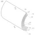
도 1은 본 발명의 한 실시예에 따른 곡면 디스플레이 패널 제조 방법에 의해 제작된 곡면 디스플레이 패널의 개략적인 사시도이다.
도 2는 도 1의 Ⅱ-Ⅱ 선을 따라 절개한 단면도이다.
도 3은 도 1의 Ⅲ-Ⅲ 선을 따라 절개한 단면도이다.
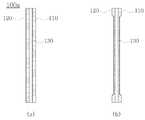
도 4는 본 발명의 한 실시예에 따른 곡면 디스플레이 패널 제조 방법에 있어서 제1 단계를 나타내는 측단면도이다.
도 5는 본 발명의 한 실시예에 따른 곡면 디스플레이 패널 제조 방법에 있어서 제2 단계를 나타내는 측단면도이다.
도 6은 본 발명의 한 실시예에 따른 곡면 디스플레이 패널 제조 방법에 있어서 제3 단계를 나타내는 측단면도이다.
도 7은 본 발명의 한 실시예에 따른 곡면 디스플레이 패널 제조 방법에 있어서 제4 단계를 나타내는 측단면도이다.
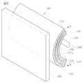
도 8은 본 발명의 다른 실시예에 따른 곡면 디스플레이 패널 제조 방법에 의해 제작된 곡면 디스플레이 패널의 개략적인 측단면도이다.
도 9는 본 발명의 한 실시예에 따른 다중 영상 표시 장치의 개략적인 사시도이다.
도 10은 도 9의 Ⅹ-Ⅹ 선을 따라 절개한 단면도이다.1 is a schematic perspective view of a curved display panel manufactured by a method of manufacturing a curved display panel according to an embodiment of the present invention.
FIG. 2 is a cross-sectional view taken along the line II-II of FIG. 1.
3 is a cross-sectional view taken along the line III-III of FIG. 1.
4 is a side cross-sectional view showing a first step in the method for manufacturing a curved display panel according to an embodiment of the present invention.
5 is a side cross-sectional view illustrating a second step in the method for manufacturing a curved display panel according to an embodiment of the present invention.
6 is a side cross-sectional view illustrating a third step in the method for manufacturing a curved display panel according to an embodiment of the present invention.
7 is a side cross-sectional view illustrating a fourth step in the method of manufacturing a curved display panel according to an embodiment of the present invention.
8 is a schematic side cross-sectional view of a curved display panel manufactured by the method for manufacturing a curved display panel according to another embodiment of the present invention.
9 is a schematic perspective view of a multi-image display device according to an exemplary embodiment.
10 is a cross-sectional view taken along the line VII-VII of FIG. 9.
이하에서 본 발명의 실시예를 첨부된 도면을 참조로 상세히 설명한다.Hereinafter, embodiments of the present invention will be described in detail with reference to the accompanying drawings.
도 1은 본 발명의 한 실시예에 따른 곡면 디스플레이 패널 제조 방법에 의해 제작된 곡면 디스플레이 패널의 개략적인 사시도이다.1 is a schematic perspective view of a curved display panel manufactured by a method of manufacturing a curved display panel according to an embodiment of the present invention.
도 2는 도 1의 Ⅱ-Ⅱ 선을 따라 절개한 단면도이고, 도 3은 도 1의 Ⅲ-Ⅲ 선을 따라 절개한 단면도이다.2 is a cross-sectional view taken along the line II-II of FIG. 1, and FIG. 3 is a cross-sectional view taken along the line III-III of FIG. 1.
도 4 내지 도 7은 본 발명의 한 실시예에 따른 곡면 디스플레이 패널 제조 방법에 있어서 제1 단계 내지 제4 단계를 각각 나타내는 측단면도이다.4 to 7 are side cross-sectional views illustrating first to fourth steps in the curved display panel manufacturing method according to the exemplary embodiment of the present invention.
도 1 내지 도 7에 도시된 바와 같이, 본 발명의 한 실시예에 따른 곡면 디스플레이 패널 제조 방법은 서로 마주하는 제1 기판(110)과 제2 기판(120)을 포함하는 평면 디스플레이 패널(100a)(도 4 참조)을 이용하여 원하는 곡면 형태의 디스플레이 패널을 제조하는 곡면 디스플레이 패널 제조 방법이다.1 to 7, a method of manufacturing a curved display panel according to an exemplary embodiment of the present invention includes a
여기서 평면 디스플레이 패널은 LCD 패널, 유기 전계발광 패널 등이 될 수 있다. 이때, LCD 패널의 경우에는 기판 사이에 액정층이 존재하고, 유기 전계발광 패널의 경우에는 기판 사이에 유기 발광층이 존재할 수 있다.The flat display panel may be an LCD panel, an organic electroluminescent panel, or the like. In this case, in the case of the LCD panel, the liquid crystal layer may be present between the substrates, and in the case of the organic electroluminescent panel, the organic light emitting layer may be present between the substrates.
예시적으로, 평면 디스플레이 패널(100a)은 유리로 형성되며 서로 마주하는 제1 기판(110)과 제2 기판(120), 그리고 제1 기판(110)과 제2 기판(120) 사이에 형성되는 액정층(130)을 포함하는 평면 형태의 액정 패널, 즉 평면 LCD 패널이 될 수 있다. 이하에서는 평면 디스플레이 패널(100a)을 주로 평면 형태의 액정 패널로 간주하여 설명을 진행한다. 다만 상술한 바와 같이 평면 디스플레이 패널(100a)이 평면 액정 패널에만 한정되는 것은 아니다.In exemplary embodiments, the flat
이때 제1 기판(110)은 박막 트랜지스터 기판(thin film transistor array panel)이라고도 불리며, 제2 기판(120)은 컬러 필터 기판(color filter array panel)이라고도 불릴 수 있다.In this case, the
한편, 도면에는 도시되지 않았으나, 두 기판(110, 120)의 가장자리에는 두 기판(110, 120)을 결합시키기 위한 물질로 이루어지고 액정이 채워지는 공간을 형성하는 밀봉재가 배치될 수 있으며, 이러한 밀봉재에 의해 채워진 액정이 새는 것을 방지할 수 있다.On the other hand, although not shown in the figure, a sealing material made of a material for bonding the two substrates (110, 120) and forming a space in which the liquid crystal is filled may be disposed at the edges of the two substrates (110, 120), such a sealing material The liquid crystal filled by can be prevented from leaking.
이하에서 첨부된 도 4 내지 도 7을 참조하여 본 발명의 한 실시예에 따른 곡면 형태를 가지는 디스플레이 패널을 제조하는 곡면 디스플레이 패널 제조 방법을 단계적으로 설명한다.Hereinafter, a method of manufacturing a curved display panel for manufacturing a display panel having a curved shape according to an embodiment of the present invention will be described with reference to FIGS. 4 to 7.
본 발명의 한 실시예에 따른 곡면 디스플레이 패널 제조 방법은 제1 기판(110)과 제2 기판(120)의 두께가 미리 설정된 두께로 감소되도록 외측 일부를 각각 깎아내는 단계(도 4의 (a)에서 (b)), 평면 디스플레이 패널(100a)을 원하는 곡면 형태로 휘는 단계(도 5의 (a)에서 (b)), 원하는 곡면 형태에 맞게 미리 제조된 제1 가이드 부재(140)를 제1 기판(110)의 깎아진 외측 면에 미리 설정된 간격을 두고 부착하고, 원하는 곡면 형태에 맞게 미리 제조된 제2 가이드 부재(150)를 제2 기판(120)의 깎아진 외측 면에 미리 설정된 간격을 두고 부착하는 단계(도 6), 그리고 제1 가이드 부재(140)와 제1 기판(110) 사이의 공간, 그리고 제2 가이드 부재(150)와 제2 기판(120) 사이의 공간에 광 투과성 보강 층(160)을 각각 형성하는 단계(도 7)를 포함한다.According to an exemplary embodiment of the present invention, a method of manufacturing a curved display panel may include cutting a portion of the outer portion such that the thicknesses of the
이때 외측 일부를 깎아내는 단계(도 4의 (a)에서 (b))에서 제1 기판(110)과 제2 기판(120)을 깎아내는 방법은 종래에 알려진 임의의 방법일 수 있다. 예를 들면, 기계적 연마 방식일 수도 있고 에칭(etching)액을 이용한 에칭 방식일 수도 있다.At this time, the method of cutting the
또한 제1 기판(110)과 제2 기판(120)의 외측 일부를 깎아낼 때, 기판의 최상단 및 최하단은 깎아내지 않는 것이 바람직하다. 디스플레이 패널을 구동시키기 위한 드라이버 및 각종 회로 소자가 부착된 PCB(Printed Circuit Board)를 포함한 구동 회로부가 기판의 최상단 또는 최하단에 연결될 수 있기 때문이다. 또한 기판의 최상단 및 최하단을 깎아내지 않음으로써, 기판의 최상단 및 최하단 부분이 제1 가이드 부재(140) 및 제2 가이드 부재(150)를 제1 기판(110) 및 제2 기판(120)의 외측 면에 미리 설정된 간격을 두고 부착함에 있어서의 가이드 역할을 할 수 있다.In addition, when scraping out part of the outer side of the 1st board |
그리고 원하는 곡면 형태는 도 1 내지 도 3에 도시된 바와 같이, 괄호 곡면 형태 또는 변곡점이 없는 곡면 형태가 될 수도 있고, S자 곡면 형태 또는 하나 이상의 변곡점이 있는 곡면 형태가 될 수도 있다. 즉 원하는 곡면 형태는 필요에 따라 본 발명의 한 실시예와 다르게 변경이 가능하다.1 to 3, the desired curved shape may be a curved shape without parenthesis curved shape or an inflection point, or may be an S-shaped curved shape or a curved shape having one or more inflection points. That is, the desired curved shape can be changed differently from one embodiment of the present invention as needed.
또한 외측 일부를 깎아내는 단계(도 4의 (a)에서 (b))에서의 미리 설정된 두께는 50 내지 200㎛에 속하는 값일 수 있다.In addition, the predetermined thickness in the step of scraping off the outer part ((a) to (b) of FIG. 4) may be a value belonging to 50 to 200 μm.
제1 기판(110)과 제2 기판(120)의 깎아진 후의 두께가 50㎛보다 작거나 200㎛보다 크면 휘는 과정에서 부서지거나 잘 휘어지지 않는 문제점이 있다. 즉 제1 기판(110)과 제2 기판(120)의 깎아진 후의 두께가 50 내지 200㎛에 속하는 값으로 하는 것은 깎아진 제1 기판(110)과 제2 기판(120)이 부서지지 않으면서 휘어질 수 있도록 하기 위함이다.If the thickness after the
원하는 곡면 형태로 휘는 단계(도 5의 (a)에서 (b))에서 평면 디스플레이 패널(100a)을 원하는 곡면 형태로 휘더라도 이를 휘어진 상태로 유지하기 위해서는 제1 기판(110)과 제2 기판(120)의 외측 면에 광 투과성 보강 층(160)이 형성되도록 하는 것이 필요하다.Even if the
이러한 광 투과성 보강 층(160)이 안정적으로 형성되도록 하기 위해서는 평면 디스플레이 패널(100a)을 휘어진 상태로 유지하는 제1 가이드 부재(140) 및 제2 가이드 부재(150)가 먼저 제1 기판(110) 및 제2 기판(120)의 외측에 각각 부착되어야 하며, 이것이 가이드 부재를 부착하는 단계(도 6)이다.In order to stably form the light
이때, 제1 가이드 부재(140) 및 제2 가이드 부재(150)는 유리, 합성수지 등 투명 또는 반투명 재질로 형성되는 기판일 수 있고, 광학성 투명 접착제(OCA, Optically clear adhesive) 등으로 제1 기판(110)과 제2 기판(120)의 외측 면에 접착될 수 있다.In this case, the
다만 제1 가이드 부재(140)와 제1 기판(110) 사이 및 제2 가이드 부재(150)와 제2 기판(120) 사이에 광 투과성 보강 층(160)이 형성될 수 있는 공간을 마련하기 위해서, 제1 가이드 부재(140) 및 제2 가이드 부재(150)는 제1 기판(110) 및 제2 기판(120)과 각각 미리 설정된 간격을 두고 부착됨이 바람직하다.However, to provide a space in which the light
이때, 미리 설정된 간격이라 함은 제1 기판(110) 또는 제2 기판(120)의 외측 일부가 깎아진 두께만큼의 간격이 될 수 있다. 또한 광 투과성 보강 층(160)이 형성될 수 있는 충분한 간격이고, 곡면 가공 시에 발생하는 응력이 광 투과성 보강 층(160)에 의해 분산 또는 흡수될 수 있는 양이 채워질 수 있는 간격으로 함이 바람직하다.In this case, the predetermined interval may be an interval equal to the thickness of the outer portion of the
그리고 광 투과성 보강 층(160)을 형성하는 단계(도 7)는 미리 설정된 간격을 둔 공간에 광 투과성 보강 층(160)이 형성되도록 하기 위해, 주입구(181a)를 통해 광 투과성 보강 물질(161)을 투입하는 단계이다. 즉 제1 가이드 부재(140)와 제2 가이드 부재(150)를 통해 제1 기판(110)과 제2 기판(120)을 휘어진 형태로 유지하는 상태에서, 그 외측 면에 액상의 광 투과성 보강 물질(161)을 입힌 후 이를 굳혀서 광 투과성 보강 층(160)을 형성할 수 있다.In the forming of the light transmissive reinforcement layer 160 (FIG. 7), the light
여기서, 광 투과성 보강 물질(161)은 빛의 투과가 가능한 보강 층을 형성할 수 있는 물질을 의미하며, 이를테면 투명 고분자 물질이나 유리 본딩(bonding) 등이 될 수 있다. 이에 따라 광 투과성 보강 층(160)은 투명 고분자 층이나 유리 본딩 층 등이 될 수 있다. 또한 투명 고분자 물질의 경우 투명 UV 레진 등 투명 또는 반투명한 임의의 고분자일 수 있다.Here, the light
또한 광 투과성 보강 층(160)은 광이 완전히 투과되도록 투명하게 형성될 수 있고, 필요에 따라서는 광이 일정량만 투과되도록 반투명하게 형성될 수도 있다.In addition, the light
광 투과성 보강 물질(161)이 굳는 과정에서 제1 기판(110) 및 제2 기판(120)의 외측 면과 접착되므로 광 투과성 보강 층(160)이 형성되고 나면 제1 기판(110), 제2 기판(120), 그리고 광 투과성 보강 층(160)이 원하는 곡면 형태를 유지할 수 있게 된다.Since the light
제1 기판(110)과 제2 기판(120)의 외측 일부를 깎아내는 가공 후 곡면 형태로 휘면, 기판의 두께가 얇아져서 휘어지지만 응력을 받게 된다. 도 5를 참고하면, 제1 기판(110)의 내측과 제2 기판(120)의 외측은 인장응력을 받게 되고, 제1 기판(110)의 외측과 제2 기판(120)의 내측은 압축응력을 받게 된다. 이때 도 7과 같이 광 투과성 보강 물질(161)이 투입되어 경화되면, 광 투과성 보강 물질(161)은 제1 기판(110)과 제2 기판(120)의 외측 면에 접착되어 광 투과성 보강 층(160)을 형성하면서 기판에 발생한 응력을 분산 또는 흡수하는 역할을 할 수 있다.When the outer substrates of the
상술한 단계를 거쳐, 제1 기판(110)과 제2 기판(120)의 외측 일부를 깎아서 두께를 얇게 한 후 원하는 곡면 형태로 휜 상태에서 그 외측 면에 가이드 기판(140, 150)을 부착하고 광 투과성 보강 층(160)을 형성함으로써, 제1 기판(110)과 제2 기판(120)이 원하는 곡면 형태를 유지할 수 있다.Through the above-described steps, by cutting the outer portion of the
또한 본 발명의 한 실시예에 따른 곡면 디스플레이 패널 제조 방법은 제1 가이드 부재(140) 및 제2 가이드 부재(150)의 외측면 중 하나 이상에 편광판(170)(polarizer)을 부착하는 단계를 더 포함할 수 있다.In addition, the curved display panel manufacturing method according to an embodiment of the present invention further comprises the step of attaching a polarizer 170 (polarizer) to at least one of the outer surface of the
도 2, 도 3, 그리고 도 6에 도시된 바와 같이, 편광판(170)은 제1 가이드 부재(140) 및 제2 가이드 부재(150)의 외측에 각각 부착되거나, 제1 가이드 부재(140) 및 제2 가이드 부재(150) 중 하나의 외측에만 부착될 수 있다.2, 3, and 6, the
제1 가이드 부재(140) 및 제2 가이드 부재(150)는 유리(glass) 또는 아크릴(PMMA, PolyMethly MethAcrylate) 재질일 수 있다.The
이상에서 가이드 부재(140, 150)가 제1 기판(110)과 제2 기판(120)의 외측 면에 각각 부착되고 가이드 부재(140, 150)와 제1 기판(110) 및 제2 기판(120) 사이의 공간에 광 투과성 보강층(160)이 각각 형성되는 경우가 설명되었으나, 본 발명이 속하는 기술분야에서 통상의 지식을 가진 자가 알 수 있듯이 가이드 부재는 제1 기판(110)과 제2 기판(120)의 외측면 중 어느 하나에만 부착되고 광 투과성 보강층(160)도 가이드 부재와 제1 기판(110)과 제2 기판(120)의 외측면 중 어느 하나 사이에만 형성될 수도 있다. 이에 대한 별도의 설명은 생략한다.In the above description, the
도 8은 본 발명의 다른 실시예에 따른 곡면 디스플레이 패널 제조 방법에 의해 제작된 곡면 디스플레이 패널의 개략적인 측단면도이다.8 is a schematic side cross-sectional view of a curved display panel manufactured by the method for manufacturing a curved display panel according to another embodiment of the present invention.
또한 제1 가이드 부재(140) 및 제2 가이드 부재(150)는 편광판일 수 있다.In addition, the
본 발명의 다른 실시예에 따른 곡면 디스플레이 패널 제조 방법 및 본 발명의 다른 실시예에 따른 곡면 디스플레이 패널(100)에 있어서는, 도 8에 나타난 바와 같이, 제 1 가이드 기판(140) 및 제2 가이드 부재(150)는 유리 또는 아크릴 재질의 기판 구성을 생략하고 그 외측에 부착되던 편광판(170)만으로 주요 구성이 이루어질 수 있다.In the curved display panel manufacturing method according to another embodiment of the present invention and the
제1 가이드 부재(140) 및 제2 가이드 부재(150)는 미리 설정된 간격을 유지하기 위한 스페이서(180)를 포함할 수 있다.The
즉 본 발명의 한 실시예에 따른 곡면 디스플레이 패널 제조 방법의 가이드 부재를 부착하는 단계(도 6)에 있어서, 제1 가이드 부재(140) 및 제2 가이드 부재(150)가 제1 기판(110) 및 제2 기판(120)과 각각 미리 설정된 간격을 두고 부착되도록 하기 위해서, 도 3에 도시된 바와 같이, 미리 설정된 간격을 유지하기 위한 스페이서(180)가 제1 가이드 부재(140) 및 제2 가이드 부재(150)의 내측에 부착될 수 있다.That is, in the attaching of the guide member (FIG. 6) of the method of manufacturing the curved display panel according to the exemplary embodiment of the present invention, the
또한 스페이서(180)는 광 투과성 보강 층(160)의 형성 시 광 투과성 보강 층(160)의 형상이 유지되도록 제1 가이드 부재(140) 및 제2 가이드 부재(150) 각각의 측면 내측에 배치되는 측면 스페이서(181)를 포함할 수 있다.In addition, the
본 발명의 한 실시예에 따른 곡면 디스플레이 패널 제조 방법의 광 투과성 보강 층을 형성하는 단계(도 7)에 있어서, 광 투과성 보강 물질(161)을 미리 설정된 간격을 둔 공간에 투입하여 광 투과성 보강 층(160)을 형성시킬 때, 광 투과성 보강 물질(161)이 경화되기 전에는 광 투과성 보강 층(160)의 형상이 유지될 수가 없다. 따라서 광 투과성 보강 층(160)의 형상이 유지되도록 하기 위해서, 도 2, 도 6 그리고 도 7에 나타난 바와 같이, 제1 가이드 부재(140) 및 제2 가이드 부재(150) 각각의 측면 내측에 측면 스페이서(181)를 배치하여 광 투과성 보강 물질(161)이 경화되기 전에 측면으로 새어나가는 것을 방지할 수 있다.In the step of forming the light transmitting reinforcing layer of the curved display panel manufacturing method according to an embodiment of the present invention (FIG. 7), the light
즉 도 3에 나타난 스페이서(180)는 미리 설정된 간격을 둔 공간 내부에 배치되는 간격 유지 부재이고, 도 2, 도 6 그리고 도 7에 나타난 측면 스페이서(181)는 미리 설정된 간격을 둔 공간의 양 측면에 배치되어 간격 유지의 역할과 함께 광 투과성 보강 층(160)의 형상을 유지하는 역할도 하는 간격 및 형상 유지 부재가 된다.That is, the
또한 도 2, 도 6 그리고 도 7에 도시된 바와 같이, 측면 스페이서(181)는 광 투과성 보강 물질(161)의 주입구(181a)를 포함할 수 있다. 도면에는 나타나지 않았으나, 주입구(181a)를 통해 광 투과성 보강 물질(161)이 투입된 후 광 투과성 보강 층(160)의 안정적인 형성을 위해 주입구(181a)는 폐쇄될 수 있다.Also, as shown in FIGS. 2, 6, and 7, the
이와 같이, 통상의 디스플레이 패널의 제1 기판(110)과 제2 기판(120)의 외측 일부를 제거하여 두께를 얇게 한 후 이를 휜 상태에서 가이드 기판(140, 150)을 부착하고 광 투과성 보강 층(160)을 형성하여 곡면 형태가 유지되도록 함으로써, 간단한 방법으로 곡면 형태를 가지는 휘어진 디스플레이 패널을 제조할 수 있다.As described above, the outer substrates of the
또한 상기한 과제를 달성하기 위한 본 발명의 한 실시예에 따른 곡면 디스플레이 패널(100)은 상술한 본 발명의 한 실시예에 따른 곡면 디스플레이 패널 제조 방법에 의해 제조된다.In addition, the
한편, 도 9는 본 발명의 한 실시예에 따른 다중 영상 표시 장치의 개략적인 사시도이고, 도 10은 도 9의 Ⅹ-Ⅹ 선을 따라 절개한 단면도이다.9 is a schematic perspective view of a multi-image display device according to an exemplary embodiment, and FIG. 10 is a cross-sectional view taken along the line VII-VII of FIG. 9.
상기한 과제를 달성하기 위한 본 발명의 한 실시예에 따른 다층 영상 표시 장치(200)는 다층의 이차원 이미지를 중첩하여 깊이를 가지는 다층 이미지를 구현하기 위한 다층 영상 표시 장치로서, 본 발명의 한 실시예에 따른 곡면 디스플레이 패널 제조 방법에 의해 제조된 곡면 디스플레이 패널(100), 그리고 곡면 디스플레이 패널(100)과 전후 방향으로 중첩되도록 곡면 디스플레이 패널(100)의 앞에 배치되는 평면 디스플레이 패널(210)을 포함한다.The multi-layer
도 9 및 도 10에 도시된 바와 같이, 평면 디스플레이 패널(210)과 곡면 디스플레이 패널(100)은 앞에서 볼 때 서로 포개져 보이도록 평면 디스플레이 패널(210)의 뒤에 곡면 디스플레이 패널(100)이 배치된다. 이때 평면 디스플레이 패널(210)과 곡면 디스플레이 패널(100)에서 구현된 영상이 깊이를 가지고 서로 중첩되도록 평면 디스플레이 패널(210)과 곡면 디스플레이 패널(100)은 약간 이격된 상태로 고정될 수 있다.9 and 10, the
또한 도 9 및 도 10에는 광원(220)만이 추가적으로 도시되어 있으나, 본 발명의 한 실시예에 따른 다층 영상 표시 장치(200)에는 백라이트 유닛(backlight unit), 광학 시트 등 통상의 디스플레이 표시 장치를 구현하기 위한 각종 부품들이 포함될 수 있다.In addition, although only the
그리고 평면 디스플레이 패널(210)은 종래에 알려진 액정 패널로 구현될 수 있다. 예를 들어, 평면 디스플레이 패널(210)은 서로 마주하도록 배치되는 한 쌍의 투명한 기판과 그 사이에 밀봉되는 액정층을 포함할 수 있으며, 액정층을 구동하기 위한 각종 전극을 포함할 수 있다.The flat
도면에는 평면 디스플레이 패널(210)과 곡면 디스플레이 패널(100)을 서로 고정하는 프레임(frame) 등은 생략되었다.In the drawing, a frame for fixing the
또한 평면 디스플레이 패널(210)은 뒤에 있는 곡면 디스플레이 패널(100)에서 구현된 영상이 전면에서 보일 수 있게 선택적으로 투명한 상태가 되도록 형성될 수 있다.In addition, the flat
기존의 다층 이미지를 구현을 위한 복수의 평면 액정 디스플레이 패널의 중첩 방식의 경우, 중첩된 평면 액정 디스플레이 패널 사이의 간섭에 의해 나뭇결 모양이나 물결 모양 등의 노이즈(간섭무늬)가 발생하는 문제점이 있었다. 이와 같은 노이즈의 발생을 방지하기 위해, 두 개의 평면 액정 디스플레이 패널 사이에 광을 약간 확산하는 확산층(diffuse layer)을 배치하는 기술이 소개된 바 있으나, 두 개의 액정 디스플레이 패널 사이에 확산층을 배치하는 경우 조립 과정이 번거롭고 생산성이 저하된다.In the case of the overlapping method of a plurality of flat liquid crystal display panels for implementing a conventional multilayer image, there is a problem in that noise (interference patterns) such as wood grains or wavy shapes is generated by interference between the overlapping flat liquid crystal display panels. In order to prevent the occurrence of such noise, a technique of disposing a diffusion layer slightly diffusing light between two flat liquid crystal display panels has been introduced, but in the case of disposing a diffusion layer between two liquid crystal display panels The assembly process is cumbersome and the productivity is lowered.
이에 대해 본 발명의 한 실시예에 따른 다층 영상 표시 장치(200)는, 도 9 및 도 10에 나타난 바와 같이, 두 개의 평면 디스플레이 패널 중 뒤에 위치한 평면 디스플레이 패널을 본 발명의 한 실시예에 따른 곡면 디스플레이 패널(100)로 대체하여, 간섭무늬의 문제점을 해결하면서 조립 과정도 간소화하고자 하였다.In contrast, as illustrated in FIGS. 9 and 10, the multilayer
즉 기존의 다층 영상 표시 장치의 경우, 중첩된 두 개의 평면 액정 표시 장치의 배치 위치에 따른 양 픽셀 패턴(pixel pattern) 사이의 원근 차이 등의 미세한 상이함으로 인해 간섭무늬가 발생하게 된다. 이에 반해 곡면 디스플레이 패널(100)은 픽셀 패턴이 곡면 형태에 따라 휘어져 왜곡되므로, 평면 디스플레이 패널(210)과 곡면 디스플레이 패널(100)이 중첩되더라도 양 픽셀 패턴의 차이가 미세한 정도 이상으로 상이하게 되어 간섭무늬의 발생이 방지될 수 있다.That is, in the conventional multilayer image display device, an interference pattern is generated due to a minute difference such as a perspective difference between pixel patterns according to the arrangement positions of two superimposed flat liquid crystal display devices. In contrast, since the
두 개의 액정 디스플레이 패널 사이에 광을 약간 확산하는 확산층(diffuse layer)을 배치하는 경우에는 미세하게 상이한 픽셀 패턴의 중첩 자체를 방지하는 것은 아니므로 간섭무늬의 발생을 약화시키는 정도의 효과가 있다. 그러나 본 발명의 경우 두 픽셀 패턴의 미세하게 상이한 중첩이 없어지므로 간섭무늬의 발생이 더욱 방지될 수 있다.In the case of disposing a diffuser layer that slightly diffuses light between two liquid crystal display panels, there is an effect of weakening the occurrence of interference fringes because it does not prevent the superposition of minutely different pixel patterns. However, in the case of the present invention, since the overlapping of the two pixel patterns is slightly different, the generation of the interference fringe can be further prevented.
이와 같이, 곡면 디스플레이 패널(100)을 다층 영상 표시 장치의 후면 디스플레이로 사용함으로써, 상이한 픽셀 패턴의 간섭에 의한 간섭무늬의 발생(모아레 현상)을 방지할 수 있고, 별도의 확산층을 형성하지 않아도 되므로 다층 영상 표시 장치의 조립 공정이 보다 간단해질 수 있다.As such, by using the
이상에서 본 발명의 실시예를 설명하였으나, 본 발명의 권리범위는 이에 한정되지 아니하며 본 발명의 실시예로부터 본 발명이 속하는 기술분야에서 통상의 지식을 가진 자에 의해 용이하게 변경되어 균등한 것으로 인정되는 범위의 모든 변경 및 수정을 포함한다.While the present invention has been particularly shown and described with reference to exemplary embodiments, it is to be understood that the invention is not limited to the disclosed exemplary embodiments, but, on the contrary, And all changes and modifications to the scope of the invention.
110: 제1 기판
120: 제2 기판
140: 제1 가이드 부재
150: 제2 가이드 부재
160: 광 투과성 보강층
170: 편광판
180: 스페이서110: first substrate
120: second substrate
140: first guide member
150: second guide member
160: light transmissive reinforcing layer
170: polarizer
180: spacer
Claims (10)
Translated fromKorean상기 제1 기판과 상기 제2 기판의 두께가 미리 설정된 두께로 감소되도록 외측 일부를 각각 깎아내는 단계,
상기 외측 일부가 깎아진 평면 디스플레이 패널을 상기 원하는 곡면 형태로 휘는 단계,
상기 원하는 곡면 형태에 맞게 미리 제조된 제1 가이드 부재를 상기 제1 기판의 깎아진 외측 면에 미리 설정된 간격을 두고 부착하고, 상기 원하는 곡면 형태에 맞게 미리 제조된 제2 가이드 부재를 상기 제2 기판의 깎아진 외측 면에 미리 설정된 간격을 두고 부착하는 단계, 그리고
상기 제1 가이드 부재와 상기 제1 기판 사이의 공간, 그리고 상기 제2 가이드 부재와 상기 제2 기판 사이의 공간에, 상기 제1 기판과 상기 제2 기판이 상기 원하는 곡면 형태를 유지할 수 있도록 하는 힘을 제공하는 광 투과성 보강 층을 각각 형성하는 단계를 포함하고,
상기 광 투과성 보강 층은 액상의 광 투과성 보강 물질을 경화시켜 형성되는 곡면 디스플레이 패널 제조 방법.A curved display panel manufacturing method of manufacturing a display panel having a desired curved shape using a flat panel display panel including a first substrate and a second substrate facing each other,
Slicing the outer portion so that the thickness of the first substrate and the second substrate is reduced to a predetermined thickness, respectively,
Bending the flat panel display having the outer portion cut off into the desired curved shape;
The first guide member manufactured according to the desired curved shape is attached to the cut outer surface of the first substrate at a predetermined interval, and the second guide member manufactured according to the desired curved shape is attached to the second substrate. Attaching at predetermined intervals to the sheared outer surface of the, and
A force that allows the first substrate and the second substrate to maintain the desired curved shape in a space between the first guide member and the first substrate and a space between the second guide member and the second substrate Each forming a light transmissive reinforcing layer providing a,
The light transmissive reinforcing layer is formed by curing a light transmissive reinforcing material liquid.
상기 미리 설정된 두께는 50 내지 200㎛에 속하는 값인 곡면 디스플레이 패널 제조 방법.In claim 1,
The predetermined thickness is a curved display panel manufacturing method of the value belonging to 50 to 200㎛.
상기 제1 가이드 부재 및 상기 제2 가이드 부재의 외측면 중 하나 이상에 편광판(polarizer)을 부착하는 단계를 더 포함하는 곡면 디스플레이 패널 제조 방법.In claim 1,
And attaching a polarizer to at least one of an outer surface of the first guide member and the second guide member.
상기 제1 가이드 부재 및 상기 제2 가이드 부재는 유리(glass) 또는 아크릴(PMMA, PolyMethly MethAcrylate) 재질인 곡면 디스플레이 패널 제조 방법.In claim 1,
The first guide member and the second guide member is a glass or acrylic (PMMA, PolyMethly Meth Acrylate) material manufacturing method of a curved display panel.
상기 제1 가이드 부재 및 상기 제2 가이드 부재는 편광판인 곡면 디스플레이 패널 제조 방법.In claim 1,
And the first guide member and the second guide member are polarizing plates.
상기 제1 기판과 상기 제2 기판의 두께가 미리 설정된 두께로 감소되도록 외측 일부를 각각 깎아내는 단계,
상기 외측 일부가 깎아진 평면 디스플레이 패널을 상기 원하는 곡면 형태로 휘는 단계,
상기 원하는 곡면 형태에 맞게 미리 제조된 가이드 부재를 상기 제1 기판 및 상기 제2 기판이 상기 곡면 형태로 휘어진 상태에서 상기 제1 기판 및 상기 제2 기판의 깎아진 외측면 중 하나에 미리 설정된 간격을 두고 부착하는 단계, 그리고
상기 가이드 부재와 상기 제1 기판 또는 상기 제2 기판 사이의 공간에 상기 제1 기판과 상기 제2 기판이 상기 원하는 곡면 형태를 유지할 수 있도록 하는 힘을 제공하는 광 투과성 보강 층을 형성하는 단계를 포함하고,
상기 광 투과성 보강 층은 액상의 광 투과성 보강 물질을 경화시켜 형성되는 곡면 디스플레이 패널 제조 방법.A curved display panel manufacturing method of manufacturing a display panel having a desired curved shape using a flat panel display panel including a first substrate and a second substrate facing each other,
Slicing the outer portion so that the thickness of the first substrate and the second substrate is reduced to a predetermined thickness, respectively,
Bending the flat panel display having the outer portion cut off into the desired curved shape;
The guide member pre-fabricated according to the desired curved shape is pre-set to one of the outer side surfaces of the first substrate and the second substrate while the first substrate and the second substrate are bent in the curved shape. Placing and attaching, and
Forming a light transmissive reinforcing layer in the space between the guide member and the first substrate or the second substrate to provide a force that allows the first substrate and the second substrate to maintain the desired curved shape. and,
The light transmissive reinforcing layer is formed by curing a light transmissive reinforcing material liquid.
상기 가이드 부재의 외측면에 편광판(polarizer)을 부착하는 단계를 더 포함하는 곡면 디스플레이 패널 제조 방법.The method of claim 6,
And attaching a polarizer to an outer surface of the guide member.
상기 가이드 부재는 편광판인 곡면 디스플레이 패널 제조 방법.The method of claim 6,
And said guide member is a polarizing plate.
Priority Applications (1)
| Application Number | Priority Date | Filing Date | Title |
|---|---|---|---|
| KR1020110137952AKR101268471B1 (en) | 2011-12-20 | 2011-12-20 | Method for forming display panel with curved shape, display panel with curved shape using the method, and multi-layer image display device using the display panel |
Applications Claiming Priority (1)
| Application Number | Priority Date | Filing Date | Title |
|---|---|---|---|
| KR1020110137952AKR101268471B1 (en) | 2011-12-20 | 2011-12-20 | Method for forming display panel with curved shape, display panel with curved shape using the method, and multi-layer image display device using the display panel |
Related Parent Applications (1)
| Application Number | Title | Priority Date | Filing Date |
|---|---|---|---|
| KR1020100019585ADivisionKR101113289B1 (en) | 2010-03-04 | 2010-03-04 | Method for forming display panel with curved shape, display panel with curved shape using the method, and multi-layer image display device using the display panel |
Publications (2)
| Publication Number | Publication Date |
|---|---|
| KR20120013265A KR20120013265A (en) | 2012-02-14 |
| KR101268471B1true KR101268471B1 (en) | 2013-06-04 |
Family
ID=45836910
Family Applications (1)
| Application Number | Title | Priority Date | Filing Date |
|---|---|---|---|
| KR1020110137952AExpired - Fee RelatedKR101268471B1 (en) | 2011-12-20 | 2011-12-20 | Method for forming display panel with curved shape, display panel with curved shape using the method, and multi-layer image display device using the display panel |
Country Status (1)
| Country | Link |
|---|---|
| KR (1) | KR101268471B1 (en) |
Cited By (63)
| Publication number | Priority date | Publication date | Assignee | Title |
|---|---|---|---|---|
| USD812148S1 (en) | 2016-03-30 | 2018-03-06 | Bally Gaming, Inc. | Gaming machine with curved display |
| USD832358S1 (en) | 2016-09-13 | 2018-10-30 | Bally Gaming, Inc. | Gaming machine with curved display |
| USD832355S1 (en) | 2016-09-13 | 2018-10-30 | Bally Gaming, Inc. | Gaming machine with curved display |
| USD832356S1 (en) | 2016-09-13 | 2018-10-30 | Bally Gaming, Inc. | Gaming machine with curved display |
| USD832357S1 (en) | 2016-09-13 | 2018-10-30 | Bally Gaming, Inc. | Gaming machine with curved display |
| USD836164S1 (en) | 2016-09-13 | 2018-12-18 | Bally Gaming, Inc. | Curved display for a gaming machine |
| USD843460S1 (en) | 2016-09-13 | 2019-03-19 | Bally Gaming, Inc. | Gaming machine with curved display |
| USD843466S1 (en) | 2016-09-13 | 2019-03-19 | Bally Gaming, Inc. | Gaming machine with curved display |
| USD843462S1 (en) | 2016-09-13 | 2019-03-19 | Bally Gaming, Inc. | Gaming machine with curved display |
| USD843475S1 (en) | 2013-04-17 | 2019-03-19 | Bally Gaming, Inc. | Gaming machine |
| USD843464S1 (en) | 2016-09-13 | 2019-03-19 | Bally Gaming, Inc. | Gaming machine with curved display |
| USD843458S1 (en) | 2016-03-30 | 2019-03-19 | Bally Gaming, Inc. | Gaming machine with curved display |
| USD843465S1 (en) | 2016-09-13 | 2019-03-19 | Bally Gaming, Inc. | Gaming machine with curved display |
| USD843459S1 (en) | 2016-03-30 | 2019-03-19 | Bally Gaming, Inc. | Gaming machine with curved display |
| USD843480S1 (en) | 2018-06-01 | 2019-03-19 | Bally Gaming, Inc. | Gaming machine with curved display |
| USD843461S1 (en) | 2016-09-13 | 2019-03-19 | Bally Gaming, Inc. | Gaming machine with curved display |
| USD843463S1 (en) | 2016-09-13 | 2019-03-19 | Bally Gaming, Inc. | Gaming machine with curved display |
| USD843477S1 (en) | 2013-04-17 | 2019-03-19 | Bally Gaming, Inc. | Gaming machine |
| USD850537S1 (en) | 2017-09-05 | 2019-06-04 | Aristocrat Technologies Australia Pty Limited | Gaming machine |
| USD871506S1 (en) | 2016-09-13 | 2019-12-31 | Bally Gaming, Inc. | Gaming machine with curved displays |
| USD872189S1 (en) | 2018-07-24 | 2020-01-07 | Bally Gaming, Inc. | Gaming machine |
| USD872188S1 (en) | 2018-07-24 | 2020-01-07 | Bally Gaming, Inc. | Gaming machine |
| USD873921S1 (en) | 2018-07-24 | 2020-01-28 | Bally Gaming, Inc. | Gaming machine |
| USD877811S1 (en) | 2018-07-02 | 2020-03-10 | Sg Gaming, Inc. | Gaming machine |
| USD878477S1 (en) | 2018-07-02 | 2020-03-17 | Sg Gaming, Inc. | Gaming machine |
| USD880614S1 (en) | 2018-07-24 | 2020-04-07 | Sg Gaming, Inc. | Gaming machine |
| USD880612S1 (en) | 2018-07-24 | 2020-04-07 | Sg Gaming, Inc. | Gaming machine |
| USD880610S1 (en) | 2018-07-24 | 2020-04-07 | Sg Gaming, Inc. | Gaming machine |
| USD880608S1 (en) | 2018-07-24 | 2020-04-07 | Sg Gaming, Inc. | Gaming machine |
| USD880606S1 (en) | 2017-09-28 | 2020-04-07 | Sg Gaming, Inc. | Gaming terminal |
| USD880613S1 (en) | 2018-07-24 | 2020-04-07 | Sg Gaming, Inc. | Gaming machine |
| USD880615S1 (en) | 2018-07-24 | 2020-04-07 | Sg Gaming, Inc. | Gaming machine |
| USD880609S1 (en) | 2018-07-24 | 2020-04-07 | Bally Gaming, Inc. | Gaming machine with graphical user interface |
| USD880611S1 (en) | 2018-07-24 | 2020-04-07 | Sg Gaming, Inc. | Gaming machine |
| USD881284S1 (en) | 2018-07-24 | 2020-04-14 | Sg Gaming, Inc. | Gaming machine |
| USD881285S1 (en) | 2018-07-24 | 2020-04-14 | Sg Gaming, Inc. | Gaming machine |
| USD881995S1 (en) | 2018-07-24 | 2020-04-21 | Sg Gaming, Inc. | Gaming machine |
| USD882694S1 (en) | 2018-07-24 | 2020-04-28 | Sg Gaming, Inc. | Gaming machine |
| USD882700S1 (en) | 2017-04-14 | 2020-04-28 | Sg Gaming, Inc. | Gaming machine carousel display |
| USD882699S1 (en) | 2017-04-14 | 2020-04-28 | Sg Gaming, Inc. | Gaming machine carousel display |
| USD882695S1 (en) | 2018-07-24 | 2020-04-28 | Sg Gaming, Inc. | Gaming machine |
| USD883393S1 (en) | 2017-04-14 | 2020-05-05 | Sg Gaming, Inc. | Gaming machine carousel display |
| USD884079S1 (en) | 2018-07-24 | 2020-05-12 | Sg Gaming, Inc. | Gaming machine |
| USD886905S1 (en) | 2018-07-24 | 2020-06-09 | Sg Gaming, Inc. | Gaming machine |
| USD887495S1 (en) | 2018-07-24 | 2020-06-16 | Sg Gaming, Inc. | Gaming machine |
| USD889553S1 (en) | 2017-09-28 | 2020-07-07 | Sg Gaming, Inc. | Gaming terminal |
| USD889552S1 (en) | 2017-09-28 | 2020-07-07 | Sg Gaming, Inc. | Gaming terminal |
| USD894285S1 (en) | 2018-07-24 | 2020-08-25 | Sg Gaming, Inc. | Gaming machine |
| USD896313S1 (en) | 2016-03-30 | 2020-09-15 | Sg Gaming, Inc. | Gaming machine with curved display |
| USD913376S1 (en) | 2018-07-02 | 2021-03-16 | Sg Gaming, Inc. | Gaming machine |
| USD913377S1 (en) | 2018-07-02 | 2021-03-16 | Sg Gaming, Inc. | Gaming machine |
| USD915523S1 (en) | 2017-09-28 | 2021-04-06 | Sg Gaming, Inc. | Gaming terminal |
| WO2021158094A1 (en)* | 2020-02-06 | 2021-08-12 | 주식회사 토비스 | Partially curved or foldable display device and manufacturing method therefor |
| USD952753S1 (en) | 2019-10-11 | 2022-05-24 | Sg Gaming, Inc. | Gaming machine |
| USD952752S1 (en) | 2019-10-11 | 2022-05-24 | Sg Gaming, Inc. | Gaming machine |
| USD952755S1 (en) | 2019-10-11 | 2022-05-24 | Sg Gaming, Inc. | Gaming machine |
| USD952750S1 (en) | 2019-10-11 | 2022-05-24 | Sg Gaming, Inc. | Gaming machine |
| USD952754S1 (en) | 2019-10-11 | 2022-05-24 | Sg Gaming, Inc. | Gaming machine |
| USD952751S1 (en) | 2019-10-11 | 2022-05-24 | Sg Gaming, Inc. | Gaming machine |
| US11854345B2 (en) | 2019-08-30 | 2023-12-26 | Aristocrat Technologies Australia Pty Limited | Systems and methods for supplementing a wagering game |
| USD1023156S1 (en) | 2019-08-29 | 2024-04-16 | Aristocrat Technologies Australia Pty Limited | Gaming machine with stepper reel and display screen with a transitional graphical user interface |
| USD1034820S1 (en) | 2018-07-24 | 2024-07-09 | Lnw Gaming, Inc. | Gaming machine |
| USD1034821S1 (en) | 2018-07-24 | 2024-07-09 | Lnw Gaming, Inc. | Gaming machine |
Families Citing this family (4)
| Publication number | Priority date | Publication date | Assignee | Title |
|---|---|---|---|---|
| JP6607666B2 (en) | 2013-10-10 | 2019-11-20 | 三星ディスプレイ株式會社 | Window member of curved surface display device, method of manufacturing window member of curved surface display device, and curved surface display device including the same |
| KR101746650B1 (en) | 2014-09-02 | 2017-06-14 | 주식회사 토비스 | a apparatus of curved display manufacturing, and a method of curved display manufacturing |
| KR102242439B1 (en) | 2014-09-30 | 2021-04-20 | 삼성디스플레이 주식회사 | Curved liquid crystal display |
| KR101669422B1 (en) | 2015-07-24 | 2016-10-26 | 이피네트시스템즈 주식회사 | Method for manufacturing display with curved shape and display with curved shape using the method |
Citations (4)
| Publication number | Priority date | Publication date | Assignee | Title |
|---|---|---|---|---|
| JP2002214566A (en)* | 2001-01-22 | 2002-07-31 | Nippon Telegr & Teleph Corp <Ntt> | Three-dimensional display method and device |
| KR100435826B1 (en)* | 1996-10-16 | 2004-08-25 | 엘지.필립스 엘시디 주식회사 | Lcd in bent plate shape for improving viewing angle and fabricating method thereof |
| JP2006106603A (en)* | 2004-10-08 | 2006-04-20 | Toshiba Matsushita Display Technology Co Ltd | Display device |
| JP2010156784A (en) | 2008-12-26 | 2010-07-15 | Sharp Corp | Liquid crystal display apparatus |
- 2011
- 2011-12-20KRKR1020110137952Apatent/KR101268471B1/ennot_activeExpired - Fee Related
Patent Citations (4)
| Publication number | Priority date | Publication date | Assignee | Title |
|---|---|---|---|---|
| KR100435826B1 (en)* | 1996-10-16 | 2004-08-25 | 엘지.필립스 엘시디 주식회사 | Lcd in bent plate shape for improving viewing angle and fabricating method thereof |
| JP2002214566A (en)* | 2001-01-22 | 2002-07-31 | Nippon Telegr & Teleph Corp <Ntt> | Three-dimensional display method and device |
| JP2006106603A (en)* | 2004-10-08 | 2006-04-20 | Toshiba Matsushita Display Technology Co Ltd | Display device |
| JP2010156784A (en) | 2008-12-26 | 2010-07-15 | Sharp Corp | Liquid crystal display apparatus |
Cited By (110)
| Publication number | Priority date | Publication date | Assignee | Title |
|---|---|---|---|---|
| USD843478S1 (en) | 2013-04-17 | 2019-03-19 | Bally Gaming, Inc. | Gaming machine |
| USD882698S1 (en) | 2013-04-17 | 2020-04-28 | Sg Gaming, Inc. | Gaming machine |
| USD843477S1 (en) | 2013-04-17 | 2019-03-19 | Bally Gaming, Inc. | Gaming machine |
| USD843476S1 (en) | 2013-04-17 | 2019-03-19 | Bally Gaming, Inc. | Gaming machine |
| USD844062S1 (en) | 2013-04-17 | 2019-03-26 | Bally Gaming, Inc. | Gaming machine |
| USD882697S1 (en) | 2013-04-17 | 2020-04-28 | Sg Gaming, Inc. | Gaming machine |
| USD843474S1 (en) | 2013-04-17 | 2019-03-19 | Bally Gaming, Inc. | Gaming machine |
| USD882696S1 (en) | 2013-04-17 | 2020-04-28 | Sg Gaming, Inc. | Gaming machine |
| USD895019S1 (en) | 2013-04-17 | 2020-09-01 | Sg Gaming, Inc. | Gaming machine |
| USD843475S1 (en) | 2013-04-17 | 2019-03-19 | Bally Gaming, Inc. | Gaming machine |
| USD896315S1 (en) | 2016-03-30 | 2020-09-15 | Sg Gaming, Inc. | Gaming machine with curved display |
| USD812148S1 (en) | 2016-03-30 | 2018-03-06 | Bally Gaming, Inc. | Gaming machine with curved display |
| USD843458S1 (en) | 2016-03-30 | 2019-03-19 | Bally Gaming, Inc. | Gaming machine with curved display |
| USD896313S1 (en) | 2016-03-30 | 2020-09-15 | Sg Gaming, Inc. | Gaming machine with curved display |
| USD843479S1 (en) | 2016-03-30 | 2019-03-19 | Bally Gaming, Inc. | Gaming machine with curved display |
| USD910116S1 (en) | 2016-03-30 | 2021-02-09 | Sg Gaming, Inc. | Gaming machine with curved display |
| USD896312S1 (en) | 2016-03-30 | 2020-09-15 | Sg Gaming, Inc. | Gaming machine with curved display |
| USD812147S1 (en) | 2016-03-30 | 2018-03-06 | Bally Gaming, Inc. | Gaming machine with curved display |
| USD896314S1 (en) | 2016-03-30 | 2020-09-15 | Sg Gaming, Inc. | Gaming machine with curved display |
| USD843459S1 (en) | 2016-03-30 | 2019-03-19 | Bally Gaming, Inc. | Gaming machine with curved display |
| USD1055165S1 (en) | 2016-03-30 | 2024-12-24 | Lnw Gaming, Inc. | Gaming machine with curved display |
| USD819747S1 (en) | 2016-03-30 | 2018-06-05 | Bally Gaming, Inc. | Gaming machine with curved display |
| USD812146S1 (en) | 2016-03-30 | 2018-03-06 | Bally Gaming, Inc. | Gaming machine with curved display |
| USD812149S1 (en) | 2016-03-30 | 2018-03-06 | Bally Gaming, Inc. | Gaming machine with curved display |
| USD843460S1 (en) | 2016-09-13 | 2019-03-19 | Bally Gaming, Inc. | Gaming machine with curved display |
| USD843466S1 (en) | 2016-09-13 | 2019-03-19 | Bally Gaming, Inc. | Gaming machine with curved display |
| USD843461S1 (en) | 2016-09-13 | 2019-03-19 | Bally Gaming, Inc. | Gaming machine with curved display |
| USD843465S1 (en) | 2016-09-13 | 2019-03-19 | Bally Gaming, Inc. | Gaming machine with curved display |
| USD843464S1 (en) | 2016-09-13 | 2019-03-19 | Bally Gaming, Inc. | Gaming machine with curved display |
| USD843462S1 (en) | 2016-09-13 | 2019-03-19 | Bally Gaming, Inc. | Gaming machine with curved display |
| USD871506S1 (en) | 2016-09-13 | 2019-12-31 | Bally Gaming, Inc. | Gaming machine with curved displays |
| USD843463S1 (en) | 2016-09-13 | 2019-03-19 | Bally Gaming, Inc. | Gaming machine with curved display |
| USD832358S1 (en) | 2016-09-13 | 2018-10-30 | Bally Gaming, Inc. | Gaming machine with curved display |
| USD836164S1 (en) | 2016-09-13 | 2018-12-18 | Bally Gaming, Inc. | Curved display for a gaming machine |
| USD832357S1 (en) | 2016-09-13 | 2018-10-30 | Bally Gaming, Inc. | Gaming machine with curved display |
| USD832355S1 (en) | 2016-09-13 | 2018-10-30 | Bally Gaming, Inc. | Gaming machine with curved display |
| USD832356S1 (en) | 2016-09-13 | 2018-10-30 | Bally Gaming, Inc. | Gaming machine with curved display |
| USD883393S1 (en) | 2017-04-14 | 2020-05-05 | Sg Gaming, Inc. | Gaming machine carousel display |
| USD882700S1 (en) | 2017-04-14 | 2020-04-28 | Sg Gaming, Inc. | Gaming machine carousel display |
| USD882699S1 (en) | 2017-04-14 | 2020-04-28 | Sg Gaming, Inc. | Gaming machine carousel display |
| USD850537S1 (en) | 2017-09-05 | 2019-06-04 | Aristocrat Technologies Australia Pty Limited | Gaming machine |
| USD871507S1 (en) | 2017-09-05 | 2019-12-31 | Aristocrat Technologies Australia Pty Limited | Gaming machine display |
| USD898128S1 (en) | 2017-09-05 | 2020-10-06 | Aristocrat Technologies Australia Pty Limited | Gaming machine |
| USD1042647S1 (en) | 2017-09-05 | 2024-09-17 | Aristocrat Technologies Australia Pty Limited | Gaming machine |
| USD1040237S1 (en) | 2017-09-05 | 2024-08-27 | Aristocrat Technologies Australia Pty Limited | Gaming machine |
| USD1040238S1 (en) | 2017-09-05 | 2024-08-27 | Aristocrat Technologies Australia Pty Limited | Gaming machine |
| USD870820S1 (en) | 2017-09-05 | 2019-12-24 | Aristocrat Technologies Australia Pty Limited | Gaming machine display |
| USD1031854S1 (en) | 2017-09-28 | 2024-06-18 | Lnw Gaming, Inc. | Gaming terminal |
| USD915523S1 (en) | 2017-09-28 | 2021-04-06 | Sg Gaming, Inc. | Gaming terminal |
| USD880606S1 (en) | 2017-09-28 | 2020-04-07 | Sg Gaming, Inc. | Gaming terminal |
| USD1031853S1 (en) | 2017-09-28 | 2024-06-18 | Lnw Gaming, Inc. | Gaming terminal |
| USD1032728S1 (en) | 2017-09-28 | 2024-06-25 | Lnw Gaming, Inc. | Gaming terminal |
| USD1031852S1 (en) | 2017-09-28 | 2024-06-18 | Lnw Gaming, Inc. | Gaming terminal |
| USD1002738S1 (en) | 2017-09-28 | 2023-10-24 | Lnw Gaming, Inc. | Gaming terminal |
| USD1031855S1 (en) | 2017-09-28 | 2024-06-18 | Lnw Gaming, Inc. | Gaming terminal |
| USD889552S1 (en) | 2017-09-28 | 2020-07-07 | Sg Gaming, Inc. | Gaming terminal |
| USD889553S1 (en) | 2017-09-28 | 2020-07-07 | Sg Gaming, Inc. | Gaming terminal |
| USD1036553S1 (en) | 2017-09-28 | 2024-07-23 | Lnw Gaming, Inc. | Gaming terminal |
| USD843480S1 (en) | 2018-06-01 | 2019-03-19 | Bally Gaming, Inc. | Gaming machine with curved display |
| USD913376S1 (en) | 2018-07-02 | 2021-03-16 | Sg Gaming, Inc. | Gaming machine |
| USD913377S1 (en) | 2018-07-02 | 2021-03-16 | Sg Gaming, Inc. | Gaming machine |
| USD878477S1 (en) | 2018-07-02 | 2020-03-17 | Sg Gaming, Inc. | Gaming machine |
| USD877811S1 (en) | 2018-07-02 | 2020-03-10 | Sg Gaming, Inc. | Gaming machine |
| USD886905S1 (en) | 2018-07-24 | 2020-06-09 | Sg Gaming, Inc. | Gaming machine |
| USD881995S1 (en) | 2018-07-24 | 2020-04-21 | Sg Gaming, Inc. | Gaming machine |
| USD872189S1 (en) | 2018-07-24 | 2020-01-07 | Bally Gaming, Inc. | Gaming machine |
| USD873921S1 (en) | 2018-07-24 | 2020-01-28 | Bally Gaming, Inc. | Gaming machine |
| USD894285S1 (en) | 2018-07-24 | 2020-08-25 | Sg Gaming, Inc. | Gaming machine |
| USD887495S1 (en) | 2018-07-24 | 2020-06-16 | Sg Gaming, Inc. | Gaming machine |
| USD880613S1 (en) | 2018-07-24 | 2020-04-07 | Sg Gaming, Inc. | Gaming machine |
| USD884079S1 (en) | 2018-07-24 | 2020-05-12 | Sg Gaming, Inc. | Gaming machine |
| USD882695S1 (en) | 2018-07-24 | 2020-04-28 | Sg Gaming, Inc. | Gaming machine |
| USD1069922S1 (en) | 2018-07-24 | 2025-04-08 | Lnw Gaming, Inc. | Gaming machine |
| USD1068941S1 (en) | 2018-07-24 | 2025-04-01 | Lnw Gaming, Inc. | Gaming machine with graphical user interface |
| USD880615S1 (en) | 2018-07-24 | 2020-04-07 | Sg Gaming, Inc. | Gaming machine |
| USD880609S1 (en) | 2018-07-24 | 2020-04-07 | Bally Gaming, Inc. | Gaming machine with graphical user interface |
| USD880611S1 (en) | 2018-07-24 | 2020-04-07 | Sg Gaming, Inc. | Gaming machine |
| USD881284S1 (en) | 2018-07-24 | 2020-04-14 | Sg Gaming, Inc. | Gaming machine |
| USD881285S1 (en) | 2018-07-24 | 2020-04-14 | Sg Gaming, Inc. | Gaming machine |
| USD880614S1 (en) | 2018-07-24 | 2020-04-07 | Sg Gaming, Inc. | Gaming machine |
| USD1034821S1 (en) | 2018-07-24 | 2024-07-09 | Lnw Gaming, Inc. | Gaming machine |
| USD1034820S1 (en) | 2018-07-24 | 2024-07-09 | Lnw Gaming, Inc. | Gaming machine |
| USD1011431S1 (en) | 2018-07-24 | 2024-01-16 | Lnw Gaming, Inc. | Gaming machine |
| USD1011430S1 (en) | 2018-07-24 | 2024-01-16 | Lnw Gaming, Inc. | Gaming machine |
| USD1012185S1 (en) | 2018-07-24 | 2024-01-23 | Lnw Gaming, Inc. | Gaming machine |
| USD1012183S1 (en) | 2018-07-24 | 2024-01-23 | Lnw Gaming, Inc. | Gaming machine |
| USD1012186S1 (en) | 2018-07-24 | 2024-01-23 | Lnw Gaming, Inc. | Gaming machine with graphical user interface |
| USD1012184S1 (en) | 2018-07-24 | 2024-01-23 | Lnw Gaming, Inc. | Gaming machine with graphical user interface |
| USD1013044S1 (en) | 2018-07-24 | 2024-01-30 | Lnw Gaming, Inc. | Gaming machine |
| USD1018678S1 (en) | 2018-07-24 | 2024-03-19 | Lnw Gaming, Inc. | Gaming machine |
| USD1018677S1 (en) | 2018-07-24 | 2024-03-19 | Lnw Gaming, Inc. | Gaming machine |
| USD1033542S1 (en) | 2018-07-24 | 2024-07-02 | Lnw Gaming, Inc. | Gaming machine |
| USD880612S1 (en) | 2018-07-24 | 2020-04-07 | Sg Gaming, Inc. | Gaming machine |
| USD880610S1 (en) | 2018-07-24 | 2020-04-07 | Sg Gaming, Inc. | Gaming machine |
| USD880608S1 (en) | 2018-07-24 | 2020-04-07 | Sg Gaming, Inc. | Gaming machine |
| USD882694S1 (en) | 2018-07-24 | 2020-04-28 | Sg Gaming, Inc. | Gaming machine |
| USD1032721S1 (en) | 2018-07-24 | 2024-06-25 | Lnw Gaming, Inc. | Gaming machine with graphical user interface |
| USD872188S1 (en) | 2018-07-24 | 2020-01-07 | Bally Gaming, Inc. | Gaming machine |
| USD1023156S1 (en) | 2019-08-29 | 2024-04-16 | Aristocrat Technologies Australia Pty Limited | Gaming machine with stepper reel and display screen with a transitional graphical user interface |
| USD1046978S1 (en) | 2019-08-29 | 2024-10-15 | Aristocrat Technologies Australia Pty Limited | Gaming machine with stepper reel and display screen with a transitional graphical user interface |
| US11854345B2 (en) | 2019-08-30 | 2023-12-26 | Aristocrat Technologies Australia Pty Limited | Systems and methods for supplementing a wagering game |
| US12249216B2 (en) | 2019-08-30 | 2025-03-11 | Aristocrat Technologies Australia Pty Limited | Systems and methods for supplementing a wagering game |
| USD952751S1 (en) | 2019-10-11 | 2022-05-24 | Sg Gaming, Inc. | Gaming machine |
| USD952754S1 (en) | 2019-10-11 | 2022-05-24 | Sg Gaming, Inc. | Gaming machine |
| USD952750S1 (en) | 2019-10-11 | 2022-05-24 | Sg Gaming, Inc. | Gaming machine |
| USD952755S1 (en) | 2019-10-11 | 2022-05-24 | Sg Gaming, Inc. | Gaming machine |
| USD952752S1 (en) | 2019-10-11 | 2022-05-24 | Sg Gaming, Inc. | Gaming machine |
| USD952753S1 (en) | 2019-10-11 | 2022-05-24 | Sg Gaming, Inc. | Gaming machine |
| AU2021217315B2 (en)* | 2020-02-06 | 2024-01-04 | Tovis Co., Ltd. | Partially curved or foldable display device and manufacturing method therefor |
| WO2021158094A1 (en)* | 2020-02-06 | 2021-08-12 | 주식회사 토비스 | Partially curved or foldable display device and manufacturing method therefor |
Also Published As
| Publication number | Publication date |
|---|---|
| KR20120013265A (en) | 2012-02-14 |
Similar Documents
| Publication | Publication Date | Title |
|---|---|---|
| KR101268471B1 (en) | Method for forming display panel with curved shape, display panel with curved shape using the method, and multi-layer image display device using the display panel | |
| KR101113289B1 (en) | Method for forming display panel with curved shape, display panel with curved shape using the method, and multi-layer image display device using the display panel | |
| KR101333770B1 (en) | Etching device, Apparatus for manufacturing display panel with curved shape and of comprising the device, Method for manufacturing display panel with curved shape by using the apparatus, display panel with curved shape manufactured by the method | |
| KR101300021B1 (en) | Method for manufacturing display panel with curved shape | |
| KR101113734B1 (en) | Curved display panel manufacturing method | |
| JP6122439B2 (en) | Curved display panel manufacturing method | |
| KR101300020B1 (en) | Method for manufacturing display panel with curved shape | |
| KR101211371B1 (en) | Method for manufacturing display panel with curved shape | |
| KR101179436B1 (en) | Method for manufacturing display panel with curved shape | |
| US8599342B2 (en) | Method of manufacturing a liquid crystal display device comprising a light-transmitting reinforcing plate arranged on a front surface side of a liquid crystal display panel wherein a photocuring resin is irradiated from only a side surface of the photocuring resin | |
| KR20120051630A (en) | Method for manufacturing display panel with curved shape | |
| CN111199690B (en) | display panel cover | |
| JP6362215B2 (en) | Display device with touch panel and manufacturing method thereof | |
| KR20170059817A (en) | Display device having functional panel and mehtod of fabricating thereof |
Legal Events
| Date | Code | Title | Description |
|---|---|---|---|
| A107 | Divisional application of patent | ||
| A201 | Request for examination | ||
| PA0107 | Divisional application | St.27 status event code:A-0-1-A10-A16-div-PA0107 St.27 status event code:A-0-1-A10-A18-div-PA0107 | |
| PA0201 | Request for examination | St.27 status event code:A-1-2-D10-D11-exm-PA0201 | |
| PG1501 | Laying open of application | St.27 status event code:A-1-1-Q10-Q12-nap-PG1501 | |
| E902 | Notification of reason for refusal | ||
| PE0902 | Notice of grounds for rejection | St.27 status event code:A-1-2-D10-D21-exm-PE0902 | |
| E14-X000 | Pre-grant third party observation filed | St.27 status event code:A-2-3-E10-E14-opp-X000 | |
| T11-X000 | Administrative time limit extension requested | St.27 status event code:U-3-3-T10-T11-oth-X000 | |
| T11-X000 | Administrative time limit extension requested | St.27 status event code:U-3-3-T10-T11-oth-X000 | |
| AMND | Amendment | ||
| E13-X000 | Pre-grant limitation requested | St.27 status event code:A-2-3-E10-E13-lim-X000 | |
| P11-X000 | Amendment of application requested | St.27 status event code:A-2-2-P10-P11-nap-X000 | |
| P13-X000 | Application amended | St.27 status event code:A-2-2-P10-P13-nap-X000 | |
| E601 | Decision to refuse application | ||
| PE0601 | Decision on rejection of patent | St.27 status event code:N-2-6-B10-B15-exm-PE0601 | |
| AMND | Amendment | ||
| P11-X000 | Amendment of application requested | St.27 status event code:A-2-2-P10-P11-nap-X000 | |
| P13-X000 | Application amended | St.27 status event code:A-2-2-P10-P13-nap-X000 | |
| PX0901 | Re-examination | St.27 status event code:A-2-3-E10-E12-rex-PX0901 | |
| PX0701 | Decision of registration after re-examination | St.27 status event code:A-3-4-F10-F13-rex-PX0701 | |
| X701 | Decision to grant (after re-examination) | ||
| GRNT | Written decision to grant | ||
| PR0701 | Registration of establishment | St.27 status event code:A-2-4-F10-F11-exm-PR0701 | |
| PR1002 | Payment of registration fee | Fee payment year number:1 St.27 status event code:A-2-2-U10-U11-oth-PR1002 | |
| PG1601 | Publication of registration | St.27 status event code:A-4-4-Q10-Q13-nap-PG1601 | |
| PN2301 | Change of applicant | St.27 status event code:A-5-5-R10-R11-asn-PN2301 St.27 status event code:A-5-5-R10-R13-asn-PN2301 | |
| FPAY | Annual fee payment | Payment date:20160523 Year of fee payment:4 | |
| PR1001 | Payment of annual fee | Fee payment year number:4 St.27 status event code:A-4-4-U10-U11-oth-PR1001 | |
| P22-X000 | Classification modified | St.27 status event code:A-4-4-P10-P22-nap-X000 | |
| PC1903 | Unpaid annual fee | Not in force date:20170523 Payment event data comment text:Termination Category : DEFAULT_OF_REGISTRATION_FEE St.27 status event code:A-4-4-U10-U13-oth-PC1903 | |
| FPAY | Annual fee payment | Payment date:20180209 Year of fee payment:5 | |
| K11-X000 | Ip right revival requested | St.27 status event code:A-6-4-K10-K11-oth-X000 | |
| PC1903 | Unpaid annual fee | Ip right cessation event data comment text:Termination Category : DEFAULT_OF_REGISTRATION_FEE Not in force date:20170523 St.27 status event code:N-4-6-H10-H13-oth-PC1903 | |
| PR0401 | Registration of restoration | St.27 status event code:A-6-4-K10-K13-oth-PR0401 | |
| PR1001 | Payment of annual fee | Fee payment year number:5 St.27 status event code:A-4-4-U10-U11-oth-PR1001 | |
| R401 | Registration of restoration | ||
| FPAY | Annual fee payment | Payment date:20180518 Year of fee payment:6 | |
| PR1001 | Payment of annual fee | Fee payment year number:6 St.27 status event code:A-4-4-U10-U11-oth-PR1001 | |
| FPAY | Annual fee payment | Payment date:20190311 Year of fee payment:7 | |
| PR1001 | Payment of annual fee | Fee payment year number:7 St.27 status event code:A-4-4-U10-U11-oth-PR1001 | |
| PR1001 | Payment of annual fee | Fee payment year number:8 St.27 status event code:A-4-4-U10-U11-oth-PR1001 | |
| PR1001 | Payment of annual fee | Fee payment year number:9 St.27 status event code:A-4-4-U10-U11-oth-PR1001 | |
| PR1001 | Payment of annual fee | Fee payment year number:10 St.27 status event code:A-4-4-U10-U11-oth-PR1001 | |
| PR1001 | Payment of annual fee | Fee payment year number:11 St.27 status event code:A-4-4-U10-U11-oth-PR1001 | |
| R18-X000 | Changes to party contact information recorded | St.27 status event code:A-5-5-R10-R18-oth-X000 | |
| PR1001 | Payment of annual fee | Fee payment year number:12 St.27 status event code:A-4-4-U10-U11-oth-PR1001 |