KR101265176B1 - Data transferring device - Google Patents
Data transferring deviceDownload PDFInfo
- Publication number
- KR101265176B1 KR101265176B1KR1020110076729AKR20110076729AKR101265176B1KR 101265176 B1KR101265176 B1KR 101265176B1KR 1020110076729 AKR1020110076729 AKR 1020110076729AKR 20110076729 AKR20110076729 AKR 20110076729AKR 101265176 B1KR101265176 B1KR 101265176B1
- Authority
- KR
- South Korea
- Prior art keywords
- subcarriers
- null
- input
- sub
- data symbols
- Prior art date
- Legal status (The legal status is an assumption and is not a legal conclusion. Google has not performed a legal analysis and makes no representation as to the accuracy of the status listed.)
- Expired - Fee Related
Links
Images


Classifications
- H—ELECTRICITY
- H04—ELECTRIC COMMUNICATION TECHNIQUE
- H04L—TRANSMISSION OF DIGITAL INFORMATION, e.g. TELEGRAPHIC COMMUNICATION
- H04L27/00—Modulated-carrier systems
- H04L27/26—Systems using multi-frequency codes
- H04L27/2601—Multicarrier modulation systems
- H04L27/2626—Arrangements specific to the transmitter only
- H04L27/26265—Arrangements for sidelobes suppression specially adapted to multicarrier systems, e.g. spectral precoding
- H—ELECTRICITY
- H04—ELECTRIC COMMUNICATION TECHNIQUE
- H04L—TRANSMISSION OF DIGITAL INFORMATION, e.g. TELEGRAPHIC COMMUNICATION
- H04L27/00—Modulated-carrier systems
- H04L27/26—Systems using multi-frequency codes
- H04L27/2601—Multicarrier modulation systems
- H04L27/2602—Signal structure
- H04L27/26035—Maintenance of orthogonality, e.g. for signals exchanged between cells or users, or by using covering codes or sequences
- H—ELECTRICITY
- H04—ELECTRIC COMMUNICATION TECHNIQUE
- H04L—TRANSMISSION OF DIGITAL INFORMATION, e.g. TELEGRAPHIC COMMUNICATION
- H04L27/00—Modulated-carrier systems
- H04L27/26—Systems using multi-frequency codes
- H04L27/2601—Multicarrier modulation systems
- H04L27/2647—Arrangements specific to the receiver only
- H—ELECTRICITY
- H04—ELECTRIC COMMUNICATION TECHNIQUE
- H04L—TRANSMISSION OF DIGITAL INFORMATION, e.g. TELEGRAPHIC COMMUNICATION
- H04L5/00—Arrangements affording multiple use of the transmission path
- H04L5/003—Arrangements for allocating sub-channels of the transmission path
- H—ELECTRICITY
- H04—ELECTRIC COMMUNICATION TECHNIQUE
- H04W—WIRELESS COMMUNICATION NETWORKS
- H04W72/00—Local resource management
- H04W72/04—Wireless resource allocation
- H04W72/044—Wireless resource allocation based on the type of the allocated resource
- H04W72/0453—Resources in frequency domain, e.g. a carrier in FDMA
Landscapes
- Engineering & Computer Science (AREA)
- Signal Processing (AREA)
- Computer Networks & Wireless Communication (AREA)
- Physics & Mathematics (AREA)
- Spectroscopy & Molecular Physics (AREA)
- Radio Transmission System (AREA)
- Mobile Radio Communication Systems (AREA)
Abstract
Translated fromKorean
Description
Translated fromKorean본 발명은 무선으로 데이터를 전송하는 장치에 관한 것으로, 구체적으로 OFDM(orthogonal frequency division multiplexing) 방식으로 데이터를 전송하는 데이터 전송 장치에 관한 것이다.The present invention relates to an apparatus for transmitting data wirelessly, and more particularly, to a data transmission apparatus for transmitting data in an orthogonal frequency division multiplexing (OFDM) scheme.
MICS(Medical Implant Communications Service) 프로토콜에서, 무선 통신에 사용되는 주파수 대역의 범위는 402 내지 405 MHz(이하, MICS 대역) 이다. MICS 대역은 우수한 전파 전달 특성을 가지고 있고, 다른 통신 시스템으로부터 받는 간섭량이 작기 때문에 많은 체내 의료 기기들이 해당 주파수 대역을 사용하여 무선 통신을 수행하고 있다.In the Medical Implant Communications Service (MICs) protocol, the range of frequency bands used for wireless communication is 402 to 405 MHz (hereinafter MICS band). Since the MICS band has excellent radio wave propagation characteristics and a small amount of interference received from other communication systems, many internal medical devices perform wireless communication using the corresponding frequency band.
MICS 프로토콜이 적용될 통신 기기들은, 데이터 전송에 사용되는 부반송파들 각각의 간격(예를 들면, 데이터 전송에 사용되는 부반송파들의 중심 주파수들 각각의 간격)이 300KHz를 유지하고, 부반송파들은 서로 중첩되지 않아야 한다. 그리고, 하나의 주파수 채널을 통해 전송되는 부반송파의 로브(lobe) 중 해당 주파수 채널을 벗어나는 로브는 피크 값과 비교해서 -20dB 이하로 유지되어야 한다.For communication devices to which the MICS protocol is to be applied, the spacing of each of the subcarriers used for data transmission (eg, the spacing of each of the center frequencies of the subcarriers used for data transmission) should be 300 KHz, and the subcarriers should not overlap each other. . And, a lobe outside the frequency channel among the lobes of the subcarriers transmitted through one frequency channel should be kept below -20 dB compared to the peak value.
MICS 대역은, 10개의 주파수 채널들로 구분된다. 종래의 MICS 프로토콜을 적용한 전자 기기는 10개의 주파수 채널들 중 하나의 주파수 채널을 이용하여 통신을 수행한다. 이 경우에 최대 300 KHz의 주파수 대역이 제공될 것이다. 그러나, 전송하고자 하는 데이터 량이 큰 경우에, 더 큰 주파수 대역이 요구될 것이다. 예를 들면, 영상 정보의 전송이 요구되는 의료 기기가 MICS 프로토콜을 따르는 경우에, 전송률 향상을 위해 300kHz 보다 큰은 주파수 대역이 요구된다.The MICS band is divided into ten frequency channels. An electronic device applying the conventional MICS protocol performs communication using one frequency channel among ten frequency channels. In this case, a frequency band of up to 300 KHz will be provided. However, if the amount of data to be transmitted is large, a larger frequency band will be required. For example, in the case where a medical device requiring the transmission of image information follows the MICS protocol, a frequency band larger than 300 kHz is required to improve the transmission rate.
본 발명의 목적은, 향상된 데이터 전송률을 가지는 데이터 전송 장치를 제공하는 것이다.It is an object of the present invention to provide a data transmission apparatus having an improved data transmission rate.
본 발명의 실시 예에 따른 데이터 전송 장치는 직렬의 데이터 심볼들을 병렬의 데이터 심볼들로 변환하고, 널(null) 신호들을 발생하는 입력 심볼 매핑부; 및 서로 중첩된 서브 주파수 대역들을 이용하여, 상기 병렬 데이터 심볼들 및 상기 널 신호들을 각각 복수의 부반송파들 및 복수의 널 부반송파들로 변환하는 변환부를 포함한다. 상기 복수의 부반송파들은 서로 분리된 서브 주파수 대역들을 기준으로 변환된다.An apparatus for transmitting data according to an embodiment of the present invention includes an input symbol mapping unit for converting serial data symbols into parallel data symbols and generating null signals; And a converting unit converting the parallel data symbols and the null signals into a plurality of subcarriers and a plurality of null subcarriers, respectively. The plurality of subcarriers are converted based on sub frequency bands separated from each other.
본 발명의 다른 실시 예에 따른 데이터 전송 장치는 주파수 채널들 중 외부에서 점유되는 주파수 대역을 검출하는 검출 블록; 및 OFDM 방식에 따라 데이터 심볼들을 변환하여 부반송파들을 발생하는 데이터 전송 블록을 포함한다. 상기 데이터 전송 블록은 상기 검출된 주파수 대역을 제외한 서브 주파수 대역들을 기준으로 상기 부반송파들을 발생하되, 상기 부반송파들의 주 로브(main lobe)들이 서로 중첩되지 않도록 상기 데이터 심볼들을 널(null) 신호들과 함께 변환한다.In accordance with another aspect of the present invention, a data transmission apparatus includes: a detection block configured to detect a frequency band occupied externally among frequency channels; And a data transport block converting data symbols according to an OFDM scheme to generate subcarriers. The data transmission block generates the subcarriers on the basis of sub-frequency bands excluding the detected frequency band, and the data symbols together with null signals so that main lobes of the subcarriers do not overlap each other. To convert.
본 발명의 실시 예에 따른 데이터 전송 장치는 부반송파들의 주 로브들이 서로 중첩되지 않도록 병렬의 데이터 심볼들을 널 신호들과 함께 변환한다. 따라서, 향상된 데이터 전송률을 가지는 데이터 전송 장치가 제공될 것이다.The data transmission apparatus according to an embodiment of the present invention converts parallel data symbols together with null signals so that main lobes of subcarriers do not overlap each other. Thus, a data transmission apparatus having an improved data transmission rate will be provided.
또한, 복수의 부반송파들은 서로 분리된 서브 주파수 대역들을 이용하여 변환될 것이다. 따라서, 본 발명의 실시 예에 따른 데이터 전송 장치는 MISC 프로토콜에 적용될 수 있을 것이다.Also, the plurality of subcarriers will be converted using sub frequency bands separated from each other. Therefore, the data transmission apparatus according to the embodiment of the present invention may be applied to the MISC protocol.
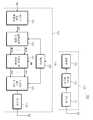
도 1은 본 발명의 제 1 실시 예에 따른 데이터 전송 장치를 보여주는 블록도이다.
도 2는 도 1의 입력 심볼 매핑부 및 푸리에 역 변환부를 보여주는 블록도이다.
도 3은 제 1 내지 제 20 부반송파들의 주파수 스팩트럼들을 개략적으로 보여주는 도면이다.
도 4는 푸리에 역 변환부의 입력 포인트들에 입력되는 신호를 보여주는 테이블이다.
도 5는 입력 심볼 매핑부 및 푸리에 역 변환부의 다른 실시 예를 보여주는 블록도이다.
도 6은 도 5의 푸리에 역 변환부의 입력 포인트들에 입력되는 신호를 보여주는 테이블이다.
도 7은 도 6의 테이블에 따른 신호들이 입력 포인트들에 수신되는 경우, 제 1 내지 제 16 부반송파들의 주파수 스팩트럼을 보여준다.
도 8은 입력 심볼 매핑부 및 푸리에 역 변환부의 또 다른 실시 예를 보여주는 블록도이다.
도 9는 도 8의 푸리에 역 변환부의 입력 포인트들에 입력되는 신호들의 예를 보여주는 테이블이다.
도 10은 도 9의 테이블에 따른 신호가 입력 포인트들에 수신되는 경우, 제 1 내지 제 32 부반송파들의 주파수 스팩트럼들을 보여준다.
도 11은 도 8의 푸리에 역 변환부의 입력 포인트들에 입력되는 신호들의 다른 예를 보여주는 테이블이다.
도 12는 입력 포인트들에 도 11의 테이블에 따른 신호가 수신되는 경우에 제 1 내지 제 32 부반송파들의 주파수 스팩트럼들을 보여준다.
도 13은 본 발명의 다른 실시 예에 따른 입력 심볼 매핑부 및 푸리에 역 변환부를 보여주는 블록도이다.
도 14는 도 1의 제어부에서 발생되는 제어 신호들을 예시적으로 보여주는 테이블이다.
도 15는 본 발명의 제 2 실시 예에 따른 데이터 전송 장치를 보여주는 블록도이다.1 is a block diagram illustrating a data transmission apparatus according to a first embodiment of the present invention.
FIG. 2 is a block diagram illustrating an input symbol mapping unit and a Fourier inverse transform unit of FIG. 1.
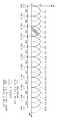
3 is a diagram schematically showing frequency spectra of first to twentieth subcarriers.
4 is a table illustrating a signal input to input points of a Fourier inverse transform unit.
5 is a block diagram illustrating another embodiment of an input symbol mapping unit and a Fourier inverse transform unit.
FIG. 6 is a table illustrating signals input to input points of the Fourier inverse converter of FIG. 5.
FIG. 7 shows the frequency spectrum of the first to sixteenth subcarriers when signals according to the table of FIG. 6 are received at input points.
8 is a block diagram illustrating another embodiment of an input symbol mapping unit and a Fourier inverse transform unit.
FIG. 9 is a table illustrating examples of signals input to input points of the Fourier inverse converter of FIG. 8.
FIG. 10 shows frequency spectra of first to thirty-second subcarriers when a signal according to the table of FIG. 9 is received at input points.
FIG. 11 is a table illustrating another example of signals input to input points of the Fourier inverse converter of FIG. 8.
FIG. 12 shows frequency spectra of the first to 32nd subcarriers when a signal according to the table of FIG. 11 is received at input points.
FIG. 13 is a block diagram illustrating an input symbol mapping unit and a Fourier inverse transform unit, according to another exemplary embodiment.
14 is a table exemplarily illustrating control signals generated by the controller of FIG. 1.
15 is a block diagram illustrating a data transmission apparatus according to a second embodiment of the present invention.
앞의 일반적인 설명 및 다음의 상세한 설명 모두 예시적이라는 것이 이해되어야 하며, 청구된 발명의 부가적인 설명이 제공되는 것으로 여겨져야 한다. 다음의 상세한 설명에서, 참조 부호들이 본 발명의 바람직한 실시 예들에 상세히 표시되어 있으며, 그것의 예들이 참조 도면들에 표시되어 있다.It is to be understood that both the foregoing general description and the following detailed description are exemplary, and that additional explanations of the claimed invention are provided. In the following detailed description, reference numerals are shown in detail in preferred embodiments of the invention, examples of which are shown in the reference figures.
명세서 전체에서, 어떤 부분이 다른 "연결"되어 있다고 할 때, 이는 "직접적으로 연결"되어 있는 경우뿐 아니라, 그 중간에 다른 소자를 사이에 두고 "간접적으로 연결"되어 있는 경우도 포함한다. 명세서 전체에서, 어떤 부분이 어떤 구성요소를 "포함"한다고 할 때, 이는 특별히 반대되는 기재가 없는 한 다른 구성요소를 제외하는 것이 아니라 다른 구성요소를 더 포함할 수 있는 것을 의미한다.Throughout the specification, when a part is said to be "connected" differently, this includes not only the case where it is "directly connected" but also the case where it is "indirectly connected" with another element in between. Throughout the specification, when a part is said to "include" a certain component, it means that it can further include other components, without excluding other components unless specifically stated otherwise.
도 1은 본 발명의 제 1 실시 예에 따른 데이터 전송 장치(100)를 보여주는 블록도이다. 도 1을 참조하면, 데이터 전송 장치(100)는 검출 블록(110) 및 데이터 전송 블록(120)을 포함한다.1 is a block diagram illustrating a
검출 블록(110)은 외부에서 점유되는(또는, 사용되는) 무선 주파수 신호가 포함되는 서브 주파수 대역을 검출한다. 그리고, 검출 블록(110)은 검출된 서브 주파수 대역에 대한 정보(FBI)를 제어부(125)에 전송한다.The
검출 블록(110)은 수신부(111), 에너지 계산부(112) 및 검출부(113)를 포함한다. 수신부(111)는 외부로부터 무선 주파수(Radio Frequency,RF) 신호를 수신한다. 수신부(111)는 수신되는 무선 주파수 신호들 중 미리 정해진 주파수 대역(예를 들면, MICS 대역 전체)을 선택한다. 선택된 대역의 무선 주파수 신호는 에너지 계산부(112)에 전송된다.The
예시적으로, 수신부(111)는 로우 패스 필터(Low Pass Filter)들, 하이 패스 필터(High Pass Filter)들 및 밴드 패스 필터(Band Pass Filter)들 중 어느 하나, 또는 그것들 중 적어도 2개의 조합을 포함할 수 있다.In exemplary embodiments, the
에너지 계산부(112)는 수신부(111)로부터 무선 주파수 신호를 수신한다. 에너지 계산부(112)는 복수의 서브 주파수 대역들 각각의 에너지 값을 계산한다. 하나의 서브 주파수 대역은 하나의 부반송파(예를 들면, SC1~SC20 중 어느 하나)가 위치하는 주파수 영역을 의미한다.The
예시적으로, 무선 주파수 신호가 포함된 서브 주파수 대역의 에너지 값은 무선 주파수 신호가 포함되지 않은 서브 주파수 대역의 에너지 값보다 클 것이다. 예시적으로, 에너지 계산부(112)는 각 서브 주파수 대역 내의 무선 주파수 신호의 진폭(Amplitude)의 절대값(또는, 절대값의 제곱)을 계산함으로써, 각 서브 주파수 대역의 에너지 값을 계산할 수 있다. In exemplary embodiments, an energy value of a sub frequency band in which the radio frequency signal is included may be greater than an energy value of a sub frequency band in which the radio frequency signal is not included. For example, the
검출부(113)는 에너지 계산부(112)에서 계산된 에너지 값을 이용하여 외부에서 사용되는 서브 주파수 대역을 검출한다. 예시적으로, 검출부(113)는 각 서브 주파수 대역의 에너지 값 중 임계값보다 큰 에너지 값을 가지는 서브 주파수 대역을 검출할 것이다. 검출된 서브 주파수 대역에 대한 정보(FBI, 이하 서브 주파수 대역 정보)는 제어부(125)에 전송된다.The
데이터 전송 블록(120)은 직교 주파수 분할(Orthogonal Frequency Division Meltiplexing, 이하 "OFDM"이라고 한다) 방식에 따라 데이터 심볼들을 부반송파들로 변환하고, 변환된 부반송파들을 외부로 전송한다.The
데이터 전송 블록(120)은 데이터 심볼 매핑부(121), 입력 심볼 매핑부(122), 푸리에 역 변환부(123), 사이드 로브(side lobe) 제거부(124), 제어부(125), 및 전송부(126)를 포함한다.The
데이터 심볼 매핑부(121)는 직렬 비트 스트림들(BS)을 수신한다. 예를 들면, 직렬 비트 스트림들(BS)은 영상 데이터, 음성 데이터 또는 텍스트 데이터 등일 수 있다. 데이터 심볼 매핑부(121)는 직렬 비트 스트림들(BS)을 복수의 그룹들로 구분하고, 복수의 그룹들 각각을 복수의 데이터 심볼들에 매핑한다. 매핑된 복수의 데이터 심볼들은 직렬의 데이터 심볼들(SDS)을 구성한다. 직렬의 데이터 심볼들(SDS)은 입력 심볼 매핑부(122)에 전송된다.The data
예시적으로, 데이터 심볼 매핑부(121)는 직교 위상 편이 변조(Quadrature Phase Shift Keying,QPSK) 및 직교 진폭 변조(Quadrature Amplitude Modulation,QAM) 중 적어도 하나를 수행함으로써 직렬의 데이터 심볼들(SDS)을 생성할 수 있다. 예를 들면, 데이터 심볼 매핑부(121)는 직렬의 비트 스트림들(BS)을 구성하는 디지털 데이터를 4개의 위상에 대응시킴으로써 데이터 심볼들(SDS)을 생성할 것이다. 예를 들면, 데이터 심볼 매핑부(121)는 진폭 편이(Amplitude Shift Keying,ASK) 및 위상 편이(Phase Shift Keying,PSK) 모두를 이용한 변조 방식에 따라 직렬의 데이터 심볼들(SDS)을 생성할 것이다.In an exemplary embodiment, the data
입력 심볼 매핑부(122)는 제어부(125)의 제어에 따라 동작한다. 입력 심볼 매핑부(122)는 직렬의 데이터 심볼들(SDS)을 수신하고, 매핑된 심볼들(MDS1~MDSk)을 생성한다. 매핑된 심볼들(MDS1~MDSk)은 푸리에 역 변환부(123)의 입력 포인트들(도 2의 a 참조)에 전송된다.The input
입력 심볼 매핑부(122)는 직렬의 데이터 심볼들(SDS)을 병렬의 데이터 심볼들로 변환할 것이다. 그리고, 입력 심볼 매핑부(122)는 병렬의 데이터 심볼들을 이용하여 매핑된 심볼들(MDS1~MDSk)을 발생한다.The input
입력 심볼 매핑부(122)는 서브 주파수 대역 정보(FBI)에 대응하는 입력 포인트에 널 신호를 매핑한다. 입력 심볼 매핑부(122)는 부반송파들(SC1~SCk)의 주 로브(main lobe)가 중첩되지 않도록 푸리에 역 변환부(123)의 입력 포인트들 중 일부에 널(null) 신호들을 매핑한다. 그리고, 입력 심볼 매핑부(122)는 나머지의 입력 포인트들에 병렬의 데이터 심볼들을 매핑한다. 예를 들면, 각각의 널 신호와 각각의 병렬의 데이터 심볼은 교대로 매핑될 것이다.The input
푸리에 역 변환부(123)는 제어부(125)의 제어에 따라 푸리에 역 변환을 수행한다. 푸리에 역 변환부(123)는 제어부(125)로부터 대역폭 정보(BW)를 수신한다. 푸리에 역 변환은 대역폭 정보(BW)에 대응하는 대역폭 내에서 수행될 것이다. 푸리에 역 변환부(123)는 OFDM 방식에 따라 매핑된 심볼들(MDS1~MDSk)을 각각 부반송파들(SC1~SCk)로 변환할 것이다. 매핑된 심볼들(MDS1~MDSk)은 서로 중첩되는 서브 주파수 대역들을 이용하여 변환될 것이다. 부반송파들(SC1~SCk)은 서로 직교성(orthogonal)을 갖을 것이다. 예시적으로, 푸리에 역 변환부(123)로부터 출력된 복수의 부반송파들(SC1~SCk)은 기저 대역(baseband) 내의 신호들일 것이다.The Fourier
생성된 부반송파들(SC1~SCk)은 하나의 OFDM 심볼을 구성할 것이다. 예시적으로, 푸리에 역 변환부(123)는 Inverse Fast Fourier Transform(IFFT) 알고리즘에 따라 푸리에 역 변환을 수행할 수 있다.The generated subcarriers SC1 to SCk may constitute one OFDM symbol. For example, the Fourier
사이드 로브 제거부(124)는 제어부(125)의 제어에 따라 동작한다. 사이드 로브 제거부(124)는 병렬의 부반송파들(SC1~SCk)을 직렬의 부반송파들로 변환한다. 직렬의 부반송파들은 하나의 OFDM 심볼을 구성할 것이다. 그리고, 사이드 로브 제거부(124)는 OFDM 심볼에 포함된 부반송파들의 사이드 로브(side lobe)를 제거한다. 예를 들면, 사이드 로브는 각 부반송파의 주로브를 제외한 진폭을 의미할 것이다. 예를 들면, 사이드 로브는 각 부반송파가 포함되는 서브 주파수 대역을 벗어나는 부반송파의 진폭을 의미할 것이다.The side
예시적으로, 사이드 로브 제거부(124)는 보호 구간(Guard Interval,GI) 부가 및 윈도윙(windowing)을 수행하여 사이드 로브를 제거할 수 있다. 예를 들면, 사이드 로브 제거부(124)는 연속된 직렬의 OFDM 심볼들 각각에 보호 구간으로서 프리픽스(prefix)와 서픽스(suffix)를 부가한다. 그리고, 사이드 로브 제거부(124)는 프리픽스와 서픽스가 부가된 OFDM 심볼들에 윈도윙 함수를 곱함으로써 OFDM 심볼들 각각의 진폭의 절대값을 감소시킬 것이다. OFDM 심볼들 각각의 진폭의 절대값이 감소됨에 따라, OFDM 심볼들 각각에 포함된 부반송파들의 절대값들도 감소할 것이다. 결과적으로, OFDM 심볼들 각각에 포함된 부반송파들의 사이드 로브는 제거될 것이다.For example, the side
전송부(126)는 사이드 로브가 제거된 직렬의 OFDM 심볼들을 고주파수 대역(예를 들면, MICS 대역의 주파수)의 신호들로 변환하고, 변환된 신호들을 외부로 전송한다(b). 예를 들면, 전송부(126)는 직렬의 OFDM 심볼의 주파수를 401.1MHz만큼 증가시킨다.The
도 2는 도 1의 입력 심볼 매핑부(122) 및 푸리에 역 변환부(123)를 보여주는 블록도이다. 도 2의 실시 예에 있어서, 푸리에 역 변환부(123)는 20개의 입력 포인트들(a) 및 출력 포인트들(b)을 가진다. 도 2의 실시 예에 있어서, 병렬 변환기(210)는 9개의 병렬의 데이터 심볼들(PDS1~PDS9)을 발생한다.FIG. 2 is a block diagram illustrating an input
도 1 및 도 2를 참조하면, 입력 심볼 매핑부(122)는 병렬 변환기(210) 및 할당기(220)를 포함한다. 병렬 변환기(210)는 직렬의 데이터 심볼들(SDS)을 수신한다. 병렬 변환기(210)는 제어부(125)로부터 병렬 데이터 심볼들의 개수 정보(PDSI)를 수신한다.1 and 2, the input
병렬 데이터 심볼들의 개수 정보(PDSI)가 가리키는 최대 값은, 대역폭 정보(BW)가 가리키는 대역폭에 포함되는 주파수 채널들(예를 들면, MISC 대역의 주파수 채널들 중 대역폭에 포함되는 주파수 채널들) 중 외부에서 사용되는 주파수 채널을 제외한 것의 개수일 것이다. 예를 들면, 푸리에 역 변환부(123)가 0.9~3.3MHz(MICS 대역에서는 402~404.4MHz)에 대응하는 대역폭 정보(BW)를 수신하고, 수신된 대역폭 정보(BW)에 따라 푸리에 역 변환을 수행한다고 가정한다. MICS 대역 중 8 개의 주파수 채널들(CH1~CH8)이 402~404.4MHz에 포함될 것이다. 외부에서 사용되는 서브 주파수 대역이 제 3 주파수 채널(CH3)에 포함되는 경우에(즉, 한 개의 채널만 검출된 경우), 병렬 데이터 심볼들의 개수 정보(PDSI)의 최대 값은 7이다.The maximum value indicated by the number information PDSI of the parallel data symbols is one of frequency channels included in the bandwidth indicated by the bandwidth information BW (for example, frequency channels included in the bandwidth among the frequency channels of the MISC band). It will be the number except the frequency channel used externally. For example, the Fourier
제어부(125)는 수신된 서브 주파수 대역 정보(FBI)에 따라 병렬 데이터 심볼들의 개수 정보(PDSI)를 생성할 것이다. 예시적으로, 제어부(125)는 MICS 대역의 주파수 채널들 중 서브 주파수 대역 정보(FBI)에 대응하는 주파수 채널을 제외한 주파수 채널들의 개수에 따라 병렬 데이터 심볼들의 개수 정보(PDSI)를 생성할 것이다.The
병렬 변환기(210)는 병렬 데이터 심볼들의 개수 정보(PDSI)에 따라 직렬의 데이터 심볼들(SDS)을 병렬의 데이터 심볼들(PDS1~PDS9)로 변환한다. 이때, 병렬 변환기(210)는 연속적으로 수신되는 직렬의 데이터 심볼들(SDS)을 복수의 그룹들로 구분하고, 각 그룹을 병렬의 데이터 심볼들(PDS1~PDS9)로 변환할 것이다.The
할당기(220)는 제 1 내지 제 9 병렬의 데이터 심볼들(PDS1~PDS9)을 수신한다. 할당기(220)는 제어부(125)로부터 널 포인트 정보(NP)를 수신한다.The
할당기(220)는 입력 포인트들(a) 중 널 포인트 정보(NP)에 대응하는 입력 포인트에 널(null) 신호를 전송한다. 또한, 할당기(220)는 널 포인트 정보(NP)에 대응하는 입력 포인트를 제외한 입력 포인트들 중 일부에 널 신호를 제공한다. 그리고, 할당기(220)는 널 포인트 정보(NP)에 대응하는 입력 포인트를 제외한 입력 포인트들 중 다른 일부에 병렬의 데이터 심볼들(PDS1~PDS9)을 제공한다. 예를 들면, 할당기(220)는 각 입력 포인트에 널 신호와 병렬의 데이터 심볼을 교대로 제공한다.The
널 포인트 정보(NP)는 서브 주파수 대역 정보(FBI)에 기반하여 제공될 것이다. 널 포인트 정보(NP)는 입력 포인트에 대한 정보이다. 예시적으로, 대역폭 정보(BW)의 대역폭 값과 입력 포인트들의 개수를 이용하면, 입력 포인트들(a)에 각각 대응하는 서브 주파수 대역들이 계산된다. 제어부(125)는 입력 포인트들(a)에 각각 대응하는 서브 주파수 대역들을 참조하여 서브 주파수 대역 정보(FBI)에 대응하는 입력 포인트를 판별할 것이다. 제어부(125)는 검출된 입력 포인트에 대한 정보인 널 포인트 정보(NP)를 할당기(220)에 전송할 것이다.The null point information NP will be provided based on the sub frequency band information FBI. The null point information NP is information on an input point. For example, when the bandwidth value of the bandwidth information BW and the number of input points are used, sub-frequency bands corresponding to the input points a are respectively calculated. The
또한, 할당기(220)는 제 1 내지 제 20 부반송파들(SC1~SC20)이 서로 중첩되지 않도록 입력 포인트들(a) 중 일부에 각각 널 신호들을 전송할 것이다. 그리고, 할당기(220)는 나머지 입력 포인트들에 각각 제 1 내지 제 9 병렬의 데이터 심볼들(PDS1~PDS9)을 전송할 것이다. 할당기(220)로부터 전송되는 널 신호들, 및 제 1 내지 제 9 병렬의 데이터 심볼들(PDS1~PDS9)은 제 1 내지 제 20 매핑된 심볼들(MDS1~MDS20)을 구성할 것이다.In addition, the
푸리에 역 변환부(123)는 제 1 내지 제 20 입력 포인트들(a)을 통해 각각 제 1 내지 제 20 매핑된 심볼들(MDS1~MDS20)을 수신한다. 푸리에 역 변환부(123)는 제 1 내지 제 20 매핑된 심볼들(MDS1~MDS20)을 각각 푸리에 역 변환하여 제 1 내지 제 20 부반송파들(SC1~SC20)을 발생한다.The Fourier
제 1 내지 제 20 입력 포인트들(a)은 각각 복수의 서브 주파수 대역들에 대응할 것이다. 푸리에 역 변환부(123)는 각 매핑된 심볼을 각 입력 포인트에 대응하는 서브 주파수 대역을 기준으로 푸리에 역 변환할 것이다. 그리고, 푸리에 역 변환부(123)는 제 1 내지 제 20 출력 포인트들(b)을 통해 각각 제 1 내지 제 20 부반송파들(SC1~SC20)을 발생할 것이다.The first through twentieth input points a may each correspond to a plurality of sub frequency bands. The Fourier
MICS 프로토콜이 적용될 통신 기기들은, 데이터 전송에 사용되는 부반송파들 상호간의 간격(예를 들면, 데이터 전송에 사용되는 부반송파들의 중심 주파수들 각각의 간격)이 300KHz를 유지하고, 부반송파들은 서로 중첩되지 않아야 한다. 그리고, MICS 대역의 각 주파수 채널에 대응하는 부반송파들의 신호 중 주파수 채널을 벗어나는 신호는 피크 값과 비교해서 -20dB 이하로 유지되어야 한다.For communication devices to which the MICS protocol is to be applied, the spacing between subcarriers used for data transmission (for example, the spacing of each of the center frequencies of subcarriers used for data transmission) should be 300 KHz, and the subcarriers should not overlap each other. . In addition, the signal leaving the frequency channel among the signals of the subcarriers corresponding to each frequency channel of the MICS band should be kept below -20 dB compared to the peak value.
한편, 푸리에 역 변환부(123)에서 발생된 부반송파들(SC1~SC20)은 직교성을 갖는다. 따라서, 매핑된 심볼들(MDS1~MDS20)에 널 신호가 포함되지 않는 경우에, 부반송파들(SC1~SC20)의 주 로브들은 서로 겹칠 것이다.Meanwhile, the subcarriers SC1 to SC20 generated by the Fourier
본 발명의 실시 예에 따르면, 할당기(220)는 부반송파들(SC1~SC20)의 주 로브들이 서로 겹치지 않도록 입력 포인트들 중 일부에 널 신호를 전송한다. 예시적으로, 할당기(220)는 제 1 내지 제 9 병렬의 데이터 심볼들(PDS1~PDS9), 그리고 널 신호들을 교대로 입력 포인트들(a)에 전송한다.According to an embodiment of the present invention, the
널 신호들이 푸리에 역 변환 됨에 따른 부반송파(이하, 널 부반송파)의 진폭(amplitude)은 매우 작을 것이다. 따라서, 부반송파들(SC1~SC20)의 직교성에 따라 부반송파들(SC1~SC20)의 주 로브가 겹치는 현상은 발생되지 않을 것이다.As the null signals are inversely Fourier transformed, the amplitude of a subcarrier (hereinafter, referred to as a null subcarrier) will be very small. Accordingly, the phenomenon that the main lobes of the subcarriers SC1 to SC20 overlap with each other according to the orthogonality of the subcarriers SC1 to SC20 will not occur.
본 발명의 실시 예에 따르면, 할당기(220)는 입력 포인트들(a) 중 서브 주파수 대역 정보(FBI)에 대응하는 입력 포인트에 병렬의 데이터 심볼들(PDS1~PDS9)을 할당하지 않는다. 제어부(125)는, 할당기(220)가 서브 주파수 대역 정보(FBI)에 대응하는 입력 포인트에 널 신호를 전송하도록 할당기(220)를 제어할 것이다. 따라서, 데이터 전송 장치(100)는 MICS 대역의 채널들 중 서브 주파수 대역 정보(FBI)에 대응하는 주파수 채널을 데이터 전송에 사용하지 않을 것이다. 결과적으로, 데이터 전송 장치(100)는 외부에서 사용되는 서브 주파수 대역을 포함하는 주파수 채널을 데이터 전송에 사용하지 않을 것이다.According to an embodiment of the present disclosure, the
도 3은 제 1 내지 제 20 부반송파들(SC1~SC20)의 주파수 스팩트럼들을 개략적으로 보여주는 도면이다. MICS 대역에 해당하는 주파수 값들은 괄호 안에 표시된다.3 is a diagram schematically showing frequency spectra of the first to twentieth subcarriers SC1 to SC20. Frequency values corresponding to the MICS band are shown in parentheses.
도 1 내지 도 3을 참조하면, 푸리에 역 변환부(123)는 0.9~3.9 MHz 내의 제 1 내지 제 20 부반송파들(SC1~SC20)을 발생할 것이다. 그리고, 전송부(126)는 0.9~3.9 MHz 내의 제 1 내지 제 20 부반송파들(SC1~SC20)을 402~405 MHz 내의 제 1 내지 제 20 부반송파들(SC1~SC20)로 변환할 것이다.1 to 3, the Fourier
MISC 대역(402~405MHz)은 제 1 내지 제 10 주파수 채널들(CH1~CH10)로 구성된다. 제 1 내지 제 10 주파수 채널들(CH1~CH10)은 각각 적어도 하나의 서브 주파수 대역을 포함한다. 점선으로 도시된 부반송파들은 널 부반송파이다. 그리고, 제 5 부반송파(SC5)는 널 부반송파이다.The
도 3을 참조한 설명에서, 제 3 주파수 채널(CH3)이 서브 주파수 대역 정보(FBI)에 대응하는 것으로 가정한다. 입력 포인트들(a) 중 서브 주파수 대역 정보(FBI)에 대응하는 입력 포인트(도 2에서는 제 5 입력 포인트)에 널 신호가 전송됨으로써, 널 부반송파인 제 5 부반송파(SC5)가 발생된다. 즉, 외부에서 사용되는 서브 주파수 대역이 제 3 주파수 채널(CH3)에 해당되는 경우에, 데이터 전송 장치(100)는 제 3 주파수 채널(CH3)을 통해 무선 주파수를 전송하지 않는다.In the description with reference to FIG. 3, it is assumed that the third frequency channel CH3 corresponds to the sub frequency band information FBI. A null signal is transmitted to an input point (a fifth input point in FIG. 2) corresponding to the sub frequency band information FBI among the input points a, thereby generating a fifth subcarrier SC5 that is a null subcarrier. That is, when the sub frequency band used externally corresponds to the third frequency channel CH3, the
입력 포인트들(a) 중 일부에 널 신호가 전송됨으로써, 점선으로 도시된 널 부반송파들이 발생된다. 예를 들면, 입력 포인트들(a) 중 짝수 입력 포인트들에 널 신호가 전송됨으로써, 점선으로 도시된 널 부반송파들이 발생된다. 부반송파들(SC1~SC20)의 주 로브들은 서로 중첩되지 않을 것이다. 예시적으로, 부반송파들의 주 로브가 -20dB 이상에서 형성된다고 가정하면, 널 부반송파들은 -20dB 이상에서 주파수 스팩트럼을 갖지 않는다.By sending a null signal to some of the input points a, null subcarriers shown in dashed lines are generated. For example, a null signal is transmitted to even input points among the input points a, thereby generating null subcarriers shown by dotted lines. The primary lobes of the subcarriers SC1-SC20 will not overlap each other. By way of example, assuming that the primary lobes of subcarriers are formed above -20 dB, null subcarriers do not have a frequency spectrum above -20 dB.
결과적으로, 제 1 내지 제 9 병렬의 데이터 심볼들(PDS1~PDS9)은 각각 제 1 및 제 2 주파수 채널들(CH1,CH2), 그리고 제 4 내지 제 10 주파수 채널들(CH4,CH10)을 통해 전송될 것이다.As a result, the data symbols PDS1 to PDS9 in the first to ninth parallels are respectively transmitted through the first and second frequency channels CH1 and CH2 and the fourth to tenth frequency channels CH4 and CH10. Will be sent.
도 3의 실시 예에 따른 데이터 전송 장치(100)는 제 1 내지 제 10 주파수 채널들(CH1~CH10) 내에 병렬의 데이터 심볼들(PDS1~PDS9)에 대응하는 부반송파들, 및 널 부반송파들을 교대로 배치한다. 추가적으로, 데이터 전송 장치(100)는 외부에서 사용되는 서브 주파수 대역에 널 부반송파를 배치한다.The
본 발명의 실시 예에 따르면, 복수의 주파수 채널들을 통해 부반송파들을 전송함으로써 향상된 데이터 전송률을 가지는 데이터 전송 장치(100)가 제공된다. 또한, 본 발명의 실시 예에 따르면, MICS 대역의 하나의 주파수 채널을 통해 하나의 부반송파가 전송된다.According to an embodiment of the present invention, a
도 4는 푸리에 역 변환부(123)의 입력 포인트들(a)에 입력되는 신호를 보여주는 테이블이다. 도 2 내지 도 4를 참조하면, 입력 포인트들(a) 중 짝수 입력 포인트들에 널 신호가 입력된다. 도 4에서 널 신호의 논리 상태는 '0'인 것으로 도시된다. 또한, 제 5 입력 포인트에 널 신호가 입력된다. 제 1 내지 제 9 병렬의 데이터 심볼들(PDS1~PDS9)은 각각 나머지 입력 포인트들에 입력된다. 도 4의 테이블에 따라 매핑된 심볼들(MDS1~MDS20)이 전송되면, 부반송파들(SC1~SC20)의 주파수 스팩트럼은 도 3과 같이 나타난다.4 is a table illustrating a signal input to the input points a of the Fourier
도 5는 입력 심볼 매핑부(122) 및 푸리에 역 변환부(123)의 다른 실시 예를 보여주는 블록도이다. 도 5를 참조하면, 병렬 변환기(210)는 병렬 데이터 심볼들의 개수 정보(PDSI)에 따라 직렬의 데이터 심볼들(SDS)을 병렬의 데이터 심볼들(PDS1~PDS7)로 변환한다.5 is a block diagram illustrating another embodiment of the input
도 5의 실시 예에서, 할당기(122)는 16개의 매핑된 심볼들(MDS1~MDS16)을 발생할 것이다. 할당기(122)는 널 포인트 정보(NP)에 대응하는 입력 포인트에 널 신호를 전송할 것이다. 예시적으로, 널 포인트 정보(NP)는 적어도 하나의 입력 포인트에 대응될 것이다. 할당기(122)는 입력 포인트들(c) 중 일부에 널 신호를 전송할 것이다. 그리고, 할당기(122)는 입력 포인트들(c) 중 나머지 일부에 제 1 내지 제 7 병렬의 데이터 심볼들(PDS1~PDS7)을 전송할 것이다.In the embodiment of FIG. 5,
도 6은 도 5의 푸리에 역 변환부(123)의 입력 포인트들(c)에 입력되는 신호를 보여주는 테이블이다. 도 5 및 도 6을 참조하면, 입력 포인트들(c) 중 짝수 입력 포인트들에 널 신호가 입력된다. 추가적으로, 할당기(122)는 널 포인트 정보(NP)에 대응하는 입력 포인트(도 6에서는 제 5 입력 포인트)에 널 신호를 전송할 것이다. 그리고, 할당기(122)는 나머지 입력 포인트들에 제 1 내지 제 7 병렬의 데이터 심볼들(PDS1~PDS7)을 전송할 것이다.FIG. 6 is a table illustrating signals input to input points c of the Fourier
도 7은 도 6의 테이블에 따른 신호들이 입력 포인트들(c)에 수신되는 경우, 제 1 내지 제 16 부반송파들(SC1~SC16)의 주파수 스팩트럼을 보여준다. 푸리에 역 변환부(123)는 0.9~3.3MHz 내에 위치하는 제 1 내지 제 16 부반송파들(SC1~SC16)을 발생할 것이다. 0.9~3.3MHz의 주파수 대역은 대역폭 정보(BW)에 의해 정해질 것이다. 2.4MHz의 대역폭 내에서, 16개의 입력 포인트들을 가지는 푸리에 역 변환부(123)의 출력 반송파들은 각각 300kHz의 대역폭을 갖을 것이다.FIG. 7 illustrates frequency spectrums of the first to sixteenth subcarriers SC1 to SC16 when signals according to the table of FIG. 6 are received at the input points c. The Fourier
도 7을 참조하면, 7개의 병렬의 데이터 심볼들(PDS1~PDS7)이 입력 포인트들 중 일부에 입력됨에 따라, -20dB이상의 주 로브를 가지는 부반송파들이 7개 형성된다. 다른 말로, 데이터 전송 장치(100)는 제 3 주파수 채널(CH3)을 제외한 7개의 주파수 채널들(CH1,CH2,CH4~CH8)을 통해 데이터를 전송할 것이다. Referring to FIG. 7, as seven parallel data symbols PDS1 to PDS7 are input to some of the input points, seven subcarriers having a main lobe of −20 dB or more are formed. In other words, the
도 7은 예시적인 도면으로서, 데이터 전송 장치(100)는 제 4 내지 제 10 주파수 채널들(CH4~CH10)을 통해 데이터를 전송할 수 있음이 이해될 것이다.FIG. 7 is an exemplary diagram, and it will be understood that the
도 8은 입력 심볼 매핑부(122) 및 푸리에 역 변환부(123)의 또 다른 실시 예를 보여주는 블록도이다. 도 8의 병렬 변환기(210)는 병렬 데이터 심볼들의 개수 정보(PDSI)에 따라 7개의 병렬의 데이터 심볼들(PDS1~PDS7)을 발생한다.8 is a block diagram illustrating still another embodiment of the input
도 9는 도 8의 푸리에 역 변환부(123)의 입력 포인트들(e)에 입력되는 신호들의 예를 보여주는 테이블이다. 도 8 및 도 9을 참조하면, 할당기(220)는 푸리에 역 변환부(123)에서 출력되는 부반송파들(SC1~SC32)의 주 로브들이 중첩되지 않도록 입력 포인트들 중 일부에 널 신호를 전송할 것이다. 할당기(220)는 널 포인트 정보(NP)에 대응하는 입력 포인트(도 8에서 제 10 입력 포인트)에 널 신호를 전송할 것이다. 그리고, 할당기(220)는 나머지 입력 포인트들에 제 1 내지 제 7 병렬의 데이터 심볼들(PDS1~PDS7)을 전송할 것이다. 도 9에서는 제 1 내지 제 7 병렬의 데이터 심볼들(PDS1~PDS7)이 각각 제 2,6,14,18,22,26, 및 30 입력 포인트들에 입력된다.FIG. 9 is a table illustrating examples of signals input to input points e of the Fourier
도 10은 도 9의 테이블에 따른 신호가 입력 포인트들(e)에 수신되는 경우, 제 1 내지 제 32 부반송파들(SC1~SC32)의 주파수 스팩트럼들을 보여준다. 도 10에서, 주파수가 증가함에 따라 순차적으로 배치되는 주 로브들은 각각 제 1 내지 제 32 부반송파들(SC1~SC32,도 7 참조)의 주 로브들임이 이해될 것이다.FIG. 10 shows frequency spectra of the first to 32nd subcarriers SC1 to SC32 when a signal according to the table of FIG. 9 is received at the input points e. In FIG. 10, it will be understood that the main lobes sequentially arranged as the frequency increases are the main lobes of the first to 32nd subcarriers SC1 to SC32 (see FIG. 7), respectively.
도 8 내지 도 10을 참조하면, 푸리에 역 변환부(123)는 입력 포인트들(e)을 통해 수신되는 신호들을 역 변환하여 제 1 내지 제 32 부반송파들(SC1~SC32)을 발생할 것이다. 푸리에 역 변환부(123)는 0.9~3.3MHz(MICS 대역에서는 402~404.4MHz) 내에 위치하는 제 1 내지 제 32 부반송파들(SC1~SC32)을 발생할 것이다. 0.9~3.3MHz의 주파수 대역은 대역폭 정보(BW)에 의해 정해질 것이다. 2.4MHz의 대역폭 내에서, 제 1 내지 제 32 부반송파들은 각각 150kHz의 대역폭을 갖는다.8 to 10, the Fourier
서브 주파수 대역 정보(FBI)에 대응하는 제 10 입력 포인트에 널 신호가 입력됨에 따라, 제 3 주파수 채널(CH3)에 널 부반송파가 위치한다. 그리고, 제 2,6,14,18,22,26, 및 30 입력 포인트들을 제외한 나머지 입력 포인트들에 널 신호가 입력됨에 따라, 점선으로 도시된 널 부반송파들이 위치한다. 결과적으로, 부반송파들의 주 로브는 서로 중첩되지 않는다.As the null signal is input to the tenth input point corresponding to the sub frequency band information FBI, the null subcarrier is positioned in the third frequency channel CH3. As null signals are input to the remaining input points except for the second, six, fourteen, eighteen, twenty-two, and thirty input points, null subcarriers shown by dotted lines are positioned. As a result, the main lobes of subcarriers do not overlap each other.
도 11은 도 8의 푸리에 역 변환부(123)의 입력 포인트들(e)에 입력되는 신호들의 다른 예를 보여주는 테이블이다. 도 11 및 도 12를 참조한 설명에서, 서브 주파수 대역 정보(FBI)는 제 11 입력 포인트에 대응하는 것으로 가정한다. 제 11 입력 포인트에 널 신호가 전송될 것이다. 제 11 입력 포인트를 제외한 입력 포인트들 중 일부에 널 신호들이 전송될 것이다. 제 11 입력 포인트를 제외한 입력 포인트들 중 나머지 일부에 9개의 병렬의 데이터 심볼들(PDS1~PDS9)이 전송될 것이다.FIG. 11 is a table illustrating another example of signals input to input points e of the Fourier
도 12는 입력 포인트들(e)에 도 11의 테이블에 따른 신호가 수신되는 경우에 제 1 내지 제 32 부반송파들의 주파수 스팩트럼들을 보여준다. 도 12의 실시 예에 따르면, 푸리에 역 변환부(123)는 0~4.8 MHz 내에 위치하는 제 1 내지 제 32 부반송파들(SC1~SC32)을 발생할 것이다. 0~4.8 MHz의 주파수 대역은 대역폭 정보(BW)에 따라 정해질 것이다. 4.8MHz의 대역폭 내에서, 32개의 입력 포인트들을 가지는 푸리에 역 변환부(123)의 출력 반송파들은 각각 300kHz의 대역폭을 갖는다.FIG. 12 shows frequency spectra of the first to thirty-second subcarriers when a signal according to the table of FIG. 11 is received at the input points e. According to the embodiment of FIG. 12, the Fourier
도 11 및 도 12를 참조하면, 제 1 내지 제 10 주파수 채널을 벗어나는 서브 주파수 대역들에 대응하는 입력 포인트들(도 11의 테이블에서 제 1 내지 제 6 입력 포인트들, 그리고 제 27 내지 제 32 입력 포인트들)에, 널 신호가 입력된다. 서브 주파수 대역 정보(FBI)에 대응하는 제 11 입력 포인트에 널 신호가 입력된다. 부반송파들의 주 로브들이 서로 중첩되지 않도록, 입력 포인트들(제 7 내지 제 20 입력 포인트들) 중 일부에 널 신호가 입력된다. 그리고, 나머지 입력 포인트들에 제 1 내지 제 9 병렬의 데이터 심볼들(PDS1~PDS9)이 전송된다. 이에 따라, 도 12에 도시된 주파수 대역에 널 부반송파들 및 제 1 내지 제 9 병렬의 데이터 심볼들(PDS1~PDS9)이 위치한다.11 and 12, input points corresponding to sub-frequency bands outside the first to tenth frequency channels (first to sixth input points in the table of FIG. 11, and twenty-seventh to thirty-second inputs) Points), a null signal is input. A null signal is input to the eleventh input point corresponding to the sub frequency band information FBI. A null signal is input to some of the input points (seventh through twentieth input points) so that the primary lobes of the subcarriers do not overlap each other. The first to ninth parallel data symbols PDS1 to PDS9 are transmitted to the remaining input points. Accordingly, null subcarriers and first to ninth parallel data symbols PDS1 to PDS9 are located in the frequency band shown in FIG. 12.
도 13은 본 발명의 다른 실시 예에 따른 입력 심볼 매핑부(310) 및 푸리에 역 변환부(320)를 보여주는 블록도이다. 도 13을 참조하면, 입력 심볼 매핑부(310)는 병렬 변환기(311) 및 할당기(312)를 포함한다. 병렬 변환기(311)는 제어부(125)로부터 수신된 병렬 데이터 심볼들의 개수 정보(PDSI)에 따라 직렬의 데이터 심볼들(SDS)을 제 1 내지 제 7 병렬의 데이터 심볼들(PDS1~PDS7)로 변환한다.FIG. 13 is a block diagram illustrating an input
할당기(312)는 제어부(125)로부터 할당 제어 신호(AC)를 수신한다. 할당 제어 신호(AC)에 따라, 할당기(312)는 매핑된 심볼들(MDS1~MDS32)을 발생한다.The
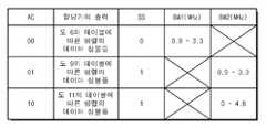
예시적으로, 도 14를 참조하면, 할당 제어 신호(AC)의 논리 상태가 "00"인 경우에, 할당기(312)는 도 6의 테이블에 따른 매핑된 심볼들(MDS1~MDS16)을 발생할 것이다. 이때, 제 17 내지 제 32 매핑된 심볼들(MDS17~MDS32)은 널 신호이다. 할당 제어 신호(AC)의 논리 상태가 "01"인 경우에, 할당기(312)는 도 9의 테이블에 따른 매핑된 심볼들(MDS1~MDS32)을 발생한다. 그리고, 할당 제어 신호(AC)의 논리 상태가 "10"인 경우에, 할당기(312)는 도 11의 테이블에 따른 매핑된 심볼들(MDS1~MDS32)을 발생한다.For example, referring to FIG. 14, when the logic state of the allocation control signal AC is “00,” the
또한, 할당기(312)는 널 포인트 정보(NP)에 대응하는 입력 포인트에 널 신호를 제공할 것이다.The
다시 도 13을 참조하면, 푸리에 역 변환부(320)는 선택기(321), 제 1 및 제 2 푸리에 역 변환 회로들(322,323), 그리고 멀티플렉서(324)를 포함한다. 선택기(321)는 제 1 내지 제 32 매핑된 심볼들(MDS1~MDS32)을 수신한다. 선택기(321)는 제어부(125)로부터 선택 신호(SS)를 수신한다.Referring back to FIG. 13, the Fourier
선택 신호(SS)에 응답하여, 선택기(321)는 제 1 푸리에 역 변환 회로(322)에 제 1 내지 제 16 매핑된 심볼들(MDS1~MDS16)을 전송하거나, 제 2 푸리에 역 변환 회로(323)에 제 1 내지 제 32 매핑된 심볼들(MDS1~MDS32)을 전송한다. 예시적으로, 선택 신호(SS)의 논리 상태가 "0"인 경우에, 선택기(321)는 제 1 푸리에 역 변환 회로(322)에 제 1 내지 제 16 매핑된 심볼들(MDS1~MDS16)을 전송할 것이다. 선택 신호(SS)의 논리 상태가 "1"인 경우에, 선택기(321)는 제 2 푸리에 역 변환 회로(322)에 제 1 내지 제 32 매핑된 심볼들(MDS1~MDS32)을 전송할 것이다.In response to the selection signal SS, the
도 14를 참조하면, 할당 제어 신호(AC)의 논리 상태가 "00"일 때 선택 신호(SS)의 논리 상태는 "0"일 것이다. 할당 제어 신호(AC)의 논리 상태가 "01" 및 "10"일 때, 선택 신호(SS)의 논리 상태는 "1"일 것이다.Referring to FIG. 14, when the logical state of the allocation control signal AC is "00", the logical state of the selection signal SS may be "0". When the logical states of the allocation control signal AC are "01" and "10", the logical state of the selection signal SS will be "1".
다시 도 13을 참조하면, 제 1 및 제 2 푸리에 역 변환 회로들(322,323)은 각각 제 1 및 제 2 대역폭 정보들(BW1,BW2)에 기반하여 푸리에 역 변환을 수행한다. 제 1 푸리에 역 변환 회로(322)는 제 1 내지 제 16 매핑된 심볼들(MDS1~MDS16)을 푸리에 역 변환함으로써, 제 1 내지 제 16 부반송파들(SC1~SC16)을 발생한다. 제 2 푸리에 역 변환 회로(323)는 제 1 내지 제 32 매핑된 심볼들(MDS1~MDS32)을 푸리에 역 변환하여 제 17 내지 제 48 부반송파들(SC17~SC48)을 발생한다.Referring back to FIG. 13, the first and second Fourier
도 14를 참조하면, 제어부(125)는 할당 제어 신호(AC)로서 "00"을 발생할 때 0.9~3.3MHz를 가리키는 제 1 대역폭 정보(BW1)를 제공할 것이다. 제 1 내지 제 16 부반송파들(SC1~SC16)의 주파수 스팩트럼은 도 7과 같이 나타날 것이다. 이때, 널 포인트 정보(NP)는 제 5 매핑된 심볼(MDS5)에 대응할 것이다. 제 5 매핑된 심볼(MDS5)은 널 신호일 것이다. 제 5 부반송파(SC5)는 널 부반송파일 것이다.Referring to FIG. 14, the
제어부(125)는 할당 제어 신호(AC)로서 "01"을 발생할 때, 0.9~3.3MHz를 가리키는 제 2 대역폭 정보(BW2)를 제공할 것이다. 제 17 내지 제 48 부반송파들(SC17~SC48)의 주파수 스팩트럼은 도 10과 같이 나타날 것이다. 이때, 제 17 내지 제 48 부반송파들(SC17~SC48)은 각각 도 9 및 도 10의 제 1 내지 제 32 부반송파들(SC1~SC32)에 대응된다.The
제어부(125)는 할당 제어 신호(AC)로서 "10"을 발생할 때 0~4.8MHz를 가리키는 제 2 대역폭 정보(BW2)를 제공할 것이다. 제 17 내지 제 48 부반송파들(SC17~SC48)의 주파수 스팩트럼은 도 12와 같이 나타날 것이다. 이때, 제 17 내지 제 48 부반송파들(SC17~SC48)은 각각 도 11 및 도 12의 제 1 내지 제 32 부반송파들(SC1~SC32)에 대응된다.The
다시 도 13을 참조하면, 멀티플렉서(324)는 제 1 내지 제 16 부반송파들(SC1~SC16), 그리고 제 17 내지 제 48 부반송파들(SC17~SC48)을 수신한다. 멀티플렉서(324)는 선택 신호(SS)에 따라 제 1 내지 제 16 부반송파들(SC1~SC16), 또는 제 17 내지 제 48 부반송파들(SC17~SC48)을 사이드 로브 제거부(124,도 1 참조)에 전송할 것이다.Referring back to FIG. 13, the
도 13의 실시 예에 따르면, 제어부(125)의 제어에 따라 도 7, 도 10, 및 도 12의 주파수 스팩트럼들이 선택적으로 제공될 것이다.According to the embodiment of FIG. 13, the frequency spectrums of FIGS. 7, 10, and 12 may be selectively provided under the control of the
도 15는 본 발명의 제 2 실시 예에 따른 데이터 전송 장치(400)를 보여주는 블록도이다. 도 1을 참조하면, 데이터 전송 장치(400)는 검출 블록(410) 및 데이터 전송 블록(420)을 포함한다.15 is a block diagram illustrating a
검출 블록(410)은 외부로부터 무선 주파수 신호를 수신하고, 수신된 무선 주파수 신호가 포함되는 MICS 대역의 주파수 채널들을 검출한다. 검출 블록(410)은 검출된 주파수 채널 정보(CI)를 제어부(425)에 전송한다.The
수신부(411)는 외부에서 통신되는 무선 주파수 신호를 수신할 것이다. 에너지 계산부(412)는 수신부(411)로부터 무선 주파수 신호를 전달 받고, 주파수 채널들 각각의 에너지 값을 계산할 것이다. 검출부(413)는 계산된 에너지 값들을 이용하여 외부에서 사용되는 주파수 채널들을 검출할 것이다.The
데이터 전송 블록(420)은 데이터 심볼 매핑부(421), 입력 심볼 매핑부(422), 푸리에 역 변환부(423), 사이드 로브 제거부(424), 제어부(425) 및 전송부(426)를 포함한다. 데이터 심볼 매핑부(421), 입력 심볼 매핑부(422), 푸리에 역 변환부(423), 사이드 로브 제거부(424) 및 전송부(426)는 도 1을 참조한 설명과 마찬가지로 구성된다. 이하, 중복되는 설명은 생략된다.The
제어부(425)는 검출 블록(410)으로부터 주파수 채널 정보(CI)를 수신한다. 제어부(425)는 주파수 채널 정보(CI)에 기반하여 병렬 데이터 심볼들의 개수 정보(PDSI)를 제공한다. 병렬 데이터 심볼들의 개수 정보(PDSI)의 최대 값은, 대역폭 정보(BW)가 가리키는 대역폭에 포함되는 주파수 채널들 중 주파수 채널 정보(CI)에 대응하는 주파수 채널을 제외한 주파수 채널의 개수일 것이다.The
제어부(425)는 널 포인트 정보(NP)를 제공한다. 널 포인트 정보(NP)는 주파수 채널 정보(CI)에 기반하여 생성될 것이다. 예시적으로, 제어부(425)는 대역폭 정보(BW)의 대역폭 값과, 푸리에 역 변환부(123)의 입력 포인트들의 개수에 기반하여 입력 포인트들에 각각 대응하는 서브 주파수 대역들을 계산할 것이다. 제어부(425)는 계산된 서브 주파수 대역들 중 주파수 채널 정보(CI)에 대응하는 서브 주파수 대역들을 검출할 것이다. 그리고, 제어부(425)는 널 포인트 정보(NP)를 제공할 것이다. 널 포인트 정보(NP)에 따라, 입력 심볼 매핑부(122)는 주파수 채널 정보(CI)에 대응하는 입력 포인트에 널 신호를 제공할 것이다.The
예시적으로, 본 발명의 실시 예에 따른 데이터 전송 장치는 의료 기기에서 사용되는 무선 통신에 사용될 것이다. 예시적으로, 본 발명의 실시 예에 따른 데이터 전송 장치는 MICS 대역을 사용하는 의료 기기의 무선 통신에 사용될 것이다. 그러나, 본 발명의 실시 예에 따른 데이터 전송 장치가 의료 기기에 한정되지 않고, 다양한 실시 예로 수정 및 변경될 수 있음이 이해될 것이다.For example, the data transmission apparatus according to the embodiment of the present invention will be used for wireless communication used in a medical device. For example, a data transmission apparatus according to an embodiment of the present invention will be used for wireless communication of a medical device using a MICS band. However, it will be appreciated that the data transmission device according to the embodiment of the present invention is not limited to the medical device, and may be modified and changed in various embodiments.
본 발명의 실시 예에 따른 데이터 전송 장치(100)는 OFDM 방식에 따라 병렬의 데이터 심볼들을 변환한다. 데이터 전송 장치(100)는 부반송파들의 주 로브들이 서로 중첩되지 않도록 병렬의 데이터 심볼들을 널 신호들과 함께 변환한다. 따라서, 향상된 데이터 전송률을 제공하는 데이터 전송 장치(100)가 제공될 것이다.The
또한, 복수의 부반송파들은 서로 분리된 서브 주파수 대역들을 이용하여 변환될 것이다. 따라서, 본 발명의 실시 예에 따른 데이터 전송 장치(100)는 MISC 프로토콜에 적용될 수 있을 것이다.Also, the plurality of subcarriers will be converted using sub frequency bands separated from each other. Therefore, the
한편, 본 발명의 범위 또는 기술적 사상을 벗어나지 않고 본 발명의 구조가 다양하게 수정되거나 변경될 수 있음은 이 분야에 숙련된 자들에게 자명하다. 상술한 내용을 고려하여 볼 때, 만약 본 발명의 수정 및 변경이 아래의 청구항들 및 동등물의 범주 내에 속한다면, 본 발명이 이 발명의 변경 및 수정을 포함하는 것으로 여겨진다.It will be apparent to those skilled in the art that various modifications and variations can be made in the structure of the present invention without departing from the scope or spirit of the invention. In view of the foregoing, it is intended that the present invention cover the modifications and variations of this invention provided they fall within the scope of the following claims and equivalents.
100: 데이터 전송 장치
110: 검출 블록
120: 데이터 전송 블록
122: 입력 심볼 매핑부
123: 푸리에 역 변환부
124: 사이드 로브 제거부
210: 병렬 변환기
220: 할당기100: data transmission device
110: detection block
120: data transmission block
122: input symbol mapping unit
123: Fourier inverse converter
124: side lobe removal unit
210: parallel converter
220: allocator
Claims (19)
Translated fromKorean서로 중첩된 서브 주파수 대역들을 이용하여, 상기 병렬 데이터 심볼들 및 상기 널 신호들을 각각 복수의 부반송파들 및 복수의 널 부반송파들로 변환하는 변환부를 포함하되,
상기 복수의 부반송파들은 서로 분리된 서브 주파수 대역들을 이용하여 변환되고
상기 복수의 부반송파들의 주 로브들이 서로 중첩되지 않도록 상기 복수의 부반송파들의 주 로브들 및 상기 널 부반송파들의 주 로브들은 교대로 배치되는 데이터 전송 장치.An input symbol mapping unit for converting serial data symbols into parallel data symbols and generating null signals; And
A converting unit converting the parallel data symbols and the null signals into a plurality of subcarriers and a plurality of null subcarriers, respectively,
The plurality of subcarriers are converted using sub frequency bands separated from each other.
And main lobes of the plurality of subcarriers and main lobes of the null subcarriers are alternately arranged so that the main lobes of the plurality of subcarriers do not overlap each other.
외부에서 점유되는 주파수 대역을 검출하는 검출 블록을 더 포함하되,
상기 중첩된 서브 주파수 대역들 중 상기 검출된 주파수 대역에 해당하는 서브 주파수 대역을 이용하여 널 신호가 변환되는 데이터 전송 장치.The method of claim 1,
Further comprising a detection block for detecting a frequency band occupied externally,
And a null signal is converted using a sub frequency band corresponding to the detected frequency band among the overlapped sub frequency bands.
외부에서 점유되는 주파수 대역을 검출하는 검출 블록을 더 포함하되,
상기 변환부는 상기 서로 중첩된 서브 주파수 대역들에 각각 대응하는 입력 포인트들을 포함하되, 상기 입력 포인트들을 통해 수신되는 신호들을 각각 상기 서로 중첩된 서브 주파수 대역들을 이용하여 변환하고,
상기 입력 심볼 매핑부는 상기 검출된 주파수 대역에 대응하는 입력 포인트에 널 신호를 전송하는 데이터 전송 장치.The method of claim 1,
Further comprising a detection block for detecting a frequency band occupied externally,
The converting unit includes input points corresponding to the sub frequency bands superimposed on each other, and converts signals received through the input points using the superimposed sub frequency bands, respectively.
And the input symbol mapping unit transmits a null signal to an input point corresponding to the detected frequency band.
상기 입력 심볼 매핑부는 상기 검출된 주파수 대역에 대응하는 입력 포인트를 제외한 입력 포인트들 중 일부에 널 신호들을 전송하고, 상기 검출된 주파수 대역에 대응하는 입력 포인트를 제외한 입력 포인트들 중 나머지 일부에 상기 병렬의 데이터 심볼들을 전송하는 데이터 전송 장치.The method of claim 4, wherein
The input symbol mapping unit transmits null signals to some of the input points except the input point corresponding to the detected frequency band, and the parallel to the remaining part of the input points except the input point corresponding to the detected frequency band. A data transmission device for transmitting the data symbols of the.
상기 분리된 서브 주파수 대역들 중 상기 검출된 주파수 대역에 해당하는 서브 주파수 대역들의 수에 따라 병렬의 데이터 심볼들의 개수 정보를 상기 입력 심볼 매핑부에 전송하는 제어부를 더 포함하되,
상기 입력 심볼 매핑부는 상기 개수 정보에 따라 상기 병렬의 데이터 심볼들의 개수를 결정하는 데이터 전송 장치.The method of claim 4, wherein
The controller may further include transmitting information about the number of data symbols in parallel to the input symbol mapping unit according to the number of sub-frequency bands corresponding to the detected frequency bands.
And the input symbol mapping unit determines the number of data symbols in parallel according to the number information.
상기 널 부반송파들, 및 상기 복수의 부반송파들은 직교하는(orthogonal) 데이터 전송 장치.The method of claim 1,
And the null subcarriers and the plurality of subcarriers are orthogonal.
상기 분리된 서브 주파수 대역들은 각각 MICS(Medical Implant Communication Service) 주파수 채널들에 해당하는 데이터 전송 장치.The method of claim 1,
And the separated sub-frequency bands respectively correspond to MICS frequency channels.
복수의 부반송파들 및 복수의 널 부반송파들로 구성되는 OFDM 심볼의 진폭의 절대값을 감소시키는 사이드 로브 제거부를 더 포함하는 데이터 전송 장치.The method of claim 1,
And a side lobe removal unit configured to reduce an absolute value of an amplitude of an OFDM symbol composed of a plurality of subcarriers and a plurality of null subcarriers.
OFDM 방식에 따라 데이터 심볼들을 변환하여 부반송파들을 발생하는 데이터 전송 블록을 포함하되,
상기 데이터 전송 블록은 상기 검출된 주파수 대역을 제외한 서브 주파수 대역들을 이용하여 상기 부반송파들을 발생하되, 상기 부반송파들의 주 로브(main lobe)들이 서로 중첩되지 않도록 상기 데이터 심볼들과 널(null) 신호들을 부반송파들 및 널 부반송파들로 변환하고,
상기 부반송파들의 주 로브들 및 상기 널 부반송파들의 주로부들은 교대로 배치되는 데이터 전송 장치.A detection block for detecting a frequency band occupied externally among the frequency channels; And
A data transmission block for converting data symbols according to an OFDM scheme to generate subcarriers,
The data transmission block generates the subcarriers using sub-frequency bands other than the detected frequency band, and subcarriers the data symbols and null signals so that main lobes of the subcarriers do not overlap each other. And null subcarriers,
Main lobes of the subcarriers and main parts of the null subcarriers are alternately arranged.
상기 데이터 전송 블록은 상기 데이터 심볼들을 푸리에 역 변환하여 상기 부반송파들을 발생하고, 상기 널 신호들을 푸리에 역 변환하여 상기 널 부반송파들을 발생하는 데이터 전송 장치.11. The method of claim 10,
The data transmission block performs Fourier inverse transform on the data symbols to generate the subcarriers, and Fourier inverse transforms the null signals to generate the null subcarriers.
상기 부반송파들, 그리고 상기 널 부반송파들은 서로 직교성(orthogonal)을 갖는 데이터 전송 장치.The method of claim 11,
And the subcarriers and the null subcarriers are orthogonal to each other.
상기 부반송파들은 분리된(separated) 서브 주파수 대역들에 위치하고,
상기 분리된 서브 주파수 대역들은 각각 MICS(Medical Implant Communication Service) 주파수 채널들에 해당하는 데이터 전송 장치.11. The method of claim 10,
The subcarriers are located in separated sub-frequency bands,
And the separated sub-frequency bands respectively correspond to MICS frequency channels.
상기 데이터 전송 블록은
입력 포인트들을 포함하되, 상기 입력 포인트들을 통해 수신되는 신호들을 상기 입력 포인트들에 각각 대응하는 서브 주파수 대역들을 이용하여 변환하는 변환부; 및
상기 입력 포인트들 중 상기 검출된 주파수 대역에 대응되는 입력 포인트에 널(null) 신호를 제공하는 입력 심볼 매핑부를 포함하는 데이터 전송 장치.11. The method of claim 10,
The data transmission block is
A converter including input points and converting signals received through the input points using sub-frequency bands corresponding to the input points, respectively; And
And an input symbol mapping unit configured to provide a null signal to an input point corresponding to the detected frequency band among the input points.
상기 입력 심볼 매핑부는
상기 검출된 주파수 대역에 대응되는 입력 포인트를 제외한 입력 포인트들 중 일부에 상기 데이터 심볼들을 제공하고,
상기 검출된 주파수 채널에 대응하는 입력 포인트를 제외한 입력 포인트들 중 나머지 일부에 상기 널 신호들을 제공하는 데이터 전송 장치.15. The method of claim 14,
The input symbol mapping unit
Providing the data symbols to some of the input points except for the input point corresponding to the detected frequency band,
And providing the null signals to the remaining part of the input points except for the input point corresponding to the detected frequency channel.
상기 변환부는 상기 널 신호들을 변환하여 상기 널 부반송파들을 발생하고, 상기 데이터 심볼들을 변환하여 상기 부반송파들을 발생하되,
상기 널 반송파들, 그리고 상기 부반송파들은 서로 직교성을 갖는 데이터 전송 장치.The method of claim 15,
The converter converts the null signals to generate the null subcarriers, and converts the data symbols to generate the subcarriers,
The null carriers and the subcarriers are orthogonal to each other.
상기 데이터 전송 블록은
특정한 주파수 대역폭에 포함되는 서브 주파수 대역폭들을 이용하여 변환이 수행되도록, 상기 변환부에 상기 특정한 주파수 대역폭에 대한 정보를 전송하는 제어부를 더 포함하는 데이터 전송 장치.15. The method of claim 14,
The data transmission block is
And a control unit which transmits information on the specific frequency bandwidth to the conversion unit so that the conversion is performed using the sub frequency bandwidths included in the specific frequency bandwidth.
상기 부반송파들은 분리된 서브 주파수 대역들에 위치하고,
상기 제어부는 상기 분리된 서브 주파수 대역들 중 상기 특정한 주파수 대역폭에 포함된 서브 주파수 대역들을 판별하고, 상기 판별된 서브 주파수 대역들 중 상기 검출된 주파수 대역에 포함된 서브 주파수 대역들의 개수에 따라 상기 데이터 심볼들의 개수 정보를 발생하는 데이터 전송 장치.The method of claim 17,
The subcarriers are located in separate sub frequency bands,
The control unit determines sub frequency bands included in the specific frequency bandwidth among the separated sub frequency bands, and the data according to the number of sub frequency bands included in the detected frequency band among the determined sub frequency bands. A data transmission device for generating information on the number of symbols.
상기 데이터 전송 블록은
외부로부터 수신되는 직렬 비트 스트림들을 직렬 데이터 심볼들로 변환하는 데이터 심볼 매핑부; 및
상기 개수 정보에 따라, 상기 직렬 데이터 심볼들을 이용하여 상기 데이터 심볼들을 생성하는 입력 심볼 매핑부를 더 포함하는 데이터 전송 장치.The method of claim 18,
The data transmission block is
A data symbol mapping unit converting serial bit streams received from the outside into serial data symbols; And
And an input symbol mapping unit configured to generate the data symbols using the serial data symbols according to the number information.
Priority Applications (1)
| Application Number | Priority Date | Filing Date | Title |
|---|---|---|---|
| US13/370,387US8929477B2 (en) | 2011-02-17 | 2012-02-10 | Data transferring device, data transferring method and data receiving method |
Applications Claiming Priority (2)
| Application Number | Priority Date | Filing Date | Title |
|---|---|---|---|
| KR20110014181 | 2011-02-17 | ||
| KR1020110014181 | 2011-02-17 |
Publications (2)
| Publication Number | Publication Date |
|---|---|
| KR20120094819A KR20120094819A (en) | 2012-08-27 |
| KR101265176B1true KR101265176B1 (en) | 2013-05-15 |
Family
ID=46885599
Family Applications (2)
| Application Number | Title | Priority Date | Filing Date |
|---|---|---|---|
| KR1020110076729AExpired - Fee RelatedKR101265176B1 (en) | 2011-02-17 | 2011-08-01 | Data transferring device |
| KR1020110076730AExpired - Fee RelatedKR101265174B1 (en) | 2011-02-17 | 2011-08-01 | Data transferring method and data receving method |
Family Applications After (1)
| Application Number | Title | Priority Date | Filing Date |
|---|---|---|---|
| KR1020110076730AExpired - Fee RelatedKR101265174B1 (en) | 2011-02-17 | 2011-08-01 | Data transferring method and data receving method |
Country Status (1)
| Country | Link |
|---|---|
| KR (2) | KR101265176B1 (en) |
Citations (2)
| Publication number | Priority date | Publication date | Assignee | Title |
|---|---|---|---|---|
| KR100825739B1 (en) | 2005-11-14 | 2008-04-29 | 한국전자통신연구원 | method for dynamic resource allocation method in OFDMA-based cognitive radio system and forward link frame structure thereof |
| JP2009516416A (en) | 2005-11-10 | 2009-04-16 | エルジー エレクトロニクス インコーポレイティド | Apparatus and method for transferring data using a plurality of carrier waves |
Family Cites Families (2)
| Publication number | Priority date | Publication date | Assignee | Title |
|---|---|---|---|---|
| JPH1117644A (en) | 1997-06-27 | 1999-01-22 | Toshiba Corp | Radio base station, radio terminal, radio communication system and carrier allocation control method thereof |
| KR100981514B1 (en) | 2004-12-30 | 2010-09-10 | 삼성전자주식회사 | Adaptive Subchannel and Bit Allocation Method Using Partial Channel Information Feedback in Orthogonal Frequency Division Multiple Access Communication Systems |
- 2011
- 2011-08-01KRKR1020110076729Apatent/KR101265176B1/ennot_activeExpired - Fee Related
- 2011-08-01KRKR1020110076730Apatent/KR101265174B1/ennot_activeExpired - Fee Related
Patent Citations (2)
| Publication number | Priority date | Publication date | Assignee | Title |
|---|---|---|---|---|
| JP2009516416A (en) | 2005-11-10 | 2009-04-16 | エルジー エレクトロニクス インコーポレイティド | Apparatus and method for transferring data using a plurality of carrier waves |
| KR100825739B1 (en) | 2005-11-14 | 2008-04-29 | 한국전자통신연구원 | method for dynamic resource allocation method in OFDMA-based cognitive radio system and forward link frame structure thereof |
Also Published As
| Publication number | Publication date |
|---|---|
| KR101265174B1 (en) | 2013-05-15 |
| KR20120094819A (en) | 2012-08-27 |
| KR20120094820A (en) | 2012-08-27 |
Similar Documents
| Publication | Publication Date | Title |
|---|---|---|
| CN101238696B (en) | Multicarrier modulation with enhanced frequency coding | |
| JP3931666B2 (en) | Power line carrier communication equipment | |
| US7668122B2 (en) | Communication apparatus using a transmission medium and method for the same | |
| CN109644173A (en) | The system and method utilized for effective bandwidth | |
| EP3211846A1 (en) | Multi-user communication method and apparatus of code division multiple access | |
| CN109861806A (en) | Resource block channelization based on OFDM parameter configuration | |
| KR20160119223A (en) | System and method for guard band utilization for synchronous and asynchronous communications | |
| CN101056301A (en) | Method and apparatus of transmitting pilot symbols in orthogonal frequency division multiplexing based communication system, method and apparatus of receiving the pilot symbols | |
| KR20050040058A (en) | Apparatus for transmitting/receiving pilot pattern set for distinguish base station in communication system using orthogonal frequency division multiplexing scheme and method thereof | |
| JP4954617B2 (en) | Apparatus and method for communicating in variable bandwidth | |
| JP2001268044A (en) | Data transmission device and data transmission method | |
| JP2007295219A (en) | Communication device using multi-carrier modulation system | |
| JP7728428B2 (en) | Communication device, communication method and integrated circuit | |
| CN109417398A (en) | Duplex distance modification and blank NB-IoT subcarriers | |
| KR101265176B1 (en) | Data transferring device | |
| KR101974016B1 (en) | Data transmitting method using ofdm and noma | |
| US8929477B2 (en) | Data transferring device, data transferring method and data receiving method | |
| US20190349157A1 (en) | Receiver, transmitter, communication system for subband communication and methods for subband communication | |
| US8725092B2 (en) | Methods and apparatuses for frequency filtering for non-centered component carrier transmission | |
| CN106130947A (en) | A kind of Large Copacity multi-carrier modulation method with the many ripples of frequency | |
| JP4548427B2 (en) | Power line carrier communication equipment | |
| JP5633843B2 (en) | OFDM transmission apparatus and method | |
| JP5718785B2 (en) | Wireless communication system, wireless receiver and wireless transmitter | |
| CN101997808A (en) | Sub-carrier grouping method and device for wireless communication system | |
| JP6664131B2 (en) | Allocation device, program to be executed by computer, and computer-readable recording medium recording program |
Legal Events
| Date | Code | Title | Description |
|---|---|---|---|
| A201 | Request for examination | ||
| PA0109 | Patent application | St.27 status event code:A-0-1-A10-A12-nap-PA0109 | |
| PA0201 | Request for examination | St.27 status event code:A-1-2-D10-D11-exm-PA0201 | |
| PN2301 | Change of applicant | St.27 status event code:A-3-3-R10-R13-asn-PN2301 St.27 status event code:A-3-3-R10-R11-asn-PN2301 | |
| D13-X000 | Search requested | St.27 status event code:A-1-2-D10-D13-srh-X000 | |
| D14-X000 | Search report completed | St.27 status event code:A-1-2-D10-D14-srh-X000 | |
| E902 | Notification of reason for refusal | ||
| PE0902 | Notice of grounds for rejection | St.27 status event code:A-1-2-D10-D21-exm-PE0902 | |
| PG1501 | Laying open of application | St.27 status event code:A-1-1-Q10-Q12-nap-PG1501 | |
| T11-X000 | Administrative time limit extension requested | St.27 status event code:U-3-3-T10-T11-oth-X000 | |
| T11-X000 | Administrative time limit extension requested | St.27 status event code:U-3-3-T10-T11-oth-X000 | |
| E13-X000 | Pre-grant limitation requested | St.27 status event code:A-2-3-E10-E13-lim-X000 | |
| P11-X000 | Amendment of application requested | St.27 status event code:A-2-2-P10-P11-nap-X000 | |
| P13-X000 | Application amended | St.27 status event code:A-2-2-P10-P13-nap-X000 | |
| R18-X000 | Changes to party contact information recorded | St.27 status event code:A-3-3-R10-R18-oth-X000 | |
| E701 | Decision to grant or registration of patent right | ||
| PE0701 | Decision of registration | St.27 status event code:A-1-2-D10-D22-exm-PE0701 | |
| GRNT | Written decision to grant | ||
| PR0701 | Registration of establishment | St.27 status event code:A-2-4-F10-F11-exm-PR0701 | |
| PR1002 | Payment of registration fee | St.27 status event code:A-2-2-U10-U11-oth-PR1002 Fee payment year number:1 | |
| PG1601 | Publication of registration | St.27 status event code:A-4-4-Q10-Q13-nap-PG1601 | |
| PN2301 | Change of applicant | St.27 status event code:A-5-5-R10-R13-asn-PN2301 St.27 status event code:A-5-5-R10-R11-asn-PN2301 | |
| R18-X000 | Changes to party contact information recorded | St.27 status event code:A-5-5-R10-R18-oth-X000 | |
| FPAY | Annual fee payment | Payment date:20160502 Year of fee payment:4 | |
| PR1001 | Payment of annual fee | St.27 status event code:A-4-4-U10-U11-oth-PR1001 Fee payment year number:4 | |
| FPAY | Annual fee payment | Payment date:20170508 Year of fee payment:5 | |
| PR1001 | Payment of annual fee | St.27 status event code:A-4-4-U10-U11-oth-PR1001 Fee payment year number:5 | |
| PR1001 | Payment of annual fee | St.27 status event code:A-4-4-U10-U11-oth-PR1001 Fee payment year number:6 | |
| FPAY | Annual fee payment | Payment date:20190507 Year of fee payment:7 | |
| PR1001 | Payment of annual fee | St.27 status event code:A-4-4-U10-U11-oth-PR1001 Fee payment year number:7 | |
| PC1903 | Unpaid annual fee | St.27 status event code:A-4-4-U10-U13-oth-PC1903 Not in force date:20200507 Payment event data comment text:Termination Category : DEFAULT_OF_REGISTRATION_FEE | |
| PC1903 | Unpaid annual fee | St.27 status event code:N-4-6-H10-H13-oth-PC1903 Ip right cessation event data comment text:Termination Category : DEFAULT_OF_REGISTRATION_FEE Not in force date:20200507 | |
| P22-X000 | Classification modified | St.27 status event code:A-4-4-P10-P22-nap-X000 | |
| R18-X000 | Changes to party contact information recorded | St.27 status event code:A-5-5-R10-R18-oth-X000 | |
| PN2301 | Change of applicant | St.27 status event code:A-5-5-R10-R13-asn-PN2301 St.27 status event code:A-5-5-R10-R11-asn-PN2301 |