KR101263360B1 - Method for multilevel programming of phase change memory cells using a percolation algorithm - Google Patents
Method for multilevel programming of phase change memory cells using a percolation algorithmDownload PDFInfo
- Publication number
- KR101263360B1 KR101263360B1KR1020077030076AKR20077030076AKR101263360B1KR 101263360 B1KR101263360 B1KR 101263360B1KR 1020077030076 AKR1020077030076 AKR 1020077030076AKR 20077030076 AKR20077030076 AKR 20077030076AKR 101263360 B1KR101263360 B1KR 101263360B1
- Authority
- KR
- South Korea
- Prior art keywords
- phase change
- change memory
- programming
- memory cell
- state
- Prior art date
- Legal status (The legal status is an assumption and is not a legal conclusion. Google has not performed a legal analysis and makes no representation as to the accuracy of the status listed.)
- Active
Links
Images


Classifications
- G—PHYSICS
- G11—INFORMATION STORAGE
- G11C—STATIC STORES
- G11C13/00—Digital stores characterised by the use of storage elements not covered by groups G11C11/00, G11C23/00, or G11C25/00
- G11C13/0002—Digital stores characterised by the use of storage elements not covered by groups G11C11/00, G11C23/00, or G11C25/00 using resistive RAM [RRAM] elements
- G11C13/0021—Auxiliary circuits
- G11C13/0069—Writing or programming circuits or methods
- G—PHYSICS
- G11—INFORMATION STORAGE
- G11C—STATIC STORES
- G11C11/00—Digital stores characterised by the use of particular electric or magnetic storage elements; Storage elements therefor
- G11C11/56—Digital stores characterised by the use of particular electric or magnetic storage elements; Storage elements therefor using storage elements with more than two stable states represented by steps, e.g. of voltage, current, phase, frequency
- G11C11/5678—Digital stores characterised by the use of particular electric or magnetic storage elements; Storage elements therefor using storage elements with more than two stable states represented by steps, e.g. of voltage, current, phase, frequency using amorphous/crystalline phase transition storage elements
- G—PHYSICS
- G11—INFORMATION STORAGE
- G11C—STATIC STORES
- G11C13/00—Digital stores characterised by the use of storage elements not covered by groups G11C11/00, G11C23/00, or G11C25/00
- G11C13/0002—Digital stores characterised by the use of storage elements not covered by groups G11C11/00, G11C23/00, or G11C25/00 using resistive RAM [RRAM] elements
- G11C13/0004—Digital stores characterised by the use of storage elements not covered by groups G11C11/00, G11C23/00, or G11C25/00 using resistive RAM [RRAM] elements comprising amorphous/crystalline phase transition cells
- G—PHYSICS
- G11—INFORMATION STORAGE
- G11C—STATIC STORES
- G11C13/00—Digital stores characterised by the use of storage elements not covered by groups G11C11/00, G11C23/00, or G11C25/00
- G11C13/0002—Digital stores characterised by the use of storage elements not covered by groups G11C11/00, G11C23/00, or G11C25/00 using resistive RAM [RRAM] elements
- G11C13/0021—Auxiliary circuits
- G11C13/004—Reading or sensing circuits or methods
- G—PHYSICS
- G11—INFORMATION STORAGE
- G11C—STATIC STORES
- G11C13/00—Digital stores characterised by the use of storage elements not covered by groups G11C11/00, G11C23/00, or G11C25/00
- G11C13/0002—Digital stores characterised by the use of storage elements not covered by groups G11C11/00, G11C23/00, or G11C25/00 using resistive RAM [RRAM] elements
- G11C13/0021—Auxiliary circuits
- G11C13/0064—Verifying circuits or methods
- G—PHYSICS
- G11—INFORMATION STORAGE
- G11C—STATIC STORES
- G11C16/00—Erasable programmable read-only memories
- G11C16/02—Erasable programmable read-only memories electrically programmable
- G11C16/06—Auxiliary circuits, e.g. for writing into memory
- G11C16/10—Programming or data input circuits
- G—PHYSICS
- G11—INFORMATION STORAGE
- G11C—STATIC STORES
- G11C13/00—Digital stores characterised by the use of storage elements not covered by groups G11C11/00, G11C23/00, or G11C25/00
- G11C13/0002—Digital stores characterised by the use of storage elements not covered by groups G11C11/00, G11C23/00, or G11C25/00 using resistive RAM [RRAM] elements
- G11C13/0021—Auxiliary circuits
- G11C13/004—Reading or sensing circuits or methods
- G11C2013/0054—Read is performed on a reference element, e.g. cell, and the reference sensed value is used to compare the sensed value of the selected cell
- G—PHYSICS
- G11—INFORMATION STORAGE
- G11C—STATIC STORES
- G11C13/00—Digital stores characterised by the use of storage elements not covered by groups G11C11/00, G11C23/00, or G11C25/00
- G11C13/0002—Digital stores characterised by the use of storage elements not covered by groups G11C11/00, G11C23/00, or G11C25/00 using resistive RAM [RRAM] elements
- G11C13/0021—Auxiliary circuits
- G11C13/0069—Writing or programming circuits or methods
- G11C2013/0078—Write using current through the cell
- G—PHYSICS
- G11—INFORMATION STORAGE
- G11C—STATIC STORES
- G11C13/00—Digital stores characterised by the use of storage elements not covered by groups G11C11/00, G11C23/00, or G11C25/00
- G11C13/0002—Digital stores characterised by the use of storage elements not covered by groups G11C11/00, G11C23/00, or G11C25/00 using resistive RAM [RRAM] elements
- G11C13/0021—Auxiliary circuits
- G11C13/0069—Writing or programming circuits or methods
- G11C2013/0083—Write to perform initialising, forming process, electro forming or conditioning
- G—PHYSICS
- G11—INFORMATION STORAGE
- G11C—STATIC STORES
- G11C13/00—Digital stores characterised by the use of storage elements not covered by groups G11C11/00, G11C23/00, or G11C25/00
- G11C13/0002—Digital stores characterised by the use of storage elements not covered by groups G11C11/00, G11C23/00, or G11C25/00 using resistive RAM [RRAM] elements
- G11C13/0021—Auxiliary circuits
- G11C13/0069—Writing or programming circuits or methods
- G11C2013/009—Write using potential difference applied between cell electrodes
- G—PHYSICS
- G11—INFORMATION STORAGE
- G11C—STATIC STORES
- G11C2213/00—Indexing scheme relating to G11C13/00 for features not covered by this group
- G11C2213/70—Resistive array aspects
- G11C2213/79—Array wherein the access device being a transistor
Landscapes
- Chemical & Material Sciences (AREA)
- Crystallography & Structural Chemistry (AREA)
- Engineering & Computer Science (AREA)
- Computer Hardware Design (AREA)
- Semiconductor Memories (AREA)
Abstract
Translated fromKoreanDescription
Translated fromKorean본 발명은 상 변화 메모리 셀들의 다중레벨 프로그래밍 방법 및 다중레벨 상 변화 메모리 디바이스에 관한 것이다.The present invention relates to a multilevel programming method of phase change memory cells and a multilevel phase change memory device.
이미 알려져 있는 바와 같이, 상 변화 메모리들은, 물질의 2가지의 상이한 결정 구조와 관련이 있는, 상이한 전기적 특성들을 갖는 2 개의 상(phase)들 사이로 스위칭(switching)이 이루어지는 특성을 지니는 종류의 물질들을 사용하는데, 2 개의 상들로는 규칙성(질서)이 없는 비정질 상과 규칙성이 있는 결정질 또는 다결정질 상이 있다. 따라서, 2 개의 상들은 현저하게 다른 값들의 저항율(resistivity)들에 관련된다.As is already known, phase change memories are a type of materials that have the property of switching between two phases with different electrical properties, which are related to two different crystal structures of the material. Two phases are used, an amorphous phase without regularity and an ordered crystalline or polycrystalline phase. Thus, the two phases relate to significantly different values of resistivity.
현재, 주기율표의 제6족 원소의 합금, 예를 들면 Te 또는 Se는, 칼코겐 화합물 또는 칼코겐 물질로 지칭되며 상 변화 메모리 셀들에 유리하게 사용될 수 있다. 현재 가장 유력한 칼코겐 화합물은, Ge, Sb 및 Te의 합금(Ge2Sb2Te5)으로부터 형성되는 것이며, 현재 정보를 겹쳐쓰기(overwrite) 가능한 디스크들에 저장하기 위해 널리 이용되고 있으며 대용량 저장용으로도 이미 제안되어 있다.Currently, alloys of Group 6 elements of the periodic table, such as Te or Se, are referred to as chalcogenide compounds or chalcogenide materials and can be advantageously used in phase change memory cells. The most potent chalcogenide compounds presently are formed from alloys of Ge, Sb and Te (Ge2 Sb2 Te5 ), which are now widely used to store information on overwriteable discs and for mass storage. Has already been proposed.
칼코겐 화합물들의 경우, 물질이 (저항성이 높은) 비정질 상(phase)에서 (도전성이 높은) 결정질 상(phase)으로 천이할 때 또는 그의 역 방향으로 천이할 때, 저항율은 2 자리수 이상의 크기(two or more orders of magnitude)로 변한다.In the case of chalcogenides, the resistivity is two or more orders of magnitude when the material transitions from the (highly resistant) amorphous phase (highly conductive) to the crystalline phase (highly conductive) or in the reverse direction thereof. or more orders of magnitude).
상 변화는 국부적으로 온도를 증가시킴으로써 야기될 수 있다. 150℃ 이하에서는 2 개의 상들 모두가 안정된다. 비정질 상태에서 출발해서 온도를 200℃ 이상으로 높여 주면, 급속한 미세결정(crystallite)들의 핵 형성(nucleation)이 야기되고, 물질이 충분히 긴 시간 동안 결정화 온도로 유지되면 그 물질은 상 변화를 야기시켜서 결정질이 된다. 칼코겐 화합물을 비정질 상태로 되돌리려면, 융해(melting) 온도(약 600℃) 이상으로 온도를 높인 후에 급격하게 그 칼코겐 화합물을 급속히 냉각시키는 것이 필요하다.Phase change can be caused by increasing the temperature locally. Below 150 ° C., both phases are stable. Starting in an amorphous state and raising the temperature above 200 ° C causes rapid nucleation of crystallites, and if the material is held at the crystallization temperature for a sufficiently long time, the material will cause a phase change Becomes To return the chalcogen compound to an amorphous state, it is necessary to rapidly cool the chalcogen compound rapidly after raising the temperature above the melting temperature (about 600 ° C.).
칼코겐 물질의 특성을 이용한 메모리 디바이스들(상 변화 메모리 디바이스들이라고도 불림)은 이미 제안되어 있다.Memory devices (also called phase change memory devices) utilizing the properties of chalcogenide materials have already been proposed.
상 변화 메모리 디바이스의 용도에 적합한 칼코겐 화합물들의 조성 및 가능한 상 변화 소자의 구조가 다수의 문헌들(예컨대, US 5,825,046)에 개시되어 있다.The composition of chalcogen compounds suitable for the use of phase change memory devices and the structure of possible phase change elements are disclosed in a number of documents (eg US Pat. No. 5,825,046).
(문헌 US-A-2003/0185047에 대응하는) 문헌 EP-A-1 326 254에 개시되어 있는 바와 같이, 상 변화 메모리 디바이스의 메모리 소자는 칼코겐 물질 및 히터(heater)라고도 불리우는 저항 전극을 구비하고 있다.As disclosed in document EP-A-1 326 254 (corresponding to document US-A-2003 / 0185047), a memory element of a phase change memory device has a chalcogenide material and a resistive electrode, also called a heater. Doing.
사실상, 전기적인 관점에서 보면, 결정화 온도 및 융해 온도는, 칼코겐 물질과 접촉해 있거나 근접해 있는 저항 전극을 통해 전류를 흐르게 함으로써 주울(Joule) 효과에 의해 칼코겐 물질을 가열함으로써 얻어진다.In fact, from an electrical point of view, the crystallization temperature and melting temperature are obtained by heating the chalcogenide material by the Joule effect by flowing a current through a resistive electrode in contact with or in proximity to the chalcogenide material.
특히, 칼코겐 물질이 비정질의 높은 저항 상태(또한, 리세트(reset) 상태라고도 지칭됨)에 있는 때, 적당한 길이 및 진폭을 갖는 전압/전류 펄스를 인가하여 칼코겐 물질을 천천히 냉각시키는 것이 필요하다. 이러한 조건에서는, 칼코겐 물질이, 자신의 상태를 변화시켜 고(high)저항율로부터 저(low)저항율 상태(또한, 세트(set) 상태라고도 지칭됨)로 스위칭하게 된다.In particular, when the chalcogenide material is in an amorphous high resistance state (also referred to as a reset state), it is necessary to slowly cool the chalcogenide material by applying a voltage / current pulse having an appropriate length and amplitude. Do. Under these conditions, the chalcogenide material changes its state to switch from a high resistivity state to a low resistivity state (also referred to as a set state).
역으로, 칼코겐 물질이 세트(set) 상태에 있는 때, 칼코겐 물질을 비정질 상(phase)으로 스위칭되게 하기 위해서는 적당한 길이 및 큰 진폭을 갖는 전압/전류 펄스를 인가하는 것이 필요하다.Conversely, when the chalcogenide material is in the set state, it is necessary to apply a voltage / current pulse having a suitable length and a large amplitude in order to cause the chalcogenide material to be switched to an amorphous phase.
앞서 언급한 바와 같이, 상 변화 물질들의 저항율은 완전히 세트된 (결정질) 상태와 완전히 리세트된 (비정질) 상태 사이로의 스위칭시 몇 자리수의 크기(several orders of magnitude)로 변화될 수 있다. 전형적인 범위는 예를 들어, 세트(set) 상태의 1 mΩ*cm에서부터 리세트(reset) 상태의 1000 mΩ*cm에 이르기까지이다. 그러나, 비정질의 칼코겐 물질의 저항율은 불안정하게 되며 상 전이(phase transition) 후에는 부분-선형 법칙(sub-linear law)에 따라서 연속적으로 증가하게 된다. 따라서, 매우 급속한 저항율의 변동은, 특히 큰 영역의 칼코겐 물질이 비정질 상태로 된 경우에 야기될 수 있다.As mentioned above, the resistivity of phase change materials can be varied by several orders of magnitude upon switching between a fully set (crystalline) state and a fully reset (amorphous) state. Typical ranges range from, for example, 1 mΩ * cm in the set state to 1000 mΩ * cm in the reset state. However, the resistivity of amorphous chalcogenide becomes unstable and after phase transition increases continuously according to the sub-linear law. Thus, very rapid fluctuations in resistivity can occur, especially when large areas of the chalcogenide material have become amorphous.
저항율이 변동된다 하더라도, 종래의 2-레벨 상 변화 메모리 셀들에서는 중요한 문제들이 생기지 않는 것이 일반적인데, 그 이유는 세트 상태 및 리세트 상태 간의 갭(gap)도 역시 증가하게 되기 때문이다. 그 대신에, 다중레벨 프로그래밍은 현재 저항율의 변동과 양립가능하지 않다. 사실상, 종래의 프로그래밍 방법들에 의하면, 프로그래밍 사이클이 시작될 때마다 상 변화 메모리 셀들은 먼저 완전히 세트된 결정질 상태로 된 후에 단일의 전압 또는 전류의 펄스를 원하는 중간 저항율 레벨에 이르게 될 때까지 지속시킴으로써 부분적으로 비정질화된다. 그러나, 이러한 방법에서는, 많은 비정질 영역들이 여전히 생성되고, 그러한 비정질 영역들은 저항율의 변동에 따른 영향을 받는다. 중간 프로그래밍 레벨들 간의 갭은 일정하게 유지되지 않을 수 있고 저항율의 변동으로 인해 좁아지게 된다. 따라서, 다중레벨 셀들에 관련된 감지 증폭기는 각각의 상 전이 후의 비교적 짧은 시간 내에 인접 레벨들을 구별할 수 없게 된다. 게다가, 매번 생성되는 많은 비정질 영역들의 구성은 저항율의 레벨에 상당한 영향을 미치지만 그에 대한 예측이 불가능하다. 따라서, 동일한 상 변화 메모리 셀 상에 동일한 프로그래밍 사이클들을 반복시킨다 하더라도 저항율 레벨들이 서로 다르게 되는 결과가 초래된다.Even if the resistivity fluctuates, it is common that no significant problems occur in conventional two-level phase change memory cells, since the gap between the set state and the reset state also increases. Instead, multilevel programming is not compatible with variations in current resistivity. In fact, according to conventional programming methods, each time a programming cycle begins, the phase change memory cells are first brought into a fully set crystalline state and then partially by continuing a pulse of single voltage or current until the desired intermediate resistivity level is reached. It is amorphous. However, in this method, many amorphous regions are still generated, and such amorphous regions are affected by the variation in resistivity. The gap between intermediate programming levels may not remain constant and becomes narrow due to variations in resistivity. Thus, the sense amplifier associated with the multilevel cells becomes unable to distinguish adjacent levels within a relatively short time after each phase transition. In addition, the composition of many amorphous regions each time produces a significant effect on the level of resistivity but is unpredictable. Thus, repeating the same programming cycles on the same phase change memory cell results in different resistivity levels.
본 발명의 목적은, 위에서 설명된 문제점들이 해결될 수 있는, 상 변화 메모리 셀들의 다중레벨 프로그래밍 방법 및 다중레벨 상 변화 메모리 디바이스를 제공하는 것이다.It is an object of the present invention to provide a multilevel programming method and a multilevel phase change memory device of phase change memory cells in which the problems described above can be solved.
본 발명에 의하면, 청구항 제1항 및 제9항에 각각 기재된 바와 같은, 상 변화 메모리 셀의 프로그래밍 방법 및 상 변화 메모리 디바이스가 제공된다.According to the present invention, there is provided a method of programming a phase change memory cell and a phase change memory device as described in
본 발명을 이해하기 위하여, 이하에서는 본 발명의 바람직한 실시예가 첨부된 도면들을 참조하여 단지 비-한정적인 예로서 기재되어 있다.In order to understand the present invention, preferred embodiments of the present invention are described below by way of example only and with reference to the accompanying drawings.
도 1은 본 발명에 따른 프로그래밍 방법을 구현하는 상 변화 메모리 디바이스를 간략하게 보여준 블럭도이다.1 is a simplified block diagram of a phase change memory device implementing a programming method in accordance with the present invention.
도 2는 도 1에 도시된 상 변화 메모리 디바이스의 메모리 셀에 대한 단면도이다.FIG. 2 is a cross-sectional view of a memory cell of the phase change memory device shown in FIG. 1.
도 3은 도 2의 라인 Ⅲ-Ⅲ을 따라서 취해진 평면도이다.3 is a plan view taken along line III-III of FIG.
도 4는 도 2 및 도 3의 라인 Ⅳ-Ⅳ를 따라서 취해진 단면도이다.4 is a cross-sectional view taken along the line IV-IV of FIGS. 2 and 3.
도 5는 본 발명에 따른 다중레벨 프로그래밍을 위한 독출 전류 레벨들 및 마진(margin)들을 보여주는 도면이다.5 is a diagram illustrating read current levels and margins for multilevel programming in accordance with the present invention.
도 6은 다중레벨 상 변화 메모리 소자의 프로그래밍 방법을 보여주는 플로우차트이다.6 is a flowchart showing a method of programming a multilevel phase change memory device.
도 7은 퍼콜레이션 프로그래밍 전류(percolation programming current)와 퍼콜레이션 비트(percolated bit)의 독출 전류 간의 선형 관계를 보여주는 도면이다.FIG. 7 illustrates a linear relationship between a percolation programming current and a read current of a percolated bit.
도 8은 균질 비트들과 병렬 퍼콜레이션 비트들의 변동 지수(drift exponent) 간의 비교를 보여주는 도면이다.8 shows a comparison between the drift exponent of homogeneous bits and parallel percolation bits.
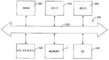
도 9는 본 발명의 일 실시예의 시스템을 보여주는 도면이다.9 illustrates a system of one embodiment of the present invention.
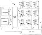
도 1은 상 변화 메모리(phase change memory. 이하, "PCM"이라 함) 디바이스(1)를 보여준다. 다수의 PCM 셀(2)들이 행과 열로 배치되어 어레이(3)를 형성하게 된다. 행 디코더(ROW DEC; 4) 및 열 디코더(COL DEC; 5)는 독출/기입 유닛(R/W; 7)와 결합되며, 독출/기입 유닛(7)은 프로그래밍 회로(PROGRAM; 7a) 및 검증 회로(VERIFY; 7b)를 포함한다. 워드 라인들(WL; 8)과 비트 라인들(9)은, 각각 행들과 열들에 평행하게 배치되고, 공지의 방식으로, 행 디코더(4)와 열 디코더(5)를 통하여 독출/기입 유닛(7)에 선택적으로 접속될 수 있다.1 shows a phase change memory (hereinafter referred to as "PCM")
PCM 셀(2)들은 워드 라인(8)과 비트 라인(9)의 교점에 접속되어 있고, 상 변화 타입의 메모리 소자(10) 및 선택 소자(11)를 포함한다. 메모리 소자(10)는, 대응되는 비트 라인(9)에 접속된 제 1 단자 및 선택 소자(11)의 제 1 단자에 접속된 제 2 단자를 지닌다. 선택 소자(11)는 접지된 제 2 단자 및 워드 라인(8)에 접속된 제어 단자를 지닌다. 다른 실시예에 따르면, 각각의 PCM 셀(2)을 구성하는 메모리 소자(10) 및 선택 소자(11)는 위치를 서로 바꾸는 것이 가능하며, 더욱이, 선택 소자(11)들은 단지 2 개의 단자들을 지닐 수 있다(예컨대 다이오드들).The
프로그래밍 회로(7a)는, 아래에 설명되는 프로그래밍 방법에 따라서, 초기화 펄스들(PI) 및 프로그래밍 펄스들(PR, PP0, PPK)을 선택된 PCM 셀(2)들에 제공하도록 구성된다. 상기 펄스들은 전류 펄스들일 수도 있고 전압 펄스들일 수도 있다. 검증 회로(7b)는, (예컨대 각 프로그래밍 펄스 후에,) 저장된 정보를 독출하기 위하여 선택된 PCM 셀(2)들에 접속된다.The
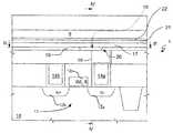
도 2에는 PCM 셀(2)의 단면도가 예시되어 있다. 여기서 설명되는 실시예에서, 선택 소자(11)는 MOS 트랜지스터이지만 다른 선택 소자(예컨대, 바이폴라 트랜지스터)들이 사용될 수 있다. MOS 트랜지스터(11)는 드레인 영역(12a), 소스 영역(12b), 게이트 영역(12c), 드레인 접점(14a) 및 소스 접점(14b)을 각각 포함한다. 드레인(12a) 및 소스(12b)는 N+ 주입물(implant)들로 형성된다. 게이트(12c)는 폴리실리콘으로 형성되고 (P-형) 반도체 기판(18) 상에 확장되어 있으며 (P-형) 반도체 기판(18)으로부터 절연되어 있다. 게이트(12c)는 워드 라인(8)에 접속되고, 구동될 때에는, 드레인(12a) 및 소스(12b) 간에 도전 채널을 생성함으로써 트랜지스터를 턴온시킨다. MOS 트랜지스터는 포화 상태가 되어 전압-제어형 전류원(voltage-controlled current-source) 선택기로서 사용될 수 있다.2 is a cross-sectional view of the
컵 형상의 발열 소자(16)는 드레인 접점(14a) 상에 형성된다. 발열 소자의 상부는 도 3에 또한 도시된 바와 같이 서브리소그래픽 두께(sublithographic thickness)를 갖는 원형 또는 타원형의 벽에 의하여 한정된다. 여기서, "서브리소그래픽"이란 용어는, 현재의 광(UV) 리소그래픽 기술들로 달성될 수 있는 최소 치수(minimum dimension)보다 작은 선형 치수(linear dimension)로서, 100nm보다 작은 치수, 바람직하게는 50-60mn에서 대략 5-20nm에 이르기까지의 치수를 의미한다. 예를 들어 GST와 같은 칼코겐 물질의 스트립(17)은 비트 라인(9)들에 평행하게 배치되고, 예를 들어 질소 화합물(nitride)과 같은 미니트렌치 층(minitrench layer; 19)에 의해 발열 소자(16)와 분리된다. 또한, 캡 층(cap layer; 21) 및 장벽 층(barrier layer; 22)이 스트립(17) 및 비트 라인(9)들 사이에 평행하게 배치된다. 연장된 미니트렌치(20; 또한 도 3 참조)는 비트 라인(9)들과 평행한 방향으로 발열 소자(16)의 상측에서 발열 소자(16)를 가로지르는 미니트렌치 층(19)을 관통하여 형성된다. 따라서, 도 4에 도시된 바와 같이, 스트립(17)의 얇은 부분(17a)은 미니트렌치(20)를 충전(充塡)하여 발열 소자(16)와 접촉하게 된다. 미니트렌치(20)는 하측 방향으로, 워드 라인(8)들과 평행한 방향으로 서브리소그래픽 폭(sublithographic width)을 지니고, 그 결과 스트립(17)의 얇은 부분(17a)과 발열 소자(16) 사이의 접촉 영역도 서브리소그래픽 면적(sublithographic extension)을 지닌다. PCM의 셀(2)의 메모리 소자(10)는, 상기 접촉 영역에서 스트립(17)의 얇은 부분(17a) 내에 형성된다. 상기 접촉 영역의 서브리소그래픽 면적 때문에, 스트립(17) 및 발열 소자(16)를 통해 흐르는 전류가 비교적 적더라도, 주울(Joule) 효과에 의해 메모리 소자(10)에 상응하는 분량의 상 전이들을 야기시키기에 충분한 열이 생기게 된다.The cup-shaped
특히, 적은 양의 전류는 미니트렌치(20) 내에 평균 직경(D)을 갖는 퍼콜레이션 통로(percolation path; 25)를 생성하는데 사용될 수 있다. 퍼콜레이션 통로(25)는, 비정질 상태에 있는 상 변화 물질(27)을 관통하는 결정질 통로(crystalline path)이다. 따라서, 퍼콜레이션 통로(25)는, 얇은 부분(17a) 내에서 발열 소자(16)에서부터 스트립(17)에 이르기까지 연속적으로 통과한다. 일단 퍼콜레이션 통로(25)가 형성되면, 이하에서 부연 설명되는 바와 같이, 그 통로의 직경을 확장시키기 위해서는 진폭이 증가된 펄스가 사용될 수 있다. PCM 셀(2)들에 저장된 정보는 메모리 소자(10)들을 형성하는 칼코겐 물질의 소정 저항값 레벨들(프로그래밍 상태들)에 관련된다. 따라서, 퍼콜레이션 통로(25)의 직경을 변하게 함으로써, 그에 대응해서 저항값 레벨들이 변하게 될 수 있다. 특정 저항값 레벨들 및 범위들은 적용예에 따라서 달라지게 된다. 예컨대, 디바이스들의 등방성 스케일링(isotrophic scaling)은 메모리 소자(10)들의 치수(dimension)들을 감소시켜 주며 그에 대응해서 메모리 소자들의 저항값 레벨들을 상응하도록 증가시켜 준다.In particular, a small amount of current can be used to create a
모든 PCM 셀(2)들은, 이들의 프로그래밍 특성들의 변동(variability)을 최소화하기 위해, 제조 후에 한번 초기화될 수 있다. 이러한 목적으로, 프로그래밍 회로(7a)는 PCM 셀(2)들에 단일의 초기화 펄스(PI)를 공급하는데, 단일의 초기화 펄스(PI)는 메모리 소자(10)들의 칼코겐 물질을 우선적으로 완전히 리세트된 상태로 되게 한 다음에 다시 완전히 세트된 상태로 되게 할 정도의 진폭 및 지속시간을 갖는다. 따라서, 칼코겐 물질은 균일해 지고, 가능한 불규칙성들은 제거된다. 초기화 펄스(PI)는 칼코겐 물질을 천천히 냉각시킬 수 있게 하는 경사 전류 또는 전압 펄스(current or voltage sloped pulse)일 수 있다. 또는 계단 형상으로 감소하는 경사 펄스(decreasing stepped ramp)도 채택될 수 있다.All
도 5는 4-상태 PCM 셀(당업계에 잘 알려져 있는 바와 같이, 전류 범위들을 부가적으로 분할함으로써 추가적인 상태들이 추가될 수 있음)의 전류(IREAD/IMAX) 대 확률 밀도(probability density)를 나타낸 도면이다. 중간 레벨들 "01" 및 "10"에 더 많은 마진(margin)을 허용하기 위해, "00(비정질)" 및 "11(결정질)"을 포함하는 프로그래밍 범위 전체를 사용하는 것이 바람직하다. 이 경우에, "00"은 리세트 비트들와 관련이 있는 비정질 상태이다. 리세트(reset)는 통상적으로, 칼코겐 화합물 재료를 대략 600℃의 융해점으로 이르게 한 다음에 이를 급격하게 냉각시키는 단일의 방형파 펄스(single square pulse)(예컨대, 50ns)에 의해서 얻어진다. 레벨 "11"은 모든 결정질 상태에서의 세트 비트들에 관련된다. 세트(set)는 통상적으로, 칼코겐 화합물 재료를 결정화 온도(crystallization temperature)(예컨대 400℃) 까지 이르게 한 다음에 이를, 장거리 질서(long-range order)가 재구축될 때까지 그 온도에서 유지하는 단일의 방형파 펄스(single square pulse)에 의해서 얻어진다. 또는, 세트(set)는 칼코겐 화합물 재료를 융해점에 이르게 한 다음에 이를, 결정(crystal)들이 재구성하기에 충분할 정도로 천천히 냉각시킴으로써 얻어질 수 있다.5 shows the current (IREAD / IMAX ) vs. probability density of a four-state PCM cell (additional states can be added by additionally dividing the current ranges, as is well known in the art). The figure which shows. In order to allow more margin at intermediate levels "01" and "10", it is desirable to use the entire programming range including "00 (amorphous)" and "11 (crystalline)". In this case, "00" is the amorphous state associated with the reset bits. Reset is typically obtained by a single square pulse (e.g., 50 ns) which leads the chalcogenide material to a melting point of approximately 600 DEG C and then rapidly cools it. Level "11" relates to set bits in all crystalline states. Sets typically bring the chalcogenide material up to a crystallization temperature (eg 400 ° C.) and then maintain it at that temperature until a long-range order is reestablished. Obtained by a single square pulse. Alternatively, a set can be obtained by bringing the chalcogenide material to the melting point and then cooling it slowly enough to crystallize.
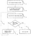
2 가지의 중간 상태들("01", "10")을 획득하기 위해서는 일반적으로 프로그래밍 펄스들이 추가되거나 퍼콜레이션 통로가 생성될 필요가 있다. 중간 상태들의 프로그래밍은 도 6을 참조하여 좀더 상세하게 설명된다. 도 6에서는, 프로세스 블럭 70에서, PCM을 비정질 상태 "00"에 있게 하기 위해서 리세트 펄스(PR)가 인가된다. 그후에, 프로그래밍 회로(7a)는 시작 프로그래밍 펄스(PP0) 및 하나 이상의 조정 프로그래밍 펄스(PPK)들을 공급하도록 구성된다. 프로세스 블럭 72에서, 시작 프로그래밍 펄스(PP0)는 추정 직경(D)의 퍼콜레이션 통로를 생성하여, 전류 레벨들을, 원하는 프로그래밍에 따라서 "01" 범위의 시점(50)(도 5 참조) 또는 "10" 범위의 시점(52)(도 5 참조)에 이르게 한다. 이러한 제1 퍼콜레이션 펄스(first percolation pulse)는 전형적인 결정화 전류들(crystallization currents)보다 대략 5 배 정도 낮은 고정 전류에 의하여 인가된다. 그러나, 전류 레벨들(50, 52)은 원하는 전류 레벨들이 아니다. 오히려, 그들은 PCM을, 도 5에서 곡선들 아래에 속하는 타깃(target) 전류 레벨들(54, 56)에 이르게 하는 시점을 나타낸 것이다. 프로세스 블럭 74에서, 검증 회로(7b)는 PCM 셀의 전류를 독출하고 그 전류가 원하는 범위들(도 5에서 54 및 56) 내에 있는 지를 판단한다. 이를 실행하기 위해서, 검증 회로(7b)는 소정의 전압을 인가하여 선택된 PCM 셀(2)들을 통해 흐르는 전류들을 비교한다.In order to obtain two intermediate states ("01", "10"), programming pulses generally need to be added or a percolation path needs to be created. Programming of intermediate states is described in more detail with reference to FIG. 6. In FIG. 6, at
결정 블럭 76에서, 독출 전류가 원하는 범위(즉, "01"에 대해 54, "10"에 대해 56) 내에 있는 지에 대한 결정이 내려진다. 독출 전류가 원하는 레벨보다 낮으면, 프로세스 블럭 78에서 프로그래밍 회로(7a)는 이전에 인가된 펄스에 비해서 폭은 같고 진폭은 증가된 펄스를 인가한다. 진폭이 증가된 펄스가 인가되면 퍼콜레이션 통로의 직경이 증가하게 된다. 화살표 79로 도시된 바와 같이, 폭이 고정되고 진폭이 증가된 펄스들로 프로세스 블럭들 74, 76 및 78이 다시 반복된다. 이러한 반복은 독출 전류들이 요구되는 오차 범위(tolerance)들 내에 속한다고 검증 회로(7b)가 결정할 때까지 계속된다. 독출 전류들이 요구되는 오차 범위들 내에 속한다고 검증 회로(7b)가 결정하면, 결정 블럭 76은 긍정(YES)으로 응답하게 되고, 프로그래밍은 프로세스 블럭 80에서 완료된다. 다른 실시예에서는, 진폭이 고정되고 폭이 증가된 펄스들이 사용될 수 있다.At
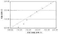
도 7은 프로그래밍 전류와 독출 전류 간의 선형 관계를 보여주는 도면이다. 프로그래밍 전류의 진폭을 증가시키면 퍼콜레이션 통로의 직경 또는 폭이 넓어지고 그에 따라 독출 전류가 증가하게 된다.7 shows a linear relationship between programming current and read current. Increasing the amplitude of the programming current increases the diameter or width of the percolation path, thereby increasing the read current.
도 8은 본 발명의 장점들 중의 하나를 보여주는 도면이다. 특히, 퍼콜레이션 통로는 저항값 변동의 감소를 초래한다. 퍼콜레이션 통로는, 칼코겐 물질을 통한 병렬의 전류 통로로서 효율적으로 임의의 직렬 전류 성분이 나타나지 않게 한다. 이 도면에서는, 퍼콜레이션 통로의 변동 성분의 프로트(plot) 선도(線圖)가 삼각형 플로트 점들로 나타나 있으며, 다이어몬드형 플로트 점들로 나타나 있는 직렬 통로는 보다 높은 저항값 변동을 초래한다.8 illustrates one of the advantages of the present invention. In particular, the percolation passage results in a reduction in resistance value variation. The percolation path is a parallel current path through the chalcogenide that effectively prevents any series of current components from appearing. In this figure, the plot plot of the variation component of the percolation passage is represented by triangular float points, and the series passage represented by diamond float points results in a higher resistance value variation.
도 9는 본 발명의 한 실시예에 따른 시스템(500)의 일부를 보여준다. 시스템(500)은 무선 장치들, 예컨대, PDA(personal digital assistant), 무선 기능을 갖는 랩탑(laptop) 또는 휴대용 컴퓨터, 웹 태블릿(web tablet), 무선 전화, 페이져(pager), 인스턴트 메시징 장치(instant messaging device), 디지털 음악 재생기(digital music player), 디지털 카메라, 또는 무선으로 정보를 송신 또는 수신할 수도 있고 무선으로 정보를 송신 및 수신할 수 있는 다른 장치들에 사용될 수 있다. 시스템(500)은 WLAN(wireless local area network) 시스템, WPAN(wireless personal area network) 시스템, 또는 셀룰러 네트워크와 같은 시스템들 중의 어느 하나에도 사용될 수 있다. 그러나, 이러한 태양으로만 본 발명의 범위가 한정되는 것은 아니다.9 shows a portion of a
시스템(500)은 제어기(510); 예컨대 키패드(keypad)나 디스플레이와 같은 입력/출력(I/O) 장치(520); 상 변화 메모리 디바이스(1); 무선 인터페이스(540); 및 SRAM(static random access memory. 560);을 포함할 수 있으며 이들 각각이 버스(550)를 통해 결합되어 있다. 한 실시예에서, 배터리(580)는 전력(power)을 시스템(500)에 공급할 수 있다. 그러나, 본 발명의 범위가 위와 같은 구성 요소들의 일부 또는 전부를 가지는 실시예들로만 한정되는 것은 아니다.
제어기(510)는, 예컨대, 1 개 이상의 마이크로 프로세서들, 디지털 신호 처리기들, 마이크로 컨트롤러들 등을 구비할 수 있다. 상 변화 메모리 디바이스(MEMORY; 1)는 시스템(500)이 전송하거나 전송받는 메시지들을 저장하는데 사용될 수 있다. 또한, 상 변화 메모리 디바이스(1)는 선택적으로 시스템(500)의 작동 중에 제어기(510)에 의하여 실행되는 명령어들을 저장하는데 사용될 수도 있고, 사용자 데이터를 저장하는데 사용될 수도 있다. 명령어들은 디지털 정보로서 저장될 수 있다. 사용자 데이터는, 본 명세서에 기재된 바와 같이, 메모리의 한 섹션(section)에 디지털 정보로서 저장될 수 있고, 다른 섹션에 아날로그 데이터로서 저장될 수 있다. 또 다른 예로서, 소정 섹션은 한 시기에 라벨링(labeling)되어 디지털 정보를 저장할 수 있고, 그 다음에 다시 라벨링되어 아날로그 정보를 저장하도록 구성될 수 있다.
입력/출력 장치(520)는 메시지를 생성하는데 사용될 수 있다. 시스템(500)은 무선 인터페이스(540)를 사용하여 RF 신호(radio frequency signal)를 가지고 무선 통신 네트워크로 메시지들을 전송하거나 무선 통신 네트워크로부터 메시지들을 수신할 수 있다. 무선 인터페이스(540)의 예들에는 다이폴 안테나(dipole antenna)와 같은 안테나 또는 무선 트랜시버(wireless transceiver)가 있을 수 있으나, 본 발명의 범위는 이러한 태양으로만 한정되지 않는다. 또한, 입력/출력 장치(520)는 디지털 출력(디지털 정보가 저장된 경우에) 또는 아날로그 정보(아날로그 정보가 저장된 경우)로서 저장된 것을 반영하는 전압을 공급할 수 있다.The input /
위에서는 무선 응용예와 관련된 실시예가 제공되었으나, 본 발명의 실시예들은 비무선(non-wireless) 응용예들에서도 사용될 수 있다.While embodiments related to wireless applications have been provided above, embodiments of the present invention may also be used in non-wireless applications.
마지막으로, 다양한 변형들과 수정들이 본 명세서에 기재되고 도시된 프로그래밍 방법 및 상 변화 메모리 디바이스에 대해 이루어질 수 있으며, 그러한 모든 변형들과 수정들은 첨부된 청구항들에 의하여 규정된 발명의 범위에 속한다. 특히, 본 발명은 위에 기재된 PCM 셀 구조로만 한정되지는 않는다. 어떤 유형의 선택 소자들 및 메모리 소자들도 사용될 수 있고, 벽(wall) 형상의 발열 소자들, 랜스(lance) 형상의 발열 소자들 등과 같은 임의의 적합한 발열 소자들도 사용될 수 있다.Finally, various variations and modifications may be made to the programming method and phase change memory device described and shown herein, all such variations and modifications being within the scope of the invention as defined by the appended claims. In particular, the present invention is not limited to the PCM cell structure described above. Any type of selection elements and memory elements may be used, and any suitable heating elements may be used, such as wall shaped heating elements, lance shaped heating elements, and the like.
Claims (15)
Translated fromKoreanApplications Claiming Priority (2)
| Application Number | Priority Date | Filing Date | Title |
|---|---|---|---|
| EP05104877AEP1729303B1 (en) | 2005-06-03 | 2005-06-03 | Method for multilevel programming of phase change memory cells using a percolation algorithm |
| EP05104877.5 | 2005-06-03 |
Publications (2)
| Publication Number | Publication Date |
|---|---|
| KR20080021688A KR20080021688A (en) | 2008-03-07 |
| KR101263360B1true KR101263360B1 (en) | 2013-05-21 |
Family
ID=35406273
Family Applications (1)
| Application Number | Title | Priority Date | Filing Date |
|---|---|---|---|
| KR1020077030076AActiveKR101263360B1 (en) | 2005-06-03 | 2006-06-01 | Method for multilevel programming of phase change memory cells using a percolation algorithm |
Country Status (7)
| Country | Link |
|---|---|
| US (1) | US7639526B2 (en) |
| EP (3) | EP1729303B1 (en) |
| JP (1) | JP2008546124A (en) |
| KR (1) | KR101263360B1 (en) |
| CN (1) | CN101238523B (en) |
| DE (1) | DE602005025323D1 (en) |
| WO (1) | WO2006128896A1 (en) |
Families Citing this family (75)
| Publication number | Priority date | Publication date | Assignee | Title |
|---|---|---|---|---|
| US20070025166A1 (en)* | 2005-07-27 | 2007-02-01 | Spansion Llc | Program/erase waveshaping control to increase data retention of a memory cell |
| DE602006012825D1 (en) | 2006-07-27 | 2010-04-22 | St Microelectronics Srl | Phase change memory device |
| US8116117B2 (en) | 2006-11-29 | 2012-02-14 | Samsung Electronics Co., Ltd. | Method of driving multi-level variable resistive memory device and multi-level variable resistive memory device |
| KR100801082B1 (en)* | 2006-11-29 | 2008-02-05 | 삼성전자주식회사 | Method of driving multilevel variable resistance memory device and multilevel variable resistance memory device |
| JP2008218492A (en)* | 2007-02-28 | 2008-09-18 | Elpida Memory Inc | Phase change memory device |
| US7577023B2 (en)* | 2007-05-04 | 2009-08-18 | Qimonda North America Corp. | Memory including write circuit for providing multiple reset pulses |
| KR100909770B1 (en)* | 2007-08-10 | 2009-07-29 | 주식회사 하이닉스반도체 | Driving Method of Phase Change Memory Device |
| KR100905170B1 (en)* | 2007-08-10 | 2009-06-29 | 주식회사 하이닉스반도체 | Driving Method of Phase Change Memory Device |
| JP5172269B2 (en) | 2007-10-17 | 2013-03-27 | 株式会社東芝 | Nonvolatile semiconductor memory device |
| US7961507B2 (en) | 2008-03-11 | 2011-06-14 | Micron Technology, Inc. | Non-volatile memory with resistive access component |
| JP2009266316A (en)* | 2008-04-25 | 2009-11-12 | Semiconductor Technology Academic Research Center | Memory device, electronic equipment, recording method for phase change memory device |
| US8134857B2 (en)* | 2008-06-27 | 2012-03-13 | Macronix International Co., Ltd. | Methods for high speed reading operation of phase change memory and device employing same |
| US8076208B2 (en)* | 2008-07-03 | 2011-12-13 | Micron Technology, Inc. | Method for forming transistor with high breakdown voltage using pitch multiplication technique |
| US8031517B2 (en) | 2008-07-30 | 2011-10-04 | Samsung Electronics Co., Ltd. | Memory device, memory system having the same, and programming method of a memory cell |
| IT1392578B1 (en)* | 2008-12-30 | 2012-03-09 | St Microelectronics Rousset | MULTILEVEL PROGRAMMING METHOD OF MEMORY CELLS AT USING PHASE OF CHANGING ADAPTIVE RESET PULSES |
| KR101057725B1 (en)* | 2008-12-31 | 2011-08-18 | 주식회사 하이닉스반도체 | Multi-level cell data sensing device and method thereof |
| US8107283B2 (en)* | 2009-01-12 | 2012-01-31 | Macronix International Co., Ltd. | Method for setting PCRAM devices |
| US7929338B2 (en)* | 2009-02-24 | 2011-04-19 | International Business Machines Corporation | Memory reading method for resistance drift mitigation |
| US8331168B2 (en) | 2009-04-30 | 2012-12-11 | International Business Machines Corporation | Increased capacity heterogeneous storage elements |
| US8470635B2 (en)* | 2009-11-30 | 2013-06-25 | Micron Technology, Inc. | Keyhole-free sloped heater for phase change memory |
| WO2011074021A1 (en) | 2009-12-18 | 2011-06-23 | Mattia Boniardi | Modified reset state for enhanced read margin of phase change memory |
| US9196530B1 (en) | 2010-05-19 | 2015-11-24 | Micron Technology, Inc. | Forming self-aligned conductive lines for resistive random access memories |
| US9224496B2 (en) | 2010-08-11 | 2015-12-29 | Shine C. Chung | Circuit and system of aggregated area anti-fuse in CMOS processes |
| US9251893B2 (en) | 2010-08-20 | 2016-02-02 | Shine C. Chung | Multiple-bit programmable resistive memory using diode as program selector |
| US8804398B2 (en) | 2010-08-20 | 2014-08-12 | Shine C. Chung | Reversible resistive memory using diodes formed in CMOS processes as program selectors |
| US9019742B2 (en) | 2010-08-20 | 2015-04-28 | Shine C. Chung | Multiple-state one-time programmable (OTP) memory to function as multi-time programmable (MTP) memory |
| US9824768B2 (en) | 2015-03-22 | 2017-11-21 | Attopsemi Technology Co., Ltd | Integrated OTP memory for providing MTP memory |
| US8488364B2 (en) | 2010-08-20 | 2013-07-16 | Shine C. Chung | Circuit and system of using a polysilicon diode as program selector for resistive devices in CMOS logic processes |
| US9711237B2 (en) | 2010-08-20 | 2017-07-18 | Attopsemi Technology Co., Ltd. | Method and structure for reliable electrical fuse programming |
| US8830720B2 (en) | 2010-08-20 | 2014-09-09 | Shine C. Chung | Circuit and system of using junction diode as program selector and MOS as read selector for one-time programmable devices |
| US9496033B2 (en) | 2010-08-20 | 2016-11-15 | Attopsemi Technology Co., Ltd | Method and system of programmable resistive devices with read capability using a low supply voltage |
| US9818478B2 (en) | 2012-12-07 | 2017-11-14 | Attopsemi Technology Co., Ltd | Programmable resistive device and memory using diode as selector |
| US9070437B2 (en) | 2010-08-20 | 2015-06-30 | Shine C. Chung | Circuit and system of using junction diode as program selector for one-time programmable devices with heat sink |
| US9460807B2 (en) | 2010-08-20 | 2016-10-04 | Shine C. Chung | One-time programmable memory devices using FinFET technology |
| US9236141B2 (en) | 2010-08-20 | 2016-01-12 | Shine C. Chung | Circuit and system of using junction diode of MOS as program selector for programmable resistive devices |
| US9431127B2 (en) | 2010-08-20 | 2016-08-30 | Shine C. Chung | Circuit and system of using junction diode as program selector for metal fuses for one-time programmable devices |
| US10249379B2 (en) | 2010-08-20 | 2019-04-02 | Attopsemi Technology Co., Ltd | One-time programmable devices having program selector for electrical fuses with extended area |
| US10916317B2 (en) | 2010-08-20 | 2021-02-09 | Attopsemi Technology Co., Ltd | Programmable resistance memory on thin film transistor technology |
| US10923204B2 (en) | 2010-08-20 | 2021-02-16 | Attopsemi Technology Co., Ltd | Fully testible OTP memory |
| US9042153B2 (en) | 2010-08-20 | 2015-05-26 | Shine C. Chung | Programmable resistive memory unit with multiple cells to improve yield and reliability |
| US10229746B2 (en) | 2010-08-20 | 2019-03-12 | Attopsemi Technology Co., Ltd | OTP memory with high data security |
| US9025357B2 (en) | 2010-08-20 | 2015-05-05 | Shine C. Chung | Programmable resistive memory unit with data and reference cells |
| US8488359B2 (en) | 2010-08-20 | 2013-07-16 | Shine C. Chung | Circuit and system of using junction diode as program selector for one-time programmable devices |
| US8913449B2 (en) | 2012-03-11 | 2014-12-16 | Shine C. Chung | System and method of in-system repairs or configurations for memories |
| US8988965B2 (en) | 2010-11-03 | 2015-03-24 | Shine C. Chung | Low-pin-count non-volatile memory interface |
| US9076513B2 (en) | 2010-11-03 | 2015-07-07 | Shine C. Chung | Low-pin-count non-volatile memory interface with soft programming capability |
| US9019791B2 (en) | 2010-11-03 | 2015-04-28 | Shine C. Chung | Low-pin-count non-volatile memory interface for 3D IC |
| US9496265B2 (en)* | 2010-12-08 | 2016-11-15 | Attopsemi Technology Co., Ltd | Circuit and system of a high density anti-fuse |
| US8848423B2 (en) | 2011-02-14 | 2014-09-30 | Shine C. Chung | Circuit and system of using FinFET for building programmable resistive devices |
| US10586832B2 (en) | 2011-02-14 | 2020-03-10 | Attopsemi Technology Co., Ltd | One-time programmable devices using gate-all-around structures |
| US10192615B2 (en) | 2011-02-14 | 2019-01-29 | Attopsemi Technology Co., Ltd | One-time programmable devices having a semiconductor fin structure with a divided active region |
| US9324849B2 (en) | 2011-11-15 | 2016-04-26 | Shine C. Chung | Structures and techniques for using semiconductor body to construct SCR, DIAC, or TRIAC |
| US9136261B2 (en) | 2011-11-15 | 2015-09-15 | Shine C. Chung | Structures and techniques for using mesh-structure diodes for electro-static discharge (ESD) protection |
| US8912576B2 (en) | 2011-11-15 | 2014-12-16 | Shine C. Chung | Structures and techniques for using semiconductor body to construct bipolar junction transistors |
| US8917533B2 (en) | 2012-02-06 | 2014-12-23 | Shine C. Chung | Circuit and system for testing a one-time programmable (OTP) memory |
| US9007804B2 (en) | 2012-02-06 | 2015-04-14 | Shine C. Chung | Circuit and system of protective mechanisms for programmable resistive memories |
| US8861249B2 (en) | 2012-02-06 | 2014-10-14 | Shine C. Chung | Circuit and system of a low density one-time programmable memory |
| US20140071747A1 (en) | 2012-09-07 | 2014-03-13 | Being Advanced Memory Corporation | Processors and Systems with Multicell Multibit Phase-Change Memory |
| US9076526B2 (en) | 2012-09-10 | 2015-07-07 | Shine C. Chung | OTP memories functioning as an MTP memory |
| US9183897B2 (en) | 2012-09-30 | 2015-11-10 | Shine C. Chung | Circuits and methods of a self-timed high speed SRAM |
| US9324447B2 (en) | 2012-11-20 | 2016-04-26 | Shine C. Chung | Circuit and system for concurrently programming multiple bits of OTP memory devices |
| US8988926B2 (en) | 2013-01-11 | 2015-03-24 | Micron Technology, Inc. | Method, system and device for phase change memory with shunt |
| KR102079370B1 (en) | 2013-02-05 | 2020-02-20 | 삼성전자주식회사 | Nonvolatile memory device and writing method thereof |
| KR20140117893A (en)* | 2013-03-27 | 2014-10-08 | 인텔렉추얼디스커버리 주식회사 | Phase-change memory device and method for multi-level programing of phase-change memory device |
| US9412473B2 (en) | 2014-06-16 | 2016-08-09 | Shine C. Chung | System and method of a novel redundancy scheme for OTP |
| US10726914B2 (en) | 2017-04-14 | 2020-07-28 | Attopsemi Technology Co. Ltd | Programmable resistive memories with low power read operation and novel sensing scheme |
| US10535413B2 (en) | 2017-04-14 | 2020-01-14 | Attopsemi Technology Co., Ltd | Low power read operation for programmable resistive memories |
| US11062786B2 (en) | 2017-04-14 | 2021-07-13 | Attopsemi Technology Co., Ltd | One-time programmable memories with low power read operation and novel sensing scheme |
| US11615859B2 (en) | 2017-04-14 | 2023-03-28 | Attopsemi Technology Co., Ltd | One-time programmable memories with ultra-low power read operation and novel sensing scheme |
| US10770160B2 (en) | 2017-11-30 | 2020-09-08 | Attopsemi Technology Co., Ltd | Programmable resistive memory formed by bit slices from a standard cell library |
| CN109991360B (en)* | 2017-12-14 | 2023-04-21 | 特利丹菲力尔探测公司 | Retaining deformable memory material in a flow path |
| US12154001B2 (en) | 2019-03-15 | 2024-11-26 | International Business Machines Corporation | Parameter extrapolation in quantum variational circuits |
| IT201900021606A1 (en) | 2019-11-19 | 2021-05-19 | St Microelectronics Srl | PHASE CHANGE MEMORY DEVICE AND METHOD OF PROGRAMMING A PHASE CHANGE MEMORY DEVICE |
| US11164628B2 (en) | 2020-02-21 | 2021-11-02 | International Business Machines Corporation | Compensating PCM drift for neuromorphic applications |
| US11283015B2 (en) | 2020-03-24 | 2022-03-22 | International Business Machines Corporation | Projected phase change memory devices |
Citations (1)
| Publication number | Priority date | Publication date | Assignee | Title |
|---|---|---|---|---|
| JP3454821B2 (en) | 1991-08-19 | 2003-10-06 | エナージー・コンバーション・デバイセス・インコーポレーテッド | Electrically erasable, directly overwritable, multi-bit single-cell memory elements and arrays made therefrom |
Family Cites Families (12)
| Publication number | Priority date | Publication date | Assignee | Title |
|---|---|---|---|---|
| US3886577A (en)* | 1973-09-12 | 1975-05-27 | Energy Conversion Devices Inc | Filament-type memory semiconductor device and method of making the same |
| US3922648A (en)* | 1974-08-19 | 1975-11-25 | Energy Conversion Devices Inc | Method and means for preventing degradation of threshold voltage of filament-forming memory semiconductor device |
| CA1322258C (en) | 1988-01-19 | 1993-09-14 | Thomas S. Buzak | Apparatus for and methods of addressing data storage elements |
| US5825046A (en) | 1996-10-28 | 1998-10-20 | Energy Conversion Devices, Inc. | Composite memory material comprising a mixture of phase-change memory material and dielectric material |
| US7365354B2 (en)* | 2001-06-26 | 2008-04-29 | Ovonyx, Inc. | Programmable resistance memory element and method for making same |
| DE60137788D1 (en) | 2001-12-27 | 2009-04-09 | St Microelectronics Srl | Architecture of a non-volatile phase change memory matrix |
| US6625054B2 (en)* | 2001-12-28 | 2003-09-23 | Intel Corporation | Method and apparatus to program a phase change memory |
| US6512241B1 (en)* | 2001-12-31 | 2003-01-28 | Intel Corporation | Phase change material memory device |
| US6813177B2 (en)* | 2002-12-13 | 2004-11-02 | Ovoynx, Inc. | Method and system to store information |
| DE60323202D1 (en)* | 2003-02-21 | 2008-10-09 | St Microelectronics Srl | Phase change memory device |
| US7085154B2 (en)* | 2003-06-03 | 2006-08-01 | Samsung Electronics Co., Ltd. | Device and method for pulse width control in a phase change memory device |
| KR100618855B1 (en)* | 2004-08-02 | 2006-09-01 | 삼성전자주식회사 | Metal contact structure formation method and phase change memory manufacturing method using the same |
- 2005
- 2005-06-03EPEP05104877Apatent/EP1729303B1/ennot_activeExpired - Lifetime
- 2005-06-03EPEP10171507Apatent/EP2309516A1/ennot_activeWithdrawn
- 2005-06-03EPEP10173621.3Apatent/EP2249351B1/ennot_activeExpired - Lifetime
- 2005-06-03DEDE602005025323Tpatent/DE602005025323D1/ennot_activeExpired - Lifetime
- 2006
- 2006-06-01CNCN2006800286197Apatent/CN101238523B/enactiveActive
- 2006-06-01KRKR1020077030076Apatent/KR101263360B1/enactiveActive
- 2006-06-01JPJP2008514105Apatent/JP2008546124A/enactivePending
- 2006-06-01WOPCT/EP2006/062812patent/WO2006128896A1/enactiveApplication Filing
- 2007
- 2007-12-03USUS11/949,598patent/US7639526B2/enactiveActive
Patent Citations (1)
| Publication number | Priority date | Publication date | Assignee | Title |
|---|---|---|---|---|
| JP3454821B2 (en) | 1991-08-19 | 2003-10-06 | エナージー・コンバーション・デバイセス・インコーポレーテッド | Electrically erasable, directly overwritable, multi-bit single-cell memory elements and arrays made therefrom |
Also Published As
| Publication number | Publication date |
|---|---|
| KR20080021688A (en) | 2008-03-07 |
| CN101238523B (en) | 2012-03-28 |
| US20080151612A1 (en) | 2008-06-26 |
| US7639526B2 (en) | 2009-12-29 |
| EP2249351A1 (en) | 2010-11-10 |
| WO2006128896A1 (en) | 2006-12-07 |
| EP1729303A1 (en) | 2006-12-06 |
| CN101238523A (en) | 2008-08-06 |
| DE602005025323D1 (en) | 2011-01-27 |
| EP1729303B1 (en) | 2010-12-15 |
| EP2309516A1 (en) | 2011-04-13 |
| JP2008546124A (en) | 2008-12-18 |
| EP2249351B1 (en) | 2013-05-01 |
Similar Documents
| Publication | Publication Date | Title |
|---|---|---|
| KR101263360B1 (en) | Method for multilevel programming of phase change memory cells using a percolation algorithm | |
| US7515460B2 (en) | Multilevel programming of phase change memory cells | |
| US10482954B2 (en) | Phase change memory device | |
| US6816404B2 (en) | Architecture of a phase-change nonvolatile memory array | |
| US7787291B2 (en) | Programming a multilevel phase change memory cell | |
| US7864567B2 (en) | Programming a normally single phase chalcogenide material for use as a memory of FPLA | |
| US7701749B2 (en) | Multiple level cell phase-change memory devices having controlled resistance drift parameter, memory systems employing such devices and methods of reading memory devices | |
| US8149616B2 (en) | Method for multilevel programming of phase change memory cells using adaptive reset pulses | |
| US9570169B1 (en) | Resistive memory device | |
| KR100738092B1 (en) | Multi-Bit Operation Method of Phase Transition Memory Device | |
| US7804082B2 (en) | Phase change memory system | |
| US7029978B2 (en) | Controlling the location of conduction breakdown in phase change memories | |
| US20070238225A1 (en) | Phase change memory with improved temperature stability |
Legal Events
| Date | Code | Title | Description |
|---|---|---|---|
| PA0105 | International application | Patent event date:20071224 Patent event code:PA01051R01D Comment text:International Patent Application | |
| PG1501 | Laying open of application | ||
| A201 | Request for examination | ||
| PA0201 | Request for examination | Patent event code:PA02012R01D Patent event date:20110310 Comment text:Request for Examination of Application | |
| E902 | Notification of reason for refusal | ||
| PE0902 | Notice of grounds for rejection | Comment text:Notification of reason for refusal Patent event date:20120808 Patent event code:PE09021S01D | |
| E701 | Decision to grant or registration of patent right | ||
| PE0701 | Decision of registration | Patent event code:PE07011S01D Comment text:Decision to Grant Registration Patent event date:20130212 | |
| GRNT | Written decision to grant | ||
| PR0701 | Registration of establishment | Comment text:Registration of Establishment Patent event date:20130506 Patent event code:PR07011E01D | |
| PR1002 | Payment of registration fee | Payment date:20130507 End annual number:3 Start annual number:1 | |
| PG1601 | Publication of registration | ||
| FPAY | Annual fee payment | Payment date:20160418 Year of fee payment:4 | |
| PR1001 | Payment of annual fee | Payment date:20160418 Start annual number:4 End annual number:4 | |
| FPAY | Annual fee payment | Payment date:20170421 Year of fee payment:5 | |
| PR1001 | Payment of annual fee | Payment date:20170421 Start annual number:5 End annual number:5 | |
| FPAY | Annual fee payment | Payment date:20180418 Year of fee payment:6 | |
| PR1001 | Payment of annual fee | Payment date:20180418 Start annual number:6 End annual number:6 | |
| FPAY | Annual fee payment | Payment date:20190508 Year of fee payment:7 | |
| PR1001 | Payment of annual fee | Payment date:20190508 Start annual number:7 End annual number:7 | |
| PR1001 | Payment of annual fee | Payment date:20200423 Start annual number:8 End annual number:8 | |
| PR1001 | Payment of annual fee | Payment date:20210427 Start annual number:9 End annual number:9 | |
| PR1001 | Payment of annual fee | Payment date:20220503 Start annual number:10 End annual number:10 | |
| PR1001 | Payment of annual fee | Payment date:20240423 Start annual number:12 End annual number:12 |