KR101256850B1 - Microwave plasma processing apparatus - Google Patents
Microwave plasma processing apparatusDownload PDFInfo
- Publication number
- KR101256850B1 KR101256850B1KR1020117022121AKR20117022121AKR101256850B1KR 101256850 B1KR101256850 B1KR 101256850B1KR 1020117022121 AKR1020117022121 AKR 1020117022121AKR 20117022121 AKR20117022121 AKR 20117022121AKR 101256850 B1KR101256850 B1KR 101256850B1
- Authority
- KR
- South Korea
- Prior art keywords
- dielectric
- plate
- dielectric window
- dielectric plate
- window
- Prior art date
- Legal status (The legal status is an assumption and is not a legal conclusion. Google has not performed a legal analysis and makes no representation as to the accuracy of the status listed.)
- Expired - Fee Related
Links
Images


Classifications
- H—ELECTRICITY
- H01—ELECTRIC ELEMENTS
- H01J—ELECTRIC DISCHARGE TUBES OR DISCHARGE LAMPS
- H01J37/00—Discharge tubes with provision for introducing objects or material to be exposed to the discharge, e.g. for the purpose of examination or processing thereof
- H01J37/32—Gas-filled discharge tubes
- H01J37/32009—Arrangements for generation of plasma specially adapted for examination or treatment of objects, e.g. plasma sources
- H01J37/32192—Microwave generated discharge
- H—ELECTRICITY
- H05—ELECTRIC TECHNIQUES NOT OTHERWISE PROVIDED FOR
- H05H—PLASMA TECHNIQUE; PRODUCTION OF ACCELERATED ELECTRICALLY-CHARGED PARTICLES OR OF NEUTRONS; PRODUCTION OR ACCELERATION OF NEUTRAL MOLECULAR OR ATOMIC BEAMS
- H05H1/00—Generating plasma; Handling plasma
- H05H1/24—Generating plasma
- H05H1/46—Generating plasma using applied electromagnetic fields, e.g. high frequency or microwave energy
- C—CHEMISTRY; METALLURGY
- C23—COATING METALLIC MATERIAL; COATING MATERIAL WITH METALLIC MATERIAL; CHEMICAL SURFACE TREATMENT; DIFFUSION TREATMENT OF METALLIC MATERIAL; COATING BY VACUUM EVAPORATION, BY SPUTTERING, BY ION IMPLANTATION OR BY CHEMICAL VAPOUR DEPOSITION, IN GENERAL; INHIBITING CORROSION OF METALLIC MATERIAL OR INCRUSTATION IN GENERAL
- C23C—COATING METALLIC MATERIAL; COATING MATERIAL WITH METALLIC MATERIAL; SURFACE TREATMENT OF METALLIC MATERIAL BY DIFFUSION INTO THE SURFACE, BY CHEMICAL CONVERSION OR SUBSTITUTION; COATING BY VACUUM EVAPORATION, BY SPUTTERING, BY ION IMPLANTATION OR BY CHEMICAL VAPOUR DEPOSITION, IN GENERAL
- C23C16/00—Chemical coating by decomposition of gaseous compounds, without leaving reaction products of surface material in the coating, i.e. chemical vapour deposition [CVD] processes
- C23C16/44—Chemical coating by decomposition of gaseous compounds, without leaving reaction products of surface material in the coating, i.e. chemical vapour deposition [CVD] processes characterised by the method of coating
- C23C16/50—Chemical coating by decomposition of gaseous compounds, without leaving reaction products of surface material in the coating, i.e. chemical vapour deposition [CVD] processes characterised by the method of coating using electric discharges
- C23C16/511—Chemical coating by decomposition of gaseous compounds, without leaving reaction products of surface material in the coating, i.e. chemical vapour deposition [CVD] processes characterised by the method of coating using electric discharges using microwave discharges
- H—ELECTRICITY
- H01—ELECTRIC ELEMENTS
- H01J—ELECTRIC DISCHARGE TUBES OR DISCHARGE LAMPS
- H01J37/00—Discharge tubes with provision for introducing objects or material to be exposed to the discharge, e.g. for the purpose of examination or processing thereof
- H01J37/32—Gas-filled discharge tubes
- H01J37/32009—Arrangements for generation of plasma specially adapted for examination or treatment of objects, e.g. plasma sources
- H01J37/32192—Microwave generated discharge
- H01J37/32211—Means for coupling power to the plasma
- H01J37/3222—Antennas
- H—ELECTRICITY
- H01—ELECTRIC ELEMENTS
- H01J—ELECTRIC DISCHARGE TUBES OR DISCHARGE LAMPS
- H01J37/00—Discharge tubes with provision for introducing objects or material to be exposed to the discharge, e.g. for the purpose of examination or processing thereof
- H01J37/32—Gas-filled discharge tubes
- H01J37/32009—Arrangements for generation of plasma specially adapted for examination or treatment of objects, e.g. plasma sources
- H01J37/32192—Microwave generated discharge
- H01J37/32211—Means for coupling power to the plasma
- H01J37/32238—Windows
- H—ELECTRICITY
- H01—ELECTRIC ELEMENTS
- H01J—ELECTRIC DISCHARGE TUBES OR DISCHARGE LAMPS
- H01J37/00—Discharge tubes with provision for introducing objects or material to be exposed to the discharge, e.g. for the purpose of examination or processing thereof
- H01J37/32—Gas-filled discharge tubes
- H01J37/32431—Constructional details of the reactor
- H01J37/3244—Gas supply means
- H01J37/32449—Gas control, e.g. control of the gas flow
- H—ELECTRICITY
- H01—ELECTRIC ELEMENTS
- H01L—SEMICONDUCTOR DEVICES NOT COVERED BY CLASS H10
- H01L21/00—Processes or apparatus adapted for the manufacture or treatment of semiconductor or solid state devices or of parts thereof
- H01L21/02—Manufacture or treatment of semiconductor devices or of parts thereof
- H01L21/04—Manufacture or treatment of semiconductor devices or of parts thereof the devices having potential barriers, e.g. a PN junction, depletion layer or carrier concentration layer
- H01L21/18—Manufacture or treatment of semiconductor devices or of parts thereof the devices having potential barriers, e.g. a PN junction, depletion layer or carrier concentration layer the devices having semiconductor bodies comprising elements of Group IV of the Periodic Table or AIIIBV compounds with or without impurities, e.g. doping materials
- H01L21/30—Treatment of semiconductor bodies using processes or apparatus not provided for in groups H01L21/20 - H01L21/26
- H01L21/302—Treatment of semiconductor bodies using processes or apparatus not provided for in groups H01L21/20 - H01L21/26 to change their surface-physical characteristics or shape, e.g. etching, polishing, cutting
- H01L21/306—Chemical or electrical treatment, e.g. electrolytic etching
- H01L21/3065—Plasma etching; Reactive-ion etching
- H—ELECTRICITY
- H01—ELECTRIC ELEMENTS
- H01L—SEMICONDUCTOR DEVICES NOT COVERED BY CLASS H10
- H01L21/00—Processes or apparatus adapted for the manufacture or treatment of semiconductor or solid state devices or of parts thereof
- H01L21/02—Manufacture or treatment of semiconductor devices or of parts thereof
- H01L21/04—Manufacture or treatment of semiconductor devices or of parts thereof the devices having potential barriers, e.g. a PN junction, depletion layer or carrier concentration layer
- H01L21/18—Manufacture or treatment of semiconductor devices or of parts thereof the devices having potential barriers, e.g. a PN junction, depletion layer or carrier concentration layer the devices having semiconductor bodies comprising elements of Group IV of the Periodic Table or AIIIBV compounds with or without impurities, e.g. doping materials
- H01L21/30—Treatment of semiconductor bodies using processes or apparatus not provided for in groups H01L21/20 - H01L21/26
- H01L21/31—Treatment of semiconductor bodies using processes or apparatus not provided for in groups H01L21/20 - H01L21/26 to form insulating layers thereon, e.g. for masking or by using photolithographic techniques; After treatment of these layers; Selection of materials for these layers
Landscapes
- Engineering & Computer Science (AREA)
- Physics & Mathematics (AREA)
- Chemical & Material Sciences (AREA)
- Plasma & Fusion (AREA)
- Analytical Chemistry (AREA)
- Organic Chemistry (AREA)
- Computer Hardware Design (AREA)
- Materials Engineering (AREA)
- Mechanical Engineering (AREA)
- Metallurgy (AREA)
- General Chemical & Material Sciences (AREA)
- Condensed Matter Physics & Semiconductors (AREA)
- General Physics & Mathematics (AREA)
- Manufacturing & Machinery (AREA)
- Chemical Kinetics & Catalysis (AREA)
- Microelectronics & Electronic Packaging (AREA)
- Power Engineering (AREA)
- Electromagnetism (AREA)
- Spectroscopy & Molecular Physics (AREA)
- Plasma Technology (AREA)
- Chemical Vapour Deposition (AREA)
- Drying Of Semiconductors (AREA)
Abstract
Translated fromKoreanDescription
Translated fromKorean본 발명은, 마이크로파를 이용하여 생성된 플라즈마에 의해 반도체 웨이퍼, 액정용 기판, 유기 EL 소자 등의 피(被)처리체를 플라즈마 처리하는 마이크로파 플라즈마 처리 장치에 관한 것이다.BACKGROUND OF THE
플라즈마 처리는, 반도체 제조 공정의 에칭, 박막 성막 등의 프로세스에 널리 사용되고 있다. 최근, LSI의 고집적화, 고속화, 소전력화의 관점에서 LSI를 구성하는 반도체의 프로세스 룰(IC의 선폭(線幅))이 더욱 미세화되고 있다. 그러나, 종래로부터 다용되고 있는 평행 평판형이나 유도 결합형의 플라즈마 처리 장치에서는, 전자 온도가 높기 때문에, 기판에 손상을 주어 버린다는 과제가 있다.Plasma processing is widely used for processes, such as etching of a semiconductor manufacturing process and thin film film forming. In recent years, from the viewpoint of high integration, high speed, and low power consumption of LSIs, the process rules (line width of ICs) of semiconductors constituting LSIs have become more fine. However, in the conventional parallel plate type and inductively coupled plasma processing apparatus, since the electron temperature is high, there exists a problem of damaging a board | substrate.
또한, 반도체의 웨이퍼 사이즈도 대구경화되고 있고, 이에 수반하여 대구경의 반도체 웨이퍼에 치우침 없이 균일하게 처리를 행하는 것이 요청되고 있다.In addition, the wafer size of a semiconductor is also large-diameter, and with this, it is requested | required to process uniformly without bias to a large-diameter semiconductor wafer.
그래서 최근, 고밀도이며 저전자 온도의 플라즈마를 균일하게 할 수 있는 RLSA(Radial Line Slot Antenna)를 이용한 마이크로파 플라즈마 처리 장치가 주목받고 있다. 이 마이크로파 플라즈마 처리 장치는, 균일한 마이크로파를 발하도록 배열된 다수의 슬롯을 갖는 평면 형상의 마이크로파 안테나로부터 처리 용기 내로 마이크로파를 방사하고, 마이크로파의 전계에 의해 처리 용기 내의 가스를 전리하여 플라즈마를 여기시키는 것이다. 마이크로파 플라즈마 처리 장치에 의하면, 안테나 바로 아래의 넓은 영역에 높은 플라즈마 밀도를 실현할 수 있기 때문에, 단시간에 균일한 플라즈마 처리를 행하는 것이 가능하다. 게다가, 저전자 온도의 플라즈마를 생성할 수 있기 때문에, 피처리 기판으로의 손상을 적게할 수 있다는 이점도 있다.Recently, a microwave plasma processing apparatus using a radial line slot antenna (RLSA) capable of uniformizing a high density and low electron temperature plasma has attracted attention. This microwave plasma processing apparatus radiates microwaves into a processing vessel from a planar microwave antenna having a plurality of slots arranged to emit uniform microwaves, and ionizes the gas in the processing vessel by an electric field of microwaves to excite the plasma. will be. According to the microwave plasma processing apparatus, since a high plasma density can be realized in a wide area immediately under the antenna, it is possible to perform uniform plasma processing in a short time. In addition, since plasma of low electron temperature can be generated, there is an advantage that damage to the substrate to be processed can be reduced.
도 1에 나타내는 바와 같이, 마이크로파 플라즈마 처리 장치에 있어서, 처리 용기(1)의 천정부의 개구는 유전체창(2)에 의해 막힌다. 유전체창(2)의 위에는 마이크로파 안테나(3)가 놓여진다. 내측 도파관 및 외측 도파관으로 이루어지는 동축 도파관의 단면(斷面) 원환상(圓環狀)의 동축 도파로(4)를 전반(傳搬)한 마이크로파는, 디스크 형상의 유전체판(6)을 방사 방향으로 전반한다. 유전체판(6) 내에서 압축되고, 그리고 공진하는 마이크로파는, 도전 재료로 이루어지는 슬롯판(7)의 슬롯을 투과하고, 유전체창(2)을 통하여 처리 용기(1) 내로 방사된다.As shown in FIG. 1, in the microwave plasma processing apparatus, the opening of the ceiling of the
처리 용기의 유전체창은 처리 용기 내부의 플라즈마에 노출되기 때문에, 유전체창에는 열이 축적된다. 유전체창에 열이 축적되는 것을 방지하기 위해, 특허문헌 1에는, 마이크로파 안테나를 유전체창으로 밀착시켜, 마이크로파 안테나에 설치된 냉각판에 의해 유전체창에 축적된 열을 흡수하는 플라즈마 처리 장치가 개시되어 있다. 특허문헌 1에 기재된 플라즈마 처리 장치에 있어서, 마이크로파 안테나의 슬롯판과 유전체창의 접촉면은, 접촉면에 있어서의 전열성을 향상시키기 위해, 0.8∼0.9atm(608∼684Torr)의 범위 내의 압력으로 유지된다.Since the dielectric window of the processing container is exposed to the plasma inside the processing container, heat is accumulated in the dielectric window. In order to prevent heat from accumulating in the dielectric window,
마이크로파의 전반이나 방사에 영향을 주는 것으로서, 슬롯판 주변의 극간을 들 수 있다. 구체적으로는 (1) 냉각판과 유전체판과의 사이의 극간이나, 유전체와 슬롯판과의 사이의 극간, (2) 슬롯판과 유전체창과의 사이의 극간을 들 수 있다. (1)의 극간은 유전체판 내의 마이크로파의 전파(傳播)에 악영향을 준다. (2)의 극간은, 슬롯판으로부터의 마이크로파 방사율을 변화시킨다. (1) 및 (2)의 극간이 시간적으로 변동하거나, 공간적으로 비대칭이거나 하면, 마이크로파 전계 분포에 흐트러짐이 발생해 버려, 플라즈마 밀도가 변화해 버린다.As an influence on the propagation and radiation of microwaves, the gap around the slot plate is mentioned. Specifically, (1) the gap between the cooling plate and the dielectric plate, the gap between the dielectric and the slot plate, and (2) the gap between the slot plate and the dielectric window. The gap in (1) adversely affects the propagation of microwaves in the dielectric plate. The gap in (2) changes the microwave emissivity from the slot plate. If the intervals between (1) and (2) fluctuate in time or become spatially asymmetrical, disturbance occurs in the microwave electric field distribution, and the plasma density changes.
슬롯판의 주위에 극간이 발생하는 원리는 이하와 같다. 도 2에 나타내는 바와 같이, 슬롯판(7)의 중심부는 동축 도파관의 내도체(8)에 볼트 등으로 결합되고, 슬롯판(7)의 외주는 냉각판(9)에 볼트 등으로 결합된다. 마이크로파 안테나(3)로부터 처리 용기(1)에 마이크로파를 투입하면, 슬롯판(7)에 마이크로파 전류가 흐름으로써 줄(joule)열이 발생하기 때문에, 슬롯판(7)은 가열되어 열팽창해 버린다. 슬롯판(7)의 외주는 냉각판(9)에 고정되어 있기 때문에, 슬롯판(7)이 휘어 슬롯판과 유전체판(6)과의 사이에 극간이 발생한다. 또한, 처리 용기(1) 내에 플라즈마가 발생하면, 유전체창(2), 유전체판(6)에는 플라즈마로부터의 열이 들어온다. 시간 변동하는 열의 이동에 따라, 유전체창(2) 및 유전체판(6)의 온도 분포가 변화하여, 유전체창(2) 및 유전체판(6)에 휘어지는 등의 변형을 발생시킨다. 또한, 처리 용기(1)의 내부는 진공이며, 유전체창(2)에는 외측으로부터 대기압이 가해지고 있기 때문에, 유전체창(2)은 원래 휘어져 있다. 이 결과, 전술한 (1) 및 (2)의 극간이 발생한다.The principle that a clearance gap arises around a slot plate is as follows. As shown in FIG. 2, the central portion of the
극간을 발생시키지 않기 위해서는, 냉각판(9) 및 유전체판(6)이 휘는 정도의 강한 힘으로 이들을 유전체창(2)에 밀어붙일 필요가 있다. 그러나 그러기 위해서는, 안테나 고정부(10)의 강성(剛性)을 높일 필요가 있고, 가령 냉각판(9) 및 유전체판(6)을 휘게 했다고 하더라도, 치우쳐서 닿게 되어 버린다.In order not to generate | occur | produce a gap, it is necessary to push these to the
특허문헌 1에 기재된 플라즈마 처리 장치와 같이, 슬롯판(7)과 유전체창(2)의 접촉면을 0.8∼0.9atm, 즉, 608∼684Torr(8.106×10⁴∼9.1192×10⁴㎩)의 부압(負壓)으로 설정해도, 유전체창의 휨 등에 기인한 극간의 발생을 없앨 수 없다.As in the plasma processing apparatus described in
본 발명은 상기 종래의 플라즈마 처리 장치의 과제를 해결하는 것으로, 유전체창의 휨 등에 기인한 극간이 발생하는 것을 방지할 수 있는 마이크로파 플라즈마 처리 장치를 제공하는 것을 목적으로 한다.This invention solves the subject of the said conventional plasma processing apparatus, Comprising: It aims at providing the microwave plasma processing apparatus which can prevent the clearance gap resulting from curvature of a dielectric window, etc. from occurring.
상기 과제를 해결하기 위해, 본 발명의 제1 실시 형태는, 천정부가 유전체창에 의해 획정(劃定)되는 처리 용기와, 상기 처리 용기를 감압하는 가스 배기계와, 상기 처리 용기에 플라즈마 가스를 공급하는 플라즈마 가스 공급부와, 상기 처리 용기의 상기 유전체창에 놓여져, 상기 처리 용기 내의 플라즈마 가스를 여기하는 마이크로파 안테나를 구비하는 마이크로파 플라즈마 처리 장치에 있어서, 상기 마이크로파 안테나는, 수평 방향으로 마이크로파를 전파함과 함께 마이크로파의 파장을 압축하는 유전체판과, 상기 유전체판과 상기 유전체창과의 사이에 설치되어, 마이크로파를 투과시키는 슬롯을 갖는 슬롯판을 포함하고, 상기 유전체창과 상기 유전체판과의 사이가 1∼600Torr(1.3332×10²∼7.9993×10⁴㎩)의 범위의 부압으로 되는 마이크로파 플라즈마 처리 장치이다.MEANS TO SOLVE THE PROBLEM In order to solve the said subject, 1st Embodiment of this invention provides the processing container in which a ceiling part is defined by a dielectric window, the gas exhaust system which pressure-reduces the said processing container, and supplies a plasma gas to the said processing container. A microwave plasma processing apparatus comprising a plasma gas supply unit and a microwave antenna placed on the dielectric window of the processing container to excite plasma gas in the processing container, wherein the microwave antenna propagates microwaves in a horizontal direction. And a dielectric plate for compressing the wavelength of the microwave, and a slot plate provided between the dielectric plate and the dielectric window and having a slot for transmitting microwaves, wherein the dielectric window is between 1 and 600 Torr. Microwave plasma treatment with negative pressure in the range of (1.3332 x 10² to 7.9993 x 10⁴ kPa) Lee device.
본 발명의 제2 실시 형태는, 천정부가 유전체창에 의해 획정되는 처리 용기와, 상기 처리 용기를 감압하는 가스 배기계와, 상기 처리 용기에 플라즈마 가스를 공급하는 플라즈마 가스 공급부와, 상기 처리 용기의 상기 유전체창에 놓여져, 상기 처리 용기 내의 플라즈마 가스를 여기하는 마이크로파 안테나를 구비하는 마이크로파 플라즈마 처리 장치에 있어서, 상기 마이크로파 안테나는, 수평 방향으로 마이크로파를 전파함과 함께 마이크로파의 파장을 압축하는 유전체판과, 상기 유전체판과 상기 유전체창과의 사이에 설치되어, 마이크로파를 투과시키는 슬롯을 갖는 슬롯판과, 상기 유전체판의 상면에 놓여져 상기 유전체판을 냉각하는 냉각판을 포함하고, 상기 유전체판과 상기 냉각판과의 사이가 대기압보다도 압력이 낮은 부압으로 되는 마이크로파 플라즈마 처리 장치이다.According to a second embodiment of the present invention, there is provided a processing container in which a ceiling portion is defined by a dielectric window, a gas exhaust system for depressurizing the processing container, a plasma gas supply unit for supplying plasma gas to the processing container, and the A microwave plasma processing apparatus comprising a microwave antenna placed on a dielectric window to excite a plasma gas in the processing container, the microwave antenna comprising: a dielectric plate for propagating microwaves in a horizontal direction and compressing microwave wavelengths; A slot plate provided between the dielectric plate and the dielectric window and having a slot for transmitting microwaves, and a cooling plate placed on an upper surface of the dielectric plate to cool the dielectric plate, wherein the dielectric plate and the cooling plate are provided. Microphone becomes negative pressure with pressure lower than atmospheric pressure between Wave is a plasma processing apparatus.
본 발명의 제3 실시 형태는, 천정부가 유전체창에 의해 획정되는 처리 용기와, 상기 처리 용기를 감압하는 가스 배기계와, 상기 처리 용기에 플라즈마 가스를 공급하는 플라즈마 가스 공급부와, 상기 처리 용기의 상기 유전체창에 놓여져, 상기 처리 용기 내의 플라즈마 가스를 여기하는 마이크로파 안테나를 구비하는 마이크로파 플라즈마 처리 장치에 있어서, 상기 마이크로파 안테나는, 수평 방향으로 마이크로파를 전파함과 함께 마이크로파의 파장을 압축하는 유전체판과, 상기 유전체판과 상기 유전체창과의 사이에 설치되어, 마이크로파를 투과시키는 슬롯을 갖는 슬롯판과, 상기 유전체판의 상면에 놓여져 상기 유전체판을 냉각하는 냉각판을 포함하고, 상기 유전체창과 상기 유전체판과의 사이 및, 상기 유전체판과 상기 냉각판과의 사이가 대기압보다도 압력이 낮은 부압으로 되는 마이크로파 플라즈마 처리 장치이다.According to a third embodiment of the present invention, there is provided a processing container in which a ceiling portion is defined by a dielectric window, a gas exhaust system for depressurizing the processing container, a plasma gas supply unit supplying plasma gas to the processing container, and the A microwave plasma processing apparatus comprising a microwave antenna placed on a dielectric window to excite a plasma gas in the processing container, the microwave antenna comprising: a dielectric plate for propagating microwaves in a horizontal direction and compressing microwave wavelengths; A slot plate provided between the dielectric plate and the dielectric window, the slot plate having a slot for transmitting microwaves, and a cooling plate placed on an upper surface of the dielectric plate to cool the dielectric plate. Between and between the dielectric plate and the cooling plate It is a microwave plasma processing apparatus which turns into a negative pressure whose pressure is lower than a pressure.
본 발명의 제1 실시 형태에 의하면, 유전체창과 유전체판과의 사이를 1∼600Torr(1.3332×10²∼7.9993×10⁴㎩)의 범위의 부압으로 하기 때문에, 유전체판을 유전체창으로 밀어붙여, 유전체창의 휨에 맞추어 유전체판을 밀착시킬 수 있다. 이 때문에, 유전체판과 슬롯판과의 사이, 또는 슬롯판과 유전체창과의 사이에 극간이 발생하는 것을 방지할 수 있다. 또한, 대기압이 직접 유전체창에 가해지지 않게 되기 때문에, 유전체창의 휨도 저감된다. 그 결과, 마이크로파가 투입되어 온도 변동이 발생해도, 안정된 균일한 플라즈마를 발생시킬 수 있다.According to the first embodiment of the present invention, since the negative pressure between the dielectric window and the dielectric plate is in the range of1 to 600 Torr (1.3332 x 10² to 7.9993 x 10⁴ kPa), the dielectric plate is pushed into the dielectric window, The dielectric plate can be brought into close contact with the bending of the dielectric window. For this reason, it is possible to prevent the gap from occurring between the dielectric plate and the slot plate or between the slot plate and the dielectric window. In addition, since the atmospheric pressure is not directly applied to the dielectric window, the curvature of the dielectric window is also reduced. As a result, even when microwaves are introduced and temperature fluctuations occur, stable and uniform plasma can be generated.
여기에서, 압력이 낮으면 낮을수록, 유전체판을 유전체창으로 밀어붙이는 힘을 작용시킬 수 있다. 이 때문에, 부압의 상한은 600Torr(7.9993×10⁴㎩)로 설정된다. 그 한편, 압력이 1Torr(1.3332×10²㎩) 미만이면, 가스의 분자의 수가 줄어, 열전달을 나쁘게 한다. 이 때문에 부압의 하한은 1Torr(1.3332×10²㎩)로 설정된다.Here, the lower the pressure, the more the force that pushes the dielectric plate into the dielectric window can be exerted. For this reason, the upper limit of negative pressure is set to 600 Torr (7.9993 * 10 <4> Pa). On the other hand, if the pressure is less than 1 Torr (1.3332 x 10² Pa), the number of molecules of the gas is reduced, resulting in poor heat transfer. For this reason, the lower limit of the negative pressure is set to 1 Torr (1.3332 x 10² kPa).
본 발명의 제1 실시 형태에 있어서, 또한 유전체판과 냉각판과의 사이를 1∼600Torr(1.3332×10²∼7.9993×10⁴㎩)의 범위의 부압으로 함으로써, 냉각판을 유전체창의 방향으로 밀어붙여, 유전체창의 휨에 맞추어 냉각판을 밀착시킬 수 있다. 이 때문에, 냉각판과 유전체판과의 사이에 극간이 발생하는 것을 방지할 수 있다.In the first embodiment of the present invention, the negative pressure plate in the range of1 to 600 Torr (1.3332 x 10² to 7.9993 x 10⁴ kPa) is further pushed in the direction of the dielectric window between the dielectric plate and the cooling plate. The cooling plate can be brought into close contact with the curvature of the dielectric window. For this reason, it can prevent that a clearance gap arises between a cooling plate and a dielectric plate.
본 발명의 제2 실시 형태에 의하면, 냉각판과 유전체판과의 사이를 부압으로 함으로써, 냉각판과 유전체판과의 밀착성이 향상된다. 유전체판 및 슬롯판에 축적되는 열이 냉각판으로 흡수되기 때문에, 슬롯판의 열팽창의 신장량을 유전체창의 열팽창의 신장량보다도 억제할 수 있다. 이에 따라, 유전체창으로부터 슬롯판으로 인장력을 작용시킬 수 있어, 슬롯판이 휘는 것을 방지할 수 있다.According to the second embodiment of the present invention, adhesion between the cooling plate and the dielectric plate is improved by setting the negative pressure between the cooling plate and the dielectric plate. Since the heat accumulated in the dielectric plate and the slot plate is absorbed by the cooling plate, the amount of expansion of the thermal expansion of the slot plate can be suppressed more than the amount of expansion of the thermal expansion of the dielectric window. As a result, a tensile force can be exerted from the dielectric window to the slot plate, thereby preventing the slot plate from bending.
본 발명의 제3 실시 형태에 의하면, 유전체창과 유전체판과의 사이 및, 유전체판과 냉각판과의 사이를 대기압보다도 압력이 낮은 부압으로 함으로써, 냉각판과 유전체창과의 사이에 유전체판을 사이에 끼우는 힘을 발생시킬 수 있다. 이 때문에, 이들 사이에 극간이 발생하는 것을 방지할 수 있다.According to the third embodiment of the present invention, the dielectric plate is interposed between the cooling plate and the dielectric window by making the negative pressure lower than the atmospheric pressure between the dielectric window and the dielectric plate and between the dielectric plate and the cooling plate. It can generate a force to fit. For this reason, it can prevent that a clearance gap arises between them.
도 1은 종래의 마이크로파 플라즈마 처리 장치의 단면도이다.
도 2는 종래의 마이크로파 플라즈마 처리 장치의 슬롯판의 변형을 나타내는 단면도이다.
도 3은 본 발명의 제1 실시 형태의 마이크로파 플라즈마 처리 장치의 단면도이다.
도 4는 본 발명의 제2 실시 형태의 마이크로파 플라즈마 처리 장치의 단면도이다.
도 5는 도전막이 형성되는 유전체판의 상세도이다.
도 6은 본 발명의 제3 실시 형태의 마이크로파 플라즈마 처리 장치의 단면도이다.
도 7은 본 발명의 제4 실시 형태의 마이크로파 플라즈마 처리 장치의 단면도이다.
도 8은 본 발명의 제5 실시 형태의 마이크로파 플라즈마 처리 장치의 단면도이다.
도 9는 본 발명의 제6 실시 형태의 마이크로파 플라즈마 처리 장치의 단면도이다.
도 10은 급전 수단의 다른 예를 나타내는 단면도이다.1 is a cross-sectional view of a conventional microwave plasma processing apparatus.
2 is a cross-sectional view showing a deformation of a slot plate of a conventional microwave plasma processing apparatus.
3 is a cross-sectional view of the microwave plasma processing apparatus of the first embodiment of the present invention.
4 is a cross-sectional view of the microwave plasma processing apparatus of the second embodiment of the present invention.
5 is a detailed view of a dielectric plate on which a conductive film is formed.
6 is a cross-sectional view of the microwave plasma processing apparatus of the third embodiment of the present invention.
7 is a cross-sectional view of the microwave plasma processing apparatus of the fourth embodiment of the present invention.
8 is a cross-sectional view of the microwave plasma processing apparatus of the fifth embodiment of the present invention.
9 is a sectional view of a microwave plasma processing apparatus of a sixth embodiment of the present invention.
10 is a cross-sectional view showing another example of a power supply means.
(발명을 실시하기 위한 형태)(Mode for carrying out the invention)
이하, 첨부 도면을 참조하여, 본 발명의 마이크로파 플라즈마 처리 장치의 실시 형태를 설명한다. 도 3은, 본 발명의 제1 실시 형태의 마이크로파 플라즈마 처리 장치의 전체의 구성도를 나타낸다.EMBODIMENT OF THE INVENTION Hereinafter, embodiment of the microwave plasma processing apparatus of this invention is described with reference to an accompanying drawing. 3 shows a configuration diagram of an entire microwave plasma processing apparatus of the first embodiment of the present invention.
마이크로파 플라즈마 처리 장치는, 외벽에 의해 구획(define)되는 처리 용기(11)와, 처리 용기(11) 내에 설치되어, 피처리 기판을 정전 척(chuck)에 의해 보지(保持;holding)하는 AlN 또는 Al2O3으로 이루어지는 보지대(16)를 포함한다. 처리 용기(11)에는, 보지대를 둘러싸는 원환상의 공간에 둘레 방향으로 균등하게 배기 포트가 형성된다. 처리 용기(11)는, 배기 포트를 통하여 진공 펌프에 의해 배기·감압된다.The microwave plasma processing apparatus includes an
처리 용기(11)는, Al 바람직하게는 Al을 함유하는 스테인리스강으로 이루어지고, 내벽면에는 산화 처리에 의해 산화 알루미늄으로 이루어지는 보호막이 형성되어 있다. 처리 용기(11)의 천정부에는, Al2O3, 석영 등의 유전체로 이루어지는 유전체창(12)이 외벽의 일부로서 설치된다. 유전체창(12)은 처리 용기(11)의 측벽에 시일 링(13)을 끼워 장착된다. 유전체창(12)은 처리 용기(11)의 측벽의 상부에 부착되는 유전체창 고정부(14)에 의해 처리 용기(11)에 고정된다. 유전체창 고정부(4)는, 처리 용기(11)와 동일하게 Al 또는 Al을 함유하는 스테인리스강으로 이루어진다.The
처리 용기(11)의 측벽에는, 플라즈마 가스를 처리 용기(11) 내에 공급하기 위한 환상의 가스 공급부(15)가 형성된다. 가스 공급부(15)에는 가스 공급계가 접속되어 있다. Ar 가스, Kr 가스 등의 플라즈마 여기용 가스나, 플라즈마 처리의 종류에 따른 처리 가스가 가스 공급부(15)로부터 처리 용기(11)에 공급된다. 이러한 플라즈마 처리에는, 플라즈마 산화 처리, 플라즈마 질화 처리, 플라즈마 산질화 처리, 플라즈마 CVD 처리 등이 포함된다. 가스 공급부로부터 C4F8, C5F8 또는 C4F6 등의 해리되기 쉬운 플루오로카본 가스나, F계 또는 Cl계 등의 에칭 가스를 공급하고, 보지대(16) 상에 고주파 전원으로부터 고주파 전압을 인가함으로써, 피처리 기판에 대하여 반응성 이온 에칭을 행하는 것도 가능하다.On the side wall of the
처리 용기(11)의 측벽에는, 피처리 기판을 반입 및 반출하기 위한 도시하지 않은 반출입구가 형성된다. 반출입구는 게이트 밸브에 의해 개폐된다.On the sidewall of the
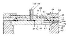
유전체창(12) 상에는, 처리 용기(11) 내의 플라즈마 가스를 여기하는 평면 형상의 마이크로파 안테나(18)가 놓여진다. 마이크로파 안테나(18)는, 동축 모드에서 마이크로파를 상하 방향으로 전반하는 동축 도파관(19)과, 동축 도파관(19)의 동축 도파로(20)를 통과한 마이크로파를 방사 방향으로 전반하는 디스크 형상의 유전체판(22)과, 마이크로파를 투과시키는 슬롯을 갖는 슬롯판(23)과, 유전체판(22)의 상면에 놓여져 유전체판(22)을 냉각하는 냉각판(24)을 포함한다.On the
마이크로파를 급전하는 급전 수단으로서의 동축 도파관(19)은, 수직 방향으로 신장하는 내도체(19a)와, 내도체(19a)를 둘러싸는 통 형상의 외도체(19b)로 이루어진다. 내도체(19a)와 외도체(19b)와의 사이에 단면 환상의 동축 도파로(20)가 형성된다. 동축 도파관(19)의 상단부는 수평 방향으로 신장하는 직사각형 도파관(21)(도 1 참조)에 접속된다. 직사각형 도파관(21)과 동축 도파관(19)의 접속부에는 원추형의 모드 변환기(25)(도 1 참조)가 설치된다. 직사각형 도파관(21)은 정합기를 통하여 마그네트론 등의 마이크로파 발생 장치에 접속되어 있다. 마이크로파 발생 장치는, 예를 들면 주파수 2.45㎓, 8.35㎓, 1.98㎓, 915㎒ 등의 마이크로파를 발생한다. 직사각형 도파관(21)을 전반하는 마이크로파는 모드 변환기(25)에 의해 동축 모드로 변환되어, 동축 도파로(20)(도 3 참조)를 상하 방향으로 전반한다. 정합기는, 마이크로파 발생 장치로부터 발생하는 마이크로파를 직사각형 도파관(21) 및 동축 도파로(20)를 통하여 유전체판(22)으로 전반시킨다.The
유전체판(22)은, Al2O3, 석영 등의 유전체로 이루어진다. 마이크로파는, 전계와 자계가 매우 빠르게 변화하면서 전반하는 전자파이다. 유전체판(22)의 하면에는 금속으로 이루어지는 슬롯판(23)이 설치되고, 유전체판(22)의 상면에는 금속으로 이루어지는 냉각판(24)이 설치된다. 금속면에 닿은 마이크로파는, 금속 내에는 거의 진입하지 않고, 극히 표면(표피 깊이)에 전류를 흘려, 대부분이 반사된다. 이 때문에, 동축 도파로(20)로부터 유전체판(22)에 조사된 마이크로파는, 슬롯판(23) 및 냉각판(24)에 의해 반사되면서 유전체판(22)을 방사 방향으로 전반한다. 또한, 동축 도파로(20)로부터 유전체판(22)으로 들어갈 때, 마이크로파가 전반하는 매질이 공기로부터 유전체로 변화하기 때문에, 마이크로파의 파장이 압축된다. 유전체판(22)의 두께는, TE 모드에서 마이크로파가 전반하도록, 즉 전계가 두께 방향으로만 발생할 수 있도록 결정된다. 유전체판(22)의 두께가 유전체판(22) 내에 있어서의 마이크로파의 파장의 1/4 이하이면 문제없다. 단, 너무 얇으면 강도의 문제가 있고, 또한 너무 두꺼우면 휘기 어려워진다. 이 때문에 본 실시 형태에 있어서, 유전체판(22)의 재질에 알루미나를 사용한 경우, 3∼6㎜ 정도가 최적인 두께가 된다.The
구리판 등으로 이루어지는 슬롯판(23)에는, 마이크로파를 투과시키는 다수의 슬롯(23a)이 뚫린다. 유전체판(22) 내에서 공진한 마이크로파는, 슬롯판(23)의 다수의 슬롯(23a)을 투과하여, 처리 용기(11) 내로 방사된다.In the
도 3에 나타내는 바와 같이, 마이크로파 안테나(18)의 유전체판(22) 상에는, 냉각판(24)이 놓여진다. 냉각판(24)에는 냉각수 유로(24a)가 형성된다. 냉각수 유로(24a)에 냉각수를 흘림으로써, 유전체판(22)을 냉각할 수 있다. 열전도성을 향상시키기 위해, 냉각판(24)과 유전체판(22)과의 사이에는, 완충 시트가 끼워져도 좋다.As shown in FIG. 3, the cooling
마이크로파 안테나(18)는, 유전체창 고정부(14)에 부착되는 안테나 고정부(26)에 의해 유전체창(12)에 고정된다. 안테나 고정부(26)는 처리 용기(11)와 동일하게 Al 또는 Al을 함유하는 스테인리스강으로 이루어진다. 냉각판(24)과 안테나 고정부(26)와의 사이에는, 전자 차폐(遮蔽) 탄력체(27)가 설치된다. 슬롯판(23)의 슬롯(23a)을 투과하는 마이크로파는, 일부가 슬롯판(23)과 유전체창(12)과의 사이의 작은 극간으로부터 외측으로 새어 나간다. 그 뿐만 아니라, 유전체창(12)을 외주 방향으로 전반한 마이크로파는 유전체창 고정부(14)와 냉각판(24)과의 사이의 극간으로부터 외측으로 새어 나간다. 전자 차폐 탄력체(27)는 새어 나간 마이크로파를 실드한다.The
동축 도파관(19)의 내도체(19a)와 외도체(19b)(정확하게 말하면 외도체(19b)를 구성하는 냉각판(24))와의 사이에는, 환상 유전체(28)가 끼워진다. 이 환상 유전체(28)는 유전체판(22)에 일체로 결합된다. 그리고, 내도체(19a)와 환상 유전체(28)와의 사이가 내측 시일 부재로서의 시일 링(29)에 의해 시일되고, 외도체(19b)와 환상 유전체(28)와의 사이가 외측 시일 부재로서의 시일 링(30)에 의해 시일된다.An
유전체창(12), 유전체판(22) 및 냉각판(24)의 외주와, 유전체창 고정부(14) 및 안테나 고정부(26)의 내주와의 사이에 부압로(35)가 형성된다. 냉각판(24)과 안테나 고정부(26)와의 사이는 시일 링(31)에 의해 시일되고, 안테나 고정부(26)와 유전체창 고정부(14)와의 사이는 시일 링(32)에 의해 시일된다. 유전체창 고정부(14)와 처리 용기(11)와의 사이는 시일 링(33)에 의해 시일된다. 부압로(35)에는, 공기를 흡인하는 흡인구(34)가 뚫린다. 흡인구(34)에는, 부압로(35)의 압력을 조정하는 압력 조정기가 접속된다. 압력 조정기에는 진공 펌프가 접속된다. 부압로(35)의 압력을 조정함으로써, 유전체창(12)과 유전체판(22)과의 밀착 정도 및, 유전체판(22)과 냉각판(24)과의 밀착 정도를 조정할 수 있고, 이 때문에 유전체창(12) 및 유전체판(22)의 온도 제어를 행하는 것이 가능해진다.A
동축 도파관(19)이 시일되어 있기 때문에, 흡인구(34)로부터 공기를 흡인하면, 유전체판(22)과 유전체창(12)과의 사이 및, 유전체판(22)과 냉각판(24)과의 사이가 부압으로 된다. 부압의 범위는 1∼600Torr(1.3332×10²∼7.9993×10⁴㎩), 바람직하게는 200∼400Torr(2.6664×10⁴∼5.3328×10⁴㎩)로 설정된다. 압력이 낮으면 낮을수록, 유전체판(22) 및 냉각판(24)을 유전체창(12)에 밀어붙이는 힘을 작용시킬 수 있다. 이 때문에, 부압의 범위는 600Torr(7.9993×10⁴㎩) 이하로 설정된다. 유전체판(22) 및 냉각판(24)을 유전체창(12)에 밀어붙이는 힘을 크게 하기 위해서는, 400Torr(5.3328×10⁴㎩) 이하인 것이 바람직하다. 유전체창(12)은 처리 용기(11) 내의 진공이나 열팽창에 의해, 0.1㎜ 정도 휘는 경우도 있다. 유전체판(22)과 유전체창(12)과의 사이 및, 유전체판(22)과 냉각판(24)과의 사이를 600Torr(7.9993×10⁴㎩) 이하의 부압으로 함으로써, 유전체창(12)의 휨에 맞추어 유전체판(22) 및 냉각판(24)을 휘게 할 수 있다.Since the
부압의 범위를 1Torr(1.3332×10²㎩) 이상으로 한 것은, 1Torr(1.3332×10²) 미만이면, 가스의 분자의 수가 줄어, 열전달을 나쁘게 하기 때문이다. 열을 전달하는 것은 분자이기 때문에 진공 상태로부터 기체의 압력이 높아지면 높아질수록, 기체의 분자의 수가 증가하여, 열전달률이 향상된다. 그러나, 어느 압력을 초과하면, 열전달률이 압력에 의존하지 않게 된다. 그 압력이 1Torr(1.3332×10²㎩) 정도이다. 단, 강한 마이크로파가 전반하는 공간을 부압으로 하면, 이상(異常) 방전(바람직하지 않은 방전)이 일어나기 쉬워진다. 이상 방전을 방지하기 위해 200Torr(2.6664×10⁴㎩) 이상이 바람직하다.Reason why the range of the negative pressure more than1Torr (1.3332 × 10 2 ㎩) , is less than 1Torr (1.3332 × 10²), reduce the number of gas molecules, due to bad heat transfer. Since the heat transfer is a molecule, the higher the pressure of the gas from the vacuum state, the more the number of molecules of the gas increases, and the heat transfer rate is improved. However, if any pressure is exceeded, the heat transfer rate will not depend on the pressure. The pressure is about 1 Torr (1.3332 × 10² kPa). However, if the space where strong microwaves propagate is made negative pressure, abnormal discharge (desirable discharge) is likely to occur. In order to prevent abnormal discharge, 200 Torr (2.6664 x 10⁴ kPa) or more is preferable.
도 4는, 본 발명의 제2 실시 형태의 마이크로파 플라즈마 처리 장치를 나타낸다. 또한, 제1 실시 형태의 마이크로파 플라즈마 처리 장치와 동일한 구성에는 동일한 부호를 붙여 그 설명을 생략한다. 이 실시 형태에 있어서는, 유전체판(22)의 상면, 하면 및 외주면에는, 도전막(41)이 형성된다. 그리고, 유전체창(12)과 유전체판(22)과의 사이에는, 제1 시일 부재로서 O링 등으로 이루어지는 시일 링(42)이 설치된다. 유전체판(22)과 냉각판(24)과의 사이에는, 제2 시일 부재로서 O링 등으로 이루어지는 시일 링(43)이 설치된다. 유전체판(22)의 상면 및 하면에 도전막이 형성되어 있기 때문에, 유전체판(22)과 도전막(41)과의 사이를 시일할 필요는 없다.4 shows a microwave plasma processing apparatus of a second embodiment of the present invention. In addition, the same code | symbol is attached | subjected to the structure same as the microwave plasma processing apparatus of 1st Embodiment, and the description is abbreviate | omitted. In this embodiment, the
도 5는 도전막(41)이 형성된 유전체판(22)의 상세도를 나타낸다. 유전체판(22)의 상면, 하면 및 외주면에는, 금속의 층으로 이루어지는 도전막(41)이 도금된다. 유전체판(22)의 중심부에는, 동축 도파관(19)의 내도체(19a)에 접속되는 슬롯 중심 콘택트 플랜지(40)(도 4 참조)가 관통하는 구멍(22a)이 뚫린다. 구멍(22a)의 주위(유전체판(22)의 상면 및 하면의 일부 및 내주면)에는, 도전막(41)이 성막되어 있지 않은 비성막 에어리어(22b)가 형성된다.5 shows a detailed view of the
유전체판(22)의 하면측의 도전막(41)에는, 마이크로파를 투과시키는 다수의 슬롯(41a)이 형성된다. 인접하는 한 쌍의 슬롯(41a)은, 직교하도록 T자 형상으로 배열된다. 다수의 슬롯(41a)은 디스크 형상의 도전막(41)에 동심원 형상으로 배치된다. 슬롯(41a)의 길이나 배열은, 슬롯(41a)으로부터 처리 용기(11)로 강한 전계가 방사되도록, 유전체판(22)에 의해 압축된 마이크로파의 파장에 따라서 적절히 결정된다. 슬롯(41a)의 형상은 직선 형상 외에 원호 형상이라도 좋고, 슬롯(41a)의 배열은 동심원 형상 외에 나선 형상이나 방사상이라도 좋다.A plurality of
도전막(41)은 유전체판(22)에 이하의 공정을 거쳐 성막된다. 유전체판(22)을 제작한 후, 슬롯(41a)에 대응하는 비성막 에어리어를 마스킹하고, 그 후, 유전체판(22)에 금속층을 도금하고, 그 후 마스킹을 제거한다. 또는, 유전체판(22)을 제작한 후, 유전체판(22)에 금속층을 도금하고, 그 후 슬롯(41a)에 대응하는 부분을 에칭한다.The
도 4에 나타내는 바와 같이, 유전체판(22)의 하면의 도전막(41)은, 슬롯 중심 콘택트 플랜지(40)를 통하여 내도체(19a)에 전기적으로 접속된다. 유전체판(22)의 상면의 도전막(41)은, 냉각판(24)을 통하여 동축 도파관(19)의 외도체(19b)에 전기적으로 접속된다. 유전체판(22)의 하면의 도전막(41)과 동축 도파관(19)의 내도체(19a)를 전기적으로 접속할 필요가 있는 점에서, 원주(圓柱) 형상의 슬롯 중심 콘택트 플랜지(40)와 판 형상의 슬롯 중심 콘택트판(44)이 설치된다. 슬롯 중심 콘택트 플랜지(40)와 슬롯 중심 콘택트판(44)은, 접착, 나사 등에 의해 결합된다. 슬롯 중심 콘택트 플랜지(40)는, 내도체(19a)에 나사 등에 의해 결합된다. O링 등으로 이루어지는 콘택트 보강 탄성체(45)는, 슬롯 중심 콘택트판(44)과 도전막(41)과의 전기적 접촉을 보강하고, 또한 유전체판(22)의 상면측의 도전막(41)과 냉각판(24)과의 전기적 접촉을 보강한다. 슬롯 외주 콘택트 링(46)과 슬롯 외주 콘택트판(47)은 결합된다. 슬롯 외주 콘택트 링(46)은 냉각판(24)에 볼트 등으로 결합된다. O링 등으로 이루어지는 콘택트 보강 탄성체(48)는, 슬롯 외주 콘택트판(47)과 유전체판(22)의 하면측의 도전막(41)과의 전기적 접촉을 보강한다.As shown in FIG. 4, the
도 6은, 본 발명의 제3 실시 형태의 마이크로파 플라즈마 처리 장치를 나타낸다. 이 실시 형태의 마이크로파 플라즈마 처리 장치의 구성은, 제2 실시 형태의 마이크로파 플라즈마 처리와 거의 동일하지만, 시일 개소가 변경되어 있다. 즉, 유전체창 고정부(14)와 유전체창(12)과의 사이 및, 유전체창 고정부(14)와 냉각판(24)과의 사이에 시일 링(51, 52)을 배치하고 있다. 부압로(53)는 유전체판(22) 및 냉각판(24)의 외주와 유전체창 고정부(14)의 내주와의 사이에 형성된다. 공기를 흡인하는 흡인구(54)는 유전체창 고정부(14)에 형성된다. 이와 같이 시일 링을 배치해도, 유전체창(12)과 유전체판(22)과의 사이 및, 유전체판(22)과 냉각판(24)과의 사이를 부압으로 할 수 있다.6 shows a microwave plasma processing apparatus of a third embodiment of the present invention. The configuration of the microwave plasma processing apparatus of this embodiment is almost the same as that of the microwave plasma processing of the second embodiment, but the seal point is changed. That is, the seal rings 51 and 52 are arrange | positioned between the dielectric
도 7은, 본 발명의 제4 실시 형태의 마이크로파 플라즈마 처리 장치를 나타낸다. 이 실시 형태의 플라즈마 처리 장치에 있어서는, 냉각판(24)과 유전체판(22)과의 밀착성을 향상시키기 위해, 냉각판(24)과 유전체판(22)과의 사이가 부압으로 된다. 유전체판(22)의 상면 및 하면에는 도전막(41)이 형성된다. 냉각판(24)과 유전체판(22)의 내주측과의 사이에는, 내측 시일 부재로서 O링 등으로 이루어지는 시일 링(56)이 설치된다. 냉각판(24)과 유전체판(22)의 외주측과의 사이에는, 외측 시일 부재로서 O링 등으로 이루어지는 시일 링(57)이 설치된다. 냉각판(24)의, 내측의 시일 링(56)과 외측의 시일 링(57)과의 사이에는 공기를 흡인하는 흡인구(58)가 형성된다. 유전체판(22)의 상면에 마이크로파를 반사하는 도전막(41)을 형성함으로써, 냉각판(24)에 흡인구(58)나 홈을 형성해도 마이크로파의 전반 특성에 영향을 주는 일은 없다. 이 때문에, 유전체판(22)에 도전막(41)을 형성시키는 것이 바람직하지만, 반드시 형성시키지 않아도 좋다.7 shows a microwave plasma processing apparatus of a fourth embodiment of the present invention. In the plasma processing apparatus of this embodiment, the negative pressure is between the cooling
냉각판(24)과 유전체판(22)과의 사이를 부압으로 함으로써, 냉각판(24)과 유전체판(22)과의 밀착성을 향상시킬 수 있다. 또한, 유전체창(12)으로부터 도전막(41)에 인장력을 작용시킬 수 있어, 유전체창(12)이 휘는 것을 방지할 수 있다.By making negative pressure between the cooling
도 8은, 본 발명의 제5 실시 형태의 마이크로파 플라즈마 처리 장치를 나타낸다. 이 실시 형태에서는, 도 4에 나타나는 제2 실시 형태의 마이크로파 플라즈마 처리 장치의 시일 링의 위치(43)를 바꾸고 있다. 즉, 유전체판(22)과 냉각판(24)과의 사이를 시일하는 시일 링(43)을, 유전체판(22) 및 냉각판(24)의 외주측에 배치하고 있다. 시일 링(43)을 유전체판(22) 및 냉각판(24)의 외주측에 배치함으로써, 유전체판(22)과 유전체창(12)과의 사이만을 부압으로 하는 것이 가능해진다. 나머지의 구성, 예를 들면 유전체판(22)의 상면 및 하면에 도전막(41)이 형성되는 점, 유전체판(22)과 유전체창(12)과의 사이에 시일 링(42)이 배치되는 점 등은, 도 4에 나타나는 제2 실시 형태의 마이크로파 플라즈마 처리 장치와 동일하기 때문에, 동일한 부호를 붙여 그 설명을 생략한다. 유전체판(22)과 유전체창(12)과의 사이를 1∼600Torr(1.3332×10²∼7.9993×10⁴㎩)의 범위의 부압으로 함으로써, 유전체판(22)을 유전체창(12)에 밀어붙여, 유전체창(12)의 휨에 맞추어 유전체판(22)을 밀착시킬 수 있다.8 shows a microwave plasma processing apparatus of a fifth embodiment of the present invention. In this embodiment, the
도 9는, 본 발명의 제6 실시 형태의 마이크로파 플라즈마 처리 장치를 나타낸다. 이 실시 형태에서도, 제5 실시 형태의 마이크로파 플라즈마 처리 장치와 동일하게, 유전체판(22)과 유전체창(12)과의 사이만을 부압으로 하기 위한 궁리가 이루어지고 있다. 유전체판(22)의 상면 및 하면에는 도전막(41)이 형성된다. 유전체판(22)의 내주측과 유전체창(12)의 내주측과의 사이에는, 내측 시일 부재로서 O링 등으로 이루어지는 시일 링(61)이 설치된다. 유전체판(22)의 외주측과 유전체창(12)의 외주측과의 사이에는, 외측 시일 부재로서 O링 등으로 이루어지는 시일 링(62)이 설치된다. 유전체창(12)의, 내측의 시일 링(61)과 외측의 시일 링(62)과의 사이에는 공기를 흡인하는 흡인구(63)가 형성된다. 흡인구(63)에 연결되는 흡인 경로(64)는, 흡인구(63)로부터 연직 하방으로 신장된 후, 90도 구부러져 수평 방향으로 신장되어, 유전체창(12)의 외주면에 노출된다.9 shows a microwave plasma processing apparatus of a sixth embodiment of the present invention. Also in this embodiment, similarly to the microwave plasma processing apparatus of the fifth embodiment, the inventors have devised a negative pressure only between the
유전체창(12)의 외주면과 처리 용기(11)의 유전체창 수용틀(65)의 내주면과의 사이에 부압로(66)가 형성된다. 유전체창 고정부(14)와 처리 용기(11)와의 사이는 시일 링(67)에 의해 시일되고, 안테나 고정부(26)와 유전체창(12)과의 사이는 시일 링(68)에 의해 시일된다. 유전체창(12)과 처리 용기(11)의 유전체창 수용틀(65)과의 사이는 시일 링(69)에 의해 시일된다. 처리 용기(11)에는, 부압로(66)에 연결되는 흡인 경로(70)가 형성된다. 흡인 경로(70)로부터 공기를 흡인함으로써, 유전체판(22)과 유전체창(12)과의 사이를 부압으로 할 수 있다. 유전체판(22)과 유전체창(12)과의 사이를 1∼600Torr(1.3332×10²∼7.9993×10⁴㎩)의 범위의 부압으로 함으로써, 유전체판(22)을 유전체창(12)에 밀어붙임으로써, 유전체창(12)의 휨에 맞추어 유전체판(22)을 밀착시킬 수 있다.A
또한, 본 발명은 상기 실시 형태로 한정되는 일 없이, 본 발명의 요지를 변경하지 않는 범위에서 여러 가지로 변경할 수 있다. 예를 들면 도 10에 나타내는 바와 같이, 본 발명의 안테나는, 동축 도파로와 같이 중심으로부터 밖을 향하여 마이크로파를 넓히는 구조가 아니더라도, 급전 수단으로서의 직사각형 도파관(51)에 의해 수평 방향으로 마이크로파를 도입하는 구조여도 좋다.In addition, this invention can be variously changed in the range which does not change the summary of this invention, without being limited to the said embodiment. For example, as shown in FIG. 10, the antenna of the present invention has a structure in which microwaves are introduced in the horizontal direction by a
유전체판과 유전체창과의 사이, 및/또는 유전체판과 냉각판과의 사이를 배기하기 쉽도록, 유전체판의 유전체창 및/또는 냉각판측에, 배기용의 홈(깊이 20㎛ 정도, 폭 3㎜ 정도)을 형성하는 것이 바람직하다.In the dielectric window and / or the cooling plate side of the dielectric plate to facilitate the evacuation between the dielectric plate and the dielectric window and / or between the dielectric plate and the cooling plate, grooves for exhausting (about 20 µm deep and 3 mm wide) Degree).
유전체판과 유전체창과의 사이, 및/또는 유전체판과 냉각판과의 사이를 부압으로 할 수 있으면, 시일 링의 배치 개수, 위치는 상기 실시 형태로 한정되는 일은 없고, 적절히 변경할 수 있다.If the negative pressure can be made between the dielectric plate and the dielectric window and / or between the dielectric plate and the cooling plate, the number and positions of the seal rings are not limited to the above embodiments, and can be changed as appropriate.
또한, 유전체와 유전체창과의 사이, 및/또는 유전체판과 냉각판과의 사이에는, 열전도성이 좋은 테플론(등록 상표) 시트, 카본 시트 등의 완충 시트를 끼워도 좋다.Further, a buffer sheet such as a Teflon (registered trademark) sheet or a carbon sheet having good thermal conductivity may be interposed between the dielectric and the dielectric window and / or between the dielectric plate and the cooling plate.
또한, 공기를 흡인한 부압로에 He 가스 등의 전열성 가스를 밀봉입해도 좋다. 전열성 가스를 밀봉입했을 때도 압력은 대기압보다도 낮은 부압으로 조정된다.Moreover, you may seal-in an electrothermal gas, such as He gas, in the negative pressure furnace which attracted air. Even when the heat-transfer gas is sealed in, the pressure is adjusted to a negative pressure lower than atmospheric pressure.
또한, 유전체창에 처리 용기 내에 플라즈마 가스를 공급하는 플라즈마 가스 공급 경로를 형성하고, 유전체창과 피처리 기판과의 사이에 처리 가스를 공급하는 중단(中段) 샤워 헤드를 설치해도 좋다.In addition, a plasma gas supply path for supplying plasma gas into the processing container may be formed in the dielectric window, and an intermediate shower head may be provided for supplying the processing gas between the dielectric window and the substrate to be processed.
본 명세서는, 2009년 3월 23일 출원된 일본특허출원 2009-070943에 기초한다. 이 내용은 모두 여기에 포함해 둔다.This specification is based on the JP Patent application 2009-070943 of the March 23, 2009 application. All of this is included here.
11 : 처리 용기
12 : 유전체창
14 : 유전체창 고정부
15 : 가스 공급부
16 : 보지대
18 : 마이크로파 안테나
19 : 동축 도파관
19a : 내도체
19b : 외도체
20 : 동축 도파로
22 : 유전체판
23 : 슬롯판
23a : 슬롯
24 : 냉각판
28 : 환상 유전체
29 : 시일 링(내측 시일 부재)
30 : 시일 링(외측 시일 부재)
34 : 흡인구
35 : 부압로
41 : 도전막(슬롯판)
41a : 슬롯
42 : 시일 링(제1 시일 부재)
43 : 시일 링(제2 시일 부재)
53 : 부압로
54 : 흡인구
56 : 시일 링(내측 시일 부재)
57 : 시일 링(외측 시일 부재)
58 : 흡인구11: Processing vessel
12: dielectric window
14: dielectric window fixing part
15 gas supply unit
16: music stand
18: microwave antenna
19: coaxial waveguide
19a: inner conductor
19b: outer conductor
20: coaxial waveguide
22: dielectric plate
23: slot plate
23a: slot
24: cold plate
28: annular dielectric
29: seal ring (inner seal member)
30: seal ring (outer seal member)
34: suction port
35: negative pressure furnace
41: conductive film (slot plate)
41a: slot
42: seal ring (first seal member)
43: seal ring (second seal member)
53: negative pressure furnace
54: suction port
56: seal ring (inner seal member)
57: seal ring (outer seal member)
58: suction port
Claims (20)
Translated fromKorean상기 마이크로파 안테나는, 수평 방향으로 마이크로파를 전파함과 함께 마이크로파의 파장을 압축하는 유전체판과, 상기 유전체판과 상기 유전체창과의 사이에 설치되어, 마이크로파를 투과시키는 슬롯을 갖는 슬롯판과, 상기 유전체판의 상면에 놓여져 상기 유전체판을 냉각하는 냉각판을 포함하고,
상기 유전체판과 상기 냉각판과의 사이가 대기압보다도 압력이 낮은 부압으로 되는 마이크로파 플라즈마 처리 장치.A processing vessel in which the ceiling is defined by a dielectric window, a gas exhaust system for depressurizing the processing container, a plasma gas supply unit for supplying plasma gas to the processing container, and a dielectric window of the processing container, In the microwave plasma processing apparatus provided with the microwave antenna which excites plasma gas,
The microwave antenna includes a dielectric plate that propagates microwaves in a horizontal direction and compresses wavelengths of microwaves, a slot plate provided between the dielectric plate and the dielectric window and having a slot for transmitting microwaves, and the dielectric material. A cooling plate placed on an upper surface of the plate to cool the dielectric plate,
A microwave plasma processing apparatus in which a pressure between the dielectric plate and the cooling plate becomes a negative pressure lower than atmospheric pressure.
상기 냉각판과 상기 유전체판의 내주측과의 사이가 환상의 내측 시일 부재로 시일됨과 함께, 상기 냉각판과 상기 유전체판의 외주측과의 사이가 환상의 외측 시일 부재로 시일되고,
상기 냉각판의, 상기 내측 시일 부재와 외측 시일 부재와의 사이에는, 가스를 흡인하는 흡인구가 형성되는 것을 특징으로 하는 마이크로파 플라즈마 처리 장치.The method of claim 10,
Between the cooling plate and the inner circumferential side of the dielectric plate is sealed with an annular inner seal member, and between the cooling plate and the outer circumferential side of the dielectric plate is sealed with an annular outer seal member,
A suction port for sucking a gas is formed between the inner seal member and the outer seal member of the cooling plate.
상기 마이크로파 안테나는, 수평 방향으로 마이크로파를 전파함과 함께 마이크로파의 파장을 압축하는 유전체판과, 상기 유전체판과 상기 유전체창과의 사이에 설치되어, 마이크로파를 투과시키는 슬롯을 갖는 슬롯판과, 상기 유전체판의 상면에 놓여져 상기 유전체판을 냉각하는 냉각판을 포함하고,
상기 유전체창과 상기 유전체판과의 사이 및, 상기 유전체판과 상기 냉각판과의 사이가 대기압보다도 압력이 낮은 부압으로 되는 마이크로파 플라즈마 처리 장치.A processing vessel in which the ceiling is defined by a dielectric window, a gas exhaust system for depressurizing the processing container, a plasma gas supply unit for supplying plasma gas to the processing container, and a dielectric window of the processing container, In the microwave plasma processing apparatus provided with the microwave antenna which excites plasma gas,
The microwave antenna includes a dielectric plate that propagates microwaves in a horizontal direction and compresses wavelengths of microwaves, a slot plate provided between the dielectric plate and the dielectric window and having a slot for transmitting microwaves, and the dielectric material. A cooling plate placed on an upper surface of the plate to cool the dielectric plate,
A microwave plasma processing apparatus comprising a negative pressure having a pressure lower than atmospheric pressure between the dielectric window and the dielectric plate and between the dielectric plate and the cooling plate.
상기 부압은, 1∼600Torr(1.3332×10²∼7.9993×10⁴㎩)의 범위인 마이크로파 플라즈마 처리 장치.13. The method according to claim 10 or 12,
The said negative pressure is the microwave plasma processing apparatus of 1-600 Torr (1.3332 * 10 <2> -7.9993 * 10 <4> Pa).
상기 부압의 범위가 200∼400Torr(2.6664×10⁴∼5.3329×10⁴㎩)인 것을 특징으로 하는 마이크로파 플라즈마 처리 장치.The method of claim 13,
The negative pressure ranges from 200 to 400 Torr (2.6664 x 10⁴ to 5.3329 x 10⁴ Pa).
상기 슬롯판은, 상기 유전체판의 하면측에 형성된 도전막으로 이루어지는 것을 특징으로 하는 마이크로파 플라즈마 처리 장치.The method of claim 10,
The slot plate is made of a conductive film formed on the lower surface side of the dielectric plate.
상기 유전체판의 상면에, 마이크로파를 반사하는 도전막이 형성되는 것을 특징으로 하는 마이크로파 플라즈마 처리 장치.16. The method of claim 15,
A microwave plasma processing apparatus, wherein a conductive film for reflecting microwaves is formed on an upper surface of the dielectric plate.
상기 처리 용기의 상부에는 동축도파관이 배치되고,
상기 동축도파관은, 중앙에 배치되는 내(內)도체와, 상기 내도체의 외주측에 배치되는 외(外)도체를 갖고, 상기 내도체와 상기 외도체의 사이에는 동축도파로가 형성되고,
상기 동축 도파로에는, 환상(環狀) 유전체가 끼워지고,
상기 내도체와 상기 환상 유전체와의 사이가 내측 시일 부재로 시일됨과 함께, 상기 외도체와 상기 환상 유전체와의 사이가 외측 시일 부재로 시일되는 것을 특징으로 하는 마이크로파 플라즈마 처리 장치.13. The method according to claim 10 or 12,
Coaxial waveguide is disposed on the upper portion of the processing container,
The coaxial waveguide has an inner conductor disposed in the center and an outer conductor disposed on an outer circumferential side of the inner conductor, and a coaxial waveguide is formed between the inner conductor and the outer conductor,
An annular dielectric material is inserted into the coaxial waveguide,
And the space between the inner conductor and the annular dielectric is sealed with an inner seal member, and the space between the outer conductor and the annular dielectric is sealed with an outer seal member.
상기 유전체판의 하면에는, 상기 슬롯판으로서의 도전막이 형성되고,
상기 유전체판의 상면에는, 마이크로파를 반사하는 도전막이 형성되고,
상기 유전체판의 하면측의 도전막과 상기 유전체창과의 사이가 환상의 제1 시일 부재로 시일됨과 함께, 상기 유전체판의 상면측의 도전막과 상기 냉각판과의 사이가 환상의 제2 시일 부재로 시일되는 것을 특징으로 하는 마이크로파 플라즈마 처리 장치.13. The method according to claim 10 or 12,
On the lower surface of the dielectric plate, a conductive film as the slot plate is formed,
On the upper surface of the dielectric plate, a conductive film for reflecting microwaves is formed,
The annular first seal member is sealed between the conductive film on the lower surface side of the dielectric plate and the dielectric window, and the annular second seal member is formed between the conductive film on the upper surface side of the dielectric plate and the cooling plate. Microwave plasma processing apparatus characterized in that the seal.
상기 처리 용기에는, 상기 유전체창을 상기 처리 용기에 고정하기 위한 유전체창 고정 부재 및, 상기 마이크로파 안테나를 상기 유전체창에 고정하기 위한 안테나 고정 수단이 구비되고,
상기 유전체창, 상기 유전체판 및 상기 냉각판의 외주와, 상기 유전체창 고정 부재 및 상기 안테나 고정 수단의 내주와의 사이에 부압로가 형성되고,
상기 부압로에 가스를 흡인하는 흡인구가 형성되는 것을 특징으로 하는 마이크로파 플라즈마 처리 장치.13. The method according to claim 10 or 12,
The processing container includes a dielectric window fixing member for fixing the dielectric window to the processing container, and antenna fixing means for fixing the microwave antenna to the dielectric window,
A negative pressure path is formed between the outer circumference of the dielectric window, the dielectric plate and the cooling plate, and the inner circumference of the dielectric window fixing member and the antenna fixing means.
And a suction port for sucking a gas in the negative pressure path.
상기 유전체창과 상기 유전체판과의 사이 및, 상기 유전체판과 상기 냉각판과의 사이의 압력을 조정함으로써, 상기 유전체창 및 상기 유전체판의 온도 제어를 행하는 것을 특징으로 하는 마이크로파 플라즈마 처리 장치.
13. The method according to claim 10 or 12,
Temperature control of the dielectric window and the dielectric plate is performed by adjusting the pressure between the dielectric window and the dielectric plate and between the dielectric plate and the cooling plate.
Applications Claiming Priority (3)
| Application Number | Priority Date | Filing Date | Title |
|---|---|---|---|
| JP2009070943AJP5461040B2 (en) | 2009-03-23 | 2009-03-23 | Microwave plasma processing equipment |
| JPJP-P-2009-070943 | 2009-03-23 | ||
| PCT/JP2010/054100WO2010110080A1 (en) | 2009-03-23 | 2010-03-11 | Microwave plasma processing apparatus |
Publications (2)
| Publication Number | Publication Date |
|---|---|
| KR20110128888A KR20110128888A (en) | 2011-11-30 |
| KR101256850B1true KR101256850B1 (en) | 2013-04-22 |
Family
ID=42780773
Family Applications (1)
| Application Number | Title | Priority Date | Filing Date |
|---|---|---|---|
| KR1020117022121AExpired - Fee RelatedKR101256850B1 (en) | 2009-03-23 | 2010-03-11 | Microwave plasma processing apparatus |
Country Status (5)
| Country | Link |
|---|---|
| JP (1) | JP5461040B2 (en) |
| KR (1) | KR101256850B1 (en) |
| CN (1) | CN102362557A (en) |
| TW (1) | TW201116168A (en) |
| WO (1) | WO2010110080A1 (en) |
Families Citing this family (8)
| Publication number | Priority date | Publication date | Assignee | Title |
|---|---|---|---|---|
| JP4980475B1 (en)* | 2011-03-31 | 2012-07-18 | 三井造船株式会社 | Induction heating device |
| KR101299702B1 (en)* | 2011-05-31 | 2013-08-28 | 세메스 주식회사 | Substrate treating apparatus |
| JP2014154684A (en)* | 2013-02-07 | 2014-08-25 | Tokyo Electron Ltd | Inductively coupled plasma processing apparatus |
| JP6850636B2 (en)* | 2017-03-03 | 2021-03-31 | 東京エレクトロン株式会社 | Plasma processing equipment |
| JP7067913B2 (en)* | 2017-12-13 | 2022-05-16 | 東京エレクトロン株式会社 | Plasma processing equipment |
| KR102524258B1 (en)* | 2018-06-18 | 2023-04-21 | 삼성전자주식회사 | Temperature control unit, temperature measurement unit and plasma processing apparatus including the same |
| CN111640642B (en)* | 2019-03-01 | 2023-08-18 | 北京北方华创微电子装备有限公司 | Antenna mechanism and surface wave plasma processing equipment |
| KR102567508B1 (en) | 2020-12-21 | 2023-08-16 | 세메스 주식회사 | Apparatus for porcessing a substrate and method for processing a substrate |
Citations (2)
| Publication number | Priority date | Publication date | Assignee | Title |
|---|---|---|---|---|
| JP2002355550A (en)* | 2001-03-28 | 2002-12-10 | Tadahiro Omi | Plasma treatment apparatus, plasma treatment method and slow-wave plate |
| JP2008243827A (en)* | 2001-03-28 | 2008-10-09 | Tadahiro Omi | Plasma processing method |
Family Cites Families (2)
| Publication number | Priority date | Publication date | Assignee | Title |
|---|---|---|---|---|
| JP2001203098A (en)* | 2000-01-18 | 2001-07-27 | Rohm Co Ltd | Structure of radial line slot antenna in a plasma surface processing apparatus for semiconductor substrate |
| JP2008305736A (en)* | 2007-06-11 | 2008-12-18 | Tokyo Electron Ltd | Plasma processing apparatus, method of using plasma processing apparatus, and method of cleaning plasma processing apparatus |
- 2009
- 2009-03-23JPJP2009070943Apatent/JP5461040B2/ennot_activeExpired - Fee Related
- 2010
- 2010-03-11CNCN201080013280XApatent/CN102362557A/enactivePending
- 2010-03-11KRKR1020117022121Apatent/KR101256850B1/ennot_activeExpired - Fee Related
- 2010-03-11WOPCT/JP2010/054100patent/WO2010110080A1/enactiveApplication Filing
- 2010-03-19TWTW099108139Apatent/TW201116168A/enunknown
Patent Citations (2)
| Publication number | Priority date | Publication date | Assignee | Title |
|---|---|---|---|---|
| JP2002355550A (en)* | 2001-03-28 | 2002-12-10 | Tadahiro Omi | Plasma treatment apparatus, plasma treatment method and slow-wave plate |
| JP2008243827A (en)* | 2001-03-28 | 2008-10-09 | Tadahiro Omi | Plasma processing method |
Also Published As
| Publication number | Publication date |
|---|---|
| CN102362557A (en) | 2012-02-22 |
| TW201116168A (en) | 2011-05-01 |
| WO2010110080A1 (en) | 2010-09-30 |
| JP5461040B2 (en) | 2014-04-02 |
| KR20110128888A (en) | 2011-11-30 |
| JP2010225396A (en) | 2010-10-07 |
Similar Documents
| Publication | Publication Date | Title |
|---|---|---|
| KR101256850B1 (en) | Microwave plasma processing apparatus | |
| JP4694596B2 (en) | Microwave plasma processing apparatus and microwave power feeding method | |
| KR100794806B1 (en) | Plasma processing apparatus and method, and slot antenna | |
| US20080105650A1 (en) | Plasma processing device and plasma processing method | |
| JP5189999B2 (en) | Microwave plasma processing apparatus and microwave power supply method for microwave plasma processing apparatus | |
| JP4593652B2 (en) | Microwave plasma processing equipment | |
| KR101343967B1 (en) | Plasma processing apparatus and method | |
| US7478609B2 (en) | Plasma process apparatus and its processor | |
| JP5297885B2 (en) | Microwave plasma processing equipment | |
| WO2010007863A1 (en) | Microwave plasma processing apparatus and method for producing cooling jacket | |
| US7302910B2 (en) | Plasma apparatus and production method thereof | |
| US7807019B2 (en) | Radial antenna and plasma processing apparatus comprising the same | |
| WO2010086950A1 (en) | Microwave plasma processing apparatus, dielectric board provided with slot board for microwave plasma processing apparatus, and method for manufacturing dielectric board | |
| JP5374853B2 (en) | Plasma processing equipment | |
| KR20090009369A (en) | Plasma reactor with inductively coupled plasma source with heater | |
| WO2010016423A1 (en) | Dielectric window, dielectric window manufacturing method, and plasma treatment apparatus | |
| JP4086450B2 (en) | Microwave antenna and microwave plasma processing apparatus | |
| JP2008182713A (en) | Microwave antenna and microwave plasma processing apparatus | |
| KR20220119357A (en) | plasma processing unit | |
| JP2009146837A (en) | Surface wave exciting plasma treatment device | |
| WO2013124898A1 (en) | Plasma processing device and plasma processing method | |
| JP2013175480A (en) | Plasma processing apparatus and plasma processing method | |
| JP2007059782A (en) | Spacer member and plasma processing device | |
| JP2001118698A (en) | Method and apparatus for generating surface wave excited plasma | |
| JPWO2010016414A1 (en) | Microwave plasma generator and microwave plasma processing apparatus |
Legal Events
| Date | Code | Title | Description |
|---|---|---|---|
| A201 | Request for examination | ||
| P11-X000 | Amendment of application requested | St.27 status event code:A-2-2-P10-P11-nap-X000 | |
| P13-X000 | Application amended | St.27 status event code:A-2-2-P10-P13-nap-X000 | |
| PA0105 | International application | St.27 status event code:A-0-1-A10-A15-nap-PA0105 | |
| PA0201 | Request for examination | St.27 status event code:A-1-2-D10-D11-exm-PA0201 | |
| PG1501 | Laying open of application | St.27 status event code:A-1-1-Q10-Q12-nap-PG1501 | |
| E902 | Notification of reason for refusal | ||
| PE0902 | Notice of grounds for rejection | St.27 status event code:A-1-2-D10-D21-exm-PE0902 | |
| T11-X000 | Administrative time limit extension requested | St.27 status event code:U-3-3-T10-T11-oth-X000 | |
| E13-X000 | Pre-grant limitation requested | St.27 status event code:A-2-3-E10-E13-lim-X000 | |
| P11-X000 | Amendment of application requested | St.27 status event code:A-2-2-P10-P11-nap-X000 | |
| P13-X000 | Application amended | St.27 status event code:A-2-2-P10-P13-nap-X000 | |
| E701 | Decision to grant or registration of patent right | ||
| PE0701 | Decision of registration | St.27 status event code:A-1-2-D10-D22-exm-PE0701 | |
| GRNT | Written decision to grant | ||
| PR0701 | Registration of establishment | St.27 status event code:A-2-4-F10-F11-exm-PR0701 | |
| PR1002 | Payment of registration fee | St.27 status event code:A-2-2-U10-U12-oth-PR1002 Fee payment year number:1 | |
| PG1601 | Publication of registration | St.27 status event code:A-4-4-Q10-Q13-nap-PG1601 | |
| FPAY | Annual fee payment | Payment date:20160318 Year of fee payment:4 | |
| PR1001 | Payment of annual fee | St.27 status event code:A-4-4-U10-U11-oth-PR1001 Fee payment year number:4 | |
| FPAY | Annual fee payment | Payment date:20170322 Year of fee payment:5 | |
| PR1001 | Payment of annual fee | St.27 status event code:A-4-4-U10-U11-oth-PR1001 Fee payment year number:5 | |
| FPAY | Annual fee payment | Payment date:20180329 Year of fee payment:6 | |
| PR1001 | Payment of annual fee | St.27 status event code:A-4-4-U10-U11-oth-PR1001 Fee payment year number:6 | |
| LAPS | Lapse due to unpaid annual fee | ||
| PC1903 | Unpaid annual fee | St.27 status event code:A-4-4-U10-U13-oth-PC1903 Not in force date:20190417 Payment event data comment text:Termination Category : DEFAULT_OF_REGISTRATION_FEE | |
| PC1903 | Unpaid annual fee | St.27 status event code:N-4-6-H10-H13-oth-PC1903 Ip right cessation event data comment text:Termination Category : DEFAULT_OF_REGISTRATION_FEE Not in force date:20190417 |