KR101256709B1 - Multi-layer sheet for use in electro-optic displays - Google Patents
Multi-layer sheet for use in electro-optic displaysDownload PDFInfo
- Publication number
- KR101256709B1 KR101256709B1KR1020097015374AKR20097015374AKR101256709B1KR 101256709 B1KR101256709 B1KR 101256709B1KR 1020097015374 AKR1020097015374 AKR 1020097015374AKR 20097015374 AKR20097015374 AKR 20097015374AKR 101256709 B1KR101256709 B1KR 101256709B1
- Authority
- KR
- South Korea
- Prior art keywords
- layer
- electro
- light
- transmissive
- film
- Prior art date
- Legal status (The legal status is an assumption and is not a legal conclusion. Google has not performed a legal analysis and makes no representation as to the accuracy of the status listed.)
- Active
Links
- 239000010410layerSubstances0.000claimsabstractdescription208
- 230000004888barrier functionEffects0.000claimsabstractdescription74
- 238000000034methodMethods0.000claimsabstractdescription42
- 239000011241protective layerSubstances0.000claimsabstractdescription23
- 230000008569processEffects0.000claimsabstractdescription22
- 229920000642polymerPolymers0.000claimsdescription40
- 239000012790adhesive layerSubstances0.000claimsdescription36
- 230000000873masking effectEffects0.000claimsdescription34
- 238000004519manufacturing processMethods0.000claimsdescription12
- 239000006097ultraviolet radiation absorberSubstances0.000claimsdescription12
- 238000000576coating methodMethods0.000claimsdescription10
- 239000011248coating agentSubstances0.000claimsdescription8
- 238000010030laminatingMethods0.000claimsdescription6
- AMGQUBHHOARCQH-UHFFFAOYSA-Nindium;oxotinChemical compound[In].[Sn]=OAMGQUBHHOARCQH-UHFFFAOYSA-N0.000claimsdescription3
- TWNQGVIAIRXVLR-UHFFFAOYSA-Noxo(oxoalumanyloxy)alumaneChemical compoundO=[Al]O[Al]=OTWNQGVIAIRXVLR-UHFFFAOYSA-N0.000claimsdescription3
- 239000011229interlayerSubstances0.000claimsdescription2
- 238000010348incorporationMethods0.000claims1
- 229920000139polyethylene terephthalatePolymers0.000description34
- 239000005020polyethylene terephthalateSubstances0.000description34
- 239000007787solidSubstances0.000description18
- 239000000463materialSubstances0.000description14
- 239000000758substrateSubstances0.000description9
- 229910052782aluminiumInorganic materials0.000description7
- XAGFODPZIPBFFR-UHFFFAOYSA-NaluminiumChemical compound[Al]XAGFODPZIPBFFR-UHFFFAOYSA-N0.000description7
- 239000000853adhesiveSubstances0.000description6
- 230000001070adhesive effectEffects0.000description6
- 239000000919ceramicSubstances0.000description6
- 238000003475laminationMethods0.000description6
- 239000004973liquid crystal related substanceSubstances0.000description6
- 229910052751metalInorganic materials0.000description6
- 239000002184metalSubstances0.000description6
- 238000000429assemblyMethods0.000description5
- 239000012530fluidSubstances0.000description5
- 239000002245particleSubstances0.000description5
- 230000005855radiationEffects0.000description5
- 239000002775capsuleSubstances0.000description4
- 230000001413cellular effectEffects0.000description4
- 230000008859changeEffects0.000description4
- 239000007788liquidSubstances0.000description4
- 230000003287optical effectEffects0.000description4
- 229920006254polymer filmPolymers0.000description4
- 229920001609Poly(3,4-ethylenedioxythiophene)Polymers0.000description3
- 229920001940conductive polymerPolymers0.000description3
- 239000000382optic materialSubstances0.000description3
- 230000004224protectionEffects0.000description3
- 229920004439Aclar®Polymers0.000description2
- 229920002799BoPETPolymers0.000description2
- OKTJSMMVPCPJKN-UHFFFAOYSA-NCarbonChemical compound[C]OKTJSMMVPCPJKN-UHFFFAOYSA-N0.000description2
- VYPSYNLAJGMNEJ-UHFFFAOYSA-NSilicium dioxideChemical compoundO=[Si]=OVYPSYNLAJGMNEJ-UHFFFAOYSA-N0.000description2
- 230000006750UV protectionEffects0.000description2
- 230000002745absorbentEffects0.000description2
- 239000002250absorbentSubstances0.000description2
- 238000010521absorption reactionMethods0.000description2
- QVGXLLKOCUKJST-UHFFFAOYSA-Natomic oxygenChemical compound[O]QVGXLLKOCUKJST-UHFFFAOYSA-N0.000description2
- 239000002041carbon nanotubeSubstances0.000description2
- 229910021393carbon nanotubeInorganic materials0.000description2
- 229940032122clarisDrugs0.000description2
- 238000009792diffusion processMethods0.000description2
- 230000005684electric fieldEffects0.000description2
- 239000007789gasSubstances0.000description2
- 229920001519homopolymerPolymers0.000description2
- 229910044991metal oxideInorganic materials0.000description2
- 150000004706metal oxidesChemical class0.000description2
- 229910052760oxygenInorganic materials0.000description2
- 239000001301oxygenSubstances0.000description2
- 239000005023polychlorotrifluoroethylene (PCTFE) polymerSubstances0.000description2
- 230000035945sensitivityEffects0.000description2
- HBMJWWWQQXIZIP-UHFFFAOYSA-Nsilicon carbideChemical compound[Si+]#[C-]HBMJWWWQQXIZIP-UHFFFAOYSA-N0.000description2
- 229910010271silicon carbideInorganic materials0.000description2
- 229910052814silicon oxideInorganic materials0.000description2
- 238000004544sputter depositionMethods0.000description2
- IHCDKJZZFOUARO-UHFFFAOYSA-Msulfacetamide sodiumChemical compoundO.[Na+].CC(=O)[N-]S(=O)(=O)C1=CC=C(N)C=C1IHCDKJZZFOUARO-UHFFFAOYSA-M0.000description2
- 229920000134Metallised filmPolymers0.000description1
- 239000005041Mylar™Substances0.000description1
- 239000006096absorbing agentSubstances0.000description1
- 208000033853acromesomelic dysplasia 4Diseases0.000description1
- 230000002411adverseEffects0.000description1
- 230000005540biological transmissionEffects0.000description1
- 230000001427coherent effectEffects0.000description1
- 239000003086colorantSubstances0.000description1
- 239000012612commercial materialSubstances0.000description1
- 230000001010compromised effectEffects0.000description1
- 230000007547defectEffects0.000description1
- 230000032798delaminationEffects0.000description1
- 238000005516engineering processMethods0.000description1
- 239000011521glassSubstances0.000description1
- 238000003384imaging methodMethods0.000description1
- 239000011159matrix materialSubstances0.000description1
- 239000012528membraneSubstances0.000description1
- 150000002739metalsChemical class0.000description1
- 239000003094microcapsuleSubstances0.000description1
- 239000011224oxide ceramicSubstances0.000description1
- 230000000704physical effectEffects0.000description1
- 229920003207poly(ethylene-2,6-naphthalate)Polymers0.000description1
- 229920000515polycarbonatePolymers0.000description1
- 239000004417polycarbonateSubstances0.000description1
- 239000011112polyethylene naphthalateSubstances0.000description1
- 229920005596polymer binderPolymers0.000description1
- 239000002491polymer binding agentSubstances0.000description1
- 230000009467reductionEffects0.000description1
- 230000002829reductive effectEffects0.000description1
- 230000004044responseEffects0.000description1
- 238000005096rolling processMethods0.000description1
- 239000004065semiconductorSubstances0.000description1
- 239000002356single layerSubstances0.000description1
- 238000003860storageMethods0.000description1
- -1tetrabutylammonium hexafluorophosphateChemical compound0.000description1
- 238000009736wettingMethods0.000description1
- 239000002023woodSubstances0.000description1
Images

Classifications
- G—PHYSICS
- G02—OPTICS
- G02B—OPTICAL ELEMENTS, SYSTEMS OR APPARATUS
- G02B26/00—Optical devices or arrangements for the control of light using movable or deformable optical elements
- G02B1/105—
- G—PHYSICS
- G02—OPTICS
- G02B—OPTICAL ELEMENTS, SYSTEMS OR APPARATUS
- G02B1/00—Optical elements characterised by the material of which they are made; Optical coatings for optical elements
- G02B1/10—Optical coatings produced by application to, or surface treatment of, optical elements
- G02B1/14—Protective coatings, e.g. hard coatings
- G—PHYSICS
- G02—OPTICS
- G02F—OPTICAL DEVICES OR ARRANGEMENTS FOR THE CONTROL OF LIGHT BY MODIFICATION OF THE OPTICAL PROPERTIES OF THE MEDIA OF THE ELEMENTS INVOLVED THEREIN; NON-LINEAR OPTICS; FREQUENCY-CHANGING OF LIGHT; OPTICAL LOGIC ELEMENTS; OPTICAL ANALOGUE/DIGITAL CONVERTERS
- G02F1/00—Devices or arrangements for the control of the intensity, colour, phase, polarisation or direction of light arriving from an independent light source, e.g. switching, gating or modulating; Non-linear optics
- G02F1/01—Devices or arrangements for the control of the intensity, colour, phase, polarisation or direction of light arriving from an independent light source, e.g. switching, gating or modulating; Non-linear optics for the control of the intensity, phase, polarisation or colour
- G02F1/13—Devices or arrangements for the control of the intensity, colour, phase, polarisation or direction of light arriving from an independent light source, e.g. switching, gating or modulating; Non-linear optics for the control of the intensity, phase, polarisation or colour based on liquid crystals, e.g. single liquid crystal display cells
- G02F1/133—Constructional arrangements; Operation of liquid crystal cells; Circuit arrangements
- G02F1/1333—Constructional arrangements; Manufacturing methods
- H—ELECTRICITY
- H01—ELECTRIC ELEMENTS
- H01L—SEMICONDUCTOR DEVICES NOT COVERED BY CLASS H10
- H01L21/00—Processes or apparatus adapted for the manufacture or treatment of semiconductor or solid state devices or of parts thereof
- G—PHYSICS
- G02—OPTICS
- G02F—OPTICAL DEVICES OR ARRANGEMENTS FOR THE CONTROL OF LIGHT BY MODIFICATION OF THE OPTICAL PROPERTIES OF THE MEDIA OF THE ELEMENTS INVOLVED THEREIN; NON-LINEAR OPTICS; FREQUENCY-CHANGING OF LIGHT; OPTICAL LOGIC ELEMENTS; OPTICAL ANALOGUE/DIGITAL CONVERTERS
- G02F1/00—Devices or arrangements for the control of the intensity, colour, phase, polarisation or direction of light arriving from an independent light source, e.g. switching, gating or modulating; Non-linear optics
- G02F1/01—Devices or arrangements for the control of the intensity, colour, phase, polarisation or direction of light arriving from an independent light source, e.g. switching, gating or modulating; Non-linear optics for the control of the intensity, phase, polarisation or colour
- G02F1/13—Devices or arrangements for the control of the intensity, colour, phase, polarisation or direction of light arriving from an independent light source, e.g. switching, gating or modulating; Non-linear optics for the control of the intensity, phase, polarisation or colour based on liquid crystals, e.g. single liquid crystal display cells
- G02F1/133—Constructional arrangements; Operation of liquid crystal cells; Circuit arrangements
- G02F1/1333—Constructional arrangements; Manufacturing methods
- G02F1/133305—Flexible substrates, e.g. plastics, organic film
- G—PHYSICS
- G02—OPTICS
- G02F—OPTICAL DEVICES OR ARRANGEMENTS FOR THE CONTROL OF LIGHT BY MODIFICATION OF THE OPTICAL PROPERTIES OF THE MEDIA OF THE ELEMENTS INVOLVED THEREIN; NON-LINEAR OPTICS; FREQUENCY-CHANGING OF LIGHT; OPTICAL LOGIC ELEMENTS; OPTICAL ANALOGUE/DIGITAL CONVERTERS
- G02F1/00—Devices or arrangements for the control of the intensity, colour, phase, polarisation or direction of light arriving from an independent light source, e.g. switching, gating or modulating; Non-linear optics
- G02F1/01—Devices or arrangements for the control of the intensity, colour, phase, polarisation or direction of light arriving from an independent light source, e.g. switching, gating or modulating; Non-linear optics for the control of the intensity, phase, polarisation or colour
- G02F1/13—Devices or arrangements for the control of the intensity, colour, phase, polarisation or direction of light arriving from an independent light source, e.g. switching, gating or modulating; Non-linear optics for the control of the intensity, phase, polarisation or colour based on liquid crystals, e.g. single liquid crystal display cells
- G02F1/133—Constructional arrangements; Operation of liquid crystal cells; Circuit arrangements
- G02F1/1333—Constructional arrangements; Manufacturing methods
- G02F1/133308—Support structures for LCD panels, e.g. frames or bezels
- G02F1/133311—Environmental protection, e.g. against dust or humidity
- G—PHYSICS
- G02—OPTICS
- G02F—OPTICAL DEVICES OR ARRANGEMENTS FOR THE CONTROL OF LIGHT BY MODIFICATION OF THE OPTICAL PROPERTIES OF THE MEDIA OF THE ELEMENTS INVOLVED THEREIN; NON-LINEAR OPTICS; FREQUENCY-CHANGING OF LIGHT; OPTICAL LOGIC ELEMENTS; OPTICAL ANALOGUE/DIGITAL CONVERTERS
- G02F1/00—Devices or arrangements for the control of the intensity, colour, phase, polarisation or direction of light arriving from an independent light source, e.g. switching, gating or modulating; Non-linear optics
- G02F1/01—Devices or arrangements for the control of the intensity, colour, phase, polarisation or direction of light arriving from an independent light source, e.g. switching, gating or modulating; Non-linear optics for the control of the intensity, phase, polarisation or colour
- G02F1/13—Devices or arrangements for the control of the intensity, colour, phase, polarisation or direction of light arriving from an independent light source, e.g. switching, gating or modulating; Non-linear optics for the control of the intensity, phase, polarisation or colour based on liquid crystals, e.g. single liquid crystal display cells
- G02F1/133—Constructional arrangements; Operation of liquid crystal cells; Circuit arrangements
- G02F1/1333—Constructional arrangements; Manufacturing methods
- G02F1/1335—Structural association of cells with optical devices, e.g. polarisers or reflectors
- G02F1/13356—Structural association of cells with optical devices, e.g. polarisers or reflectors characterised by the placement of the optical elements
- G02F1/133562—Structural association of cells with optical devices, e.g. polarisers or reflectors characterised by the placement of the optical elements on the viewer side
- G—PHYSICS
- G02—OPTICS
- G02F—OPTICAL DEVICES OR ARRANGEMENTS FOR THE CONTROL OF LIGHT BY MODIFICATION OF THE OPTICAL PROPERTIES OF THE MEDIA OF THE ELEMENTS INVOLVED THEREIN; NON-LINEAR OPTICS; FREQUENCY-CHANGING OF LIGHT; OPTICAL LOGIC ELEMENTS; OPTICAL ANALOGUE/DIGITAL CONVERTERS
- G02F2201/00—Constructional arrangements not provided for in groups G02F1/00 - G02F7/00
- G02F2201/50—Protective arrangements
- Y—GENERAL TAGGING OF NEW TECHNOLOGICAL DEVELOPMENTS; GENERAL TAGGING OF CROSS-SECTIONAL TECHNOLOGIES SPANNING OVER SEVERAL SECTIONS OF THE IPC; TECHNICAL SUBJECTS COVERED BY FORMER USPC CROSS-REFERENCE ART COLLECTIONS [XRACs] AND DIGESTS
- Y10—TECHNICAL SUBJECTS COVERED BY FORMER USPC
- Y10T—TECHNICAL SUBJECTS COVERED BY FORMER US CLASSIFICATION
- Y10T156/00—Adhesive bonding and miscellaneous chemical manufacture
- Y10T156/10—Methods of surface bonding and/or assembly therefor
- Y—GENERAL TAGGING OF NEW TECHNOLOGICAL DEVELOPMENTS; GENERAL TAGGING OF CROSS-SECTIONAL TECHNOLOGIES SPANNING OVER SEVERAL SECTIONS OF THE IPC; TECHNICAL SUBJECTS COVERED BY FORMER USPC CROSS-REFERENCE ART COLLECTIONS [XRACs] AND DIGESTS
- Y10—TECHNICAL SUBJECTS COVERED BY FORMER USPC
- Y10T—TECHNICAL SUBJECTS COVERED BY FORMER US CLASSIFICATION
- Y10T428/00—Stock material or miscellaneous articles
- Y10T428/31504—Composite [nonstructural laminate]
Landscapes
- Physics & Mathematics (AREA)
- General Physics & Mathematics (AREA)
- Optics & Photonics (AREA)
- Nonlinear Science (AREA)
- Mathematical Physics (AREA)
- Chemical & Material Sciences (AREA)
- Crystallography & Structural Chemistry (AREA)
- Engineering & Computer Science (AREA)
- Condensed Matter Physics & Semiconductors (AREA)
- Manufacturing & Machinery (AREA)
- Computer Hardware Design (AREA)
- Microelectronics & Electronic Packaging (AREA)
- Power Engineering (AREA)
- Electrochromic Elements, Electrophoresis, Or Variable Reflection Or Absorption Elements (AREA)
- Devices For Indicating Variable Information By Combining Individual Elements (AREA)
- Laminated Bodies (AREA)
Abstract
Translated fromKoreanDescription
Translated fromKorean본원은:The present application:
(a) 미국 특허 제 6,982,178호;(a) US Pat. No. 6,982,178;
(b) 미국 특허 제 7,236,292호;(b) US Pat. No. 7,236,292;
(c) 미국 특허 공개 공보 제 2004/0155857호;(c) US Patent Publication No. 2004/0155857;
(d) 미국 특허 제 7,110,164호;(d) US Pat. No. 7,110,164;
(e) 미국 특허 공개 공보 제 2007/0109219호;(e) US Patent Publication No. 2007/0109219;
(f) 미국 특허 공개 공보 제 2007/0152956호;(f) US Patent Publication No. 2007/0152956;
(g) 미국 특허 공개 공보 제 2007/0211331호;(g) US Patent Publication No. 2007/0211331;
(h) 2007년 9월 6일자로 출원된 미국 출원 번호 제 11/850,831호; 및(h) US Application No. 11 / 850,831 filed September 6, 2007; And
(i) 2007년 12월 6일자로 출원된 미국 출원 번호 제 11/951,489호에 관한 것이다.(i) US Application No. 11 / 951,489, filed December 6, 2007.
편의를 위해, 전술한 출원들 및 특허들은 이하 "전기-광학 디스플레이 제조 (electro-optic display manufacturing)" 또는 "EODM" 특허들 및 출원들로서 지칭될 수도 있다.For convenience, the foregoing applications and patents may be referred to hereinafter as "electro-optic display manufacturing" or "EODM" patents and applications.
전기-광학 디스플레이에 관한 기술분야의 배경 용어 및 상태는, 추가적인 정보를 위해 참조하는 미국 특허 제 7,012,600호에서 상세히 설명된다. 따라서, 그 기술분야의 이러한 용어 및 상태는 아래에서 간단하게 요약될 것이다.Background terms and states in the art of electro-optic displays are described in detail in US Pat. No. 7,012,600, which is incorporated by reference for additional information. Accordingly, these terms and conditions in the art will be briefly summarized below.
본 발명은 전기-광학 디스플레이들에서 사용하기 위한 다층 시트들에 관한 것이다. 그러한 전기-광학 디스플레이들은 통상적으로, 매체가 내부 액체-충진된 공간들 또는 가스-충진된 공간들을 가질 수도 있고 종종 가짐에도 전기-광학 매체가 고체 외부 표면들을 갖는 의미로, 고체인 전기-광학 매체를 포함한다 (그러한 디스플레이들은 이하 편의를 위해 "고체 전기-광학 디스플레이들" 이라 지칭될 수도 있다). 따라서, "고체 전기-광학 디스플레이들" 이라는 용어는, 캡슐화된 전기영동 디스플레이, 캡슐화된 액정 디스플레이, 및 이하 논의되는 다른 타입의 디스플레이들을 포함한다.The present invention relates to multilayer sheets for use in electro-optic displays. Such electro-optic displays are typically solid electro-optic media, meaning that the electro-optic medium has solid outer surfaces, although the medium may have and often have internal liquid-filled spaces or gas-filled spaces. (Such displays may be referred to as “solid electro-optic displays” for convenience below). Thus, the term "solid electro-optic displays" includes encapsulated electrophoretic display, encapsulated liquid crystal display, and other types of displays discussed below.
재료 또는 디스플레이에 적용되는 바와 같은 "전기-광학" 이라는 용어는, 적어도 하나의 광학 특성에서 상이한 제 1 및 제 2 디스플레이 상태들을 갖는 재료를 지칭하기 위해 이미징 분야에서의 그의 통상적인 의미로 여기에서 사용되며, 그 재료는 그 재료에 전계를 인가함으로써 그의 제 1 디스플레이 상태로부터 그의 제 2 디스플레이 상태로 변경된다.The term “electro-optical” as applied to a material or display is used herein in its conventional sense in the field of imaging to refer to a material having different first and second display states in at least one optical property. The material is changed from its first display state to its second display state by applying an electric field to the material.
"쌍안정 (bistable)" 및 "쌍안정성" 이라는 용어들은 당업계에서의 그들의 통상적인 의미로 여기에서 사용되어, 적어도 하나의 광학 특성에서 상이한 제 1 및 제 2 디스플레이 상태들을 갖는 디스플레이 엘리먼트들을 포함하며, 유한한 지속기간의 어드레싱 펄스에 의해 임의의 소정의 엘리먼트가 그의 제 1 디스플레이 상태 또는 제 2 디스플레이 상태 중 어느 하나의 상태를 취하도록 구동된 후, 어드레싱 펄스가 종료된 이후에, 그 상태가 디스플레이 엘리먼트의 상태를 변경시키는데 요구되는 어드레싱 펄스의 최소 지속기간의 적어도 여러 배, 예를 들어, 적어도 4배 동안 지속할 디스플레이들을 지칭한다.The terms “bistable” and “bistable” are used herein in their conventional sense in the art to include display elements having different first and second display states in at least one optical property. After any addressing element is driven by a finite duration of addressing pulse to take either of its first display state or its second display state, after the addressing pulse has ended, the state is displayed. It refers to displays that will last for at least several times, for example, at least four times the minimum duration of the addressing pulses required to change the state of the element.
예를 들어, 여러 타입의 전기-광학 디스플레이가 공지되어 있다.For example, several types of electro-optical displays are known.
(a) 회전 이색성 멤버 디스플레이 (rotating bichromal member display) (예를 들어, 미국 특허 제 5,808,783호; 제 5,777,782호; 제 5,760,761호; 제 6,054,071호; 제 6,055,091호; 제 6,097,531호; 제 6,128,124호; 제 6,137,467호; 및 제 6,147,791호를 참조);(a) rotating bichromal member display (e.g., U.S. Pat.Nos. 5,808,783; 5,777,782; 5,760,761; 6,054,071; 6,055,091; 6,097,531; 6,128,124; 6,137,467 and 6,147,791);
(b) 일렉트로크로믹 (electrochromic) 디스플레이 (예를 들어, O'Regan, B., 등의 1991년 Nature지 353, 737; Wood, D., Information Display, 18(3), 24 (2002년 3월); Bach, U., 등의 Adv. Mater., 2002, 14(11), 845; 및 미국 특허 제 6,301,038호; 제 6,870,657호; 및 제 6,950,220호를 참조);(b) electrochromic displays (eg, Nature 353, 737, 1991, O'Regan, B., et al .; Wood, D., Information Display, 18 (3), 24 (3 2002) (See Adv. Mater., 2002, 14 (11), 845, Bach, U., et al., And US Pat. Nos. 6,301,038; 6,870,657; and 6,950,220);
(c) 전기-습윤 (electro-wetting) 디스플레이 (Hayes, R.A., 등의 "Video-Speed Electronic Paper Based on Electrowetting", Nature, 425, 383-385 (2003년 9월 25일) 및 미국 특허 공개 공보 제 2005/0151709호를 참조);(c) electro-wetting displays ("Video-Speed Electronic Paper Based on Electrowetting" by Hayes, RA, et al., Nature, 425, 383-385 (September 25, 2003) and US Patent Publication US 2005/0151709);
(d) 복수의 대전된 입자들이 전계의 영향하에서 유체를 통해 이동하는 입자-기반 전기영동 디스플레이 (미국 특허 제 5,930,026호; 제 5,961,804호; 제6,017,584호; 제 6,067,185호; 제 6,118,426호; 제 6,120,588호; 제 6,120,839호; 제 6,124,851호; 제 6,130,773호; 및 제 6,130,774호; 미국 특허 공개 공보 제 2002/0060321호; 제 2002/0090980호; 제 2003/0011560호; 제 2003/0102858호; 제 2003/0151702호; 제 2003/0222315호; 제 2004/0014265호; 제 2004/0075634호; 제 2004/0094422호; 제 2004/0105036호; 제 2005/0062714호; 및 제 2005/0270261호; 및 국제 특허 공개 공보 제 WO 00/38000호; 제 WO 00/36560호; 제 WO 00/67110호; 및 제 WO 01/07961호; 및 유럽 특허 제 1,099,207 B1; 및 제 1,145,072 B1; 및 상술된 미국 특허 제 7,012,600호에서 설명된 다른 MIT 및 E 잉크 특허 및 출원을 참조).(d) Particle-based electrophoretic displays in which a plurality of charged particles move through a fluid under the influence of an electric field (US Pat. Nos. 5,930,026; 5,961,804; 6,017,584; 6,067,185; 6,118,426; 6,120,588 6,120,839; 6,124,851; 6,130,773; and 6,130,774; US Patent Publication Nos. 2002/0060321; 2002/0090980; 2003/0011560; 2003/0102858; 2003/0151702 2003/0222315; 2004/0014265; 2004/0075634; 2004/0094422; 2004/0105036; 2005/0062714; and 2005/0270261; and International Patent Publications In WO 00/38000; WO 00/36560; WO 00/67110; and WO 01/07961; and European Patents 1,099,207 B1; and 1,145,072 B1; and in the above-mentioned US Pat. No. 7,012,600 See other MIT and E ink patents and applications described).
전기영동 매체들의 여러 상이한 변형들이 존재한다. 전기영동 매체들은 액체 또는 가스의 유체들을 사용할 수 있으며, 가스 유체들에 대하여, 예를 들어, 2001 년 IDW Japan, Paper HCS1-1 의 Kitamura, T., 등의 "Electrical toner movement for electronic paper-like display" 및 2001년 IDW Japan, Paper AMD4-4의 Yamaguchi, Y.,등의 "Toner display using insulative particles charged triboelectrically"; 미국 특허 공개 공보 제 2005/0001810호; 유럽 특허 출원 제 1,462,847호; 제 1,482,354호; 제 1,484,635호; 제 1,500,971호; 제 1,501,194호; 제 1,536,271호; 제 1,542,067호; 제 1,577,702호; 제 1,577,703호; 및 제 1,598,694호; 및 국제 출원 제 WO 2004/090626호; 제 WO 2004/079442호; 및 제 WO 2004/001498호를 참조한다. 매체들은 다수의 작은 캡슐들을 포함하여 캡슐화될 수도 있으며, 그 작은 캡슐들 각각은 자체적으로, 액체 부유 매체에 부유된 전기영동적-이동성 입자들을 포함하는 내부 페이즈 (phase), 및 그 내부 페이즈를 둘러싸는 캡슐 벽을 포함한다. 통상적으로, 그 캡슐들은 폴리머 바인더 내에서 자체 적으로 홀딩되어 2개의 전극들 사이에 위치된 코히어런트 (coherent) 층을 형성하며, 이는 전술한 MIT 및 E 잉크 특허들 및 출원들을 참조한다. 다른 방법으로, 캡슐화된 전기영동 매체에서, 별개의 마이크로캡슐들을 둘러싸는 벽들은 연속 페이즈에 의해 대체될 수도 있으며, 따라서, 전기영동 매체가 전기영동 유체의 복수의 개별 드롭렛들 (droplet) 및 폴리머 재료의 연속 페이즈를 포함하는 소위 폴리머-분산형 (polymer-dispersed) 전기영동 디스플레이를 생성하며, 이는 예를 들어, 미국 특허 제 6,866,760호를 참조한다. 본원의 목적을 위해, 그러한 폴리머-분산형 전기영동 매체들은 캡슐화된 전기영동 매체들의 변종으로서 간주된다. 또 다른 변형은, 대전된 입자들 및 유체가 통상적으로 폴리머 막인 캐리어 매체 내에 형성된 복수의 캐비티들 (cavity) 내에서 유지되는 소위 "마이크로셀 전기영동 디스플레이" 이며, 이는 예를 들어, 미국 특허 제 6,672,921호 및 제 6,788,449호를 참조한다.There are several different variations of electrophoretic media. Electrophoretic media may use fluids of liquid or gas, and for gaseous fluids, see, for example, "Electrical toner movement for electronic paper-like," Kitamura, T., et al., 2001, IDW Japan, Paper HCS1-1. display "and" Toner display using insulative particles charged triboelectrically "by Yamaguchi, Y., et al., 2001 IDW Japan, Paper AMD4-4; US Patent Publication No. 2005/0001810; European Patent Application No. 1,462,847; 1,482,354; 1,482,354; 1,484,635; 1,484,635; 1,500,971; 1,501,194; 1,536,271; 1,542,067; 1,577,702; 1,577,702; 1,577,703; And 1,598,694; And International Application WO 2004/090626; WO 2004/079442; And WO 2004/001498. The media may be encapsulated, including a number of small capsules, each of which itself encapsulates an internal phase comprising electrophoretic-moving particles suspended in a liquid suspended medium, and surrounding the internal phase. It includes a capsule wall. Typically, the capsules hold themselves in a polymer binder to form a coherent layer located between two electrodes, which refers to the aforementioned MIT and E ink patents and applications. Alternatively, in an encapsulated electrophoretic medium, the walls surrounding the separate microcapsules may be replaced by a continuous phase, such that the electrophoretic medium may contain a plurality of individual droplets and polymers of the electrophoretic fluid. It produces a so-called polymer-dispersed electrophoretic display comprising a continuous phase of material, see for example US Pat. No. 6,866,760. For the purposes of this application, such polymer-disperse electrophoretic media are considered as variants of encapsulated electrophoretic media. Another variation is the so-called "microcell electrophoretic display" in which charged particles and fluids are maintained in a plurality of cavities formed in a carrier medium, which is typically a polymer film, for example, US Pat. No. 6,672,921 And 6,788,449.
전기영동 매체는, 하나의 디스플레이 상태가 실질적으로 불투명하고 다른 하나의 디스플레이 상태가 광-투과성 (light-transmissive) 인 "셔터 모드" 로 동작할 수 있다. 이는 예를 들어, 미국 특허 제 6,130,774호 및 제 6,172,798호, 및 미국 특허 제 5,872,552호; 제 6,144,361호; 제 6,271,823호; 제 6,225,971호; 및 제 6,184,856호를 참조한다. 유전영동 (dielectrophoretic) 디스플레이가 유사한 모드로 동작할 수 있으며, 이는 미국 특허 제 4,418,346호를 참조한다. 또한, 다른 타입의 전기-광학 디스플레이가 셔터 모드로 동작하는 것이 가능할 수도 있다.The electrophoretic medium can operate in a "shutter mode" in which one display state is substantially opaque and the other display state is light-transmissive. This is described, for example, in US Pat. Nos. 6,130,774 and 6,172,798, and US Pat. No. 5,872,552; 6,144,361; 6,144,361; No. 6,271,823; No. 6,225,971; And 6,184,856. Dielectrophoretic displays can operate in a similar mode, see US Pat. No. 4,418,346. It may also be possible for other types of electro-optical displays to operate in a shutter mode.
예를 들어 캡슐화된 액정 매체와 같은 다른 타입의 전기-광학 매체가 또한 본 발명에서 사용될 수도 있다.Other types of electro-optical media, such as, for example, encapsulated liquid crystal media, may also be used in the present invention.
일반적으로, 전기-광학 디스플레이는 전기-광학 재료의 층, 및 그 전기-광학 재료의 대향측 상에 배치된 적어도 2개의 다른 층들을 포함하며, 그 2개의 층들 중 하나는 전극층이다. 대부분의 그러한 디스플레이에서, 양자 모두의 층들이 전극층들이며, 그 전극층들 중 하나 또는 그 양자 모두는 디스플레이의 픽셀들을 정의하기 위해 패터닝된다. 예를 들어, 하나의 전극층은 연장된 행 전극들로 패터닝될 수도 있고, 다른 전극층은 그 행 전극들에 대해 직각으로 연속하는 연장된 열 전극들로 패터닝될 수도 있으며, 픽셀들은 그 행 및 열 전극들의 교점들에 의해 정의된다. 다른 방법으로 및 좀 더 일반적으로, 하나의 전극층은 단일 연속 전극의 형태를 갖고, 다른 전극층은 픽셀 전극들의 매트릭스로 패터닝되며, 그 픽셀 전극들 각각은 디스플레이의 하나의 픽셀을 정의한다. 스타일러스, 프린트 헤드 또는 디스플레이로부터 분리된 유사한 이동가능 전극과의 사용에 의도된 전기-광학 디스플레이의 또 다른 타입에서, 전기-광학층에 인접한 층들 중 하나의 층만이 전극을 포함하며, 통상적으로, 전기-광학층의 대향측 상의 층은 이동가능 전극이 그 전기-광학층을 손상시키는 것을 방지하도록 의도된 보호층이다.In general, an electro-optic display comprises a layer of electro-optic material, and at least two other layers disposed on opposite sides of the electro-optical material, one of the two layers being an electrode layer. In most such displays, both layers are electrode layers, one or both of which are patterned to define the pixels of the display. For example, one electrode layer may be patterned with elongated row electrodes, the other electrode layer may be patterned with elongated column electrodes continuous at right angles to the row electrodes, and the pixels may be patterned with the row and column electrodes. Are defined by their intersections. Alternatively and more generally, one electrode layer has the form of a single continuous electrode, the other electrode layer is patterned into a matrix of pixel electrodes, each of which defines one pixel of the display. In another type of electro-optic display intended for use with a stylus, print head or similar movable electrode separated from the display, only one of the layers adjacent to the electro-optical layer comprises the electrode, typically The layer on the opposite side of the optical layer is a protective layer intended to prevent the movable electrode from damaging its electro-optical layer.
3층 전기-광학 디스플레이의 제조는 일반적으로 적어도 하나의 적층 동작을 수반한다. 전술된 미국 특허 제 6,982,178호에서 논의된 바와 같이, 고체 전기-광학 디스플레이들에서 사용된 대부분의 컴포넌트들, 및 그러한 디스플레이들을 제조하기 위해 사용된 방법들은, 고체 매체가 아니라 액체 매체를 사용하지만 또한 당연히 전기-광학 디스플레이들인 액정 디스플레이들 (LCD) 에서 사용되는 기술로부터 도출된다. 그러나, LCD들을 어셈블링하기 위해 사용되는 방법들은 고체 전기-광학 디스플레이들에서 사용될 수 없다. 분리된 유리 기판들 상에 백플레인 및 전면 전극을 형성하고, 그 후 이들 컴포넌트들 사이에 작은 어퍼쳐 (aperture) 를 남기면서 이들 컴포넌트들을 함께 접착 고정시키고, 결과의 어셈블리를 진공 하에 배치하며, 액정의 배쓰 내에 그 어셈블리를 침지 (immerse) 시켜서, 백플레인과 전면 전극 사이의 어퍼쳐를 통해 액정이 흐르도록 함으로써, LCD들이 일반적으로 어셈블링된다. 마지막으로, 배치된 액정과 함께, 어퍼쳐가 밀봉되어 최종 디스플레이를 제공한다.The manufacture of three-layer electro-optic displays generally involves at least one lamination operation. As discussed in U. S. Patent No. 6,982, 178 described above, most of the components used in solid electro-optic displays, and the methods used to manufacture such displays, use liquid media, not solid media, but of course also It is derived from the technology used in liquid crystal displays (LCD) which are electro-optic displays. However, the methods used for assembling LCDs cannot be used in solid state electro-optical displays. Form a backplane and front electrode on the separated glass substrates, and then adhesively fix these components together, leaving a small aperture between these components, placing the resulting assembly under vacuum, LCDs are generally assembled by immersing the assembly in the bath to allow liquid crystal to flow through the aperture between the backplane and the front electrode. Finally, with the liquid crystal placed, the aperture is sealed to provide the final display.
이러한 LCD 어셈블리 프로세스는 고체 전기-광학 디스플레이들로 용이하게 옮겨질 수 없다. 전기-광학 재료가 고체이기 때문에, 전기-광학 재료는 백플레인과 전면 전극 이들 2개의 완전체들이 서로 고정되기 전에 그 백플레인과 그 전면 전극 사이에 존재해야만 한다. 또한, 전면 전극 및 백플레인 중 어느 하나에도 부착되지 않으면서 그 전면 전극과 백플레인 사이에 간단하게 배치되는 액정 재료와 대조적으로, 고체 전기-광학 매체는 일반적으로 그들 양자 모두에 고정될 필요가 있으며; 몇몇 경우들에서, 일반적으로 회로-포함 백플레인 상에 매체를 형성하는 것보다 더 용이하므로, 전면 전극 상에 고체 전기-광학 매체가 형성되며, 그 후, 통상적으로 전기-광학 매체의 전체 표면을 접착제로 커버하고 열, 압력, 및 가능하게는 진공 하에서 적층함으로써, 백플레인에 전면 전극/전기-광학 매체 조합이 적층된다.This LCD assembly process cannot be easily transferred to solid state electro-optical displays. Since the electro-optic material is a solid, the electro-optic material must be present between the backplane and the front electrode before the two planes are fixed to each other. In addition, in contrast to liquid crystal materials that are simply disposed between the front electrode and the backplane without being attached to either the front electrode or the backplane, the solid electro-optical media generally need to be fixed to both; In some cases, it is generally easier than forming a medium on a circuit-comprising backplane, so that a solid electro-optic medium is formed on the front electrode, and then typically the entire surface of the electro-optical medium is adhesively bonded. By covering and laminating under heat, pressure, and possibly vacuum, the front electrode / electro-optic media combination is laminated to the backplane.
본래, 전기영동 디스플레이들의 최종 적층을 위한 대부분의 종래 기술 방법들은, 전기-광학 매체, 적층 접착제 및 백플레인이 최종 어셈블리 직전에만 합쳐지는 배치 (batch) 방법들이며, 대량 생산에 더 적합한 방법을 제공하는데 바람직하다.In essence, most prior art methods for final lamination of electrophoretic displays are batch methods in which the electro-optical media, lamination adhesive and backplane are merged just prior to final assembly and are desirable to provide a more suitable method for mass production. Do.
전술한 미국 특허 제 6,982,178호는 대량 생산에 매우 적합한 (캡슐화된 전기영동 디스플레이를 포함하는) 고체 전기-광학 디스플레이를 어셈블링하는 방법을 설명한다. 본질적으로, 이러한 특허는, 광-투과성 전기-도전층; 그 전기-도전층과 전기적으로 접촉하는 고체 전기-광학 매체의 층; 접착층; 및 릴리즈 시트 (release sheet) 를 이러한 순서로 포함하는 소위 "전면 플레인 적층 (front plane laminate)" ("FPL") 을 설명한다. 통상적으로, 광-투과성 전기-도전층은 광-투과성 기판 상에 지지될 것이며, 그 광-투과성 기판은, 그 기판이 영구적인 변형없이 (예컨대) 직경이 10 인치 (254 mm) 인 드럼에 수동적으로 감겨질 수 있는 정도로 가요성인 것이 바람직하다. "광-투과성" 이라는 용어는, 그렇게 지정된 층이, 관측자로 하여금, 일반적으로 전기-도전층 및 (존재한다면) 인접한 기판을 통해 뷰잉될 전기-광학 매체의 디스플레이 상태들의 변화를 그 층을 통해 보아서 관측할 수 있게 하기에 충분한 광을 투과한다는 의미로 그 특허 및 여기에서 사용되며; 전기-광학 매체가 비가시 파장들에서의 반사율의 변화를 디스플레이하는 경우들에서, "광-투과성" 이라는 용어는 당연히 관련 비가시 파장들의 투과를 지칭하는 것으로 해석되어야 한다. 기판은 통상적으로 폴리머 막일 것이며, 일반적으로 약 1 내지 약 25 mil (25 내지 634 ㎛), 바람직하게는 약 2 내지 약 10 mil (51 내 지 254 ㎛) 의 범위의 두께를 가질 것이다. 편리하게, 전기-도전층은, 예를 들어, 알루미늄 또는 ITO의 얇은 금속 또는 금속 산화층이거나, 또는 도전성 폴리머일 수도 있다. 알루미늄 또는 ITO로 코팅된 폴리(에틸렌 테레프탈레이트)(PET) 막들은, 예를 들어, DE 윌밍턴 소재의 E.I. du Pont de Nemours & Company 로부터의 "알루미늄 처리된 마일라 (aluminized Mylar)" ("Mylar" 은 등록 상표이다) 로서 상업적으로 입수가능하며, 그러한 상업적인 재료들은 전면 적층에서 양호한 결과들로 사용될 수도 있다.The aforementioned US Pat. No. 6,982,178 describes a method of assembling a solid electro-optic display (including encapsulated electrophoretic display) which is well suited for mass production. In essence, such patents include light-transmissive electro-conductive layers; A layer of solid electro-optic medium in electrical contact with the electro-conductive layer; Adhesive layer; And a so-called "front plane laminate" ("FPL") that includes a release sheet in this order. Typically, the light-transmissive electrically-conductive layer will be supported on the light-transmissive substrate, which is passive to a drum whose substrate is 10 inches (254 mm) in diameter without permanent deformation. It is desirable to be flexible to the extent that it can be wound up. The term “light-transmissive” means that the layer so designated allows the observer to see through the layer a change in the display states of the electro-optical medium that will generally be viewed through the electrically-conductive layer and (if present) the adjacent substrate. Used herein and in the sense of transmitting sufficient light to be observable; In cases where the electro-optical medium displays a change in reflectance at invisible wavelengths, the term “light-transmissive” should naturally be interpreted as referring to the transmission of the relevant invisible wavelengths. The substrate will typically be a polymer film and will generally have a thickness in the range of about 1 to about 25 mils (25 to 634 μm), preferably about 2 to about 10 mils (51 to 254 μm). Conveniently, the electro-conductive layer may be, for example, a thin metal or metal oxide layer of aluminum or ITO, or may be a conductive polymer. Poly (ethylene terephthalate) (PET) films coated with aluminum or ITO are described, for example, in E.I. Commercially available as "aluminized Mylar" ("Mylar" is a registered trademark) from du Pont de Nemours & Company, such commercial materials may be used with good results in frontal stacking.
전술한 2004/0155857호는, 본질적으로 전술한 미국 특허 제 6,982,178호의 전면 플레인 적층의 간략화된 버전인 소위 "더블 릴리즈 시트" 를 설명한다. 더블 릴리즈 시트의 일 형태는, 2개의 접착층들 사이에 개재된 고체 전기-광학 매체의 층을 포함하며, 그 접착층들 중 하나 또는 양자 모두는 릴리즈 시트에 의해 커버된다. 더블 릴리즈 시트의 또 다른 형태는 2개의 릴리즈 시트들 사이에 개재된 고체 전기-광학 매체의 층을 포함한다. 더블 릴리즈 막의 형태들 양자 모두는 이미 설명된 전면 플레인 적층으로부터 전기-광학 디스플레이를 어셈블링하기 위한 프로세스와 일반적으로 유사하지만 2개의 별개의 적층들을 수반하는 프로세스에서 사용하도록 의도되며; 통상적으로, 제 1 적층에서, 더블 릴리즈 시트는 전면 서브-어셈블리를 형성하기 위해 전면 전극에 적층되고, 그 후, 제 2 적층에서, 그 전면 서브-어셈블리는 최종 디스플레이를 형성하기 위해 백플레인에 적층되지만, 이들 2개의 적층들의 순서는 원한다면 역전될 수 있다.The aforementioned 2004/0155857 describes a so-called "double release sheet" which is essentially a simplified version of the front plane stack of U.S. Patent No. 6,982,178, described above. One form of a double release sheet comprises a layer of solid electro-optical media sandwiched between two adhesive layers, one or both of which are covered by the release sheet. Another form of the double release sheet comprises a layer of solid electro-optic media sandwiched between two release sheets. Both forms of double release film are generally similar to the process for assembling an electro-optical display from the front plane stack described above, but are intended for use in a process involving two separate stacks; Typically, in the first stack, the double release sheet is laminated to the front electrode to form the front sub-assembly, and then in the second stack, the front sub-assembly is laminated to the backplane to form the final display. The order of these two stacks may be reversed if desired.
전술된 전면 플레인 적층들 또는 더블 릴리즈 막들을 사용하여 제조된 전기- 광학 디스플레이들은 일반적으로 전기-광학층 그 자체와 백플레인 사이에 적층 접착제의 층을 가지고, 이러한 적층 접착층의 존재는 디스플레이들의 전기-광학 특성들에 영향을 미친다. 특히, 적층 접착층의 전기 도전성은 디스플레이의 저온 성능 및 해상도 양자 모두에 영향을 미친다. 디스플레이의 저온 성능은, 적층 접착층의 도전성을 증가시킴으로써, 예컨대 테트라부틸암모늄 헥사플루오로포스페이트 (tetrabutylammonium hexafluorophosphate) 또는 전술된 미국 특허 제 7,012,735호 및 제 7,173,752호에서 설명된 다른 재료들로 층에 도핑함으로써 개선될 수 있다 (이는 경험적으로 발견되었다). 그러나, 이러한 방법으로 적층 접착층의 도전성을 증가시키는 것은 픽셀 블루밍 (pixel blooming) (픽셀 전극에서의 전압의 변화에 응답하여 광학 상태를 변경하는 전기-광학층의 영역이 픽셀 전극 그 자체보다 더 크게 되는 현상) 을 증가시키는 경향이 있고, 이러한 블루밍은 디스플레이의 해상도를 감소시키는 경향이 있다. 따라서, 이러한 타입의 디스플레이는 명백하게 본질적으로 저온 성능과 디스플레이 해상도 사이에서 절충을 요구하며, 실제로 통상적으로 저온 성능이 희생된다.Electro-optical displays manufactured using the above-described front plane laminates or double release films generally have a layer of lamination adhesive between the electro-optical layer itself and the backplane, and the presence of this lamination adhesive layer is due to the electro-optics of the displays. Affects characteristics In particular, the electrical conductivity of the laminated adhesive layer affects both the low temperature performance and the resolution of the display. The low temperature performance of the display is improved by increasing the conductivity of the laminated adhesive layer, for example by doping the layer with tetrabutylammonium hexafluorophosphate or other materials described in the above-mentioned US Pat. Nos. 7,012,735 and 7,173,752. (Which has been found empirically). However, increasing the conductivity of the laminated adhesive layer in this way results in a larger area of the electro-optical layer that changes the optical state in response to pixel blooming (change in voltage at the pixel electrode) than the pixel electrode itself. Phenomenon, and such blooming tends to reduce the resolution of the display. Thus, this type of display clearly requires a tradeoff between intrinsically low temperature performance and display resolution, and in practice typically low temperature performance is sacrificed.
전술한 2007/0109219호는, 전술한 미국 특허 제 6,982,178호에서 설명된 전면 플레인 적층의 변형인 소위 "인버팅된 (invert) 전면 플레인 적층" 을 설명한다. 이러한 인버팅된 전면 플레인 적층은, 광-투과성 보호층 및 광-투과성 전기-도전층 중 적어도 하나; 접착층; 고체 전기-광학 매체의 층; 및 릴리즈 시트를 이러한 순서로 포함한다. 이러한 인버팅된 전면 플레인 적층은, 전기-광학층과 전면 전극 또는 전면 기판 사이에 적층 접착층을 갖는 전기-광학 디스플레이를 형 성하기 위해 사용되며, 두번째의 통상적으로 얇은 접착층은 전기-광학층과 백플레인 사이에 존재할 수도 있거나 존재하지 않을 수도 있다. 그러한 전기-광학 디스플레이들은 양호한 저온 성능과 양호한 해상도를 조합시킬 수 있다.2007/0109219 described above describes a so-called "inverted front plane stack", which is a variation of the front plane stack described in US Pat. No. 6,982,178 described above. Such an inverted front plane stack may comprise at least one of a light-transmissive protective layer and a light-transparent electro-conductive layer; Adhesive layer; A layer of solid electro-optic medium; And release sheets in this order. This inverted front plane stack is used to form an electro-optic display with a laminated adhesive layer between the electro-optical layer and the front electrode or front substrate, with the second typically thin adhesive layer being the electro-optical layer and the backplane. It may or may not exist in between. Such electro-optic displays can combine good low temperature performance with good resolution.
전기-광학 디스플레이들에 대한 특정한 신흥 시장들은, (수 밀리미터의 직경을 가질 수도 있는) 맨드렐 (mandrel) 에 감겨지는 저장 포지션과 디스플레이가 비교적 큰 평탄한 디스플레이 스크린을 형성하는 동작 포지션 사이에서 반복적으로 이동될 수 있도록, 얇은, 가요성인, 롤링 가능한 디스플레이들을 요구한다. 예컨대, 이러한 타입의 가요성 디스플레이가 셀룰러 전화기에 제공되어 그 전화기에 의해 수신된 이메일 메시지들의 판독을 용이하게 하는 것이 제안되었다 (전술된 제 2006/0194619호 참조). 이러한 목적에 가장 유용한 스크린의 사이즈를 제공하기 위해, 그러한 가요성 디스플레이는 약 0.2 ㎜ 이하인 두께를 가질 필요가 있다.Certain emerging markets for electro-optic displays recursively move between a storage position wound on a mandrel (which may have a diameter of several millimeters) and an operating position where the display forms a relatively large flat display screen. To be thinner, flexible, rollable displays are required. For example, it has been proposed that this type of flexible display be provided in a cellular telephone to facilitate reading of email messages received by that telephone (see 2006/0194619 described above). In order to provide the size of the screen most useful for this purpose, such flexible displays need to have a thickness of about 0.2 mm or less.
그러한 얇은 디스플레이를 제공하는데 있어서의 하나의 주요한 문제는 방사를 포함하는 환경에 대해 전기-광학 매체를 밀봉하는 것이다. 여러 전술된 E Ink의 특허들 및 출원들에서 논의된 바와 같이, 몇몇 전기-광학 매체는 산소 및 수분에 민감하고, 따라서 그러한 매체를 사용하는 디스플레이는 전기-광학 매체로의 산소 및 수분의 확산 (그리고, 수분의 경우에는, 그 전기-광학 매체로부터의 확산) 을 방지하기 위해 장벽층들을 통합할 필요가 있다. 또한, 전기-광학층에 도달하는 자외선 방사를 방지하기 위해 장벽을 제공하는 것이 바람직하다. 상업적으로 수용가능한 외관 및 기계적인 손상에 대한 저항을 갖는 디스플레이를 제공하기 위해, 디스플레이의 뷰잉 표면은 적어도 몇몇 경우들에서 방현 (anti-glare) 하 드 코트를 가져야 한다. 마지막으로, 전기-광학 매체와 뷰잉 표면 사이의 디스플레이 구조의 부분 (이하 편의를 위해 디스플레이의 "전면 서브-어셈블리" 라 지칭) 은 디스플레이의 전면 전극을 형성하는 전기-도전층을 제공할 필요가 있다.One major problem in providing such thin displays is to seal the electro-optic medium against environments containing radiation. As discussed in several of the above-mentioned E Ink patents and applications, some electro-optical media are sensitive to oxygen and moisture, and therefore displays using such media are known as diffusion of oxygen and moisture into the electro-optical media ( And, in the case of moisture, barrier layers need to be integrated to prevent diffusion from the electro-optical medium. It is also desirable to provide a barrier to prevent ultraviolet radiation from reaching the electro-optical layer. In order to provide a display having a commercially acceptable appearance and resistance to mechanical damage, the viewing surface of the display should have an anti-glare hard coat in at least some cases. Finally, the portion of the display structure between the electro-optical medium and the viewing surface (hereinafter referred to as the "front sub-assembly" of the display for convenience) needs to provide an electro-conductive layer forming the front electrode of the display. .
고 가요성 디스플레이에서 사용되기에 충분히 얇은 전면 서브-어셈블리에 모든 이러한 기능들을 제공하는 것은 상당히 어려운 일이다. 이론적으로 단일, 모놀리식 (monolithic) 층에 모든 필요한 기능들을 제공하는 것이 바람직할 것이지만, 단일 층에 모든 이러한 기능들을 제공하는 것이 가능한 알려진 재료가 존재하지 않고, 그러한 재료가 개발될 수 있더라도, 아마도 고 가요성 디스플레이들에서 사용하기에 비실용적으로 고가일 것이다. 따라서, 다층 전면 서브-어셈블리를 사용할 필요가 있다.It is quite difficult to provide all these functions in a front sub-assembly thin enough to be used in a highly flexible display. In theory it would be desirable to provide all the necessary functions in a single, monolithic layer, although there is no known material that is capable of providing all these functions in a single layer, and even if such a material can be developed, perhaps It would be impractically expensive to use in high flexibility displays. Thus, there is a need to use multilayer front side sub-assemblies.
그러나, 그러한 다층 전면 서브-어셈블리를 사용하는 것은 고 가요성 디스플레이들의 생성에서 다른 문제를 악화시키며, 즉 매우 얇은 기판들의 강성 (stiffness) 의 부족으로 인해 그러한 기판들에 대한 코팅, 핸들링, 적층, 및 어셈블리 동작들을 포함하는 제조 동작들을 수행하는 어려움을 악화시킨다. 이러한 어려움들은 가능한 경우에 습윤 프로세싱을 사용함으로써 어느 정도 감소될 수 있지만, 고 가요성 디스플레이의 최종 어셈블리는 얇은 백플레인에 전면 서브-어셈블리, 전기-광학 매체, 및 (통상적으로) 적층 접착층을 포함하는 얇은 서브-어셈블리의 적층을 요구하며, 이러한 적층은 일반적으로 습윤 프로세싱을 사용하여 수행될 수 없다.However, using such a multilayer front sub-assembly exacerbates another problem in the creation of highly flexible displays, i.e. coating, handling, laminating, and, for such substrates due to the lack of stiffness of very thin substrates. Exacerbates the difficulty of performing fabrication operations, including assembly operations. These difficulties can be somewhat reduced by using wet processing where possible, but the final assembly of the highly flexible display is thin, including a front sub-assembly, an electro-optic medium, and (usually) a laminated adhesive layer on a thin backplane. This requires stacking of sub-assemblies, which stacking generally cannot be performed using wet processing.
고 가요성 디스플레이들을 설계하는데 있어서의 다른 문제는 "크립 (creep)" 현상이다. 종종 롤링되거나 또는 감겨진 구성으로 가요성 디스플레이를 저장하는 것이 바람직하며, 예컨대 디스플레이는 원통형 맨드렐에 감겨지거나 또는 셀룰러 전화기 또는 유사한 전자 디바이스의 외부에 감겨 접혀져 저장될 수도 있다. 가요성 디스플레이가 사용되어야할 때, 실질적으로 평탄한 구성으로 언롤링되거나 또는 펴지고, 그 후 사용 이후에 다시 롤링되거나 또는 다시 감겨진다. 가요성 디스플레이가 신중히 설계되지 않는 한, 그러한 가요성 디스플레이들의 반복되는 언롤링 또는 풀기는 일반적으로 존재하는 전면 및 후면 기판들로 하여금 서로에 관하여 약간 이동 (크립) 하도록 야기한다. 그러한 크립은 디스플레이의 다양한 층들의 서로로부터의 층간분리 (delamination) 를 초래하거나 또는 디스플레이의 다양한 부분들 사이에서 전기-광학 특징들의 차이들을 도입할 수도 있으므로 매우 바람직하지 않다. 디스플레이의 뷰잉 표면에 인접하여 배치된 컬러 필터와 디스플레이의 후면 표면 근방에 존재하는 픽셀 전극들 사이의 임의의 움직임이 정확한 컬러 재현을 위해 필요한 컬러 필터 엘리먼트들과 픽셀 전극들 사이의 정렬을 파괴하고 따라서 디스플레이에 의해 생성된 컬러들에 악영향을 미치므로, 컬러 필터들을 사용하는 컬러 디스플레이들에서 크립은 특정한 문제이다.Another problem in designing highly flexible displays is the "creep" phenomenon. It is often desirable to store the flexible display in a rolled or wound configuration, for example the display may be wound on a cylindrical mandrel or folded and stored outside of a cellular telephone or similar electronic device. When a flexible display is to be used, it is unrolled or unrolled into a substantially flat configuration and then rolled or rewound after use. Unless a flexible display is carefully designed, repeated unrolling or unrolling of such flexible displays generally causes existing front and back substrates to move slightly (creep) relative to each other. Such creep is not very desirable as it may result in delamination of the various layers of the display from each other or introduce differences in electro-optical characteristics between the various parts of the display. Any movement between the color filter disposed adjacent to the viewing surface of the display and the pixel electrodes present near the back surface of the display destroys the alignment between the color filter elements and the pixel electrodes necessary for accurate color reproduction and thus Creep is a particular problem in color displays using color filters, since it adversely affects the colors produced by the display.
지금까지는, 전기-광학 디스플레이들의 전면 전극들이 스퍼터링된 금속 옥사이드 세라믹, 예컨대 인듐 틴 옥사이드 (ITO) 로부터 통상적으로 형성되었다. 그러한 스퍼터링된 세라믹 층들은 고가이고, 디스플레이의 전체 비용의 상당한 부분을 구성할 수 있다. 따라서, 비용을 감소시킬 수 있지만, ITO 가 자체적으로 몇몇 유용한 장벽 특징들을 제공하므로 전면 서브-어셈블리의 장벽 특징들을 또한 감소시킬 수도 있는 연속적이거나 또는 습윤 코팅된 도전층으로 스퍼터링된 세라믹 층을 대체하는 것이 바람직하다. 본 발명의 바람직한 실시형태들은, 양호한 장벽 특징들을 여전히 유지하면서 그러한 연속적이거나 또는 습윤 코팅된 도전층의 사용을 허용한다.To date, the front electrodes of electro-optic displays have been conventionally formed from sputtered metal oxide ceramics such as indium tin oxide (ITO). Such sputtered ceramic layers are expensive and can constitute a significant part of the overall cost of the display. Thus, while reducing costs, it is desirable to replace the sputtered ceramic layer with a continuous or wet coated conductive layer that may also reduce the barrier characteristics of the front sub-assembly because ITO provides some useful barrier characteristics on its own. desirable. Preferred embodiments of the present invention allow the use of such continuous or wet coated conductive layers while still maintaining good barrier characteristics.
본 발명은 얇은, 롤링 가능한 전기-광학 디스플레이들에서 전면 서브-어셈블리로서 사용하기 위한 다층 시트를 제공하는 것을 추구하며, 이러한 시트는 전술된 문제들의 적어도 일부를 감소시키거나 또는 제거한다.The present invention seeks to provide a multilayer sheet for use as frontal sub-assembly in thin, rollable electro-optic displays, which sheet reduces or eliminates at least some of the aforementioned problems.
본 발명은 얇고 롤링 가능한 전기-광학 디스플레이들에서 전면 서브-어셈블리로서 사용하기 위한 다층 시트를 제공한다. 또한, 본 발명은 개별 층들의 각각으로 하여금 다른 층들과 독립적으로 그 기능을 완수하도록 최적화되는 것을 허용하는 방법으로 다층 시트를 형성하기 위해 사용될 수 있는 적층 프로세스를 제공한다. 또한, 층들은 이들의 특정한 기능들에 대해 경제적으로 생성될 수 있다.The present invention provides a multilayer sheet for use as a front sub-assembly in thin, rollable electro-optic displays. The present invention also provides a lamination process that can be used to form a multilayer sheet in a manner that allows each of the individual layers to be optimized to accomplish its function independently of the other layers. Also, layers can be created economically for their specific functions.
따라서, 본 발명은 전기-광학 디스플레이들에서 전면 서브-어셈블리로서 유용한 다층막을 제공하며, 그 다층막은,Accordingly, the present invention provides a multilayer film useful as front side sub-assembly in electro-optic displays, the multilayer film comprising:
광-투과성 전기-도전층;Light-transmissive electrically-conductive layer;
광-투과성 제 1 보호층;A light-transmissive first protective layer;
광-투과성 수분 장벽층; 및Light-transmissive moisture barrier layer; And
광-투과성 제 2 보호층을 이러한 순서로 포함한다.The light-transmissive second protective layer is included in this order.
그러한 다층막은 매우 얇게 이루어질 수 있으며; 통상적으로, 본 발명의 다층막은 약 100 ㎛ 이하의 총 두께, 바람직하게는 약 50 ㎛ 이하의 총 두께를 가질 것이며; 이러한 총 두께는, 기능하는 전기-광학 디스플레이에 막이 통합되기 전에 제거되는 어떠한 층도 포함하지 않고 계산된다. 예컨대, 이하 더 상세히 설명되는 바와 같이, 종종 다층막의 생성 동안에 수반되는 얇은 시트들의 핸들링을 용이하게 하기 위해 제거가능한 마스킹 시트를 막에 제공하는 것이 바람직하며, 이러한 마스킹 막은 통상적으로 최종 전기-광학 디스플레이에 막이 통합되기 전에 제거되며, 본 발명의 다층막의 총 두께를 계산할 때 그러한 마스킹 막의 두께는 무시된다.Such multilayer films can be made very thin; Typically, the multilayer film of the present invention will have a total thickness of about 100 μm or less, preferably a total thickness of about 50 μm or less; This total thickness is calculated without including any layers that are removed before the film is incorporated into the functional electro-optical display. For example, as described in more detail below, it is often desirable to provide a film with a removable masking sheet to facilitate handling of the thin sheets involved during the production of the multilayer film, which masking film is typically used for final electro-optical displays. The film is removed before it is incorporated and the thickness of such masking film is ignored when calculating the total thickness of the multilayer film of the present invention.
본 다층막에서, 광-투과성 전기-도전층은 인듐-틴-옥사이드 또는 습윤 코팅된 도전층을 포함한다. 예컨대 알루미늄과 같은 금속들의 매우 얇은 스퍼터링된 층들과 같은 다른 광-투과성 전기-도전층들이 당연히 사용될 수 있다. 자외선 방사에 너무 많이 노출되는 것으로부터 최종 디스플레이에 존재하는 전기-광학 매체를 보호하는 것이 종종 바람직하므로, 제 1 및 제 2 보호층들 중 적어도 하나는 자외선 흡수제를 포함할 수도 있다. 수분 장벽층은 알루미늄 옥사이드를 포함할 수도 있다. 막은, 광-투과성 전기-도전층으로부터 제 2 보호층의 대향측 상에 방현 하드 코트를 포함할 수도 있다. 다른 방법으로 또는 추가로, 막은, 광-투과성 전기-도전층으로부터 제 2 보호층의 대향측 상에 마스킹 막을 더 포함할 수도 있으며, 그 마스킹 막은 접촉하는 층을 실질적으로 손상시킴 없이 그 접촉하는 층으로부터 제거가능하며; 당연하게, 방현 하드 코트 및 마스킹 막이 존재하는 경우에는, 마스킹 막이 하드 코트의 외측으로 간다. 본 발명의 막은, 제 1 보호층과 수분 장벽 사이에 배치된 접착층을 더 포함할 수도 있다. 다층막의 몇몇 형태들에서, 추가적인 수분 장벽 보호를 제공하기 위해, 수분 장벽은 비장벽 중간층에 의해 분리된 제 1 및 제 2 수분 장벽 하위층들을 포함할 수도 있다. 이러한 중간층은 접착층일 수도 있다.In this multilayer film, the light-transmissive electro-conductive layer comprises an indium-tin-oxide or a wet coated conductive layer. Other light-transmissive electro-conductive layers such as, for example, very thin sputtered layers of metals such as aluminum can of course be used. Since it is often desirable to protect the electro-optical medium present in the final display from being too exposed to ultraviolet radiation, at least one of the first and second protective layers may comprise an ultraviolet absorber. The moisture barrier layer may comprise aluminum oxide. The film may include an antiglare hard coat on the opposite side of the second protective layer from the light-transmissive electro-conductive layer. Alternatively or in addition, the film may further comprise a masking film on the opposite side of the second protective layer from the light-transmissive electro-conductive layer, the masking film being in contact with the layer without substantially damaging the contacting layer. Removable from; Naturally, when an anti-glare hard coat and a masking film exist, the masking film goes to the outside of the hard coat. The film of the present invention may further comprise an adhesive layer disposed between the first protective layer and the moisture barrier. In some forms of multilayer film, the moisture barrier may include first and second moisture barrier sublayers separated by a non-barrier interlayer to provide additional moisture barrier protection. This intermediate layer may be an adhesive layer.
또한, 본 발명은 본 발명의 다층막을 사용하여 전기-광학 디스플레이를 어셈블링하기 위한 프로세스를 제공한다. 그러한 어셈블리 프로세스는 여러 상이한 방식들로 실시될 수 있다. 예컨대, 통상적으로 전면 플레인 적층을 형성하기 위해, 열 및 압력 하에서 다층막의 광-투과성 전기-도전층 상에 직접 전기-광학층을 코팅하고, 릴리즈 시트 상에 접착층을 개별적으로 코팅하며, 그 후 접착층과 전기-광학층을 함께 접촉시켜서 2개의 결과의 서브-어셈블리들을 적층함으로써, 전술된 미국 특허 제 6,982,178호에서 설명된 방법으로 그러한 어셈블리 프로세스가 전면 플레인 적층으로 인버팅될 수 있다. 그 후, 최종 디스플레이를 형성하기 위해, 전면 플레인 적층 및 백플레인에 적층된 잔여층들로부터 릴리즈 시트가 박리될 수 있다.The present invention also provides a process for assembling an electro-optical display using the multilayer film of the present invention. Such assembly process can be implemented in a number of different ways. For example, to form a front plane stack typically, an electro-optical layer is coated directly on the light-transmissive electro-conductive layer of the multilayer under heat and pressure, and the adhesive layer is individually coated on the release sheet, and then the adhesive layer By assembling the two resultant sub-assemblies by contacting the electro-optical layer together, such an assembly process can be inverted into a front plane stack in the manner described in US Pat. No. 6,982,178, described above. The release sheet can then be peeled off from the remaining layers stacked on the front plane stack and backplane to form the final display.
그러나, 전술된 제 2007/0109219호에서 설명된 바와 같이 인버팅된 전면 플레인 적층을 통해 사용하여 전기-광학 디스플레이로 다층막을 인버팅하는 것이 일반적으로 바람직하다. 따라서, 본 발명은:However, it is generally desirable to invert multilayer films into electro-optic displays using via inverted front plane stacking as described in 2007/0109219, supra. Thus, the present invention provides:
광-투과성 전기-도전층;Light-transmissive electrically-conductive layer;
광-투과성 제 1 보호층;A light-transmissive first protective layer;
광-투과성 수분 장벽층; 및Light-transmissive moisture barrier layer; And
광-투과성 제 2 보호층을 이러한 순서로 자체적으로 포함하는 다층막을 제공하는 단계;Providing a multilayer film comprising a light-transmissive second protective layer per se in this order;
제 1 및 제 2 접착층들 사이에 개재된 전기-광학 매체의 층을 포함하는 더블 릴리즈 막을 제공하는 단계;Providing a double release film comprising a layer of electro-optic medium sandwiched between first and second adhesive layers;
적어도 하나의 픽셀 전극을 포함하는 백플레인을 제공하는 단계;Providing a backplane comprising at least one pixel electrode;
전기-도전층에 접촉하는 제 1 접착층으로 다층막에 더블 릴리즈 막을 적층함으로써, 다층막에 더블 릴리즈 막을 고정시키는 단계; 및Fixing the double release film to the multilayer film by laminating a double release film on the multilayer film with a first adhesive layer in contact with the electro-conductive layer; And
백플레인에 접촉하는 제 2 접착층으로 백플레인에 더블 릴리즈 막을 적층함으로써, 백플레인에 더블 릴리즈 막을 고정시키는 단계를 포함하는, 전기-광학 디스플레이를 어셈블링하기 위한 프로세스를 제공하며; 이러한 프로세스에서, 2개의 적층들은 어떠한 순서로도 행해질 수도 있다.Providing a process for assembling an electro-optic display, comprising securing the double release film to the backplane by laminating a double release film to the backplane with a second adhesive layer in contact with the backplane; In this process, the two stacks may be done in any order.
본 발명의 이러한 프로세스에서, 다층막은, 광-투과성 전기-도전층으로부터 제 2 보호층의 대향측 상에 마스킹 막을 더 포함할 수도 있고, 마스킹 막은 접촉하는 층을 실질적으로 손상시킴 없이 그 접촉하는 층으로부터 제거가능하고, 마스킹 막은 다층막이 더블 릴리즈 막에 고정된 후에 그 접촉하는 층으로부터 제거된다. 이러한 프로세스에서, 다층막은 통상적으로, 기능하는 전기-광학 디스플레이에 막이 통합되기 전에 제거되는 어떠한 층도 포함하지 않으면서, 약 50 ㎛ 이하의 총 두께를 가지며, 적층된 다층막, 더블 릴리즈 막, 및 백플레인의 총 두께는 통상적으로 약 150 ㎛ 를 초과하지 않는다.In this process of the invention, the multilayer film may further comprise a masking film on the opposite side of the second protective layer from the light-transmissive electro-conductive layer, wherein the masking film is the contacting layer without substantially damaging the contacting layer. And the masking film is removed from the contacting layer after the multilayer film is fixed to the double release film. In this process, the multilayer film typically has a total thickness of about 50 μm or less, including no layers removed before the film is incorporated into the functional electro-optical display, and the laminated multilayer film, double release film, and backplane. The total thickness of does not typically exceed about 150 μm.
또한, 본 발명은 본 발명의 바람직한 다층막들을 형성하기 위한 2개의 프로세스들을 제공한다. 이들 2개의 프로세스들 중 첫번째는: 자외선 흡수제를 포함하며 일방의 표면 상에 광-투과성 전기-도전층을 갖는 제 1 폴리머 시트를 제공하는 단계; 일방의 표면 상에 수분 장벽을 갖는 제 2 폴리머 시트를 제공하는 단계; 제 2 폴리머 시트의 수분 장벽 코팅된 표면 또는 전기-도전층을 지지하지 않는 제 1 폴리머 시트의 표면 중 어느 하나의 표면 상에 접착층을 코팅하는 단계; 및 전기-도전층을 노출시켜 유지하고 2개의 폴리머 시트들 사이에 접착층 및 수분 장벽을 배치하면서, 제 1 및 제 2 폴리머 시트들을 함께 접촉시키는 단계를 포함한다. 그 프로세스는 수분 장벽으로부터 멀리 떨어진 제 2 폴리머 시트의 표면 상에 방현 하드 코트를 제공하는 단계를 더 포함할 수도 있다.In addition, the present invention provides two processes for forming the preferred multilayer films of the present invention. The first of these two processes comprises: providing a first polymer sheet comprising a ultraviolet absorber and having a light-transmissive electro-conductive layer on one surface; Providing a second polymer sheet having a moisture barrier on one surface; Coating an adhesive layer on either the moisture barrier coated surface of the second polymer sheet or the surface of the first polymer sheet that does not support the electro-conductive layer; And contacting the first and second polymer sheets together while exposing and maintaining the electro-conductive layer and placing an adhesive layer and a moisture barrier between the two polymer sheets. The process may further include providing an antiglare hard coat on the surface of the second polymer sheet away from the moisture barrier.
이들 2개의 프로세스들 중 두번째는: 일방의 표면 상에 수분 장벽을 갖는 폴리머 층을 각각 포함하는 제 1 및 제 2 폴리머 시트들을 제공하는 단계; 수분 장벽들 중 하나의 수분 장벽 위에 접착층을 코팅하는 단계; 2개의 폴리머 층들 사이에 접착층 및 2개의 수분 장벽들을 배치하면서, 제 1 및 제 2 폴리머 시트들을 함께 접촉시키는 단계; 폴리머 층들 중 하나의 폴리머 층에 자외선 흡수제를 도입하는 단계; 및 폴리머 층들 중 하나의 폴리머 층의 노출된 표면 상에 도전층을 형성하는 단계를 포함한다. 이 두번째 프로세스는 전기-도전층으로부터 멀리 떨어진 폴리머 층의 표면 상에 방현 하드 코트를 제공하는 단계를 더 포함할 수도 있다.The second of these two processes comprises: providing first and second polymer sheets, each comprising a polymer layer having a moisture barrier on one surface; Coating an adhesive layer over one of the moisture barriers; Contacting the first and second polymer sheets together while disposing an adhesive layer and two moisture barriers between the two polymer layers; Introducing a ultraviolet absorber into one of the polymer layers; And forming a conductive layer on the exposed surface of one of the polymer layers. This second process may further include providing an antiglare hard coat on the surface of the polymer layer away from the electro-conductive layer.
도 1은 본 발명의 제 1 다층 시트의 개략적인 단면도이다.1 is a schematic cross-sectional view of a first multilayer sheet of the present invention.
도 2는 본 발명의 제 2 다층 시트의 개략적인 단면도이다.2 is a schematic cross-sectional view of a second multilayer sheet of the present invention.
첨부 도면들은 엄격하게 스케일링되지 않는다. 특히, 설명의 용이함을 위해, 다양한 층들의 두께들은 그 측면 치수들에 관련하여 크게 과장된다. 본 발명은, 얇은, 가요성인 전기-광학 디스플레이들의 생성에 매우 적합하며; 통상적으로, 이하 설명되는 다층 시트들은 (최종 디스플레이가 사용되기 전에 폐기되는 마스킹 막을 제외하고 측정된) 약 100 ㎛ 이하의 두께, 가능하게는 약 25 ㎛ 이하의 두께를 가질 것이며, 시트들은 유사한 두께의 가요성 백플레인들에 적층될 수 있다. 얇은 전기-광학 매체 및 백플레인들과 사용될 때 본 발명의 얇은 다층 시트는 크립을 감소시키는데 효과적이라는 것이 발견되었다.The accompanying drawings are not to scale strictly. In particular, for ease of explanation, the thicknesses of the various layers are greatly exaggerated in terms of their lateral dimensions. The invention is well suited for the production of thin, flexible electro-optic displays; Typically, the multilayer sheets described below will have a thickness of about 100 μm or less (measured except for the masking film discarded before the final display is used), possibly up to about 25 μm, and the sheets of similar thickness It can be stacked on flexible backplanes. It has been found that the thin multilayer sheet of the present invention is effective in reducing creep when used with thin electro-optical media and backplanes.
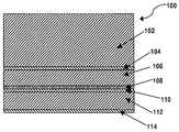
첨부된 도면들 중 도 1은 본 발명의 (일반적으로 도면부호 (100) 로 지정된) 제 1 다층 시트의 개략적인 단면도이다. 시트 (100) 는, 대략 2 mil (51 ㎛) 의 두께를 갖는 마스킹 막 (102) 및 그 마스킹 막 (102) 에 접촉하는 방현 하드 코트 (104) 를 포함한다. 최종 디스플레이가 사용되기 전에 제거되며 최종 디스플레이를 형성하기 위해 가요성 백플레인 (미도시) 에 시트 (100) 가 적층되기 전에 제거될 수도 있는 마스킹 막 (102) 은, 시트 (100) 의 생성 동안의 손상으로부터 하드 코트 (104) 를 보호하도록 기능한다. 또한, 마스킹 막 (102) 은 시트 (100) 의 두께 및 강성을 증가시키도록 기능함으로써, 시트 (100) 의 핸들링을 용이하게 한다.1 of the accompanying drawings is a schematic cross sectional view of a first multi-layered sheet (generally designated 100) of the present invention.
시트 (100) 는, 하드 코트 (104) 로부터 멀리 떨어진 표면 상에 알루미늄 옥 사이드 (AlOx) 장벽층 (108) 을 지지하는 0.5 mil (13 ㎛) 폴리(에틸렌 테레프탈레이트) (PET) 층 (106) 을 더 포함한다. 장벽층 (108) 은, 두번째의 0.5 mil (13 ㎛) 의 PET 층 (112) 에 장벽층 (108) 을 고정시키는 얇은 (대략 5 ㎛) 경화된 접착층 (110) 에 접촉한다. PET 층 (106) 과 다르게, PET (112) 는 자외선 흡수제를 함유한다. 마지막으로, 시트 (100) 는, 장벽층으로서 작용하며 또한 최종 디스플레이의 전면 전극을 형성하는 ITO 층 (114) 을 포함한다. 따라서, 시트 (100) 의 일방의 외부 표면 상에 ITO 층 (114) 이 존재하여 전기-광학 매체에 가능한 근접하게 놓일 수 있다. 대조적으로, 시트 (100) 의 구조는, 층들의 스택의 중간에, 2개의 PET 층들 (106 및 112) 사이에, AlOx 층 (108) 을 배치한다. 얇은 AlOx 층 (108) 의 이러한 배치는 이 장벽층에 대한 기계적인 손상의 기회를 감소시킨다.
도 1에 도시된 시트 (100) 를 제조하기 위한 바람직한 프로세스는 다음과 같다. PET 시트 (112) 에 자외선 흡수제가 통합되고, 결과의 UV-흡수 PET 층의 일방의 표면 상에 ITO 층 (114) 이 스퍼터링된다. 개별적으로, 두번째의 PET 시트 (106) 상에 AlOx 가 스퍼터링된다. 두번째의 PET 시트 (106) 의 AlOx-코팅된 표면 또는 첫번째의 PET 시트 (112) 의 비-ITO 코팅된 표면 중 어느 하나의 표면 상에 경화성 습윤 접착제 (110) 가 코팅되고, 도 1의 층들 (106 내지 114) 을 포함하는 서브-어셈블리를 형성하기 위해 2개의 PET 시트들이 함께 고정된다. 마지막으로, PET 층 (106) 의 노출된 표면 상에 방현 하드 코트 (104) 가 코팅되 며, 시트 (100) 의 핸들링 두께를 증가시키고 하드 코트 (104) 를 보호하기 위해 하드 코트 (104) 의 노출된 표면에 (통상적으로 롤 형태로 미리 형성된 막으로서 공급되는) 마스킹 막 (102) 이 도포된다.The preferred process for producing the
(제거가능한 마스킹 막 (102) 을 제외한) 시트 (100) 의 총 두께는 50 ㎛ 미만일 수 있다. 이전에 나타낸 바와 같이, 2개의 PET 층들 (106 및 112) 이 각각 0.5 mil 두께이므로, 이들의 총 두께는 1 mil 또는 25 ㎛ 이다. 접착층 (110) 은 약 5 ㎛ 의 두께이다. 방현 하드 코트 (104) 는 통상적으로 2 ㎛ 이하의 두께를 가질 것이다. 스퍼터링된 장벽층 (108) 및 ITO 층 (114) 은 각각 약 1 ㎛ 의 두께를 갖는다. 따라서, 시트 (100) 의 총 두께는 약 34 ㎛ 일 것이다. 종래의 롤-투-롤 (roll-to-roll) 동작들 동안 이러한 두께의 시트들을 다루는 것은 상당한 어려움들을 내포하고, 따라서 종래의 습윤 프로세싱 장비 상에서의 코팅의 어려움들을 감소시키는 두께를 갖는 시트를 제공하기 위해, 통상적으로 약 50 ㎛ 의 두께를 갖는 비교적 두꺼운 마스킹 시트가 바람직하다.The total thickness of the sheet 100 (except for the removable masking film 102) may be less than 50 μm. As previously shown, since the two
이러한 두께의 단일 시트에서 모든 필요한 장벽, 자외선 보호, 및 하드 코트 (기계적인 보호 및 방현) 기능들을 제공하기 위한 능력은, 종래 기술 설계들에서 통상적으로 가능한 것보다 훨씬 더 얇은 전기-광학 디스플레이들의 생성을 가능하게 하며, 개별적인 층들에 의해 시트 (100) 의 다양한 기능들이 제공된다. 이전에 설명된 바와 같이, 시트 (100) 는 약 34 ㎛ 의 두께를 가질 수도 있다. 통상적인 더블 릴리즈 막은, (최종 디스플레이에 더블 릴리즈 막이 통합되기 전에 당연히 제거되는 릴리즈 막들을 포함하지 않은) 약 56 ㎛ 의 총 두께에 대하여, (시트 (100) 에 적층되는) 25 ㎛ 의 접착층과 (백플레인에 적층되는) 6 ㎛ 의 접착층 사이에 개재된 25 ㎛ 의 전기영동 층을 포함할 수도 있다. 폴리머 막 상에 유기 반도체들을 인쇄함으로써, 필요한 어떤 추가적인 장벽층들도 포함하면서도, 약 25 ㎛ 이하의 총 두께를 갖는 백플레인들을 생성하는 것이 가능하다. 시트 (100), 그러한 더블 릴리즈 막, 및 백플레인으로부터 생성된 전기-광학 디스플레이는 약 115 ㎛ 의 총 두께를 가질 것이고, 상업적인 5 mil (127 ㎛) PET 막과 크게 상이하지 않은 물리적인 특성들을 가질 것이다. 따라서, 그러한 디스플레이는 (예컨대) 직경이 10 ㎜ 인 맨드렐에 용이하게 감겨질 수 있거나, 또는 유사한 두께의 셀룰러 전화기 또는 유사한 전자 디바이스에 감겨질 수 있다.The ability to provide all the necessary barrier, UV protection, and hard coat (mechanical protection and antiglare) functions in a single sheet of this thickness creates the production of electro-optical displays that are much thinner than normally possible in prior art designs. And various functions of the
도 1에 도시된 구조의 다수의 변형들이 가능하다. 원한다면 마스킹 막 (102) 이 생략될 수 있다. 몇몇 애플리케이션들에서, 하드 코트 (104) 를 생략하여, PET 층 (106) 의 일방의 표면을 시트 (100) 의 뷰잉 표면으로서 남기는 것이 또한 가능할 수도 있다. 자외선 방사에 사용되는 특정한 전기-광학 매체의 민감도 및 가능하게는 디스플레이의 의도된 사용 (예컨대, 실내 강의실 내의 디스플레이 스크린으로서 사용하도록 의도된 롤링 가능한 디스플레이는 자외선 보호를 필요로 하지 않을 수도 있다) 에 따라, PET 층 (112) 으로부터 자외선 흡수제가 생략될 수 있거나, 또는 상술된 제 2007/0109219호에서 설명된 바와 같이 다른 방식들로 자외선 흡수가 제공될 수 있다. AlOx 장벽층은, 충분한 투명도 및 장벽 특징들을 갖는 임의의 스퍼터링되거나 또는 증착된 (evaporated) 금속 또는 세라믹 층, 또는 폴리머에 의해 대체될 수 있으며; 적절한 재료들의 예들은 ITO, 알루미늄, 실리콘 옥사이드, 실리콘 카바이드, 및 등록 상표 CLARIS, ACLAR, 및 SARAN 하에서 상업적으로 판매되는 호모폴리머들을 포함할 수도 있다. 유사하게, ITO 층 (114) 은, 충분한 투명도 및 도전성을 갖는 임의의 스퍼터링되거나 또는 증착된 금속 또는 세라믹 층, 또는 폴리머에 의해 대체될 수 있으며; 적절한 재료들의 예들은 알루미늄, PEDOT (poly(3,4-ethylenedioxythiophene)) 와 같은 도전성 폴리머, 및 카본 나노튜브들을 포함할 수도 있다.Many variations of the structure shown in FIG. 1 are possible. Masking
AlOx 층 (108) 과 ITO 층 (114) 의 조합은 어느 하나의 층 단독보다 더 효과적인 장벽층을 제공한다. 스퍼터링된 막들의 장벽 특징들은 스퍼터링된 층에 필연적으로 존재하는 작은 핀홀들에 의해 제한된다. 상술된 바와 같은 시트 (100) 의 제조에서 이루어지는 바와 같이, 2개의 스퍼터링된 막들을 함께 적층함으로써, 2개의 장벽층들에서 랜덤으로 분포된 핀홀들의 중첩 (superposition) 이 거의 없는 리던던트 (redundant) 장벽층이 형성된다.The combination of AlOx layer 108 and
시트 (100) 는 또한 기계적으로 내구성이 좋다. 기계적인 응력은 AlOx 및 ITO 장벽층들에서 크랙들을 야기하려는 경향이 있지만, 리던던트 장벽층들의 존재, 및 얇은 접착층에 의해 분리된 상이한 폴리머 (PET) 막들에 그러한 장벽층들이 도포되는 사실은 2개의 장벽층들에서 서로로부터 크랙들의 발생을 디커플링 (decouple) 하려는 경향이 있다. (마스킹 막 (102) 을 포함하거나 또는 포함하지 않은) 도 1에 도시된 시트 (100) 는, 임의의 롤링 이전의 시트에 관련한 장벽 특징들에서 어떠한 감소도 보이지 않으면서 15 ㎜ 직경의 맨드렐에 10,000 회 감겨졌다.The
상기 논의가 주로 약 25 ㎛ 의 두께를 갖는 매우 얇은 전면 서브-어셈블리들에 관한 것이었지만, 서브-어셈블리의 두께를 증가시킴으로써 추가적인 충격 보호가 추가될 수 있다. 이는, 추가적인 층들 (예컨대, PET, PEN, 또는 폴리카보네이트 (polycarbonate)) 을 적층하거나 또는 접착 및 장벽 층들과 같은 더 두꺼운 보조층들을 제공하여, PET 층들의 하나 또는 양자 모두의 두께를 증가시킴으로써 실시될 수 있다.Although the above discussion is mainly about very thin front sub-assemblies having a thickness of about 25 μm, additional impact protection can be added by increasing the thickness of the sub-assemblies. This can be done by stacking additional layers (eg, PET, PEN, or polycarbonate) or by providing thicker auxiliary layers such as adhesive and barrier layers to increase the thickness of one or both PET layers. Can be.
시트 (100) 의 특징들과 유사한 특징들을 갖는 본질적으로 모놀리식의 비-적층된 시트가, 원한다면 방현 하드 코트를 코팅하고 마스킹 막을 도포하여, 폴리머 층 내에 또는 비-전극 장벽층 (즉, 시트 (100) 내의 AlOx 층) 위의 추가적인 코팅으로서 자외선 흡수제가 제공되면서, 단일 폴리머 층의 대향측들 상에 2개의 장벽층들을 스퍼터링함으로써 생성될 수 있다는 것이 일견에 나타날 수도 있다. 그러나, 그러한 프로세스는, 스퍼터링 및 코팅 단계들이 동일한 폴리머 층 상에 순차적으로 수행되므로, 다양한 단계들에서 수율 손실이 악화된다는 심각한 손해를 가지며, 이는 결과의 시트를 고가가 되게 할 것이다. 또한, 국부적으로 불량한 장벽 특징들을 응집 (nucleate) 하는 폴리머 층 내의 결함들은, 장벽 특징들이 잘 훼손 (compromise) 될 수도 있도록, 동일한 폴리머 층의 양측들 상의 장벽층들에 영향을 미칠 것이다. 유사하게, 기계적인 응력으로 인한 크랙들은 장벽층들 양자 모두에서 동일한 위치에서 발생할 것이다.An essentially monolithic non-laminated sheet having characteristics similar to those of the
첨부 도면들 중 도 2는 본 발명의 (일반적으로 도면부호 (200) 로 지정된) 제 2 다층 시트의 개략적인 단면도이다. 시트 (200) 는 대략 2 mil (51 ㎛) 의 두께를 갖는 마스킹 막 (202) 및 그 마스킹 막 (202) 에 접촉하는 방현 하드 코트 (204) 를 포함한다. 마스킹 막 (202) 및 하드 코트 (204) 양자 모두는 도 1에 도시된 시트 (100) 의 대응하는 층들과 동일하고 동일한 기능들을 제공한다. 시트 (200) 는 0.5 mil (13 ㎛) 폴리(에틸렌 테레프탈레이트) (PET) 층 (206) 을 더 포함하고; 그러나, 시트 (200) 에서, 이 층 (206) 이 자외선 흡수제를 보유한다. 하드 코트 (204) 로부터 멀리 떨어진 층 (206) 의 표면은, 얇은 (대략 5 ㎛) 경화된 접착층 (210) 에 의해 두번째의 AlOx 장벽층 (208B) 에 고정된 AlOx 장벽층 (208A) 을 지지한다. 장벽층 (208B) 은 두번째의 0.5 mil (13 ㎛) PET 층 (212) 상에 지지된다. 마지막으로, 시트 (200) 는, 최종 디스플레이의 전면 전극을 형성하는 습윤 코팅된 도전층 (214) 을 포함한다.2 of the accompanying drawings is a schematic cross-sectional view of a second multi-layer sheet (generally designated 200) of the present invention. The
도 2에 도시된 시트 (200) 를 제조하기 위한 바람직한 프로세스는 다음과 같다. 프로세스는, 그 위에 이미 형성된 AlOx 층을 갖는 PET의 2개의 시트들로부터 시작하며; AlOx 코팅들을 지지하는 그러한 PET 시트들은 용이하게 상업적으로 입수가능하며, 2개의 시트들은 결국 최종 시트 (200) 의 층들 (206/208A 및 212/208B) 을 형성할 것이다. AlOx 코팅들 중 하나 상에 경화성 습윤 접착제가 코팅되고, 시트 (200) 의 층들 (206/208A/210/208B/212) 을 형성하기 위해 2개의 PET/AlOx 가 합쳐지고 접착 경화된다. PET 층 (206) 에 자외선 흡수제가 확산되고, 두번째의 PET 시트 (212) 의 일방의 표면 상에 도전층 (214) 이 습윤 코팅된다. 마지막으로, PET 층 (206) 의 노출된 표면 상에 방현 하드 코트 (204) 가 코팅되고, 그 후 하드 코트 (204) 의 노출된 표면에 마스킹 막 (202) 이 도포된다.A preferred process for producing the
시트 (200) 에서, 2개의 PET 층들 사이에 AlOx 장벽층들 (208A 및 208B) 이 매립되고, 따라서 기계적인 손상으로부터 잘 보호된다.In the
도 1에 도시된 시트 (100) 에서와 같이, 도 2에 도시된 시트 (200) 의 다수의 변형들이 가능하다. 시트 (100) 에 대해 언급된 모든 변형들이 또한 시트 (200) 에서 실시될 수 있다. 또한, 어느 하나의 PET 층에 자외선 흡수제가 통합될 수 있다. 원한다면 마스킹 막 (202) 이 생략될 수 있다. 몇몇 애플리케이션들에서, 하드 코트 (204) 를 생략하여, PET 층 (206) 의 일방의 표면을 시트 (200) 의 뷰잉 표면으로서 남기는 것이 또한 가능할 수도 있다. 자외선 방사에 사용되는 특정한 전기-광학 매체의 민감도 및 가능하게는 디스플레이의 의도된 사용에 따라, PET 층 (206) 으로부터 자외선 흡수제가 생략될 수 있거나, 또는 상술된 제 2007/0109219호에서 설명된 바와 같은 다른 방식들로 자외선 흡수가 제공될 수 있다. AlOx 장벽층은, 충분한 투명도 및 장벽 특징들을 갖는 임의의 스퍼터링되거나 또는 증착된 금속 또는 세라믹 층, 또는 폴리머에 의해 대체될 수 있으며; 적절한 재료들의 예들은 ITO, 알루미늄, 실리콘 옥사이드, 실리콘 카바이드, 및 등록 상표 CLARIS, ACLAR, 및 SARAN 하에서 상업적으로 판매되는 호모폴리머들을 포함할 수도 있다. 유사하게, 도전층 (214) 은 충분한 투명도 및 도전성을 갖는 임의의 스퍼터링되거나 또는 증착된 금속 또는 세라믹 층, 또는 폴리머에 의해 대체될 수 있으며, 적절한 재료들의 예들은 알루미늄, PEDOT (poly(3,4-ethylenedioxythiophene)) 와 같은 도전성 폴리머, 및 카본 나노튜브들을 포함할 수도 있다. 시트 (200) 에서, 어셈블리의 순서는 수율 손실을 감소시키는데 중요하다.As in the
상술된 바와 같이, 도 1에 도시된 시트 (100) 에서, ITO 층 (114) 은 도전 및 장벽 기능들 양자 모두를 제공한다. 대조적으로, 시트 (200) 에서 층 (214) 과 같은 습윤 프로세싱된 도전층들은 통상적으로 불량한 장벽 특징들을 갖는다. 따라서, 우수한 장벽 특징들을 보존하기 위해서는, 시트 (100) 에서의 AlOx 층 (108) 과 ITO 층 (114) 의 조합에 의해 제공되는 장벽 특징들과 유사한 장벽 특징들을 제공하기 위해, 시트 (200) 에 (시트 (100) 에서의 단일 AlOx 층 (108) 과 대조적으로) 2개의 AlOx 층들 (208A 및 208B) 이 제공된다. 시트 (200) 에 2개의 AlOx 층들 (208A 및 208B) 을 제공하는 것은, AlOx 코팅된 폴리머 막이 비교적 저가이고 반면에 ITO는 고가이므로, 경제적으로 실용적이다. 시트 (200) 의 기계적인 특징들은 막 (100) 의 기계적인 특징들과 매우 유사하다.As described above, in the
상술된 바로부터, 본 발명이 전기-광학 디스플레이에서 사용하기 위한 우수한 장벽 특징들을 갖는 기계적으로 강건한 전면 서브-어셈블리를 제공할 수 있다는 것을 알게 될 것이다. 방현 하드 코트, 자외선 흡수제, (존재한다면) 채용된 마스킹 막의 두께 및 타입과 같은 특징들은 개별적인 커스토머 요구조건들에 적합화하기 위해 용이하게 변경될 수 있다.From the foregoing, it will be appreciated that the present invention can provide a mechanically robust frontside sub-assembly with excellent barrier features for use in electro-optical displays. Features such as anti-glare hard coat, ultraviolet absorber, and thickness and type of masking film employed (if present) can be easily modified to suit individual customer requirements.
선행하는 논의로부터, 본 발명의 막들이 막이 접착할 수 있는 고체 외부 표면을 갖는 임의의 전기-광학층과 함께 사용될 수 있다는 것이 명백하게 될 것이다. 따라서, 본 방법들은 임의의 타입의 상술된 전기-광학 매체들을 사용하여 수행될 수 있다. 예컨대, 본 방법들은 회전 이색성 멤버, 일렉트로크로믹 또는 전기영동 매체들을 사용할 수 있고, 마지막 경우에서 전기 영동 매체들은 캡슐형, 폴리머-분산형, 또는 마이크로셀 타입들로 이루어질 수도 있다. 본 발명의 막들을 사용하여 생성된 디스플레이들은 종래 기술의 고체 전기-광학 디스플레이들이 사용된 임의의 애플리케이션에서 사용될 수도 있다. 따라서, 예컨대, 본 디스플레이들은, 전자 북 판독기, 휴대용 컴퓨터, 타블렛 컴퓨터, 셀룰러 전화기, 스마트 카드, 사인 (sign), 시계, 선반 라벨, 및 플래시 드라이브에서 사용될 수도 있다.From the preceding discussion, it will be apparent that the films of the present invention can be used with any electro-optical layer having a solid outer surface to which the film can adhere. Thus, the methods can be performed using any type of electro-optical media described above. For example, the present methods may use rotating dichroic members, electrochromic or electrophoretic media, and in the last case the electrophoretic media may consist of capsule, polymer-disperse, or microcell types. Displays produced using the films of the present invention may be used in any application in which solid state electro-optical displays of the prior art are used. Thus, for example, the displays may be used in electronic book readers, portable computers, tablet computers, cellular telephones, smart cards, signs, watches, shelf labels, and flash drives.
Claims (17)
Translated fromKoreanApplications Claiming Priority (3)
| Application Number | Priority Date | Filing Date | Title |
|---|---|---|---|
| US88600507P | 2007-01-22 | 2007-01-22 | |
| US60/886,005 | 2007-01-22 | ||
| PCT/US2008/051629WO2008091850A2 (en) | 2007-01-22 | 2008-01-22 | Multi-layer sheet for use in electro-optic displays |
Publications (2)
| Publication Number | Publication Date |
|---|---|
| KR20090102823A KR20090102823A (en) | 2009-09-30 |
| KR101256709B1true KR101256709B1 (en) | 2013-04-19 |
Family
ID=39640917
Family Applications (1)
| Application Number | Title | Priority Date | Filing Date |
|---|---|---|---|
| KR1020097015374AActiveKR101256709B1 (en) | 2007-01-22 | 2008-01-22 | Multi-layer sheet for use in electro-optic displays |
Country Status (6)
| Country | Link |
|---|---|
| US (3) | US7667886B2 (en) |
| EP (1) | EP2111562B1 (en) |
| KR (1) | KR101256709B1 (en) |
| CN (1) | CN101836167B (en) |
| TW (1) | TWI386313B (en) |
| WO (1) | WO2008091850A2 (en) |
Families Citing this family (98)
| Publication number | Priority date | Publication date | Assignee | Title |
|---|---|---|---|---|
| US7999787B2 (en) | 1995-07-20 | 2011-08-16 | E Ink Corporation | Methods for driving electrophoretic displays using dielectrophoretic forces |
| US7848006B2 (en)* | 1995-07-20 | 2010-12-07 | E Ink Corporation | Electrophoretic displays with controlled amounts of pigment |
| US7583251B2 (en) | 1995-07-20 | 2009-09-01 | E Ink Corporation | Dielectrophoretic displays |
| US8040594B2 (en) | 1997-08-28 | 2011-10-18 | E Ink Corporation | Multi-color electrophoretic displays |
| DE69920228T2 (en)* | 1998-07-08 | 2005-01-27 | E-Ink Corp., Cambridge | METHOD FOR IMPROVING COLOR REPRODUCTION IN ELECTROPHORETIC DEVICES USING MICROCAPSULES |
| AU2002250304A1 (en)* | 2001-03-13 | 2002-09-24 | E Ink Corporation | Apparatus for displaying drawings |
| US8390918B2 (en) | 2001-04-02 | 2013-03-05 | E Ink Corporation | Electrophoretic displays with controlled amounts of pigment |
| US7679814B2 (en) | 2001-04-02 | 2010-03-16 | E Ink Corporation | Materials for use in electrophoretic displays |
| US20090009852A1 (en)* | 2001-05-15 | 2009-01-08 | E Ink Corporation | Electrophoretic particles and processes for the production thereof |
| US7223672B2 (en)* | 2002-04-24 | 2007-05-29 | E Ink Corporation | Processes for forming backplanes for electro-optic displays |
| US8363299B2 (en)* | 2002-06-10 | 2013-01-29 | E Ink Corporation | Electro-optic displays, and processes for the production thereof |
| US20040031167A1 (en)* | 2002-06-13 | 2004-02-19 | Stein Nathan D. | Single wafer method and apparatus for drying semiconductor substrates using an inert gas air-knife |
| US7839564B2 (en)* | 2002-09-03 | 2010-11-23 | E Ink Corporation | Components and methods for use in electro-optic displays |
| US20130063333A1 (en) | 2002-10-16 | 2013-03-14 | E Ink Corporation | Electrophoretic displays |
| US8177942B2 (en) | 2003-11-05 | 2012-05-15 | E Ink Corporation | Electro-optic displays, and materials for use therein |
| US20110164301A1 (en) | 2003-11-05 | 2011-07-07 | E Ink Corporation | Electro-optic displays, and materials for use therein |
| US11250794B2 (en) | 2004-07-27 | 2022-02-15 | E Ink Corporation | Methods for driving electrophoretic displays using dielectrophoretic forces |
| US7843624B2 (en) | 2006-03-08 | 2010-11-30 | E Ink Corporation | Electro-optic displays, and materials and methods for production thereof |
| US8390301B2 (en)* | 2006-03-08 | 2013-03-05 | E Ink Corporation | Electro-optic displays, and materials and methods for production thereof |
| US7688497B2 (en) | 2007-01-22 | 2010-03-30 | E Ink Corporation | Multi-layer sheet for use in electro-optic displays |
| KR101256709B1 (en) | 2007-01-22 | 2013-04-19 | 이 잉크 코포레이션 | Multi-layer sheet for use in electro-optic displays |
| JP4503030B2 (en)* | 2007-02-13 | 2010-07-14 | セイコーエプソン株式会社 | Method for storing microcapsules for electrophoretic display device |
| US7826129B2 (en) | 2007-03-06 | 2010-11-02 | E Ink Corporation | Materials for use in electrophoretic displays |
| US8034209B2 (en)* | 2007-06-29 | 2011-10-11 | E Ink Corporation | Electro-optic displays, and materials and methods for production thereof |
| US20090122389A1 (en) | 2007-11-14 | 2009-05-14 | E Ink Corporation | Electro-optic assemblies, and adhesives and binders for use therein |
| WO2009103857A1 (en)* | 2008-02-21 | 2009-08-27 | Marisense Oy | Display module and related manufacturing method |
| KR101237263B1 (en)* | 2008-03-21 | 2013-02-27 | 이 잉크 코포레이션 | Electro-optic displays and color filters |
| KR101214877B1 (en)* | 2008-04-11 | 2012-12-24 | 이 잉크 코포레이션 | Methods for driving electro-optic displays |
| TWI484273B (en)* | 2009-02-09 | 2015-05-11 | E Ink Corp | Electrophoretic particles |
| US8098418B2 (en)* | 2009-03-03 | 2012-01-17 | E. Ink Corporation | Electro-optic displays, and color filters for use therein |
| CN102687103B (en) | 2009-10-28 | 2016-04-20 | 伊英克公司 | Electro-optic display with touch sensor |
| US8654436B1 (en) | 2009-10-30 | 2014-02-18 | E Ink Corporation | Particles for use in electrophoretic displays |
| US20110195187A1 (en)* | 2010-02-10 | 2011-08-11 | Apple Inc. | Direct liquid vaporization for oleophobic coatings |
| US8446664B2 (en) | 2010-04-02 | 2013-05-21 | E Ink Corporation | Electrophoretic media, and materials for use therein |
| TWI484275B (en) | 2010-05-21 | 2015-05-11 | E Ink Corp | Electro-optic display, method for driving the same and microcavity electrophoretic display |
| TWI405020B (en)* | 2010-05-26 | 2013-08-11 | Au Optronics Corp | Electrophoretic display |
| US20130188324A1 (en)* | 2010-09-29 | 2013-07-25 | Posco | Method for Manufacturing a Flexible Electronic Device Using a Roll-Shaped Motherboard, Flexible Electronic Device, and Flexible Substrate |
| US8715779B2 (en)* | 2011-06-24 | 2014-05-06 | Apple Inc. | Enhanced glass impact durability through application of thin films |
| DE102011079101A1 (en)* | 2011-07-13 | 2013-01-17 | Osram Opto Semiconductors Gmbh | ORGANIC OPTOELECTRONIC COMPONENT AND METHOD FOR THE PRODUCTION THEREOF |
| US9087488B1 (en)* | 2011-09-15 | 2015-07-21 | Amazon Technologies, Inc. | Producing electro-optic display with seamless front surface |
| US20130314774A1 (en)* | 2011-11-16 | 2013-11-28 | Cool Earth Solar Inc. | Inflated tubular solar concentrators |
| CN103137245B (en)* | 2011-11-30 | 2015-09-09 | 群康科技(深圳)有限公司 | Nesa coating and manufacture method, electronic installation |
| US11467466B2 (en) | 2012-04-20 | 2022-10-11 | E Ink Corporation | Illumination systems for reflective displays |
| US10190743B2 (en) | 2012-04-20 | 2019-01-29 | E Ink Corporation | Illumination systems for reflective displays |
| WO2014110394A1 (en) | 2013-01-10 | 2014-07-17 | E Ink Corporation | Electro-optic display with controlled electrochemical reactions |
| US9715155B1 (en) | 2013-01-10 | 2017-07-25 | E Ink Corporation | Electrode structures for electro-optic displays |
| WO2014209300A1 (en)* | 2013-06-26 | 2014-12-31 | Empire Technology Development Llc | Electrophoretic displays having charged fluorescent dendrimer particles |
| US10317767B2 (en) | 2014-02-07 | 2019-06-11 | E Ink Corporation | Electro-optic display backplane structure with drive components and pixel electrodes on opposed surfaces |
| HK1225848A1 (en) | 2014-02-07 | 2017-09-15 | 伊英克公司 | Electro-optic display backplane structures |
| US10446585B2 (en) | 2014-03-17 | 2019-10-15 | E Ink Corporation | Multi-layer expanding electrode structures for backplane assemblies |
| KR20150110848A (en)* | 2014-03-20 | 2015-10-05 | 삼성디스플레이 주식회사 | Display device |
| US10901125B2 (en) | 2014-05-23 | 2021-01-26 | Eyesafe, Llc | Light emission reducing compounds for electronic devices |
| US10642087B2 (en) | 2014-05-23 | 2020-05-05 | Eyesafe, Llc | Light emission reducing compounds for electronic devices |
| WO2016073914A1 (en) | 2014-11-07 | 2016-05-12 | E Ink Corporation | Applications of electro-optic displays |
| US9835925B1 (en) | 2015-01-08 | 2017-12-05 | E Ink Corporation | Electro-optic displays, and processes for the production thereof |
| US9684339B2 (en) | 2015-02-03 | 2017-06-20 | Microsoft Technology Licensing, Llc | Bendable display assembly |
| US10997930B2 (en) | 2015-05-27 | 2021-05-04 | E Ink Corporation | Methods and circuitry for driving display devices |
| CN113759630B (en) | 2015-06-29 | 2024-04-26 | 伊英克公司 | Method for mechanically and electrically connecting to display electrodes |
| JP2017032666A (en)* | 2015-07-29 | 2017-02-09 | セイコーエプソン株式会社 | Electrophoretic display device and electronic apparatus |
| US10527899B2 (en) | 2016-05-31 | 2020-01-07 | E Ink Corporation | Backplanes for electro-optic displays |
| JP6876727B2 (en) | 2016-06-10 | 2021-05-26 | イー インク コーポレイション | Electro-optic display device |
| US10324577B2 (en) | 2017-02-28 | 2019-06-18 | E Ink Corporation | Writeable electrophoretic displays including sensing circuits and styli configured to interact with sensing circuits |
| EP3602193A4 (en) | 2017-03-28 | 2021-01-06 | E Ink Corporation | POROUS BACK PANEL FOR ELECTRO-OPTICAL DISPLAY |
| CN112860018B (en) | 2017-05-19 | 2024-12-27 | 伊英克公司 | Foldable electro-optical display with digitization and touch sensing |
| KR20190133292A (en) | 2017-05-30 | 2019-12-02 | 이 잉크 코포레이션 | Electro-optic displays |
| US11404013B2 (en) | 2017-05-30 | 2022-08-02 | E Ink Corporation | Electro-optic displays with resistors for discharging remnant charges |
| US10241377B1 (en)* | 2017-09-18 | 2019-03-26 | Amazon Technologies, Inc. | Self-healing flexible electrophoretic displays |
| US10882042B2 (en) | 2017-10-18 | 2021-01-05 | E Ink Corporation | Digital microfluidic devices including dual substrates with thin-film transistors and capacitive sensing |
| US10824042B1 (en) | 2017-10-27 | 2020-11-03 | E Ink Corporation | Electro-optic display and composite materials having low thermal sensitivity for use therein |
| EP4137884B1 (en) | 2017-11-03 | 2025-05-28 | E Ink Corporation | Processes for producing electro-optic displays |
| US11081066B2 (en) | 2018-02-15 | 2021-08-03 | E Ink Corporation | Via placement for slim border electro-optic display backplanes with decreased capacitive coupling between t-wires and pixel electrodes |
| US11175561B1 (en) | 2018-04-12 | 2021-11-16 | E Ink Corporation | Electrophoretic display media with network electrodes and methods of making and using the same |
| KR102387849B1 (en)* | 2018-05-17 | 2022-04-15 | 이 잉크 캘리포니아 엘엘씨 | Piezo Electrophoresis Display |
| TWI727374B (en)* | 2018-07-25 | 2021-05-11 | 美商電子墨水股份有限公司 | Flexible transparent intumescent coatings and composites incorporating the same |
| CN109062446A (en)* | 2018-09-11 | 2018-12-21 | 深圳市易快来科技股份有限公司 | It is a kind of to touch aobvious device and its manufacturing method |
| US11353759B2 (en) | 2018-09-17 | 2022-06-07 | Nuclera Nucleics Ltd. | Backplanes with hexagonal and triangular electrodes |
| TWI763526B (en) | 2018-10-15 | 2022-05-01 | 美商電子墨水股份有限公司 | Method for dispensing an aqueous chemical species to a surface |
| US11145262B2 (en) | 2018-11-09 | 2021-10-12 | E Ink Corporation | Electro-optic displays |
| US11592701B2 (en) | 2018-11-28 | 2023-02-28 | Eyesafe Inc. | Backlight unit with emission modification |
| US12321060B1 (en) | 2018-11-28 | 2025-06-03 | Eyesafe Inc. | Color filter enhancements for display devices |
| US10955697B2 (en) | 2018-11-28 | 2021-03-23 | Eyesafe Inc. | Light emission modification |
| US11810532B2 (en) | 2018-11-28 | 2023-11-07 | Eyesafe Inc. | Systems for monitoring and regulating harmful blue light exposure from digital devices |
| US11126033B2 (en) | 2018-11-28 | 2021-09-21 | Eyesafe Inc. | Backlight unit with emission modification |
| CN113168005B (en) | 2018-12-13 | 2023-05-02 | 伊英克公司 | Illumination system for reflective display |
| TWI728631B (en) | 2018-12-28 | 2021-05-21 | 美商電子墨水股份有限公司 | Electro-optic displays |
| CN113228151B (en) | 2018-12-30 | 2024-03-29 | 伊英克公司 | electro-optical display |
| US10971660B2 (en) | 2019-08-09 | 2021-04-06 | Eyesafe Inc. | White LED light source and method of making same |
| KR102721288B1 (en)* | 2019-12-23 | 2024-10-23 | 이 잉크 코포레이션 | Transferable light-transmitting electrode film for electro-optical devices |
| WO2021158744A1 (en) | 2020-02-07 | 2021-08-12 | E Ink Corporation | Electrophoretic display layer with thin film top electrode |
| JP7506769B2 (en) | 2020-06-03 | 2024-06-26 | イー インク コーポレイション | Foldable electrophoretic display module including a non-conductive support plate - Patents.com |
| WO2022035570A1 (en) | 2020-08-12 | 2022-02-17 | Eastman Chemical Company | Transparent conductive barrier films |
| EP4388370A4 (en) | 2021-08-18 | 2025-07-02 | E Ink Corp | METHOD FOR CONTROLLING ELECTRO-OPTICAL DISPLAYS |
| WO2023164099A1 (en) | 2022-02-28 | 2023-08-31 | E Ink Corporation | Parking space management system |
| US11830449B2 (en) | 2022-03-01 | 2023-11-28 | E Ink Corporation | Electro-optic displays |
| EP4540656B1 (en) | 2023-08-30 | 2025-10-15 | E Ink Corporation | An electro-optic device having electrophoretic medium comprising an organic electroactive compound |
| WO2025096260A1 (en) | 2023-10-31 | 2025-05-08 | E Ink Corporation | A color electro-optic display comprising a light fastness additive |
| US20250224645A1 (en) | 2024-01-05 | 2025-07-10 | E Ink Corporation | Electrophoretic medium comprising particles having a pigment core and a polymeric shell |
| US20250224646A1 (en) | 2024-01-08 | 2025-07-10 | E Ink Corporation | Adhesive Layer Comprising Conductive Filler Particles and a Polymeric Dispersant |
Citations (4)
| Publication number | Priority date | Publication date | Assignee | Title |
|---|---|---|---|---|
| US6097531A (en)* | 1998-11-25 | 2000-08-01 | Xerox Corporation | Method of making uniformly magnetized elements for a gyricon display |
| US6407847B1 (en)* | 2000-07-25 | 2002-06-18 | Gentex Corporation | Electrochromic medium having a color stability |
| US20040027327A1 (en)* | 2002-06-10 | 2004-02-12 | E Ink Corporation | Components and methods for use in electro-optic displays |
| JP2004151528A (en)* | 2002-10-31 | 2004-05-27 | Bridgestone Corp | Barrier film for protecting thin-film display elements |
Family Cites Families (236)
| Publication number | Priority date | Publication date | Assignee | Title |
|---|---|---|---|---|
| NL7005615A (en) | 1969-04-23 | 1970-10-27 | ||
| US3870517A (en) | 1969-10-18 | 1975-03-11 | Matsushita Electric Industrial Co Ltd | Color image reproduction sheet employed in photoelectrophoretic imaging |
| US3668106A (en) | 1970-04-09 | 1972-06-06 | Matsushita Electric Industrial Co Ltd | Electrophoretic display device |
| US3767392A (en) | 1970-04-15 | 1973-10-23 | Matsushita Electric Industrial Co Ltd | Electrophoretic light image reproduction process |
| US3792308A (en) | 1970-06-08 | 1974-02-12 | Matsushita Electric Industrial Co Ltd | Electrophoretic display device of the luminescent type |
| JPS4917079B1 (en) | 1970-12-21 | 1974-04-26 | ||
| US4418346A (en) | 1981-05-20 | 1983-11-29 | Batchelder J Samuel | Method and apparatus for providing a dielectrophoretic display of visual information |
| US4640583A (en) | 1983-07-22 | 1987-02-03 | Kabushiki Kaisha Seiko Epson | Display panel having an inner and an outer seal and process for the production thereof |
| US4857393A (en) | 1987-06-19 | 1989-08-15 | Toppan Printing Co., Ltd. | Waterproof water-vapor-permeable laminated structure and applications of the same |
| DE69416228T2 (en) | 1993-09-30 | 1999-06-24 | Toppan Printing Co. Ltd., Tokio/Tokyo | Gas impermeable laminate |
| US5745094A (en) | 1994-12-28 | 1998-04-28 | International Business Machines Corporation | Electrophoretic display |
| US6137467A (en) | 1995-01-03 | 2000-10-24 | Xerox Corporation | Optically sensitive electric paper |
| US7327511B2 (en) | 2004-03-23 | 2008-02-05 | E Ink Corporation | Light modulators |
| US7071913B2 (en) | 1995-07-20 | 2006-07-04 | E Ink Corporation | Retroreflective electrophoretic displays and materials for making the same |
| US7411719B2 (en) | 1995-07-20 | 2008-08-12 | E Ink Corporation | Electrophoretic medium and process for the production thereof |
| US6124851A (en) | 1995-07-20 | 2000-09-26 | E Ink Corporation | Electronic book with multiple page displays |
| US7583251B2 (en) | 1995-07-20 | 2009-09-01 | E Ink Corporation | Dielectrophoretic displays |
| US6664944B1 (en) | 1995-07-20 | 2003-12-16 | E-Ink Corporation | Rear electrode structures for electrophoretic displays |
| US7259744B2 (en) | 1995-07-20 | 2007-08-21 | E Ink Corporation | Dielectrophoretic displays |
| US7848006B2 (en) | 1995-07-20 | 2010-12-07 | E Ink Corporation | Electrophoretic displays with controlled amounts of pigment |
| US6120839A (en) | 1995-07-20 | 2000-09-19 | E Ink Corporation | Electro-osmotic displays and materials for making the same |
| US7106296B1 (en) | 1995-07-20 | 2006-09-12 | E Ink Corporation | Electronic book with multiple page displays |
| US6639578B1 (en) | 1995-07-20 | 2003-10-28 | E Ink Corporation | Flexible displays |
| US6710540B1 (en) | 1995-07-20 | 2004-03-23 | E Ink Corporation | Electrostatically-addressable electrophoretic display |
| US7109968B2 (en) | 1995-07-20 | 2006-09-19 | E Ink Corporation | Non-spherical cavity electrophoretic displays and methods and materials for making the same |
| US6118426A (en) | 1995-07-20 | 2000-09-12 | E Ink Corporation | Transducers and indicators having printed displays |
| US6515649B1 (en) | 1995-07-20 | 2003-02-04 | E Ink Corporation | Suspended particle displays and materials for making the same |
| US7956841B2 (en) | 1995-07-20 | 2011-06-07 | E Ink Corporation | Stylus-based addressing structures for displays |
| US7999787B2 (en) | 1995-07-20 | 2011-08-16 | E Ink Corporation | Methods for driving electrophoretic displays using dielectrophoretic forces |
| US7193625B2 (en) | 1999-04-30 | 2007-03-20 | E Ink Corporation | Methods for driving electro-optic displays, and apparatus for use therein |
| US6866760B2 (en) | 1998-08-27 | 2005-03-15 | E Ink Corporation | Electrophoretic medium and process for the production thereof |
| US6262706B1 (en) | 1995-07-20 | 2001-07-17 | E Ink Corporation | Retroreflective electrophoretic displays and materials for making the same |
| US8089453B2 (en) | 1995-07-20 | 2012-01-03 | E Ink Corporation | Stylus-based addressing structures for displays |
| US20050012980A1 (en) | 2003-05-02 | 2005-01-20 | E Ink Corporation | Electrophoretic displays with controlled amounts of pigment |
| US7304634B2 (en) | 1995-07-20 | 2007-12-04 | E Ink Corporation | Rear electrode structures for electrophoretic displays |
| US6459418B1 (en) | 1995-07-20 | 2002-10-01 | E Ink Corporation | Displays combining active and non-active inks |
| US8139050B2 (en) | 1995-07-20 | 2012-03-20 | E Ink Corporation | Addressing schemes for electronic displays |
| US6017584A (en) | 1995-07-20 | 2000-01-25 | E Ink Corporation | Multi-color electrophoretic displays and materials for making the same |
| US6120588A (en) | 1996-07-19 | 2000-09-19 | E Ink Corporation | Electronically addressable microencapsulated ink and display thereof |
| US7167155B1 (en) | 1995-07-20 | 2007-01-23 | E Ink Corporation | Color electrophoretic displays |
| US6727881B1 (en) | 1995-07-20 | 2004-04-27 | E Ink Corporation | Encapsulated electrophoretic displays and methods and materials for making the same |
| US7352353B2 (en) | 1995-07-20 | 2008-04-01 | E Ink Corporation | Electrostatically addressable electrophoretic display |
| US7079305B2 (en) | 2001-03-19 | 2006-07-18 | E Ink Corporation | Electrophoretic medium and process for the production thereof |
| US5760761A (en) | 1995-12-15 | 1998-06-02 | Xerox Corporation | Highlight color twisting ball display |
| US5808783A (en) | 1996-06-27 | 1998-09-15 | Xerox Corporation | High reflectance gyricon display |
| US6055091A (en) | 1996-06-27 | 2000-04-25 | Xerox Corporation | Twisting-cylinder display |
| US6721083B2 (en) | 1996-07-19 | 2004-04-13 | E Ink Corporation | Electrophoretic displays using nanoparticles |
| US6323989B1 (en) | 1996-07-19 | 2001-11-27 | E Ink Corporation | Electrophoretic displays using nanoparticles |
| DE69636960C5 (en) | 1996-07-19 | 2015-07-30 | E-Ink Corp. | Electronically addressable microencapsulated ink |
| US6538801B2 (en) | 1996-07-19 | 2003-03-25 | E Ink Corporation | Electrophoretic displays using nanoparticles |
| US5930026A (en) | 1996-10-25 | 1999-07-27 | Massachusetts Institute Of Technology | Nonemissive displays and piezoelectric power supplies therefor |
| US5777782A (en) | 1996-12-24 | 1998-07-07 | Xerox Corporation | Auxiliary optics for a twisting ball display |
| AU6004798A (en) | 1997-02-06 | 1998-08-26 | University College Dublin | Electrochromic system |
| US6980196B1 (en) | 1997-03-18 | 2005-12-27 | Massachusetts Institute Of Technology | Printable electronic display |
| US5961804A (en) | 1997-03-18 | 1999-10-05 | Massachusetts Institute Of Technology | Microencapsulated electrophoretic display |
| US6839158B2 (en) | 1997-08-28 | 2005-01-04 | E Ink Corporation | Encapsulated electrophoretic displays having a monolayer of capsules and materials and methods for making the same |
| US7247379B2 (en) | 1997-08-28 | 2007-07-24 | E Ink Corporation | Electrophoretic particles, and processes for the production thereof |
| US6232950B1 (en) | 1997-08-28 | 2001-05-15 | E Ink Corporation | Rear electrode structures for displays |
| US6300932B1 (en) | 1997-08-28 | 2001-10-09 | E Ink Corporation | Electrophoretic displays with luminescent particles and materials for making the same |
| US7002728B2 (en) | 1997-08-28 | 2006-02-21 | E Ink Corporation | Electrophoretic particles, and processes for the production thereof |
| US6177921B1 (en) | 1997-08-28 | 2001-01-23 | E Ink Corporation | Printable electrode structures for displays |
| US6825829B1 (en) | 1997-08-28 | 2004-11-30 | E Ink Corporation | Adhesive backed displays |
| US7242513B2 (en) | 1997-08-28 | 2007-07-10 | E Ink Corporation | Encapsulated electrophoretic displays having a monolayer of capsules and materials and methods for making the same |
| US6252564B1 (en) | 1997-08-28 | 2001-06-26 | E Ink Corporation | Tiled displays |
| US6067185A (en) | 1997-08-28 | 2000-05-23 | E Ink Corporation | Process for creating an encapsulated electrophoretic display |
| JPH11137954A (en)* | 1997-11-10 | 1999-05-25 | Mitsubishi Heavy Ind Ltd | Treating device for waste gas from heavy oil fired boiler |
| US6054071A (en) | 1998-01-28 | 2000-04-25 | Xerox Corporation | Poled electrets for gyricon-based electric-paper displays |
| US6445489B1 (en) | 1998-03-18 | 2002-09-03 | E Ink Corporation | Electrophoretic displays and systems for addressing such displays |
| US6704133B2 (en) | 1998-03-18 | 2004-03-09 | E-Ink Corporation | Electro-optic display overlays and systems for addressing such displays |
| US6753999B2 (en) | 1998-03-18 | 2004-06-22 | E Ink Corporation | Electrophoretic displays in portable devices and systems for addressing such displays |
| US7075502B1 (en) | 1998-04-10 | 2006-07-11 | E Ink Corporation | Full color reflective display with multichromatic sub-pixels |
| US6518949B2 (en) | 1998-04-10 | 2003-02-11 | E Ink Corporation | Electronic displays using organic-based field effect transistors |
| AU3767899A (en) | 1998-04-27 | 1999-11-16 | E-Ink Corporation | Shutter mode microencapsulated electrophoretic display |
| WO1999059101A2 (en) | 1998-05-12 | 1999-11-18 | E-Ink Corporation | Microencapsulated electrophoretic electrostatically-addressed media for drawing device applications |
| US6241921B1 (en) | 1998-05-15 | 2001-06-05 | Massachusetts Institute Of Technology | Heterogeneous display elements and methods for their fabrication |
| CA2333358A1 (en) | 1998-06-22 | 1999-12-29 | E Ink Corporation | Means of addressing microencapsulated display media |
| US20030102858A1 (en) | 1998-07-08 | 2003-06-05 | E Ink Corporation | Method and apparatus for determining properties of an electrophoretic display |
| DE69920228T2 (en) | 1998-07-08 | 2005-01-27 | E-Ink Corp., Cambridge | METHOD FOR IMPROVING COLOR REPRODUCTION IN ELECTROPHORETIC DEVICES USING MICROCAPSULES |
| ATE228681T1 (en) | 1998-07-08 | 2002-12-15 | E Ink Corp | METHOD AND DEVICE FOR MEASURING THE STATE OF AN ELECTROPHORETIC DISPLAY DEVICE |
| ATE215255T1 (en) | 1998-07-22 | 2002-04-15 | E Ink Corp | ELECTRONIC DISPLAY |
| USD485294S1 (en) | 1998-07-22 | 2004-01-13 | E Ink Corporation | Electrode structure for an electronic display |
| US7256766B2 (en) | 1998-08-27 | 2007-08-14 | E Ink Corporation | Electrophoretic display comprising optical biasing element |
| US6271823B1 (en) | 1998-09-16 | 2001-08-07 | International Business Machines Corporation | Reflective electrophoretic display with laterally adjacent color cells using a reflective panel |
| US6225971B1 (en) | 1998-09-16 | 2001-05-01 | International Business Machines Corporation | Reflective electrophoretic display with laterally adjacent color cells using an absorbing panel |
| US6184856B1 (en) | 1998-09-16 | 2001-02-06 | International Business Machines Corporation | Transmissive electrophoretic display with laterally adjacent color cells |
| US6144361A (en) | 1998-09-16 | 2000-11-07 | International Business Machines Corporation | Transmissive electrophoretic display with vertical electrodes |
| AU6293499A (en) | 1998-10-07 | 2000-04-26 | E-Ink Corporation | Capsules for electrophoretic displays and methods for making the same |
| EP1118039B1 (en) | 1998-10-07 | 2003-02-05 | E Ink Corporation | Illumination system for nonemissive electronic displays |
| US6128124A (en) | 1998-10-16 | 2000-10-03 | Xerox Corporation | Additive color electric paper without registration or alignment of individual elements |
| US20070285385A1 (en) | 1998-11-02 | 2007-12-13 | E Ink Corporation | Broadcast system for electronic ink signs |
| AU1811300A (en) | 1998-11-02 | 2000-05-22 | E-Ink Corporation | Broadcast system for display devices made of electronic ink |
| US6147791A (en) | 1998-11-25 | 2000-11-14 | Xerox Corporation | Gyricon displays utilizing rotating elements and magnetic latching |
| US6312304B1 (en) | 1998-12-15 | 2001-11-06 | E Ink Corporation | Assembly of microencapsulated electronic displays |
| US6506438B2 (en) | 1998-12-15 | 2003-01-14 | E Ink Corporation | Method for printing of transistor arrays on plastic substrates |
| US6724519B1 (en) | 1998-12-21 | 2004-04-20 | E-Ink Corporation | Protective electrodes for electrophoretic displays |
| EP1169121B1 (en) | 1999-04-06 | 2012-10-31 | E Ink Corporation | Methods for producing droplets for use in capsule-based electrophoretic displays |
| US6327072B1 (en) | 1999-04-06 | 2001-12-04 | E Ink Corporation | Microcell electrophoretic displays |
| US6842657B1 (en) | 1999-04-09 | 2005-01-11 | E Ink Corporation | Reactive formation of dielectric layers and protection of organic layers in organic semiconductor device fabrication |
| US6498114B1 (en) | 1999-04-09 | 2002-12-24 | E Ink Corporation | Method for forming a patterned semiconductor film |
| US7012600B2 (en) | 1999-04-30 | 2006-03-14 | E Ink Corporation | Methods for driving bistable electro-optic displays, and apparatus for use therein |
| US6504524B1 (en) | 2000-03-08 | 2003-01-07 | E Ink Corporation | Addressing methods for displays having zero time-average field |
| US7119772B2 (en) | 1999-04-30 | 2006-10-10 | E Ink Corporation | Methods for driving bistable electro-optic displays, and apparatus for use therein |
| US6531997B1 (en) | 1999-04-30 | 2003-03-11 | E Ink Corporation | Methods for addressing electrophoretic displays |
| US8009348B2 (en) | 1999-05-03 | 2011-08-30 | E Ink Corporation | Machine-readable displays |
| US7038655B2 (en) | 1999-05-03 | 2006-05-02 | E Ink Corporation | Electrophoretic ink composed of particles with field dependent mobilities |
| US8115729B2 (en) | 1999-05-03 | 2012-02-14 | E Ink Corporation | Electrophoretic display element with filler particles |
| US7119759B2 (en) | 1999-05-03 | 2006-10-10 | E Ink Corporation | Machine-readable displays |
| US6693620B1 (en) | 1999-05-03 | 2004-02-17 | E Ink Corporation | Threshold addressing of electrophoretic displays |
| US7030412B1 (en) | 1999-05-05 | 2006-04-18 | E Ink Corporation | Minimally-patterned semiconductor devices for display applications |
| AU5779200A (en) | 1999-07-01 | 2001-01-22 | E-Ink Corporation | Electrophoretic medium provided with spacers |
| EP1196814A1 (en) | 1999-07-21 | 2002-04-17 | E Ink Corporation | Use of a storage capacitor to enhance the performance of an active matrix driven electronic display |
| AU7137800A (en) | 1999-07-21 | 2001-02-13 | E-Ink Corporation | Preferred methods for producing electrical circuit elements used to control an electronic display |
| AU7091400A (en) | 1999-08-31 | 2001-03-26 | E-Ink Corporation | Transistor for an electronically driven display |
| WO2001017040A1 (en) | 1999-08-31 | 2001-03-08 | E Ink Corporation | A solvent annealing process for forming a thin semiconductor film with advantageous properties |
| EP1500969A1 (en) | 1999-10-11 | 2005-01-26 | University College Dublin | Compound and its use in electrochromic devices |
| US6672921B1 (en) | 2000-03-03 | 2004-01-06 | Sipix Imaging, Inc. | Manufacturing process for electrophoretic display |
| US6788449B2 (en) | 2000-03-03 | 2004-09-07 | Sipix Imaging, Inc. | Electrophoretic display and novel process for its manufacture |
| WO2001077746A1 (en)* | 2000-04-05 | 2001-10-18 | Add-Vision, Inc. | Graphic sign display with integral electroluminescent lamp |
| CN1237623C (en) | 2000-04-18 | 2006-01-18 | 伊英克公司 | Method for forming transistor on substrate and substrate containing polyphenylene polyimide |
| US7893435B2 (en) | 2000-04-18 | 2011-02-22 | E Ink Corporation | Flexible electronic circuits and displays including a backplane comprising a patterned metal foil having a plurality of apertures extending therethrough |
| US6683333B2 (en) | 2000-07-14 | 2004-01-27 | E Ink Corporation | Fabrication of electronic circuit elements using unpatterned semiconductor layers |
| US7236290B1 (en) | 2000-07-25 | 2007-06-26 | E Ink Corporation | Electrophoretic medium with improved stability |
| US6816147B2 (en) | 2000-08-17 | 2004-11-09 | E Ink Corporation | Bistable electro-optic display, and method for addressing same |
| TW490563B (en)* | 2000-08-30 | 2002-06-11 | Ind Tech Res Inst | Regulable test integrated circuit (IC) system for signal noise and its measurement method |
| JP2004522179A (en) | 2000-11-29 | 2004-07-22 | イー−インク コーポレイション | Addressing scheme for electronic displays |
| US20020090980A1 (en) | 2000-12-05 | 2002-07-11 | Wilcox Russell J. | Displays for portable electronic apparatus |
| AU2002250304A1 (en) | 2001-03-13 | 2002-09-24 | E Ink Corporation | Apparatus for displaying drawings |
| US7230750B2 (en) | 2001-05-15 | 2007-06-12 | E Ink Corporation | Electrophoretic media and processes for the production thereof |
| US7679814B2 (en) | 2001-04-02 | 2010-03-16 | E Ink Corporation | Materials for use in electrophoretic displays |
| US20050156340A1 (en) | 2004-01-20 | 2005-07-21 | E Ink Corporation | Preparation of capsules |
| KR100824249B1 (en) | 2001-04-02 | 2008-04-24 | 이 잉크 코포레이션 | Electrophoretic display including electrophoretic media with improved image stability |
| US8390918B2 (en) | 2001-04-02 | 2013-03-05 | E Ink Corporation | Electrophoretic displays with controlled amounts of pigment |
| US6580545B2 (en) | 2001-04-19 | 2003-06-17 | E Ink Corporation | Electrochromic-nanoparticle displays |
| WO2002093246A1 (en) | 2001-05-15 | 2002-11-21 | E Ink Corporation | Electrophoretic particles |
| US6870661B2 (en) | 2001-05-15 | 2005-03-22 | E Ink Corporation | Electrophoretic displays containing magnetic particles |
| DE60216924T2 (en) | 2001-07-09 | 2007-04-05 | E Ink Corp., Cambridge | ELECTROOPTICAL DISPLAY AND ADHESIVE COMPOSITION |
| US7110163B2 (en)* | 2001-07-09 | 2006-09-19 | E Ink Corporation | Electro-optic display and lamination adhesive for use therein |
| US7535624B2 (en) | 2001-07-09 | 2009-05-19 | E Ink Corporation | Electro-optic display and materials for use therein |
| WO2003007066A2 (en) | 2001-07-09 | 2003-01-23 | E Ink Corporation | Electro-optical display having a lamination adhesive layer |
| US6967640B2 (en) | 2001-07-27 | 2005-11-22 | E Ink Corporation | Microencapsulated electrophoretic display with integrated driver |
| US6819471B2 (en) | 2001-08-16 | 2004-11-16 | E Ink Corporation | Light modulation by frustration of total internal reflection |
| US6825970B2 (en) | 2001-09-14 | 2004-11-30 | E Ink Corporation | Methods for addressing electro-optic materials |
| EP1429178A4 (en) | 2001-09-19 | 2005-11-02 | Bridgestone Corp | Particles and device for displaying image |
| US7952557B2 (en) | 2001-11-20 | 2011-05-31 | E Ink Corporation | Methods and apparatus for driving electro-optic displays |
| US8125501B2 (en) | 2001-11-20 | 2012-02-28 | E Ink Corporation | Voltage modulated driver circuits for electro-optic displays |
| US7528822B2 (en) | 2001-11-20 | 2009-05-05 | E Ink Corporation | Methods for driving electro-optic displays |
| US8558783B2 (en) | 2001-11-20 | 2013-10-15 | E Ink Corporation | Electro-optic displays with reduced remnant voltage |
| US7202847B2 (en) | 2002-06-28 | 2007-04-10 | E Ink Corporation | Voltage modulated driver circuits for electro-optic displays |
| US20050259068A1 (en) | 2001-12-10 | 2005-11-24 | Norio Nihei | Image display |
| US6865010B2 (en) | 2001-12-13 | 2005-03-08 | E Ink Corporation | Electrophoretic electronic displays with low-index films |
| US6900851B2 (en) | 2002-02-08 | 2005-05-31 | E Ink Corporation | Electro-optic displays and optical systems for addressing such displays |
| EP1484635A4 (en) | 2002-02-15 | 2008-02-20 | Bridgestone Corp | Image display unit |
| CN100339757C (en) | 2002-03-06 | 2007-09-26 | 株式会社普利司通 | Image displaying apparatus and method |
| US6950220B2 (en) | 2002-03-18 | 2005-09-27 | E Ink Corporation | Electro-optic displays, and methods for driving same |
| EP1501194B1 (en) | 2002-04-17 | 2012-03-14 | Bridgestone Corporation | Electrode structure for a dry particle display device |
| US7116318B2 (en) | 2002-04-24 | 2006-10-03 | E Ink Corporation | Backplanes for display applications, and components for use therein |
| US7223672B2 (en) | 2002-04-24 | 2007-05-29 | E Ink Corporation | Processes for forming backplanes for electro-optic displays |
| US7190008B2 (en) | 2002-04-24 | 2007-03-13 | E Ink Corporation | Electro-optic displays, and components for use therein |
| EP1500971B1 (en) | 2002-04-26 | 2010-01-13 | Bridgestone Corporation | Method of producing a spherical particle for image display |
| US6743524B2 (en)* | 2002-05-23 | 2004-06-01 | General Electric Company | Barrier layer for an article and method of making said barrier layer by expanding thermal plasma |
| US6958848B2 (en) | 2002-05-23 | 2005-10-25 | E Ink Corporation | Capsules, materials for use therein and electrophoretic media and displays containing such capsules |
| US7134056B2 (en)* | 2002-06-04 | 2006-11-07 | Lucent Technologies Inc. | High-speed chip-to-chip communication interface with signal trace routing and phase offset detection |
| US7554712B2 (en) | 2005-06-23 | 2009-06-30 | E Ink Corporation | Edge seals for, and processes for assembly of, electro-optic displays |
| US7583427B2 (en) | 2002-06-10 | 2009-09-01 | E Ink Corporation | Components and methods for use in electro-optic displays |
| US7843621B2 (en) | 2002-06-10 | 2010-11-30 | E Ink Corporation | Components and testing methods for use in the production of electro-optic displays |
| US7649674B2 (en) | 2002-06-10 | 2010-01-19 | E Ink Corporation | Electro-optic display with edge seal |
| US7110164B2 (en) | 2002-06-10 | 2006-09-19 | E Ink Corporation | Electro-optic displays, and processes for the production thereof |
| US20080024482A1 (en) | 2002-06-13 | 2008-01-31 | E Ink Corporation | Methods for driving electro-optic displays |
| WO2004001498A1 (en) | 2002-06-21 | 2003-12-31 | Bridgestone Corporation | Image display and method for manufacturing image display |
| US6842279B2 (en) | 2002-06-27 | 2005-01-11 | E Ink Corporation | Illumination system for nonemissive electronic displays |
| US7030750B2 (en)* | 2002-07-16 | 2006-04-18 | Bert Taeho Lee | Detachable entrance and exit gate with a combined commodity burglarproofing and small arms detecting system |
| AU2003252656A1 (en) | 2002-07-17 | 2004-02-02 | Bridgestone Corporation | Image display |
| EP1527371B1 (en) | 2002-08-06 | 2012-10-03 | E Ink Corporation | Protection of electro-optic displays against thermal effects |
| US7312916B2 (en) | 2002-08-07 | 2007-12-25 | E Ink Corporation | Electrophoretic media containing specularly reflective particles |
| EP3056941B1 (en)* | 2002-09-03 | 2019-01-09 | E Ink Corporation | Electro-phoretic medium |
| US7839564B2 (en) | 2002-09-03 | 2010-11-23 | E Ink Corporation | Components and methods for use in electro-optic displays |
| AU2003260137A1 (en) | 2002-09-03 | 2004-03-29 | E Ink Corporation | Electrophoretic medium with gaseous suspending fluid |
| KR100937613B1 (en) | 2002-12-16 | 2010-01-20 | 이 잉크 코포레이션 | Backplanes for Electro-Optical Displays |
| EP1577703A4 (en) | 2002-12-17 | 2007-10-24 | Bridgestone Corp | Image display panel manufacturing method, image display device manufacturing method, and image display device |
| US6922276B2 (en) | 2002-12-23 | 2005-07-26 | E Ink Corporation | Flexible electro-optic displays |
| WO2004059379A1 (en) | 2002-12-24 | 2004-07-15 | Bridgestone Corporation | Image display |
| US6987603B2 (en) | 2003-01-31 | 2006-01-17 | E Ink Corporation | Construction of electrophoretic displays |
| US7036290B1 (en)* | 2003-02-04 | 2006-05-02 | Martin Wendell S | Lifter ring rotation control |
| JP2004258209A (en) | 2003-02-25 | 2004-09-16 | Bridgestone Corp | Antireflection film |
| EP2423740A3 (en) | 2003-02-25 | 2012-05-30 | Bridgestone Corporation | Image display panel and image display device |
| US7339715B2 (en) | 2003-03-25 | 2008-03-04 | E Ink Corporation | Processes for the production of electrophoretic displays |
| US7910175B2 (en) | 2003-03-25 | 2011-03-22 | E Ink Corporation | Processes for the production of electrophoretic displays |
| CN100399109C (en) | 2003-03-27 | 2008-07-02 | 伊英克公司 | Electro-optical components |
| WO2004090626A1 (en) | 2003-04-02 | 2004-10-21 | Bridgestone Corporation | Particle used for image display medium, image display panel using same, and image display |
| JP4654911B2 (en) | 2003-05-16 | 2011-03-23 | 凸版印刷株式会社 | Transparent gas barrier laminated film, electroluminescence light emitting device, electroluminescence display device, and electrophoretic display panel using the same |
| US8174490B2 (en) | 2003-06-30 | 2012-05-08 | E Ink Corporation | Methods for driving electrophoretic displays |
| WO2005010598A2 (en) | 2003-07-24 | 2005-02-03 | E Ink Corporation | Electro-optic displays |
| US7321916B2 (en)* | 2003-07-28 | 2008-01-22 | Intel Corporation | Methods and apparatus for extracting integer remainders |
| EP1656658A4 (en) | 2003-08-19 | 2009-12-30 | E Ink Corp | Methods for controlling electro-optic displays |
| WO2005029458A1 (en) | 2003-09-19 | 2005-03-31 | E Ink Corporation | Methods for reducing edge effects in electro-optic displays |
| JP2007507737A (en) | 2003-10-03 | 2007-03-29 | コーニンクレッカ フィリップス エレクトロニクス エヌ ヴィ | Electrophoretic display unit |
| CN101930118B (en) | 2003-10-08 | 2013-05-29 | 伊英克公司 | Electro-wetting displays |
| US20050122306A1 (en) | 2003-10-29 | 2005-06-09 | E Ink Corporation | Electro-optic displays with single edge addressing and removable driver circuitry |
| US8177942B2 (en) | 2003-11-05 | 2012-05-15 | E Ink Corporation | Electro-optic displays, and materials for use therein |
| US7672040B2 (en) | 2003-11-05 | 2010-03-02 | E Ink Corporation | Electro-optic displays, and materials for use therein |
| US7551346B2 (en) | 2003-11-05 | 2009-06-23 | E Ink Corporation | Electro-optic displays, and materials for use therein |
| EP2487674B1 (en) | 2003-11-05 | 2018-02-21 | E Ink Corporation | Electro-optic displays |
| GB0327093D0 (en)* | 2003-11-21 | 2003-12-24 | Koninkl Philips Electronics Nv | Active matrix displays and other electronic devices having plastic substrates |
| US8928562B2 (en) | 2003-11-25 | 2015-01-06 | E Ink Corporation | Electro-optic displays, and methods for driving same |
| EP1692682A1 (en) | 2003-11-25 | 2006-08-23 | Koninklijke Philips Electronics N.V. | A display apparatus with a display device and a cyclic rail-stabilized method of driving the display device |
| US7206119B2 (en) | 2003-12-31 | 2007-04-17 | E Ink Corporation | Electro-optic displays, and method for driving same |
| US7075703B2 (en)* | 2004-01-16 | 2006-07-11 | E Ink Corporation | Process for sealing electro-optic displays |
| US7388572B2 (en) | 2004-02-27 | 2008-06-17 | E Ink Corporation | Backplanes for electro-optic displays |
| US20080130092A1 (en) | 2004-03-23 | 2008-06-05 | E Ink Corporation | Light modulators |
| US7492339B2 (en) | 2004-03-26 | 2009-02-17 | E Ink Corporation | Methods for driving bistable electro-optic displays |
| US8289250B2 (en) | 2004-03-31 | 2012-10-16 | E Ink Corporation | Methods for driving electro-optic displays |
| US20050253777A1 (en) | 2004-05-12 | 2005-11-17 | E Ink Corporation | Tiled displays and methods for driving same |
| CN100557474C (en) | 2004-07-27 | 2009-11-04 | 伊英克公司 | Electro-optic display |
| US20080136774A1 (en) | 2004-07-27 | 2008-06-12 | E Ink Corporation | Methods for driving electrophoretic displays using dielectrophoretic forces |
| US7453445B2 (en) | 2004-08-13 | 2008-11-18 | E Ink Corproation | Methods for driving electro-optic displays |
| WO2006081305A2 (en) | 2005-01-26 | 2006-08-03 | E Ink Corporation | Electrophoretic displays using gaseous fluids |
| JP4718859B2 (en) | 2005-02-17 | 2011-07-06 | セイコーエプソン株式会社 | Electrophoresis apparatus, driving method thereof, and electronic apparatus |
| JP4690079B2 (en) | 2005-03-04 | 2011-06-01 | セイコーエプソン株式会社 | Electrophoresis apparatus, driving method thereof, and electronic apparatus |
| US20080043318A1 (en) | 2005-10-18 | 2008-02-21 | E Ink Corporation | Color electro-optic displays, and processes for the production thereof |
| US20070091417A1 (en) | 2005-10-25 | 2007-04-26 | E Ink Corporation | Electrophoretic media and displays with improved binder |
| US8390301B2 (en) | 2006-03-08 | 2013-03-05 | E Ink Corporation | Electro-optic displays, and materials and methods for production thereof |
| TWI350793B (en) | 2006-03-08 | 2011-10-21 | E Ink Corp | Methods for production of electro-optic displays |
| US7843624B2 (en) | 2006-03-08 | 2010-11-30 | E Ink Corporation | Electro-optic displays, and materials and methods for production thereof |
| US8610988B2 (en) | 2006-03-09 | 2013-12-17 | E Ink Corporation | Electro-optic display with edge seal |
| US7952790B2 (en) | 2006-03-22 | 2011-05-31 | E Ink Corporation | Electro-optic media produced using ink jet printing |
| US7903319B2 (en) | 2006-07-11 | 2011-03-08 | E Ink Corporation | Electrophoretic medium and display with improved image stability |
| US8018640B2 (en) | 2006-07-13 | 2011-09-13 | E Ink Corporation | Particles for use in electrophoretic displays |
| US20080024429A1 (en) | 2006-07-25 | 2008-01-31 | E Ink Corporation | Electrophoretic displays using gaseous fluids |
| US7492497B2 (en) | 2006-08-02 | 2009-02-17 | E Ink Corporation | Multi-layer light modulator |
| US7477444B2 (en) | 2006-09-22 | 2009-01-13 | E Ink Corporation & Air Products And Chemical, Inc. | Electro-optic display and materials for use therein |
| US7649666B2 (en) | 2006-12-07 | 2010-01-19 | E Ink Corporation | Components and methods for use in electro-optic displays |
| US7688497B2 (en) | 2007-01-22 | 2010-03-30 | E Ink Corporation | Multi-layer sheet for use in electro-optic displays |
| KR101256709B1 (en) | 2007-01-22 | 2013-04-19 | 이 잉크 코포레이션 | Multi-layer sheet for use in electro-optic displays |
| KR20130130871A (en) | 2007-05-21 | 2013-12-02 | 이 잉크 코포레이션 | Methods for driving video electro-optic displays |
| US9199441B2 (en) | 2007-06-28 | 2015-12-01 | E Ink Corporation | Processes for the production of electro-optic displays, and color filters for use therein |
| US8034209B2 (en) | 2007-06-29 | 2011-10-11 | E Ink Corporation | Electro-optic displays, and materials and methods for production thereof |
- 2008
- 2008-01-22KRKR1020097015374Apatent/KR101256709B1/enactiveActive
- 2008-01-22USUS12/017,586patent/US7667886B2/enactiveActive
- 2008-01-22CNCN2008800027882Apatent/CN101836167B/enactiveActive
- 2008-01-22TWTW97102284Apatent/TWI386313B/enactive
- 2008-01-22EPEP08728037.6Apatent/EP2111562B1/enactiveActive
- 2008-01-22WOPCT/US2008/051629patent/WO2008091850A2/enactiveApplication Filing
- 2009
- 2009-12-10USUS12/635,082patent/US8009344B2/enactiveActive
- 2011
- 2011-07-28USUS13/193,050patent/US8498042B2/enactiveActive
Patent Citations (4)
| Publication number | Priority date | Publication date | Assignee | Title |
|---|---|---|---|---|
| US6097531A (en)* | 1998-11-25 | 2000-08-01 | Xerox Corporation | Method of making uniformly magnetized elements for a gyricon display |
| US6407847B1 (en)* | 2000-07-25 | 2002-06-18 | Gentex Corporation | Electrochromic medium having a color stability |
| US20040027327A1 (en)* | 2002-06-10 | 2004-02-12 | E Ink Corporation | Components and methods for use in electro-optic displays |
| JP2004151528A (en)* | 2002-10-31 | 2004-05-27 | Bridgestone Corp | Barrier film for protecting thin-film display elements |
Also Published As
| Publication number | Publication date |
|---|---|
| US8009344B2 (en) | 2011-08-30 |
| EP2111562B1 (en) | 2018-09-19 |
| US20110286086A1 (en) | 2011-11-24 |
| TWI386313B (en) | 2013-02-21 |
| CN101836167A (en) | 2010-09-15 |
| US20100118384A1 (en) | 2010-05-13 |
| TW200838698A (en) | 2008-10-01 |
| WO2008091850A3 (en) | 2009-12-30 |
| EP2111562A2 (en) | 2009-10-28 |
| HK1143424A1 (en) | 2010-12-31 |
| KR20090102823A (en) | 2009-09-30 |
| CN101836167B (en) | 2013-11-06 |
| WO2008091850A2 (en) | 2008-07-31 |
| US20080174853A1 (en) | 2008-07-24 |
| US8498042B2 (en) | 2013-07-30 |
| US7667886B2 (en) | 2010-02-23 |
| EP2111562A4 (en) | 2012-02-08 |
Similar Documents
| Publication | Publication Date | Title |
|---|---|---|
| KR101256709B1 (en) | Multi-layer sheet for use in electro-optic displays | |
| US7688497B2 (en) | Multi-layer sheet for use in electro-optic displays | |
| KR101545744B1 (en) | Electro-optic display with edge seal | |
| EP2309304B1 (en) | Methods for production of electro-optic displays | |
| EP4323836A1 (en) | Electrophoretic display with low-profile edge seal | |
| HK1143424B (en) | Multi-layer sheet for use in electro-optic displays |
Legal Events
| Date | Code | Title | Description |
|---|---|---|---|
| A201 | Request for examination | ||
| PA0105 | International application | Patent event date:20090721 Patent event code:PA01051R01D Comment text:International Patent Application | |
| PA0201 | Request for examination | ||
| PG1501 | Laying open of application | ||
| E902 | Notification of reason for refusal | ||
| PE0902 | Notice of grounds for rejection | Comment text:Notification of reason for refusal Patent event date:20110218 Patent event code:PE09021S01D | |
| E701 | Decision to grant or registration of patent right | ||
| PE0701 | Decision of registration | Patent event code:PE07011S01D Comment text:Decision to Grant Registration Patent event date:20130124 | |
| GRNT | Written decision to grant | ||
| PR0701 | Registration of establishment | Comment text:Registration of Establishment Patent event date:20130415 Patent event code:PR07011E01D | |
| PR1002 | Payment of registration fee | Payment date:20130415 End annual number:3 Start annual number:1 | |
| PG1601 | Publication of registration | ||
| FPAY | Annual fee payment | Payment date:20160303 Year of fee payment:4 | |
| PR1001 | Payment of annual fee | Payment date:20160303 Start annual number:4 End annual number:4 | |
| FPAY | Annual fee payment | Payment date:20170317 Year of fee payment:5 | |
| PR1001 | Payment of annual fee | Payment date:20170317 Start annual number:5 End annual number:5 | |
| PR1001 | Payment of annual fee | Payment date:20200317 Start annual number:8 End annual number:8 | |
| PR1001 | Payment of annual fee | Payment date:20210324 Start annual number:9 End annual number:9 | |
| PR1001 | Payment of annual fee | Payment date:20220324 Start annual number:10 End annual number:10 | |
| PR1001 | Payment of annual fee | Payment date:20240401 Start annual number:12 End annual number:12 |