KR101255268B1 - Back light unit and liquid crystal display device using the same - Google Patents
Back light unit and liquid crystal display device using the sameDownload PDFInfo
- Publication number
- KR101255268B1 KR101255268B1KR1020060087848AKR20060087848AKR101255268B1KR 101255268 B1KR101255268 B1KR 101255268B1KR 1020060087848 AKR1020060087848 AKR 1020060087848AKR 20060087848 AKR20060087848 AKR 20060087848AKR 101255268 B1KR101255268 B1KR 101255268B1
- Authority
- KR
- South Korea
- Prior art keywords
- current
- unit
- red
- light emitting
- green
- Prior art date
- Legal status (The legal status is an assumption and is not a legal conclusion. Google has not performed a legal analysis and makes no representation as to the accuracy of the status listed.)
- Expired - Fee Related
Links
Images


Classifications
- G—PHYSICS
- G02—OPTICS
- G02F—OPTICAL DEVICES OR ARRANGEMENTS FOR THE CONTROL OF LIGHT BY MODIFICATION OF THE OPTICAL PROPERTIES OF THE MEDIA OF THE ELEMENTS INVOLVED THEREIN; NON-LINEAR OPTICS; FREQUENCY-CHANGING OF LIGHT; OPTICAL LOGIC ELEMENTS; OPTICAL ANALOGUE/DIGITAL CONVERTERS
- G02F1/00—Devices or arrangements for the control of the intensity, colour, phase, polarisation or direction of light arriving from an independent light source, e.g. switching, gating or modulating; Non-linear optics
- G02F1/01—Devices or arrangements for the control of the intensity, colour, phase, polarisation or direction of light arriving from an independent light source, e.g. switching, gating or modulating; Non-linear optics for the control of the intensity, phase, polarisation or colour
- G02F1/13—Devices or arrangements for the control of the intensity, colour, phase, polarisation or direction of light arriving from an independent light source, e.g. switching, gating or modulating; Non-linear optics for the control of the intensity, phase, polarisation or colour based on liquid crystals, e.g. single liquid crystal display cells
- G02F1/133—Constructional arrangements; Operation of liquid crystal cells; Circuit arrangements
- G02F1/1333—Constructional arrangements; Manufacturing methods
- G02F1/1335—Structural association of cells with optical devices, e.g. polarisers or reflectors
- G—PHYSICS
- G09—EDUCATION; CRYPTOGRAPHY; DISPLAY; ADVERTISING; SEALS
- G09G—ARRANGEMENTS OR CIRCUITS FOR CONTROL OF INDICATING DEVICES USING STATIC MEANS TO PRESENT VARIABLE INFORMATION
- G09G3/00—Control arrangements or circuits, of interest only in connection with visual indicators other than cathode-ray tubes
- G09G3/20—Control arrangements or circuits, of interest only in connection with visual indicators other than cathode-ray tubes for presentation of an assembly of a number of characters, e.g. a page, by composing the assembly by combination of individual elements arranged in a matrix no fixed position being assigned to or needed to be assigned to the individual characters or partial characters
- G09G3/34—Control arrangements or circuits, of interest only in connection with visual indicators other than cathode-ray tubes for presentation of an assembly of a number of characters, e.g. a page, by composing the assembly by combination of individual elements arranged in a matrix no fixed position being assigned to or needed to be assigned to the individual characters or partial characters by control of light from an independent source
- G09G3/3406—Control of illumination source
- G09G3/3413—Details of control of colour illumination sources
- H—ELECTRICITY
- H05—ELECTRIC TECHNIQUES NOT OTHERWISE PROVIDED FOR
- H05B—ELECTRIC HEATING; ELECTRIC LIGHT SOURCES NOT OTHERWISE PROVIDED FOR; CIRCUIT ARRANGEMENTS FOR ELECTRIC LIGHT SOURCES, IN GENERAL
- H05B45/00—Circuit arrangements for operating light-emitting diodes [LED]
- H05B45/30—Driver circuits
- H05B45/35—Balancing circuits
- H—ELECTRICITY
- H05—ELECTRIC TECHNIQUES NOT OTHERWISE PROVIDED FOR
- H05B—ELECTRIC HEATING; ELECTRIC LIGHT SOURCES NOT OTHERWISE PROVIDED FOR; CIRCUIT ARRANGEMENTS FOR ELECTRIC LIGHT SOURCES, IN GENERAL
- H05B45/00—Circuit arrangements for operating light-emitting diodes [LED]
- H05B45/40—Details of LED load circuits
- H05B45/44—Details of LED load circuits with an active control inside an LED matrix
- H05B45/46—Details of LED load circuits with an active control inside an LED matrix having LEDs disposed in parallel lines
- G—PHYSICS
- G09—EDUCATION; CRYPTOGRAPHY; DISPLAY; ADVERTISING; SEALS
- G09G—ARRANGEMENTS OR CIRCUITS FOR CONTROL OF INDICATING DEVICES USING STATIC MEANS TO PRESENT VARIABLE INFORMATION
- G09G2320/00—Control of display operating conditions
- G09G2320/06—Adjustment of display parameters
- G09G2320/0666—Adjustment of display parameters for control of colour parameters, e.g. colour temperature
Landscapes
- Physics & Mathematics (AREA)
- Engineering & Computer Science (AREA)
- General Physics & Mathematics (AREA)
- Nonlinear Science (AREA)
- Computer Hardware Design (AREA)
- Theoretical Computer Science (AREA)
- Mathematical Physics (AREA)
- Chemical & Material Sciences (AREA)
- Crystallography & Structural Chemistry (AREA)
- Optics & Photonics (AREA)
- Circuit Arrangement For Electric Light Sources In General (AREA)
- Control Of Indicators Other Than Cathode Ray Tubes (AREA)
Abstract
Translated fromKoreanDescription
Translated fromKorean도 1은 종래의 발광 다이오드를 이용한 백 라이트 유닛을 개략적으로 나타내는 도면.1 is a view schematically showing a backlight unit using a conventional light emitting diode.
도 2는 본 발명의 실시 예에 따른 백 라이트 유닛을 개략적으로 나타내는 도면.2 is a view schematically showing a backlight unit according to an embodiment of the present invention.
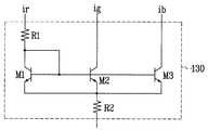
도 3은 본 발명의 제 1 실시 예에 따른 전류 밸런싱부를 나타내는 회로도.3 is a circuit diagram illustrating a current balancing unit according to a first embodiment of the present invention.
도 4는 본 발명의 제 2 실시 예에 따른 전류 밸런싱부를 나타내는 회로도.4 is a circuit diagram illustrating a current balancing unit according to a second embodiment of the present invention.
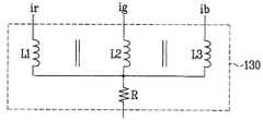
도 5는 본 발명의 제 3 실시 예에 따른 전류 밸런싱부를 나타내는 회로도.5 is a circuit diagram illustrating a current balancing unit according to a third embodiment of the present invention.
도 6은 본 발명의 실시 예에 따른 액정 표시장치를 개략적으로 나타내는 도면.6 is a schematic view of a liquid crystal display according to an exemplary embodiment of the present invention.
< 도면의 주요 부분에 대한 부호설명 ><Explanation of Signs of Major Parts of Drawings>
110 : 발광부 120 : 전원부110: light emitting unit 120: power supply unit
130 : 전류 밸런싱부 140 : 제어부130: current balancing unit 140: control unit
1121 : 적색 발광 다이오드 어레이 1122 : 녹색 발광 다이오드 어레이1121: red light emitting diode array 1122: green light emitting diode array
1123 : 청색 발광 다이오드 어레이1123: blue light emitting diode array
본 발명은 백 라이트 유닛과 이를 이용한 액정 표시장치에 관한 것으로, 특히 백색 광을 발생하기 위한 회로구성을 간소화함과 아울러 화이트 밸런스(White Balance)를 향상시켜 원하는 백색 광을 얻을 수 있도록 한 백 라이트 유닛과 이를 이용한 액정 표시장치에 관한 것이다.BACKGROUND OF THE
통상적으로, 액정 표시장치(Liquid Crystal Display)는 매트릭스 형태로 배열된 다수의 액정셀들과 이들 액정셀들 각각에 공급될 비디오 신호를 절환하기 위한 다수의 제어용 스위치들로 구성된 액정패널에 의해 백 라이트 유닛(Back Light Unit)에서 공급되는 광의 투과량이 조절되어 화면에 원하는 화상을 표시하게 된다.Typically, a liquid crystal display is backlit by a liquid crystal panel composed of a plurality of liquid crystal cells arranged in a matrix and a plurality of control switches for switching a video signal to be supplied to each of the liquid crystal cells. A transmission amount of light supplied from the unit (Back Light Unit) is adjusted to display a desired image on the screen.
백 라이트 유닛은 소형화, 박형화, 경량화의 추세에 있다. 이 추세에 따라 백 라이트 유닛에 사용되는 형광 램프 대신에 소비전력, 무게, 휘도 등에서 유리한 발광 다이오드(Light Emitting Diode)를 이용한 백 라이트 유닛이 제안되었다.The backlight unit is in the trend of miniaturization, thinning and weight reduction. In accordance with this trend, a backlight unit using a light emitting diode (Light Emitting Diode), which is advantageous in terms of power consumption, weight, and brightness, has been proposed instead of the fluorescent lamp used in the backlight unit.
도 1은 종래의 발광 다이오드를 이용한 백 라이트 유닛을 개략적으로 나타내는 도면이다.1 is a view schematically showing a backlight unit using a conventional light emitting diode.
도 1을 참조하면, 종래의 백 라이트 유닛은 적색, 녹색 및 청색 발광 다이오드를 이용하여 백색 광을 발생하는 발광부(10)와, 발광부(10)를 구동시키기 위한 전원 회로부(20)를 포함하여 구성된다.Referring to FIG. 1, a conventional backlight unit includes a
발광부(10)는 직렬 접속된 복수의 적색 발광 다이오드(RLED1 내지 RLEDn)로 구성된 제 1 발광 다이오드 어레이(121), 직렬 접속된 복수의 녹색 발광 다이오 드(GLED1 내지 GLEDn)로 구성된 제 2 발광 다이오드 어레이(122) 및 직렬 접속된 복수의 청색 발광 다이오드(BLED1 내지 BLEDn)로 구성된 제 3 발광 다이오드 어레이(123)를 포함하여 구성된다.The
전원 회로부(20)는 제 1 내지 제 3 발광 다이오드 어레이(121, 122, 123) 각각을 구동시키기 위한 구동전압을 발생하는 제 1 내지 제 3 전원부(221, 222, 223)를 포함하여 구성된다.The power
제 1 전원부(221)는 외부로부터의 전원전압(Vin)을 이용하여 도시하지 않은 제 1 제어부로부터의 제어신호에 따라 제 1 발광 다이오드 어레이(121)의 구동에 필요한 제 1 구동전류(ir)에 대응되는 제 1 구동전압을 발생한다.The first
제 2 전원부(222)는 외부로부터의 전원전압(Vin)을 이용하여 도시하지 않은 제 2 제어부로부터의 제어신호에 따라 제 2 발광 다이오드 어레이(122)의 구동에 필요한 제 2 구동전류(ig)에 대응되는 제 2 구동전압을 발생한다.The second
제 3 전원부(223)는 외부로부터의 전원전압(Vin)을 이용하여 도시하지 않은 제 3 제어부로부터의 제어신호에 따라 제 3 발광 다이오드 어레이(123)의 구동에 필요한 제 3 구동전류(ib)에 대응되는 제 3 구동전압을 발생한다.The third
복수의 적색 발광 다이오드(RLED1 내지 RLEDn)는 제 1 전원부(221)의 출력단과 기저전압원 사이에 직렬 접속되어 제 1 전원부(221)로부터 공급되는 제 1 구동전류(ir)에 의해 구동되어 적색 광을 발생한다.The plurality of red light emitting diodes RLED1 to RLEDn are connected in series between the output terminal of the first
복수의 녹색 발광 다이오드(GLED1 내지 GLEDn)는 제 2 전원부(222)의 출력단과 기저전압원 사이에 직렬 접속되어 제 2 전원부(222)로부터 공급되는 제 2 구동 전류(ig)에 의해 구동되어 녹색 광을 발생한다.The plurality of green light emitting diodes GLED1 to GLEDn are connected in series between the output terminal of the second
복수의 청색 발광 다이오드(BLED1 내지 BLEDn)는 제 3 전원부(223)의 출력단과 기저전압원 사이에 직렬 접속되어 제 3 전원부(223)로부터 공급되는 제 3 구동전류(ib)에 의해 구동되어 적색 광을 발생한다.The plurality of blue light emitting diodes BLED1 to BLEDn are connected in series between the output terminal of the
이와 같은, 종래의 백 라이트 유닛은 적색 발광 다이오드(RLED1 내지 RLEDn) 각각으로부터의 적색 광, 녹색 발광 다이오드(GLED1 내지 GLEDn) 각각으로부터의 녹색 광 및 청색 발광 다이오드(BLED1 내지 BLEDn) 각각으로부터의 청색 광을 혼합하여 백색 광을 발생한다.Such a conventional backlight unit includes red light from each of the red light emitting diodes RLED1 to RLEDn, green light from each of the green light emitting diodes GLED1 to GLEDn, and blue light from each of the blue light emitting diodes BLED1 to BLEDn. To generate white light.
그러나, 종래의 백 라이트 유닛은 제 1 내지 제 3 발광 다이오드 어레이(121, 122, 123)로 구성된 발광부(10)를 구동하여 백색 광을 발생하기 위해서는 3개의 전원부(221, 222, 223) 및 3개의 제어기를 포함해야 하므로 회로구성이 복잡함과 아울러 비용이 증가하는 문제점이 있다.However, the conventional backlight unit includes three
또한, 종래의 백 라이트 유닛은 제 1 내지 제 3 발광 다이오드 어레이(121, 122, 123) 각각이 서로 다른 전원부(221, 222, 223)에 의해 개별적으로 구동되므로 화이트 밸런스를 맞추기 어려우므로 원하는 백색 광을 얻을 수 없는 문제점이 있다.In addition, in the conventional backlight unit, since each of the first to
따라서 상기와 같은 문제점을 해결하기 위하여, 본 발명은 백색 광을 발생하기 위한 회로구성을 간소화함과 아울러 화이트 밸런스(White Balance)를 향상시켜 원하는 백색 광을 얻을 수 있도록 한 백 라이트 유닛과 이를 이용한 액정 표시장치 를 제공하는데 있다.Therefore, in order to solve the above problems, the present invention simplifies the circuit configuration for generating white light and improves the white balance to achieve desired white light and a liquid crystal using the same. To provide a display device.
상기와 같은 기술적 과제를 달성하기 위한 본 발명의 실시 예에 따른 백 라이트 유닛은 적색, 녹색 및 청색 발광 다이오드 어레이를 이용하여 백색 광을 발생하는 발광부와; 상기 적색, 녹색 및 청색 발광 다이오드 어레이에 구동전류를 공급하기 위한 전원부와; 상기 적색, 녹색 및 청색 발광 다이오드 어레이 각각에 흐르는 전류를 조절하여 화이트 밸런스를 맞추기 위한 전류 밸런싱부를 포함하여 구성되는 것을 특징으로 한다.According to an aspect of the present invention, there is provided a backlight unit comprising: a light emitting unit configured to generate white light using red, green, and blue LED arrays; A power supply unit for supplying a driving current to the red, green, and blue LED arrays; And a current balancing unit for adjusting white current by adjusting current flowing through each of the red, green, and blue LED arrays.
상기 전류 밸런싱부는 상기 적색, 녹색 및 청색 발광 다이오드 어레이 중 어느 하나로부터의 전류에 의해 제어되며, 전류 미러(Current Mirror) 형태로 접속된 제 1 내지 제 3 미러 트랜지스터를 포함하여 구성되거나, 상기 적색, 녹색 및 청색 발광 다이오드 어레이에 접속된 마그네틱 소자를 포함하여 구성되는 것을 특징으로 한다.The current balancing unit includes first to third mirror transistors controlled by a current from any one of the red, green, and blue light emitting diode arrays and connected in a current mirror form, or the red, And magnetic elements connected to the green and blue LED arrays.
본 발명의 실시 예에 따른 액정 표시장치는 복수의 게이트 라인과 복수의 데이터 라인에 의해 정의되는 영역마다 형성된 액정셀을 포함하는 화상 표시부와, 외부로부터의 입력 데이터에 대응되는 화상을 상기 화상 표시부에 표시하는 구동 회로부와, 상기 화상 표시부에 광을 조사하는 상기 백 라이트 유닛을 포함하여 구성되는 것을 특징으로 한다.According to an exemplary embodiment of the present invention, a liquid crystal display includes an image display unit including a liquid crystal cell formed for each region defined by a plurality of gate lines and a plurality of data lines, and an image corresponding to input data from outside. And a back light unit for irradiating light to the image display unit.
이하에서, 첨부된 도면 및 실시 예를 통해 본 발명의 실시 예를 구체적으로 살펴보면 다음과 같다.Hereinafter, an embodiment of the present invention will be described in detail with reference to the accompanying drawings and embodiments.
도 2는 본 발명의 실시 예에 따른 백 라이트 유닛을 개략적으로 나타내는 도면이다.2 is a view schematically illustrating a backlight unit according to an exemplary embodiment of the present invention.
도 2를 참조하면, 본 발명의 실시 예에 따른 백 라이트 유닛은 적색, 녹색 및 청색 발광 다이오드 어레이(1121, 1122, 1123)를 이용하여 백색 광을 발생하는 발광부(110)와; 적색, 녹색 및 청색 발광 다이오드 어레이(1121, 1122, 1123)에 구동전류를 공급하기 위한 전원부(120)와; 적색, 녹색 및 청색 발광 다이오드 어레이(1121, 1122, 1123) 각각에 흐르는 전류를 조절하여 화이트 밸런스를 맞추기 위한 전류 밸런싱부(130)와; 전류 밸런싱부(130)로부터의 피드백 신호에 따라 전원부(120)를 제어하는 제어부(140)를 포함하여 구성된다.2, a backlight unit according to an embodiment of the present invention includes a
전원부(120)는 제어부(140)의 제어에 따라 적색, 녹색 및 청색 발광 다이오드 어레이(1121, 1122, 1123)를 구동하기 위한 구동전류를 발생하여 적색, 녹색 및 청색 발광 다이오드 어레이(1121, 1122, 1123)에 공급한다. 이때, 전원부(120)의 출력단은 적색, 녹색 및 청색 발광 다이오드 어레이(1121, 1122, 1123)에 공통으로 접속된다.The
발광부(110)는 전원부(120)와 전류 밸런싱부(130) 사이에 병렬 접속된 적색, 녹색 및 청색 발광 다이오드 어레이(1121, 1122, 1123) 각각에 의해 발생되는 적색 광, 녹색 광 및 청색 광의 혼합에 의해 백색 광을 발생한다.The
적색 발광 다이오드 어레이(1121)는 전원부(120)와 전류 밸런싱부(130) 사이에 직렬 접속된 m개의 적색 발광 다이오드(RLED1 내지 RLEDn)를 포함하여 구성된다. 이때, 직렬 접속된 m개의 적색 발광 다이오드(RLED1 내지 RLEDn) 중 제 1 적 색 발광 다이오드(RLED1)의 캐소드 단자는 전원부(120)의 출력단에 접속되고, 제 m 적색 발광 다이오드(RLEDn)의 애노드 단자는 전류 밸런싱부(130)에 접속된다. 이러한, 적색 발광 다이오드 어레이(1121)는 전원부(120)로부터의 구동전류에 따라 발광하여 적색 광을 발생한다.The red light
녹색 발광 다이오드 어레이(1122)는 전원부(120)와 전류 밸런싱부(130) 사이에 직렬 접속된 m개의 녹색 발광 다이오드(GLED1 내지 GLEDn)를 포함하여 구성된다. 이때, 직렬 접속된 m개의 녹색 발광 다이오드(GLED1 내지 GLEDn) 중 제 1 녹색 발광 다이오드(GLED1)의 캐소드 단자는 전원부(120)의 출력단에 접속되고, 제 m 녹색 발광 다이오드(GLEDn)의 애노드 단자는 전류 밸런싱부(130)에 접속된다. 이러한, 녹색 발광 다이오드 어레이(1122)는 전원부(120)로부터의 구동전류에 따라 발광하여 녹색 광을 발생한다.The green light
청색 발광 다이오드 어레이(1123)는 전원부(120)와 전류 밸런싱부(130) 사이에 직렬 접속된 m개의 청색 발광 다이오드(BLED1 내지 BLEDn)를 포함하여 구성된다. 이때, 직렬 접속된 m개의 청색 발광 다이오드(BLED1 내지 BLEDn) 중 제 1 청색 발광 다이오드(BLED1)의 캐소드 단자는 전원부(120)의 출력단에 접속되고, 제 m 청색 발광 다이오드(BLEDn)의 애노드 단자는 전류 밸런싱부(130)에 접속된다. 이러한, 청색 발광 다이오드 어레이(1123)는 전원부(120)로부터의 구동전류에 따라 발광하여 청색 광을 발생한다.The blue light
전류 밸런싱부(130)는 각 발광 다이오드 어레이(1121, 1122, 1123)와 기저전압원 사이에 접속된다. 이러한, 전류 밸런싱부(130)는 발광부(110)의 화이트 밸런 스를 맞추어 발광부(110)에서 원하는 백색 광을 발생되도록 적색, 녹색 및 청색 발광 다이오드 어레이(1121, 1122, 1123) 각각에 흐르는 전류(ir, ig, ib)를 밸런싱한다.The
제어부(140)는 피드백 라인(FBL)을 통해 전류 밸런싱부(130)로부터 기저전압원으로 흐르는 전류를 피드백하여 전원부(120)를 제어하기 위한 제어신호(CS)를 생성함으로써 전원부(120)로부터 각 발광 다이오드 어레이(1121, 1122, 1123)에 흐르는 전류를 제어한다. 이에 따라, 전원부(120)는 입력전원(Vin)을 이용하여 제어부(140)로부터의 제어신호(CS)에 따라 구동전류를 발생하여 각 발광 다이오드 어레이(1121, 1122, 1123)에 공급한다.The
이와 같은, 본 발명의 실시 예에 따른 백 라이트 유닛은 전류 밸런싱부(130)를 이용하여 각 발광 다이오드 어레이(1121, 1122, 1123)에 흐르는 전류를 밸런싱함으로써 발광부(110)의 화이트 밸런스를 맞추어 원하는 화이트 포인트(White Point)를 가지는 백색 광을 발생할 수 있다.As described above, the backlight unit according to the embodiment of the present invention adjusts the white balance of the
또한, 본 발명의 실시 예에 따른 백 라이트 유닛은 전류 밸런싱부(130)를 이용하여 하나의 전원부(120) 및 하나의 제어부(140)로 적색, 녹색 및 청색 발광 다이오드 어레이(1121, 1122, 1123)를 구동함으로써 회로구성을 간소화할 수 있다.In addition, the backlight unit according to the exemplary embodiment of the present invention uses the
도 3은 본 발명의 제 1 실시 예에 따른 전류 밸런싱부(130)를 나타내는 회로도이다.3 is a circuit diagram illustrating the
도 3을 도 2와 결부하면, 본 발명의 제 1 실시 예에 따른 전류 밸런싱부(130)는 적색 발광 다이오드 어레이(1121)에 흐르는 전류(ir)에 의해 제어되며, 전류 미러(Current Mirror) 형태로 접속된 제 1 내지 제 3 미러 트랜지스터(M1, M2, M3)를 포함하여 구성된다. 여기서, 제 1 내지 제 3 미러 트랜지스터(M1, M2, M3) 각각은 바이폴라 트랜지스터이다.Referring to FIG. 3 and FIG. 2, the
제 1 미러 트랜지스터(M1)의 베이스(Base) 단자 및 컬렉터(Collector) 단자는 제 1 저항(R1)을 통해 적색 발광 다이오드 어레이(1121)의 끝단에 공통으로 접속되고, 이미터(Emitter) 단자는 제 2 저항(R2)을 통해 기저전압원에 접속된다.The base terminal and the collector terminal of the first mirror transistor M1 are commonly connected to the ends of the red light emitting
제 2 미러 트랜지스터(M2)의 베이스 단자는 제 1 미러 트랜지스터(M1)의 베이스 단자에 접속되고, 컬렉터 단자는 녹색 발광 다이오드 어레이(1122)의 끝단에 접속되고, 이미터 단자는 제 2 저항(R2)을 통해 기저전압원에 접속된다.The base terminal of the second mirror transistor M2 is connected to the base terminal of the first mirror transistor M1, the collector terminal is connected to the end of the green light emitting
제 3 미러 트랜지스터(M3)의 베이스 단자는 제 1 미러 트랜지스터(M1)의 베이스 단자에 접속되고, 컬렉터 단자는 청색 발광 다이오드 어레이(1123)의 끝단에 접속되고, 이미터 단자는 제 2 저항(R2)을 통해 기저전압원에 접속된다.The base terminal of the third mirror transistor M3 is connected to the base terminal of the first mirror transistor M1, the collector terminal is connected to the end of the blue light emitting
이와 같은, 전류 밸런싱부(130)는 제 1 내지 제 3 미러 트랜지스터(M1, M2, M3)를 이용하여 각 발광 다이오드 어레이(1121, 1122, 1123)에 흐르는 전류(ir, ig, ib)를 일정하게 제어함과 아울러 화이트 밸런스를 맞추도록 각 발광 다이오드 어레이(1121, 1122, 1123)에 흐르는 전류(ir, ig, ib)를 밸런싱한다.As such, the
일반적으로 전류 미러 형태로 접속된 트랜지스터에 흐르는 전류는 아래의 수학식 1과 같이 트랜지스터의 전류 증폭률(β)에 영향을 받음을 알 수 있다.In general, it can be seen that the current flowing through a transistor connected in the form of a current mirror is affected by the current amplification factor β of the transistor as shown in

트랜지스터의 전류 증폭률(β)은 아래의 수학식 2와 같이 나타낼 수 있다.The current amplification factor β of the transistor can be expressed by Equation 2 below.

수학식 2에 있어서, Dn은 베이스에서의 전자 확산율, Dp는 이미터에서의 정공(Hole) 확산율, ND는 이미터의 도핑농도, NA는 베이스의 도핑농도, Lp는 이미터에서의 정공 확산 거리, W는 유효한 베이스의 폭(Width), τb는 베이스에서의 소수 캐리어 생존 시간을 나타낸다.In Equation 2, Dn is the electron diffusion rate in the base, Dp is the hole diffusion rate in the emitter, ND is the doping concentration of the emitter, NA is the base doping concentration, Lp is the hole in the emitter The spreading distance, W, is the effective width of the base, τb is the minority carrier survival time at the base.
이와 같은, 수학식 1 및 2에서와 같이 제 1 내지 제 3 미러 트랜지스터(M1, M2, M3)에 의해 각 발광 다이오드 어레이(1121, 1122, 1123)에 흐르는 전류 편차에 영향을 미치는 주요 요인은 전류 증폭률(β1, β2, β3) 및 도핑농도(NA/ND)임을 알 수 있다.As shown in
따라서, 전류 밸런싱부(130)는 제 1 내지 제 3 미러 트랜지스터(M1, M2, M3)의 전류 증폭률(β1, β2, β3) 및 도핑농도(NA/ND)를 이용하여각 발광 다이오드 어레이(1121, 1122, 1123)에 의한 화이트 밸런스를 맞출 수 있다.Accordingly, the
예를 들어, 발광부(110)에서 발생되는 백색 광의 화이트 밸런스를 맞추기 위하여 적색 발광 다이오드 어레이(1121)에 흐르는 적색 구동전류(ir), 녹색 발광 다이오드 어레이(1122)에 흐르는 녹색 구동전류(ig) 및 청색 발광 다이오드 어레이(1123)에 흐르는 청색 구동전류(ib)의 비(ir:ig:ib)가 '1:2:2'일 경우, 각 미러 트랜지스터(M1, M2, M3)의 베이스의 폭(W)이 '1:2:2'로 형성되어 각 미러 트랜지스터(M1, M2, M3)의 전류 증폭률(β1, β2, β3)은 '1:2:2'로 설정된다. 이에 따라, 전류 밸런싱부(130)는 원하는 화이트 밸런스를 맞추도록 각 미러 트랜지스터(M1, M2, M3)의 전류 증폭률(β1, β2, β3)를 설정함으로써 화이트 밸런스를 맞출 수 있도록 각 미러 트랜지스터(M1, M2, M3)에 흐르는 전류량을 설정한다. 이때, 각 미러 트랜지스터(M1, M2, M3)의 도핑농도(NA/ND)는 동일하다고 가정한다.For example, in order to balance the white balance of the white light generated by the
한편, 제 1 내지 제 3 미러 트랜지스터(M1, M2, M3)의 전류 증폭률(β1, β2, β3)은 실험적으로 설정될 수 있으며, 제 1 미러 트랜지스터(M1)의 전류 증폭률(β1)은 제 2 및 제 3 미러 트랜지스터(M2, M3)의 전류 증폭률(β2, β3)보다 작으며, 제 2 미러 트랜지스터(M2)의 전류 증폭률(β2)은 제 3 미러 트랜지스터(M3)의 전류 증폭률(β3)과 같거나 작을 수 있다.Meanwhile, the current amplification ratios β1, β2, and β3 of the first to third mirror transistors M1, M2, and M3 may be experimentally set, and the current amplification ratio β1 of the first mirror transistor M1 may be set to the second. And the current amplification ratio β2 of the second mirror transistor M2 is smaller than the current amplification ratio β2, β3 of the third mirror transistors M2 and M3. It can be the same or less.
도 4는 본 발명의 제 2 실시 예에 따른 전류 밸런싱부(130)를 나타내는 회로도이다.4 is a circuit diagram illustrating the
도 4를 도 2와 결부하면, 본 발명의 제 2 실시 예에 따른 전류 밸런싱부(130)는 적색 발광 다이오드 어레이(1121)에 흐르는 전류(ir)에 의해 제어되며, 전류 미러 형태로 접속된 제 1 내지 제 3 미러 트랜지스터(Q1, Q2, Q3)를 포함하여 구성된다. 여기서, 제 1 내지 제 3 미러 트랜지스터(Q1, Q2, Q3) 각각은 전계효과 트랜지스터이다.Referring to FIG. 4 and FIG. 2, the
제 1 미러 트랜지스터(Q1)의 게이트 단자 및 소스 단자는 저항(R)을 통해 적색 발광 다이오드 어레이(1121)의 끝단에 공통으로 접속되고, 드레인 단자는 기저전압원에 접속된다.The gate terminal and the source terminal of the first mirror transistor Q1 are commonly connected to the ends of the red light emitting
제 2 미러 트랜지스터(Q2)의 게이트 단자는 제 1 미러 트랜지스터(Q1)의 게이트 단자에 접속되고, 소스 단자는 녹색 발광 다이오드 어레이(1122)의 끝단에 접속되고, 드레인 단자는 기저전압원에 접속된다.The gate terminal of the second mirror transistor Q2 is connected to the gate terminal of the first mirror transistor Q1, the source terminal is connected to the end of the green light emitting
제 3 미러 트랜지스터(Q3)의 게이트 단자는 제 1 미러 트랜지스터(Q1)의 게이트 단자에 접속되고, 소스 단자는 청색 발광 다이오드 어레이(1123)의 끝단에 접속되고, 드레인 단자는 기저전압원에 접속된다.The gate terminal of the third mirror transistor Q3 is connected to the gate terminal of the first mirror transistor Q1, the source terminal is connected to the end of the blue light emitting
이와 같은, 전류 밸런싱부(130)는 제 1 내지 제 3 미러 트랜지스터(Q1, Q2, Q3)를 이용하여 각 발광 다이오드 어레이(1121, 1122, 1123)에 흐르는 전류(ir, ig, ib)를 일정하게 제어함과 아울러 화이트 밸런스를 맞추도록 각 발광 다이오드 어레이(1121, 1122, 1123)에 흐르는 전류(ir, ig, ib)를 밸런싱한다.As such, the
이를 위해, 제 1 내지 제 3 미러 트랜지스터(M1, M2, M3)의 채널 폭(W) 및 길이(L)는 원하는 화이트 밸런스를 맞추기 위하여 실험적으로 설정될 수 있으며, 제 1 미러 트랜지스터(M1)의 채널 폭(W) 및 길이(L)는 제 2 및 제 3 미러 트랜지스터(M2, M3)의 채널 폭(W) 및 길이(L)보다 작으며, 제 2 미러 트랜지스터(M2)의 채 널 폭(W) 및 길이(L)는 제 3 미러 트랜지스터(M3)의 채널 폭(W) 및 길이(L)와 같거나 작을 수 있다.To this end, the channel width W and the length L of the first to third mirror transistors M1, M2, and M3 may be experimentally set to achieve a desired white balance. The channel width W and the length L are smaller than the channel width W and the length L of the second and third mirror transistors M2 and M3, and the channel width W of the second mirror transistor M2 is determined. W) and the length L may be equal to or smaller than the channel width W and the length L of the third mirror transistor M3.
도 5는 본 발명의 제 3 실시 예에 따른 전류 밸런싱부(130)를 나타내는 회로도이다.5 is a circuit diagram illustrating a
도 5를 참조하면, 본 발명의 제 3 실시 예에 따른 전류 밸런싱부(130)는 적색, 녹색 및 청색 발광 다이오드 어레이(1121, 1122, 1123)에 접속되어 적색, 녹색 및 청색 발광 다이오드 어레이(1121, 1122, 1123)에 걸리는 임피던스(Impedance) 편차를 보상하는 마그네틱 소자를 포함하여 구성된다.Referring to FIG. 5, the
마그네틱 소자는 커플링 인덕터 또는 다채널 트랜스포머로써 적색, 녹색 및 청색 발광 다이오드 어레이(1121, 1122, 1123) 각각에 접속됨과 아울러 저항(R)을 통해 기저전압원에 접속되는 제 1 내지 제 3 권선(L1, L2, L3)을 포함하여 구성된다.The magnetic element is a coupling inductor or a multi-channel transformer connected to each of the red, green, and blue light emitting
제 1 내지 제 3 권선(L1, L2, L3)은 적색, 녹색 및 청색 발광 다이오드 어레이(1121, 1122, 1123)에 걸리는 임피던스 편차를 보상 및 원하는 화이트 밸런스를 맞추기 위하여 서로 동일한 권선비를 가지거나 서로 다른 권선비를 가질 수 있다.The first to third windings L1, L2, and L3 have the same turns ratio or different from each other in order to compensate for the impedance variation across the red, green, and blue light emitting
이와 같은, 본 발명의 제 3 실시 예에 따른 전류 밸런싱부(130)는 제 1 내지 제 3 권선(L1, L2, L3)의 권선비를 이용하여 적색, 녹색 및 청색 발광 다이오드 어레이(1121, 1122, 1123)에 걸리는 임피던스 편차를 보상함과 아울러 원하는 화이트 밸런스를 맞출 수 있다.As such, the
도 6은 본 발명의 실시 예에 따른 액정 표시장치를 개략적으로 나타내는 도 면이다.6 is a diagram schematically illustrating a liquid crystal display according to an exemplary embodiment of the present invention.
도 6을 참조하면, 본 발명의 실시 예에 따른 액정 표시장치는 n개의 게이트 라인(GL1 내지 GLn)과 m개의 데이터 라인(DL1 내지 DLm)에 의해 정의되는 영역마다 형성된 액정셀을 포함하는 화상 표시부(300)와, 외부로부터의 입력 데이터(Data)에 대응되는 화상을 화상 표시부(300)에 표시하기 위한 구동 회로부(310)와, 화상 표시부(300)에 광을 조사하기 위한 백 라이트 유닛(320)을 포함하여 구성된다.Referring to FIG. 6, a liquid crystal display according to an exemplary embodiment of the present invention includes an image display unit including a liquid crystal cell formed for each region defined by n gate lines GL1 to GLn and m data lines DL1 to DLm. 300, a driving
화상 표시부(300)는 n개의 게이트 라인(GL1 내지 GLn)과 m개의 데이터 라인(DL1 내지 DLm)에 의해 정의되는 영역에 형성된 박막 트랜지스터(TFT)와, 박막 트랜지스터(TFT)에 접속되는 액정셀들을 구비한다. 박막 트랜지스터(TFT)는 게이트 라인(GL1 내지 GLn)으로부터의 스캔펄스에 응답하여 데이터 라인(DL1 내지 DLm)으로부터의 데이터 신호를 액정셀로 공급한다. 액정셀은 액정을 사이에 두고 대면하는 공통전극과 박막 트랜지스터(TFT)에 접속된 서브 픽셀전극으로 구성되므로 등가적으로 액정 커패시터(Clc)로 표시될 수 있다. 또한, 액정셀은 액정 커패시터(Clc)에 충전된 데이터 신호를 다음 데이터 신호가 충전될 때까지 유지시키기 위한 스토리지 커패시터(Cst)를 포함한다.The
구동 회로부(310)는 게이트 제어신호(GCS)에 따라 스캔펄스를 생성하여 게이트 라인들(GL1 내지 GLn)에 순차적으로 공급하는 게이트 구동부(312)와; 데이터 제어신호(DCS)에 따라 입력 데이터(Data)를 화상신호로 변환하여 스캔펄스에 동기되도록 해당 데이터 라인(DL1 내지 DLm)에 공급하는 데이터 구동부(314)와; 입력 데이터(Data)를 정렬하여 데이터 구동부(314)에 공급하고 게이트 및 데이터 구동 부(312, 314) 각각을 제어하는 타이밍 컨트롤러(316)를 포함하여 구성된다.The driving
게이트 구동부(312)는 타이밍 컨트롤러(316)로부터의 게이트 제어신호(GCS)에 따라 스캔펄스 즉, 게이트 하이펄스를 순차적으로 발생하여 게이트 라인들(GL1 내지 GLn)에 순차적으로 공급한다. 이 스캔펄스에 응답하여 박막 트랜지스터(TFT)는 턴-온된다.The
데이터 구동부(314)는 타이밍 컨트롤러(316)로부터 공급되는 데이터 제어신호(DCS)에 따라 타이밍 컨트롤러(316)로부터 공급되는 데이터(R,G,B)를 아날로그 신호인 화상신호로 변환하여 게이트 라인들(GL1 내지 GLn)에 스캔펄스가 공급되는 1수평 주기마다 1수평 라인분의 화상신호를 데이터 라인들(DL1 내지 DLm)로 공급한다. 이때, 데이터 구동부(314)는 극성 제어신호에 응답하여 데이터 라인들(DL1 내지 DLm)에 공급되는 화상신호의 극성을 반전시키게 된다.The
타이밍 컨트롤러(316)는 외부로부터의 입력 데이터(Data)를 화상 표시부(300)의 구동에 알맞도록 정렬하여 데이터 구동부(314)에 공급한다.The
또한, 타이밍 컨트롤러(316)는 외부로부터 입력되는 동기신호, 즉 도트클럭(DCLK), 데이터 인에이블 신호(DE), 수평 및 수직 동기신호(Hsync, Vsync)를 이용하여 게이트 구동부(312)의 구동 타이밍을 제어하기 위한 게이트 제어신호(GCS)와 데이터 구동부(314)의 구동 타이밍을 제어하기 위한 데이터 제어신호(DCS)를 생성한다.In addition, the
백 라이트 유닛(320)은 적어도 하나의 적색 발광 다이오드 어레이로부터의 적색 광, 적어도 하나의 녹색 발광 다이오드 어레이로부터의 녹색 광 및 적어도 하 나의 청색 발광 다이오드 어레이로부터의 청색 광을 혼합하여 백색 광을 발생하고, 발생된 백색 광을 화상 표시부(300)에 조사한다.The
이를 위해 백 라이트 유닛(320)은 도 2에 도시된 본 발명의 실시 예에 따른 백 라이트 유닛과 동일한 구성을 갖는다. 또한, 백 라이트 유닛(320)은 도 3 내지 제 5에 도시된 본 발명의 제 1 내지 제 3 실시 예에 따른 전류 밸런싱부를 포함하여 구성된다. 이러한, 백 라이트 유닛(320)에 대한 설명은 상술한 도 2 내지 도 5에 대한 설명으로 대신하기로 한다.To this end, the
이와 같은, 본 발명의 실시 예에 따른 액정 표시장치는 화상 표시부(300)에 공급되는 화상신호에 따라 백 라이트 유닛(320)으로부터 조사되는 광투과율을 조절하여 원하는 화상을 화상 표시부(300)에 표시한다.As described above, the liquid crystal display according to the exemplary embodiment of the present invention adjusts the light transmittance emitted from the
따라서, 본 발명의 실시 예에 따른 액정 표시장치는 전류 밸런싱부에 의해 원하는 화이트 밸런스를 가지는 백색 광을 이용하여 원하는 화상을 표시함으로써 화질을 향상시킬 수 있다.Therefore, the liquid crystal display according to the exemplary embodiment of the present invention may improve image quality by displaying a desired image by using white light having a desired white balance by the current balancing unit.
한편, 이상에서 설명한 본 발명은 상술한 실시 예 및 첨부된 도면에 한정되는 것이 아니고, 본 발명의 기술적 사상을 벗어나지 않는 범위내에서 여러 가지 치환, 변형 및 변경이 가능하다는 것이 본 발명이 속하는 기술분야에서 종래의 지식을 가진 자에게 있어 명백할 것이다.On the other hand, the present invention described above is not limited to the above-described embodiment and the accompanying drawings, it is possible that various substitutions, modifications and changes within the scope without departing from the technical spirit of the present invention It will be apparent to those skilled in the art.
상기와 같은 본 발명의 실시 예에 따른 백 라이트 유닛과 이를 이용한 액정 표시장치는 전류 밸런싱부를 이용하여 적색, 녹색 및 청색 발광 다이오드 어레이에 흐르는 전류를 밸런싱함으로써 화이트 밸런스를 맞추어 원하는 화이트 포인트를 가지는 백색 광을 발생할 수 있다.The backlight unit and the liquid crystal display using the same according to the embodiment of the present invention, the white light having a desired white point by adjusting the white balance by balancing the current flowing through the red, green and blue LED array using the current balancing unit May occur.
또한, 본 발명은 전류 밸런싱부를 이용하여 하나의 전원부 및 하나의 제어부로 적색, 녹색 및 청색 발광 다이오드 어레이를 구동함으로써 회로구성을 간소화할 수 있다.In addition, the present invention can simplify the circuit configuration by driving the red, green and blue LED array with one power supply and one control unit using the current balancing unit.
Claims (15)
Translated fromKoreanPriority Applications (2)
| Application Number | Priority Date | Filing Date | Title |
|---|---|---|---|
| KR1020060087848AKR101255268B1 (en) | 2006-09-12 | 2006-09-12 | Back light unit and liquid crystal display device using the same |
| US11/895,572US20080061716A1 (en) | 2006-09-12 | 2007-08-24 | Backlight unit and crystal display device using the same |
Applications Claiming Priority (1)
| Application Number | Priority Date | Filing Date | Title |
|---|---|---|---|
| KR1020060087848AKR101255268B1 (en) | 2006-09-12 | 2006-09-12 | Back light unit and liquid crystal display device using the same |
Publications (2)
| Publication Number | Publication Date |
|---|---|
| KR20080023810A KR20080023810A (en) | 2008-03-17 |
| KR101255268B1true KR101255268B1 (en) | 2013-04-15 |
Family
ID=39168870
Family Applications (1)
| Application Number | Title | Priority Date | Filing Date |
|---|---|---|---|
| KR1020060087848AExpired - Fee RelatedKR101255268B1 (en) | 2006-09-12 | 2006-09-12 | Back light unit and liquid crystal display device using the same |
Country Status (2)
| Country | Link |
|---|---|
| US (1) | US20080061716A1 (en) |
| KR (1) | KR101255268B1 (en) |
Families Citing this family (24)
| Publication number | Priority date | Publication date | Assignee | Title |
|---|---|---|---|---|
| TW200935713A (en)* | 2008-02-01 | 2009-08-16 | Delta Electronics Inc | Current balancing power supply circuit for multiple groups of DC loads |
| WO2009124432A1 (en)* | 2008-04-11 | 2009-10-15 | 深圳市联德合微电子有限公司 | An led constant current driving circuit |
| TWI391028B (en)* | 2008-04-18 | 2013-03-21 | Novatek Microelectronics Corp | Light emitting diode module |
| EP2306070A4 (en)* | 2008-07-29 | 2013-07-03 | Sharp Kk | LIGHTING APPARATUS, DISPLAY APPARATUS AND TELEVISION RECEIVER |
| CN101794559B (en)* | 2009-02-03 | 2013-03-20 | 乐金显示有限公司 | Backlight assembly of liquid crystal display device |
| KR20100113787A (en)* | 2009-04-14 | 2010-10-22 | 삼성전자주식회사 | Light source module, back light unit and display apparatus |
| US20100295471A1 (en)* | 2009-05-25 | 2010-11-25 | Sanken Electric Co., Ltd. | Current balancing apparatus |
| TWI429319B (en)* | 2009-05-29 | 2014-03-01 | Lg Innotek Co Ltd | Led driver |
| KR101029546B1 (en)* | 2009-05-29 | 2011-04-15 | 한양대학교 산학협력단 | Light emitting device that can control color temperature |
| KR101033732B1 (en)* | 2009-05-29 | 2011-05-09 | 엘지이노텍 주식회사 | LED Driver |
| KR101677730B1 (en)* | 2009-08-14 | 2016-11-30 | 페어차일드코리아반도체 주식회사 | LED light emitting device |
| US8525774B2 (en)* | 2009-10-28 | 2013-09-03 | Top Victory Investments Ltd. | Light-emitting diode (LED) driving circuit |
| KR101665306B1 (en)* | 2009-12-21 | 2016-10-12 | 엘지디스플레이 주식회사 | Apparatus and method for driving of light emitting diode, and liquid crystal display device using the same |
| KR101688560B1 (en)* | 2009-12-22 | 2016-12-21 | 엘지디스플레이 주식회사 | Back light unit and liquid crystal display device using the same |
| CN102118903A (en)* | 2009-12-30 | 2011-07-06 | 富准精密工业(深圳)有限公司 | Drive circuit for LED (light-emitting diode) light fixture |
| US8350498B2 (en) | 2010-04-28 | 2013-01-08 | National Semiconductor Corporation | Dynamic current equalization for light emitting diode (LED) and other applications |
| WO2012012195A2 (en)* | 2010-07-19 | 2012-01-26 | Microsemi Corporation | Led string driver arrangement with non-dissipative current balancer |
| US20120218283A1 (en)* | 2011-02-28 | 2012-08-30 | Spatial Photonics, Inc. | Method for Obtaining Brighter Images from an LED Projector |
| KR20120114023A (en) | 2011-04-06 | 2012-10-16 | 삼성디스플레이 주식회사 | Back light unit and display device including the same |
| US8754581B2 (en) | 2011-05-03 | 2014-06-17 | Microsemi Corporation | High efficiency LED driving method for odd number of LED strings |
| CN103477712B (en) | 2011-05-03 | 2015-04-08 | 美高森美公司 | High efficiency LED driving method |
| JP5984501B2 (en)* | 2012-05-15 | 2016-09-06 | 三菱電機株式会社 | Projection display |
| KR20180019327A (en) | 2016-08-16 | 2018-02-26 | 삼성전자주식회사 | Led driving apparatus, display apparatus and method for driving led |
| KR20190108127A (en)* | 2017-01-27 | 2019-09-23 | 로히니, 엘엘씨. | Apparatus and Method for Distributed Control of Semiconductor Device Arrays |
Citations (4)
| Publication number | Priority date | Publication date | Assignee | Title |
|---|---|---|---|---|
| KR20020084125A (en)* | 2000-12-12 | 2002-11-04 | 코닌클리즈케 필립스 일렉트로닉스 엔.브이. | Control and drive circuit arrangement |
| KR20040091415A (en)* | 2003-04-21 | 2004-10-28 | 삼성전자주식회사 | Power Supply, Liquid Crystal Display Device And Driving Method For The Same |
| JP2005310996A (en) | 2004-04-20 | 2005-11-04 | Sony Corp | Fixed current driving device, back light optical source equipment, and color liquid crystal display device |
| KR20060012991A (en)* | 2004-08-05 | 2006-02-09 | 삼성에스디아이 주식회사 | LCD and its driving method |
Family Cites Families (3)
| Publication number | Priority date | Publication date | Assignee | Title |
|---|---|---|---|---|
| JP2007005615A (en)* | 2005-06-24 | 2007-01-11 | Olympus Corp | Light source and projection display |
| JP4544068B2 (en)* | 2005-07-14 | 2010-09-15 | ソニー株式会社 | Light emitting diode element drive circuit, light source device, display device |
| TWI298599B (en)* | 2006-03-03 | 2008-07-01 | Au Optronics Corp | Organic light emitting display, panel and driving device thereof |
- 2006
- 2006-09-12KRKR1020060087848Apatent/KR101255268B1/ennot_activeExpired - Fee Related
- 2007
- 2007-08-24USUS11/895,572patent/US20080061716A1/ennot_activeAbandoned
Patent Citations (4)
| Publication number | Priority date | Publication date | Assignee | Title |
|---|---|---|---|---|
| KR20020084125A (en)* | 2000-12-12 | 2002-11-04 | 코닌클리즈케 필립스 일렉트로닉스 엔.브이. | Control and drive circuit arrangement |
| KR20040091415A (en)* | 2003-04-21 | 2004-10-28 | 삼성전자주식회사 | Power Supply, Liquid Crystal Display Device And Driving Method For The Same |
| JP2005310996A (en) | 2004-04-20 | 2005-11-04 | Sony Corp | Fixed current driving device, back light optical source equipment, and color liquid crystal display device |
| KR20060012991A (en)* | 2004-08-05 | 2006-02-09 | 삼성에스디아이 주식회사 | LCD and its driving method |
Also Published As
| Publication number | Publication date |
|---|---|
| KR20080023810A (en) | 2008-03-17 |
| US20080061716A1 (en) | 2008-03-13 |
Similar Documents
| Publication | Publication Date | Title |
|---|---|---|
| KR101255268B1 (en) | Back light unit and liquid crystal display device using the same | |
| KR101255276B1 (en) | Back light unit and liquid crystal display device using the same | |
| CN110718195B (en) | Light emitting device, display device, and LED display device | |
| US7728810B2 (en) | Display device and method for driving the same | |
| US8847876B2 (en) | Device and method for driving liquid crystal display device | |
| US7936324B2 (en) | Liquid crystal display device and driving method thereof | |
| KR20070090566A (en) | Driving device of backlight assembly of liquid crystal display device | |
| KR101229773B1 (en) | Lamp driving apparatus of liquid crystal display device | |
| KR20110072692A (en) | Driving device of LED array and liquid crystal display including the same | |
| KR102091197B1 (en) | Apparatus for driving a light emitting diode array and liquid crystal display device using the same | |
| CN101430456B (en) | Backlight unit and LCD device using the same | |
| US20050264504A1 (en) | Liquid crystal display and a driving method thereof | |
| US8400378B2 (en) | Electro-luminescence pixel, panel with the pixel, and device and method for driving the panel | |
| KR20130036881A (en) | Organic light emitting diode display device and method for driving the same | |
| KR20120061542A (en) | Light emitting diode backlight and liquid crystal display device including the same | |
| KR20090068591A (en) | Back light unit, liquid crystal display using same and driving method thereof | |
| KR102135912B1 (en) | Back light unit and liquid crystal display device using the same and driving method thereof | |
| KR20120019741A (en) | Liquid crystal display device and method of driving the same | |
| KR101633098B1 (en) | Backlight unit | |
| KR101869823B1 (en) | Liquid crystal display device and driving method the same | |
| KR20090054581A (en) | LED driving circuit, backlight unit and liquid crystal display using the same | |
| KR100627311B1 (en) | Liquid crystal display | |
| KR20080050877A (en) | LCD and its driving method | |
| KR100658674B1 (en) | Backlight driving circuit | |
| US20100045710A1 (en) | Backlight apparatus and a liquid crystal display including the same |
Legal Events
| Date | Code | Title | Description |
|---|---|---|---|
| PA0109 | Patent application | St.27 status event code:A-0-1-A10-A12-nap-PA0109 | |
| PG1501 | Laying open of application | St.27 status event code:A-1-1-Q10-Q12-nap-PG1501 | |
| PN2301 | Change of applicant | St.27 status event code:A-3-3-R10-R13-asn-PN2301 St.27 status event code:A-3-3-R10-R11-asn-PN2301 | |
| R18-X000 | Changes to party contact information recorded | St.27 status event code:A-3-3-R10-R18-oth-X000 | |
| A201 | Request for examination | ||
| PA0201 | Request for examination | St.27 status event code:A-1-2-D10-D11-exm-PA0201 | |
| R18-X000 | Changes to party contact information recorded | St.27 status event code:A-3-3-R10-R18-oth-X000 | |
| R18-X000 | Changes to party contact information recorded | St.27 status event code:A-3-3-R10-R18-oth-X000 | |
| E902 | Notification of reason for refusal | ||
| PE0902 | Notice of grounds for rejection | St.27 status event code:A-1-2-D10-D21-exm-PE0902 | |
| E13-X000 | Pre-grant limitation requested | St.27 status event code:A-2-3-E10-E13-lim-X000 | |
| P11-X000 | Amendment of application requested | St.27 status event code:A-2-2-P10-P11-nap-X000 | |
| P13-X000 | Application amended | St.27 status event code:A-2-2-P10-P13-nap-X000 | |
| E701 | Decision to grant or registration of patent right | ||
| PE0701 | Decision of registration | St.27 status event code:A-1-2-D10-D22-exm-PE0701 | |
| GRNT | Written decision to grant | ||
| PR0701 | Registration of establishment | St.27 status event code:A-2-4-F10-F11-exm-PR0701 | |
| PR1002 | Payment of registration fee | St.27 status event code:A-2-2-U10-U11-oth-PR1002 Fee payment year number:1 | |
| PG1601 | Publication of registration | St.27 status event code:A-4-4-Q10-Q13-nap-PG1601 | |
| FPAY | Annual fee payment | Payment date:20160329 Year of fee payment:4 | |
| PR1001 | Payment of annual fee | St.27 status event code:A-4-4-U10-U11-oth-PR1001 Fee payment year number:4 | |
| FPAY | Annual fee payment | Payment date:20170320 Year of fee payment:5 | |
| PR1001 | Payment of annual fee | St.27 status event code:A-4-4-U10-U11-oth-PR1001 Fee payment year number:5 | |
| PR1001 | Payment of annual fee | St.27 status event code:A-4-4-U10-U11-oth-PR1001 Fee payment year number:6 | |
| FPAY | Annual fee payment | Payment date:20190318 Year of fee payment:7 | |
| PR1001 | Payment of annual fee | St.27 status event code:A-4-4-U10-U11-oth-PR1001 Fee payment year number:7 | |
| PR1001 | Payment of annual fee | St.27 status event code:A-4-4-U10-U11-oth-PR1001 Fee payment year number:8 | |
| PR1001 | Payment of annual fee | St.27 status event code:A-4-4-U10-U11-oth-PR1001 Fee payment year number:9 | |
| PR1001 | Payment of annual fee | St.27 status event code:A-4-4-U10-U11-oth-PR1001 Fee payment year number:10 | |
| PC1903 | Unpaid annual fee | St.27 status event code:A-4-4-U10-U13-oth-PC1903 Not in force date:20230410 Payment event data comment text:Termination Category : DEFAULT_OF_REGISTRATION_FEE | |
| PC1903 | Unpaid annual fee | St.27 status event code:N-4-6-H10-H13-oth-PC1903 Ip right cessation event data comment text:Termination Category : DEFAULT_OF_REGISTRATION_FEE Not in force date:20230410 |