KR101254695B1 - Liquid crystal display panel with a built-in touch screen and liquid crystal display having the same - Google Patents
Liquid crystal display panel with a built-in touch screen and liquid crystal display having the sameDownload PDFInfo
- Publication number
- KR101254695B1 KR101254695B1KR1020060041786AKR20060041786AKR101254695B1KR 101254695 B1KR101254695 B1KR 101254695B1KR 1020060041786 AKR1020060041786 AKR 1020060041786AKR 20060041786 AKR20060041786 AKR 20060041786AKR 101254695 B1KR101254695 B1KR 101254695B1
- Authority
- KR
- South Korea
- Prior art keywords
- substrate
- liquid crystal
- crystal display
- display panel
- touch screen
- Prior art date
- Legal status (The legal status is an assumption and is not a legal conclusion. Google has not performed a legal analysis and makes no representation as to the accuracy of the status listed.)
- Expired - Fee Related
Links
Images


Classifications
- G—PHYSICS
- G06—COMPUTING OR CALCULATING; COUNTING
- G06F—ELECTRIC DIGITAL DATA PROCESSING
- G06F3/00—Input arrangements for transferring data to be processed into a form capable of being handled by the computer; Output arrangements for transferring data from processing unit to output unit, e.g. interface arrangements
- G06F3/01—Input arrangements or combined input and output arrangements for interaction between user and computer
- G06F3/03—Arrangements for converting the position or the displacement of a member into a coded form
- G06F3/041—Digitisers, e.g. for touch screens or touch pads, characterised by the transducing means
- G06F3/0412—Digitisers structurally integrated in a display
- G—PHYSICS
- G02—OPTICS
- G02F—OPTICAL DEVICES OR ARRANGEMENTS FOR THE CONTROL OF LIGHT BY MODIFICATION OF THE OPTICAL PROPERTIES OF THE MEDIA OF THE ELEMENTS INVOLVED THEREIN; NON-LINEAR OPTICS; FREQUENCY-CHANGING OF LIGHT; OPTICAL LOGIC ELEMENTS; OPTICAL ANALOGUE/DIGITAL CONVERTERS
- G02F1/00—Devices or arrangements for the control of the intensity, colour, phase, polarisation or direction of light arriving from an independent light source, e.g. switching, gating or modulating; Non-linear optics
- G02F1/01—Devices or arrangements for the control of the intensity, colour, phase, polarisation or direction of light arriving from an independent light source, e.g. switching, gating or modulating; Non-linear optics for the control of the intensity, phase, polarisation or colour
- G02F1/13—Devices or arrangements for the control of the intensity, colour, phase, polarisation or direction of light arriving from an independent light source, e.g. switching, gating or modulating; Non-linear optics for the control of the intensity, phase, polarisation or colour based on liquid crystals, e.g. single liquid crystal display cells
- G02F1/133—Constructional arrangements; Operation of liquid crystal cells; Circuit arrangements
- G02F1/1333—Constructional arrangements; Manufacturing methods
- G02F1/13338—Input devices, e.g. touch panels
- G—PHYSICS
- G06—COMPUTING OR CALCULATING; COUNTING
- G06F—ELECTRIC DIGITAL DATA PROCESSING
- G06F3/00—Input arrangements for transferring data to be processed into a form capable of being handled by the computer; Output arrangements for transferring data from processing unit to output unit, e.g. interface arrangements
- G06F3/01—Input arrangements or combined input and output arrangements for interaction between user and computer
- G06F3/03—Arrangements for converting the position or the displacement of a member into a coded form
- G06F3/041—Digitisers, e.g. for touch screens or touch pads, characterised by the transducing means
- G06F3/047—Digitisers, e.g. for touch screens or touch pads, characterised by the transducing means using sets of wires, e.g. crossed wires
- G—PHYSICS
- G02—OPTICS
- G02F—OPTICAL DEVICES OR ARRANGEMENTS FOR THE CONTROL OF LIGHT BY MODIFICATION OF THE OPTICAL PROPERTIES OF THE MEDIA OF THE ELEMENTS INVOLVED THEREIN; NON-LINEAR OPTICS; FREQUENCY-CHANGING OF LIGHT; OPTICAL LOGIC ELEMENTS; OPTICAL ANALOGUE/DIGITAL CONVERTERS
- G02F1/00—Devices or arrangements for the control of the intensity, colour, phase, polarisation or direction of light arriving from an independent light source, e.g. switching, gating or modulating; Non-linear optics
- G02F1/01—Devices or arrangements for the control of the intensity, colour, phase, polarisation or direction of light arriving from an independent light source, e.g. switching, gating or modulating; Non-linear optics for the control of the intensity, phase, polarisation or colour
- G02F1/13—Devices or arrangements for the control of the intensity, colour, phase, polarisation or direction of light arriving from an independent light source, e.g. switching, gating or modulating; Non-linear optics for the control of the intensity, phase, polarisation or colour based on liquid crystals, e.g. single liquid crystal display cells
- G02F1/133—Constructional arrangements; Operation of liquid crystal cells; Circuit arrangements
- G02F1/1333—Constructional arrangements; Manufacturing methods
- G02F1/1339—Gaskets; Spacers; Sealing of cells
- G02F1/13394—Gaskets; Spacers; Sealing of cells spacers regularly patterned on the cell subtrate, e.g. walls, pillars
Landscapes
- Physics & Mathematics (AREA)
- Engineering & Computer Science (AREA)
- Nonlinear Science (AREA)
- General Physics & Mathematics (AREA)
- General Engineering & Computer Science (AREA)
- Theoretical Computer Science (AREA)
- Mathematical Physics (AREA)
- Chemical & Material Sciences (AREA)
- Crystallography & Structural Chemistry (AREA)
- Optics & Photonics (AREA)
- Human Computer Interaction (AREA)
- Liquid Crystal (AREA)
Abstract
Translated fromKoreanDescription
Translated fromKorean도 1은 종래 기술에 따른 터치 스크린 내장형 액정표시패널의 개략 단면도이다.1 is a schematic cross-sectional view of a liquid crystal display panel with a touch screen according to the prior art.
도 2는 본 발명에 따른 터치 스크린 내장형 액정표시패널의 개략 단면도이다.2 is a schematic cross-sectional view of a touch screen embedded liquid crystal display panel according to the present invention.
도 3은 본 발명에 따른 터치 스크린 내장형 액정표시패널의 터치 동작을 나타낸 도이다.3 illustrates a touch operation of a touch screen embedded liquid crystal display panel according to the present invention.
도 4는 본 발명에 따른 터치 스크린 내장형 액정표시패널의 터치 스크린의 개략적인 기능 블록도이다.4 is a schematic functional block diagram of a touch screen of a touch screen embedded liquid crystal display panel according to the present invention.
도 5는 본 발명에 따른 터치 스크린 내장형 액정표시패널의 개략 평면도이다.5 is a schematic plan view of a liquid crystal display panel with a touch screen according to the present invention.
도 6a 내지 도 6d는 본 발명에 따른 터치 스크린 내장형 액정표시패널의 컬러 필터 기판의 일 예를 제조하기 위한 공정 단면도이다.6A to 6D are cross-sectional views illustrating a process of manufacturing an example of a color filter substrate of a touch screen embedded liquid crystal display panel according to the present invention.
도 7은 본 발명에 따른 터치 스크린 내장형 액정표시패널의 컬러 필터 기판의 다른 예를 도시한 단면도이다.7 is a cross-sectional view showing another example of a color filter substrate of a liquid crystal display panel with a touch screen according to the present invention.
도 8a 내지 도 8e는 본 발명에 따른 터치 스크린 내장형 액정표시패널의 박막 트랜지스터 기판의 일 예를 제조하기 위한 공정 단면도이다.8A through 8E are cross-sectional views illustrating a process of manufacturing an example of a thin film transistor substrate of a touch screen embedded liquid crystal display panel according to the present invention.
도 9a 내지 도 11b는 본 발명에 따른 터치 스크린 내장형 액정표시패널에 가압 입자를 배치하기 위한 방법을 각각 도시한 도이다.9A to 11B are views illustrating a method for arranging pressurized particles in a touch screen embedded liquid crystal display panel according to the present invention, respectively.
*도면의 주요 부분에 대한 부호의 설명*Description of the Related Art [0002]
100; 컬러 필터 기판110; 절연성 투명 기판100;
120; 블랙 매트릭스130; 컬러 필터120;
140; 공통 전극200; 박막 트랜지스터 기판140;
210; 절연성 투명 기판220; 게이트 라인210; Insulating
240; 게이트 절연막250; 활성층240; A gate
260; 오믹 접촉층270; 데이터 라인260;
280; 보호막290; 화소 전극280;
310, 315; 도전성 컬럼 스페이서320; 도전성 패드310, 315;
330; 센싱 라인450; 스페이서330;
500; 편광판600; 가압 입자500;
본 발명은 터치 스크린 내장형 액정표시패널 및 이를 포함한 액정표시장치에 관한 것으로, 보다 상세하게는 터치 환경에 관계없이 일정 수준의 터치 감도(touch sensitivity)를 유지할 수 있는 터치 스크린 내장형 액정표시패널 및 이를 포함한 액정표시장치에 관한 것이다.The present invention relates to a touch screen embedded liquid crystal display panel and a liquid crystal display device including the same, and more particularly, to a touch screen embedded liquid crystal display panel capable of maintaining a certain level of touch sensitivity regardless of a touch environment, and including the same. It relates to a liquid crystal display device.
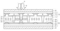
도 1은 종래 기술에 따른 터치 스크린 내장형 액정표시패널의 개략 단면도이다. 상기 도 1을 참조하면, 종래 기술에 따른 터치 스크린 내장형 액정표시패널은 다수의 컬러 필터(13)를 포함한 컬러 필터 기판(10)과, 다수의 화소를 포함한 박막 트랜지스터 기판(20), 상기 컬러 필터 기판(10)과 박막 트랜지스터 기판 사이에 주입된 액정층(30) 및 상기 양 기판 외측에 각각 부착된 편광판(41, 42)으로 구성되며, 상기 양 기판에는 도전성 컬럼 스페이서(17)와 상기 도전성 컬럼 스페이서와 소정 간격 이격되어 배치된 패드(27)로 구성된 센싱부가 형성되어, 터치 지점을 감지하게 된다.1 is a schematic cross-sectional view of a liquid crystal display panel with a touch screen according to the prior art. Referring to FIG. 1, a touch screen embedded LCD according to the related art includes a
상기와 같은 구조의 터치 스크린은 상판 즉, 컬러 필터 기판(10)에 대한 터치 동작을 통해서, 센서부의 작동을 유도한다. 즉, 상기 컬러 필터 기판(10)을 터치하게 되면, 상기 도전성 컬럼 스페이서(17)와 상기 패드(27)의 간극 변화가 발생되고, 이러한 간극 변화에 의해서, 예를 들면 터치 지점의 저항 변화가 발생된다. 그 결과, 상기 저항 변화 지점을 감지하여, 터치 지점을 감지하게 된다.The touch screen having the above structure induces an operation of the sensor unit through a touch operation on the upper plate, that is, the
그러나, 상기와 같은 구조에서 터치 감도(touch sensitivity)는 터치 환경에 의존성을 가진다. 즉, 터치 면적이 적으면서 일정 강도를 가지는 막대(bar)를 이용하여 터치하는 경우(A의 경우)에는 터치 감도가 높은 반면에, 터치 면적이 넓으면서, 소프트한 도구 예를 들면, 손가락 등으로 터치하는 경우(B의 경우)에는 터치 감도가 낮아지는 문제점이 있다.However, in such a structure, touch sensitivity has a dependency on the touch environment. In other words, when the touch is performed using a bar having a small intensity while having a small touch area (in case of A), the touch sensitivity is high, while the touch area is wide and soft with a soft tool such as a finger. In case of touching (in case of B), there is a problem in that the touch sensitivity is lowered.
본 발명은 상술한 종래의 문제점을 극복하기 위한 것으로서, 본 발명이 이루고자 하는 기술적 과제는 터치 환경에 관계없이 터치 감도(touch sensitivity)를 개선시킬 수 있는 터치 스크린 내장형 액정표시패널 및 이를 포함한 액정표시장치를 제공하기 위한 것이다.SUMMARY OF THE INVENTION The present invention has been made to overcome the above-described problems, and a technical problem to be achieved by the present invention is a touch screen embedded liquid crystal display panel capable of improving touch sensitivity regardless of a touch environment and a liquid crystal display including the same. It is to provide.
상기 본 발명의 목적을 달성하기 위한 본 발명의 일 측면에 따르면, 제1 기판; 상기 제1 기판과 대향되게 배치되는 제2 기판; 상기 제1 기판과 제2 기판 사이에 주입된 액정층; 터치 지점을 감지하기 위한, 도전성 컬럼 스페이서 및 상기 도전성 컬럼 스페이서와 소정 간격 이격된 채 배치되는 도전성 패드로 구성된 센싱부 및 상기 제1 기판 외측 상에 배치되며, 소정 경도를 갖는 다수의 가압 입자를 포함하는 것을 특징으로 하는 터치 스크린 내장형 액정표시패널이 제공된다.According to an aspect of the present invention for achieving the object of the present invention, a first substrate; A second substrate disposed to face the first substrate; A liquid crystal layer injected between the first substrate and the second substrate; A sensing unit including a conductive column spacer for sensing a touch point and a conductive pad spaced apart from the conductive column spacer by a predetermined distance, and a plurality of pressed particles disposed on the outside of the first substrate and having a predetermined hardness. Provided is a liquid crystal display panel with a built-in touch screen.
상기 제1 기판 및 상기 제2 기판 외측에 각각 부착되는 제1 편광판 및 제2 편광판을 더 포함한다.And a first polarizing plate and a second polarizing plate respectively attached to the outside of the first substrate and the second substrate.
상기 제1 기판은 절연성 투명 기판; 광을 차단하기 위한 블랙 매트릭스; 다수의 컬러 필터 및 상기 다수의 컬러 필터 전면에 형성된 공통 전극을 포함하며, 상기 도전성 컬럼 스페이서는 상기 제1 기판 상에 형성된다.The first substrate is an insulating transparent substrate; A black matrix for blocking light; A plurality of color filters and a common electrode formed on the front surface of the plurality of color filters, the conductive column spacer is formed on the first substrate.
상기 도전성 컬럼 스페이서는 상기 블랙 매트릭스 상에 형성된다.The conductive column spacer is formed on the black matrix.
상기 도전성 컬럼 스페이서는 절연성 재료로 이루어진 돌기부 및 상기 돌기부 상에 형성된 도전층으로 구성된다.The conductive column spacer is composed of a projection made of an insulating material and a conductive layer formed on the projection.
상기 도전성 컬럼 스페이서는 도전성 재료로 이루어진 돌기부로 구성된다.The conductive column spacer is composed of a projection made of a conductive material.
상기 제2 기판은 절연성 투명 기판; 상기 기판 상에 형성된 다수의 박막 트랜지스터 및 다수의 화소 전극을 포함하며, 상기 도전성 패드는 상기 제2 기판 상에 형성된다.The second substrate is an insulating transparent substrate; A plurality of thin film transistors and a plurality of pixel electrodes formed on the substrate, wherein the conductive pad is formed on the second substrate.
상기 제2 기판은 상기 도전성 패드와 전기적으로 연결된 다수의 제1 센싱 라인과 다수의 제2 센싱 라인을 더 포함한다.The second substrate further includes a plurality of first sensing lines and a plurality of second sensing lines electrically connected to the conductive pads.
상기 도전성 패드는 상기 화소 전극과 동일한 재료로 형성된다.The conductive pad is formed of the same material as the pixel electrode.
상기 제1 기판과 제2 기판 사이의 액정 셀 갭을 유지하기 위한 스페이서를 더 포함한다.The semiconductor device may further include a spacer for maintaining a liquid crystal cell gap between the first substrate and the second substrate.
상기 스페이서는 볼 스페이서 또는 컬럼 스페이서를 포함한다.The spacer comprises a ball spacer or column spacer.
상기 가압 입자는 볼(ball) 형태인 것을 특징으로 한다.The pressurized particles are characterized in that the ball (ball) form.
상기 가압 입자의 크기는 1㎛ ~ 100㎛ 인 것을 특징으로 한다.The pressed particles have a size of 1 μm to 100 μm.
상기 가압 입자는 투명성 재료로 형성되는 것을 특징으로 한다.The pressurized particles are characterized in that formed of a transparent material.
상기 다수의 가압 입자는 상기 도전성 컬럼 스페이서 및 도전성 패드에 상응하는 위치에 적하되는 것을 특징으로 한다.The plurality of pressurized particles are dropped in a position corresponding to the conductive column spacer and the conductive pad.
상기 다수의 가압 입자는 소정의 분산 밀도로 상기 제1 기판의 외측 상에 산포되는 것을 특징으로 한다.The plurality of pressurized particles are characterized in that the dispersed on the outside of the first substrate at a predetermined dispersion density.
상기 다수의 가압 입자는 소정의 분산 밀도로 상기 제1 편광판의 점착층 상에 산포되는 것을 특징으로 한다.The plurality of pressurized particles are characterized in that the dispersed on the pressure-sensitive adhesive layer of the first polarizing plate at a predetermined dispersion density.
상기 센싱부로부터의 신호를 입력 받아, 전압 변화를 감지하여, 터치 지점의 좌표를 생성하기 위한 제어부 및 상기 제어부로부터의 좌표를 입력 받아, 포인터를 동작시키기 위한 드라이버를 더 포함한다.The controller may further include a controller for receiving a signal from the sensing unit, sensing a voltage change, generating coordinates of a touch point, and receiving a coordinate from the controller and operating a pointer.
한편, 본 발명의 다른 측면에 따르면, 제1 기판과, 상기 제1 기판과 대향되게 배치되는 제2 기판과, 상기 제1 기판과 제2 기판 사이에 주입된 액정층과, 터치 지점을 감지하기 위하여, 도전성 컬럼 스페이서 및 상기 도전성 컬럼 스페이서와 소정 간격 이격된 채 배치되는 도전성 패드로 구성된 센싱부 및 상기 제1 기판 외측 상에 배치되며, 소정 경도를 갖는 다수의 가압 입자를 포함하는 터치 스크린 내장형 액정표시패널 및 상기 액정표시패널에 광을 제공하기 위한 백라이트를 포함하는 것을 특징으로 하는 액정표시장치가 제공된다.Meanwhile, according to another aspect of the present invention, a first substrate, a second substrate disposed to face the first substrate, a liquid crystal layer injected between the first substrate and the second substrate, and detecting a touch point To this end, a sensing unit comprising a conductive column spacer and a conductive pad disposed to be spaced apart from the conductive column spacer by a predetermined distance, and a touch screen embedded liquid crystal including a plurality of pressurized particles disposed on the outside of the first substrate and having a predetermined hardness. A liquid crystal display device comprising a display panel and a backlight for providing light to the liquid crystal display panel.
한편, 층, 막, 영역, 판 등의 부분이 다른 부분 상부에 또는 위에 있다고 표현되는 경우는 각 부분이 다른 부분의 바로 상부 또는 바로 위에 있는 경우 뿐만 아니라 각 부분과 다른 부분의 사이에 또 다른 부분이 있는 경우도 포함한다.On the other hand, when a part such as a layer, a film, an area, or a plate is expressed as being on or above another part, not only when each part is directly above or directly above the other part but also another part between each part and another part This includes cases.
이하, 첨부된 도면을 참조하여 본 발명의 바람직한 실시예에 대해 상세히 설명한다.Hereinafter, with reference to the accompanying drawings will be described in detail a preferred embodiment of the present invention.
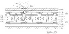
도 2는 본 발명에 따른 터치 스크린 내장형 액정표시패널의 개략 단면도이다.2 is a schematic cross-sectional view of a touch screen embedded liquid crystal display panel according to the present invention.
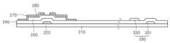
상기 도 2를 참조하면, 상기 터치 스크린 내장형 액정표시패널은 컬러 필터 기판(100), 박막 트랜지스터 기판(200), 센싱부(300), 액정층(400), 편광판(500) 및 가압 입자(600)를 포함한다.Referring to FIG. 2, the touch screen embedded liquid crystal display panel includes a
상기 컬러 필터 기판(100)은 절연성 투명 기판(110), 상기 절연성 투명 기판 상에 형성되어, 광을 차단하기 위한 블랙 매트릭스(120), 상기 절연성 투명 기판과 블랙 매트릭스 상에 형성되는 다수의 적색(Red), 녹색(Green), 청색(Blue) 컬러 필터(130) 및 상기 다수의 컬러 필터의 전면에 형성된 공통 전극(140)을 포함하며, 또한, 상기 센싱부(300)의 도전성 컬럼 스페이서(310)를 포함한다.The
상기 박막 트랜지스터 기판(200)은 절연성 투명 기판(210), 상기 절연성 투명 기판 상에 형성된 다수의 박막 트랜지스터(미도시)와, 다수의 화소 전극(290)을 포함하며, 또한 상기 센싱부(300)의 도전성 패드(320)를 포함한다.The thin
상기 컬러 필터 기판(100)과 상기 박막 트랜지스터 기판(200)의 사이에는 액정층(400)이 주입되며, 상기 컬러 필터 기판(100)과 상기 박막 트랜지스터 기판(200)의 외측에는 제1 편광판(510)과 제2 편광판(520)이 각각 배치되고, 상기 컬러 필터 기판(100)과 상기 박막 트랜지스터 기판(200) 사이에는 양 기판의 셀 갭을 유지하기 위한 스페이서(450)가 배치된다. 본 실시예에서는 컬럼 스페이서가 배치되나, 이에 한정되는 것은 아니며, 볼 스페이서가 배치될 수도 있다.The
또한, 상기 센싱부(300)는 상기 컬러 필터 기판(100) 상에 형성된 도전성 컬럼 스페이서(310)와 박막 트랜지스터 기판(200) 상에 형성된 도전성 패드(320)로 구성되며, 상기 도전성 컬럼 스페이서(310)와 상기 도전성 패드(320)는 소정 간격 이격된 채, 상호 대응되는 위치에 배치된다. 상기 센싱부(300)는 상기 도전성 컬럼 스페이서(310)와 도전성 패드(320)의 간극 변화에 따른 저항 변화를 감지하여, 터치 지점을 감지하게 된다. 즉, 사용자가 소정 위치를 터치하게 되면, 상기 위치에 대응되는 상기 도전성 컬럼 스페이서(310)는 하방 즉, 도전성 패드(320) 방향으로 힘으로 받게 되어, 상기 도전성 패드와 접촉하게 된다. 그리고 나서, 사용자의 터치가 제거되면, 상기 위치에 작용하는 힘이 제거되면서, 상기 도전성 컬럼 스페이서(310)와 도전성 패드(320)는 원래대로 소정 간격 이격된 채 배치된다. 이와 같이, 소정 위치를 터치하면, 상기 도전성 컬럼 스페이서(310)와 도전성 패드(320) 간의 쇼트(short)와 오픈(open)이 발생하면서, 상기 위치에서 저항 변화가 생기며, 이에 따라 변화하는 전압을 감지하여, 터치되는 지점을 감지할 수 있게 된다.In addition, the
한편, 상기 소정 경도를 갖는 가압 입자(600)는 상기 컬러 필터 기판(100)과 상기 제1 편광판(510) 사이에 배치되어, 상기 컬러 필터 기판(100)의 최외측에 배치된 제1 편광판(510)을 통해서 전달되는 힘이 국부 영역 즉, 상기 도전성 컬럼 스페이서(310)에 상응하는 영역에 집중될 수 있도록, 가압 범위를 전환시키는 기능을 수행한다. 상기 가압 입자(600)의 경도는 상기 제1 편광판(510) 및 상기 절연성 투명 기판(110)의 경도와 유사하거나 크게 형성하는 것이 바람직하다.On the other hand, the
또한, 상기 가압 입자(600)는 다양한 형태로 형성될 수 있으나, 볼(ball) 형태로 형성되는 것이 바람직하며, 상기 가압 입자(600)의 크기는 1㎛ ~ 100㎛로 형성되며, 실리케이트 등과 같은 투명성 재료로 형성하는 것이 바람직하다. 예를 들면, 투명한 글라스 비드(glass bead)를 사용할 수 있다. 또한, 이때 가압 입자의 크기가 너무 작으면, 터치 압력의 가압력을 집중시키기가 어려워지고, 가압 입자의 크기가 너무 크면 액정표시패널에서 출력되는 화상에 악영향을 줄 수 있는 바, 상기와 같이 1㎛ ~ 100㎛의 크기로 형성하는 것이 바람직하다.In addition, the
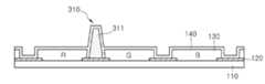
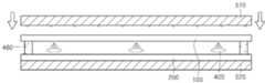
도 3은 본 발명에 따른 터치 스크린 내장형 액정표시패널의 터치 동작을 나타낸 도이다. 상기 도 3에는 상기에서 살펴본 바와 같이, 상기 컬러 필터 기판(100)과 제1 편광판(510) 사이에 가압 입자(600)가 배치된 터치 스크린 내장형 액정표시패널의 터치 동작이 도시된다. 본 실시예에서는 터치 면적이 넓으면서, 소프트한 도구 예를 들면, 사용자의 손가락 등으로 터치하는 경우가 도시된다.3 illustrates a touch operation of a touch screen embedded liquid crystal display panel according to the present invention. 3 illustrates a touch operation of the touch screen embedded liquid crystal display panel in which the
일반적으로, 딱딱하면서, 액정표시패널과의 접촉 면적이 적은 터치 도구를 사용하는 환경 즉, 터치 면적이 적으면서 일정 강도를 가지는 펜 형태의 막대(bar)를 이용하여 터치하는 경우에는 터치 압력의 대부분이 상기 센싱부(300)의 도전성 컬럼 스페이서(310)와 도전성 패드(320)의 간극거리 변화에 사용되는 반면에, 소프트하면서, 액정표시패널과의 접촉 면적이 큰 터치 도구 즉, 사용자의 손가락 등으로 터치하는 경우에는 터치 압력의 대분분이 간극거리 변화보다 기판의 변형력으로 전환되기 때문에, 상기 컬럼 스페이서(310)와 도전성 패드(320)의 간극거리 변화를 위해서는 보다 큰 터치 압력이 필요하게 된다.In general, most of the touch pressure is hard when touched with an environment using a touch tool having a small contact area with a liquid crystal display panel, that is, a pen-shaped bar having a small intensity while having a small touch area. While it is used to change the gap distance between the
반면, 상기 컬러 필터 기판(100)과 제1 편광판(510) 사이에 가압 입자(600)가 배치된 본 발명에 따른 터치 스크린 내장형 액정표시패널을 사용자의 손가락 등으로 터치하게 되면, 상기 가압 입자(600)에 의해서 터치 압력의 가압 범위가 국소 영역 즉, 상기 도전성 컬럼 스페이서(310) 영역 상에 집중되도록 전환된다. 그 결과, 소프트하면서, 액정표시패널과의 접촉 면적이 큰 터치 도구를 사용하여 터치하더라도, 딱딱하면서, 액정표시패널과의 접촉 면적이 적은 터치 도구를 사용하여 터 치하는 것과 동일한 효과를 얻게 된다.On the other hand, when the touch screen embedded liquid crystal display panel according to the present invention having the
도 4는 본 발명에 따른 터치 스크린 내장형 액정표시패널의 터치 스크린의 개략적인 기능 블록도이다.4 is a schematic functional block diagram of a touch screen of a touch screen embedded liquid crystal display panel according to the present invention.
상기 도 4를 참조하면, 상기 터치 스크린은 센싱부(300), 제어부(350) 및 드라이버(360)를 포함한다. 상기 센싱부(300)은 상기에서 살펴본 바와 같이, 상기 컬러 필터 기판(100) 상에 형성된 도전성 컬럼 스페이서(310)와 상기 박막 트랜지스터 기판(200) 상에 형성된 도전성 패드(320)로 구성되어, 상기 도전성 컬럼 스페이서(310)와 도전성 패드(320)의 간극 변화에 따른 저항의 변화가 생기며, 이에 따라 변화하는 전압을 감지하게 된다.Referring to FIG. 4, the touch screen includes a
상기 제어부(350)는 상기 센싱부(300)로부터의 신호를 입력 받아서, 전압 변화를 감지하여, 그에 상응하는 좌표를 생성하게 된다. 상기 제어부(350)에 의해 생성된 좌표는 상기 드라이버(360)로 전달되며, 상기 드라이버(360)에서는 이러한 좌표를 받아서, 포인터를 동작하게 된다.The
상기 제어부(350) 및 드라이버(360)는 상기 액정표시패널의 일 측에 실장될 수 있으며, 상기 액정표시패널과 전기적으로 연결된 회로기판 상에 실장될 수도 있다.The
도 5는 본 발명에 따른 터치 스크린 내장형 액정표시패널의 개략 평면도이다.상기 도 5에는 본 발명에 따른 터치 스크린 내장형 액정표시패널의 컬러 필터 기판(100)과 박막 트랜지스터 기판(200)의 부분 평면도가 도시된다.5 is a schematic plan view of a touch screen embedded liquid crystal display panel according to the present invention. FIG. 5 is a partial plan view of the
상기 컬러 필터 기판(100)의 투명 절연성 기판 상에는 적색, 녹색 및 청색 컬러 필터(130)가 형성되며, 상기 각 컬러 필터의 사이 영역 즉, 블랙 매트릭스 영역 상에는 도전성 컬럼 스페이서(310)가 배치된다. 본 실시예에서, 상기 도전성 컬럼 스페이서(310)는 단위 화소 당 한 개씩이 배치되어 있으나, 상기 도전성 컬럼 스페이서의 개수 및 형태는 다양하게 변형될 수 있다.The red, green, and
또한, 상기 컬러 필터 기판(100)과 대향되게 배치되는 박막 트랜지스터 기판(200)에는 절연성 투명 기판 상에 게이트 신호를 전달하며 제1 방향으로 연장되어 배치된 게이트 라인(220)과, 상기 게이트 라인(220)과 절연되게 교차되며, 제2 방향으로 연장되어 배치된 데이터 라인(270)과, 상기 게이트 라인(220)과 데이터 라인(270)에 의해 정의된 화소 영역에 형성된 화소 전극(290)과, 상기 화소 전극과 접속되고 게이트 라인(220)과 데이터 라인(270)의 교차점에 매트릭스 형태로 형성된 복수의 박막 트랜지스터를 포함한다. 또한, 상기 박막 트랜지스터 기판(200) 상에는 상기 게이트 라인(220)과 소정 간격 이격되어 배치된 제1 센싱 라인(331)과 상기 데이터 라인(270)과 소정 간격 이격되어 배치된 제2 센싱 라인(333)이 형성된다.In addition, the thin
상기 도전성 패드(320)는 도전성 컬럼 스페이서(310)에 상응하는 영역 즉, 상기 제1 센싱 라인(331)과 제2 센싱 라인(333)의 교차 영역 상부에 형성되며, 상기 도전성 패드(320)는 상기 제1 센싱 라인(331)과 상기 제2 센싱 라인(333)과 콘택된다. 이때, 상기 도전성 패드(320)는 상기 컬러 필터 기판(100)과 박막 트랜지 스터 기판(200)의 합착 시, 상기 도전성 컬럼 스페이서(310)와 소정 간격 이격된 채 배치되도록 형성된다.The
상기와 같은 구조의 터치 스크린 내장형 액정표시패널에서 사용자의 터치 동작이 발생하게 되면, 터치 압력이 상기 도전성 컬럼 스페이서(310)에 전달되어, 상기 도전성 컬럼 스페이서(310)는 이에 상응하는 도전성 패드(320)와 접촉하게 되어, 접촉 위치에서는 저항 변화가 생겨서, 전압이 변화하게 되고, 이러한 전압 변화는 상기 제1 센싱 라인(331)과 제2 센싱 라인(333)을 통하여, 상기의 제어부(350)로 전달되고, 상기 제어부(350)에서는 전압 변화를 감지하여, 그에 상응하는 좌표를 생성하게 된다.When a user's touch operation occurs in the touch screen embedded liquid crystal display panel having the above structure, touch pressure is transmitted to the
한편, 본 실시예에서, 상기 도전성 패드(320)는 상기 화소 전극(290)과 소정 간격 이격된 채, 상기 제1 센싱 라인(331)과 제2 센싱 라인(333)의 교차 영역 상부에 형성되나, 이에 한정되는 것은 아니며, 상기 도전성 컬럼 스페이서(310)와 상응하는 위치에 한하여, 다양한 영역 상에 형성될 수도 있다.Meanwhile, in the present exemplary embodiment, the
도 6a 내지 도 6d는 본 발명에 따른 터치 스크린 내장형 액정표시패널의 컬러 필터 기판의 일 예를 제조하기 위한 공정 단면도로서, 상기 도 5에 도시된 터치 스크린 내장형 액정표시패널의 Ⅰ-Ⅰ선에 따른 컬러 필터 기판의 제조 공정 단면도이다.6A to 6D are cross-sectional views illustrating a process of manufacturing an example of a color filter substrate of a touch screen embedded liquid crystal display panel according to the present invention, and taken along line I-I of the touch screen embedded liquid crystal display panel shown in FIG. It is sectional drawing of a manufacturing process of a color filter board | substrate.
상기 상기 도 6a를 참조하면, 우선, 절연성 투명 기판(110) 상에 블랙 매트릭스(120)를 형성한다. 이때, 상기 절연성 투명 기판, 통상적으로 유리 기판을 사 용하며, 상기 블랙 매트릭스는 크롬 등의 금속 박막이나 카본 계열의 유기 재료를 사용하여 형성한다. 또한, 블랙 매트릭스(120)는 각 화소의 경계 부근에 설치되어, 컬러 필터를 각각 분리하는 동시에, 박막 트랜지스터 기판의 화소 전극이 제어하지 못하는 영역의 액정 셀을 통과해 나오는 광을 차단하여, 액정 표시 장치의 콘트라스트비를 향상시킨다.Referring to FIG. 6A, first, a
상기 도 6b를 참조하면, 상기 블랙 매트릭스(120)가 형성된 기판(110) 상에 다수의 컬러 필터(130) 예를 들면, 적색(R), 청색(B) 및 녹색(G) 컬러 필터가 형성된다. 이러한 컬러 필터(130)를 형성하는 과정을 살펴보면, 기판 상에 적색 성분의 안료가 분산된 네가티브 컬러 포토레지스트를 도포한 후, 마스크를 사용하여 노광한다. 이때, 마스크는 적색 컬러 필터가 형성될 영역을 개방한 후, 상기 영역들을 노광시킨다. 그 다음에, 현상액을 이용하여 네가티브 컬러 포토레지스트를 현상하면, 노광된 영역의 광 중합 개시제가 반응하여 폴리머가 형성되므로, 현상 시 제거되지 않고 패턴으로 남게 되며, 나머지 노광되지 않은 영역만이 제거된다. 그 결과, 기판 상에는 적색 컬러 필터가 형성되며, 상기와 같은 과정을 반복하여 청색 컬러 필터 및 녹색 컬러 필터가 형성된다.Referring to FIG. 6B, a plurality of
상기 도 6c를 참조하면, 상기 블랙 매트릭스(120) 상에는 돌기부(311)가 소정 간격으로 형성된다. 이러한 돌기부(311)를 형성하는 과정을 살펴보면, 상기 다수의 컬러 필터 전면에 돌기부(311) 형성을 위한 유기 절연막 또는 무기 절연막을 도포한 후, 마스크를 이용한 포토리소그라피 공정을 실시하여 상기 돌기부(311)를 형성한다.Referring to FIG. 6C,
도 6d를 참조하면, 상기 다수의 컬러 필터(130) 및 상기 돌기부(311)의 전면에 공통 전극(140)으로서 투명 전도층이 스퍼터링 등의 방법으로 형성된다. 이때, 상기 공통 전극(140)은 인듐 틴 옥사이드(ITO) 또는 인듐 징크 옥사이드(IZO)가 사용될 수 있다. 상기와 같은 컬러 필터 기판의 제조 공정에 의하면, 상기 돌기부(311) 상에 투명 전도층이 형성됨으로써, 도전성 컬럼 스페이서(310)를 형성하게 된다.Referring to FIG. 6D, a transparent conductive layer is formed on the front of the plurality of
상기 공통 전극(140) 형성시 양호한 스텝 커버리지를 위하여, 다수의 컬러 필터(130) 상에 오버코트막이 형성될 수도 있다.In order to provide good step coverage when forming the
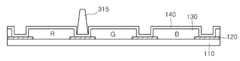
도 7은 본 발명에 따른 터치 스크린 내장형 액정표시패널의 컬러 필터 기판의 다른 예를 도시한 단면도이다.7 is a cross-sectional view showing another example of a color filter substrate of a liquid crystal display panel with a touch screen according to the present invention.
상기 도 7을 참조하면, 상기 컬러 필터 기판은 절연성 투명 기판(110), 블랙 매트릭스(120), 다수의 컬러 필터(130), 도전성 돌기부로 구성된 도전성 컬럼 스페이서(315) 및 공통 전극(140)을 포함한다.Referring to FIG. 7, the color filter substrate includes an insulating
상기 절연성 투명 기판(110) 예를 들면, 유리 기판 상에 블랙 매트릭스(120)가 형성된다. 상기 블랙 매트릭스(120)가 형성된 기판(110) 상에 다수의 컬러 필터(130) 예를 들면, 적색(R), 청색(B) 및 녹색(G) 컬러 필터가 형성된다. 그리고, 상기 다수의 컬러 필터(130)의 전면에 공통 전극(140)으로서 투명 전도층이 스퍼터링 등의 방법으로 형성되며, 상기 공통 전극(140) 상에는 소정 간격으로 도전성 재료로 이루어진 돌기부 즉, 도전성 컬럼 스페이서(315)가 형성된다.The
도 8a 내지 도 8e는 본 발명에 따른 터치 스크린 내장형 액정표시패널의 박막 트랜지스터 기판의 일 예를 제조하기 위한 공정 단면도로서, 상기 도 5에 도시된 터치 스크린 내장형 액정표시패널의 Ⅱ-Ⅱ선에 따른 박막 트랜지스터 기판의 제조 공정 단면도이다.8A to 8E are cross-sectional views illustrating a process of manufacturing an example of a thin film transistor substrate of a touch screen embedded liquid crystal display panel according to an embodiment of the present invention, and taken along line II-II of the touch screen embedded liquid crystal display panel shown in FIG. It is sectional drawing of a manufacturing process of a thin film transistor substrate.
우선 도 8a를 참조하면, 절연성 투명 기판(210) 상에 제1 도전성막을 형성한 다음, 이를 제 1 감광막 마스크 패턴(미도시)을 이용한 식각공정을 통해 소정 선폭의 게이트 전극 및 스토리지 커패시터 전극(미도시)을 포함하는 게이트 라인 및 제1 센싱 라인(331)을 형성한다.Referring to FIG. 8A, a first conductive layer is formed on an insulating
상기 도 8b를 참조하면, 상기 도 8a에 도시된 기판 전면에 게이트 절연막(240), 활성층(250) 및 오믹 접촉층(260)을 순차적으로 형성한 다음, 제2 감광막 마스크 패턴(미도시)을 이용한 식각공정을 실시하여 박막 트랜지스터의 활성영역을 형성한다. 이때, 게이트 절연막(240)으로는 산화 실리콘 또는 질화 실리콘을 포함하는 무기 절연 물질을 사용하는 것이 바람직하다. 상기 활성층(250)으로는 비정질 실리콘층을 사용하고, 오믹 접촉층(260)으로는 실리사이드 또는 N형 불순물이 고농도로 도핑된 비정질 실리콘층을 사용한다.Referring to FIG. 8B, the
도 8c를 참조하면, 박막 트랜지스터의 활성 영역이 형성된 기판 전면에 제2 도전성막을 형성한 다음, 이를 제3 감광막 마스크 패턴(미도시)을 이용하여 식각을 실시하여 소스 전극 및 드레인 전극을 포함하는 데이터 라인(270) 및 제2 센싱 라인(333)을 형성한다.Referring to FIG. 8C, data including a source electrode and a drain electrode is formed by forming a second conductive layer on the entire surface of the substrate on which the active region of the thin film transistor is formed, and then etching the same using a third photoresist mask pattern (not shown).
상기 도 8d를 참조하면, 박막 트랜지스터와 데이터 라인이 형성된 기판 전면에 보호막(280)을 형성하고, 제 4 감광막 마스크 패턴를 이용한 식각공정을 통해 유기막(280)의 일부를 제거하여 상기 드레인 전극과 이하의 화소 전극을 콘택시키기 위한 콘택홀을 형성하며, 상기 제1 센싱 라인(331)과 상기 제2 센싱 라인(333)과 이하의 도전성 패드를 콘택시키기 위한 콘택홀을 각각 형성한다.Referring to FIG. 8D, the
상기 도 8e를 참조하면, 상기 보호막(280) 상에 제 3 도전성막을 형성한 다음, 제 5 감광막 마스크 패턴(미도시)을 이용하여 제 3 도전성막을 패터닝하여 화소 전극(290) 및 도전성 전극 패드(320)를 형성한다. 이때, 제 3 도전성막은 ITO나 IZO를 포함하는 투명 도전막을 사용하는 것이 바람직하며, 상기 도전성 전극 패드(320)는 상기 화소 전극(290)과 소정 간격 이격된 채, 상기 제1 센싱 라인(331)과 제2 센싱 라인(333)의 교차 영역 상에 형성된다.Referring to FIG. 8E, a third conductive layer is formed on the
도 9a 내지 도 11b는 본 발명에 따른 터치 스크린 내장형 액정표시패널에 가압 입자를 배치하기 위한 방법을 각각 도시한 도이다.9A to 11B are views illustrating a method for arranging pressurized particles in a touch screen embedded liquid crystal display panel according to the present invention, respectively.
상기 도 9a 및 도 9b에 도시된 방법을 살펴보면, 우선 터치 스크린 내장형 액정표시패널의 컬러 필터 기판(100) 상에 가압 입자(600)를 스프레이 방법으로 분사하여, 소정의 분산 밀도로 산포시킨다(도 9a). 이때, 상기 가압 입자(600)를 용제와 혼합하여 분사시킬 수도 있으며, 공기 또는 질소 등을 이용하여 분사시킬 수도 있다. 그리고 나서, 상기 액정표시패널의 외측에 편광판(510, 520)을 부착시킨다(도 9b).9A and 9B, first,
상기 도 10a 및 도 10b에 도시된 방법을 살펴보면, 상기 컬러 필터 기판(100)의 외측에 부착될 제1 편광판(510)의 점착층 상에 가압 입자(600)를 스프레이 방법으로 분사하여, 소정의 분산 밀도로 산포시킨다(도 10a). 이때, 상기 가압 입자(600)를 용제와 혼합하여 분사시킬 수도 있으며, 공기 또는 질소 등을 이용하여 분사시킬 수도 있다. 그리고 나서, 상기 가압 입자(600)가 배치된 상기 제1 편광판(510)을 상기 컬러 필터 기판(100)의 외측에 부착시킨다(도 10b).10A and 10B, the
상기 도 10a 및 도 10b에 도시된 방법을 살펴보면, 우선 가압 입자(600)를 디스펜서를 이용하여 상기 컬러 필터 기판(100)의 소정 영역 즉, 도전성 컬럼 스페이서의 상부 영역에 적하시킨다(도 10a). 그리고 나서, 상기 액정표시패널의 외측에 편광판(510, 520)을 부착시킨다(도 10b).Referring to the method illustrated in FIGS. 10A and 10B, first, the
한편, 상기와 같은 액정표시패널에 광을 제공하기 위하여, 다수의 광학 시트,백램프 유닛, 반사판 및 도광판 등을 포함하는 백라이트를 상기 액정표시패널의 하부에 배치하여, 액정표시장치를 구현할 수 있다.Meanwhile, in order to provide light to the liquid crystal display panel as described above, a backlight including a plurality of optical sheets, a back lamp unit, a reflector, a light guide plate, and the like may be disposed under the liquid crystal display panel to implement a liquid crystal display device. .
이상에서 설명한 것은 본 발명에 따른 터치 스크린 내장형 액정표시패널 및 이를 포함한 액정표시장치의 예시적인 실시예에 불과한 것으로서, 본 발명은 상기한 실시예에 한정되지 않고, 이하의 특허청구범위에서 청구하는 바와 같이, 본 발명의 요지를 벗어남이 없이 당해 발명이 속하는 분야에서 통상의 지식을 가진 자라면 누구든지 다양한 변경 실시가 가능한 범위까지 본 발명의 기술적 정신이 있다고 할 것이다.What has been described above is merely an exemplary embodiment of a touch screen built-in liquid crystal display panel and a liquid crystal display device including the same, and the present invention is not limited to the above-described embodiment, and is claimed in the following claims. Likewise, without departing from the gist of the present invention, any person having ordinary knowledge in the field of the present invention will have the technical spirit of the present invention to the extent that various modifications can be made.
전술한 바와 같이 본 발명에 따르면, 가압 입자가 배치된 터치 스크린 내장형 액정표시패널에 따르면, 이러한 가압 입자에 의해서 터치 압력의 가압 범위가 국소 영역 상에 집중되도록 전환되어, 소프트하면서, 액정표시패널과의 접촉 면적이 큰 터치 도구를 사용하여 터치하더라도, 딱딱하면서, 액정표시패널과의 접촉 면적이 적은 터치 도구를 사용하여 터치하는 것과 동일한 효과를 얻을 수 있게 된다. 그 결과, 터치 환경에 관계없이 일정 수준의 터치 감도를 유지할 수 있게 된다.As described above, according to the present invention, according to the touch screen-embedded liquid crystal display panel in which the pressurized particles are arranged, the pressurized range of the touch pressure is switched by the pressurized particles so as to be concentrated on the local area, and soft and the liquid crystal display panel is provided. Even if the touch is touched using a touch tool having a large contact area, the same effect as that of touching using a touch tool that is hard and has a small contact area with the liquid crystal display panel can be obtained. As a result, a certain level of touch sensitivity can be maintained regardless of the touch environment.
Claims (19)
Translated fromKoreanPriority Applications (2)
| Application Number | Priority Date | Filing Date | Title |
|---|---|---|---|
| KR1020060041786AKR101254695B1 (en) | 2006-05-10 | 2006-05-10 | Liquid crystal display panel with a built-in touch screen and liquid crystal display having the same |
| US11/745,284US7675580B2 (en) | 2006-05-10 | 2007-05-07 | Liquid crystal display with built-in touch screen having particles for pressure concentration |
Applications Claiming Priority (1)
| Application Number | Priority Date | Filing Date | Title |
|---|---|---|---|
| KR1020060041786AKR101254695B1 (en) | 2006-05-10 | 2006-05-10 | Liquid crystal display panel with a built-in touch screen and liquid crystal display having the same |
Publications (2)
| Publication Number | Publication Date |
|---|---|
| KR20070109180A KR20070109180A (en) | 2007-11-15 |
| KR101254695B1true KR101254695B1 (en) | 2013-04-23 |
Family
ID=38684652
Family Applications (1)
| Application Number | Title | Priority Date | Filing Date |
|---|---|---|---|
| KR1020060041786AExpired - Fee RelatedKR101254695B1 (en) | 2006-05-10 | 2006-05-10 | Liquid crystal display panel with a built-in touch screen and liquid crystal display having the same |
Country Status (2)
| Country | Link |
|---|---|
| US (1) | US7675580B2 (en) |
| KR (1) | KR101254695B1 (en) |
Cited By (1)
| Publication number | Priority date | Publication date | Assignee | Title |
|---|---|---|---|---|
| US10684713B2 (en) | 2016-04-07 | 2020-06-16 | Samsung Display Co., Ltd. | Display device and manufacturing method of the same |
Families Citing this family (84)
| Publication number | Priority date | Publication date | Assignee | Title |
|---|---|---|---|---|
| US7663607B2 (en) | 2004-05-06 | 2010-02-16 | Apple Inc. | Multipoint touchscreen |
| US20070283832A1 (en)* | 2006-06-09 | 2007-12-13 | Apple Computer, Inc. | Imprint circuit patterning |
| US8259078B2 (en) | 2006-06-09 | 2012-09-04 | Apple Inc. | Touch screen liquid crystal display |
| CN104965621B (en) | 2006-06-09 | 2018-06-12 | 苹果公司 | Touch screen LCD and its operating method |
| CN102981678B (en) | 2006-06-09 | 2015-07-22 | 苹果公司 | Touch screen liquid crystal display |
| KR20080011873A (en)* | 2006-08-01 | 2008-02-11 | 삼성전자주식회사 | Electrophoresis display |
| CN101191915B (en)* | 2006-11-24 | 2010-05-19 | 群康科技(深圳)有限公司 | Liquid crystal display panel |
| KR101395223B1 (en)* | 2006-12-04 | 2014-05-16 | 삼성디스플레이 주식회사 | Liquid crystal display device |
| KR20080053035A (en)* | 2006-12-08 | 2008-06-12 | 삼성전자주식회사 | Electrophoretic display |
| KR20080052836A (en)* | 2006-12-08 | 2008-06-12 | 삼성전자주식회사 | Liquid Crystal Display and Manufacturing Method Thereof |
| US8493330B2 (en) | 2007-01-03 | 2013-07-23 | Apple Inc. | Individual channel phase delay scheme |
| US7812827B2 (en)* | 2007-01-03 | 2010-10-12 | Apple Inc. | Simultaneous sensing arrangement |
| US9710095B2 (en) | 2007-01-05 | 2017-07-18 | Apple Inc. | Touch screen stack-ups |
| KR101385190B1 (en)* | 2007-02-07 | 2014-04-15 | 삼성디스플레이 주식회사 | Liquid crystal display and manufacturing method of the same |
| US8493331B2 (en) | 2007-06-13 | 2013-07-23 | Apple Inc. | Touch detection using multiple simultaneous frequencies |
| TWI329221B (en)* | 2007-09-04 | 2010-08-21 | Au Optronics Corp | Touch panel |
| KR20090026576A (en)* | 2007-09-10 | 2009-03-13 | 삼성전자주식회사 | Display device and manufacturing method thereof |
| US20090115741A1 (en)* | 2007-11-06 | 2009-05-07 | Wintek Corporation | Touch sensor and touch screen panel |
| KR20090075369A (en)* | 2008-01-04 | 2009-07-08 | 삼성전자주식회사 | Display panel |
| KR101519844B1 (en)* | 2008-01-07 | 2015-05-13 | 삼성디스플레이 주식회사 | Upper Substrate For Touch Screen Panel, Method Of Manufacturing The Same And Display Device Having The Same |
| KR101415086B1 (en)* | 2008-02-15 | 2014-07-07 | 엘지디스플레이 주식회사 | Liquid crystal display |
| KR101471547B1 (en)* | 2008-02-20 | 2014-12-11 | 삼성디스플레이 주식회사 | Liquid crystal display |
| TWI363896B (en)* | 2008-03-28 | 2012-05-11 | Au Optronics Corp | Liquid crystal display panel and method of making the same |
| KR101472838B1 (en)* | 2008-04-11 | 2014-12-15 | 삼성디스플레이 주식회사 | Display panel assembly and display device including the same |
| KR100986491B1 (en)* | 2008-04-15 | 2010-10-08 | 엘지이노텍 주식회사 | Display |
| TWI372267B (en)* | 2008-04-28 | 2012-09-11 | Au Optronics Corp | Touch panel, color filter substrate and fabricating method thereof |
| US8508495B2 (en) | 2008-07-03 | 2013-08-13 | Apple Inc. | Display with dual-function capacitive elements |
| TWI375485B (en)* | 2008-07-04 | 2012-10-21 | Au Optronics Corp | Electroluminescent display touch panel |
| US20100007627A1 (en)* | 2008-07-09 | 2010-01-14 | Chi Hsin Electronics Corp. | Touch signal transmission circuit and liquid crystal display using the same |
| FR2934921B1 (en)* | 2008-08-05 | 2010-09-24 | Stantum | MULTICONTACT TOUCH SENSOR WITH VARIABLE SIZE AND IMPEDANCE SPACING MEANS |
| TWI389016B (en)* | 2008-08-26 | 2013-03-11 | Acer Inc | Integrated pixel structure, integrated touch panel lcd device and method of controlling the same |
| KR101500425B1 (en)* | 2008-08-27 | 2015-03-09 | 삼성디스플레이 주식회사 | Touch screen display apparatus |
| US9348451B2 (en) | 2008-09-10 | 2016-05-24 | Apple Inc. | Channel scan architecture for multiple stimulus multi-touch sensor panels |
| US8592697B2 (en) | 2008-09-10 | 2013-11-26 | Apple Inc. | Single-chip multi-stimulus sensor controller |
| US9606663B2 (en) | 2008-09-10 | 2017-03-28 | Apple Inc. | Multiple stimulation phase determination |
| US8508678B2 (en)* | 2008-09-25 | 2013-08-13 | Sharp Kabushiki Kaisha | Liquid crystal display device, touch panel, and display device including the same |
| JP5056702B2 (en) | 2008-09-29 | 2012-10-24 | カシオ計算機株式会社 | Liquid crystal display element and liquid crystal display device |
| KR101564332B1 (en)* | 2008-10-28 | 2015-10-30 | 삼성전자주식회사 | Touch screen panel integrated into a liquid crystal display, manufacturing method thereof, and touch sensing method |
| TWI384273B (en)* | 2008-10-31 | 2013-02-01 | Au Optronics Corp | Touch display panel |
| US8144295B2 (en) | 2008-11-18 | 2012-03-27 | Apple Inc. | Common bus design for a TFT-LCD display |
| JP5267066B2 (en)* | 2008-11-20 | 2013-08-21 | 富士ゼロックス株式会社 | Liquid crystal display |
| TWI390433B (en)* | 2008-12-04 | 2013-03-21 | Wintek Corp | Touch display panel |
| US8749496B2 (en) | 2008-12-05 | 2014-06-10 | Apple Inc. | Integrated touch panel for a TFT display |
| US7995041B2 (en)* | 2009-02-02 | 2011-08-09 | Apple Inc. | Integrated touch screen |
| US8217913B2 (en) | 2009-02-02 | 2012-07-10 | Apple Inc. | Integrated touch screen |
| CN101825787B (en) | 2009-03-04 | 2013-06-12 | 北京京东方光电科技有限公司 | Touch display screen and manufacture method thereof |
| JP2010218066A (en)* | 2009-03-13 | 2010-09-30 | Seiko Epson Corp | Display device with touch sensor function, method for manufacturing display device with touch sensor function, and electronic apparatus |
| TWI421741B (en)* | 2009-07-01 | 2014-01-01 | Au Optronics Corp | Touch panel and sensing method thereof |
| JP4811502B2 (en)* | 2009-07-01 | 2011-11-09 | カシオ計算機株式会社 | Liquid crystal display panel and touch panel |
| US9430078B2 (en)* | 2009-08-12 | 2016-08-30 | Google Technology Holdings LLC | Printed force sensor within a touch screen |
| TWI394069B (en)* | 2009-09-08 | 2013-04-21 | Au Optronics Corp | Touch-sensing structure for touch panel and touch-sensing method thereof |
| TWI408449B (en)* | 2009-11-03 | 2013-09-11 | Wintek Corp | Liquid crystal display panel |
| TWI403791B (en)* | 2010-06-11 | 2013-08-01 | Au Optronics Corp | Touch display panel and touch sensor structure thereof |
| CN102289093B (en)* | 2010-06-17 | 2013-10-09 | 北京京东方光电科技有限公司 | Base board, manufacturing method thereof, LCD (Liquid Crystal Display) and touch addressing method |
| US8804056B2 (en) | 2010-12-22 | 2014-08-12 | Apple Inc. | Integrated touch screens |
| KR101827554B1 (en)* | 2011-02-07 | 2018-02-12 | 삼성디스플레이 주식회사 | Display device |
| TWI595403B (en)* | 2011-03-29 | 2017-08-11 | 元太科技工業股份有限公司 | Color touch panel, touchable color electrophoresis display panel, and device thereof |
| CN102880325A (en)* | 2011-07-12 | 2013-01-16 | 联胜(中国)科技有限公司 | Touch display panel |
| US9417754B2 (en) | 2011-08-05 | 2016-08-16 | P4tents1, LLC | User interface system, method, and computer program product |
| TWI457884B (en)* | 2011-08-26 | 2014-10-21 | Wistron Corp | Flexible liquid crystal display and flexible fluid display |
| US9395583B2 (en) | 2012-06-06 | 2016-07-19 | Apple Inc. | Column spacer design for a display incorporating a third metal layer |
| CN103941495B (en)* | 2013-01-25 | 2017-10-10 | 上海天马微电子有限公司 | Touch display panel and touch display device |
| US9336723B2 (en) | 2013-02-13 | 2016-05-10 | Apple Inc. | In-cell touch for LED |
| TWI562030B (en)* | 2013-07-02 | 2016-12-11 | Touch panel structure, method for forming touch panel structure and touch device thereof | |
| TWI515617B (en)* | 2013-08-07 | 2016-01-01 | 達鴻先進科技股份有限公司 | Touch panel structure and method for forming the same |
| CN103943077B (en)* | 2013-12-03 | 2017-01-04 | 厦门天马微电子有限公司 | The control method of a kind of display device driving voltage and display device |
| CN116560524B (en) | 2013-12-13 | 2024-10-01 | 苹果公司 | Integrated touch and display architecture for self-capacitance touch sensor |
| CN103744565A (en)* | 2014-01-08 | 2014-04-23 | 湖州健邦科技有限公司 | Touch screen and manufacturing method thereof |
| JP6326238B2 (en)* | 2014-02-06 | 2018-05-16 | 株式会社ジャパンディスプレイ | Display device |
| WO2015160377A1 (en) | 2014-04-16 | 2015-10-22 | Wrostix Technologies Llc | Structure for pixelated self-capacitance |
| US10133382B2 (en) | 2014-05-16 | 2018-11-20 | Apple Inc. | Structure for integrated touch screen |
| US9367188B2 (en) | 2014-05-23 | 2016-06-14 | Apple Inc. | RC matching in a touch screen |
| WO2015183334A1 (en) | 2014-05-28 | 2015-12-03 | Pylemta Management Llc | Narrow border touch screen |
| US9678392B2 (en)* | 2014-12-30 | 2017-06-13 | Shenzhen China Star Optoelectronics Technology Co., Ltd | Liquid crystal display panel |
| CN104597669B (en)* | 2014-12-30 | 2017-10-03 | 深圳市华星光电技术有限公司 | Liquid crystal display panel |
| CN104503622B (en)* | 2015-01-04 | 2017-03-29 | 京东方科技集团股份有限公司 | Touch-control display panel and preparation method thereof, driving method and touch control display apparatus |
| CN104461208B (en)* | 2015-01-05 | 2017-12-05 | 京东方科技集团股份有限公司 | A kind of capacitance type in-cell touch panel and display device |
| CN104765208B (en)* | 2015-03-17 | 2017-10-17 | 深圳市华星光电技术有限公司 | Liquid crystal display panel |
| CN105116584B (en)* | 2015-09-16 | 2017-02-22 | 深圳市华星光电技术有限公司 | Liquid crystal display panel and device |
| CN105242470B (en)* | 2015-11-09 | 2018-09-11 | 武汉华星光电技术有限公司 | A kind of liquid crystal display panel and liquid crystal display device |
| US11073958B2 (en)* | 2016-01-29 | 2021-07-27 | Sharp Kabushiki Kaisha | Antenna device |
| TWI575436B (en)* | 2016-03-22 | 2017-03-21 | 友達光電股份有限公司 | Touch sensing display apparatus and method for fabricating the same |
| CN106201075B (en)* | 2016-06-30 | 2019-06-25 | 京东方科技集团股份有限公司 | Touch panel and its driving method, touch control display apparatus |
| JP2020091350A (en)* | 2018-12-04 | 2020-06-11 | 株式会社ジャパンディスプレイ | Electro-optical device |
Citations (4)
| Publication number | Priority date | Publication date | Assignee | Title |
|---|---|---|---|---|
| KR20040022354A (en)* | 2002-09-05 | 2004-03-12 | 삼성전자주식회사 | Liquid crystal display panel and method of manufacturing the same |
| JP2004123454A (en)* | 2002-10-02 | 2004-04-22 | Nippon Shokubai Co Ltd | Silica particle and method of manufacturing the same |
| KR20040061897A (en)* | 2002-12-31 | 2004-07-07 | 엘지.필립스 엘시디 주식회사 | Liquid crystal display device united touch panel and driving apparatus thereof |
| JP2004331910A (en) | 2003-05-12 | 2004-11-25 | Seiko Epson Corp | Anisotropic conductive adhesive, mounting method, electro-optical device module and electronic equipment |
Family Cites Families (5)
| Publication number | Priority date | Publication date | Assignee | Title |
|---|---|---|---|---|
| US5880411A (en)* | 1992-06-08 | 1999-03-09 | Synaptics, Incorporated | Object position detector with edge motion feature and gesture recognition |
| JP3517975B2 (en)* | 1994-08-12 | 2004-04-12 | ソニー株式会社 | Liquid crystal display device and method of manufacturing the same |
| JP2001075074A (en)* | 1999-08-18 | 2001-03-23 | Internatl Business Mach Corp <Ibm> | Touch sensor type liquid crystal display device |
| GB0319909D0 (en)* | 2003-08-23 | 2003-09-24 | Koninkl Philips Electronics Nv | Touch-input active matrix display device |
| KR101058457B1 (en)* | 2004-08-09 | 2011-08-24 | 엘지디스플레이 주식회사 | LCD and its manufacturing method |
- 2006
- 2006-05-10KRKR1020060041786Apatent/KR101254695B1/ennot_activeExpired - Fee Related
- 2007
- 2007-05-07USUS11/745,284patent/US7675580B2/ennot_activeExpired - Fee Related
Patent Citations (4)
| Publication number | Priority date | Publication date | Assignee | Title |
|---|---|---|---|---|
| KR20040022354A (en)* | 2002-09-05 | 2004-03-12 | 삼성전자주식회사 | Liquid crystal display panel and method of manufacturing the same |
| JP2004123454A (en)* | 2002-10-02 | 2004-04-22 | Nippon Shokubai Co Ltd | Silica particle and method of manufacturing the same |
| KR20040061897A (en)* | 2002-12-31 | 2004-07-07 | 엘지.필립스 엘시디 주식회사 | Liquid crystal display device united touch panel and driving apparatus thereof |
| JP2004331910A (en) | 2003-05-12 | 2004-11-25 | Seiko Epson Corp | Anisotropic conductive adhesive, mounting method, electro-optical device module and electronic equipment |
Cited By (1)
| Publication number | Priority date | Publication date | Assignee | Title |
|---|---|---|---|---|
| US10684713B2 (en) | 2016-04-07 | 2020-06-16 | Samsung Display Co., Ltd. | Display device and manufacturing method of the same |
Also Published As
| Publication number | Publication date |
|---|---|
| KR20070109180A (en) | 2007-11-15 |
| US7675580B2 (en) | 2010-03-09 |
| US20070262967A1 (en) | 2007-11-15 |
Similar Documents
| Publication | Publication Date | Title |
|---|---|---|
| KR101254695B1 (en) | Liquid crystal display panel with a built-in touch screen and liquid crystal display having the same | |
| US12189226B2 (en) | Display device | |
| US8400412B2 (en) | Sensitivity touch display panel and manufacturing method of the same | |
| US8477251B2 (en) | Display device and manufacturing method of the same | |
| KR101538934B1 (en) | Display panel and manufacturing method of the same | |
| EP2431847B1 (en) | Liquid crystal display device with a built-in touch screen and method for manufacturing the same | |
| JP5912015B2 (en) | LCD with built-in touch screen panel | |
| KR20090026576A (en) | Display device and manufacturing method thereof | |
| US20090091546A1 (en) | Display with touch screen panel and method of manufacturing the same | |
| EP2431846A1 (en) | Liquid crystal display device with a built-in touch screen and method for manufacturing the same | |
| CN103364983A (en) | Liquid crystal display device and method of manufacturing the same | |
| KR101365012B1 (en) | Thin film transistor substrate, display device having the same and method of manufacturing the same | |
| KR20090100639A (en) | Display panel and manufacturing method thereof | |
| KR20080012594A (en) | Touch Screen Built-in Liquid Crystal Display Panel | |
| KR20070105457A (en) | Display device and manufacturing method thereof | |
| KR20070047956A (en) | Manufacturing Method of Display Board | |
| KR20140023772A (en) | Touch screen intergrated display device and method of fabricating the same | |
| WO2010095187A1 (en) | Liquid crystal display device and method for manufacturing same | |
| KR20150058629A (en) | Liquid crystal display device with a built-in touch screen | |
| KR20100102950A (en) | Fabricating method of touch screen panel and touch screen panel fabricated tereby | |
| TW201629589A (en) | Color filter substrate with electrodes, display device including the same, and method of manufacturing the same | |
| WO2010032352A1 (en) | Touch panel or display device and liquid crystal display device using the same | |
| JP2007058070A (en) | Liquid crystal display apparatus | |
| KR20120054184A (en) | In-plane switching mode liquid crystal display device having touch sensing function | |
| CN102479008B (en) | Touch panel, its forming method and touch display device |
Legal Events
| Date | Code | Title | Description |
|---|---|---|---|
| PA0109 | Patent application | St.27 status event code:A-0-1-A10-A12-nap-PA0109 | |
| PG1501 | Laying open of application | St.27 status event code:A-1-1-Q10-Q12-nap-PG1501 | |
| R17-X000 | Change to representative recorded | St.27 status event code:A-3-3-R10-R17-oth-X000 | |
| A201 | Request for examination | ||
| PA0201 | Request for examination | St.27 status event code:A-1-2-D10-D11-exm-PA0201 | |
| R18-X000 | Changes to party contact information recorded | St.27 status event code:A-3-3-R10-R18-oth-X000 | |
| E902 | Notification of reason for refusal | ||
| PE0902 | Notice of grounds for rejection | St.27 status event code:A-1-2-D10-D21-exm-PE0902 | |
| P11-X000 | Amendment of application requested | St.27 status event code:A-2-2-P10-P11-nap-X000 | |
| P13-X000 | Application amended | St.27 status event code:A-2-2-P10-P13-nap-X000 | |
| N231 | Notification of change of applicant | ||
| PN2301 | Change of applicant | St.27 status event code:A-3-3-R10-R13-asn-PN2301 St.27 status event code:A-3-3-R10-R11-asn-PN2301 | |
| E701 | Decision to grant or registration of patent right | ||
| PE0701 | Decision of registration | St.27 status event code:A-1-2-D10-D22-exm-PE0701 | |
| GRNT | Written decision to grant | ||
| PR0701 | Registration of establishment | St.27 status event code:A-2-4-F10-F11-exm-PR0701 | |
| PR1002 | Payment of registration fee | St.27 status event code:A-2-2-U10-U11-oth-PR1002 Fee payment year number:1 | |
| PG1601 | Publication of registration | St.27 status event code:A-4-4-Q10-Q13-nap-PG1601 | |
| R18-X000 | Changes to party contact information recorded | St.27 status event code:A-5-5-R10-R18-oth-X000 | |
| FPAY | Annual fee payment | Payment date:20160329 Year of fee payment:4 | |
| PR1001 | Payment of annual fee | St.27 status event code:A-4-4-U10-U11-oth-PR1001 Fee payment year number:4 | |
| PR1001 | Payment of annual fee | St.27 status event code:A-4-4-U10-U11-oth-PR1001 Fee payment year number:5 | |
| FPAY | Annual fee payment | Payment date:20180403 Year of fee payment:6 | |
| PR1001 | Payment of annual fee | St.27 status event code:A-4-4-U10-U11-oth-PR1001 Fee payment year number:6 | |
| R18-X000 | Changes to party contact information recorded | St.27 status event code:A-5-5-R10-R18-oth-X000 | |
| LAPS | Lapse due to unpaid annual fee | ||
| PC1903 | Unpaid annual fee | St.27 status event code:A-4-4-U10-U13-oth-PC1903 Not in force date:20190410 Payment event data comment text:Termination Category : DEFAULT_OF_REGISTRATION_FEE | |
| PC1903 | Unpaid annual fee | St.27 status event code:N-4-6-H10-H13-oth-PC1903 Ip right cessation event data comment text:Termination Category : DEFAULT_OF_REGISTRATION_FEE Not in force date:20190410 |