KR101252032B1 - Semiconductor light emitting device and method of manufacturing the same - Google Patents
Semiconductor light emitting device and method of manufacturing the sameDownload PDFInfo
- Publication number
- KR101252032B1 KR101252032B1KR20110066447AKR20110066447AKR101252032B1KR 101252032 B1KR101252032 B1KR 101252032B1KR 20110066447 AKR20110066447 AKR 20110066447AKR 20110066447 AKR20110066447 AKR 20110066447AKR 101252032 B1KR101252032 B1KR 101252032B1
- Authority
- KR
- South Korea
- Prior art keywords
- layer
- contact
- electrode layer
- forming
- substrate
- Prior art date
- Legal status (The legal status is an assumption and is not a legal conclusion. Google has not performed a legal analysis and makes no representation as to the accuracy of the status listed.)
- Active
Links
Images


Classifications
- H—ELECTRICITY
- H10—SEMICONDUCTOR DEVICES; ELECTRIC SOLID-STATE DEVICES NOT OTHERWISE PROVIDED FOR
- H10H—INORGANIC LIGHT-EMITTING SEMICONDUCTOR DEVICES HAVING POTENTIAL BARRIERS
- H10H20/00—Individual inorganic light-emitting semiconductor devices having potential barriers, e.g. light-emitting diodes [LED]
- H10H20/80—Constructional details
- H10H20/85—Packages
- H10H20/857—Interconnections, e.g. lead-frames, bond wires or solder balls
- H—ELECTRICITY
- H10—SEMICONDUCTOR DEVICES; ELECTRIC SOLID-STATE DEVICES NOT OTHERWISE PROVIDED FOR
- H10H—INORGANIC LIGHT-EMITTING SEMICONDUCTOR DEVICES HAVING POTENTIAL BARRIERS
- H10H20/00—Individual inorganic light-emitting semiconductor devices having potential barriers, e.g. light-emitting diodes [LED]
- H10H20/01—Manufacture or treatment
- H10H20/011—Manufacture or treatment of bodies, e.g. forming semiconductor layers
- H10H20/013—Manufacture or treatment of bodies, e.g. forming semiconductor layers having light-emitting regions comprising only Group III-V materials
- H10H20/0133—Manufacture or treatment of bodies, e.g. forming semiconductor layers having light-emitting regions comprising only Group III-V materials with a substrate not being Group III-V materials
- H10H20/01335—Manufacture or treatment of bodies, e.g. forming semiconductor layers having light-emitting regions comprising only Group III-V materials with a substrate not being Group III-V materials the light-emitting regions comprising nitride materials
- H—ELECTRICITY
- H10—SEMICONDUCTOR DEVICES; ELECTRIC SOLID-STATE DEVICES NOT OTHERWISE PROVIDED FOR
- H10H—INORGANIC LIGHT-EMITTING SEMICONDUCTOR DEVICES HAVING POTENTIAL BARRIERS
- H10H20/00—Individual inorganic light-emitting semiconductor devices having potential barriers, e.g. light-emitting diodes [LED]
- H10H20/01—Manufacture or treatment
- H10H20/011—Manufacture or treatment of bodies, e.g. forming semiconductor layers
- H10H20/018—Bonding of wafers
- H—ELECTRICITY
- H10—SEMICONDUCTOR DEVICES; ELECTRIC SOLID-STATE DEVICES NOT OTHERWISE PROVIDED FOR
- H10H—INORGANIC LIGHT-EMITTING SEMICONDUCTOR DEVICES HAVING POTENTIAL BARRIERS
- H10H20/00—Individual inorganic light-emitting semiconductor devices having potential barriers, e.g. light-emitting diodes [LED]
- H10H20/80—Constructional details
- H10H20/81—Bodies
- H10H20/811—Bodies having quantum effect structures or superlattices, e.g. tunnel junctions
- H—ELECTRICITY
- H10—SEMICONDUCTOR DEVICES; ELECTRIC SOLID-STATE DEVICES NOT OTHERWISE PROVIDED FOR
- H10H—INORGANIC LIGHT-EMITTING SEMICONDUCTOR DEVICES HAVING POTENTIAL BARRIERS
- H10H20/00—Individual inorganic light-emitting semiconductor devices having potential barriers, e.g. light-emitting diodes [LED]
- H10H20/80—Constructional details
- H10H20/81—Bodies
- H10H20/819—Bodies characterised by their shape, e.g. curved or truncated substrates
- H—ELECTRICITY
- H10—SEMICONDUCTOR DEVICES; ELECTRIC SOLID-STATE DEVICES NOT OTHERWISE PROVIDED FOR
- H10H—INORGANIC LIGHT-EMITTING SEMICONDUCTOR DEVICES HAVING POTENTIAL BARRIERS
- H10H20/00—Individual inorganic light-emitting semiconductor devices having potential barriers, e.g. light-emitting diodes [LED]
- H10H20/80—Constructional details
- H10H20/81—Bodies
- H10H20/822—Materials of the light-emitting regions
- H10H20/824—Materials of the light-emitting regions comprising only Group III-V materials, e.g. GaP
- H10H20/825—Materials of the light-emitting regions comprising only Group III-V materials, e.g. GaP containing nitrogen, e.g. GaN
- H—ELECTRICITY
- H10—SEMICONDUCTOR DEVICES; ELECTRIC SOLID-STATE DEVICES NOT OTHERWISE PROVIDED FOR
- H10H—INORGANIC LIGHT-EMITTING SEMICONDUCTOR DEVICES HAVING POTENTIAL BARRIERS
- H10H20/00—Individual inorganic light-emitting semiconductor devices having potential barriers, e.g. light-emitting diodes [LED]
- H10H20/80—Constructional details
- H10H20/83—Electrodes
- H10H20/831—Electrodes characterised by their shape
- H10H20/8312—Electrodes characterised by their shape extending at least partially through the bodies
- H—ELECTRICITY
- H10—SEMICONDUCTOR DEVICES; ELECTRIC SOLID-STATE DEVICES NOT OTHERWISE PROVIDED FOR
- H10H—INORGANIC LIGHT-EMITTING SEMICONDUCTOR DEVICES HAVING POTENTIAL BARRIERS
- H10H20/00—Individual inorganic light-emitting semiconductor devices having potential barriers, e.g. light-emitting diodes [LED]
- H10H20/80—Constructional details
- H10H20/83—Electrodes
- H10H20/831—Electrodes characterised by their shape
- H10H20/8316—Multi-layer electrodes comprising at least one discontinuous layer
- H—ELECTRICITY
- H10—SEMICONDUCTOR DEVICES; ELECTRIC SOLID-STATE DEVICES NOT OTHERWISE PROVIDED FOR
- H10H—INORGANIC LIGHT-EMITTING SEMICONDUCTOR DEVICES HAVING POTENTIAL BARRIERS
- H10H20/00—Individual inorganic light-emitting semiconductor devices having potential barriers, e.g. light-emitting diodes [LED]
- H10H20/80—Constructional details
- H10H20/83—Electrodes
- H10H20/832—Electrodes characterised by their material
- H10H20/835—Reflective materials
- H—ELECTRICITY
- H10—SEMICONDUCTOR DEVICES; ELECTRIC SOLID-STATE DEVICES NOT OTHERWISE PROVIDED FOR
- H10H—INORGANIC LIGHT-EMITTING SEMICONDUCTOR DEVICES HAVING POTENTIAL BARRIERS
- H10H20/00—Individual inorganic light-emitting semiconductor devices having potential barriers, e.g. light-emitting diodes [LED]
- H10H20/80—Constructional details
- H10H20/84—Coatings, e.g. passivation layers or antireflective coatings
- H—ELECTRICITY
- H01—ELECTRIC ELEMENTS
- H01L—SEMICONDUCTOR DEVICES NOT COVERED BY CLASS H10
- H01L2924/00—Indexing scheme for arrangements or methods for connecting or disconnecting semiconductor or solid-state bodies as covered by H01L24/00
- H01L2924/0001—Technical content checked by a classifier
- H01L2924/0002—Not covered by any one of groups H01L24/00, H01L24/00 and H01L2224/00
- H—ELECTRICITY
- H10—SEMICONDUCTOR DEVICES; ELECTRIC SOLID-STATE DEVICES NOT OTHERWISE PROVIDED FOR
- H10H—INORGANIC LIGHT-EMITTING SEMICONDUCTOR DEVICES HAVING POTENTIAL BARRIERS
- H10H20/00—Individual inorganic light-emitting semiconductor devices having potential barriers, e.g. light-emitting diodes [LED]
- H10H20/01—Manufacture or treatment
- H10H20/032—Manufacture or treatment of electrodes
- H—ELECTRICITY
- H10—SEMICONDUCTOR DEVICES; ELECTRIC SOLID-STATE DEVICES NOT OTHERWISE PROVIDED FOR
- H10H—INORGANIC LIGHT-EMITTING SEMICONDUCTOR DEVICES HAVING POTENTIAL BARRIERS
- H10H20/00—Individual inorganic light-emitting semiconductor devices having potential barriers, e.g. light-emitting diodes [LED]
- H10H20/01—Manufacture or treatment
- H10H20/036—Manufacture or treatment of packages
- H10H20/0364—Manufacture or treatment of packages of interconnections
Landscapes
- Led Devices (AREA)
Abstract
Translated fromKoreanDescription
Translated fromKorean본 개시는 기판의 하부면에 반도체층 발광소자에 전류를 공급하는 전극이 형성된 발광소자 및 그 제조방법에 관한 것이다.The present disclosure relates to a light emitting device having an electrode for supplying current to a semiconductor layer light emitting device on a lower surface of a substrate, and a method of manufacturing the same.
발광 다이오드(Light Emitting Diode: LED)와 같은 발광소자는 일반적으로 p형 반도체 및 n형 반도체의 접합구조이다. 이러한 반도체 접합 발광소자는 반도체층과 연결된 전극의 위치에 따라서 수평형 및 수직형 구조로 구분될 수 있다.A light emitting device such as a light emitting diode (LED) is generally a junction structure of a p-type semiconductor and an n-type semiconductor. Such semiconductor junction light emitting devices may be classified into horizontal and vertical structures according to positions of electrodes connected to the semiconductor layer.
수평형 발광소자는 발광면적의 일부를 제거하고 전극을 형성하므로 발광효율이 감소되며, 또한, 와이어 본딩을 필요로 하므로 발광소자로부터의 발열로 와이어가 단선될 수 있다.Since the horizontal light emitting device removes a part of the light emitting area and forms an electrode, the light emitting efficiency is reduced, and since wire bonding is required, the wire may be disconnected due to heat generated from the light emitting device.
반도체 발광소자는 일반적으로 하나의 반도체층 하부에 도전성 기판을 사용하고 다른 반도체층에 전극을 배치하여 와이어 본딩을 한다. 상기 전극은 전류 분산을 위해 어느 정도 크기를 필요로 하며, 이에 따라 광추출이 제한되고 상기 전극에 의한 광흡수로 발광효율이 감소될 수 있다. 또한, 상기 전극에 전류를 공급하기 위한 와이어 본딩을 필요로 한다.In general, a semiconductor light emitting device uses a conductive substrate under one semiconductor layer and wire-bonds the electrodes by placing an electrode on the other semiconductor layer. The electrode requires a certain size for current dispersion, and thus the light extraction is limited and the luminous efficiency can be reduced by light absorption by the electrode. In addition, wire bonding for supplying current to the electrode is required.
반도체 구조물의 하부면에 p형 전극과 n형 전극이 위치하여 발광면적의 손실이 적으며, 와이어 본딩 없이 패키징이 가능한 반도체 발광소자와, 그 제조방법을 제공한다.A p-type electrode and an n-type electrode are disposed on a lower surface of a semiconductor structure, thereby providing a semiconductor light emitting device having low loss of light emitting area and capable of packaging without wire bonding, and a method of manufacturing the same.
일 실시예에 따른 반도체 발광소자는,A semiconductor light emitting device according to an embodiment,
기판 상에 순차적으로 적층된 제1전극층, 절연층, 제2전극층, 제2반도체층, 활성층 및 제1반도체층;A first electrode layer, an insulating layer, a second electrode layer, a second semiconductor layer, an active layer, and a first semiconductor layer sequentially stacked on a substrate;
상기 기판을 관통하여 상기 제1전극층과 전기적으로 연결된 제1콘택과, 상기 기판, 상기 제1전극층 및 상기 절연층을 관통하여 상기 제2전극층과 통전하는 제2콘택;을 구비하며, 상기 제1전극층은 상기 제2전극층, 제2반도체층 및 활성층을 관통하는 콘택홀을 채워서 상기 제1반도체층과 전기적으로 연결되며, 상기 절연층은 상기 콘택홀의 내주를 감싸도록 형성되어 상기 제1전극층을 상기 제2전극층으로부터 절연한다. A first contact penetrating the substrate and electrically connected to the first electrode layer; and a second contact penetrating the substrate, the first electrode layer, and the insulating layer to conduct electricity with the second electrode layer. The electrode layer fills contact holes penetrating through the second electrode layer, the second semiconductor layer, and the active layer, and is electrically connected to the first semiconductor layer. It is insulated from the second electrode layer.
상기 콘택홀은 복수이며, 각 콘택홀은 상기 제1전극층으로 채워질 수 있다.The contact holes may be plural, and each contact hole may be filled with the first electrode layer.
상기 제2콘택의 외주에는 적어도 상기 제2콘택과 상기 제1전극층을 절연하는 절연층이 형성될 수 있다.An insulating layer may be formed on an outer circumference of the second contact to insulate the second contact from the first electrode layer.
상기 제2전극층은 상기 활성층으로부터 발생한 광을 반사시키는 반사층일 수 있다.The second electrode layer may be a reflective layer reflecting light generated from the active layer.
상기 제2전극층은 Ag, Al, Pt, Ni, Pd, Ti, Au, Ir, W, Sn, 이들의 산화물 또는 이들의 혼합물로 구성된 그룹으로부터 선택된 적어도 어느 하나의 물질로 형성될 수 있다.The second electrode layer may be formed of at least one material selected from the group consisting of Ag, Al, Pt, Ni, Pd, Ti, Au, Ir, W, Sn, oxides thereof, or mixtures thereof.
본 발명의 일 국면에 따르면, 상기 기판은 알루미나, 알루미늄 나이트라이드, 사파이어 중 어느 하나의 물질로 형성된 비도전성 기판이다.According to one aspect of the invention, the substrate is a non-conductive substrate formed of any one material of alumina, aluminum nitride, sapphire.
본 발명의 다른 국면에 따르면, 상기 기판은 도전성 기판이며, 상기 제1콘택 및 상기 제2콘택이 형성된 관통홀의 내주와 상기 도전성 기판의 표면에 절연층이 형성된다.According to another aspect of the present invention, the substrate is a conductive substrate, and an insulating layer is formed on the inner circumference of the through hole in which the first contact and the second contact are formed and the surface of the conductive substrate.
상기 기판은 Si, Ge, Al을 포함하는 Si, GaN 중 선택된 어느 하나를 포함할 수 있다.The substrate may include any one selected from Si and GaN including Si, Ge, and Al.
본 발명의 실시예에 따른 반도체 발광소자의 제조방법은:Method for manufacturing a semiconductor light emitting device according to an embodiment of the present invention:
삭제delete
삭제delete
삭제delete
삭제delete
삭제delete
삭제delete
제1기판 상에 제1반도체층, 활성층, 제2반도체층을 순차적으로 형성하는 단계;Sequentially forming a first semiconductor layer, an active layer, and a second semiconductor layer on the first substrate;
상기 제2반도체층으로부터 상기 제1반도체층을 노출하는 콘택홀을 형성하고, 상기 콘택홀에 상기 제1반도체층과 연결되게 콘택층을 형성하는 단계;Forming a contact hole exposing the first semiconductor layer from the second semiconductor layer, and forming a contact layer in the contact hole so as to be connected to the first semiconductor layer;
상기 제2반도체층 상으로 상기 콘택홀을 둘러싸는 제2전극층을 형성하는 단계;Forming a second electrode layer surrounding the contact hole on the second semiconductor layer;
상기 제2전극층 상으로 제1절연층을 형성하는 단계;Forming a first insulating layer on the second electrode layer;
상기 제1절연층 상으로 상기 콘택층과 연결된 제1전극층을 형성하는 단계;Forming a first electrode layer connected to the contact layer on the first insulating layer;
제2기판을 상기 제1전극층 상에 접합하고, 상기 제1기판을 제거하는 단계;Bonding a second substrate on the first electrode layer, and removing the first substrate;
상기 제2기판의 노출면으로부터 상기 제1전극층과 연결되는 제1관통홀과, 상기 제2전극층과 연결되는 제2관통홀을 형성하는 단계; 및Forming a first through hole connected to the first electrode layer and a second through hole connected to the second electrode layer from an exposed surface of the second substrate; And
상기 제1관통홀과 상기 제2관통홀을 각각 메탈로 채워서 상기 제1전극층과 상기 제2전극층에 각각 연결되는 제1콘택 및 제2콘택을 형성하는 단계;를 포함한다.And filling the first through hole and the second through hole with metal to form first and second contacts respectively connected to the first electrode layer and the second electrode layer.
상기 콘택홀 형성단계는, 상기 콘택홀을 덮는 제2절연층을 형성하는 단계;The forming of the contact hole may include forming a second insulating layer covering the contact hole;
상기 콘택홀의 바닥의 상기 제2절연층을 식각하여 상기 제1반도체층을 노출시키는 단계;를 더 포함하며, 상기 콘택층 형성단계는 상기 노출된 제1반도체층 상으로 상기 콘택층을 형성하는 단계일 수 있다.And etching the second insulating layer on the bottom of the contact hole to expose the first semiconductor layer, wherein forming the contact layer comprises: forming the contact layer on the exposed first semiconductor layer. Can be.
상기 콘택홀 및 상기 콘택층 형성단계는, 복수의 콘택홀과 복수의 콘택층을 형성하는 단계일 수 있다.The forming of the contact hole and the contact layer may include forming a plurality of contact holes and a plurality of contact layers.
상기 제2전극층 형성 단계는,The second electrode layer forming step,
상기 제2반도체층 상으로 제3절연층을 형성하는 단계;Forming a third insulating layer on the second semiconductor layer;
상기 콘택홀의 외부에 형성되어 상기 콘택홀을 둘러싸는 제3절연층을 제거하여 상기 제2반도체층을 노출하는 단계; 및Exposing the second semiconductor layer by removing a third insulating layer formed outside the contact hole and surrounding the contact hole; And
상기 노출된 제2반도체층 상으로 상기 제2전극층을 형성하는 단계;를 포함할 수 있다.And forming the second electrode layer on the exposed second semiconductor layer.
상기 제1전극층 형성 단계는,The first electrode layer forming step,
상기 콘택층을 노출하도록 상기 제1절연층을 식각하는 단계; 및Etching the first insulating layer to expose the contact layer; And
상기 노출된 콘택층을 덮도록 상기 제1전극층을 형성하는 단계;를 포함할 수 있다.And forming the first electrode layer to cover the exposed contact layer.
상기 제2관통홀을 형성하는 단계는,Forming the second through hole,
상기 제2관통홀의 내주에 제4절연층을 형성하는 단계를 더 포함할 수 있다.
본 발명의 또 다른 실시예에 따른 반도체 발광소자의 제조방법은:The method may further include forming a fourth insulating layer on an inner circumference of the second through hole.
Method for manufacturing a semiconductor light emitting device according to another embodiment of the present invention:
삭제delete
제1기판 상에 제1반도체층, 활성층, 제2반도체층을 순차적으로 적층하는 단계;Sequentially stacking a first semiconductor layer, an active layer, and a second semiconductor layer on a first substrate;
상기 제2반도체층으로부터 상기 제1반도체층을 노출하는 콘택홀을 형성하고, 상기 콘택홀에 상기 제1반도체층과 연결되게 콘택층을 형성하는 단계;Forming a contact hole exposing the first semiconductor layer from the second semiconductor layer, and forming a contact layer in the contact hole so as to be connected to the first semiconductor layer;
상기 제2반도체층 상으로 상기 콘택홀의 외부에 형성되어 상기 콘택홀을 둘러싸는 제2전극층을 형성하는 단계;Forming a second electrode layer formed outside the contact hole on the second semiconductor layer to surround the contact hole;
상기 제2전극층 상으로 제1절연층을 형성하는 단계;Forming a first insulating layer on the second electrode layer;
상기 제1절연층 상으로 상기 콘택층과 연결된 제1전극층을 형성하는 단계;Forming a first electrode layer connected to the contact layer on the first insulating layer;
제2기판에 상기 제1전극층과 연결되는 제1관통홀과, 상기 제2전극층과 연결되는 제2관통홀을 형성하는 단계;Forming a first through hole connected to the first electrode layer and a second through hole connected to the second electrode layer on a second substrate;
상기 제1관통홀과 상기 제2관통홀을 각각 메탈로 채워서 상기 제1전극층과 상기 제2전극층에 각각 연결되는 제1콘택 및 제2콘택을 형성하는 단계;Filling the first through hole and the second through hole with metal to form first and second contacts respectively connected to the first electrode layer and the second electrode layer;
상기 제1전극층의 노출된 표면으로부터 상기 제1전극층으로부터 절연되며, 상기 제2전극층에 연결되는 제3콘택을 형성하는 단계;Forming a third contact insulated from the first electrode layer from an exposed surface of the first electrode layer and connected to the second electrode layer;
상기 제3콘택과 상기 제2콘택이 접촉하도록 상기 제2기판을 상기 제1전극층 상에 접합하는 단계; 및Bonding the second substrate on the first electrode layer such that the third contact and the second contact come into contact with each other; And
상기 제1기판을 제거하는 단계;를 포함한다.And removing the first substrate.
본 발명의 또 다른 실시예에 따른 반도체 발광소자의 제조방법은:Method for manufacturing a semiconductor light emitting device according to another embodiment of the present invention:
제1기판 상에 제1반도체층, 활성층, 제2반도체층, 제2전극층을 순차적으로 형성하는 단계;Sequentially forming a first semiconductor layer, an active layer, a second semiconductor layer, and a second electrode layer on the first substrate;
상기 제2전극층으로부터 상기 제1반도체층을 노출하는 콘택홀을 형성하는 단계;Forming a contact hole exposing the first semiconductor layer from the second electrode layer;
상기 제2전극층 상으로 상기 콘택홀의 내주를 덮는 제1절연층을 형성하는 단계;Forming a first insulating layer covering the inner circumference of the contact hole on the second electrode layer;
상기 콘택홀의 바닥을 식각하여 상기 제1반도체층을 노출시키는 단계;Etching the bottom of the contact hole to expose the first semiconductor layer;
상기 제1절연층 상으로 노출된 제1반도체층과 접촉하는 제1전극층을 형성하는 단계;Forming a first electrode layer in contact with the first semiconductor layer exposed on the first insulating layer;
제2기판을 상기 제1전극층 상에 접합하고, 상기 제1기판을 제거하는 단계;Bonding a second substrate on the first electrode layer, and removing the first substrate;
상기 제2 기판의 노출면으로부터 상기 제1전극층과 연결되는 제1관통홀과, 상기 제2전극층과 연결되는 제2관통홀을 형성하는 단계; 및Forming a first through hole connected to the first electrode layer and a second through hole connected to the second electrode layer from an exposed surface of the second substrate; And
상기 제1관통홀과 상기 제2관통홀 각각 메탈로 채워서 상기 제1전극층과 상기 제2전극층에 각각 연결되는 제1콘택 및 제2콘택을 형성하는 단계;를 포함한다.And filling the first through hole and the second through hole with metal to form first and second contacts respectively connected to the first electrode layer and the second electrode layer.
삭제delete
삭제delete
삭제delete
삭제delete
삭제delete
삭제delete
삭제delete
삭제delete
삭제delete
삭제delete
삭제delete
삭제delete
삭제delete
삭제delete
삭제delete
삭제delete
삭제delete
삭제delete
삭제delete
삭제delete
삭제delete
삭제delete
삭제delete
삭제delete
삭제delete
삭제delete
삭제delete
삭제delete
삭제delete
삭제delete
삭제delete
삭제delete
삭제delete
삭제delete
삭제delete
삭제delete
삭제delete
삭제delete
삭제delete
삭제delete
삭제delete
삭제delete
삭제delete
삭제delete
삭제delete
삭제delete
삭제delete
삭제delete
삭제delete
삭제delete
삭제delete
삭제delete
삭제delete
삭제delete
삭제delete
삭제delete
삭제delete
삭제delete
삭제delete
삭제delete
삭제delete
삭제delete
삭제delete
삭제delete
삭제delete
삭제delete
삭제delete
삭제delete
삭제delete
삭제delete
삭제delete
삭제delete
개시된 실시예들에 의한 반도체 발광소자 및 제조방법은 발광구조물의 하부면으로부터 n형 반도체 및 p형 반도체로 전류를 공급하므로, 광추출 효율이 향상되며, 와이어 본딩없이 직접 다이본딩이 가능하므로, 신뢰성이 향상된 반도체 발광소자를 제공한다.Since the semiconductor light emitting device and the manufacturing method according to the disclosed embodiments supply current from the bottom surface of the light emitting structure to the n-type semiconductor and the p-type semiconductor, light extraction efficiency is improved, and direct die bonding is possible without wire bonding, thereby providing reliability. This improved semiconductor light emitting device is provided.
또한, 제2전극층과 연결되는 면적을 증가시켜서 콘택이 형성된 별도의 기판과의 전기적 연결이 용이해진다.In addition, the area connected to the second electrode layer is increased to facilitate electrical connection with a separate substrate on which a contact is formed.
또한, 다른 실시예에 따르면, 도금공정을 이용하여 형성된 두터운 금속층을 지지기판으로 사용함으로써, 대량생산, 대면적화가 용이하면서, 제조비용을 저감시킬 수 있다. In addition, according to another embodiment, by using the thick metal layer formed using the plating process as the support substrate, mass production, large area can be easily achieved, and manufacturing cost can be reduced.
도 1a는 본 발명의 일 실시예에 따른 반도체 발광소자의 개략적인 단면도이며, 도 1b는 도 1의 변형예인 단면도이다.
도 2는 도 1a의 Ⅱ-Ⅱ'선단면도이다.
도 3a 내지 도 3j는 본 발명의 다른 실시예에 따른 반도체 발광소자의 제조방법을 설명하기 위한 단면도이다.
도 4a 내지 도 4c는 본 발명의 또 다른 실시예에 따른 반도체 발광소자의 제조방법을 설명하기 위한 단면도이다.
도 5는 다른 실시예에 따른 반도체 발광소자의 개략적인 단면도이다.
도 6a 내지 도 6g는 본 발명의 다른 실시예에 따른 반도체 발광소자의 제조방법을 설명하기 위한 도면이다.
도 7a 내지 도 7c는 본 발명의 또 다른 실시예에 따른 반도체 발광소자의 제조방법을 설명하기 위한 단면도이다.
도 8은 본 발명의 다른 실시예에 따른 반도체 발광소자의 개략적인 단면도이다.
도 9a 내지 도 9l은 본 발명의 다른 실시예에 따른 반도체 발광소자의 제조방법을 설명하기 위해 순차적으로 도시한 공정단면도이다.
도 10a 내지 도 10d는 본 발명의 다른 실시예에 따른 반도체 발광소자의 제조 공정의 단계에서 전극 패턴의 일예를 도시한 평면도이다.
도 11은 본 발명의 다른 실시예에 따른 반도체 발광소자의 개략적인 단면도이다.
도 12a 내지 도 12g는 본 발명의 또 다른 실시예에 따른 반도체 발광소자의 제조방법을 설명하기 위해 순차적으로 도시한 공정단면도이다.
도 13a 내지 도 13c는 본 발명의 일 실시예에 따른 반도체 발광소자의 제조 공정의 단계에서 전극 패턴의 일예를 도시한 평면도이다.1A is a schematic cross-sectional view of a semiconductor light emitting device according to an exemplary embodiment of the present invention, and FIG. 1B is a cross-sectional view of a modified example of FIG. 1.
FIG. 2 is a cross-sectional view taken along the line II-II 'of FIG. 1A.
3A to 3J are cross-sectional views illustrating a method of manufacturing a semiconductor light emitting device according to another embodiment of the present invention.
4A to 4C are cross-sectional views illustrating a method of manufacturing a semiconductor light emitting device according to still another embodiment of the present invention.
5 is a schematic cross-sectional view of a semiconductor light emitting device according to another embodiment.
6A to 6G illustrate a method of manufacturing a semiconductor light emitting device according to another exemplary embodiment of the present invention.
7A to 7C are cross-sectional views illustrating a method of manufacturing a semiconductor light emitting device according to still another embodiment of the present invention.
8 is a schematic cross-sectional view of a semiconductor light emitting device according to another embodiment of the present invention.
9A through 9L are cross-sectional views sequentially illustrating a method of manufacturing a semiconductor light emitting device according to another exemplary embodiment of the present invention.
10A to 10D are plan views illustrating one example of an electrode pattern in a process of manufacturing a semiconductor light emitting device according to another exemplary embodiment of the present invention.
11 is a schematic cross-sectional view of a semiconductor light emitting device according to another embodiment of the present invention.
12A to 12G are cross-sectional views sequentially illustrating a method of manufacturing a semiconductor light emitting device according to another embodiment of the present invention.
13A to 13C are plan views illustrating an example of an electrode pattern in a process of manufacturing a semiconductor light emitting device according to an embodiment of the present invention.
이하, 첨부된 도면을 참조하여 본 발명의 실시예에 따른 반도체 발광소자 및 그 제조방법을 상세하게 설명한다. 이 과정에서 도면에 도시된 층이나 영역들의 두께는 명세서의 명확성을 위해 과장되게 도시된 것이다. 명세서를 통하여 실질적으로 동일한 구성요소에는 동일한 참조번호를 사용하고 상세한 설명은 생략한다.Hereinafter, a semiconductor light emitting device and a method of manufacturing the same according to an exemplary embodiment of the present invention will be described in detail with reference to the accompanying drawings. In this process, the thicknesses of layers or regions illustrated in the drawings are exaggerated for clarity. Throughout the specification, the same reference numerals are used for substantially the same components, and detailed descriptions thereof will be omitted.
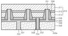
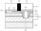
도 1a는 본 발명의 일 실시예에 따른 반도체 발광소자(100)의 개략적인 단면도이며, 도 2는 도 1의 Ⅱ-Ⅱ' 선단면도이다. 도 1b는 도 1a의 변형예이다.1A is a schematic cross-sectional view of a semiconductor
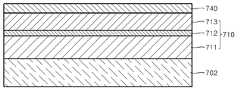
도 1a 및 도 2를 참조하면, 본 실시예의 반도체 발광소자(100)는 반도체 구조물(110)과, 반도체 구조물(110)의 일면에 마련된 전극 구조물과 전극구조물을 지지하는 기판을 포함한다.1A and 2, the semiconductor
반도체 구조물(110)은 미도시된 기판, 예컨대 사파이어 기판 상에 결정성장하여 순차적으로 형성된 제1 반도체층(111), 활성층(112), 제2 반도체층(113)을 포함한다. 사파이어 기판은 제조공정에서 제거될 수도 있으며, 도 1a에는 편의상 도시되지 않았다.The
반도체 구조물(110)은 예를 들어, GaN, InN, AlN 등과 같은 III-V족 반도체로 형성되며, 사파이어 기판은 이들 질화물 반도체와의 격자구조가 유사하여 결정성장을 위한 기판으로 사용된다. 제1 반도체층(111)은 n형 도전성을 가질 수 있으며, 제2 반도체층(113)은 p형 도전성을 가질 수 있다. 제1 반도체층(111)이 p형 도전성을 가지며, 제2 반도체층(113)이 n형 도전성을 가질 수도 있다.The
제1 반도체층(111)과 제2 반도체층(113) 사이에는 활성층(112)이 위치한다. 활성층(112)은 예를 들어, 다중양자우물구조로 형성될 수 있다. 다중양자우물구조는 다수의 양자 우물층과 이들 사이에 형성된 다수의 양자 장벽층으로 이루어진다. 구체적인 예로서, 반도체 구조물(110)이 질화갈륨계 발광 다이오드인 경우, 제1 반도체층(111)은 n형 불순물 도핑된 GaN으로 형성되고, 제2 반도체층(113)은 p형 불순물 도핑된 GaN으로 형성되며, 활성층(112)은 InGaN로 이루어진 다중 우물층과 GaN로 이루어진 양자 장벽층들이 교번적으로 적층되어 형성될 수 있다. 제1 반도체층(111)과 제2 반도체층(113)을 통해 주입된 전자 및 정공은 활성층(112)에서 결합하여 광(L)을 방출한다. 방출된 광(L)은 반도체 구조물(110)의 제1 반도체층(111)을 통해 방출된다.The
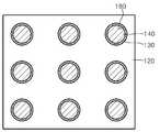
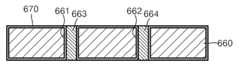
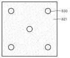
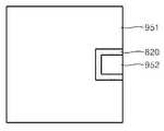
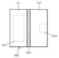
제2 반도체층(113)의 하부에는 제2전극층(120), 절연층(130), 제1전극층(140) 및 비도전성 기판(150)이 순차적으로 배치된다. 제1전극층(140)은 그 일부 영역이 절연층(130), 제2전극층(120), 제2 반도체층(113) 및 활성층(112)을 관통하고, 제1 반도체층(111)의 일정 영역까지 관통한 콘택홀(180)을 통해 연장되어 제1반도체층(111)과 접촉한다. 콘택홀(180)은 도 2에서 보듯이 복수로 형성될 수 있다. 복수의 콘택홀(180)을 채운 제1전극층(140)은 전류를 제1 반도체층(111)에 빠르게 확산시켜서 공급할 수 있다.The
콘택홀(180)은 전류 확산 및 광 추출을 고려하여 매트릭스로 배열될 수 있다. 메트릭스 배열은 도 2 또는 도 10a에서 보는 바와 같이 가로 세로 중 적어도 일방향으로 등간격을 가진 배열일 수 있다. 필요에 따라서는 간격이 서로 다른 랜덤 분포를 가질 수도 있다.The contact holes 180 may be arranged in a matrix in consideration of current spreading and light extraction. As shown in FIG. 2 or FIG. 10A, the matrix array may be an array having equal intervals in at least one of horizontal and vertical directions. If necessary, the intervals may have different random distributions.
콘택홀(180)의 크기(직경)는 0.1 ~ 500μm로 형성될 수 있으며 바람직하게는 5 ~ 300μm 일 수 있다. 본 실시예에서는 30 ~ 100μm의 콘택홀을 사용하였다.The size (diameter) of the
콘택홀(180)의 제1반도층(111)과 접촉하는 부분의 면적은 콘택홀을 포함한 제1반도체층(111)의 면적의 0.01% ~ 30%일 수 있으며, 바람직하게는 0.9% ~ 10.4%이며, 더욱 바람직하게는 대략 2.6%이다. 콘택홀(180)의 면적이 0.01% 보다 작은 경우, 동작 전압의 증가로 인하여 광효율이 감소하고 소비전력이 커질 수 있다. 반대로 콘택홀(180)의 면적이 30% 보다 클 경우, 상대적으로 발광 유효 면적이 줄어 든다. 본 실시예에서는 가로 세로 각각 1100μm크기의 정사각형 칩을 사용하였으며 제1반도층(111)과 접촉하는 콘택홀(180)의 면적이 각각 11300μm2(칩면적 대비 0.9%), 31400μm2(칩면적 대비 2.6%), 126000μm2(칩면적 대비(10.4%)인 경우의 3종류의 발광소자의 광효율을 비교하였다. 광효율은 콘택홀의 면적이 31400μm2(칩면적 대비 2.6%)인 칩이 가장 좋았으며 나머지 두개의 샘플은 10%정도 광 효율이 감소 하였다.The area of the
콘택홀(180)의 바닥의 평면(제1반도층(111))에 대한 홀의 측면 경사각(α)은 0도 보다는 크고 90도 보다는 작게 형성된다. 바람직하게는 30 ~ 60도 정도가 좋다. 경사각이 90도 이상이면 경사면에 콘택홀(180) 상에 절연막(130)의 형성이 어려울 수 있으며, 제1전극층(140)의 공정이 어려울 수 있다. 콘택홀(180)의 경사면은 광 추출 효율의 향상을 위해 계단 형상으로 형성 될 수도 있으며, 경사면에 요철이 형성 될 수도 있다. 또한 경사면 상의 일부 또는 전면에 반사 물질을 코팅 할 수도 있다. 반사 물질로는 Ag, Al, Pt, Ni, Pd, Ti, Au, Ir, W, Sn, 이들의 산화물, 또는 이들의 혼합물 중 적어도 하나를 포함해서 형성될 수 있으며 단층 혹은 복수의 층으로 형성 될 수 있다. 반사물질은 빛의 외부 추출을 향상시킨다.The lateral inclination angle α of the hole with respect to the plane of the bottom of the contact hole 180 (first semiconductor layer 111) is formed larger than 0 degrees and smaller than 90 degrees. Preferably 30 to 60 degrees is good. When the inclination angle is 90 degrees or more, it may be difficult to form the insulating
제1전극층(140) 및 제2전극층(120) 사이에는 제1전극층(140)이 제1 반도체층(111)을 제외한 다른 층과는 전기적으로 절연시키기 위한 절연층(130)이 형성되어 있다. 절연층(130)은 제1전극층(140)과 제2전극층(120)의 사이뿐만 아니라 콘택홀(180)에 의해 노출되는 제2전극층(120), 제2 반도체층(113) 및 활성층(112)의 측면들과 제1전극층(140) 사이에도 형성된다. 또한, 콘택홀(180)이 관통한 제1 반도체층(111)의 일정 영역의 측면에도 절연층(130)이 형성될 수 있다.An insulating
제2전극층(120)은 제2 반도체층(113)과 접촉되게 형성된다. 제2전극층(120)이 제2 반도체층(113)과 전기적으로 접촉하기 때문에 제2 반도체층(113)과의 접촉 저항을 최소화하면서도 활성층(112)에서 생성된 광을 반사시켜 외부로 향하게 하여 발광 효율을 높일 수 있는 반사기능을 가지는 물질로 형성된다. 제2전극층(120)은 Ag, Al, Pt, Ni, Pd, Ti, Au, Ir, W, Sn, 이들의 산화물 또는 이들의 혼합물로 구성된 물질을 적어도 하나 포함해서 형성될 수 있으며 단층 혹은 복수의 층으로 형성 될 수 있다. 각 층의 두께는 각각 0.1 ~ 5000nm로 형성될 수 있다. 바람직하게는 2 ~ 2000nm이다. 본 실시예에서는 제2전극층(120)은 Ag/Ni/Ti/TiN의 4층 구조를 사용하였으며 각각은 150nm/50nm/50nm/400nm의 두께로 증착하였다. 제2전극층(120)의 Ag(150nm)층의 두께는 40nm 보다 얇으면 반사도가 떨어져 광출력이 감소하며 150nm 보다 두꺼우면 재료비 및 공정시간이 증가하므로 100 ~ 150nm범위가 적절하다. 제2전극층(120) 형성후 오믹콘택 형성을 위해 열처리를 행한다. 본 실시예에서는 열처리로 RTA법을 사용하여 350℃에서 60초간 실시하여 양호한 오믹 특성을 얻었다. 열처리의 온도 및 시간은 오믹 전극의 재료에 따라 다르지만 300 ~ 800℃에서 5 ~ 5000초정도 행해질 수 있다. 적절하게는 300 ~ 600℃에서 30 ~ 180초가 좋다.The
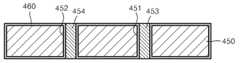
비도전성 기판(150)에는 제1전극층(140)에 전류를 공급하는 제1콘택(153)이 채워진 제1 관통홀(151)과, 제2전극층(120)에 전류를 공급하는 제2콘택(154)이 채워진 제2 관통홀(152)이 형성되어 있다. 제2 관통홀(152)은 연장되어서 제1전극층(140)을 관통한다. 제2 관통홀(152)의 내주에는 제2콘택(154)을 제1전극층(140)과 전기적으로 분리시키는 절연층(156)이 더 형성된다. 제1콘택 (153)은 비도전성기판(150)을 관통하여 제1전극층(140)에 전기적으로 접속된다. 제2콘택(154)은 비도전성기판(150), 제1전극층(140) 및 절연층(130)을 관통하여 제2전극층(120)에 전기적으로 접속된다.The
비도전성 기판(150)은 질화물계(GaN, AlN, AlGaN, InGaN 등), 알루미늄 산화물계(사파이어, 알루미나 등), 다이아몬드, 실리콘계(Si 등), Ga산화물계(Ga2O3, LiGaO2 등), Zn산화물계(ZnO 등), 세라믹, 폴리머 중 어느 하나의 물질을 포함할 수 있다.The
상기 실시예에서는 비도전성 기판(150)에 제1콘택(153) 및 제2콘택(154)이 형성되는 것을 기재하고 있지만, 본 발명은 반드시 이에 한정되는 것은 아니다. 예컨대, 도전성 기판(도 4b 참조)에 관통홀을 형성하고 관통홀의 내주 및 도전성 기판의 표면에 절연층(도 4b의 460)을 형성하고, 그 내부에 메탈을 채워서 제1콘택(도 4b의 452)과 제2콘택(도 4b의 454)을 형성한 구조를 가질 수도 있으며, 이에 대한 상세한 구조는 후술되는 도 4a-4c의 실시예를 참조한다. 도전성 기판은 Si계, Ge계, 알루미늄 포함 Si 물질계, 질화물계(GaN 등)로 형성될 수 있다.In the above embodiment, the
본 발명의 실시예에 따른 반도체 발광소자는 전술한 바와 같이, 제1 반도체층과 제2 반도체층에 연결된 전극을 발광소자의 하부면에 형성함으로써, 발광면적의 손실이 감소되게 전극을 형성하므로 발광효율을 극대화할 수 있다. 또한, 전극이 발광소자의 비도전성 기판의 하부면에 형성되므로, 와이어 본딩없이 직접 패키지 다이본딩을 할 수 있다.In the semiconductor light emitting device according to the embodiment of the present invention, as described above, by forming electrodes connected to the first semiconductor layer and the second semiconductor layer on the lower surface of the light emitting device, the electrode is formed so that the loss of the light emitting area is reduced, The efficiency can be maximized. In addition, since the electrode is formed on the lower surface of the non-conductive substrate of the light emitting device, package die bonding can be performed directly without wire bonding.
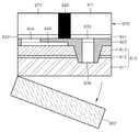
도 1b는 도 1a의 변형예인 발광소자(100')를 개략적으로 도시한 단면도이며, 도 1a의 구성요소와 실질적으로 동일한 구성요소에는 동일한 참조번호를 사용하고 상세한 설명은 생략한다.FIG. 1B is a cross-sectional view schematically illustrating a
도 1b를 참조하면, 발광소자(100')는 반도체 구조물(110)의 제1 반도체층(111) 상에 사파이어 기판(102)이 배치된다. 사파이어 기판(102)은 반도체 구조물(110)의 성장 기판이다. 사파이어 기판(102)의 표면에는 요철부가 형성될 수 있다. 요철부는 발광소자(100')의 광추출 효율을 증가시킬 수 있다. 발광소자(100')의 다른 구성요소는 발광소자(100)와 실질적으로 동일하므로, 상세한 설명은 생략한다.Referring to FIG. 1B, in the
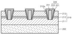
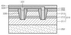
도 3a 내지 도 3j는 본 발명의 다른 실시예에 따른 반도체 발광소자의 제조방법을 설명하기 위한 단면도이다. 도 3a 내지 도 3j는 설명의 편의를 위하여 하나의 발광소자를 제조하는 공정을 도시하였으나, 실제로는 복수의 발광소자를 웨이퍼 상에 일체로 형성한 후 각각 절단하여 개별 발광소자로 하거나, 복수의 발광소자를 일체로 형성한 발광소자를 제조할 수 있다.3A to 3J are cross-sectional views illustrating a method of manufacturing a semiconductor light emitting device according to another embodiment of the present invention. 3A to 3J illustrate a process of manufacturing one light emitting device for convenience of description, in practice, a plurality of light emitting devices are integrally formed on a wafer and then cut into individual light emitting devices or a plurality of light emitting devices. A light emitting device in which the devices are integrally formed can be manufactured.
도 3a를 참조하면, 기판(202)의 상면에 제1 반도체층(211), 활성층(212) 및 제2 반도체층(213)을 순차적으로 결정성장시켜 반도체 구조물(210)을 형성한다.Referring to FIG. 3A, the
기판(202)은 결정성장시키고자 하는 반도체에 적합한 것을 선택할 수 있다. 예를 들어, 질화물 반도체 단결정을 성장시키는 경우, 기판(202)은 사파이어 기판, ZnO 기판, GaN 기판, SiC 기판, AlN 기판 등에서 선택할 수 있다.The
기판(202)은 사이즈에 따라 대략 300 ~ 1200μm의 두께를 가진다. 기판(202)은 상면에 결정 성장 시키는 물질의 종류(열팽창 계수 차)에 따라 기판(202)의 표면 또는 배면에 여러 형태의 패턴을 형성 할 수도 있다. 상기 패턴들은 결정 성장시의 결정 결함을 줄이는 역할도 하고 동시에 열 팽창 등에 의한 스트레스 완화의 역할도 한다. 상기 패턴들에 의해 광의 외부 추출 효율을 증가시키는 역할도 할 수 있다. 패턴의 형상들은 평면상으로 원형 또는 다각형(삼각형, 사각형, 오각형, 육각형, 팔각형등)으로 형성될 수 있고 단면 형상으로는 반구형, 원뿔, 또는 다각형(삼각형, 사다리꼴등의 사각형, 오각형, 육각형 등) 등으로 형성 될 수 있다. 기판(202)은 결정 성장 후에 레이저빔 또는 화학적 에칭등에 의해 전체 또는 일부가 제거 될 수도 있고 또는 두께를 50 ~ 300μm정도로 얇게 할 수도 있으며, 표면에 요철 패턴을 형성 할 수도 있다.The
도 3a에는 도시되지 않았지만, 기판(202)과 제1 반도체층(211)의 사이에는 버퍼층(미도시)이 더 형성될 수 있다. 버퍼층은 성장된 제1 반도체층(211)과 기판(202)의 격자정합을 향상시키기 위한 층으로, 예를 들어, 질화물 반도체 단결정을 성장시키는 경우, SiC, 질화물(GaN, AlGaN, InGaN, InN, AlInGaN 등), Zn산화물, Si산화물 또는 이들의 조합으로 이루어진 물질 중 하나를 포함하여 형성될 수 있다.Although not shown in FIG. 3A, a buffer layer (not shown) may be further formed between the
버퍼층은 400 ~ 800℃에서 2 ~ 800nm두께로 단일층 혹은 다층으로 형성할 수 있으며 비정질 또는 다결정 또는 이들의 혼합물로 형성된다. 버퍼층의 상면에는 단결정의 반도체층이 형성된다. 예들 들어 500 ~ 600℃에서 비정질 또는 다결정의 혼합물 GaN버퍼층을 형성하고 그 다음에 1000 ~ 1200℃에서 단결정의 GaN층을 형성한다. 이 과정에서 상기 비정질 또는 다결정의 혼합물 GaN버퍼층의 적어도 일부가 단결정화 된다.반도체 구조물(210)은 예를 들어, GaN, InN, AlN 등과 같은 III-V족 반도체를 결정성장시켜 형성할 수 있다. 일례로, 반도체 구조물(210)이 질화갈륨계 발광 다이오드인 경우, 제1 반도체층(211), 활성층(212) 및 제2 반도체층(213)은 AlxInyGa(1-x-y)N 조성식 (여기서, 0≤x≤1, 0≤y≤1, 0≤x+y≤1)을 갖는 반도체 물질일 수 있으며, 유기금속 화학기상증착(Metal Organic Chemical Vapor Deposition, MOCVD) 설비를 이용한 에피택셜(Epitaxial) 성장방법 등으로 형성될 수 있다. 즉, 제1 반도체층(211)은 Si, Ge, Sn과 같은 제1 도전형 불순물이 도핑되거나 또는 논도핑 또는 이들의 조합으로 된 질화물 반도체층(GaN, InN, InGaN, AlGaN, AlN, AlInGaN 또는 이들의 조합)으로 형성될 수 있다. 활성층(212)은 다중 양자우물(Multi-Quantum Well)구조(InGaN/GaN층, InGaN/InGaN층, AlGaN/GaN층, AlGaN/AlGaN층, AlInGaN/AlInGaN층 또는 이들의 조합)으로 형성되거나, 하나의 양자우물층 또는 더블 헤테로 구조로도 형성될 수 있다. 제2 반도체층(213)은 Mg, Zn, Be과 같은 제2 도전형 불순물이 도핑되거나 혹은 논도핑 또는 이들의 조합으로된 질화물 반도체층(GaN, InN, InGaN, AlGaN, AlN, AlInGaN 또는 이들의 조합)으로 형성될 수 있다. 제1 반도체층(211), 활성층(212), 제2 반도체층(213)은 각 층의 역할에 따라 다양한 두께(1nm ~ 10000nm) 또는 불순물 농도(1x10¹⁵/cm3 ~ 1x10²²/cm3)를 가질 수 있다.The buffer layer may be formed in a single layer or multiple layers at a thickness of 2 to 800 nm at 400 to 800 ° C., and may be formed of amorphous or polycrystalline or a mixture thereof. A single crystal semiconductor layer is formed on the upper surface of the buffer layer. For example, a mixed GaN buffer layer of amorphous or polycrystal is formed at 500 to 600 ° C, followed by a single crystal GaN layer at 1000 to 1200 ° C. In this process, at least a portion of the amorphous or polycrystalline GaN buffer layer is monocrystalline. The
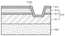
도 3b를 참조하면, 제2 반도체층(213)으로부터 소정 깊이(0.5 ~ 20μm)로 건식 에칭(ICP-RIE 방법 등) 및/또는 습식 에칭을 이용하여 제1 반도체층(211)의 일부 깊이까지 에칭한 콘택홀(210a)을 형성한다. 콘택홀(210a)의 에칭의 깊이는 적어도 제1 반도체층(211)의 표면이 노출되도록 제2 반도체층(213) 및 활성층(212)을 제거한다. 제1 반도체층(211)의 일부도 소정 깊이(0.1nm ~ 5000nm)로 에칭할 수 있으며, 필요에 따라서는 관통홀을 형성 할 수도 있다. 콘택홀(210a)의 크기(직경)는 0.1μm ~ 500μm로 형성될 수 있으며 바람직하게는 5μm ~ 300μm가 적당하다. 콘택홀(210a)은 복수로 형성 될 수 있으며, 제1 반도층(211)과 접촉하는 부분의 콘택홀(210a)의 면적은 콘택홀(210a)을 포함한 제1 반도체층(211)의 면적 대비 0.01% ~ 30%일 수 있으며, 바람직하게는 0.9% ~ 10.4%이며, 더욱 바람직하게는 대략 2.6%이다. 콘택홀(210a) 바닥의 평면(제1 반도층(211))에 대한 콘택홀(210a)의 측면 경사각(α)은 0도 보다는 크고 90도 보다는 작게 형성한다. 바람직하게는 30 ~ 60도 정도가 좋다. 경사각이 90도 보다 크면 경사면에 절연막(221)의 형성이 어렵고 후술되는 제1전극층의 형성이 어려울 수 있다. 콘택홀(210a)의 경사면은 광 추출 효율의 향상을 위해 계단 형상으로 형성 될 수도 있으며 경사면에 요철이 형성 될 수도 있다. 또한 경사면 상의 일부 또는 전면에 반사 물질을 코팅 할 수도 있다. 반사 물질로는 Ag, Al, Pt, Ni, Pd, Ti, Au, Ir, W, Sn, 이들의 산화물, 또는 이들의 혼합물 중 적어도 하나를 포함해서 형성될 수 있으며, 단층 혹은 복수의 층으로 형성 될 수 있다. 반사물질은 빛의 외부 추출을 향상시킨다.Referring to FIG. 3B, from the
콘택홀(210a)을 포함하는 반도체 구조물(210)의 상부면 전역에 절연층(221)을 증착방법을 이용하여 도포한다. 예를 들어, 절연층(221)은 플라즈마 화학증착(Plasma Enhanced Chemical Vapor Deposition, PECVD)을 이용하여 SiO2또는 SiNx 를 증착하여 형성할 수 있다. 절연층(221)은 0.001 ~ 50μm 두께로 형성될 수 있다. 바람직하게는 0.3 ~ 1.2μm 두께로 형성된다.도 3c를 참조하면, 절연층(221) 중에서 콘택홀(210a)의 바닥에 형성된 부분을 식각하여 제1 반도체층(211)을 노출시킨다. 이러한 식각은 예를 들어, RIE(Reactive Ion Etching) 건식 식각 또는 BOE(Buffered Oxide Echant)를 이용한 습식 식각방법으로 이루어질 수 있다.The insulating
제1 반도체층(211)의 노출된 영역에 콘택층(231)을 형성한다. 콘택층(231)은 제1 반도체층(211)과 오믹 콘택을 형성할 수 있는 물질로 형성하되 반사도가 우수한 물질이 좋다. 예들 들면 Al, Ti, Pt, Ag, Ni, TiN, Au, Sn, 및 이들 혼합물 중의 적어도 하나를 포함하는 물질로 이루어진 단층 혹은 서로 다른 복수의 층으로 구성 될 수 있다. 각 층의 두께는 각각 0.1 ~ 5000nm로 구성 될 수 있다. 예를 들어, 본 실시에서는 Al/Ti/Pt/Ti층을 200nm/300nm/100nm/2nm의 두께로 증착하여 형성하였다. 이때, 콘택층(231)은 도 2 또는 도 10a에 도시된 것과 같이 복수개로 형성하여, 제1 반도체층(211)으로의 전류 확산(current spreading)을 향상시킨다. 복수개의 콘택층(231)은 매트릭스 형태로 배열될 수 있다. 콘택층(231) 형성후에는 오믹 콘택 형성을 위한 열처리를 행한다. 본 실시예에서 열처리는 RTA(rapid thermal annealing)법으로 550도에서 60초간 실시 하여 양호한 오믹 특성을 얻었다. 열처리의 온도 및 시간은 오믹 전극의 재료에 따라 다르지만 300 ~ 800도에서 5 ~ 5000초 정도에서 행해 질 수 있다. 적절하게는 300 ~ 600도에서 30 ~ 180초가 좋다.The
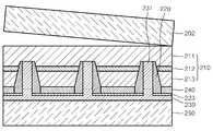
제2 반도체층(213) 상으로 절연층(222)을 형성하여, 콘택홀(210a)에서 절연층(221) 및 콘택층(231) 사이를 절연층(222)을 채운다. 절연층(222)은 절연층(221)과 동일한 물질로 형성될 수 있다.The insulating
도 3d를 참조하면, 콘택홀(210a)을 둘러싼 영역을 제외한 나머지 영역의 절연층(221, 222)을 식각하여, 제2 반도체층(213)을 노출시킨다. RIE 건식식각 또는 BOE를 이용한 습식식각을 사용할 수 있다.Referring to FIG. 3D, the insulating
이하에서는 절연층(221) 및 절연층(222)을 합친 절연층을 편의상 절연층(220)으로도 칭한다.Hereinafter, the insulating layer in which the insulating
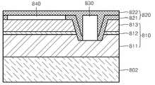
도 3e를 참조하면, 노출된 제2 반도체층(213) 상에 제2전극층(240)을 형성한다. 제2전극층(240)은 오믹특성과 광반사특성을 동시에 지닌 금속으로 형성하여 반사막의 역할을 하거나, 또는 오믹특성과 광반사특성을 각각 지닌 금속이 순차 적층되어 이루어진 다중층으로 형성할 수 있다. 제2전극층(240)은 Ag, Al, Pt, Ni, Pd, Ti, Au, Ir, W, Sn, 이들의 산화물, 또는 이들의 혼합물 중 적어도 하나를 포함해서 형성될 수 있으며 단층 혹은 복수의 층으로 형성 될 수 있다. 이들 물질은 빛의 외부 추출을 향상 시킨다.Referring to FIG. 3E, a
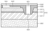
제2전극층(240) 상에 소정 두께로 절연층(223)을 형성한다. 절연층(223)은 예를 들어, PECVD를 이용하여 SiO2를 증착하여 형성할 수 있다. 도 3f를 참조하면, 절연층(220)을 식각하여 콘택층(231)을 노출시킨다. 절연층(220) 상으로 금속물질을 도포하여 노출된 콘택층(231)과 연결되는 제1전극층(230)을 형성한다. 제1전극층(230)은 Ti(100nm)/Ni(100nm) 구성의 층을 4번 반복 적층한 후 Ti(100nm)/Au(1500nm)/Sn(1400nm)/Au(10nm)층을 추가 적층 하였다.The insulating
도 3g를 참조하면, 제1전극층(230) 상에 비도전성 기판(250)을 본딩한다. 비도전성 기판(250)으로는 알루미나 기판, AlN 기판, 사파이어 기판, 세라믹 기판, 폴리머 기판 등을 사용할 수 있다. 비도전성 기판(250)을 제1전극층(230) 상에 접합하기 위해서 그들 사이에 도전성 접착물질 또는 비도전성 접착물질을 매개체로 사용할 수 있다. 도전성 접착물질로는 AuSn, Au, Cu, Pb, W, Ti, Pt, Sn, TiSn 또는 이들의 혼합물 중 적어도 하나를 포함하는 물질의 단층 또는 다층으로 사용될 수 있다. 비도전성 접착물질로는 SOG, 폴리머 등이 사용될 수 있다.Referring to FIG. 3G, the
도 3h를 참조하면, 제1 반도체층(211)으로부터 기판(202)을 제거한다. 예컨대 기판(202) 상으로 레이저 광을 조사하여 기판(202)과 제1 반도체층(211) 사이에서 열적 반응을 일으켜서 재료분리가 일어나게 한다. 기판(202)을 제1 반도체층(211)으로부터 리프트오프하여 제거한다. 기판(202)를 화학적 에칭 또는 화학기계적 연마 방법(Chemical-mechanical polishing)을 수행하여 제거할 수도 있다.Referring to FIG. 3H, the
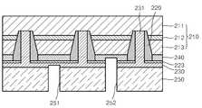
도 3i를 참조하면, 비도전성 기판(250)의 노출된 표면으로부터 제1전극층(230)과 제2전극층(240)과 각각 연결된 제1관통홀(251) 및 제2관통홀(252)을 형성한다. 기판(250)의 두께는 50 ~ 300μm가 될 수 있고 적당하게는 100 ~ 200μm가 좋다. 너무 두꺼우면 콘택홀(251, 252) 형성에 시간이 걸리는 등의 공정상 문제점이 있으며 너무 얇어도 지지기판으로의 역할을 충분히 할 수 없다.Referring to FIG. 3I, a first through
관통홀(251, 252)의 크기(직경)는 0.1μm ~ 500μm로 형성될 수 있으며 바람직하게는 5μm ~ 300μm가 적당하다. 각 관통홀(251, 252)은 단수 혹은 복수로 형성 될 수 있다. 관통홀(251, 252)의 면적은 대략 기판(250)의 바닥면(250a)의 0.01% ~ 30%일 수 있다. 관통홀(251, 252)은 바닥면(250a)을 기준으로 계단 형상 또는 테이퍼 형상으로 경사지게 형성할 수 있다.도 3j를 참조하면, 제2 관통홀(252)의 측면에는 절연층(256)을 형성한다. 이때, 제1 관통홀(251)의 측면에도 절연층(미도시)이 절연층(256)과 함께 형성될 수 있다. 제1관통홀(251)과 제2관통홀(252)에 각각 메탈로 이루어진 제1콘택(253)과 제2콘택(254)을 형성한다. 제1관통홀(251)과 제2관통홀(252)은 레이저 드릴링, 건식식각 방법, 또는 습식식각 방법을 사용하여 형성할 수 있다.The size (diameter) of the through
도 4a 내지 도 4c는 본 발명의 또 다른 실시예에 따른 반도체 발광소자의 제조방법을 설명하기 위한 단면도이다.4A to 4C are cross-sectional views illustrating a method of manufacturing a semiconductor light emitting device according to still another embodiment of the present invention.
도 3a-3f의 공정은 동일하게 수행될 수 있으며, 상세한 설명은 생략한다.The process of FIGS. 3A-3F may be performed in the same manner, and detailed description thereof will be omitted.
도 4a를 참조하면, 도 3a-3f의 공정에 의한 결과물에서, 제1전극층(230)의 노출된 표면으로부터 제2전극층(240)과 연결된 관통홀(441)을 형성한다. 관통홀(441)의 측면에는 절연층(442)를 형성한다. 관통홀(441)에 메탈로 이루어진 콘택(443)을 형성한다. 관통홀(441)은 레이저 드릴링, 건식식각 방법 등을 사용하여 형성할 수 있다. 제1전극층(230)의 두께는 0.1μm ~ 300μm가 될 수 있으며, 적당하게는 0.5 - 100μm가 좋다. 300μm보다 두꺼우면 관통홀(441) 형성에 있어 시간이 걸리며 비용이 증가하는 등의 공정상 문제점이 있으며 0.1μm보다 얇으면 접합층으로의 역할을 충분히 할 수 없다. 관통홀(441)의 크기(직경)는 0.1 - 500μm로 형성될 수 있으며 바람직하게는 5 - 300μm가 적당하다. 본 발명에서는 30 - 100μm 크기로 관통홀(441)을 형성하였다. 관통홀(441)은 단수 혹은 복수로 형성 될 수 있다. 관통홀(441)의 면적은 제1전극층(230)의 면적 대비 0.01% - 30%일 수 있다. 관통홀(441)은 제1 전극층(230)의 상면(230a)을 기준으로 계단 형상 또는 테이퍼 형상으로 경사지게 형성할 수 있다.Referring to FIG. 4A, in the result of the process of FIGS. 3A-3F, a through
절연층(442)은 0.001 - 50μm 두께로 형성될 수 있으며, 관통홀(441)의 직경대비 절연층(442)의 두께는 0.01% - 30% 정도가 적당하다. 본발명에서 절연층(442)의 두께는 0.01 - 0.9μm 범위로 형성하였다.The insulating
도 4b를 참조하면, 도전성 기판(450)에 제1 관통홀(451)과 제2 관통홀(452)을 형성한다. 제2 관통홀(452)은 관통홀(441)과 대응되게 형성하며, 제1 관통홀(451)는 제2 관통홀(452)과 이격되게 형성한다. 도전성 기판은 Si, Ge, 금속 포함 실리콘(예컨대 Al 포함 실리콘)으로 형성될 수 있다.Referring to FIG. 4B, a first through
도전성 기판(450)에서 제1 관통홀(451)과 제2 관통홀(452)의 내주면을 포함하는 표면에 절연층(460)을 형성한다.The insulating
제1 관통홀(451)과 제2 관통홀(452)를 메탈로 채워서 각각 제1 콘택(453)과 제2 콘택(454)을 형성한다.The first through
도 4c를 참조하면, 도전성 기판(450)의 제2 콘택(454)이 콘택(443)과 접촉되게 도전성 기판(450)을 제1전극층(230) 상에 본딩한다. 도전성 기판(450)을 제1전극층(230) 상에 접합하기 위해서 제1 콘택(453) 및 제2 콘택(454) 상에 도전성 접착물질(미도시)을 형성하고, 다른 부분에 비도전성 접착물질(미도시)을 매개체로 사용할 수 있다. 도전성 접착물질로는 AuSn, Au, Cu, Pb, W, Ti, Pt, Sn, TiSn 또는 이들의 혼합물 중 적어도 한 종류의 물질을 포함하며, 단층 또는 복층으로 형성될 수 있다. 비도전성 접착물질로는 SOG, 폴리머 등이 사용될 수 있다.Referring to FIG. 4C, the
제1 반도체층(211)으로부터 기판(202)을 제거한다. 예컨대 기판(202) 상으로 레이저 광을 조사하여 기판(202)과 제1 반도체층(211) 사이에서 열적 반응을 일으켜서 재료분리가 일어나게 한다. 기판(202)을 제1 반도체층(211)으로부터 리프트오프하여 제거한다. 기판(202)을 화학적 에칭 또는 화학기계적 연마 방법(Chemical-mechanical polishing)을 수행하여 제거할 수도 있다. 기판(202)의 두께를 얇게하거나 기판(202) 표면에 요철을 형성하여 기판(202)을 제거하지 않고 사용할 수도 있다.The
도 4a-4c의 제조방법에서는 도전성 기판(450)을 사용하였으나, 비도전성 기판(250)을 사용하는 방법에도 적용할 수 있으며, 상세한 설명은 생략한다.Although the
도 5는 다른 실시예에 따른 반도체 발광소자(500)의 개략적인 단면도이다.5 is a schematic cross-sectional view of a semiconductor
도 5를 참조하면, 본 실시예의 반도체 발광소자(500)는 반도체 구조물(510)과, 반도체 구조물(510)의 일면에 마련된 전극 구조물과 전극구조물을 지지하는 기판(560)을 포함한다.Referring to FIG. 5, the semiconductor
반도체 구조물(510)은 미도시된 기판, 예컨대 사파이어 기판 상에 결정성장하여 순차적으로 형성된 제1 반도체층(511), 활성층(512), 제2 반도체층(513)을 포함한다. 사파이어 기판은 제조공정에서 제거되므로, 도 5에는 도시되지 않았다.The
반도체 구조물(510)은 예를 들어, 질화갈륨계(GaN, InN, InGaN, AlGaN, AlN, AlInGaN 또는 이들의 조합)와 같은 III-V족 반도체로 형성되며, 사파이어 기판은 이들 질화물 반도체와의 격자구조가 유사하여 결정성장을 위한 기판으로 사용된다. 제1 반도체층(511)은 n형 도전성을 가질 수 있으며, 제2 반도체층(513)은 p형 도전성을 가질 수 있다. 또는, 제1 반도체층(511)이 p형 도전성을 가지며, 제2 반도체층(513)이 n형 도전성을 가질 수도 있다.The
제1 반도체층(511)과 제2 반도체층(513) 사이에는 활성층(512)이 위치한다. 활성층(512)은 예를 들어, 단일 또는 다중양자우물구조로 형성될 수 있다. 제1 반도체층(511)과 제2 반도체층(513)을 통해 주입된 전자 및 정공은 활성층(512)에서 결합하여 광(L)을 방출한다. 방출된 광(L)은 반도체 구조물(510)의 제1 반도체층(511)을 통해 방출된다.An
제2 반도체층(513)의 하부에는 제2전극층(520), 절연층(530), 제1전극층(540) 및 기판(560)이 순차적으로 배치된다. 제1전극층(540)은 그 일부 영역이 절연층(530), 제2전극층(520), 제2 반도체층(513) 및 활성층(512)을 관통하고, 제1 반도체층(511)의 일정 영역까지 관통한 콘택홀(580)을 통해 연장되어 제1반도체층(511)과 접촉한다. 콘택홀(580)은 복수로 형성될 수 있다(도 2 참조). 복수의 콘택홀(580)을 채운 제1전극층(540)은 전류를 제1 반도체층(511)에 빠르게 확산시켜서 공급할 수 있다.The
콘택홀(580)의 에칭의 깊이는 적어도 제1 반도체층(511)의 표면이 노출되도록 제2 반도체층(513) 및 활성층(512)을 제거한다. 제1 반도체층(511)의 일부도 소정 깊이(0.1nm ~ 5000nm)로 에칭할 수 있으며, 필요에 따라서는 관통홀을 형성 할 수도 있다. 콘택홀(580)의 크기(직경)는 0.1μm ~ 500μm로 형성될 수 있으며 바람직하게는 5μm ~ 300μm가 적당하다. 콘택홀(580)은 복수로 형성 될 수 있으며, 제1 반도층(211)과 접촉하는 부분의 콘택홀(580)의 면적은 콘택홀(580)을 포함한 제1 반도체층(211)의 면적 대비 0.01% ~ 30%일 수 있으며, 바람직하게는 0.9% ~ 10.4%이며, 더욱 바람직하게는 대략 2.6%이다. 콘택홀(580)의 바닥에는 요철이 형성될 수 있다. 콘택홀(580) 바닥의 평면(제1 반도층(511))에 대한 콘택홀(580)의 측면 경사각(α)은 0도 보다는 크고 90도 보다는 작게 형성한다. 바람직하게는 30 ~ 60도 정도가 좋다. 경사각이 90도 보다 크면 경사면에 절연막(530)의 형성이 어렵고 제1전극층(540)의 형성이 어려울 수 있다. 콘택홀(580)의 경사면은 광 추출 효율의 향상을 위해 계단 형상으로 형성 될 수도 있으며 경사면에 요철이 형성 될 수도 있다. 또한 경사면 상의 일부 또는 전면에 반사 물질을 코팅 할 수도 있다. 반사 물질로는 Ag, Al, Pt, Ni, Pd, Ti, Au, Ir, W, Sn, 이들의 산화물, 또는 이들의 혼합물 중 적어도 하나를 포함해서 형성될 수 있으며, 단층 혹은 복수의 층으로 형성 될 수 있다. 반사물질은 빛의 외부 추출을 향상시킨다.The depth of etching of the
제1전극층(540) 및 제2전극층(520) 사이에는 제1전극층(540)이 제1 반도체층(511)을 제외한 다른 층과는 전기적으로 절연시키기 위한 절연층(530)이 형성되어 있다. 절연층(530)은 제1전극층(540)과 제2전극층(520)의 사이뿐만 아니라 콘택홀(580)에 의해 노출되는 제2전극층(520), 제2 반도체층(513) 및 활성층(512)의 측면들과 제1전극층(540) 사이에도 형성된다. 또한, 콘택홀(580)이 관통한 제1 반도체층(511)의 일정 영역의 측면에도 절연층(530)이 형성될 수 있다. 절연층(530)은 0.001 ~ 50μm 두께로 형성 될 수 있으며, 콘택홀(580)의 직경대비 절연층(530)의 두께는 0.001% ~ 30% 정도가 적당하다. 본발명에서 절연층(530)의 두께는 0.01 ~ 0.9μm 범위로 형성하였다.An insulating
제2전극층(520)은 제2 반도체층(513)과 접촉되게 형성된다. 콘택홀(580)이 관통하는 일정 영역들에는 제2전극층(540)이 존재하지 않는다. 제2전극층(520)이 제2 반도체층(513)과 전기적으로 접촉하기 때문에 제2 반도체층(513)과의 접촉 저항을 최소화하면서도 활성층(512)에서 생성된 광을 반사시켜 외부로 향하게 하여 발광 효율을 높일 수 있는 반사기능을 가지는 물질로 형성될 수 있다. 제2전극층(520)은 Ag, Al, Pt, Ni, Pd, Ti, Au, Ir, W, Sn, 이들의 산화물 또는 이들의 혼합물로 구성된 물질 중 적어도 하나를 포함해서 형성될 수 있다.The
제1전극층(540)의 일부 영역의 하부에는 제1 전극패드(551)가 형성되어 있다. 제1전극층(540)에서 제1 전극패드(551)에 접하지 않은 영역에는 절연층(534)이 형성되어 있다. 절연층(534)은 절연층(530)과 접한다.The
제2전극층(520)의 하부에서 절연층(530)이 형성되지 않은 영역에는 제2전극패드(552)가 형성되어 있다. 제2 전극패드(552)는 제2전극층(520)과 전기적으로 접속한다. 제2 전극패드(552)는 공간(554)에 의해 제1전극패드(551)과 이격된다. 제2 전극패드(552)는 제1 전극패드(551)과 이격되면서 수직위치에서 동일한 위치로 형성될 수 있다. 제2 전극패드(552)와 제1 전극패드(551)는 필요에 따라서 차지하는 면적을 설계할 수 있다.The
전극패드(551, 552)로는 AuSn, Au, Al, Ni, Cu, Pb, W, Ti, Pt, Sn, TiSn 또는 이들의 혼합물 중 적어도 하나를 포함하는 물질로 형성될 수 있다. 전극패드(551, 552)는 단층 또는 서로 다른 물질의 층의 복수의 층으로 형성될 수 있다. 전극패드(551, 552)의 두께는 0.1 ~ 500μm일 수 있다. 제1 전극패드(551)가 제2 전극패드(552)보다 크거나 동일한 면적으로 형성되는 방열 등을 고려할 때 바람직하다.The
공간(554)은 절연물질(미도시)로 채워질 수도 있다.The
제1 전극패드(551) 및 제2 전극패드(552)의 하부에는 기판(560)이 부착된다. 기판(560)에는 이격된 제1 관통홀(561) 및 제2 관통홀(562)이 형성되어 있다. 제1 관통홀(561) 및 제2 관통홀(562)에는 각각 제1콘택(563)과 제2콘택(564)이 형성되어 있다. 제1콘택(563)과 제2콘택(564)는 각각 제1 전극패드(551)와 제2 전극패드(552)와 연결된다. 기판(560)이 도전성 기판인 경우, 기판(560)을 콘택(563, 564) 및 전극패드(551, 552)와 절연하도록 절연층(570)이 더 형성된다.The
반도체 발광소자(500)는 콘택(564)과 접촉하는 제2 전극패드(552)의 영역이 넓게 형성되어서, 용이하게 기판(560)을 전극패드에 본딩할 수 있다. 또한, 콘택이 형성된 기판과의 접속을 위해서 용이하게 전극패드(551, 552)의 위치 및 면적을 변경할 수 있다. 제2 전극패드(552)와 제2콘택(564)의 접촉을 용이하게 하기 위해 제2전극패드(552)의 면적은 제2콘택(564)의 면적보다 최소 1.2배 이상이 되게 형성한다. 제1전극패드(551) 및 제1콘택(563)도 마찬가지로 상호 접촉을 용이하게 하기 위해 제1전극패드(551)의 면적이 제1콘택(563)의 면적보다 최소 1.2배 이상으로 하는 것이 좋다.The semiconductor
도 6a 내지 도 6g는 본 발명의 다른 실시예에 따른 반도체 발광소자의 제조방법을 설명하기 위한 도면이다. 도 3a 내지 도 3e의 공정은 동일하게 수행될 수 있으며, 동일한 부재에 대해 동일한 참조번호를 사용항고 상세한 설명은 생략한다.6A to 6G illustrate a method of manufacturing a semiconductor light emitting device according to another exemplary embodiment of the present invention. 3A to 3E may be performed in the same manner, the same reference numerals are used for the same members, and detailed description thereof will be omitted.
도 6a에는 편의상 2개의 콘택층(231)을 도시하였다. 도 6a를 참조하면, 절연층(223)을 식각하여 콘택층(231)을 노출시킨다. 절연층(223) 상에서 제2전극층(240)의 제1영역(A1) 상으로 포토레지스트(632)를 형성하고, 포토레지스트(632)에 노출된 제2영역(A2)에 금속물질을 도포하여 노출된 콘택층(231)과 연결되는 제1전극층(630)을 형성한다.6A shows two
도 6b를 참조하면, 포토레지스트(632)를 제거한 후, 절연층(223) 위로 제1전극층(630)을 덮는 절연층(634)를 형성한다.Referring to FIG. 6B, after removing the
도 6c를 참조하면, 제1영역(A1)의 절연층(634, 223)을 패터닝하여 제2전극층(240)을 노출시킨 후, 노출된 제2전극층(240)과 연결된 제2 전극패드(652)를 형성한다. 제2 전극패드(652)는 제2영역(A2)의 일부 절연층(634)을 덮도록 형성하여 제2 전극패드(652) 형성영역을 증가시킨다.Referring to FIG. 6C, after patterning the insulating
도 6d를 참조하면, 제2영역(A2)의 절연층(634) 일부를 식각하여 제2 전극패드(652)와 이격되게 제1전극층(630)을 노출시킨 후, 노출된 제1전극층(630) 위로 제1 전극패드(651)를 형성한다. 제1 전극패드(651)의 표면과 제2 전극패드(652)의 표면이 수평으로 형성될 수 있다.Referring to FIG. 6D, a portion of the insulating
도 6e는 도 6d의 결과물의 평면도이다. 도 6e를 참조하면, 제1 전극패드(651)와 제2 전극패드(652)는 서로 이격된다. 제1 전극패드(651) 및 제2 전극패드(652)는 제1전극층(630) 및 제2전극층(240)의 면적과 관계없이 용이하게 설계할 수 있다. 따라서, 후술하는 미리 만들어진 기판에 형성된 전극과의 전기적 접속을 용이하게 할 수 있다.FIG. 6E is a top view of the result of FIG. 6D. Referring to FIG. 6E, the
도 6f를 참조하면, 기판(660)에 제1 관통홀(661)과 제2 관통홀(662)을 형성한다. 제1 관통홀(661)과 제2 관통홀(662)는 각각 제1 전극패드(651) 및 제2 전극패드(652)와 대응되게 형성한다.Referring to FIG. 6F, a first through
제2기판은 Si, Ge, 금속 포함 실리콘(예컨대 Al 포함 실리콘) 등의 도전성 물질로 형성될 수 있다. 도전성 기판(660)에서 제1 관통홀(661)과 제2 관통홀(662)의 내주면을 포함하는 표면에 절연층(670)을 형성한다.The second substrate may be formed of a conductive material such as Si, Ge, silicon containing metal (eg, silicon containing Al), or the like. An insulating
제2기판(660)이 비도전성 기판, 예컨대 알루미나, 알루미늄 나이트라이드, 사파이어 등의 비도전성 물질로 형성되는 경우, 절연층(670) 형성공정을 생략할 수 있다.When the
제1 관통홀(661)과 제2 관통홀(662)을 메탈로 채워서 각각 제1 콘택(663)과 제2 콘택(664)을 형성한다.The first through
도 6g를 참조하면, 제2기판(660)의 제1 콘택(663)과 제2 콘택(664)이 각각 제1 전극패드(651) 및 제2 전극패드(652)와 접촉되게 본딩한다. 이어서, 제1 반도체층(211)으로부터 기판(202)을 제거한다.Referring to FIG. 6G, the
참조번호 654는 제1 전극패드(651)와 제2 전극패드(652)를 이격시키는 공간으로 미도시된 절연층으로 채워질 수도 있다. 반도체층의 물질/구조, 전극 재료/사이즈 등은 상술한 다른 실시예의 구조와 동일한 부분은 설명을 생략한다.도 7a 내지 도 7c는 본 발명의 또 다른 실시예에 따른 반도체 발광소자의 제조방법을 설명하기 위한 단면도이다.
도 7a를 참조하면, 기판(702)의 상면에 제1 반도체층(711), 활성층(712) 및 제2 반도체층(713)을 순차적으로 결정성장시켜 반도체 구조물(710)을 형성한다. 기판(702)은 결정성장시키고자 하는 반도체에 적합한 것을 선택할 수 있다. 예를 들어, 질화물 반도체 단결정을 성장시키는 경우, 기판(702)은 사파이어 기판, ZnO 기판, GaN 기판, SiC 기판, AlN 기판 등에서 선택할 수 있다.Referring to FIG. 7A, the
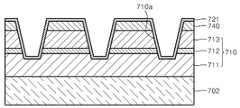
이어서, 제2 반도체층(713) 상에 제2전극층(740)을 형성한다.Subsequently, a
도 7b를 참조하면, 제2전극층(740)으로부터 소정깊이로 ICP-RIE 방법을 이용하여 제1 반도체층(711)의 일부 깊이까지 에칭한 콘택홀(710a)을 형성한다. 콘택홀(710a)을 포함하는 반도체 구조물(710)의 상부면 전역에 절연층(721)을 증착방법을 이용하여 도포한다. 예를 들어, 절연층(721)은 플라즈마 화학증착(Plasma Enhanced Chemical Vapor Deposition, PECVD)을 이용하여 SiO2또는 SiNx 를 증착하여 형성할 수 있다. 상세한 제조방법은 앞서 설명한 부분과 동일할 수 있다.Referring to FIG. 7B, a
도 7c를 참조하면, 절연층(721) 중에서 콘택홀(710a)의 바닥에 형성된 부분을 식각하여 제1 반도체층(711)을 노출시킨다. 이러한 식각은 예를 들어, RIE(Reactive Ion Etching) 건식 식각 또는 BOE(Buffered Oxide Echant)를 이용한 습식 식각방법으로 이루어질 수 있다.Referring to FIG. 7C, a portion of the insulating
절연층(721) 상으로 제1 반도체층(711)의 노출된 영역을 덮는 제1전극층(730)을 형성한다.A
제1전극층(730) 상에 다른 기판을 형성하고, 기판(702)을 제거하는 단계; 상기 다른 기판에 제1전극층 및 제2전극층과 연결되는 제1콘택과 제2콘택을 형성하는 단계는 비도전성 기판을 사용하는 제조공정(도 3g 내지 도 3j), 또는 도전성 기판을 사용하는 제조공정(도 4a-도 4c)을 참조하면 잘 알 수 있으므로 상세한 설명은 생략한다. Forming another substrate on the
또한, 제1전극층(730) 상으로 전극패드를 형성한 후 다른 기판을 형성하는 공정은 도 6a-도 6g를 참조하면 잘 알 수 있으므로, 상세한 설명은 생략한다.In addition, a process of forming another substrate after forming an electrode pad on the
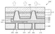
도 8은 본 발명의 다른 실시예에 따른 반도체 발광소자(800)의 개략적인 단면도이다.8 is a schematic cross-sectional view of a semiconductor
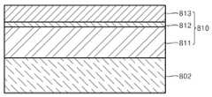
도 8을 참조하면, 본 실시예의 반도체 발광소자는 반도체 구조물(810)과, 반도체 구조물(810)의 일면(810b)에 마련된 전극 구조물을 포함한다.Referring to FIG. 8, the semiconductor light emitting device of the present embodiment includes a
반도체 구조물(810)은 소정의 기판(도 9a의 802 참조)상에 결정성장하여 형성된 제1 반도체층(811), 활성층(812), 제2 반도체층(813)을 포함한다. 결정성장의 기초가 된 기판(802)은 후술하는 바와 같이 제거될 수 있다.The
제1 반도체층(811)과 제2 반도체층(813)을 통해 주입된 전자, 정공은 활성층(812)에서 만나 빛(L)을 방출한다. 방출된 빛(L)은 반도체 구조물(810)의 타면(810c)을 통해 방출된다.Electrons and holes injected through the
전극 구조물은 제2 반도체층(813) 쪽에 마련된 제1전극층(830) 및 제2전극층(840)과, 제1전극층(830) 및 제2전극층(840)에 전기적으로 연결되는 도금 전극층(870)을 포함한다.The electrode structure may include a
제1전극층(830)은 제2 반도체층(813) 쪽에서 제1 반도체층(811)까지 연장된 콘택홀(810a)을 통해 제1 반도체층(811)에 전기적으로 연결된다. 콘택홀(810a)은 메사구조나 수직한 구조 등으로 식각되어 형성될 수 있다. 예를 들면, 콘택홀(810a)의 측면은 제1반도체층(811), 활성층(812) 및 제2반도체층(813)의 적층방향에 대해서 경사지게 형성된다. 콘택홀(810a)은 복수개 마련될 수 있다. 예를 들어, 도 10a에 도시된 바와 같이 복수의 제1전극층(830)이 형성되어, 전류 확산(current spreading)을 효과적으로 구현할 수 있다.The
제2전극층(840)은 제2 반도체층(813) 상에 마련되어 제2 반도체층(813)에 전기적으로 연결된다. 제2전극층(840)은 제2 반도체층(813)의 콘택홀(810a)이 형성되지 않은 영역(예를 들어, 도 10b의 840)에 마련될 수 있다.The
절연층(820)은 적어도 콘택홀(810a)의 측벽에 형성된다. 절연층(820)은 반도체 구조물(810)의 상면에서 제1전극층(830)이 위치한 영역 및 제2전극층(840)이 위치한 영역의 일부를 제외한 나머지 영역에 도포되어 있다. 제1전극층(830)은 절연층(820)에 의해, 활성층(812), 제2 반도체층(813) 및 제2전극층(840)으로부터 절연된다.The insulating
절연층(820) 상에는 도금 전극층(870)이 마련된다. 도금 전극층(870)은 절연 격벽(880)을 사이에 둔 제1 전극패드(871)와 제2 전극패드(872)를 포함한다. 제1 전극패드(871)는 제1전극층(830)이 위치한 제1 전극 영역에 마련되며, 제2 전극패드(872)는 제2전극층(840)이 위치한 제2 전극 영역에 마련된다. 제1 전극패드(871)와 제2 전극패드(872)는 절연 격벽(880)에 의해 분리될 수 있다. 절연 격벽(880)은 통상의 절연물질, 예를 들어 폴리이미드 등의 물질로 형성될 수 있다.The
도금 전극층(870)은 예를 들어 구리, 니켈, 크롬 등의 금속으로 수십 μm의 두께로 도금에 의해 형성될 수 있다. 도금을 용이하게 하기 위하여, 제1 전극패드(871)와 제2 전극패드(872)의 하부에는 시드층(850)이 먼저 마련될 수 있다.The
본 실시예의 반도체 발광소자(800)는, 상기와 같이 도금공정으로 형성되는 도금 전극층(870)으로 반도체 구조물(810)에 대한 전기적 배선과 물리적 지지가 이루어지도록 함으로써, 대량생산, 대면적화가 용이하면서, 제조비용을 저감시킬 수 있다. 이러한 점은 통상의 반도체 발광소자가, 반도체 구조물(810)과 전극 기판의 기판접합을 통하여, 반도체 구조물(810)에 대한 전기적 배선과 물리적 지지를 이루는 것과 차이가 있다.In the semiconductor
다음으로, 일 실시예에 따른 반도체 발광소자의 제조방법을 설명하기로 한다.Next, a method of manufacturing a semiconductor light emitting device according to an embodiment will be described.
도 9a 내지 도 9l은 본 발명의 다른 실시예에 따른 반도체 발광소자의 제조방법을 설명하기 위해 순차적으로 도시한 공정단면도이며, 도 10a 내지 도 10d는 본 발명의 다른 실시예에 따른 반도체 발광소자의 제조 공정의 단계에서 전극 패턴의 일예를 도시한 평면도이다.9A to 9L are cross-sectional views sequentially illustrating a method of manufacturing a semiconductor light emitting device according to another embodiment of the present invention, and FIGS. 10A to 10D are views of a semiconductor light emitting device according to another embodiment of the present invention. It is a top view which shows an example of an electrode pattern in the step of a manufacturing process.
도 9a를 참조하면, 기판(802)의 상면에 제1 반도체층(811), 활성층(812) 및 제2 반도체층(813)을 순차적으로 결정성장시켜 반도체 구조물(810)을 형성한다. 도 9a에는 도시되지 않았지만, 기판(802)과 제1 반도체층(811)의 사이에는 버퍼층(미도시)이 형성될 수 있다.Referring to FIG. 9A, a
도 9b를 참조하면, 제2 반도체층(813)으로부터 소정 깊이로 에칭하여 콘택홀(810a)을 형성하여 제1 반도체층(811)의 일부를 노출시킨다. 콘택홀(810a)은 앞서 설명한 구조 등으로 형성할 수 있다. 이때, 콘택홀(810a)은 도 10a에 도시된 복수의 제1전극층(830)에 대응되도록 복수개 형성될 수 있다.Referring to FIG. 9B, a
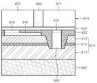
다음으로, 콘택홀(810a)을 포함하는 반도체 구조물(810)의 상부면 전역에 보호층(Passivation layer, 821)을 증착방법을 이용하여 도포한다. 예를 들어, 보호층(821)은 플라즈마 화학증착(Plasma Enhanced Chemical Vapor Deposition, PECVD)을 이용하여 SiO2를 약 6000ÅÅ두께로 증착하여 형성할 수 있다.Next, a
도 9c를 참조하면, 보호층(821) 중에서 콘택홀(810a)의 바닥에 형성된 부분을 식각하여 제1 반도체층(811)을 노출시킨다. 이러한 식각은 예를 들어, RIE(Reactive Ion Etching)와 BOE(Buffered Oxide Echant)를 이용하여 이루어질 수 있다. 다음으로, 제1 반도체층(811)의 노출된 영역에 제1전극층(830)을 형성한다.Referring to FIG. 9C, a portion of the
제1전극층(830)은 Al, Ti, Pt, Ag, Ni, TiN, Au, Sn, 및 이들 혼합물 중의 적어도 하나를 포함하여 형성될 수 있으며, 단층 혹은 서로 다른 물질의 복수의 층으로 구성 될 수 있다. 각 층의 두께는 각각 0.1 ~ 5000nm로 형성될 수 있다. 예를 들어, 본 실시예에서는 제1전극층(830)은 Al/Ti/Pt/Ti층을 200nm/300nm/100nm/2nm의 두께로 증착하여 형성할 수 있다. 이때, 제1전극층(830)은 도 10a에 도시되듯이 다수개 형성하여, 제1 반도체층(811)으로의 전류 확산(current spreading)을 향상시킬 수 있다. 제1전극층(830)은 매트릭스 형태로 배열되어 형성될 수 있으며, 이는 최적의 전류 확산을 위한 것이다. 제1전극층(830) 형성후에는 오믹콘택 형성을 위한 열처리를 행한다. 본 실시예에서 열처리는 RTA(rapid thermal annealing)법으로 550℃에서 60초간 실시 하여 양호한 오믹 특성을 얻었다. 열처리의 온도 및 시간은 오믹 전극의 재료에 따라 다르지만 300 ~ 800℃에서 5 ~ 5000초 정도에서 행해 질 수 있다. 적절하게는 300 ~ 600℃에서 30 ~ 180초가 좋다.The
콘택홀(180)은 전류 확산 및 광 추출을 고려하여 매트릭스로 배열될 수 있다.The contact holes 180 may be arranged in a matrix in consideration of current spreading and light extraction.
도 9d를 참조하면, 제1전극층(830)을 둘러싼 영역을 제외한 나머지 영역의 보호층(821)을 식각하여, 제2 반도체층(813)을 노출시킨다. 이러한 식각은 예를 들어, RIE와 BOE를 이용하여 이루어질 수 있다. 다음으로, 노출된 제2 반도체층(813) 상에 제2전극층(840)을 형성한다. 이때, 제2전극층(840)은 도 10b에 도시되듯이, 제1전극층(830)에서 이격되도록 형성된다. 제2전극층(840)은 오믹특성과 광반사특성을 동시에 지닌 금속으로 형성되어 반사막의 역할을 하거나, 또는 오믹특성과 광반사특성을 각각 지닌 금속이 순차 적층되어 이루어진 다층으로 형성할 수 있다. 예를 들어, 제2전극층(840)은 Ag/Ni/Ti/TiN층을 150nm/ 50nm/50nm/400nm의 두께로 증착하여 형성할 수 있다. 제2전극층(840) 형성후 오믹콘택 형성을 위한 열처리를 행한다. 본 실시예에서는 열처리로 RTA법을 사용하여 350℃에서 60초간 실시하여 양호한 오믹 특성을 얻었다. 열처리의 온도 및 시간은 오믹 전극의 재료에 따라 다르지만 300 ~ 800℃에서 5 ~ 5000초 정도에서 행해 질 수 있다. 적절하게는 300 ~ 600℃에서 30 ~ 180초가 좋다.Referring to FIG. 9D, the
도 9e에 도시되듯이, 반도체 구조물(810)의 상측에 소정 두께로 절연물질층(822)을 도포한다. 절연물질층(822)은 제1전극층(830), 제2전극층(840) 및 보호층(821)을 포괄한 전역에 도포된다. 이러한 절연물질층(822)은 예를 들어, PECVD를 이용하여 SiO2를 약 8000ÅÅ두께로 증착하여 형성할 수 있다. 보호층(821) 및 절연물질층(822)은 동일 물질로 형성될 수 있으며, 제1전극층(830) 및 제2전극층(840)에 대한 절연층(820)을 이룬다. 절연물질층(822)의 두께는 제1전극층의 상면을 덮을 정도의 두께로 하며, 적절하게는 100nm ~ 10000nm로 할 수 있다. 절연층(820) 두께는 200nm ~ 20000nm로 형성 할 수 있다.도 9f를 참조하면, 절연층(820)을 식각하여 제1전극층(830)과 제2전극층(840)을 노출시킨다. 이때, 제1전극층(830)이 복수개 형성된 경우, 도 10c에 도시된 바와 같이 모든 제1전극층(830)들을 노출시킨다. 한편, 제2전극층(840)은 소정 영역만을 노출시킬 수 있다. 노출된 제1전극층(830)과 제2전극층(840) 각각에는 구리, 니켈, 크롬과 같은 금속물질(835, 845)을 채울 수 있다. 제1전극층(830)이 복수로 형성된 경우, 금속물질(835)는 복수의 제1전극층(830)을 연결하도록 형성될 수 있다. 이러한 공정은 전술한 공정, 예컨대 도 3f에 도시된 공정에서 잘 알 수 있으므로 상세한 설명은 생략한다.As shown in FIG. 9E, an insulating
도 9g에 도시되듯이, 제1전극층(830)과 제2전극층(840) 상에 도금을 위한 시드층(850)을 형성한다.As shown in FIG. 9G, the
다음으로, 도 9h에 도시되듯이, 시드층(850) 상으로 포토레지스트(860)를 형성한다. 포토레지스트(860)은 절연층(820) 상방으로 형성된다.Next, as shown in FIG. 9H, a
도 9i에 도시되듯이, 시드층(850) 상으로 도금공정으로 도금전극층(870)을 형성한다. 도금전극층(870)은 포토레지스트(860)를 사이에 두고, 제1 전극패드(871)와 제2 전극패드(872)로 형성된다. 제1 전극패드(871)와 제2 전극패드(872)는 구리, 니켈, 크롬 등의 금속으로 5 ~ 500μm의 두께로 형성할 수 있다. 도 10d와 같이, 제1전극패드(871)와 제2전극패드(872)는 포토레지스트(860)를 사이에 두고 형성된다.As shown in FIG. 9I, the
9j에 도시되듯이, 포토레지스트(860)를 제거하여 제1 전극패드(871)와 제2 전극패드(872) 사이의 공간(gap)(870a)을 확보한다.As shown in FIG. 9J, the
도 9k에 도시되듯이 시드층(850)을 식각하여 시드층(850)을 제1시드층(851)과 제2시드층(852)으로 분리한다. 제1시드층(851)은 포토레지스트(860)가 있던 공간(870a)에 절연물질을 채워 절연 격벽(880)을 형성한다. 절연 격벽(880)을 형성한 후 CMP(Chemical Mechanical Polishing)와 같은 공정을 통해 도금 전극층(870)의 표면을 평탄화시킬 수 있다.As shown in FIG. 9K, the
도 9l에 도시되듯이, 결정성장의 기초가 된 기판(802)을 레이저 리프트 오프(laser lift off) 공정등을 통해 제거한다. 제1시드층(851)의 면적은 제1전극층(830)의 면적 보다 크게 하는 것이 바람직하며, 제2시드층(852)의 면적은 제2 전극층(840)의 면적 보다 크게 하는 것이 바람직하다.As shown in FIG. 9L, the
본 실시예의 반도체 발광소자는 전술한 바와 같이 도금 공정을 통해 도금 전극층(870)을 형성하기에, 별도로 전극 기판을 준비할 필요도 없고, 반도체 구조물(810)을 전극 기판과 기판접합할 필요도 없다. 따라서, 본 실시예의 반도체 발광소자의 제조방법은 공정 비용이 저렴하며, 대량생산 및 대면적화가 용이하다. 또한, 도금 전극층(870)을 반도체 구조물(810)의 한쪽면에 형성하므로, 플립칩 공정을 통해 칩 레벨에서 패키징이 가능하다. 나아가, 도금 전극층(870)을 모두 열전도도가 좋은 금속으로 형성하므로, 방열효과가 크며, 장시간 동작이 가능한 고신뢰성의 고출력 발광소자칩 구현이 가능하다.Since the semiconductor light emitting device of the present embodiment forms the
또한, 종래의 반도체 발광소자에서 전극구조물을 한쪽면에 모두 형성하고자 하는 경우, 반도체 구조물(810)에 별도의 전극 기판을 부착하는데, 웨이퍼의 휨(bowing) 현상등에 의해 전극 기판 부착시 정렬불일치(misalignment)가 발생될 위험이 있는데, 본 실시예의 반도체 발광소자는, 별도의 전극 기판의 부착이 불필요하므로, 정렬불일치의 문제등이 발생될 여지가 없다.In addition, when the electrode structure is to be formed on one side of the conventional semiconductor light emitting device, a separate electrode substrate is attached to the
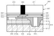
도 11은 본 발명의 다른 실시예에 따른 반도체 발광소자(900)의 개략적인 단면도이다.11 is a schematic cross-sectional view of a semiconductor
도 11을 참조하면, 본 실시예의 반도체 발광소자(900)는 반도체 구조물(810)과, 반도체 구조물(810)의 일면(810b)에 마련된 전극 구조물을 포함한다.Referring to FIG. 11, the semiconductor
반도체 구조물(810)은 소정의 기판(도 12a의 802 참조) 상에 결정성장하여 형성된 제1 반도체층(811), 활성층(812), 제2 반도체층(813)을 포함한다. 결정성장의 기초가 된 기판(802)은 후술하는 바와 같이 제거될 수 있다.The
전극 구조물은 제2 반도체층(813) 쪽에 마련된 제1전극층(830) 및 제2전극층(840)과, 제1전극층(830) 및 제2전극층(840)에 전기적으로 연결되는 도금 전극층(970)을 포함한다.The electrode structure may include a
제1전극층(830)은 제2 반도체층(813) 쪽에서 제1 반도체층(811)으로 뚫린 콘택홀(810a)을 통해 제1 반도체층(811)에 전기적으로 연결된다. 콘택홀(810a)은 메사구조나 수직한 구조 등으로 식각되어 형성될 수 있다. 콘택홀(810a)은 복수개 마련될 수 있다. 복수의 제1전극층(830)이 형성되어, 전류 확산(current spreading)을 효과적으로 구현할 수 있다.The
제2전극층(840)은 제2 반도체층(813) 상에 마련되어 제2 반도체층(813)에 전기적으로 연결된다. 제2전극층(840)은 제2 반도체층(813)의 콘택홀(810a)이 형성되지 않은 영역에 마련될 수 있다.The
절연층(820)은 반도체 구조물(810)의 상면에서 제1전극층(830)이 위치한 영역 및 제2전극층(840)이 위치한 영역의 일부를 제외한 나머지 영역에 도포되어 있다. 제1전극층(830)은 절연층(820)에 의해, 활성층(812), 제2 반도체층(813) 및 제2전극층(840)으로부터 절연된다.The insulating
절연층(820) 상에는 제1전극층(830) 및 제2전극층(840)과 각각 연결되는 제1 금속층(951) 및 제2 금속층(952)이 형성된다. 제1 금속층(951)은 복수의 제1전극층(930)과 연결되게 형성되므로 면적이 넓으며, 제2 금속층(952)은 일부 영역에만 형성된다. 발광소자(900)의 크기에 따라 달라 질 수 있으나 제1 금속층(951)의 면적은 제2 금속층(952)의 면적보다 3배 이상인 것이 바람직하다.제1 금속층(951) 및 제2 금속층(952)과 연결되게 제3 금속층(953) 및 제4 금속층(954)이 형성되어 있다. 제3 금속층(953)은 제1 금속층(951)의 영역 보다 좁게 형성되며, 제4 금속층(954)은 제 2 금속층(952)의 영역과 비슷한 영역을 차지한다.The
절연층(956)은 제1 금속층(951) 및 제2 금속층(952) 사이의 공간과, 제3 금속층(953) 및 제4 금속층(954) 사이의 공간을 채워서, 제1 금속층(951) 및 제2 금속층(952)을 절연시키며, 제3 금속층(953) 및 제4 금속층(954)을 절연시킨다.The insulating
절연층(956) 상에는 절연격벽(980)이 형성되어 있다. 절연격벽(980)의 양측에는 각각 제3 금속층(953) 및 제4 금속층(954)와 연결된 제1 시드층(961)과 제2 시드층(962)이 형성되어 있다. 제1 시드층(961) 및 제2 시드층(962) 상에는 각각 제1 전극패드(971)과 제2 전극패드(972)가 형성된다. 제1 전극패드(971) 및 제2 전극패드(972)는 도금공정으로 형성될 수 있다. 제1전극패드(971) 및 제2전극패드(972)의 도금두께는 15 ~ 500μm가 적당하며 전극 재료로는 Al, Ti, Pt, Ag, Ni, TiN, Au, Sn, 및 이들 혼합물 중의 적어도 하나를 포함하여 형성될 수 있다. 두께가 15μm보다 얇으면 지지기판으로의 역할을 제대로 할 수 없으며 500μm보다 두꺼우면 도금공정 시간이 길어지고 비용이 증가하는 문제가 있다. 절연격벽(980)의 폭(제1 전극패드(971) 와 제2 전극패드(972) 간격)은 1μm ~ 500μm정도가 적당하다. 절연 격벽(980)의 폭이 1μm이하이면 양쪽 전극(971, 972) 사이의 절연 공정이 어려울 수 있으며, 500μm이상이면 전극패드(971, 972)의 크기가 상대적으로 작아져 발광소자(900)에서 발생하는 열의 방열을 효과적으로 제거하지 못해 발광소자(900)의 온도가 상승하여 발광소자(900)의 휘도 저하 등의 성능이 불량해질 수 있다.An insulating
본 실시예의 반도체 발광소자(900)는, 제1전극층(830) 및 제2전극층(840)과 제1 시드층(961) 및 제2 시드층(962) 사이에 금속층 및 절연층을 형성함으로써 제2 전극패드(972)의 면적을 넓게 형성할 수 있으며, 이에 따라 반도체 발광소자(900)는 콘택이 형성된 기판과의 접속을 위해서 용이하게 전극패드(971, 972)의 위치 및 면적을 변경할 수 있다.The semiconductor
다음으로, 다른 실시예에 따른 반도체 발광소자의 제조방법을 설명한다.Next, a method of manufacturing a semiconductor light emitting device according to another embodiment will be described.
도 12a 내지 도 12g는 본 발명의 또 다른 실시예에 따른 반도체 발광소자의 제조방법을 설명하기 위해 순차적으로 도시한 공정단면도이며, 도 13a 내지 도 13c는 본 발명의 일 실시예에 따른 반도체 발광소자의 제조 공정의 단계에서 전극 패턴의 일예를 도시한 평면도이다.12A to 12G are cross-sectional views sequentially illustrating a method of manufacturing a semiconductor light emitting device according to still another embodiment of the present invention, and FIGS. 13A to 13C are semiconductor light emitting devices according to an embodiment of the present invention. It is a top view which shows an example of the electrode pattern in the step of the manufacturing process of the.
도 12a는 도 9a 내지 도 9f의 공정의 후속공정이며, 도 9a 내지 도 9f의 공정에 대해서는 상세한 설명은 생략한다.12A is a subsequent step of the process of FIGS. 9A to 9F, and detailed description of the process of FIGS. 9A to 9F will be omitted.
도 12a를 참조하면, 제1전극층(830)과 제2전극층(840) 상에 금속층(미도시)을 형성한 다음, 금속층을 패터닝하여 제1전극층(830) 및 제2전극층(840)과 각각 연결된 제1 금속층(951) 및 제2 금속층(952)을 형성한다. 도 13a를 참조하면, 제1 금속층(951)은 복수의 제1전극층(830)과 연결되므로 면적이 넓으며, 제2 금속층(952)은 일부 영역에만 형성된다. 제1금속층(951)과 제2금속층(952)의 형성은 선공정인 도 9f의 공정에서 각각 금속물질(835, 845)와 함께 수행될 수도 있다.Referring to FIG. 12A, a metal layer (not shown) is formed on the
도 12b를 참조하면, 절연층(820) 상으로 제1 금속층(951) 및 제2 금속층(952)을 덮는 절연층(956)을 형성한다. 이어서, 절연층(956)을 패터닝하여 제1 금속층(951) 및 제2 금속층(952)을 각각 노출시킨 다음, 노출된 영역에 각각 제1 금속층(951) 및 제2 금속층(952)과 연결되게 제3 금속층(953) 및 제4 금속층(954)을 형성한다. 도 13a 및 도 13b를 함께 참조하면, 제3 금속층(953)은 제1 금속층(951)의 영역 보다 좁게 형성되며, 제4 금속층(954)은 제 2 금속층(952)의 영역의 0.5 ~ 3배 면적을 차지하도록 형성한다..12B, an insulating
도 12c를 참조하면, 절연층(956) 상으로 제3 금속층(953) 및 제4 금속층(954)을 덮는 도금을 위한 시드층(960)을 형성한다. 이어서, 시드층(960) 상에 시드층(960)을 둘로 나누는 포토레지스트(964)를 형성한다. 도 13c를 참조하면, 포토레지스트(964)로 나뉘는 제1영역(A1)과 제2영역(A2)은 각각 제3 금속층(953) 및 제4 금속층(954)와 접촉하는 영역이다. 제2영역(A2)는 제4 금속층(954)의 1-5 배 면적으로 형성된다.Referring to FIG. 12C, a
도 12d를 참조하면, 포토레지스트(964)를 사이에 두고, 제1영역(A1)과 제2영역(A2) 각각에 제1 전극패드(971)와 제2 전극패드(972)를 도금 공정으로 형성한다. 제1 전극패드(971)와 제2 전극패드(972)는 구리, 니켈, 크롬 등의 금속으로 15 ~ 500μm의 두께로 형성할 수 있다.Referring to FIG. 12D, the
도 12e를 참조하면, 포토레지스트(964)를 제거하여 제1 전극패드(971)와 제2 전극패드(972) 사이의 공간(gap)(970a)를 확보한다. 공간(970a)의 폭(제1 전극패드(971)와 제2 전극패드(972)의 간격)은 1μm ~ 500μm정도가 적당하다. 공간(970a)의 폭이 1μm이하이면 양쪽 전극패드(971, 972) 사이의 절연 공정의 불량이 발생될 수 있다. 500μm이상이면 전극패드(971, 972)가 차지하는 면적이 상대적으로 작아져 발광소자에서 발생하는 열의 방출을 효과적으로 하지 못해 발광소자의 온도가 상승하여 발광소자의 휘도 저하 등의 성능이 불량해질 수 있다.Referring to FIG. 12E, the
도 12f를 참조하면, 포토레지스트(964)가 있던 공간(970a)에 노출된 시드층(960)을 식각하여 제1 시드층(961)과 제2 시드층(962)로 분리한다. 이어서, 공간(970a)과, 제1 시드층(961) 및 제2 시드층(962)의 식각된 영역을 채워서 절연 격벽(980)을 형성한다. 절연 격벽(980)을 형성한 후 CMP(Chemical Mechanical Polishing)와 같은 공정을 통해 제1 전극패드(971)와 제2 전극패드(972)의 표면을 평탄화시킬 수 있다.Referring to FIG. 12F, the
도 12g를 참조하면, 결정성장의 기초가 된 기판(802)을 레이저 리프트 오프(laser lift off) 공정 등을 통해 제거한다.Referring to FIG. 12G, the
상기 실시예에 따르면, 상술한 바와 같이 도금공정으로 전극패드를 형성할 수 있으며, 전극패드의 형성영역을 용이하게 설계할 수 있어서, 제조된 발광소자를 다른 콘택이 형성된 기판에 용이하게 설치할 수 있다.According to the above embodiment, the electrode pad can be formed by the plating process as described above, and the formation region of the electrode pad can be easily designed, so that the manufactured light emitting device can be easily installed on a substrate on which other contacts are formed. .
이상에서 본 발명의 실시예가 설명되었으나, 이는 예시적인 것에 불과하며, 당해 분야에서 통상적 지식을 가진 자라면 이로부터 다양한 변형 및 균등한 타 실시예가 가능하다는 점을 이해할 것이다. 이상에서 첨부된 도면을 참조하여 설명된 본 발명의 실시예들은 예시적인 것에 불과하며, 당해 분야에서 통상의 지식을 가진 자라면 이로부터 다양한 변형 및 균등한 타 실시예가 가능함을 이해할 수 있을 것이다. 따라서 본 발명의 진정한 보호범위는 첨부된 특허청구범위에 의해서만 정해져야 할 것이다.While the invention has been shown and described with reference to certain preferred embodiments thereof, it will be understood by those skilled in the art that various changes and modifications may be made without departing from the scope of the invention as defined by the appended claims. While the invention has been shown and described with reference to certain embodiments thereof, it will be understood by those skilled in the art that various changes and modifications may be made without departing from the scope of the invention as defined by the appended claims. Therefore, the true scope of protection of the present invention should be defined only by the appended claims.
Claims (71)
Translated fromKorean상기 기판을 관통하여 상기 제1전극층과 전기적으로 연결된 제1콘택과, 상기 기판, 상기 제1전극층 및 상기 절연층을 관통하여 상기 제2전극층과 통전하는 제2콘택;을 구비하며,
상기 제1전극층은 상기 제2전극층, 제2반도체층 및 활성층을 관통하는 콘택홀을 채워서 상기 제1반도체층과 전기적으로 연결되며,
상기 절연층은 상기 콘택홀의 내주를 감싸도록 형성되어 상기 제1전극층을 상기 제2전극층으로부터 절연하는 반도체 발광소자.A first electrode layer, an insulating layer, a second electrode layer, a second semiconductor layer, an active layer, and a first semiconductor layer sequentially stacked on a substrate;
A first contact penetrating the substrate and electrically connected to the first electrode layer, and a second contact penetrating the substrate, the first electrode layer, and the insulating layer to conduct electricity with the second electrode layer;
The first electrode layer is electrically connected to the first semiconductor layer by filling contact holes penetrating through the second electrode layer, the second semiconductor layer, and the active layer.
The insulating layer is formed to surround the inner circumference of the contact hole to insulate the first electrode layer from the second electrode layer.
상기 콘택홀은 복수이며, 각 콘택홀은 상기 제1전극층으로 채워진 반도체 발광소자.The method of claim 1,
The plurality of contact holes, each contact hole is filled with the first electrode layer.
상기 제2콘택의 외주에 적어도 상기 제2콘택과 상기 제1전극층을 절연하는 절연층이 더 구비한 반도체 발광소자.The method of claim 1,
And an insulating layer insulated from at least the second contact and the first electrode layer on an outer circumference of the second contact.
상기 제2전극층은 상기 활성층으로부터 발생한 광을 반사시키는 반사층인 반도체 발광 소자.The method of claim 1,
The second electrode layer is a semiconductor light emitting device that reflects the light generated from the active layer.
상기 제2전극층은 Ag, Al, Pt, Ni, Pd, Ti, Au, Ir, W, Sn, 이들의 산화물 또는 이들의 혼합물로 구성된 그룹으로부터 선택된 적어도 어느 하나의 물질로 형성된 반도체 발광 소자.The method of claim 4, wherein
The second electrode layer is formed of at least one material selected from the group consisting of Ag, Al, Pt, Ni, Pd, Ti, Au, Ir, W, Sn, oxides thereof or mixtures thereof.
상기 기판은 알루미나, 알루미늄 나이트라이드, 사파이어, 폴리머 중 어느 하나의 물질로 형성된 비도전성 기판인 반도체 발광 소자.The method of claim 1,
The substrate is a semiconductor light emitting device that is a non-conductive substrate formed of any one material of alumina, aluminum nitride, sapphire, polymer.
상기 기판은 도전성 기판이며, 상기 제1콘택 및 상기 제2콘택이 형성된 관통홀의 내주와 상기 도전성 기판의 표면에 절연층이 형성된 반도체 발광 소자.The method of claim 1,
The substrate is a conductive substrate, the semiconductor light emitting device having an insulating layer formed on the inner circumference of the through-hole formed with the first contact and the second contact and the surface of the conductive substrate.
상기 기판은 Si, Ge, 및 Al을 포함하는 Si 중 선택된 어느 하나를 포함하는 반도체 발광 소자.The method of claim 7, wherein
The substrate includes any one selected from Si, Ge, and Si including Al.
상기 제2반도체층으로부터 상기 제1반도체층을 노출하는 콘택홀을 형성하고, 상기 콘택홀에 상기 제1반도체층과 연결되게 콘택층을 형성하는 단계;
상기 제2반도체층 상으로 상기 콘택홀의 외부에 형성되어 상기 콘택홀을 둘러싸는 제2전극층을 형성하는 단계;
상기 제2전극층 상으로 제1절연층을 형성하는 단계;
상기 제1절연층 상으로 상기 콘택층과 연결된 제1전극층을 형성하는 단계;
제2기판을 상기 제1전극층 상에 접합하고, 상기 제1기판을 제거하는 단계;
상기 제2기판의 노출면으로부터 상기 제1전극층과 연결되는 제1관통홀과, 상기 제2전극층과 연결되는 제2관통홀을 형성하는 단계; 및
상기 제1관통홀과 상기 제2관통홀을 각각 메탈로 채워서 상기 제1전극층과 상기 제2전극층에 각각 연결되는 제1콘택 및 제2콘택을 형성하는 단계;를 포함하는 반도체 발광소자의 제조방법.Sequentially forming a first semiconductor layer, an active layer, and a second semiconductor layer on the first substrate;
Forming a contact hole exposing the first semiconductor layer from the second semiconductor layer, and forming a contact layer in the contact hole so as to be connected to the first semiconductor layer;
Forming a second electrode layer formed outside the contact hole on the second semiconductor layer to surround the contact hole;
Forming a first insulating layer on the second electrode layer;
Forming a first electrode layer connected to the contact layer on the first insulating layer;
Bonding a second substrate on the first electrode layer, and removing the first substrate;
Forming a first through hole connected to the first electrode layer and a second through hole connected to the second electrode layer from an exposed surface of the second substrate; And
Forming a first contact and a second contact respectively connected to the first electrode layer and the second electrode layer by filling the first through hole and the second through hole with metal, respectively; .
상기 콘택홀을 덮는 제2절연층을 형성하는 단계;
상기 콘택홀의 바닥의 상기 제2절연층을 식각하여 상기 제1반도체층을 노출시키는 단계;를 더 포함하며,
상기 콘택층 형성단계는 상기 노출된 제1반도체층 상으로 상기 콘택층을 형성하는 단계인 반도체 발광소자의 제조방법.The method of claim 16, wherein the forming of the contact hole comprises:
Forming a second insulating layer covering the contact hole;
And etching the second insulating layer on the bottom of the contact hole to expose the first semiconductor layer.
The forming of the contact layer is a step of forming the contact layer on the exposed first semiconductor layer.
상기 콘택홀 및 상기 콘택층 형성단계는, 복수의 콘택홀과 복수의 콘택층을 형성하는 단계인 반도체 발광소자의 제조방법.17. The method of claim 16,
The forming of the contact hole and the contact layer is a step of forming a plurality of contact holes and a plurality of contact layers.
상기 제2전극층 형성 단계는,
상기 제2반도체층 상으로 제3절연층을 형성하는 단계;
상기 콘택홀의 외부에 형성되어 상기 콘택홀을 둘러싸는 제3절연층을 제거하여 상기 제2반도체층을 노출하는 단계; 및
상기 노출된 제2반도체층 상으로 상기 제2전극층을 형성하는 단계;를 포함하는 반도체 발광소자의 제조방법.The method of claim 18,
The second electrode layer forming step,
Forming a third insulating layer on the second semiconductor layer;
Exposing the second semiconductor layer by removing a third insulating layer formed outside the contact hole and surrounding the contact hole; And
And forming the second electrode layer on the exposed second semiconductor layer.
상기 제2전극층은 Ag, Al, Pt, Ni, Pd, Ti, Au, Ir, W, Sn, 이들의 산화물 또는 이들의 혼합물로 구성된 그룹으로부터 선택된 적어도 어느 하나의 물질로 형성하는 반도체 발광소자의 제조방법.17. The method of claim 16,
The second electrode layer is formed of at least one material selected from the group consisting of Ag, Al, Pt, Ni, Pd, Ti, Au, Ir, W, Sn, oxides thereof or mixtures thereof. Way.
상기 콘택층을 노출하도록 상기 제1절연층을 식각하는 단계; 및
상기 노출된 콘택층을 덮도록 상기 제1전극층을 형성하는 단계;를 포함하는 반도체 발광소자의 제조방법.The method of claim 16, wherein the first electrode layer forming step,
Etching the first insulating layer to expose the contact layer; And
And forming the first electrode layer to cover the exposed contact layer.
상기 제2관통홀의 내주에 제4절연층을 형성하는 단계를 더 포함하는 반도체 발광소자의 제조방법.The method of claim 16, wherein the forming of the second through hole comprises:
And forming a fourth insulating layer on the inner circumference of the second through hole.
상기 제2기판은 알루미나, 알루미늄 나이트라이드, 사파이어, 폴리머 중 선택된 어느 하나의 물질로 형성된 비도전성 기판인 반도체 발광소자의 제조방법.17. The method of claim 16,
And the second substrate is a non-conductive substrate formed of any one material selected from alumina, aluminum nitride, sapphire, and polymer.
상기 제2반도체층으로부터 상기 제1반도체층을 노출하는 콘택홀을 형성하고, 상기 콘택홀에 상기 제1반도체층과 연결되게 콘택층을 형성하는 단계;
상기 제2반도체층 상으로 상기 콘택홀의 외부에 형성되어 상기 콘택홀을 둘러싸는 제2전극층을 형성하는 단계;
상기 제2전극층 상으로 제1절연층을 형성하는 단계;
상기 제1절연층 상으로 상기 콘택층과 연결된 제1전극층을 형성하는 단계;
제2기판에 상기 제1전극층과 연결되는 제1관통홀과, 상기 제2전극층과 연결되는 제2관통홀을 형성하는 단계;
상기 제1관통홀과 상기 제2관통홀을 각각 메탈로 채워서 상기 제1전극층과 상기 제2전극층에 각각 연결되는 제1콘택 및 제2콘택을 형성하는 단계;
상기 제1전극층의 노출된 표면에서 상기 제1전극층으로부터 절연되며, 상기 제2전극층에 연결되는 제3콘택을 형성하는 단계;
상기 제3콘택과 상기 제2콘택이 접촉하도록 상기 제2기판을 상기 제1전극층 상에 접합하는 단계; 및
상기 제1기판을 제거하는 단계;를 포함하는 반도체 발광소자의 제조방법.Sequentially stacking a first semiconductor layer, an active layer, and a second semiconductor layer on a first substrate;
Forming a contact hole exposing the first semiconductor layer from the second semiconductor layer, and forming a contact layer in the contact hole so as to be connected to the first semiconductor layer;
Forming a second electrode layer formed outside the contact hole on the second semiconductor layer to surround the contact hole;
Forming a first insulating layer on the second electrode layer;
Forming a first electrode layer connected to the contact layer on the first insulating layer;
Forming a first through hole connected to the first electrode layer and a second through hole connected to the second electrode layer on a second substrate;
Filling the first through hole and the second through hole with metal to form first and second contacts respectively connected to the first electrode layer and the second electrode layer;
Forming a third contact insulated from the first electrode layer on the exposed surface of the first electrode layer and connected to the second electrode layer;
Bonding the second substrate on the first electrode layer such that the third contact and the second contact come into contact with each other; And
Removing the first substrate; and manufacturing the semiconductor light emitting device.
상기 제2기판은 Si, Ge, 및 Al을 포함하는 Si, 및 GaN 중 선택된 어느 하나를 포함하는 반도체 발광 소자의 제조방법.The method of claim 25,
The second substrate is a method for manufacturing a semiconductor light emitting device comprising any one selected from Si, Ge, and Al, including Ga, and GaN.
상기 콘택홀형성단계는,
상기 콘택홀을 덮는 제3절연층을 형성하는 단계;
상기 콘택홀의 바닥의 상기 제3절연층을 식각하여 상기 제1반도체층을 노출시키는 단계;를 더 포함하며,
상기 콘택층 형성단계는 상기 노출된 제1반도체층 상으로 상기 콘택층을 형성하는 단계인 반도체 발광소자의 제조방법.25. The method of claim 24,
The contact hole forming step,
Forming a third insulating layer covering the contact hole;
And etching the third insulating layer on the bottom of the contact hole to expose the first semiconductor layer.
The forming of the contact layer is a step of forming the contact layer on the exposed first semiconductor layer.
상기 콘택홀 및 상기 콘택층 형성단계는, 복수의 콘택홀과 복수의 콘택층을 형성하는 단계인 반도체 발광소자의 제조방법.25. The method of claim 24,
The forming of the contact hole and the contact layer is a step of forming a plurality of contact holes and a plurality of contact layers.
상기 제2반도체층 상으로 제4절연층을 형성하는 단계;
상기 콘택홀의 외부에 형성되어 상기 콘택홀을 둘러싸는 상기 제4절연층을 제거하여 상기 제2반도체층을 노출하는 단계; 및
상기 노출된 제2반도체층 상으로 상기 제2전극층을 형성하는 단계;를 포함하는 반도체 발광소자의 제조방법.The method of claim 27, wherein the second electrode layer forming step,
Forming a fourth insulating layer on the second semiconductor layer;
Exposing the second semiconductor layer by removing the fourth insulating layer formed outside the contact hole and surrounding the contact hole; And
And forming the second electrode layer on the exposed second semiconductor layer.
상기 제2전극층은 Ag, Al, Pt, Ni, Pd, Ti, Au, Ir, W, Sn, 이들의 산화물 또는 이들의 혼합물로 구성된 그룹으로부터 선택된 적어도 어느 하나의 물질로 형성하는 반도체 발광소자의 제조방법.25. The method of claim 24,
The second electrode layer is formed of at least one material selected from the group consisting of Ag, Al, Pt, Ni, Pd, Ti, Au, Ir, W, Sn, oxides thereof or mixtures thereof. Way.
상기 콘택층을 노출하도록 상기 제1절연층을 식각하는 단계; 및
상기 노출된 콘택층을 덮도록 상기 제1전극층을 형성하는 단계;를 포함하는 반도체 발광소자의 제조방법.The method of claim 24, wherein the forming of the first electrode layer,
Etching the first insulating layer to expose the contact layer; And
And forming the first electrode layer to cover the exposed contact layer.
상기 제2전극층으로부터 상기 제1반도체층을 노출하는 콘택홀을 형성하는 단계;
상기 제2전극층 상으로 상기 콘택홀의 내주를 덮는 제1절연층을 형성하는 단계;
상기 콘택홀의 바닥을 식각하여 상기 제1반도체층을 노출시키는 단계;
상기 제1절연층 상으로 노출된 제1반도체층과 접촉하는 제1전극층을 형성하는 단계;
제2기판을 상기 제1전극층 상에 접합하고, 상기 제1기판을 제거하는 단계;
상기 제2 기판의 노출면으로부터 상기 제1전극층과 연결되는 제1관통홀과, 상기 제2전극층과 연결되는 제2관통홀을 형성하는 단계; 및
상기 제1관통홀과 상기 제2관통홀 각각 메탈로 채워서 상기 제1전극층과 상기 제2전극층에 각각 연결되는 제1콘택 및 제2콘택을 형성하는 단계;를 포함하는 반도체 발광소자의 제조방법.Sequentially forming a first semiconductor layer, an active layer, a second semiconductor layer, and a second electrode layer on the first substrate;
Forming a contact hole exposing the first semiconductor layer from the second electrode layer;
Forming a first insulating layer covering the inner circumference of the contact hole on the second electrode layer;
Etching the bottom of the contact hole to expose the first semiconductor layer;
Forming a first electrode layer in contact with the first semiconductor layer exposed on the first insulating layer;
Bonding a second substrate on the first electrode layer, and removing the first substrate;
Forming a first through hole connected to the first electrode layer and a second through hole connected to the second electrode layer from an exposed surface of the second substrate; And
And filling the first through hole and the second through hole with metal to form first and second contacts respectively connected to the first electrode layer and the second electrode layer.
상기 콘택홀 형성단계는, 복수의 콘택홀을 형성하는 단계인 반도체 발광소자의 제조방법.33. The method of claim 32,
The contact hole forming step is a step of forming a plurality of contact holes.
상기 제2전극층은 Ag, Al, Pt, Ni, Pd, Ti, Au, Ir, W, Sn, 이들의 산화물 또는 이들의 혼합물로 구성된 그룹으로부터 선택된 적어도 어느 하나의 물질로 형성하는 반도체 발광소자의 제조방법.33. The method of claim 32,
The second electrode layer is formed of at least one material selected from the group consisting of Ag, Al, Pt, Ni, Pd, Ti, Au, Ir, W, Sn, oxides thereof or mixtures thereof. Way.
상기 제2관통홀의 내주에 제2절연층을 형성하는 단계를 더 포함하는 반도체 발광소자의 제조방법.33. The method of claim 32, wherein forming the second through hole comprises:
And forming a second insulating layer in the inner circumference of the second through hole.
상기 제2기판은 알루미나, 알루미늄 나이트라이드, 사파이어 중 선택된 어느 하나의 물질로 형성된 비도전성 기판인 반도체 발광소자의 제조방법.33. The method of claim 32,
And the second substrate is a non-conductive substrate formed of any one material selected from alumina, aluminum nitride, and sapphire.
상기 제1관통홀 및 상기 제2관통홀의 내주와 상기 제2기판의 표면에 제2절연층을 형성하는 단계;를 더 포함하는 반도체 발광소자의 제조방법.33. The method of claim 32,
And forming a second insulating layer on an inner circumference of the first through hole and the second through hole and on a surface of the second substrate.
상기 제2기판은 Si, Ge, Al을 포함하는 Si, 및 GaN 중 선택된 어느 하나를 포함하는 형성된 도전성 기판인 반도체 발광 소자의 제조방법.39. The method of claim 37,
The second substrate is a method for manufacturing a semiconductor light emitting device is a conductive substrate formed of any one selected from Si, Ge, Al including Al, and GaN.
상기 콘택홀 형성단계는, 복수의 콘택홀을 형성하는 단계인 반도체 발광소자의 제조방법.33. The method of claim 32,
The contact hole forming step is a step of forming a plurality of contact holes.
Applications Claiming Priority (6)
| Application Number | Priority Date | Filing Date | Title |
|---|---|---|---|
| KR20100065967 | 2010-07-08 | ||
| KR1020100065967 | 2010-07-08 | ||
| KR1020100075670 | 2010-08-05 | ||
| KR20100075670 | 2010-08-05 | ||
| KR1020100079225 | 2010-08-17 | ||
| KR20100079225 | 2010-08-17 |
Related Child Applications (1)
| Application Number | Title | Priority Date | Filing Date |
|---|---|---|---|
| KR1020120129107ADivisionKR20120138725A (en) | 2010-07-08 | 2012-11-14 | Semiconductor light emitting device and method of manufacturing the same |
Publications (2)
| Publication Number | Publication Date |
|---|---|
| KR20120005385A KR20120005385A (en) | 2012-01-16 |
| KR101252032B1true KR101252032B1 (en) | 2013-04-10 |
Family
ID=44674989
Family Applications (3)
| Application Number | Title | Priority Date | Filing Date |
|---|---|---|---|
| KR20110066447AActiveKR101252032B1 (en) | 2010-07-08 | 2011-07-05 | Semiconductor light emitting device and method of manufacturing the same |
| KR1020120129107ACeasedKR20120138725A (en) | 2010-07-08 | 2012-11-14 | Semiconductor light emitting device and method of manufacturing the same |
| KR1020170123366AActiveKR101874587B1 (en) | 2010-07-08 | 2017-09-25 | Semiconductor light emitting device and method of manufacturing the same |
Family Applications After (2)
| Application Number | Title | Priority Date | Filing Date |
|---|---|---|---|
| KR1020120129107ACeasedKR20120138725A (en) | 2010-07-08 | 2012-11-14 | Semiconductor light emitting device and method of manufacturing the same |
| KR1020170123366AActiveKR101874587B1 (en) | 2010-07-08 | 2017-09-25 | Semiconductor light emitting device and method of manufacturing the same |
Country Status (5)
| Country | Link |
|---|---|
| US (6) | US8872205B2 (en) |
| EP (3) | EP2405491A3 (en) |
| JP (1) | JP2012019217A (en) |
| KR (3) | KR101252032B1 (en) |
| CN (1) | CN102315352B (en) |
Families Citing this family (132)
| Publication number | Priority date | Publication date | Assignee | Title |
|---|---|---|---|---|
| TWI440210B (en) | 2007-01-22 | 2014-06-01 | Cree Inc | Illumination device using external interconnection array of light-emitting device and manufacturing method thereof |
| KR101252032B1 (en) | 2010-07-08 | 2013-04-10 | 삼성전자주식회사 | Semiconductor light emitting device and method of manufacturing the same |
| US8901586B2 (en)* | 2010-07-12 | 2014-12-02 | Samsung Electronics Co., Ltd. | Light emitting device and method of manufacturing the same |
| KR101690508B1 (en)* | 2010-10-11 | 2016-12-28 | 엘지이노텍 주식회사 | Light emitting device |
| JP5777879B2 (en)* | 2010-12-27 | 2015-09-09 | ローム株式会社 | Light emitting device, light emitting device unit, and light emitting device package |
| KR101762324B1 (en) | 2011-01-27 | 2017-07-27 | 엘지이노텍 주식회사 | A light emitting device |
| US8821307B2 (en)* | 2011-03-14 | 2014-09-02 | Sri Sports Limited | Golf club head |
| KR101766298B1 (en)* | 2011-03-30 | 2017-08-08 | 삼성전자 주식회사 | Light emitting device and Method of manufacturing the same |
| US8952395B2 (en) | 2011-07-26 | 2015-02-10 | Micron Technology, Inc. | Wafer-level solid state transducer packaging transducers including separators and associated systems and methods |
| US8497146B2 (en) | 2011-08-25 | 2013-07-30 | Micron Technology, Inc. | Vertical solid-state transducers having backside terminals and associated systems and methods |
| WO2013089417A1 (en) | 2011-12-14 | 2013-06-20 | Seoul Opto Device Co., Ltd. | Semiconductor device and method of fabricating the same |
| WO2013089459A1 (en)* | 2011-12-14 | 2013-06-20 | Seoul Opto Device Co., Ltd. | Semiconductor device and method of fabricating the same |
| DE102012101409A1 (en)* | 2011-12-23 | 2013-06-27 | Osram Opto Semiconductors Gmbh | Method for producing a plurality of optoelectronic semiconductor chips and optoelectronic semiconductor chip |
| US9450152B2 (en)* | 2012-05-29 | 2016-09-20 | Micron Technology, Inc. | Solid state transducer dies having reflective features over contacts and associated systems and methods |
| JP5989420B2 (en)* | 2012-06-28 | 2016-09-07 | 株式会社東芝 | Semiconductor light emitting device |
| US11792898B2 (en) | 2012-07-01 | 2023-10-17 | Ideal Industries Lighting Llc | Enhanced fixtures for area lighting |
| US11160148B2 (en) | 2017-06-13 | 2021-10-26 | Ideal Industries Lighting Llc | Adaptive area lamp |
| WO2014006763A1 (en)* | 2012-07-04 | 2014-01-09 | ウェーブスクエア,インコーポレイテッド | Group iii nitride semiconductor light-emitting element, and method for producing same |
| WO2014006655A1 (en)* | 2012-07-04 | 2014-01-09 | ウェーブスクエア,インコーポレイテッド | Group iii nitride semiconductor element, and method for producing same |
| KR20140010521A (en)* | 2012-07-12 | 2014-01-27 | 삼성전자주식회사 | Light emitting device package and method of manufacturing the same |
| JP5983125B2 (en)* | 2012-07-18 | 2016-08-31 | 日亜化学工業株式会社 | Manufacturing method of semiconductor light emitting device |
| DE102012106953A1 (en)* | 2012-07-30 | 2014-01-30 | Osram Opto Semiconductors Gmbh | Method for producing a plurality of optoelectronic semiconductor chips and optoelectronic semiconductor chip |
| US9318530B2 (en)* | 2012-08-07 | 2016-04-19 | Seoul Viosys Co., Ltd. | Wafer level light-emitting diode array and method for manufacturing same |
| DE102012217533A1 (en)* | 2012-09-27 | 2014-03-27 | Osram Opto Semiconductors Gmbh | Method for producing an optoelectronic component |
| US9196807B2 (en) | 2012-10-24 | 2015-11-24 | Nichia Corporation | Light emitting element |
| US8963121B2 (en) | 2012-12-07 | 2015-02-24 | Micron Technology, Inc. | Vertical solid-state transducers and high voltage solid-state transducers having buried contacts and associated systems and methods |
| KR101988893B1 (en)* | 2012-12-12 | 2019-09-30 | 한국전자통신연구원 | Semiconductor device and a method of manufacturing the same |
| TWI570955B (en) | 2013-01-10 | 2017-02-11 | 晶元光電股份有限公司 | Light-emitting device |
| KR101958419B1 (en)* | 2013-01-29 | 2019-03-14 | 삼성전자 주식회사 | Semiconductor light emitting device |
| JP6218386B2 (en)* | 2013-02-01 | 2017-10-25 | 晶元光電股▲ふん▼有限公司Epistar Corporation | Light emitting element |
| KR102056618B1 (en) | 2013-02-01 | 2019-12-17 | 삼성전자주식회사 | Semiconductor light emitting device |
| US9431320B2 (en)* | 2013-03-15 | 2016-08-30 | Analog Devices, Inc. | Methods and structures to facilitate through-silicon vias |
| KR101455798B1 (en)* | 2013-03-22 | 2014-11-04 | 한국광기술원 | Nitride light emitting device having improved light emitting efficiency using plasmons |
| DE102013103079A1 (en)* | 2013-03-26 | 2014-10-02 | Osram Opto Semiconductors Gmbh | Optoelectronic semiconductor chip and method for producing an optoelectronic semiconductor chip |
| CN103247741B (en)* | 2013-04-03 | 2016-08-10 | 大连德豪光电科技有限公司 | A kind of LED flip chip and manufacture method thereof |
| CN103236490B (en)* | 2013-04-03 | 2016-01-13 | 大连德豪光电科技有限公司 | LED flip chip packaging, its manufacture method and use its encapsulating structure |
| JP6159130B2 (en)* | 2013-04-12 | 2017-07-05 | スタンレー電気株式会社 | Semiconductor light emitting device |
| JP6100598B2 (en)* | 2013-04-25 | 2017-03-22 | スタンレー電気株式会社 | Semiconductor light emitting device and semiconductor light emitting device |
| DE102013109316A1 (en)* | 2013-05-29 | 2014-12-04 | Osram Opto Semiconductors Gmbh | Method for producing a plurality of optoelectronic semiconductor chips and optoelectronic semiconductor chip |
| JP6023660B2 (en)* | 2013-05-30 | 2016-11-09 | スタンレー電気株式会社 | Semiconductor light emitting device and semiconductor light emitting device |
| KR102053408B1 (en)* | 2013-07-11 | 2019-12-06 | 엘지이노텍 주식회사 | Light emitting device |
| JP6261927B2 (en)* | 2013-09-24 | 2018-01-17 | スタンレー電気株式会社 | Semiconductor light emitting device |
| US9123866B2 (en)* | 2013-09-26 | 2015-09-01 | Seoul Viosys Co., Ltd. | Light emitting device having wide beam angle and method of fabricating the same |
| DE102013110853B4 (en)* | 2013-10-01 | 2020-12-24 | OSRAM Opto Semiconductors Gesellschaft mit beschränkter Haftung | Radiation-emitting semiconductor chip and method for manufacturing radiation-emitting semiconductor chips |
| KR101638120B1 (en)* | 2014-03-31 | 2016-07-11 | 주식회사 세미콘라이트 | Semiconductor light emitting device |
| CN103594590B (en)* | 2013-11-07 | 2017-02-01 | 溧阳市江大技术转移中心有限公司 | Method for manufacturing flip-chip light emitting diode |
| JP6206159B2 (en)* | 2013-12-17 | 2017-10-04 | 三菱電機株式会社 | Manufacturing method of semiconductor device |
| US9640650B2 (en)* | 2014-01-16 | 2017-05-02 | Qorvo Us, Inc. | Doped gallium nitride high-electron mobility transistor |
| KR102374671B1 (en)* | 2015-03-13 | 2022-03-16 | 서울바이오시스 주식회사 | Light emitting diode |
| KR102162437B1 (en)* | 2014-05-15 | 2020-10-07 | 엘지이노텍 주식회사 | Light emitting device and light emitting device package including the device |
| KR102140279B1 (en)* | 2014-05-15 | 2020-07-31 | 엘지이노텍 주식회사 | Light emitting device and light emitting device package including the device |
| KR102407827B1 (en)* | 2015-01-27 | 2022-06-13 | 서울바이오시스 주식회사 | Light emitting device |
| FR3023066B1 (en)* | 2014-06-30 | 2017-10-27 | Aledia | OPTOELECTRONIC DEVICE COMPRISING LIGHT EMITTING DIODES AND A CONTROL CIRCUIT |
| CN105336869A (en)* | 2014-07-22 | 2016-02-17 | 上海和辉光电有限公司 | Electrode structure and oled display |
| KR20160016361A (en)* | 2014-08-05 | 2016-02-15 | 서울바이오시스 주식회사 | Light emitting diode and method of fabricating the same |
| KR20160025782A (en)* | 2014-08-28 | 2016-03-09 | 엘지이노텍 주식회사 | Light emitting device package |
| KR20160036862A (en)* | 2014-09-26 | 2016-04-05 | 서울바이오시스 주식회사 | Method of fabricating lighting emitting device and lighting emitting device fabricated by the same |
| KR102255305B1 (en)* | 2014-10-14 | 2021-05-24 | 삼성전자주식회사 | Vertical semiconductor light emitting device and method of fabricating light emitting device |
| CN104347776B (en) | 2014-10-31 | 2017-01-25 | 厦门市三安光电科技有限公司 | LED (light emitting diode) structure and preparing method of LED structure |
| KR102237144B1 (en)* | 2014-11-06 | 2021-04-07 | 엘지이노텍 주식회사 | Light emitting device and light emitting device package |
| US9356199B1 (en)* | 2015-01-14 | 2016-05-31 | Shenzhen China Star Optoelectronics Technology Co., Ltd | Light-emitting device and light-emitting device package |
| WO2016122076A1 (en)* | 2015-01-27 | 2016-08-04 | Seoul Viosys Co., Ltd. | Light emitting device |
| CN107210294B (en)* | 2015-01-30 | 2020-03-03 | 欧司朗光电半导体有限公司 | Method for producing a semiconductor component and semiconductor component |
| KR102197084B1 (en)* | 2015-03-23 | 2020-12-31 | 엘지이노텍 주식회사 | A light emitting device |
| KR102458090B1 (en) | 2015-04-03 | 2022-10-24 | 쑤저우 레킨 세미컨덕터 컴퍼니 리미티드 | light emitting device |
| KR102350784B1 (en)* | 2015-04-07 | 2022-01-13 | 쑤저우 레킨 세미컨덕터 컴퍼니 리미티드 | Uv light emitting device and lighting system |
| KR102441311B1 (en)* | 2015-04-20 | 2022-09-08 | 쑤저우 레킨 세미컨덕터 컴퍼니 리미티드 | light emitting device |
| JP6728949B2 (en)* | 2015-05-28 | 2020-07-22 | 日亜化学工業株式会社 | Light emitting device and manufacturing method thereof |
| DE102015108545A1 (en)* | 2015-05-29 | 2016-12-01 | Osram Opto Semiconductors Gmbh | Optoelectronic component and method for producing an optoelectronic component |
| US9419125B1 (en)* | 2015-06-16 | 2016-08-16 | Raytheon Company | Doped barrier layers in epitaxial group III nitrides |
| DE102015111046B9 (en)* | 2015-07-08 | 2022-09-22 | OSRAM Opto Semiconductors Gesellschaft mit beschränkter Haftung | Optoelectronic semiconductor chip |
| KR102408617B1 (en)* | 2015-07-16 | 2022-06-14 | 쑤저우 레킨 세미컨덕터 컴퍼니 리미티드 | Light emitting device package, and light emitting apparatus including the package |
| JP2015216401A (en)* | 2015-07-31 | 2015-12-03 | 株式会社東芝 | Semiconductor light emitting device |
| DE102015114583A1 (en)* | 2015-09-01 | 2017-03-02 | Osram Opto Semiconductors Gmbh | Process for the production of optoelectronic semiconductor chips and optoelectronic semiconductor chip |
| JP6555043B2 (en)* | 2015-09-18 | 2019-08-07 | 日亜化学工業株式会社 | Light emitting element and light emitting device |
| KR102487989B1 (en)* | 2015-09-30 | 2023-01-12 | 쑤저우 레킨 세미컨덕터 컴퍼니 리미티드 | Light emitting device |
| CN106848027B (en)* | 2015-12-03 | 2019-08-23 | 映瑞光电科技(上海)有限公司 | The preparation method of the vertical flip LED chips of high reliability |
| JP6692155B2 (en)* | 2015-12-15 | 2020-05-13 | スタンレー電気株式会社 | Semiconductor light emitting element array and vehicle lamp |
| KR102445539B1 (en)* | 2015-12-28 | 2022-09-23 | 쑤저우 레킨 세미컨덕터 컴퍼니 리미티드 | Light emitting device and lighting device |
| US10529696B2 (en) | 2016-04-12 | 2020-01-07 | Cree, Inc. | High density pixelated LED and devices and methods thereof |
| CN112289821A (en)* | 2016-04-14 | 2021-01-29 | 群创光电股份有限公司 | Display device |
| CN120091672A (en)* | 2016-06-24 | 2025-06-03 | 苏州立琻半导体有限公司 | Semiconductor device and semiconductor device package including the semiconductor device |
| US10340415B2 (en)* | 2016-09-01 | 2019-07-02 | Lg Innotek Co., Ltd. | Semiconductor device and semiconductor device package including the same |
| JP6805674B2 (en)* | 2016-09-21 | 2020-12-23 | 豊田合成株式会社 | Light emitting element and its manufacturing method |
| US10032880B2 (en)* | 2016-10-10 | 2018-07-24 | Semiconductor Components Industries, Llc | Method for forming ohmic contacts |
| KR102588170B1 (en) | 2016-11-16 | 2023-10-13 | 삼성전자주식회사 | Semiconductor light emitting device having a reflector layer of multilayer structure |
| KR102650341B1 (en)* | 2016-11-25 | 2024-03-22 | 엘지전자 주식회사 | Display device using semiconductor light emitting device and method for manufacturing |
| TWI778010B (en)* | 2017-01-26 | 2022-09-21 | 晶元光電股份有限公司 | Light-emitting device |
| KR102369822B1 (en)* | 2017-03-22 | 2022-03-03 | 쑤저우 레킨 세미컨덕터 컴퍼니 리미티드 | Semiconductor device and semiconductor device package |
| US11094865B2 (en) | 2017-01-26 | 2021-08-17 | Suzhou Lekin Semiconductor Co., Ltd. | Semiconductor device and semiconductor device package |
| DE102017107198A1 (en)* | 2017-04-04 | 2018-10-04 | Osram Opto Semiconductors Gmbh | Method for producing an optoelectronic semiconductor chip and optoelectronic semiconductor chip |
| US10734363B2 (en) | 2017-08-03 | 2020-08-04 | Cree, Inc. | High density pixelated-LED chips and chip array devices |
| JP7290001B2 (en) | 2017-08-03 | 2023-06-13 | クリーエルイーディー・インコーポレーテッド | High-density pixelated LED chips, chip array devices, and methods of making same |
| KR20190019745A (en)* | 2017-08-18 | 2019-02-27 | 주식회사 루멘스 | light emitting element and method for making the same |
| KR102410809B1 (en)* | 2017-08-25 | 2022-06-20 | 쑤저우 레킨 세미컨덕터 컴퍼니 리미티드 | Semiconductor device |
| KR20190029392A (en) | 2017-09-11 | 2019-03-20 | 강은 | waist-heating mat using ceramic blocks |
| DE102017123242A1 (en) | 2017-10-06 | 2019-04-11 | Osram Opto Semiconductors Gmbh | Method for producing one or a plurality of semiconductor chips and semiconductor chip |
| US11282981B2 (en) | 2017-11-27 | 2022-03-22 | Seoul Viosys Co., Ltd. | Passivation covered light emitting unit stack |
| US11527519B2 (en) | 2017-11-27 | 2022-12-13 | Seoul Viosys Co., Ltd. | LED unit for display and display apparatus having the same |
| US10892297B2 (en) | 2017-11-27 | 2021-01-12 | Seoul Viosys Co., Ltd. | Light emitting diode (LED) stack for a display |
| US12100696B2 (en) | 2017-11-27 | 2024-09-24 | Seoul Viosys Co., Ltd. | Light emitting diode for display and display apparatus having the same |
| US10892296B2 (en)* | 2017-11-27 | 2021-01-12 | Seoul Viosys Co., Ltd. | Light emitting device having commonly connected LED sub-units |
| US10748881B2 (en) | 2017-12-05 | 2020-08-18 | Seoul Viosys Co., Ltd. | Light emitting device with LED stack for display and display apparatus having the same |
| US10886327B2 (en) | 2017-12-14 | 2021-01-05 | Seoul Viosys Co., Ltd. | Light emitting stacked structure and display device having the same |
| US11552057B2 (en) | 2017-12-20 | 2023-01-10 | Seoul Viosys Co., Ltd. | LED unit for display and display apparatus having the same |
| US11522006B2 (en) | 2017-12-21 | 2022-12-06 | Seoul Viosys Co., Ltd. | Light emitting stacked structure and display device having the same |
| US11552061B2 (en) | 2017-12-22 | 2023-01-10 | Seoul Viosys Co., Ltd. | Light emitting device with LED stack for display and display apparatus having the same |
| US11114499B2 (en) | 2018-01-02 | 2021-09-07 | Seoul Viosys Co., Ltd. | Display device having light emitting stacked structure |
| US10784240B2 (en) | 2018-01-03 | 2020-09-22 | Seoul Viosys Co., Ltd. | Light emitting device with LED stack for display and display apparatus having the same |
| US10529773B2 (en) | 2018-02-14 | 2020-01-07 | Cree, Inc. | Solid state lighting devices with opposing emission directions |
| KR20190116827A (en)* | 2018-04-05 | 2019-10-15 | 엘지이노텍 주식회사 | Semiconductor device |
| DE102018111227A1 (en)* | 2018-05-09 | 2019-11-14 | Osram Opto Semiconductors Gmbh | Method for cutting an epitaxially grown semiconductor body and semiconductor chip |
| JP6848944B2 (en) | 2018-08-30 | 2021-03-24 | 日亜化学工業株式会社 | Wiring board manufacturing method and wiring board |
| JP6826761B2 (en) | 2018-08-31 | 2021-02-10 | 日亜化学工業株式会社 | Manufacturing method of semiconductor devices |
| US10903265B2 (en) | 2018-12-21 | 2021-01-26 | Cree, Inc. | Pixelated-LED chips and chip array devices, and fabrication methods |
| CN110010738A (en)* | 2019-04-28 | 2019-07-12 | 福建兆元光电有限公司 | Semiconductor light-emitting element and method of manufacturing the same |
| CN110085714B (en)* | 2019-06-05 | 2024-03-22 | 广东省半导体产业技术研究院 | DC light-emitting device and manufacturing method thereof |
| KR102756760B1 (en)* | 2019-08-21 | 2025-01-20 | 엘지전자 주식회사 | Manufacturing method of display device using semiconductor light emitting device |
| KR102780353B1 (en)* | 2019-08-26 | 2025-03-12 | 삼성전자주식회사 | Semiconductor device and method of manufacturing the same |
| WO2021087109A1 (en) | 2019-10-29 | 2021-05-06 | Cree, Inc. | Texturing for high density pixelated-led chips |
| KR102740584B1 (en)* | 2019-11-21 | 2024-12-12 | 삼성전자주식회사 | Semiconductor light emitting device and a method for manufacturing the same |
| CN110993760A (en)* | 2019-12-29 | 2020-04-10 | 江苏新广联科技股份有限公司 | High-power flip-chip LED chip with temperature monitoring and preparation method |
| EP3905326B1 (en)* | 2020-04-28 | 2023-01-04 | Nichia Corporation | Light-emitting device |
| CN111769190B (en)* | 2020-05-21 | 2022-01-14 | 华灿光电(浙江)有限公司 | Flip-chip light-emitting diode chip and method of making the same |
| US11437548B2 (en) | 2020-10-23 | 2022-09-06 | Creeled, Inc. | Pixelated-LED chips with inter-pixel underfill materials, and fabrication methods |
| CN113135736B (en)* | 2021-03-24 | 2022-02-01 | 广东工业大学 | Oxide solid electrolyte and preparation method and application thereof |
| CN115548196A (en)* | 2021-06-30 | 2022-12-30 | 海信视像科技股份有限公司 | Display device and manufacturing method thereof |
| CN113745380A (en)* | 2021-08-16 | 2021-12-03 | 泉州三安半导体科技有限公司 | A light-emitting diode and lighting or display device |
| WO2023145217A1 (en)* | 2022-01-28 | 2023-08-03 | 株式会社ジャパンディスプレイ | Light-emitting device, and substrate having light-emitting device formed thereon |
| US20230361249A1 (en)* | 2022-05-05 | 2023-11-09 | Creeled, Inc. | Light-emitting diode chip structures with electrically insulating substrates and related methods |
| CN114944445A (en)* | 2022-06-10 | 2022-08-26 | 厦门未来显示技术研究院有限公司 | A chip structure and its manufacturing method |
| WO2024213461A1 (en)* | 2023-04-12 | 2024-10-17 | Ams-Osram International Gmbh | Optoelectronic semiconductor device, optoelectronic component and method for operating an optoelectronic component |
Citations (4)
| Publication number | Priority date | Publication date | Assignee | Title |
|---|---|---|---|---|
| JP2007067017A (en)* | 2005-08-29 | 2007-03-15 | Shinko Electric Ind Co Ltd | Semiconductor device and manufacturing method thereof |
| KR20090010623A (en)* | 2007-07-24 | 2009-01-30 | 삼성전기주식회사 | Light emitting diode device |
| KR20090011372A (en)* | 2007-07-26 | 2009-02-02 | 엘지이노텍 주식회사 | Semiconductor light emitting device and manufacturing method thereof, semiconductor light emitting device package |
| KR20100054756A (en)* | 2008-11-14 | 2010-05-25 | 삼성엘이디 주식회사 | Semiconductor light emitting device |
Family Cites Families (49)
| Publication number | Priority date | Publication date | Assignee | Title |
|---|---|---|---|---|
| JPH08255926A (en) | 1995-03-16 | 1996-10-01 | Rohm Co Ltd | Semiconductor light emitting element and fabrication thereof |
| CN1143394C (en) | 1996-08-27 | 2004-03-24 | 精工爱普生株式会社 | Peeling method, thin film device transfer method and thin film device |
| USRE38466E1 (en) | 1996-11-12 | 2004-03-16 | Seiko Epson Corporation | Manufacturing method of active matrix substrate, active matrix substrate and liquid crystal display device |
| US7208725B2 (en) | 1998-11-25 | 2007-04-24 | Rohm And Haas Electronic Materials Llc | Optoelectronic component with encapsulant |
| JP3906654B2 (en) | 2000-07-18 | 2007-04-18 | ソニー株式会社 | Semiconductor light emitting device and semiconductor light emitting device |
| US6818465B2 (en) | 2001-08-22 | 2004-11-16 | Sony Corporation | Nitride semiconductor element and production method for nitride semiconductor element |
| JP2004297097A (en) | 2001-11-19 | 2004-10-21 | Sanyo Electric Co Ltd | Compound semiconductor light emitting element |
| JP2003218034A (en) | 2002-01-17 | 2003-07-31 | Sony Corp | Selective growth method, semiconductor light emitting device and method of manufacturing the same |
| JP3815335B2 (en) | 2002-01-18 | 2006-08-30 | ソニー株式会社 | Semiconductor light emitting device and manufacturing method thereof |
| US6828596B2 (en)* | 2002-06-13 | 2004-12-07 | Lumileds Lighting U.S., Llc | Contacting scheme for large and small area semiconductor light emitting flip chip devices |
| KR100499129B1 (en) | 2002-09-02 | 2005-07-04 | 삼성전기주식회사 | Light emitting laser diode and fabricatin method thereof |
| US7002182B2 (en) | 2002-09-06 | 2006-02-21 | Sony Corporation | Semiconductor light emitting device integral type semiconductor light emitting unit image display unit and illuminating unit |
| KR100714639B1 (en) | 2003-10-21 | 2007-05-07 | 삼성전기주식회사 | Light emitting element |
| KR100506740B1 (en) | 2003-12-23 | 2005-08-08 | 삼성전기주식회사 | Nitride semiconductor light emitting device and method of manufacturing the same |
| JP4632697B2 (en)* | 2004-06-18 | 2011-02-16 | スタンレー電気株式会社 | Semiconductor light emitting device and manufacturing method thereof |
| TWM260213U (en) | 2004-08-06 | 2005-04-01 | Ching Feng Home Fashions Co | Structure of curtain which can replace each other |
| CN100487931C (en)* | 2004-09-27 | 2009-05-13 | 松下电器产业株式会社 | Semiconductor light emitting element, manufacturing method and mounting method of the same and light emitting device |
| KR100664985B1 (en) | 2004-10-26 | 2007-01-09 | 삼성전기주식회사 | Nitride-based semiconductor device |
| US7736945B2 (en)* | 2005-06-09 | 2010-06-15 | Philips Lumileds Lighting Company, Llc | LED assembly having maximum metal support for laser lift-off of growth substrate |
| KR100665222B1 (en) | 2005-07-26 | 2007-01-09 | 삼성전기주식회사 | LED package using diffusion material and manufacturing method thereof |
| KR100661614B1 (en) | 2005-10-07 | 2006-12-26 | 삼성전기주식회사 | Nitride-based semiconductor light emitting device and its manufacturing method |
| KR100652133B1 (en) | 2005-12-20 | 2006-11-30 | 서울옵토디바이스주식회사 | Flip chip structured light emitting device |
| KR100723247B1 (en) | 2006-01-10 | 2007-05-29 | 삼성전기주식회사 | Chip coated LED package and manufacturing method thereof |
| KR100735325B1 (en) | 2006-04-17 | 2007-07-04 | 삼성전기주식회사 | Light emitting diode package and its manufacturing method |
| KR100930171B1 (en) | 2006-12-05 | 2009-12-07 | 삼성전기주식회사 | White light emitting device and white light source module using same |
| KR100855065B1 (en) | 2007-04-24 | 2008-08-29 | 삼성전기주식회사 | Light emitting diode package |
| DE102007019776A1 (en) | 2007-04-26 | 2008-10-30 | Osram Opto Semiconductors Gmbh | Optoelectronic component and method for producing a plurality of optoelectronic components |
| KR100982980B1 (en) | 2007-05-15 | 2010-09-17 | 삼성엘이디 주식회사 | Surface light source device and LCD backlight unit having same |
| KR101164026B1 (en) | 2007-07-12 | 2012-07-18 | 삼성전자주식회사 | Nitride semiconductor light emitting device and fabrication method thereof |
| KR100941766B1 (en)* | 2007-08-08 | 2010-02-11 | 한국광기술원 | Semiconductor light emitting diode using pad rearrangement and manufacturing method thereof |
| KR100891761B1 (en) | 2007-10-19 | 2009-04-07 | 삼성전기주식회사 | Semiconductor light emitting device, manufacturing method thereof and semiconductor light emitting device package using same |
| TW200919768A (en)* | 2007-10-19 | 2009-05-01 | Huga Optotech Inc | Semiconductor light-emitting device and method of fabricating the same |
| US8898437B2 (en) | 2007-11-02 | 2014-11-25 | Qualcomm Incorporated | Predecode repair cache for instructions that cross an instruction cache line |
| US8368100B2 (en)* | 2007-11-14 | 2013-02-05 | Cree, Inc. | Semiconductor light emitting diodes having reflective structures and methods of fabricating same |
| US8026527B2 (en)* | 2007-12-06 | 2011-09-27 | Bridgelux, Inc. | LED structure |
| DE102007062046B4 (en)* | 2007-12-21 | 2023-09-07 | OSRAM Opto Semiconductors Gesellschaft mit beschränkter Haftung | Light-emitting component arrangement, light-emitting component and method for producing a plurality of light-emitting components |
| DE102008030584A1 (en)* | 2008-06-27 | 2009-12-31 | Osram Opto Semiconductors Gmbh | Method for producing an optoelectronic component and optoelectronic component |
| TWI508321B (en)* | 2008-07-21 | 2015-11-11 | Mutual Pak Technology Co Ltd | Light-emitting diode and method of forming same |
| KR101332794B1 (en) | 2008-08-05 | 2013-11-25 | 삼성전자주식회사 | Light emitting device, light emitting system comprising the same, and fabricating method of the light emitting device and the light emitting system |
| KR20100030470A (en) | 2008-09-10 | 2010-03-18 | 삼성전자주식회사 | Light emitting device and system providing white light with various color temperatures |
| KR101530876B1 (en) | 2008-09-16 | 2015-06-23 | 삼성전자 주식회사 | Light emitting device with increased light emitting amount, light emitting device including same, method of manufacturing light emitting device and light emitting device |
| US8008683B2 (en) | 2008-10-22 | 2011-08-30 | Samsung Led Co., Ltd. | Semiconductor light emitting device |
| KR20100065967A (en) | 2008-12-09 | 2010-06-17 | 엘지전자 주식회사 | Assembling structure of drawer for refrigerator |
| JP4724222B2 (en)* | 2008-12-12 | 2011-07-13 | 株式会社東芝 | Method for manufacturing light emitting device |
| KR101070172B1 (en) | 2008-12-31 | 2011-10-05 | 최동민 | purification device |
| US7732231B1 (en)* | 2009-06-03 | 2010-06-08 | Philips Lumileds Lighting Company, Llc | Method of forming a dielectric layer on a semiconductor light emitting device |
| JP5202559B2 (en) | 2010-03-09 | 2013-06-05 | 株式会社東芝 | Semiconductor light emitting device and manufacturing method thereof |
| KR101252032B1 (en)* | 2010-07-08 | 2013-04-10 | 삼성전자주식회사 | Semiconductor light emitting device and method of manufacturing the same |
| KR20140044726A (en) | 2012-10-05 | 2014-04-15 | 이학재 | Binder cutter |
- 2011
- 2011-07-05KRKR20110066447Apatent/KR101252032B1/enactiveActive
- 2011-07-07EPEP20110172951patent/EP2405491A3/ennot_activeWithdrawn
- 2011-07-07EPEP11173035.4Apatent/EP2405493B1/enactiveActive
- 2011-07-07EPEP11172952.1Apatent/EP2405492B1/enactiveActive
- 2011-07-08JPJP2011151784Apatent/JP2012019217A/ennot_activeWithdrawn
- 2011-07-08CNCN201110196557.3Apatent/CN102315352B/enactiveActive
- 2011-07-08USUS13/179,325patent/US8872205B2/enactiveActive
- 2012
- 2012-11-14KRKR1020120129107Apatent/KR20120138725A/ennot_activeCeased
- 2014
- 2014-09-10USUS14/483,036patent/US8975655B2/enactiveActive
- 2015
- 2015-01-09USUS14/594,039patent/US9293675B2/enactiveActive
- 2015-01-09USUS14/594,020patent/US9099631B2/enactiveActive
- 2015-06-10USUS14/736,217patent/US9660163B2/enactiveActive
- 2017
- 2017-04-21USUS15/493,883patent/US10038127B2/enactiveActive
- 2017-09-25KRKR1020170123366Apatent/KR101874587B1/enactiveActive
Patent Citations (4)
| Publication number | Priority date | Publication date | Assignee | Title |
|---|---|---|---|---|
| JP2007067017A (en)* | 2005-08-29 | 2007-03-15 | Shinko Electric Ind Co Ltd | Semiconductor device and manufacturing method thereof |
| KR20090010623A (en)* | 2007-07-24 | 2009-01-30 | 삼성전기주식회사 | Light emitting diode device |
| KR20090011372A (en)* | 2007-07-26 | 2009-02-02 | 엘지이노텍 주식회사 | Semiconductor light emitting device and manufacturing method thereof, semiconductor light emitting device package |
| KR20100054756A (en)* | 2008-11-14 | 2010-05-25 | 삼성엘이디 주식회사 | Semiconductor light emitting device |
Also Published As
| Publication number | Publication date |
|---|---|
| KR20170115026A (en) | 2017-10-16 |
| KR20120138725A (en) | 2012-12-26 |
| KR20120005385A (en) | 2012-01-16 |
| EP2405491A2 (en) | 2012-01-11 |
| EP2405493A3 (en) | 2014-05-14 |
| US8975655B2 (en) | 2015-03-10 |
| US9099631B2 (en) | 2015-08-04 |
| EP2405493A2 (en) | 2012-01-11 |
| EP2405493B1 (en) | 2018-12-12 |
| EP2405492A2 (en) | 2012-01-11 |
| US20150125983A1 (en) | 2015-05-07 |
| EP2405492B1 (en) | 2020-11-25 |
| US20150115281A1 (en) | 2015-04-30 |
| US9293675B2 (en) | 2016-03-22 |
| EP2405491A3 (en) | 2014-05-07 |
| KR101874587B1 (en) | 2018-07-04 |
| US20120007101A1 (en) | 2012-01-12 |
| US10038127B2 (en) | 2018-07-31 |
| JP2012019217A (en) | 2012-01-26 |
| EP2405492A3 (en) | 2014-07-02 |
| US8872205B2 (en) | 2014-10-28 |
| US20170229626A1 (en) | 2017-08-10 |
| US9660163B2 (en) | 2017-05-23 |
| CN102315352A (en) | 2012-01-11 |
| US20150364652A1 (en) | 2015-12-17 |
| CN102315352B (en) | 2015-11-25 |
| US20140374772A1 (en) | 2014-12-25 |
Similar Documents
| Publication | Publication Date | Title |
|---|---|---|
| KR101252032B1 (en) | Semiconductor light emitting device and method of manufacturing the same | |
| CN108963051B (en) | Light emitting diode package | |
| US9620681B2 (en) | Semiconductor device and method of manufacturing the same | |
| US8871544B2 (en) | Vertical light-emitting devices having patterned emitting unit and methods of manufacturing the same | |
| US9711354B2 (en) | Method of fabricating light emitting device through forming a template for growing semiconductor and separating growth substrate | |
| US20130256735A1 (en) | Semiconductor light emitting device and fabrication method thereof | |
| KR102255305B1 (en) | Vertical semiconductor light emitting device and method of fabricating light emitting device | |
| US9466760B2 (en) | Horizontal power LED device and method for manufacturing same | |
| KR20120115775A (en) | Light emitting diode and method for fabricating the same | |
| KR20110085726A (en) | Semiconductor light emitting device and method for manufacturing same | |
| KR20110132160A (en) | Semiconductor light emitting device and manufacturing method thereof | |
| KR20140140803A (en) | Light emitting device and method for fabricating the same | |
| KR20130055999A (en) | A light emitting diode and method for fabricating the same | |
| KR20120002819A (en) | Semiconductor light emitting device and semiconductor light emitting device package | |
| KR20110086983A (en) | Semiconductor light emitting device and method for manufacturing same | |
| KR20110085727A (en) | Semiconductor light emitting device and method for manufacturing same | |
| KR20120043295A (en) | High power light emitting device and manufacturing method therefor |
Legal Events
| Date | Code | Title | Description |
|---|---|---|---|
| A201 | Request for examination | ||
| PA0109 | Patent application | Patent event code:PA01091R01D Comment text:Patent Application Patent event date:20110705 | |
| PA0201 | Request for examination | ||
| PG1501 | Laying open of application | ||
| N231 | Notification of change of applicant | ||
| PN2301 | Change of applicant | Patent event date:20120808 Comment text:Notification of Change of Applicant Patent event code:PN23011R01D | |
| E902 | Notification of reason for refusal | ||
| PE0902 | Notice of grounds for rejection | Comment text:Notification of reason for refusal Patent event date:20120914 Patent event code:PE09021S01D | |
| A107 | Divisional application of patent | ||
| PA0107 | Divisional application | Comment text:Divisional Application of Patent Patent event date:20121114 Patent event code:PA01071R01D | |
| E701 | Decision to grant or registration of patent right | ||
| PE0701 | Decision of registration | Patent event code:PE07011S01D Comment text:Decision to Grant Registration Patent event date:20130227 | |
| GRNT | Written decision to grant | ||
| PR0701 | Registration of establishment | Comment text:Registration of Establishment Patent event date:20130402 Patent event code:PR07011E01D | |
| PR1002 | Payment of registration fee | Payment date:20130403 End annual number:3 Start annual number:1 | |
| PG1601 | Publication of registration | ||
| FPAY | Annual fee payment | Payment date:20190329 Year of fee payment:7 | |
| PR1001 | Payment of annual fee | Payment date:20190329 Start annual number:7 End annual number:7 | |
| PR1001 | Payment of annual fee | Payment date:20200330 Start annual number:8 End annual number:8 | |
| PR1001 | Payment of annual fee | Payment date:20210329 Start annual number:9 End annual number:9 | |
| PR1001 | Payment of annual fee | Payment date:20220323 Start annual number:10 End annual number:10 | |
| PR1001 | Payment of annual fee | Payment date:20230327 Start annual number:11 End annual number:11 | |
| PR1001 | Payment of annual fee | Payment date:20240325 Start annual number:12 End annual number:12 | |
| PR1001 | Payment of annual fee | Payment date:20250325 Start annual number:13 End annual number:13 |