KR101251995B1 - Thin film transistor array panel and method for manufacturing the same - Google Patents
Thin film transistor array panel and method for manufacturing the sameDownload PDFInfo
- Publication number
- KR101251995B1 KR101251995B1KR1020060008878AKR20060008878AKR101251995B1KR 101251995 B1KR101251995 B1KR 101251995B1KR 1020060008878 AKR1020060008878 AKR 1020060008878AKR 20060008878 AKR20060008878 AKR 20060008878AKR 101251995 B1KR101251995 B1KR 101251995B1
- Authority
- KR
- South Korea
- Prior art keywords
- layer
- containing gas
- thin film
- film transistor
- etching
- Prior art date
- Legal status (The legal status is an assumption and is not a legal conclusion. Google has not performed a legal analysis and makes no representation as to the accuracy of the status listed.)
- Active
Links
- 239000010409thin filmSubstances0.000titleclaimsabstractdescription44
- 238000004519manufacturing processMethods0.000titleclaimsabstractdescription17
- 238000000034methodMethods0.000titleclaimsabstractdescription14
- 239000007789gasSubstances0.000claimsabstractdescription62
- 239000004065semiconductorSubstances0.000claimsabstractdescription58
- 229920002120photoresistant polymerPolymers0.000claimsabstractdescription39
- 238000005530etchingMethods0.000claimsabstractdescription37
- 229910052731fluorineInorganic materials0.000claimsabstractdescription28
- YCKRFDGAMUMZLT-UHFFFAOYSA-NFluorine atomChemical compound[F]YCKRFDGAMUMZLT-UHFFFAOYSA-N0.000claimsabstractdescription27
- 239000011737fluorineSubstances0.000claimsabstractdescription27
- ZOKXTWBITQBERF-UHFFFAOYSA-NMolybdenumChemical compound[Mo]ZOKXTWBITQBERF-UHFFFAOYSA-N0.000claimsabstractdescription24
- 229910052750molybdenumInorganic materials0.000claimsabstractdescription24
- 239000011733molybdenumSubstances0.000claimsabstractdescription24
- 239000000460chlorineSubstances0.000claimsabstractdescription23
- 229910052801chlorineInorganic materials0.000claimsabstractdescription20
- ZAMOUSCENKQFHK-UHFFFAOYSA-NChlorine atomChemical compound[Cl]ZAMOUSCENKQFHK-UHFFFAOYSA-N0.000claimsabstractdescription19
- 229910052782aluminiumInorganic materials0.000claimsabstractdescription15
- XAGFODPZIPBFFR-UHFFFAOYSA-NaluminiumChemical compound[Al]XAGFODPZIPBFFR-UHFFFAOYSA-N0.000claimsabstractdescription15
- 239000000758substrateSubstances0.000claimsabstractdescription12
- QVGXLLKOCUKJST-UHFFFAOYSA-Natomic oxygenChemical compound[O]QVGXLLKOCUKJST-UHFFFAOYSA-N0.000claimsabstractdescription11
- 239000001301oxygenSubstances0.000claimsabstractdescription11
- 229910052760oxygenInorganic materials0.000claimsabstractdescription11
- 239000010408filmSubstances0.000claimsdescription20
- MYMOFIZGZYHOMD-UHFFFAOYSA-NDioxygenChemical compoundO=OMYMOFIZGZYHOMD-UHFFFAOYSA-N0.000claimsdescription13
- 229910001882dioxygenInorganic materials0.000claimsdescription13
- 238000001312dry etchingMethods0.000claimsdescription8
- 238000001039wet etchingMethods0.000claimsdescription4
- 238000002360preparation methodMethods0.000claims1
- 206010047571Visual impairmentDiseases0.000abstractdescription5
- 239000010410layerSubstances0.000description146
- 229910021417amorphous siliconInorganic materials0.000description32
- 229910052751metalInorganic materials0.000description21
- 239000002184metalSubstances0.000description21
- 239000004973liquid crystal related substanceSubstances0.000description11
- 238000003860storageMethods0.000description11
- 239000012535impuritySubstances0.000description10
- 238000002161passivationMethods0.000description7
- UBSJOWMHLJZVDJ-UHFFFAOYSA-Naluminum neodymiumChemical compound[Al].[Nd]UBSJOWMHLJZVDJ-UHFFFAOYSA-N0.000description6
- DTSBBUTWIOVIBV-UHFFFAOYSA-Nmolybdenum niobiumChemical compound[Nb].[Mo]DTSBBUTWIOVIBV-UHFFFAOYSA-N0.000description6
- ZPZCREMGFMRIRR-UHFFFAOYSA-Nmolybdenum titaniumChemical compound[Ti].[Mo]ZPZCREMGFMRIRR-UHFFFAOYSA-N0.000description6
- WUJISAYEUPRJOG-UHFFFAOYSA-Nmolybdenum vanadiumChemical compound[V].[Mo]WUJISAYEUPRJOG-UHFFFAOYSA-N0.000description6
- 229910052581Si3N4Inorganic materials0.000description3
- VYPSYNLAJGMNEJ-UHFFFAOYSA-NSilicium dioxideChemical compoundO=[Si]=OVYPSYNLAJGMNEJ-UHFFFAOYSA-N0.000description3
- GPBUGPUPKAGMDK-UHFFFAOYSA-NazanylidynemolybdenumChemical compound[Mo]#NGPBUGPUPKAGMDK-UHFFFAOYSA-N0.000description3
- 239000011810insulating materialSubstances0.000description3
- MGRWKWACZDFZJT-UHFFFAOYSA-Nmolybdenum tungstenChemical compound[Mo].[W]MGRWKWACZDFZJT-UHFFFAOYSA-N0.000description3
- HQVNEWCFYHHQES-UHFFFAOYSA-Nsilicon nitrideChemical compoundN12[Si]34N5[Si]62N3[Si]51N64HQVNEWCFYHHQES-UHFFFAOYSA-N0.000description3
- 229910052814silicon oxideInorganic materials0.000description3
- 229910000838Al alloyInorganic materials0.000description2
- 229910001182Mo alloyInorganic materials0.000description2
- OAICVXFJPJFONN-UHFFFAOYSA-NPhosphorusChemical compound[P]OAICVXFJPJFONN-UHFFFAOYSA-N0.000description2
- 229910004205SiNXInorganic materials0.000description2
- 239000003990capacitorSubstances0.000description2
- 239000004020conductorSubstances0.000description2
- 230000000694effectsEffects0.000description2
- 239000011521glassSubstances0.000description2
- 239000012212insulatorSubstances0.000description2
- 229910052698phosphorusInorganic materials0.000description2
- 239000011574phosphorusSubstances0.000description2
- 238000000623plasma-assisted chemical vapour depositionMethods0.000description2
- 229910021332silicideInorganic materials0.000description2
- FVBUAEGBCNSCDD-UHFFFAOYSA-Nsilicide(4-)Chemical compound[Si-4]FVBUAEGBCNSCDD-UHFFFAOYSA-N0.000description2
- 238000004544sputter depositionMethods0.000description2
- 229910000583Nd alloyInorganic materials0.000description1
- 229910045601alloyInorganic materials0.000description1
- 239000000956alloySubstances0.000description1
- 230000000903blocking effectEffects0.000description1
- 125000001309chloro groupChemical groupCl*0.000description1
- 238000004140cleaningMethods0.000description1
- 239000011248coating agentSubstances0.000description1
- 238000000576coating methodMethods0.000description1
- 230000005684electric fieldEffects0.000description1
- 125000001153fluoro groupChemical groupF*0.000description1
- 239000011229interlayerSubstances0.000description1
- 239000000463materialSubstances0.000description1
- 239000011159matrix materialSubstances0.000description1
- 150000002739metalsChemical class0.000description1
- 239000000203mixtureSubstances0.000description1
- 230000001681protective effectEffects0.000description1
- 229910052709silverInorganic materials0.000description1
- 239000004332silverSubstances0.000description1
Images


Classifications
- E—FIXED CONSTRUCTIONS
- E05—LOCKS; KEYS; WINDOW OR DOOR FITTINGS; SAFES
- E05C—BOLTS OR FASTENING DEVICES FOR WINGS, SPECIALLY FOR DOORS OR WINDOWS
- E05C9/00—Arrangements of simultaneously actuated bolts or other securing devices at well-separated positions on the same wing
- E05C9/08—Arrangements of simultaneously actuated bolts or other securing devices at well-separated positions on the same wing with a rotary bar for actuating the fastening means
- E05C9/085—Arrangements of simultaneously actuated bolts or other securing devices at well-separated positions on the same wing with a rotary bar for actuating the fastening means pivoting about an axis perpendicular to the door
- E—FIXED CONSTRUCTIONS
- E05—LOCKS; KEYS; WINDOW OR DOOR FITTINGS; SAFES
- E05C—BOLTS OR FASTENING DEVICES FOR WINGS, SPECIALLY FOR DOORS OR WINDOWS
- E05C9/00—Arrangements of simultaneously actuated bolts or other securing devices at well-separated positions on the same wing
- E05C9/10—Actuating mechanisms for bars
- E05C9/16—Actuating mechanisms for bars with crank pins and connecting rods
- H—ELECTRICITY
- H10—SEMICONDUCTOR DEVICES; ELECTRIC SOLID-STATE DEVICES NOT OTHERWISE PROVIDED FOR
- H10D—INORGANIC ELECTRIC SEMICONDUCTOR DEVICES
- H10D86/00—Integrated devices formed in or on insulating or conducting substrates, e.g. formed in silicon-on-insulator [SOI] substrates or on stainless steel or glass substrates
- H10D86/01—Manufacture or treatment
- H10D86/021—Manufacture or treatment of multiple TFTs
- H10D86/0231—Manufacture or treatment of multiple TFTs using masks, e.g. half-tone masks
- H—ELECTRICITY
- H10—SEMICONDUCTOR DEVICES; ELECTRIC SOLID-STATE DEVICES NOT OTHERWISE PROVIDED FOR
- H10D—INORGANIC ELECTRIC SEMICONDUCTOR DEVICES
- H10D86/00—Integrated devices formed in or on insulating or conducting substrates, e.g. formed in silicon-on-insulator [SOI] substrates or on stainless steel or glass substrates
- H10D86/40—Integrated devices formed in or on insulating or conducting substrates, e.g. formed in silicon-on-insulator [SOI] substrates or on stainless steel or glass substrates characterised by multiple TFTs
- H10D86/441—Interconnections, e.g. scanning lines
- H—ELECTRICITY
- H10—SEMICONDUCTOR DEVICES; ELECTRIC SOLID-STATE DEVICES NOT OTHERWISE PROVIDED FOR
- H10D—INORGANIC ELECTRIC SEMICONDUCTOR DEVICES
- H10D86/00—Integrated devices formed in or on insulating or conducting substrates, e.g. formed in silicon-on-insulator [SOI] substrates or on stainless steel or glass substrates
- H10D86/40—Integrated devices formed in or on insulating or conducting substrates, e.g. formed in silicon-on-insulator [SOI] substrates or on stainless steel or glass substrates characterised by multiple TFTs
- H10D86/60—Integrated devices formed in or on insulating or conducting substrates, e.g. formed in silicon-on-insulator [SOI] substrates or on stainless steel or glass substrates characterised by multiple TFTs wherein the TFTs are in active matrices
- E—FIXED CONSTRUCTIONS
- E05—LOCKS; KEYS; WINDOW OR DOOR FITTINGS; SAFES
- E05Y—INDEXING SCHEME ASSOCIATED WITH SUBCLASSES E05D AND E05F, RELATING TO CONSTRUCTION ELEMENTS, ELECTRIC CONTROL, POWER SUPPLY, POWER SIGNAL OR TRANSMISSION, USER INTERFACES, MOUNTING OR COUPLING, DETAILS, ACCESSORIES, AUXILIARY OPERATIONS NOT OTHERWISE PROVIDED FOR, APPLICATION THEREOF
- E05Y2201/00—Constructional elements; Accessories therefor
- E05Y2201/60—Suspension or transmission members; Accessories therefor
- E05Y2201/622—Suspension or transmission members elements
- E05Y2201/688—Rollers
- E—FIXED CONSTRUCTIONS
- E05—LOCKS; KEYS; WINDOW OR DOOR FITTINGS; SAFES
- E05Y—INDEXING SCHEME ASSOCIATED WITH SUBCLASSES E05D AND E05F, RELATING TO CONSTRUCTION ELEMENTS, ELECTRIC CONTROL, POWER SUPPLY, POWER SIGNAL OR TRANSMISSION, USER INTERFACES, MOUNTING OR COUPLING, DETAILS, ACCESSORIES, AUXILIARY OPERATIONS NOT OTHERWISE PROVIDED FOR, APPLICATION THEREOF
- E05Y2900/00—Application of doors, windows, wings or fittings thereof
- E05Y2900/10—Application of doors, windows, wings or fittings thereof for buildings or parts thereof
- E05Y2900/13—Type of wing
- E05Y2900/132—Doors
- H—ELECTRICITY
- H10—SEMICONDUCTOR DEVICES; ELECTRIC SOLID-STATE DEVICES NOT OTHERWISE PROVIDED FOR
- H10D—INORGANIC ELECTRIC SEMICONDUCTOR DEVICES
- H10D30/00—Field-effect transistors [FET]
- H10D30/60—Insulated-gate field-effect transistors [IGFET]
- H10D30/67—Thin-film transistors [TFT]
- H10D30/6729—Thin-film transistors [TFT] characterised by the electrodes
- H10D30/6737—Thin-film transistors [TFT] characterised by the electrodes characterised by the electrode materials
- H10D30/6739—Conductor-insulator-semiconductor electrodes
- H—ELECTRICITY
- H10—SEMICONDUCTOR DEVICES; ELECTRIC SOLID-STATE DEVICES NOT OTHERWISE PROVIDED FOR
- H10D—INORGANIC ELECTRIC SEMICONDUCTOR DEVICES
- H10D30/00—Field-effect transistors [FET]
- H10D30/60—Insulated-gate field-effect transistors [IGFET]
- H10D30/67—Thin-film transistors [TFT]
- H10D30/674—Thin-film transistors [TFT] characterised by the active materials
- H10D30/6741—Group IV materials, e.g. germanium or silicon carbide
- H10D30/6743—Silicon
Landscapes
- Engineering & Computer Science (AREA)
- Mechanical Engineering (AREA)
- Thin Film Transistor (AREA)
Abstract
Translated fromKoreanDescription
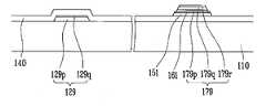
Translated fromKorean도 1은 본 발명의 한 실시예에 따른 박막 트랜지스터 표시판의 배치도이고,1 is a layout view of a thin film transistor array panel according to an exemplary embodiment of the present invention.
도 2 및 도 3은 각각 도 1의 박막 트랜지스터 표시판을 II-II' 선 및 III-III' 선을 따라 잘라 도시한 단면도이고,2 and 3 are cross-sectional views of the thin film transistor array panel of FIG. 1 taken along lines II-II 'and III-III', respectively.
도 4, 도 18 및 도 21은 본 발명의 한 실시예에 따른 박막 트랜지스터 표시판의 제조 방법을 차례로 도시한 배치도이고,4, 18 and 21 are layout views sequentially illustrating a method of manufacturing a thin film transistor array panel according to an exemplary embodiment of the present invention.
도 5 및 도 6은 도 4의 박막 트랜지스터 표시판을 V-V'선 및 VI-VI'선을 따라 잘라 도시한 단면도이고,5 and 6 are cross-sectional views of the thin film transistor array panel of FIG. 4 taken along the lines V-V 'and VI-VI'.
도 7 내지 도 17은 본 발명의 한 실시예에 따른 박막 트랜지스터 표시판의 제조 방법에 따라 차례로 도시한 단면도이고,7 to 17 are cross-sectional views sequentially shown according to a method of manufacturing a thin film transistor array panel according to an exemplary embodiment of the present invention.
도 19 및 도 20은 도 18의 박막 트랜지스터 표시판을 XVI-XVI'선 및 XVII-XVII'선을 따라 잘라 도시한 단면도이고,19 and 20 are cross-sectional views illustrating the thin film transistor array panel of FIG. 18 taken along lines XVI-XVI 'and XVII-XVII',
도 22 및 도 23는 도 21의 박막 트랜지스터 표시판을 XIX-XIX'선 및 XX-XX'선을 따라 잘라 도시한 단면도이다.22 and 23 are cross-sectional views of the thin film transistor array panel of FIG. 21 taken along lines XIX-XIX 'and XX-XX'.
본 발명은 박막 트랜지스터 표시판 및 그 제조 방법에 관한 것이다.The present invention relates to a thin film transistor array panel and a method of manufacturing the same.
액정 표시 장치(Liquid Crystal Display)는 현재 가장 널리 사용되고 있는 평판 표시 장치(Flat Panel Display) 중 하나로서, 전극이 형성되어 있는 두 장의 기판과 그 사이에 삽입되어 있는 액정층으로 이루어져, 전극에 전압을 인가하여 액정층의 액정 분자들을 재배열시킴으로써 투과되는 빛의 양을 조절하는 표시 장치이다.2. Description of the Related Art A liquid crystal display (LCD) is one of the most widely used flat panel displays, and is composed of two substrates on which electrodes are formed and a liquid crystal layer interposed therebetween. And rearranges the liquid crystal molecules in the liquid crystal layer to adjust the amount of light transmitted.
액정 표시 장치 중에서도 현재 주로 사용되는 것은 전계 생성 전극이 두 표시판에 각각 구비되어 있는 구조이다. 이 중에서도, 하나의 표시판(이하, '박막 트랜지스터 표시판'이라 함)에는 복수의 화소 전극이 행렬의 형태로 배열되어 있고 다른 표시판(이하, '공통 전극 표시판'이라 함)에는 하나의 공통 전극이 표시판 전면을 덮고 있는 구조의 형태가 주류이다. 이러한 액정 표시 장치에서의 화상의 표시는 각 화소 전극에 별도의 전압을 인가함으로써 이루어진다. 이를 위해서 화소 전극에 인가되는 전압을 스위칭하기 위한 삼단자 소자인 박막 트랜지스터를 각 화소 전극에 연결하고 이 박막 트랜지스터를 제어하기 위한 신호를 전달하는 게이트선(gate line)과 화소 전극에 인가될 전압을 전달하는 데이터선(data line)을 표시판에 형성한다.Among the liquid crystal display devices, the one currently used is a structure in which a field generating electrode is provided in each of the two display panels. Among these, a plurality of pixel electrodes are arranged in a matrix form on one display panel (hereinafter referred to as a 'thin film transistor display panel'), and one common electrode is used on another display panel (hereinafter, referred to as a 'common electrode display panel'). The shape of the structure covering the front is mainstream. The display of an image in such a liquid crystal display is performed by applying a separate voltage to each pixel electrode. To this end, a thin film transistor, which is a three-terminal element for switching the voltage applied to the pixel electrode, is connected to each pixel electrode, and a gate line for transmitting a signal for controlling the thin film transistor and a voltage to be applied to the pixel electrode are selected. A data line to transfer is formed on the display panel.
박막 트랜지스터는 게이트선(gate line)을 통하여 전달되는 주사 신호에 따라 데이터선(data line)을 통하여 전달되는 화상 신호를 화소 전극에 전달 또는 차단하는 스위칭 소자로서의 역할을 한다.The thin film transistor serves as a switching element that transfers or blocks an image signal transmitted through a data line to a pixel electrode according to a scan signal transmitted through a gate line.
박막 트랜지스터 표시판은 게이트선 및 데이터선을 포함하는 도전층, 반도체층 및 절연층을 포함한 복수의 박막을 포함하며, 각 박막은 별도의 마스크를 사용하여 패터닝된다.The thin film transistor array panel includes a plurality of thin films including a conductive layer including a gate line and a data line, a semiconductor layer, and an insulating layer, and each thin film is patterned using a separate mask.
하나의 마스크가 더 추가됨에 따라 감광막 도포, 노광, 현상 및 세정 공정을 반복해야 되므로 공정시간 및 비용이 현저하게 증가한다. 따라서, 가능한 마스크 수를 줄이는 것이 필요하다. 이에 따라, 데이터용 금속층과 반도체층을 하나의 마스크로 식각하는 방안이 제안되었다.As one more mask is added, the process time and cost are significantly increased since the photoresist coating, exposure, development, and cleaning processes must be repeated. Therefore, it is necessary to reduce the number of possible masks. Accordingly, a method of etching the data metal layer and the semiconductor layer with one mask has been proposed.
이 때 데이터용 금속층 하부 전면에 반도체층이 남게 되고, 데이터용 금속층 측면으로 반도체층이 돌출되는 현상이 발생한다. 따라서 광원에서 공급되는 빛에 노출되는 반도체층(151)의 면적이 넓어져서 광 누설 전류(photo leakage current)가 증가하게 되고, 이는 박막트랜지스터의 특성을 저하시켜 외부에서 잔상으로 시인될 수 있다. At this time, the semiconductor layer remains on the entire lower surface of the data metal layer, and the phenomenon that the semiconductor layer protrudes toward the side of the data metal layer occurs. Therefore, the area of the
따라서, 본 발명이 이루고자 하는 기술적 과제는 이러한 문제점을 해결하기 위한 것으로서, 데이터용 금속층 측면으로 돌출되는 반도체층의 길이를 감소시켜, 박막 트랜지스터 특성 및 잔상을 개선하는 것이다.Accordingly, the technical problem to be solved by the present invention is to solve this problem, and to reduce the length of the semiconductor layer protruding to the side of the data metal layer, thereby improving the thin film transistor characteristics and afterimage.
본 발명의 한 실시예에 따른 박막 트랜지스터 표시판의 제조방법은 기판 위에 게이트선을 형성하는 단계, 상기 게이트선 위에 게이트 절연막, 반도체층 및 저항성 접촉층을 형성하는 단계, 상기 저항성 접촉층 위에 도전층을 형성하는 단계, 상기 도전층 위에 제1 감광막 패턴을 형성하는 단계, 상기 제1 감광막 패턴을 식각 마스크로 하여 상기 도전층을 식각하는 단계, 상기 제1 감광막 패턴을 식각 마스크로 하여 상기 저항성 접촉층 및 상기 반도체층을 불소 함유 기체, 염소 함유 기체 및 산소(O2) 기체로 식각하는 단계, 상기 제1 감광막 패턴을 소정 두께만큼 제거하여 제2 감광막 패턴을 형성하는 단계, 상기 제2 감광막 패턴을 식각 마스크로 하여 상기 도전층을 식각하여 상기 저항성 접촉층의 일부를 노출시키는 단계를 포함하고, 상기 불소 함유 기체와 산소(O2) 기체의 유량비는 4:1 내지 1:1일 수 있다.A method of manufacturing a thin film transistor array panel according to an exemplary embodiment of the present invention includes forming a gate line on a substrate, forming a gate insulating layer, a semiconductor layer, and an ohmic contact layer on the gate line, and forming a conductive layer on the ohmic contact layer. Forming a first photoresist pattern on the conductive layer, etching the conductive layer using the first photoresist pattern as an etch mask, the ohmic contact layer using the first photoresist pattern as an etch mask, and Etching the semiconductor layer with a fluorine-containing gas, a chlorine-containing gas, and an oxygen (O2 ) gas, removing the first photoresist pattern by a predetermined thickness to form a second photoresist pattern, and etching the second photoresist pattern Etching the conductive layer using a mask to expose a portion of the ohmic contact layer, wherein the fluorine-containing group And oxygen (O2) flow rate of gas is from 4: 1 to 1: 1.
또한 상기 제1 감광막 패턴을 식각 마스크로 하여 상기 저항성 접촉층 및 상기 반도체층을 불소 함유 기체, 염소 함유 기체 및 산소(O2) 기체로 식각하는 단계에서 상기 게이트 절연막은 800 내지 2500 Å두께로 식각될 수 있다.In addition, the gate insulating layer may be etched to a thickness of 800 to 2500 μm by etching the ohmic contact layer and the semiconductor layer with a fluorine-containing gas, a chlorine-containing gas, and an oxygen (O2 ) gas by using the first photoresist pattern as an etching mask. Can be.
또한 상기 제1 감광막 패턴을 식각 마스크로 하여 상기 저항성 접촉층 및 상기 반도체층을 불소 함유 기체, 염소 함유 기체 및 산소(O2) 기체로 식각하는 단계 후, 남아있는 상기 게이트 절연막의 두께는 적어도 2000 Å 이상일 수 있다.In addition, after etching the ohmic contact layer and the semiconductor layer with a fluorine-containing gas, a chlorine-containing gas and an oxygen (O2 ) gas by using the first photoresist pattern as an etching mask, the thickness of the gate insulating film remaining is at least 2000. May be greater than or equal to
또한 상기 불소 함유 기체는 SF6또는CF4중 적어도 하나를 포함하고, 상기 염소 함유 기체는 염소 함유 기체는 HCl, Cl2, CCl4, BCl3 및 SiCl2H2중 적어도 하나를 포함할 수 있다.In addition, the fluorine-containing gas is SF6 or At least one of CF4 , and the chlorine-containing gas may include at least one of HCl, Cl2 , CCl4 , BCl3, and SiCl2 H2 .
또한 상기 불소 함유 기체는 SF6 일 수 있다.In addition, the fluorine-containing gas may be SF6 .
또한 상기 불소 함유 기체와 상기 산소 기체의 유량비는 2:1일 수 있다.In addition, the flow rate ratio of the fluorine-containing gas and the oxygen gas may be 2: 1.
또한 상기 염소 함유 기체는 HCl이며, 상기 HCl과 상기 불소 함유 기체의 유량비는 1:5일 수 있다.In addition, the chlorine-containing gas is HCl, the flow rate ratio of the HCl and the fluorine-containing gas may be 1: 5.
또한 상기 제1 감광막 패턴을 식각 마스크로 하여 상기 저항성 접촉층 및 상기 반도체층을 식각하는 단계는 100 내지 500mT의 압력하에 수행될 수 있다.The etching of the ohmic contact layer and the semiconductor layer using the first photoresist pattern as an etching mask may be performed under a pressure of 100 to 500 mT.
또한 상기 제1 감광막 패턴을 형성하는 단계는 제1 부분과 상기 제1 부분보다 두께가 얇은 제2 부분을 가지도록 형성할 수 있다.The forming of the first photoresist pattern may include forming a first portion and a second portion having a thickness thinner than that of the first portion.
또한 상기 도전층은 몰리브덴(Mo)을 포함하는 제1 도전층, 알루미늄(Al)을 포함하는 제2 도전층 및 몰리브덴(Mo)을 포함하는 제3 도전층일 수 있다.The conductive layer may be a first conductive layer including molybdenum (Mo), a second conductive layer including aluminum (Al), and a third conductive layer including molybdenum (Mo).
또한 상기 도전층을 식각하는 단계는 습식 식각으로 수행될 수 있다.In addition, the etching of the conductive layer may be performed by wet etching.
본 발명의 한 실시예에 따른 박막 트랜지스터 표시판은 기판, 상기 기판 위에 형성되어 있는 게이트선, 상기 게이트선 위에 형성되어 있는 게이트 절연막, 상기 게이트 절연막 위에 형성되어 있는 반도체층, 상기 반도체층 위에 형성되어 있으며 소스 전극을 포함하는 데이터선, 상기 반도체층 위에 형성되어 있으며 상기 소스 전극과 마주하는 드레인 전극, 상기 드레인 전극과 연결되어 있는 화소 전극을 포함하고, 상기 데이터선은 알루미늄(Al)을 포함하는 도전층과 상기 알루미늄(Al)을 포함하는 도전층의 하부 및 상부 중 적어도 하나에 형성되어 있는 몰리브덴(Mo)을 포함하는 도전층을 포함하며, 상기 반도체층은 상기 데이터선 및 상기 드레인 전극과 실질적으로 동일한 평면 모양을 가지고, 상기 반도체층 측면 돌출부 길이는 1.5um 이하일 수 있다.A thin film transistor array panel according to an exemplary embodiment of the present invention is formed on a substrate, a gate line formed on the substrate, a gate insulating film formed on the gate line, a semiconductor layer formed on the gate insulating film, and formed on the semiconductor layer. A data line including a source electrode, a drain electrode formed on the semiconductor layer and facing the source electrode, and a pixel electrode connected to the drain electrode, wherein the data line includes an aluminum (Al) layer. And a conductive layer including molybdenum (Mo) formed on at least one of a lower portion and an upper portion of the conductive layer including aluminum (Al), wherein the semiconductor layer is substantially the same as the data line and the drain electrode. It has a flat shape and the semiconductor layer side protrusion length may be 1.5um or less.
또한 상기 몰리브덴(Mo)을 포함하는 도전층은 순수 몰리브덴(Mo), 질화 몰리 브덴(MoN), 몰리브덴-니오븀(MoNb), 몰리브덴-바나듐(MoV), 몰리브덴-티타늄(MoTi), 몰리브덴-텅스텐(MoW) 중에서 선택된 어느 하나일 수 있다.In addition, the conductive layer including molybdenum (Mo) may be pure molybdenum (Mo), molybdenum nitride (MoN), molybdenum-niobium (MoNb), molybdenum-vanadium (MoV), molybdenum-titanium (MoTi), molybdenum-tungsten ( MoW) may be any one selected from.
또한 상기 알루미늄(Al)을 포함하는 도전층은 알루미늄-네오디뮴 합금(AlNd)일 수 있다.In addition, the conductive layer including aluminum (Al) may be an aluminum-neodymium alloy (AlNd).
또한 상기 데이터선은 몰리브덴을 포함하는 제1 도전층, 알루미늄을 포함하는 제2 도전층 및 몰리브덴을 포함하는 제3 도전층이 차례로 적층될 수 있다.In addition, the data line may include a first conductive layer including molybdenum, a second conductive layer including aluminum, and a third conductive layer including molybdenum.
또한 상기 게이트선은 알루미늄을 포함하는 도전층 및 몰리브덴을 포함하는 도전층을 포함할 수 있다.In addition, the gate line may include a conductive layer including aluminum and a conductive layer including molybdenum.
이하, 첨부한 도면을 참조하여 본 발명의 실시예에 대하여 본 발명이 속하는 기술분야에서 통상의 지식을 가진 자가 용이하게 실시할 수 있도록 상세히 설명한다. 그러나 본 발명은 여러 가지 상이한 형태로 구현될 수 있으며 여기에서 설명하는 실시예에 한정되지 않는다.Hereinafter, embodiments of the present invention will be described in detail with reference to the accompanying drawings so that those skilled in the art can easily carry out the present invention. The present invention may, however, be embodied in many different forms and should not be construed as limited to the embodiments set forth herein.
도면에서 여러 층 및 영역을 명확하게 표현하기 위하여 두께를 확대하여 나타내었다. 명세서 전체를 통하여 유사한 부분에 대해서는 동일한 도면 부호를 붙였다. 층, 막, 영역, 판 등의 부분이 다른 부분 "위에" 있다고 할 때, 이는 다른 부분 "바로 위에" 있는 경우 뿐만 아니라 그 중간에 또 다른 부분이 있는 경우도 포함한다. 반대로 어떤 부분이 다른 부분 "바로 위에" 있다고 할 때에는 중간에 다른 부분이 없는 것을 뜻한다.In the drawings, the thickness is enlarged to clearly represent the layers and regions. Like parts are designated with like reference numerals throughout the specification. Whenever a portion of a layer, film, region, plate, or the like is referred to as being "on" another portion, it includes not only the case where it is "directly on" another portion, but also the case where there is another portion in between. Conversely, when a part is "directly over" another part, it means that there is no other part in the middle.
그러면, 도 1 내지 도 3을 참고로 하여 본 발명의 한 실시예에 따른 박막 트랜지스터 표시판에 대하여 상세하게 설명한다.Next, the thin film transistor array panel according to the exemplary embodiment of the present invention will be described in detail with reference to FIGS. 1 to 3.
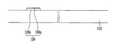
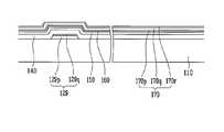
도 1은 본 발명의 한 실시예에 따른 박막 트랜지스터 표시판의 배치도이고, 도 2 및 도 3은 각각 도 1의 박막 트랜지스터 표시판을 II-II' 선 및 III-III' 선을 따라 잘라 도시한 단면도이다.1 is a layout view of a thin film transistor array panel according to an exemplary embodiment of the present invention, and FIGS. 2 and 3 are cross-sectional views illustrating the thin film transistor array panel of FIG. 1 taken along lines II-II 'and III-III', respectively. .
투명한 유리 또는 플라스틱 따위로 만들어진 절연 기판(110) 위에 복수의 게이트선(gate line)(121) 및 복수의 유지 전극선(storage electrode line)(131)이 형성되어 있다.A plurality of
게이트선(121)은 게이트 신호를 전달하며 주로 가로 방향으로 뻗어 있다. 각 게이트선(121)은 아래로 돌출한 복수의 게이트 전극(gate electrode)(124)과 다른 층 또는 외부 구동 회로와의 접속을 위하여 면적이 넓은 끝 부분(129)을 포함한다.The
유지 전극선(131)은 소정의 전압을 인가 받으며, 게이트선(121)과 거의 나란하게 뻗은 줄기선과 이로부터 갈라진 복수 쌍의 유지 전극(133a, 133b)을 포함한다. 그러나 유지 전극선(131)의 모양 및 배치는 여러 가지로 변형될 수 있다.The
게이트선(121) 및 유지 전극선(131)은 알루미늄(Al)이나 알루미늄 합금 등의 알루미늄 계열 금속을 포함하는 하부막(124p, 131p, 133ap, 133bp)과 몰리브덴(Mo)이나 몰리브덴 합금 등의 몰리브덴 계열 금속을 포함하는 상부막(124q, 131q, 133aq, 133bq)으로 이루어진다.The
도 2 및 도 3에서 게이트 전극(124) 및 유지 전극선(131)에 대하여 하부막은 영문자 p를, 상부막은 영문자 q를 도면 부호에 덧붙여 표기하였다.In FIG. 2 and FIG. 3, the lower film of the
게이트선(121) 및 유지 전극선(131) 위에는 질화규소(SiNx) 또는 산화규소 (SiOx) 따위로 만들어진 게이트 절연막(gate insulating layer)(140)이 형성되어 있다.A
게이트 절연막(140) 위에는 수소화 비정질 규소(hydrogenated amorphous silicon)(비정질 규소는 약칭 a-Si로 씀) 등으로 만들어진 복수의 선형 반도체(151)가 형성되어 있다. 선형 반도체(151)는 주로 세로 방향으로 뻗어 있으며, 게이트 전극(124)을 향하여 뻗어 나온 복수의 돌출부(projection)(154)를 포함한다. 선형 반도체(151)는 게이트선(121) 및 유지 전극선(131) 부근에서 너비가 넓어져 이들을 폭넓게 덮고 있다.A plurality of
반도체(151) 위에는 복수의 선형 및 섬형 저항성 접촉 부재(ohmic contact)(161, 165)가 형성되어 있다. 저항성 접촉 부재(161, 165)는 인(P) 따위의 n형 불순물이 고농도로 도핑되어 있는 n+ 수소화 비정질 규소 따위의 물질로 만들어지거나 실리사이드(silicide)로 만들어질 수 있다. 선형 저항성 접촉 부재(161)는 복수의 돌출부(163)를 가지고 있으며, 이 돌출부(163)와 섬형 저항성 접촉 부재(165)는 쌍을 이루어 반도체(151)의 돌출부(154) 위에 배치되어 있다.On the
저항성 접촉 부재(161, 165) 위에는 복수의 데이터선(data line)(171)과 복수의 드레인 전극(drain electrode)(175)이 형성되어 있다.A plurality of
데이터선(171)은 데이터 신호를 전달하며 주로 세로 방향으로 뻗어 게이트선(121)과 교차한다. 각 데이터선(171)은 게이트 전극(124)을 향하여 뻗은 복수의 소스 전극(source electrode)(173)과 다른 층 또는 외부 구동 회로와의 접속을 위하여 면적이 넓은 끝 부분(179)을 포함한다.The
드레인 전극(175)은 데이터선(171)과 분리되어 있고 게이트 전극(124)을 중심으로 소스 전극(173)과 마주 본다.The
하나의 게이트 전극(124), 하나의 소스 전극(173) 및 하나의 드레인 전극(175)은 반도체(151)의 돌출부(154)와 함께 하나의 박막 트랜지스터(thin film transistor, TFT)를 이루며, 박막 트랜지스터의 채널(channel)은 소스 전극(173)과 드레인 전극(175) 사이의 돌출부(154)에 형성된다.One
데이터선(171)은 하부막(171p, 175p), 중간막(171q, 175q) 및 상부막(171r, 175r)을 포함하는 삼중막 구조를 가진다. 하부막(171p, 175p)은 순수 몰리브덴 또는 질화 몰리브덴(MoN), 몰리브덴-니오븀(MoNb), 몰리브덴-바나듐(MoV), 몰리브덴-티타늄(MoTi), 몰리브덴-텅스텐(MoW) 따위의 몰리브덴 합금 등의 몰리브덴 계열의 금속으로 만들어지고, 중간막(171q, 175q)은 비저항이 낮은 알루미늄 또는 알루미늄-네오디뮴(AlNd) 따위의 알루미늄 합금으로 만들어지며, 상부막(171r, 175r)은 ITO나 IZO와의 접촉 특성이 우수한 순수 몰리브덴 또는 질화 몰리브덴(MoN), 몰리브덴-니오븀(MoNb), 몰리브덴-바나듐(MoV), 몰리브덴-티타늄(MoTi), 몰리브덴-텅스텐(MoW) 따위의 몰리브덴 합금 등의 몰리브덴 계열의 금속으로 만들어진다. 일반적으로 데이터선(171)의 측면은 기판면에 대하여 경사져 있으며, 경사각은 약 30ㅀ 내지 약 80ㅀ인 것이 바람직하다.The
도 2 및 도 3에서 소스 전극(173) 및 끝부분(179)을 포함하는 데이터선(171) 및 드레인 전극(175)에 대하여 하부막은 영문자 p를, 중간막은 영문자 q를, 상부막은 영문자 r을 도면 부호에 덧붙여 표기하였다.In FIGS. 2 and 3, the lower layer has an alphabet letter p, the middle layer has an alphabet letter q, and the upper layer has an alphabet letter r with respect to the
저항성 접촉 부재(161, 165)는 그 아래의 반도체(151)와 그 위의 데이터선(171) 및 드레인 전극(175) 사이에만 존재하며 이들 사이의 접촉 저항을 낮추어 준다.The
반도체층(151)은 박막 트랜지스터가 위치하는 돌출부(154)를 제외하면 데이터선(171), 드레인 전극(175) 및 그 하부의 저항성 접촉층(161, 163, 165)과 실질적으로 동일한 평면 형태를 가지고 있다. 즉, 선형 반도체층(151)은 데이터선(171) 및 드레인 전극(175)과 그 하부의 저항성 접촉층(161, 163, 165)의 아래에 모두 형성되어 있으며, 소스 전극(173)과 드레인 전극(175) 사이에는 노출되어 있다. 한편, 저항성 접촉 부재(161, 165) 및 반도체층(151)은 데이터 선(171), 드레인 전극(175)과 접하는 면을 기준면으로 했을 때, 데이터 선(171), 드레인 전극(175)으로부터 돌출되어 있다. 저항성 접촉 부재 및 반도체층이 데이터 선, 드레인 전극과 접하는 면을 기준면으로 하고, 데이터 선, 드레인 전극의 경계로부터 돌출되어 있는 부분을 이하에서는 '반도체층 측면 돌출부'라 하기로 한다.The
한편 저항성 접촉 부재와 반도체층의 측면은 일반적으로 기판면에 대하여 경사져 있으며, 경사각은 약 30ㅀ 내지 약 80ㅀ인 것이 바람직하다. 데이터 선(171), 드레인 전극(175)과 저항성 접촉 부재(161, 165)가 접하는 면을 제1 기준면으로 정하고, 제1 기준면 위에서 데이터 선(171), 드레인 전극(175)의 경계선을 제1 선으로 정한다.On the other hand, the side surfaces of the ohmic contact and the semiconductor layer are generally inclined with respect to the substrate surface, and the inclination angle is preferably about 30 kPa to about 80 kPa. A surface where the
한편, 반도체층과 게이트 절연막이 접하는 면을 제2 기준면으로 정하고, 제2기준면 위에서 반도체층의 경계선을 제2 선으로 정한다. 제2 선 상에서, 반도체층 측면에 접하는 가상의 접면(접선)을 생각하고, 가상의 접면과 제1 기준면이 접하는 선을 제3 선으로 정한다. 이 때 제1 선과 제3선의 거리를 반도체층 측면 돌출부의 길이로 정할 수 있다. 반도체층 측면 돌출부의 길이는 1.5um 이하이며, 돌출부의 길이가 작을수록 바람직하다.On the other hand, the surface where the semiconductor layer is in contact with the gate insulating film is defined as the second reference plane, and the boundary line of the semiconductor layer is defined as the second line on the second reference plane. On the second line, a virtual contact surface (tangential line) in contact with the side of the semiconductor layer is considered, and a line between the virtual contact surface and the first reference plane is defined as a third line. In this case, the distance between the first line and the third line may be determined as the length of the protrusion on the side surface of the semiconductor layer. The length of the semiconductor layer side protrusion is 1.5 um or less, and the smaller the length of the protrusion, the more preferable.
데이터선(171), 드레인 전극(175) 및 노출된 반도체(154) 부분 위에는 보호막(passivation layer)(180)이 형성되어 있다.A
보호막(180)은 질화규소나 산화규소 따위의 무기 절연물, 유기 절연물, 저유전율 절연물 따위로 만들어진다. 유기 절연물과 저유전율 절연물의 유전 상수는 4.0 이하인 것이 바람직하다. 보호막(180)에는 데이터선(171)의 끝 부분(179)과 드레인 전극(175)을 각각 드러내는 복수의 접촉 구멍(contact hole)(182, 185)이 형성되어 있으며, 보호막(180)과 게이트 절연막(140)에는 게이트선(121)의 끝 부분(129)을 드러내는 복수의 접촉 구멍(181), 유지 전극선(131) 일부를 드러내는 복수의 접촉 구멍(184)이 형성되어 있다.The
보호막(180) 위에는 복수의 화소 전극(pixel electrode)(191), 복수의 연결 다리(overpass)(84) 및 복수의 접촉 보조 부재(contact assistant)(81, 82)가 형성되어 있다. 이들은 ITO 또는 IZO 등의 투명한 도전 물질이나 알루미늄, 은 또는 그 합금 등의 반사성 금속으로 만들어질 수 있다.A plurality of
화소 전극(191)은 접촉 구멍(185)을 통하여 드레인 전극(175)과 물리적ㅇ전기적으로 연결되어 있으며, 드레인 전극(175)으로부터 데이터 전압을 인가 받는다. 데이터 전압이 인가된 화소 전극(191)은 공통 전압(common voltage)을 인가 받는 다른 표시판(도시하지 않음)의 공통 전극(common electrode)(도시하지 않음)과 함께 전기장을 생성함으로써 두 전극 사이의 액정층(도시하지 않음)의 액정 분자의 방향을 결정한다. 화소 전극(191)과 공통 전극은 축전기[이하 "액정 축전기(liquid crystal capacitor)"라 함]를 이루어 박막 트랜지스터가 턴 오프(turn-off)된 후에도 인가된 전압을 유지한다.The
접촉 보조 부재(81, 82)는 각각 접촉 구멍(181, 182)을 통하여 게이트선(121)의 끝 부분(129) 및 데이터선(171)의 끝 부분(179)과 연결된다.The contact
연결 다리(84)는 게이트선(121)을 가로지르며, 게이트선(121)을 사이에 두고 반대쪽에 위치하는 한 쌍의 접촉 구멍(184)을 통하여 유지 전극선(131)의 노출된 부분과 유지 전극(133b) 자유단의 노출된 끝 부분에 연결되어 있다.The connecting
그러면, 도 1 내지 도 3에 도시한 박막 트랜지스터 표시판을 제조하는 방법에 대하여 도 4 내지 도 23을 참조하여 상세하게 설명한다.Next, a method of manufacturing the thin film transistor array panel shown in FIGS. 1 to 3 will be described in detail with reference to FIGS. 4 to 23.
도 4, 도 18 및 도 21은 본 발명의 한 실시예에 따른 박막 트랜지스터 표시판의 제조 방법을 차례로 도시한 배치도이고, 도 5 및 도 6은 도 4의 박막 트랜지스터 표시판을 V-V'선 및 VI-VI'선을 따라 잘라 도시한 단면도이고, 도 7 내지 도 17은 본 발명의 한 실시예에 따른 박막 트랜지스터 표시판의 제조 방법에 따라 차례로 도시한 단면도이고, 도 19 및 도 20은 도 18의 박막 트랜지스터 표시판을 XVI-XVI'선 및 XVII-XVII'선을 따라 잘라 도시한 단면도이고, 도 22 및 도 23은 도 21의 박막 트랜지스터 표시판을 XIX-XIX'선 및 XX-XX'선을 따라 잘라 도시한 단면도이다.4, 18 and 21 are layout views sequentially illustrating a method of manufacturing a thin film transistor array panel according to an exemplary embodiment of the present invention, and FIGS. 5 and 6 are lines V-V ′ and VI of the thin film transistor array panel of FIG. 4. 7 to 17 are cross-sectional views sequentially showing the thin film transistor array panel according to the exemplary embodiment of the present invention, and FIGS. 19 and 20 are thin films of FIG. 18. Fig. 22 is a cross-sectional view of the transistor panel cut along the lines XVI-XVI 'and XVII-XVII', and Figs. 22 and 23 are cut out along the lines XIX-XIX 'and XX-XX' of Fig. 21. One cross section.
먼저, 도 4 내지 도 6에 도시한 바와 같이, 투명 유리 또는 플라스틱 따위로 만들어진 절연 기판(110) 위에 알루미늄-네오디뮴(AlNd)으로 만들어진 하부막 및 몰리브덴(Mo)계열의 금속으로 만들어진 하부막을 차례로 적층한다.First, as shown in FIGS. 4 to 6, a lower layer made of aluminum-neodymium (AlNd) and a lower layer made of molybdenum (Mo) -based metal are sequentially stacked on an insulating
그 다음, 하부막 및 상부막을 습식 식각(wet etching)하여 게이트 전극(124) 및 끝부분(129)을 포함하는 복수의 게이트선(121)과 유지 전극(133a, 133b)을 포함하는 복수의 유지 전극선(131)을 형성한다.Next, the plurality of
이어서, 도 7 및 도 8에 도시한 바와 같이, 게이트선(121) 및 유지 전극선(131) 위에 질화규소(SiNx) 따위로 만들어진 게이트 절연막(140), 불순물이 도핑되지 않은 진성 비정질 규소(a-Si)층(150) 및 불순물이 도핑된 비정질 규소(n+ a-Si)(160)층을 화학 기상 증착(plasma enhanced chemical vapor deposition, PECVD) 으로 형성한다. 진성 비정질 규소층(150)은 수소화 비정질 규소(hydrogenated amorphous silicon) 등으로 형성하며 불순물이 도핑된 비정질 규소층(160)은 인(P) 등의 n형 불순물이 고농도로 도핑된 비정질 규소 또는 실리사이드로 형성한다.Subsequently, as shown in FIGS. 7 and 8, the
연속적으로, 불순물이 도핑된 비정질 규소층(160) 위에 몰리브덴 계열의 금속으로 만들어진 하부 몰리브덴층(170p), 알루미늄 계열의 금속으로 만들어진 알루미늄층(170q) 및 몰리브덴 계열의 금속으로 만들어진 상부 몰리브덴층(170r)을 포함하는 데이터 금속층(170)을 스퍼터링으로 차례로 적층한다.Subsequently, the
그 다음, 도 9 및 도 10에 도시한 바와 같이, 상부 몰리브덴층(170r) 위에 감광막을 형성한 후 노광 및 현상하여 서로 다른 두께를 가지는 감광막 패턴(52, 54)을 형성한다.9 and 10, a photoresist film is formed on the
여기서, 설명의 편의상, 배선이 형성될 부분의 데이터 금속층(170), 불순물이 도핑된 비정질 규소층(160), 진성 비정질 규소층(150)을 배선 부분(A)이라 하고, 게이트 전극(124) 위에 채널이 형성되는 부분을 채널 부분(B)이라 하고, 배선 부분(A) 및 채널 부분(B)을 제외한 영역을 나머지 부분(C)이라 한다.Here, for convenience of description, the
감광막 패턴(52, 54) 중에서 배선 부분(A)에 위치한 제1 부분(52)은 채널 부분(B)에 위치한 제2 부분(54)보다 두껍게 형성하며, 나머지 부분(C)의 감광막은 모두 제거한다. 이 때, 제1 부분(52)의 두께와 제2 부분(54)의 두께의 비(ratio)는 후술할 식각 공정에서의 공정 조건에 따라 다르게 하여야 하되, 제2 부분(54)의 두께를 제1 부분(52)의 두께의 1/2 이하로 하는 것이 바람직하다. Among the
이와 같이, 위치에 따라 감광막의 두께를 다르게 형성하는 방법에는 여러 가지가 있을 수 있는데, 노광 마스크에 투명 영역(transparent area)과 차광 영역(light blocking area) 뿐 아니라 반투명 영역(semi-transparent area)을 두는 것이 그 예이다.As described above, there may be various methods of forming the thickness of the photoresist film differently according to the position. A semi-transparent area as well as a transparent area and a light blocking area may be formed in the exposure mask. For example.
이어서, 도 11 및 도 12에 도시한 바와 같이, 감광막 패턴의 제1 부분(52)을 이용하여 나머지 부분(C)에 노출되어 있는 데이터 금속층(170)을 습식 식각(wet etching)으로 제거한다. 11 and 12, the
그 다음, 도 13 및 도 14에 도시된 바와 같이, 감광막 패턴의 제1 부분(52)을 이용하여 나머지 부분(C)에 남아있는 불순물이 도핑된 비정질 규소층(160) 및 진성 비정질 규소층(150)을 건식 식각(dry etching)한다.Next, as shown in FIGS. 13 and 14, the
이 때, 건식 식각용 기체로는 불소 함유 기체, 염소 함유 기체 및 산소 기체 를 이용한다.At this time, as the dry etching gas, fluorine-containing gas, chlorine-containing gas and oxygen gas are used.
불소 함유 기체는 SF6 또는 CF4 등 불소 원자(F)가 포함된 기체일 수 있다.The fluorine-containing gas may be a gas containing a fluorine atom (F) such as SF6 or CF4 .
염소 함유 기체는 Cl2, HCl, BCl3, CCl4, SiCl2H2등 염소 원자(Cl)가 포함된 기체일 수 있다. 한편 불소 함유 기체, 염소 함유 기체와 함께 산소 기체(O2)가 공급된다.The chlorine-containing gas may be a gas containing a chlorine atom (Cl) such as Cl2 , HCl, BCl3 , CCl4 , SiCl2 H2, and the like. On the other hand, oxygen gas (O2 ) is supplied together with the fluorine-containing gas and the chlorine-containing gas.
이 때 식각 압력은 사용되는 장비, 장비 모드 및 기판의 크기에 따라 적절하게 선택될 수 있다. 예를 들면, PE mode의 장비에서는 약 100 내지 500mT에서 수행될 수 있다. 보다 바람직하게는 200mT에서 수행될 수 있다. 또한 RIE mode의 장비에서는 약 5 내지 30mT의 범위에서 수행될 수 있다.At this time, the etching pressure may be appropriately selected depending on the size of the equipment, the equipment mode and the substrate used. For example, in the PE mode equipment may be performed at about 100 to 500mT. More preferably it may be carried out at 200mT. In addition, the RIE mode of the equipment may be performed in the range of about 5 to 30mT.
SF6, HCl 및 O2가 함께 사용되는 경우, SF6 와 O2의 유량비(flow ratio)는 4:1 내지 1:1인 것이 바람직하다. 보다 바람직하게는 SF6 와 O2의 유량비는 2:1인 것이 바람직하다. 이 때, SF6와 HCl의 유량비는 1:1 내지 5:1의 범위에서 사용될 수 있으나, 5:1로 유지하는 것이 바람직하다.When SF6, HCl and O2 are used together, the flow ratio of SF6 and O2 is preferably 4: 1 to 1: 1. More preferably, the flow rate ratio of SF6 and O2 is 2: 1. At this time, the flow rate ratio of SF6 and HCl may be used in the range of 1: 1 to 5: 1, but is preferably maintained at 5: 1.
상기 비율로 비정질 규소층(160) 및 진성 비정질 규소층(150)을 건식 식각(dry etching)하면 박막 트랜지스터의 특성이 개선될 수 있다.Dry etching the
전술한 바와 같이 데이터 금속 패턴(171, 173, 179)과 진성 비정질 규소층(150)을 동일한 감광막 패턴을 이용하여 식각하는 경우, 소스 전극(173) 및 끝부분(179)을 포함하는 데이터선(171)과 돌출부(154)를 포함하는 반도체층(151)이 실질 적으로 동일한 평면 모양을 가진다. 그렇지만 결과적으로 액정 표시 장치에 형성된 반도체층(151)은 데이터 선(171), 드레인 전극(175)과 접하는 면을 기준면으로 했을 때, 데이터 선(171), 드레인 전극(175)으로부터 돌출된 반도체층 측면 돌출부를 갖는다.As described above, when the
이에 따라 본 발명에서는 감광막 패턴의 제1 부분(52)을 이용하여 나머지 부분(C)에 남아있는 불순물이 도핑된 비정질 규소층(160) 및 진성 비정질 규소층(150)을 건식 식각(dry etching)하는 단계에서, 불소 함유 기체, 염소 함유 기체 및 산소 기체의 유량비를 소정 범위로 조절함으로써 반도체층 측면 돌출부의 길이를 감소시켰다.Accordingly, in the present invention, dry etching is performed on the
이어서, 에치백(etch back) 공정을 이용하여 채널 부분(B)에 존재하는 감광막 패턴의 제2 부분(54)을 제거한다. 이 때, 감광막 패턴의 제1 부분(52)의 두께도 어느 정도 얇아진다.Subsequently, the
그 다음, 도 15 및 도 16에 도시한 바와 같이, 감광막 패턴의 제2 부분(54)이 제거된 제1 부분(52)을 이용하여 습식 식각하여, 데이터 금속 패턴(174)을 소스 전극(173)과 드레인 전극(175)으로 분리한다. 그 후 소스 전극(173)과 드레인 전극(175) 사이의 채널 영역에 불순물이 도핑된 비정질 규소 패턴(164)을 노출시킨다.15 and 16, wet etching is performed using the
이 때 감광막 패턴의 아래에 있는 데이터 금속 패턴(174)의 측면이 습식 식각액에 노출되므로, 데이터 금속 패턴(174)의 측면도 함께 식각된다. 따라서 반도체 층(151)이 데이터 선(171), 드레인 전극(175)과 접하는 면을 기준으로 돌출되는 반도체층 측면 돌출부가 생긴다. 다만 본 발명에서는 진성 비정질 규소층 및 비정 질 규소층을 건식 식각 하는 단계에서 식각 기체의 비율을 조절하여, 먼저 진성 비정질 규소층 및 비정질 규소층을 더욱 안쪽으로 식각함으로써, 결과적으로 반도체층 측면 돌출부를 감소시킬 수 있다.At this time, since the side surface of the
그 다음, 감광막 패턴의 제1 부분(52)을 식각 마스크로 하여 채널 영역에 위치한 불순물이 도핑된 비정질 규소 패턴(164)을 건식 식각한다. Subsequently, the
표 1은 본 발명의 한 실시예에서 사용된 불소 함유 기체와 산소 기체의 유량비를 다르게 하여 비정질 규소층 및 진성 비정질 규소층을 식각하는 경우에 반도체층 측면 돌출부 및 잔류 게이트 절연층의 두께를 나타내는 시험예이다.Table 1 is a test showing the thickness of the semiconductor layer side protrusion and the remaining gate insulating layer when etching the amorphous silicon layer and the intrinsic amorphous silicon layer by varying the flow rate ratio of the fluorine-containing gas and the oxygen gas used in one embodiment of the present invention. Yes.
한편 도 17은 사용된 건식 식각 기체인 SF6, HCl 및 O2의 유량이 각각 100sccm, 20sccm 및 50sccm인 경우에 형성된 반도체층 측면 돌출부의 길이를 측정한 결과이다. 도 17을 참조하면, 초기에 형성된 게이트 절연층의 두께는 4500Å이었으나, 잔류 게이트 절연층의 두께는 얇아졌음을 알 수 있다.17 is a result of measuring the lengths of the protrusions of the side surfaces of the semiconductor layer formed when the flow rates of SF6 , HCl, and O2 , which are used dry etching gases, are 100 sccm, 20 sccm, and 50 sccm, respectively. Referring to FIG. 17, it can be seen that the thickness of the gate insulating layer formed initially was 4500 kPa, but the thickness of the remaining gate insulating layer was thin.
각 시험예에서 HCl 공급량은 20sccm으로 유지하였다. 또한 PE mode의 장비에서 200mT, 400W 조건하에서 시험하였다. 그리고 불소 함유 기체인 SF6의 유량을 100sccm으로 유지하고, 산소 기체(O2)의 유량을 25sccm 에서 100sccm 까지 소정비율로 조절하여 유량을 공급하였다.The HCl feed was maintained at 20 sccm in each test example. It was also tested under 200mT, 400W conditions in PE mode equipment. The flow rate of SF6 , which is a fluorine-containing gas, was maintained at 100 sccm, and the flow rate of the oxygen gas (O2 ) was adjusted at a predetermined ratio from 25 sccm to 100 sccm.

표 1에서 보는 바와 같이, SF6 : O2의 유량비가 각각 4:1 내지 1:1인 경우, 반도체층 측면 돌출부 길이가 감소하였다. 따라서 잔상 개선 효과가 나타날 것으로 생각된다. 건식 식각 기체에 함유된 산소의 비율이 높아질수록 반도체층 측면 돌출부의 길이가 감소하는 경향을 보였으나, 잔류 게이트 절연층의 두께는 얇아지는 경향을 보였다. SF6 : O2의 유량비가 각각 4:1 내지 1:1인 경우, 1540 내지 2440Å의 게이트 절연막이 식각된다. 그렇지만 하부 게이트 절연막 잔류량의 두께는 2000Å 이상 유지된다. 만약 하부 게이트 절연막 잔류량의 두께가 2000Å이하인 경우, 게이트 선과 데이터 선간의 단락이 발생될 가능성이 있다.As shown in Table 1, when the flow rate ratio of SF6 : 02 was 4: 1 to 1: 1, respectively, the length of the semiconductor layer side protrusion was reduced. Therefore, the afterimage improvement effect is expected. As the ratio of oxygen contained in the dry etching gas increases, the length of the protrusion of the side surface of the semiconductor layer tends to decrease, but the thickness of the remaining gate insulating layer tends to decrease. When the flow rate ratio of SF6 : O2 is 4: 1 to 1: 1, the gate insulating film of 1540 to 2440 Pa is etched. However, the thickness of the remaining amount of the lower gate insulating film is maintained at 2000 GPa or more. If the thickness of the lower gate insulating film remaining amount is 2000 m or less, there is a possibility that a short circuit between the gate line and the data line occurs.
일반적으로 산소 기체는 등방성 식각 경향이 있으며, 산소 기체를 많이 함유할수록 기판과 평행한 방향으로의 식각 비율(etch rate)이 증가된다. 따라서 건식 식각 시 사용하는 산소 기체 함량을 늘이면, 비정질 규소층(160) 및 진성 비정질 규소층(150)이 데이터 금속층(170)을 기준으로 더욱 안쪽으로 식각된다. 따라서 결과적으로 액정 표시 장치에 형성된 반도체층 측면 돌출부의 길이를 감소시킬 수 있다. 이 때 염소 함유 기체의 비율은 다양하게 사용될 수 있으나, 산소 기체로 인한 등방성 식각 경향의 효과를 높이기 위하여, 불소 함유 기체와 염소 함유 기체의 유량비는 1:1 내지 5:1의 범위에서 사용되는 것이 좋다. 본 발명의 한 실시예에서는 불소 함유 기체와 염소 함유 기체의 유량비는 5:1로 사용하여 시험하였다.In general, oxygen gas tends to be isotropic, and the more oxygen gas is contained, the more the etch rate in the direction parallel to the substrate is increased. Therefore, when the oxygen gas content used in the dry etching is increased, the
한편 불소 함유 기체, 염소 함유 기체 및 산소 기체를 혼합하여 사용하는 경우 불소 함유 기체와 산소 기체의 유량비는 4:1 내지 1:1의 범위 내에서 시간에 따라 변화시킬 수 있다.On the other hand, when using a mixture of fluorine-containing gas, chlorine-containing gas and oxygen gas, the flow rate ratio of the fluorine-containing gas and oxygen gas can be changed over time in the range of 4: 1 to 1: 1.
그 후, 도 18, 19 및 도 20에 도시한 바와 같이, 감광막 패턴(52)을 제거한다.Thereafter, as shown in Figs. 18, 19 and 20, the
그 다음, 도 21 내지 도 23에 도시한 바와 같이, 데이터선(171) 및 드레인 전극(175)에 의해 가려지지 않는 반도체의 돌출부(154)를 덮도록 보호막(180)을 형성한다.Next, as shown in FIGS. 21 through 23, the
이어서, 보호막(180)을 사진 공정으로 식각하여 복수의 접촉 구멍(181, 182, 184, 185)을 형성한다.Subsequently, the
마지막으로, 도 1 내지 도 3에 도시한 바와 같이, 보호막(180) 위에 ITO 또는 IZO 따위의 투명한 도전 물질을 스퍼터링으로 증착한 후 패터닝하여, 화소 전극(191), 접촉 보조 부재(81, 82) 및 연결 다리(84)를 형성한다.Finally, as shown in FIGS. 1 to 3, a transparent conductive material such as ITO or IZO is deposited on the
이상에서 본 발명의 바람직한 실시예들에 대하여 상세하게 설명하였지만 본 발명의 권리범위는 이에 한정되는 것은 아니고 다음의 청구범위에서 정의하고 있는 본 발명의 기본 개념을 이용한 당업자의 여러 변형 및 개량 형태 또한 본 발명의 권리범위에 속하는 것이다. 또한 본 발명의 실시예는 4매 공정을 기준으로 설명하였으나, 본 발명은 3매 공정 등에도 사용될 수 있음은 물론이다.While the present invention has been particularly shown and described with reference to exemplary embodiments thereof, it is to be understood that the invention is not limited to the disclosed exemplary embodiments, And falls within the scope of the invention. In addition, although the embodiment of the present invention has been described based on the four-sheet process, the present invention can be used in the three-sheet process and the like.
상기와 같이, 데이터선을 알루미늄층 및 몰리브덴층을 포함하는 다층막으로 형성하고 소정 유량비를 가지는 식각 기체로 저항성 접촉층 및 상기 반도체층을 식각하여 박막 트랜지스터 특성을 개선시키고 잔상 발생을 방지할 수 있다.As described above, the resistive contact layer and the semiconductor layer may be etched with an etching gas having a predetermined flow rate and the data line is formed of a multilayer film including an aluminum layer and a molybdenum layer, thereby improving thin film transistor characteristics and preventing afterimage generation.
Claims (19)
Translated fromKoreanPriority Applications (3)
| Application Number | Priority Date | Filing Date | Title |
|---|---|---|---|
| KR1020060008878AKR101251995B1 (en) | 2006-01-27 | 2006-01-27 | Thin film transistor array panel and method for manufacturing the same |
| US11/544,987US7758760B2 (en) | 2006-01-27 | 2006-10-06 | Thin film transistor array panel and method of manufacturing the same |
| CN2006101428036ACN101009250B (en) | 2006-01-27 | 2006-10-26 | Thin film transistor array panel and method of manufacturing the same |
Applications Claiming Priority (1)
| Application Number | Priority Date | Filing Date | Title |
|---|---|---|---|
| KR1020060008878AKR101251995B1 (en) | 2006-01-27 | 2006-01-27 | Thin film transistor array panel and method for manufacturing the same |
Publications (2)
| Publication Number | Publication Date |
|---|---|
| KR20070078532A KR20070078532A (en) | 2007-08-01 |
| KR101251995B1true KR101251995B1 (en) | 2013-04-08 |
Family
ID=38322481
Family Applications (1)
| Application Number | Title | Priority Date | Filing Date |
|---|---|---|---|
| KR1020060008878AActiveKR101251995B1 (en) | 2006-01-27 | 2006-01-27 | Thin film transistor array panel and method for manufacturing the same |
Country Status (3)
| Country | Link |
|---|---|
| US (1) | US7758760B2 (en) |
| KR (1) | KR101251995B1 (en) |
| CN (1) | CN101009250B (en) |
Families Citing this family (7)
| Publication number | Priority date | Publication date | Assignee | Title |
|---|---|---|---|---|
| CN101566766A (en)* | 2008-04-23 | 2009-10-28 | 深超光电(深圳)有限公司 | Picture element layout structure and manufacturing method thereof |
| TWI749283B (en) | 2008-11-28 | 2021-12-11 | 日商半導體能源研究所股份有限公司 | Liquid crystal display device |
| JP6070073B2 (en)* | 2012-10-31 | 2017-02-01 | 凸版印刷株式会社 | Thin film transistor array |
| US20140199833A1 (en)* | 2013-01-11 | 2014-07-17 | Applied Materials, Inc. | Methods for performing a via reveal etching process for forming through-silicon vias in a substrate |
| CN106653771B (en) | 2016-12-30 | 2019-06-18 | 惠科股份有限公司 | Display panel and manufacturing process |
| CN106653772B (en)* | 2016-12-30 | 2019-10-01 | 惠科股份有限公司 | A display panel and its manufacturing process |
| CN207082531U (en)* | 2017-08-21 | 2018-03-09 | 京东方科技集团股份有限公司 | Array substrate and display device |
Citations (2)
| Publication number | Priority date | Publication date | Assignee | Title |
|---|---|---|---|---|
| KR20020036013A (en)* | 2000-11-07 | 2002-05-16 | 윤종용 | Thin film transistor array panel, method for manufacturing the same, device testing the same |
| KR20050019492A (en)* | 2003-08-19 | 2005-03-03 | 삼성전자주식회사 | Thin film transistor array panel and manufacturing method thereof |
Family Cites Families (22)
| Publication number | Priority date | Publication date | Assignee | Title |
|---|---|---|---|---|
| JPH08172202A (en)* | 1994-12-20 | 1996-07-02 | Sharp Corp | Thin film transistor and manufacturing method thereof |
| JP3947515B2 (en) | 1997-05-27 | 2007-07-25 | 三菱電機株式会社 | Contact hole forming method of active matrix substrate |
| US6054392A (en)* | 1997-05-27 | 2000-04-25 | Mitsubishi Denki Kabushiki Kaisha | Active matrix substrate and method of forming a contact hole in the same |
| KR100261974B1 (en) | 1997-08-28 | 2000-07-15 | 구본준 | Structure of lcd panel and manufacturing method thereof |
| US6432830B1 (en)* | 1998-05-15 | 2002-08-13 | Applied Materials, Inc. | Semiconductor fabrication process |
| US6583065B1 (en)* | 1999-08-03 | 2003-06-24 | Applied Materials Inc. | Sidewall polymer forming gas additives for etching processes |
| JP3074274B1 (en) | 1999-10-13 | 2000-08-07 | 財団法人工業技術研究院 | Method of manufacturing TFT for liquid crystal display |
| KR100613767B1 (en) | 1999-11-10 | 2006-08-18 | 비오이 하이디스 테크놀로지 주식회사 | Method of manufacturing thin film transistor liquid crystal display device |
| KR100603841B1 (en) | 2000-02-18 | 2006-07-24 | 엘지.필립스 엘시디 주식회사 | Reflective Liquid Crystal Display Manufacturing Method |
| KR100720091B1 (en) | 2000-10-31 | 2007-05-18 | 삼성전자주식회사 | Thin film transistor substrate and its manufacturing method |
| KR20020055787A (en) | 2000-12-29 | 2002-07-10 | 구본준, 론 위라하디락사 | Array Panel used for a Liquid Crystal Display and method for fabricating the same |
| KR20030027302A (en)* | 2001-09-28 | 2003-04-07 | 삼성전자주식회사 | A thin film transistor substrate of using insulating layers having law dielectric constant and a method of manufacturing the same |
| US7071037B2 (en)* | 2001-03-06 | 2006-07-04 | Semiconductor Energy Laboratory Co., Ltd. | Semiconductor device and manufacturing method thereof |
| JP4267242B2 (en) | 2001-03-06 | 2009-05-27 | 株式会社半導体エネルギー研究所 | Semiconductor device and manufacturing method thereof |
| JP2002268085A (en) | 2001-03-09 | 2002-09-18 | Matsushita Electric Ind Co Ltd | Manufacturing method and manufacturing apparatus for liquid crystal display device |
| JP2003068755A (en) | 2001-08-22 | 2003-03-07 | Sharp Corp | Thin film transistor and method of manufacturing the same |
| TWI232991B (en) | 2002-11-15 | 2005-05-21 | Nec Lcd Technologies Ltd | Method for manufacturing an LCD device |
| KR100925458B1 (en)* | 2003-01-17 | 2009-11-06 | 삼성전자주식회사 | Thin film transistor array panel and manufacturing method thereof |
| KR20040091484A (en) | 2003-04-22 | 2004-10-28 | 삼성전자주식회사 | Manufacturing method of thin film transistor array panel |
| KR100542986B1 (en)* | 2003-04-29 | 2006-01-20 | 삼성에스디아이 주식회사 | Thin film transistor, method for manufacturing thin film transistor and display device using same |
| JP4932150B2 (en) | 2003-10-21 | 2012-05-16 | 株式会社半導体エネルギー研究所 | Manufacturing method of semiconductor element |
| US7172913B2 (en) | 2004-03-19 | 2007-02-06 | Samsung Electronics Co., Ltd. | Thin film transistor array panel and manufacturing method thereof |
- 2006
- 2006-01-27KRKR1020060008878Apatent/KR101251995B1/enactiveActive
- 2006-10-06USUS11/544,987patent/US7758760B2/enactiveActive
- 2006-10-26CNCN2006101428036Apatent/CN101009250B/enactiveActive
Patent Citations (2)
| Publication number | Priority date | Publication date | Assignee | Title |
|---|---|---|---|---|
| KR20020036013A (en)* | 2000-11-07 | 2002-05-16 | 윤종용 | Thin film transistor array panel, method for manufacturing the same, device testing the same |
| KR20050019492A (en)* | 2003-08-19 | 2005-03-03 | 삼성전자주식회사 | Thin film transistor array panel and manufacturing method thereof |
Also Published As
| Publication number | Publication date |
|---|---|
| CN101009250B (en) | 2011-11-09 |
| US20070178413A1 (en) | 2007-08-02 |
| KR20070078532A (en) | 2007-08-01 |
| CN101009250A (en) | 2007-08-01 |
| US7758760B2 (en) | 2010-07-20 |
Similar Documents
| Publication | Publication Date | Title |
|---|---|---|
| JP5156203B2 (en) | Thin film transistor array panel and manufacturing method thereof | |
| KR101326128B1 (en) | Wire for display device, etchant, thin film transistor array panel and method for manufacturing the same | |
| KR101251995B1 (en) | Thin film transistor array panel and method for manufacturing the same | |
| KR101229277B1 (en) | Method of manufacturing thin film transistor substrate | |
| KR20100019233A (en) | Thin film transistor substrate and method of fabricating the same | |
| KR20170087568A (en) | Liquid crystal display device and method for fabricating the same | |
| KR20080019398A (en) | Thin film transistor array panel and manufacturing method thereof | |
| KR101171187B1 (en) | Thin film transistor array panel, manufacturing method thereof, and liquid crystal display including the same | |
| KR20070092455A (en) | Display device and manufacturing method thereof | |
| KR20080034598A (en) | Method of manufacturing thin film transistor array panel | |
| KR101282404B1 (en) | Method of manufacturing liquid crystal display | |
| KR101152139B1 (en) | Cleaning material for display device and method for manufacturing thin film transistor array panel using the same | |
| KR20080030798A (en) | Method of manufacturing thin film transistor array panel | |
| US10128274B2 (en) | Thin film transistor array panel and a method for manufacturing the same | |
| KR20080030761A (en) | Method of manufacturing thin film transistor array panel | |
| KR20070008869A (en) | Thin film transistor array panel and manufacturing method thereof | |
| KR20080057779A (en) | Method of manufacturing thin film transistor substrate | |
| KR20080051483A (en) | Method of manufacturing thin film transistor substrate | |
| KR100930573B1 (en) | Thin film transistor manufacturing method and display device manufacturing method using same | |
| JPH11274514A (en) | Method for manufacturing thin film transistor | |
| CN113345966A (en) | Thin film transistor and method of manufacturing the same | |
| KR20070046321A (en) | Thin film transistor array panel and manufacturing method thereof | |
| KR20150079258A (en) | Thin film transistor array panel | |
| KR20080049985A (en) | Liquid Crystal Display and Manufacturing Method Thereof | |
| KR20070039758A (en) | Method of manufacturing thin film transistor array panel |
Legal Events
| Date | Code | Title | Description |
|---|---|---|---|
| PA0109 | Patent application | Patent event code:PA01091R01D Comment text:Patent Application Patent event date:20060127 | |
| AMND | Amendment | ||
| PG1501 | Laying open of application | ||
| A201 | Request for examination | ||
| PA0201 | Request for examination | Patent event code:PA02012R01D Patent event date:20110127 Comment text:Request for Examination of Application Patent event code:PA02011R01I Patent event date:20060127 Comment text:Patent Application | |
| E902 | Notification of reason for refusal | ||
| PE0902 | Notice of grounds for rejection | Comment text:Notification of reason for refusal Patent event date:20120612 Patent event code:PE09021S01D | |
| AMND | Amendment | ||
| N231 | Notification of change of applicant | ||
| PN2301 | Change of applicant | Patent event date:20120913 Comment text:Notification of Change of Applicant Patent event code:PN23011R01D | |
| E601 | Decision to refuse application | ||
| PE0601 | Decision on rejection of patent | Patent event date:20121102 Comment text:Decision to Refuse Application Patent event code:PE06012S01D Patent event date:20120612 Comment text:Notification of reason for refusal Patent event code:PE06011S01I | |
| AMND | Amendment | ||
| J201 | Request for trial against refusal decision | ||
| PJ0201 | Trial against decision of rejection | Patent event date:20121121 Comment text:Request for Trial against Decision on Refusal Patent event code:PJ02012R01D Patent event date:20121102 Comment text:Decision to Refuse Application Patent event code:PJ02011S01I Appeal kind category:Appeal against decision to decline refusal Decision date:20130103 Appeal identifier:2012101009728 Request date:20121121 | |
| PB0901 | Examination by re-examination before a trial | Comment text:Amendment to Specification, etc. Patent event date:20121121 Patent event code:PB09011R02I Comment text:Request for Trial against Decision on Refusal Patent event date:20121121 Patent event code:PB09011R01I Comment text:Amendment to Specification, etc. Patent event date:20120806 Patent event code:PB09011R02I Comment text:Amendment to Specification, etc. Patent event date:20060328 Patent event code:PB09011R02I | |
| B701 | Decision to grant | ||
| PB0701 | Decision of registration after re-examination before a trial | Patent event date:20130114 Comment text:Decision to Grant Registration Patent event code:PB07012S01D Patent event date:20121226 Comment text:Transfer of Trial File for Re-examination before a Trial Patent event code:PB07011S01I | |
| GRNT | Written decision to grant | ||
| PR0701 | Registration of establishment | Comment text:Registration of Establishment Patent event date:20130402 Patent event code:PR07011E01D | |
| PR1002 | Payment of registration fee | Payment date:20130402 End annual number:3 Start annual number:1 | |
| PG1601 | Publication of registration | ||
| FPAY | Annual fee payment | Payment date:20160329 Year of fee payment:4 | |
| PR1001 | Payment of annual fee | Payment date:20160329 Start annual number:4 End annual number:4 | |
| FPAY | Annual fee payment | Payment date:20180403 Year of fee payment:6 | |
| PR1001 | Payment of annual fee | Payment date:20180403 Start annual number:6 End annual number:6 | |
| FPAY | Annual fee payment | Payment date:20190401 Year of fee payment:7 | |
| PR1001 | Payment of annual fee | Payment date:20190401 Start annual number:7 End annual number:7 | |
| PR1001 | Payment of annual fee | Payment date:20200402 Start annual number:8 End annual number:8 | |
| PR1001 | Payment of annual fee | Payment date:20210401 Start annual number:9 End annual number:9 | |
| PR1001 | Payment of annual fee | Payment date:20220323 Start annual number:10 End annual number:10 | |
| PR1001 | Payment of annual fee | Payment date:20230328 Start annual number:11 End annual number:11 |