KR101249763B1 - LED Display Apparatus - Google Patents
LED Display ApparatusDownload PDFInfo
- Publication number
- KR101249763B1 KR101249763B1KR1020100084618AKR20100084618AKR101249763B1KR 101249763 B1KR101249763 B1KR 101249763B1KR 1020100084618 AKR1020100084618 AKR 1020100084618AKR 20100084618 AKR20100084618 AKR 20100084618AKR 101249763 B1KR101249763 B1KR 101249763B1
- Authority
- KR
- South Korea
- Prior art keywords
- led
- display surface
- driving chip
- copper foil
- main substrate
- Prior art date
- Legal status (The legal status is an assumption and is not a legal conclusion. Google has not performed a legal analysis and makes no representation as to the accuracy of the status listed.)
- Expired - Fee Related
Links
Images


Classifications
- G—PHYSICS
- G09—EDUCATION; CRYPTOGRAPHY; DISPLAY; ADVERTISING; SEALS
- G09F—DISPLAYING; ADVERTISING; SIGNS; LABELS OR NAME-PLATES; SEALS
- G09F9/00—Indicating arrangements for variable information in which the information is built-up on a support by selection or combination of individual elements
- G09F9/30—Indicating arrangements for variable information in which the information is built-up on a support by selection or combination of individual elements in which the desired character or characters are formed by combining individual elements
- G09F9/33—Indicating arrangements for variable information in which the information is built-up on a support by selection or combination of individual elements in which the desired character or characters are formed by combining individual elements being semiconductor devices, e.g. diodes
- G—PHYSICS
- G09—EDUCATION; CRYPTOGRAPHY; DISPLAY; ADVERTISING; SEALS
- G09F—DISPLAYING; ADVERTISING; SIGNS; LABELS OR NAME-PLATES; SEALS
- G09F13/00—Illuminated signs; Luminous advertising
- G09F13/20—Illuminated signs; Luminous advertising with luminescent surfaces or parts
- G09F13/22—Illuminated signs; Luminous advertising with luminescent surfaces or parts electroluminescent
- G—PHYSICS
- G09—EDUCATION; CRYPTOGRAPHY; DISPLAY; ADVERTISING; SEALS
- G09G—ARRANGEMENTS OR CIRCUITS FOR CONTROL OF INDICATING DEVICES USING STATIC MEANS TO PRESENT VARIABLE INFORMATION
- G09G3/00—Control arrangements or circuits, of interest only in connection with visual indicators other than cathode-ray tubes
- G09G3/20—Control arrangements or circuits, of interest only in connection with visual indicators other than cathode-ray tubes for presentation of an assembly of a number of characters, e.g. a page, by composing the assembly by combination of individual elements arranged in a matrix no fixed position being assigned to or needed to be assigned to the individual characters or partial characters
- G09G3/22—Control arrangements or circuits, of interest only in connection with visual indicators other than cathode-ray tubes for presentation of an assembly of a number of characters, e.g. a page, by composing the assembly by combination of individual elements arranged in a matrix no fixed position being assigned to or needed to be assigned to the individual characters or partial characters using controlled light sources
- G09G3/30—Control arrangements or circuits, of interest only in connection with visual indicators other than cathode-ray tubes for presentation of an assembly of a number of characters, e.g. a page, by composing the assembly by combination of individual elements arranged in a matrix no fixed position being assigned to or needed to be assigned to the individual characters or partial characters using controlled light sources using electroluminescent panels
- H—ELECTRICITY
- H05—ELECTRIC TECHNIQUES NOT OTHERWISE PROVIDED FOR
- H05K—PRINTED CIRCUITS; CASINGS OR CONSTRUCTIONAL DETAILS OF ELECTRIC APPARATUS; MANUFACTURE OF ASSEMBLAGES OF ELECTRICAL COMPONENTS
- H05K7/00—Constructional details common to different types of electric apparatus
- H05K7/20—Modifications to facilitate cooling, ventilating, or heating
- H05K7/20954—Modifications to facilitate cooling, ventilating, or heating for display panels
- G—PHYSICS
- G09—EDUCATION; CRYPTOGRAPHY; DISPLAY; ADVERTISING; SEALS
- G09F—DISPLAYING; ADVERTISING; SIGNS; LABELS OR NAME-PLATES; SEALS
- G09F13/00—Illuminated signs; Luminous advertising
- G09F13/20—Illuminated signs; Luminous advertising with luminescent surfaces or parts
- G09F13/22—Illuminated signs; Luminous advertising with luminescent surfaces or parts electroluminescent
- G09F2013/222—Illuminated signs; Luminous advertising with luminescent surfaces or parts electroluminescent with LEDs
- Y—GENERAL TAGGING OF NEW TECHNOLOGICAL DEVELOPMENTS; GENERAL TAGGING OF CROSS-SECTIONAL TECHNOLOGIES SPANNING OVER SEVERAL SECTIONS OF THE IPC; TECHNICAL SUBJECTS COVERED BY FORMER USPC CROSS-REFERENCE ART COLLECTIONS [XRACs] AND DIGESTS
- Y10—TECHNICAL SUBJECTS COVERED BY FORMER USPC
- Y10S—TECHNICAL SUBJECTS COVERED BY FORMER USPC CROSS-REFERENCE ART COLLECTIONS [XRACs] AND DIGESTS
- Y10S362/00—Illumination
- Y10S362/80—Light emitting diode
Landscapes
- Engineering & Computer Science (AREA)
- Physics & Mathematics (AREA)
- General Physics & Mathematics (AREA)
- Theoretical Computer Science (AREA)
- Thermal Sciences (AREA)
- Microelectronics & Electronic Packaging (AREA)
- Computer Hardware Design (AREA)
- Devices For Indicating Variable Information By Combining Individual Elements (AREA)
- Led Device Packages (AREA)
Abstract
Translated fromKoreanDescription
Translated fromKorean본 발명은 엘이디 디스플레이 장치에 관한 것으로서, 보다 상세하게는 야외행사나 시설물들에 영상을 엘이디를 이용하여 표시하기 위한 장치에 관한 것이다.The present invention relates to an LED display device, and more particularly, to an apparatus for displaying an image on an outdoor event or facilities using an LED.
최근들어, 실외의 대형 광고판 및 야외행사 시 대형 디스플레이 장치로, 다수의 엘이디를 화소로 사용한 엘이디 디스플레이 장치가 많이 사용되고 있다. 이와 같은 엘이디 디스플레이 장치는 메인기판의 전면에 다수의 엘이디가 조밀하게 설치되며, 후방에 엘이디를 구동하는 구동칩 및 전원공급장치가 설치된다.Recently, LED display devices using a large number of LEDs as pixels have been widely used as large display devices in outdoor billboards and outdoor events. Such LED display device has a plurality of LEDs are densely installed on the front surface of the main board, and a driving chip and a power supply device for driving the LEDs are installed at the rear.
엘이디 디스플레이 장치는 개별 엘이디 간의 간격이 적을 수로 화소의 수가 보다 조밀하게 되며, 개별 엘이디의 휘도를 증대시킬수록 전체 디스플레이의 선명도가 증대되어, 화질이 개선된다.In the LED display device, the smaller the number of pixels between the individual LEDs, the denser the number of pixels becomes, and as the brightness of the individual LEDs increases, the sharpness of the entire display is increased, thereby improving image quality.
그러나, 개별 엘이디의 간격을 좁게하거나, 휘도를 증대시키려면, 발열이 심하게 발생된다는 문제점이 있어, 엘이디 디스플레이 장치의 해상도 및 휘도를 증대시키는 데 중대한 장애요인이 되고 있는 실정이다.However, there is a problem in that heat generation is severely generated in order to narrow the intervals of individual LEDs or increase the brightness, which is a significant obstacle to increasing the resolution and brightness of the LED display device.
본 발명의 실시예는 상기와 같은 문제점을 해결하기 위해 안출된 것으로서, 엘이디에서 방출되는 열을 효과적으로 방출할 수 있도록 함으로써, 엘이디 사이의 간격을 보다 조밀하게 할 수 있으며, 엘이디의 휘도를 획기적으로 증대시킬 수 있어, 보다 양질의 화질을 가지는 엘이디 디스플레이 장치를 제공하고자 한다.An embodiment of the present invention is devised to solve the above problems, by effectively dissipating the heat emitted from the LED, it is possible to make the gap between the LEDs more compact, and significantly increase the brightness of the LED The present invention provides an LED display device having a higher quality image.
본 발명의 실시예는 상기와 같은 과제를 해결하고자, 디스플레이면에 다수의 엘이디 소자가 설치된 메인기판; 표면이 상기 디스플레이면에 드러나도록 상기 메인기판에 설치된 엘이디 구동칩; 및 상기 메인기판의 상기 디스플레이면에 코팅되며, 상기 엘이디 소자의 표면과, 상기 엘이디 구동칩의 표면이 드러나는 두께로 형성된 방수용 몰드;를 포함하는 것을 특징으로 하는 엘이디 디스플레이 장치를 제공한다.Embodiment of the present invention to solve the above problems, the main substrate is installed a plurality of LED elements on the display surface; An LED driving chip mounted on the main substrate so that a surface thereof is exposed on the display surface; And a waterproof mold coated on the display surface of the main substrate, the waterproof mold having a thickness that exposes the surface of the LED element and the surface of the LED driving chip.
상기 상기 메인기판의 상기 디스플레이면 반대면에 형성되어, 신호를 전달하는 신호용 동박패턴; 및 상기 메인기판의 상기 디스플레이면 반대면에 형성되며, 상기 구동칩의 접지 리드와 결합하는 접지용 동박패턴;을 더 포함하고, 상기 접지용 동박 패턴은 폭이 상기 신호용 동박패턴 보다 넓게 형성다.A signal copper foil pattern formed on an opposite side of the display surface of the main substrate to transmit a signal; And a ground copper foil pattern formed on an opposite side of the display surface of the main substrate and coupled to a ground lead of the driving chip, wherein the ground copper foil pattern is wider than the signal copper foil pattern.
상기 접지용 동박패턴은 상기 신호용 동박 패턴으로 둘러쌓인 영역 전체에 걸쳐서 형성되는 것이 바람직하다.The ground copper foil pattern is preferably formed over the entire area surrounded by the signal copper foil pattern.
또한, 상기 디스플레이면에 결합되며, 개별 상기 엘이디 소자가 드러나도록 격자 형상으로 형성된 전면 커버;를 더 포함한다.The apparatus may further include a front cover coupled to the display surface and formed in a grid shape so that the individual LED elements are exposed.
여기서, 상기 전면 커버와 상기 디스플레이면 사이에 간극을 유지하기 위한 스페이서;를 더 포함하는 것이 바람직하다.Here, it is preferable to further include a spacer for maintaining a gap between the front cover and the display surface.
상기 메인기판의 상기 디스플레이면 반대면에 형성되어, 상기 구동칩의 리드와 결합하는 동박패턴;을 더 포함하고, 상기 동박패턴 중 상기 구동칩의 접지 리드와 결합하는 접지패드는 폭이 다른 상기 동박패턴 보다 넓게 형성된 것이 효과적이다.And a copper foil pattern formed on a surface opposite to the display surface of the main substrate and coupled to a lead of the driving chip, wherein the ground pad coupled to the ground lead of the driving chip among the copper foil patterns has different widths. It is effective to form wider than the pattern.
상기 메인기판의 상기 디스플레이면 반대면에 결합되는 전원부 및 커넥터; 상기 전원부 및 상기 커넥터를 감싸며 상기 메인기판과 결합하며, 상기 전원부를 감싸는 일부인 후방방열부가 개방된 후방커버; 및 상기 후방방열부를 밀폐하도록 상기 후방커버에 결합되는 후방 방열판;을 더 포함한다.A power supply unit and a connector coupled to an opposite surface of the display surface of the main board; A rear cover surrounding the power supply unit and the connector, coupled to the main board, and a rear heat dissipation unit which is a part surrounding the power supply unit; And a rear heat sink coupled to the rear cover to seal the rear heat dissipation part.
상기 커넥터는 방수용 커넥터인 것이 바람직하다.The connector is preferably a waterproof connector.
이상에서 살펴본 바와 같은 본 발명의 과제해결 수단에 의하면 다음과 같은 사항을 포함하는 다양한 효과를 기대할 수 있다. 다만, 본 발명이 하기와 같은 효과를 모두 발휘해야 성립되는 것은 아니다.As described above, according to the present invention, various effects including the following can be expected. However, the present invention does not necessarily achieve the following effects.
먼저, 발열량이 가장 많은 엘이디의 발광부를 외부로 드러나도록 함으로써, 열이 공기중으로 효과적으로 방출 될 수 있도록 하였다. 그 뿐만 아니라, 제 2 발열 요소인 엘이디 구동칩의 표면을 외부 공기와 직접 접하는 디스플레이면에 위치시킴으로써, 보다 효과적으로 발열할 수 있다.First, heat is emitted to the air by exposing the light emitting part of the LED having the most heat generation to the outside. In addition, by placing the surface of the LED driving chip as the second heat generating element on the display surface in direct contact with the outside air, it is possible to generate heat more effectively.
접지리드와 결합되는 접지패드가 다른 신호 전달을 위한 동박패턴 보다 넓게 형성되어, 구동칩에서 발생되어 리드를 통해서 전달된 열을 가능한 후방으로 잘 배출할 수 있도록 한다.The ground pad coupled with the ground lead is formed wider than other copper foil patterns for signal transmission, so that the heat generated from the driving chip can be dissipated as far back as possible.
전면 커버가 엘이디 소자만 드러나도록 개구가 형성되어, 구동칩과 같은 부품이 외부로 드러나, 미관을 해치거나, 손상되는 것을 방지한다.An opening is formed such that the front cover exposes only the LED element, thereby preventing a component such as a driving chip from being exposed to the outside and damaging or aesthetics.
스페이서를 구비함으로써, 메인기판에서 발생되는 열이 보다 효과적으로 전면으로 방출될 수 있도록 한다.By providing the spacer, the heat generated from the main substrate can be more effectively discharged to the front.
후방커버에 방열판을 구비함으로써, 전원부 및 메인기판의 후방에서 발생되는 열을 효과적으로 방출할 수 있다.By providing the heat dissipation plate on the rear cover, it is possible to effectively dissipate heat generated from the rear of the power supply unit and the main board.
도 1은 본 발명의 일실시예의 엘이디 디스플레이 장치의 분리사시도
도 2는 도 1의 메인 기판의 정면도
도 3은 도 2의 절단선 Ⅲ-Ⅲ에 따른 단면도
도 4는 도 3의 메인기판의 디스플레이면 반대면의 일부확대 평면도
도 5는 도 4의 변형예를 도시한 평면도
도 6은 도 1의 전면 커버와 메인보드가 결합된 상태의 측단면도
도 7은 도 6의 변형예를 도시한 측단면도1 is an exploded perspective view of the LED display device of an embodiment of the present invention
2 is a front view of the main substrate of FIG.
3 is a cross-sectional view taken along the cutting line III-III of FIG.
FIG. 4 is an enlarged plan view of a part of the opposite side of the display surface of the main board of FIG.
5 is a plan view showing a modification of FIG.
Figure 6 is a side cross-sectional view of the front cover and the main board of Figure 1 coupled state
7 is a side cross-sectional view showing a modification of FIG.
이하, 도면을 참조하여 본 발명의 구체적인 실시예를 상세히 설명한다.Hereinafter, specific embodiments of the present invention will be described in detail with reference to the drawings.
도 1은 본 발명의 일실시예의 엘이디 디스플레이 장치의 분리사시도이다.1 is an exploded perspective view of an LED display device according to an embodiment of the present invention.
도 1의 엘이디 디스플레이 장치는 전체 대형 엘이디 디스플레이 장치를 구성하는 모듈화된 부분으로서, 통상적으로 엘이디 디스플레이 모듈(LED Display Module)이라 칭하는 장치이다. 본 발명의 실시예는 엘이디 디스플레이 모듈을 예시를 들고 있으나, 반드시 이에 한정되는 것은 아니며, 크기에 상관없이 어떠한 엘이디 디스플레이 장치에 적용될 수 있음은 당연하다.The LED display device of FIG. 1 is a modularized portion constituting the entire large LED display device, and is a device commonly referred to as an LED display module. Although the embodiment of the present invention shows an LED display module, the present invention is not limited thereto, and it can be applied to any LED display device regardless of size.
도 1의 엘이디 디스플레이 장치는, 다수의 엘이디 소자(110) 및 상기 엘이디 소자(110)를 구동하는 엘이디 구동칩(120)이 실장된 메인기판(100)과, 상기 메인기판(100)의 디스플레이면(101) 반대면에 결합되는 전원부(200) 및 커넥터(300)와, 상기 전원부(200) 및 상기 커넥터(300)를 감싸며 상기 메인기판(100)과 결합하며, 상기 전원부를 감싸는 일부인 후방방열부(410)가 개방된 후방커버(400)와, 상기 후방방열부(410)를 밀폐하도록 상기 후방커버에 결합되는 후방 방열판(500)과, 상기 디스플레이면(101)에 결합되며, 개별 상기 엘이디 소자(110)가 드러나도록 격자 형상으로 형성된 전면 커버(600)를 포함한다.The LED display device of FIG. 1 includes a
도 2는 도 1의 메인 기판의 정면도, 도 3은 도 2의 절단선 Ⅲ-Ⅲ에 따른 단면도이다.2 is a front view of the main substrate of FIG. 1, and FIG. 3 is a cross-sectional view taken along line III-III of FIG. 2.
이들 도면에 도시된 바와 같이, 디스플레이면(101)에 다수의 엘이디 소자(110)가 설치된 메인기판(100)과, 표면이 상기 디스플레이면에 드러나도록 상기 메인기판에 설치된 엘이디 구동칩(120)과, 상기 메인기판(100)의 상기 디스플레이면(101)에 코팅되며, 상기 엘이디 소자(110)의 표면과, 상기 엘이디 구동칩(120)의 표면이 드러나는 두께로 형성된 방수용 몰드(130)을 포함한다.As shown in these figures, the
메인기판(100)은 일반적인 PCB 기판이 사용되며, 디스플레이면(101)의 후방에 신호를 위한 동박패턴(102)이 형성되며, 엘이디 소자(110) 및 엘이디 구동칩(120)이 모두 디스플레이면(101)에 설치된다.As the
방수용 몰드(130)는 도 3과 같이, 엘이디(110) 및 엘이디 구동칩(120)의 표면은 드러나면서, 구동칩(120)의 리드(121)는 모두 코팅할 수 있는 두께로 코팅된다. 따라서, 엘이디 및 엘이디 구동칩이 외부의 비나 수분에 의해 단선되는 것을 방지할 수 있으면서 그 표면이 외부로 드러날 수 있다. 방수용 몰드(130)는 에폭시 수지 등이 사용될 수 있다.As shown in FIG. 3, the
종래에는 일반적으로 엘이디 디스플레이 장치에서, 방수를 위해, 디스플레이면(101)의 전방에 유리 혹은 투명 플라스틱을 사용하여 밀폐하는 구조를 사용하였다. 엘이디 디스플레이 장치의 전체 방열량의 70%가 엘이디의 전방으로 방출되는 데, 종래의 엘이디 디스플레이 장치는 이를 효과적으로 방출할 수 없는 구조를 취하고 있었다. 이러한 단점으로 인해서, 엘이디의 직접도를 높이거나, 휘도를 증대시키는 데 한계가 있었다.Conventionally, in the LED display device, a structure of sealing using glass or transparent plastic in front of the display surface 101 is used for waterproofing. 70% of the total heat dissipation of the LED display device is emitted to the front of the LED, and the conventional LED display device has a structure that cannot effectively emit the LED. Due to these drawbacks, there is a limit in increasing the directness of the LED or increasing the brightness.
이에 반해 본 발명은, 발열량이 가장 많은 엘이디(110)의 발광부를 외부로 드러나도록 함으로써, 열이 공기중으로 효과적으로 방출 될 수 있도록 하였다. 그 뿐만 아니라, 제 2 발열 요소인 엘이디 구동칩(120)의 표면을 외부 공기와 직접 접하는 디스플레이면(101)에 위치시킴으로써, 보다 효과적으로 발열할 수 있다.(참고로 종래의 엘이디 디스플레이 장치는 엘이디 구동칩이 디스플레면의 반대면에 위치하였다. 그 결과 밀폐된 후방공간에 열을 강제적으로 배출하기 위해서는 반드시 환기팬을 구비하여야 한다는 단점이 있었다.)On the contrary, in the present invention, heat is emitted to the air by exposing the light emitting part of the
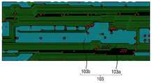
도 4는 도 3의 메인기판의 디스플레이면 반대면의 일부확대 평면도이다.FIG. 4 is a partially enlarged plan view of a surface opposite to a display surface of the main board of FIG. 3.
전술한 바와 같이, 상기 메인기판(100)의 상기 디스플레이면 반대면(102)에 형성되어, 상기 구동칩의 리드(121)와 결합하는 동박패턴(103)을 더 포함하고, 상기 동박패턴 중 상기 구동칩의 접지 리드(121b)와 결합하는 접지를 위한 접지용 동박패드(103b)는 폭이 신호를 전달하기 위한 신호용 동박패턴(103a) 보다 넓게 형성된다. 즉, 구동칩(120)은 반도체칩과 메인기판의 전기적 신호를 전달할 수 있도록 다수의 리드(121)가 형성되며, 상기 리드(121)는 신호를 전달을 위한 리드(121a)와 접지를 위한 접지 리드(121b)를 포함한다.As described above, a
이와 같이 접지리드(121a)와 결합되는 접지용 동박패드(103b)가 다른 신호 전달을 위한 신호용 동박패드(103a) 보다 넓게 형성되어, 구동칩에서 발생되어 리드를 통해서 전달된 열을 가능한 후방으로 잘 배출할 수 있도록 한다.In this way, the ground
특히, 도 5에 도시된 바와 같이, 상기 접지용 동박패턴(103b)은 상기 신호용 동박 패턴(103a)으로 둘러쌓인 영역 전체에 걸쳐서 형성된 것이 바람직하다. 둘러쌓인 영역 전체에 걸쳐서 형성된 다는 것은 신호용 동박 패턴(103a)으로 돌러쌓인 영역에서 최대한 접지용 동박패턴(103b)을 형성하는 것으로서, 접지용 동박패턴(103b)을 신호용 동박 패턴(103a)에 간섭을 일으키지 않는 한 가능한 많은 영역에 형성하는 것을 의미한다.In particular, as shown in FIG. 5, the ground
상기 전면 커버(600)는 엘이디 소자(110)만 드러나도록 개구(601)가 형성되어, 구동칩(120)과 같은 부품이 외부로 드러나, 미관을 해치거나, 손상되는 것을 방지한다.The
도 6은 도 1의 전면 커버와 메인보드가 결합된 상태의 측단면도이다.6 is a side cross-sectional view of the front cover and the main board of FIG.
상기 전면 커버(600)와 상기 디스플레이면(101) 사이에 간극을 유지하기 위한 스페이서(421)를 더 포함하는 것이 바람직하다. 즉, 메인기판(100)은 후방커버의 기판 지지부(422, 스크류와 결합할 수 있는 보스 혹은 지지턱 등으로 구현될 수있다.)에 의해 지지되고, 전면커버(600)는 메인기판(100)에 별도의 스페이서(421)에 의해 간격을 유지하도록 설치된다.It is preferable to further include a
도 7은 도 6의 변형예를 도시한 측단면도이다.FIG. 7 is a side sectional view showing a modification of FIG. 6. FIG.
도 6에서는 도 5와 달리, 전면 커버(600) 및 메인기판(100) 모두 후방커버(400)에 의해 지지된다. 즉, 후방커버의 기판 지지부(422)에 의해 메인기판(100)이 지지되며, 후방커버의 전면커버 지지부(423)에 의해 전면커버(600)가 지지된다. 다만, 전면커버 지지부(423)의 길이가 기판 지지부(422) 보다 높이가 높게 형성됨으로써, 전면커버와 메인기판(100)의 간격이 유지된다. 따라서, 도 6에서는 전면커버 지지부(423)가 스페이서에 해당한다.In FIG. 6, unlike the FIG. 5, both the
상기와 같이, 스페이서를 구비함으로써, 메인기판에서 발생되는 열이 보다 효과적으로 전면으로 방출될 수 있도록 한다.As described above, by providing the spacer, the heat generated from the main substrate can be more effectively discharged to the front surface.
커넥터(300)는 제어신호 및 전원을 공급받을 수 있는 케이블과 연결되는 단자이다. 커넥터(300)는 방수용 커넥터가 사용되는 것이 바람직하다. 방수용 커넥터는 일반 시중에 많이 알려져 있으므로, 구체적인 내용은 기재하지 않는다. 방수용 커넥터가 사용됨으로써, 개별 디스플레이 모듈별로 방수가 가능하여, 디스플레이 장치 전체의 후방을 방수하기 위한 캐비넷과 같은 장치가 불필요하다는 장점이 있다.The connector 300 is a terminal connected to a cable capable of receiving a control signal and power. The connector 300 is preferably a waterproof connector. Since waterproof connectors are widely known on the market, specific details are not described. By using the waterproof connector, it is possible to waterproof each individual display module, there is an advantage that a device such as a cabinet for waterproofing the rear of the entire display device is unnecessary.
전원부(200)는 커넥터(300)로 부터 전달된 전원을 적절한 전압으로 변압하여 메인기판(100)에 공급하는 역할을 한다. 전원부(200)가 변압을 하는 과정에서 열이 발생하며, 이와같은 열을 효과적으로 방출하기 위한 구조가 요청된다.The power supply unit 200 serves to supply power to the
후방 커버(400)는 전술한 메인기판(100), 전면커버(600), 전원부(200) 및 커넥터(300)를 고정하는 역할을 하며, 커넥터(300)에 케이블이 외부에서 연결될 수 있도록 커넥터 연결공(420)이 관통되어 형성되며, 전원부(200)를 감싸는 위치에 후방방열부(410)가 개방되어 형성된다. 전술한 바와 같이, 후방방열부(410)에는 후방 방열판(500)이 결합된다. 후방 방열판(500)은 후방방열부(410)를 통해서 전달되는 열을 보다 효과적으로 방출하기 위해 금속으로 다수의 핀을 구비하도록 형성된다.The rear cover 400 serves to fix the
따라서, 전원부 및 메인기판(100)의 후방에서 발생되는 열을 효과적으로 방출할 수 있다.Therefore, it is possible to effectively dissipate heat generated from the back of the power supply unit and the
이상에서는 본 발명의 바람직한 실시예를 예시적으로 설명하였으나, 본 발명의 범위는 이와 같은 특정 실시예에만 한정되는 것은 아니며, 특허청구범위에 기재된 범주 내에서 적절하게 변경 가능한 것이다.While the present invention has been particularly shown and described with reference to exemplary embodiments thereof, it is to be understood that the invention is not limited to the disclosed embodiments, but, on the contrary, is intended to cover various modifications and equivalent arrangements included within the spirit and scope of the invention.
**도면의 주요부분에 대한 부호의 설명**
101: 디스플레이면110: 엘이디 소자
100: 메인기판120: 엘이디 구동칩
130: 방수용 몰드103: 동박패턴
121b: 구동칩의 접지 리드103b: 접지용 동박패턴
600: 전면 커버421, 423: 스페이서
200: 전원부300: 커넥터
410: 후방방열부400: 후방커버
500: 후방 방열판DESCRIPTION OF REFERENCE NUMERALS
101: display surface 110: LED element
100: main board 120: LED driving chip
130: waterproof mold 103: copper foil pattern
121b: Ground lead of driving
600:
200: power supply unit 300: connector
410: rear radiator 400: rear cover
500: rear heat sink
Claims (8)
Translated fromKorean표면이 상기 디스플레이면에 드러나도록 상기 메인기판에 설치된 엘이디 구동칩;
상기 메인기판의 상기 디스플레이면에 코팅되며, 상기 엘이디 소자의 표면과, 상기 엘이디 구동칩의 표면이 드러나는 두께로 형성된 방수용 몰드;
상기 메인기판의 상기 디스플레이면 반대면에 결합되는 전원부 및 커넥터;
상기 전원부 및 상기 커넥터를 감싸며 상기 메인기판과 결합하며, 상기 전원부를 감싸는 일부인 후방방열부가 개방된 후방커버; 및
상기 후방방열부를 밀폐하도록 상기 후방커버에 결합되는 후방 방열판;
을 포함하는 것을 특징으로 하는 엘이디 디스플레이 장치.
A main board on which a plurality of LED elements are installed on a display surface;
An LED driving chip mounted on the main substrate so that a surface thereof is exposed on the display surface;
A waterproof mold coated on the display surface of the main substrate and formed to have a thickness at which the surface of the LED element and the surface of the LED driving chip are exposed;
A power supply unit and a connector coupled to an opposite surface of the display surface of the main board;
A rear cover surrounding the power supply unit and the connector, coupled to the main board, and a rear heat dissipation unit which is a part surrounding the power supply unit; And
A rear heat sink coupled to the rear cover to seal the rear heat sink;
LED display device comprising a.
표면이 상기 디스플레이면에 드러나도록 상기 메인기판에 설치된 엘이디 구동칩;
상기 메인기판의 상기 디스플레이면에 코팅되며, 상기 엘이디 소자의 표면과, 상기 엘이디 구동칩의 표면이 드러나는 두께로 형성된 방수용 몰드;
상기 메인기판의 상기 디스플레이면 반대면에 형성되어, 신호를 전달하는 신호용 동박패턴; 및
상기 메인기판의 상기 디스플레이면 반대면에 형성되며, 상기 구동칩의 접지 리드와 결합하는 접지용 동박패턴;
을 포함하고,
상기 접지용 동박 패턴은 폭이 상기 신호용 동박패턴 보다 넓게 형성된 것을 특징으로 하는 엘이디 디스플레이 장치.
A main board on which a plurality of LED elements are installed on a display surface;
An LED driving chip mounted on the main substrate so that a surface thereof is exposed on the display surface;
A waterproof mold coated on the display surface of the main substrate and formed to have a thickness at which the surface of the LED element and the surface of the LED driving chip are exposed;
A copper foil pattern for a signal formed on an opposite surface of the main substrate to transmit a signal; And
A ground copper foil pattern formed on an opposite side of the display surface of the main substrate and coupled to a ground lead of the driving chip;
/ RTI >
And the ground copper foil pattern is wider than the signal copper foil pattern.
상기 접지용 동박패턴은 상기 신호용 동박 패턴으로 둘러쌓인 영역 전체에 걸쳐서 형성된 것을 특징으로 하는 엘이디 디스플레이 장치.
The method of claim 2,
The ground copper foil pattern is an LED display device, characterized in that formed over the entire area surrounded by the signal copper foil pattern.
표면이 상기 디스플레이면에 드러나도록 상기 메인기판에 설치된 엘이디 구동칩;
상기 메인기판의 상기 디스플레이면에 코팅되며, 상기 엘이디 소자의 표면과, 상기 엘이디 구동칩의 표면이 드러나는 두께로 형성된 방수용 몰드; 및
상기 디스플레이면에 결합되며, 개별 상기 엘이디 소자가 드러나도록 격자 형상으로 형성된 전면 커버;
를 더 포함하는 것을 특징으로 하는 엘이디 디스플레이 장치.
A main board on which a plurality of LED elements are installed on a display surface;
An LED driving chip mounted on the main substrate so that a surface thereof is exposed on the display surface;
A waterproof mold coated on the display surface of the main substrate and formed to have a thickness at which the surface of the LED element and the surface of the LED driving chip are exposed; And
A front cover coupled to the display surface and formed in a lattice shape so that the individual LED elements are exposed;
LED display device further comprises.
상기 전면 커버와 상기 디스플레이면 사이에 간극을 유지하기 위한 스페이서;
를 더 포함하는 것을 특징으로 하는 엘이디 디스플레이 장치.
The method of claim 4, wherein
A spacer for maintaining a gap between the front cover and the display surface;
LED display device further comprises.
상기 메인기판의 상기 디스플레이면 반대면에 형성되어, 신호를 전달하는 신호용 동박패턴; 및
상기 메인기판의 상기 디스플레이면 반대면에 형성되며, 상기 구동칩의 접지 리드와 결합하는 접지용 동박패턴;
을 더 포함하고,
상기 접지용 동박 패턴은 폭이 상기 신호용 동박패턴 보다 넓게 형성된 것을 특징으로 하는 엘이디 디스플레이 장치.
The method of claim 5, wherein
A copper foil pattern for a signal formed on an opposite surface of the main substrate to transmit a signal; And
A ground copper foil pattern formed on an opposite side of the display surface of the main substrate and coupled to a ground lead of the driving chip;
Further comprising:
And the ground copper foil pattern is wider than the signal copper foil pattern.
상기 메인기판의 상기 디스플레이면 반대면에 결합되는 전원부 및 커넥터;
상기 전원부 및 상기 커넥터를 감싸며 상기 메인기판과 결합하며, 상기 전원부를 감싸는 일부인 후방방열부가 개방된 후방커버; 및
상기 후방방열부를 밀폐하도록 상기 후방커버에 결합되는 후방 방열판;
을 더 포함하는 것을 특징으로 하는 엘이디 디스플레이 장치.
7. The method according to any one of claims 2 to 6,
A power supply unit and a connector coupled to an opposite surface of the display surface of the main board;
A rear cover surrounding the power supply unit and the connector, coupled to the main board, and a rear heat dissipation unit which is a part surrounding the power supply unit; And
A rear heat sink coupled to the rear cover to seal the rear heat sink;
LED display device further comprises.
상기 커넥터는, 방수형 커넥터인 것을 특징으로 하는 엘이디 디스플레이 장치.
The method of claim 7, wherein
The connector is an LED display device, characterized in that the waterproof connector.
Priority Applications (1)
| Application Number | Priority Date | Filing Date | Title |
|---|---|---|---|
| KR1020100084618AKR101249763B1 (en) | 2010-08-31 | 2010-08-31 | LED Display Apparatus |
Applications Claiming Priority (1)
| Application Number | Priority Date | Filing Date | Title |
|---|---|---|---|
| KR1020100084618AKR101249763B1 (en) | 2010-08-31 | 2010-08-31 | LED Display Apparatus |
Publications (2)
| Publication Number | Publication Date |
|---|---|
| KR20120020780A KR20120020780A (en) | 2012-03-08 |
| KR101249763B1true KR101249763B1 (en) | 2013-04-03 |
Family
ID=46129316
Family Applications (1)
| Application Number | Title | Priority Date | Filing Date |
|---|---|---|---|
| KR1020100084618AExpired - Fee RelatedKR101249763B1 (en) | 2010-08-31 | 2010-08-31 | LED Display Apparatus |
Country Status (1)
| Country | Link |
|---|---|
| KR (1) | KR101249763B1 (en) |
Cited By (2)
| Publication number | Priority date | Publication date | Assignee | Title |
|---|---|---|---|---|
| US10741107B2 (en) | 2013-12-31 | 2020-08-11 | Ultravision Technologies, Llc | Modular display panel |
| US10891881B2 (en) | 2012-07-30 | 2021-01-12 | Ultravision Technologies, Llc | Lighting assembly with LEDs and optical elements |
Citations (2)
| Publication number | Priority date | Publication date | Assignee | Title |
|---|---|---|---|---|
| KR20070096711A (en)* | 2006-03-27 | 2007-10-02 | 엘지이노텍 주식회사 | Light emitting diode lighting device and manufacturing method thereof |
| KR100877294B1 (en) | 2008-04-10 | 2009-01-07 | 주식회사 포트론 | LED scoreboard |
- 2010
- 2010-08-31KRKR1020100084618Apatent/KR101249763B1/ennot_activeExpired - Fee Related
Patent Citations (2)
| Publication number | Priority date | Publication date | Assignee | Title |
|---|---|---|---|---|
| KR20070096711A (en)* | 2006-03-27 | 2007-10-02 | 엘지이노텍 주식회사 | Light emitting diode lighting device and manufacturing method thereof |
| KR100877294B1 (en) | 2008-04-10 | 2009-01-07 | 주식회사 포트론 | LED scoreboard |
Cited By (2)
| Publication number | Priority date | Publication date | Assignee | Title |
|---|---|---|---|---|
| US10891881B2 (en) | 2012-07-30 | 2021-01-12 | Ultravision Technologies, Llc | Lighting assembly with LEDs and optical elements |
| US10741107B2 (en) | 2013-12-31 | 2020-08-11 | Ultravision Technologies, Llc | Modular display panel |
Also Published As
| Publication number | Publication date |
|---|---|
| KR20120020780A (en) | 2012-03-08 |
Similar Documents
| Publication | Publication Date | Title |
|---|---|---|
| AU2006230909B2 (en) | Light emitting array apparatus and method of manufacture | |
| US8598616B2 (en) | Light emitting device and light unit using the same | |
| US8075152B2 (en) | Hermetic light-emitting device | |
| CN101482252B (en) | Convection cooling type LED illumination device | |
| JP2003303504A (en) | Illumination apparatus using light emitting diode | |
| US9128222B1 (en) | LED lighting apparatus | |
| GB2424124A (en) | LED mounting assembly | |
| JP4969332B2 (en) | Substrate and lighting device | |
| JP2004055229A (en) | Led lighting system and lighting equipment | |
| KR20080057564A (en) | Outdoor LED Board Using Chip LED Module | |
| KR20170005664A (en) | Lighting device module | |
| KR101956765B1 (en) | Flexible LED display | |
| KR101249763B1 (en) | LED Display Apparatus | |
| WO2005103564A1 (en) | Led light source module packaged with metal | |
| CN107710062A (en) | Structure for connecting printed circuit boards and display device having said structure | |
| KR20080067893A (en) | Waterproof LED Module | |
| JP2007258136A (en) | Light source and lighting system | |
| JPH0850458A (en) | Light emitting display device | |
| JP2007109945A (en) | Light source | |
| KR20020069818A (en) | An ultra-slim type led module and an electric signboard using the same | |
| US20140347855A1 (en) | Led luminaire | |
| TWI874158B (en) | Light fixture with moisture resistance | |
| US11956891B2 (en) | Electronic module | |
| KR20120060991A (en) | Light Emitting Device Module | |
| KR101098951B1 (en) | Light emitting device |
Legal Events
| Date | Code | Title | Description |
|---|---|---|---|
| A201 | Request for examination | ||
| PA0109 | Patent application | St.27 status event code:A-0-1-A10-A12-nap-PA0109 | |
| PA0201 | Request for examination | St.27 status event code:A-1-2-D10-D11-exm-PA0201 | |
| D13-X000 | Search requested | St.27 status event code:A-1-2-D10-D13-srh-X000 | |
| D14-X000 | Search report completed | St.27 status event code:A-1-2-D10-D14-srh-X000 | |
| PE0902 | Notice of grounds for rejection | St.27 status event code:A-1-2-D10-D21-exm-PE0902 | |
| P11-X000 | Amendment of application requested | St.27 status event code:A-2-2-P10-P11-nap-X000 | |
| P13-X000 | Application amended | St.27 status event code:A-2-2-P10-P13-nap-X000 | |
| PG1501 | Laying open of application | St.27 status event code:A-1-1-Q10-Q12-nap-PG1501 | |
| E701 | Decision to grant or registration of patent right | ||
| PE0701 | Decision of registration | St.27 status event code:A-1-2-D10-D22-exm-PE0701 | |
| GRNT | Written decision to grant | ||
| PR0701 | Registration of establishment | St.27 status event code:A-2-4-F10-F11-exm-PR0701 | |
| PR1002 | Payment of registration fee | St.27 status event code:A-2-2-U10-U11-oth-PR1002 Fee payment year number:1 | |
| PG1601 | Publication of registration | St.27 status event code:A-4-4-Q10-Q13-nap-PG1601 | |
| R18-X000 | Changes to party contact information recorded | St.27 status event code:A-5-5-R10-R18-oth-X000 | |
| LAPS | Lapse due to unpaid annual fee | ||
| PC1903 | Unpaid annual fee | St.27 status event code:A-4-4-U10-U13-oth-PC1903 Not in force date:20160328 Payment event data comment text:Termination Category : DEFAULT_OF_REGISTRATION_FEE | |
| P22-X000 | Classification modified | St.27 status event code:A-4-4-P10-P22-nap-X000 | |
| PC1903 | Unpaid annual fee | St.27 status event code:N-4-6-H10-H13-oth-PC1903 Ip right cessation event data comment text:Termination Category : DEFAULT_OF_REGISTRATION_FEE Not in force date:20160328 | |
| P22-X000 | Classification modified | St.27 status event code:A-4-4-P10-P22-nap-X000 | |
| P22-X000 | Classification modified | St.27 status event code:A-4-4-P10-P22-nap-X000 |