KR101248910B1 - Switching mode power supply and image forming device having the same and method of driving thereof - Google Patents
Switching mode power supply and image forming device having the same and method of driving thereofDownload PDFInfo
- Publication number
- KR101248910B1 KR101248910B1KR1020060073646AKR20060073646AKR101248910B1KR 101248910 B1KR101248910 B1KR 101248910B1KR 1020060073646 AKR1020060073646 AKR 1020060073646AKR 20060073646 AKR20060073646 AKR 20060073646AKR 101248910 B1KR101248910 B1KR 101248910B1
- Authority
- KR
- South Korea
- Prior art keywords
- switching signal
- unit
- potential
- switching
- frequency
- Prior art date
- Legal status (The legal status is an assumption and is not a legal conclusion. Google has not performed a legal analysis and makes no representation as to the accuracy of the status listed.)
- Expired - Fee Related
Links
Images


Classifications
- H—ELECTRICITY
- H02—GENERATION; CONVERSION OR DISTRIBUTION OF ELECTRIC POWER
- H02M—APPARATUS FOR CONVERSION BETWEEN AC AND AC, BETWEEN AC AND DC, OR BETWEEN DC AND DC, AND FOR USE WITH MAINS OR SIMILAR POWER SUPPLY SYSTEMS; CONVERSION OF DC OR AC INPUT POWER INTO SURGE OUTPUT POWER; CONTROL OR REGULATION THEREOF
- H02M3/00—Conversion of DC power input into DC power output
- H02M3/22—Conversion of DC power input into DC power output with intermediate conversion into AC
- H02M3/24—Conversion of DC power input into DC power output with intermediate conversion into AC by static converters
- H02M3/28—Conversion of DC power input into DC power output with intermediate conversion into AC by static converters using discharge tubes with control electrode or semiconductor devices with control electrode to produce the intermediate AC
- H02M3/325—Conversion of DC power input into DC power output with intermediate conversion into AC by static converters using discharge tubes with control electrode or semiconductor devices with control electrode to produce the intermediate AC using devices of a triode or a transistor type requiring continuous application of a control signal
- H02M3/335—Conversion of DC power input into DC power output with intermediate conversion into AC by static converters using discharge tubes with control electrode or semiconductor devices with control electrode to produce the intermediate AC using devices of a triode or a transistor type requiring continuous application of a control signal using semiconductor devices only
- H02M3/33507—Conversion of DC power input into DC power output with intermediate conversion into AC by static converters using discharge tubes with control electrode or semiconductor devices with control electrode to produce the intermediate AC using devices of a triode or a transistor type requiring continuous application of a control signal using semiconductor devices only with automatic control of the output voltage or current, e.g. flyback converters
- G—PHYSICS
- G03—PHOTOGRAPHY; CINEMATOGRAPHY; ANALOGOUS TECHNIQUES USING WAVES OTHER THAN OPTICAL WAVES; ELECTROGRAPHY; HOLOGRAPHY
- G03G—ELECTROGRAPHY; ELECTROPHOTOGRAPHY; MAGNETOGRAPHY
- G03G15/00—Apparatus for electrographic processes using a charge pattern
- H—ELECTRICITY
- H02—GENERATION; CONVERSION OR DISTRIBUTION OF ELECTRIC POWER
- H02M—APPARATUS FOR CONVERSION BETWEEN AC AND AC, BETWEEN AC AND DC, OR BETWEEN DC AND DC, AND FOR USE WITH MAINS OR SIMILAR POWER SUPPLY SYSTEMS; CONVERSION OF DC OR AC INPUT POWER INTO SURGE OUTPUT POWER; CONTROL OR REGULATION THEREOF
- H02M1/00—Details of apparatus for conversion
- H02M1/0003—Details of control, feedback or regulation circuits
- H02M1/0032—Control circuits allowing low power mode operation, e.g. in standby mode
- H—ELECTRICITY
- H02—GENERATION; CONVERSION OR DISTRIBUTION OF ELECTRIC POWER
- H02M—APPARATUS FOR CONVERSION BETWEEN AC AND AC, BETWEEN AC AND DC, OR BETWEEN DC AND DC, AND FOR USE WITH MAINS OR SIMILAR POWER SUPPLY SYSTEMS; CONVERSION OF DC OR AC INPUT POWER INTO SURGE OUTPUT POWER; CONTROL OR REGULATION THEREOF
- H02M1/00—Details of apparatus for conversion
- H02M1/44—Circuits or arrangements for compensating for electromagnetic interference in converters or inverters
- Y—GENERAL TAGGING OF NEW TECHNOLOGICAL DEVELOPMENTS; GENERAL TAGGING OF CROSS-SECTIONAL TECHNOLOGIES SPANNING OVER SEVERAL SECTIONS OF THE IPC; TECHNICAL SUBJECTS COVERED BY FORMER USPC CROSS-REFERENCE ART COLLECTIONS [XRACs] AND DIGESTS
- Y02—TECHNOLOGIES OR APPLICATIONS FOR MITIGATION OR ADAPTATION AGAINST CLIMATE CHANGE
- Y02B—CLIMATE CHANGE MITIGATION TECHNOLOGIES RELATED TO BUILDINGS, e.g. HOUSING, HOUSE APPLIANCES OR RELATED END-USER APPLICATIONS
- Y02B70/00—Technologies for an efficient end-user side electric power management and consumption
- Y02B70/10—Technologies improving the efficiency by using switched-mode power supplies [SMPS], i.e. efficient power electronics conversion e.g. power factor correction or reduction of losses in power supplies or efficient standby modes
Landscapes
- Engineering & Computer Science (AREA)
- Power Engineering (AREA)
- Physics & Mathematics (AREA)
- General Physics & Mathematics (AREA)
- Dc-Dc Converters (AREA)
Abstract
Translated fromKoreanDescription
Translated fromKorean도 1은 본 발명의 일 실시예에 의한 화상형성장치를 설명하기 위해 도시한 블록도이다.1 is a block diagram illustrating an image forming apparatus according to an embodiment of the present invention.
도 2는 본 발명의 일 실시예에 의한 스위칭 모드 전원공급장치를 설명하기 위해 도시한 블록도이다.2 is a block diagram illustrating a switching mode power supply apparatus according to an embodiment of the present invention.
도 3은 본 발명의 일 실시예에 의한 스위칭 모드 전원공급장치의 구체적인 실시예를 도시한 회로도이다.3 is a circuit diagram showing a specific embodiment of a switching mode power supply according to an embodiment of the present invention.
도 4는 본 발명의 일 실시예에 의한 스위칭 모드 전원공급장치의 구체적인 실시예를 도시한 다른 회로도이다.Figure 4 is another circuit diagram showing a specific embodiment of a switched mode power supply according to an embodiment of the present invention.
도 5는 본 발명의 일 실시예에 의한 스위칭 모드 전원공급장치의 구동을 설명하기 위한 파형도이다.5 is a waveform diagram illustrating the driving of a switching mode power supply apparatus according to an embodiment of the present invention.
도 6은 비교예에 의한 준 공진 제어 방식을 이용하는 스위칭 모드 전원공급장치의 일부분을 도시한 회로도이다.6 is a circuit diagram illustrating a part of a switching mode power supply using a quasi-resonant control method according to a comparative example.
도 7은 도 6에 도시된 제어부에 인가되는 파형의 일례를 도시한 도면이다.FIG. 7 is a diagram illustrating an example of waveforms applied to the controller illustrated in FIG. 6.
도 8은 도 7에 도시된 파형이 도 6에 도시된 제어부에 인가됨에 따른 SMPS의 동작을 설명하기 위한 도면이다.FIG. 8 is a diagram for describing an operation of the SMPS as the waveform shown in FIG. 7 is applied to the controller shown in FIG. 6.
*도면의 주요 부분에 대한 부호의 설명*Description of the Related Art [0002]
100 : 화상형성장치200 : 전원 공급부100: image forming apparatus 200: power supply unit
220 : 전원 변환부240 : 공진 회로부220: power conversion unit 240: resonant circuit unit
242 : 임피던스 감지부244 : 시비율 변환부242: impedance detection unit 244: ratio ratio conversion unit
260 : 신호 제어부280 : 과전류 검출부260: signal controller 280: overcurrent detector
300 : 인쇄 제어부400 ; 인쇄 엔진부300:
본 발명은 스위칭 모드 전원공급장치, 이를 구비한 화상형성장치 및 이의 구동 방법에 관한 것으로서, 보다 구체적으로는 부하단의 임피던스 변동에 따른 전자파 장애 현상을 방지하고, 전력 소모의 절감을 도모한 스위칭 모드 전원공급장치, 이를 구비한 화상형성장치 및 이의 구동 방법에 관한 것이다.BACKGROUND OF THE INVENTION 1. Field of the Invention The present invention relates to a switching mode power supply, an image forming apparatus having the same, and a driving method thereof. More particularly, the present invention relates to a switching mode that prevents electromagnetic interference due to impedance variation of a load stage and reduces power consumption. A power supply apparatus, an image forming apparatus having the same, and a driving method thereof are provided.
화상형성장치는 입력되는 화상 데이터에 대응하는 이미지를 인쇄 용지가 같은 기록 매체에 인쇄 처리하는 장치를 의미한다. 이러한 화상형성장치의 예로는 프린터,복사기, 팩시밀리 및 이들의 기능을 하나로 통합한 복합기 등을 들 수 있다.The image forming apparatus means an apparatus which prints an image corresponding to input image data onto a recording medium having the same print sheet. Examples of such an image forming apparatus include a printer, a copying machine, a facsimile, and a multifunction printer incorporating these functions into one.
이러한 화상형성장치는 각각의 인쇄 처리를 수행하기 위해 외부로부터 인가되는 교류 전원을 직류 전원으로 변환하여, 화상형성장치의 각 부 예를 들어, 인쇄 동작을 제어하는 마이크로 콘트롤러 등을 구비한 인쇄 제어부 및 인쇄 용지와 같은 기록 매체를 적재하고, 이송하며, 기록 용지 상에 소정 화상을 형성하며, 화상이 형성된 기록 용지를 배출하는 인쇄 엔진부로 제공하는 전원공급장치를 필요로 한다.Such an image forming apparatus includes a print control unit having a microcontroller for controlling each printing part of the image forming apparatus, for example, by converting an AC power applied from the outside into a DC power source to perform each print process; There is a need for a power supply that loads and transports a recording medium such as printing paper, forms a predetermined image on the recording paper, and provides the power supply to the print engine unit for discharging the recording paper on which the image is formed.
일반적으로, 이러한 전원공급장치는 상용 교류를 정류 및 평활하여 얻어진 직류 전류를 소정 고주파 예를 들어, 100kHz 정도의 고주파로 스위칭하여 변압기에 의해 원하는 전압으로 고효율로 변환되도록 하는 스위칭 모드 전원공급장치(Switching Mode Power Supply; 이하 SMPS)가 널리 사용되고 있다.In general, such a power supply is a switching mode power supply for switching a direct current obtained by rectifying and smoothing commercial alternating current to a predetermined high frequency, for example, 100 kHz, so that the transformer is converted into a desired voltage with high efficiency. Mode Power Supply (SMPS) is widely used.
이러한 SMPS의 출력 전압의 제어 방식으로는, 출력 전압의 변화에 따라 스위칭 펄스의 시비율(duty ratio)을 제어하는 펄스 폭 변조(Pulse Width Modulation; 이하, PWM) 제어 방식, 스위칭 펄스의 주파수를 제어하는 주파수 제어 방식 및 스위칭 펄스의 위상을 제어하는 위상 제어 방식 등이 있다.As such a method of controlling the output voltage of the SMPS, a pulse width modulation (PWM) control method for controlling the duty ratio of the switching pulse according to the change of the output voltage, and the frequency of the switching pulse are controlled. And a phase control method for controlling the phase of the switching pulse.
최근 들어, 화상형성장치는 그 기능의 다양화 및 복잡화되는 추세에 있으며, 이와 더불어 저 소비 전력화를 도모하고 있는 추세에 있다. 따라서, SMPS 또한 그 차체의 소비 전력의 절감을 도모하기 위해 다양한 방법이 사용되고 있다.In recent years, the image forming apparatus has been diversified and complicated in its function, and at the same time, it has become a trend to lower the power consumption. Therefore, SMPS is also used in various ways to reduce the power consumption of the vehicle body.
이러한 소비 전력의 절감을 도모하는 한 방법으로써, SMPS에 준 공진(quasi resonant) 제어 방식을 적용하는 방법이 사용되고 있다.As one method of reducing such power consumption, a method of applying a quasi resonant control method to the SMPS has been used.
이러한 준 공진 제어 방식을 간략히 설명하면 다음과 같다.Briefly, the quasi-resonance control method is as follows.
도 6은 비교예에 의한 준 공진 제어 방식을 이용하는 SMPS의 일부분을 도시한 회로도이고, 도 7은 도 6에 도시된 제어부에 인가되는 파형의 일례를 도시한 도면이며, 도 8은 도 7에 도시된 파형이 도 6에 도시된 제어부에 인가됨에 따른 SMPS 의 동작을 설명하기 위한 도면이다.FIG. 6 is a circuit diagram illustrating a part of an SMPS using a quasi-resonant control method according to a comparative example. FIG. 7 is a diagram illustrating an example of waveforms applied to the controller illustrated in FIG. 6, and FIG. 8 is illustrated in FIG. 7. FIG. 6 is a view for explaining the operation of the SMPS according to the applied waveform to the control unit shown in FIG.
일반적으로, 준 공진 제어 방식은 도 6에 도시된 모스 트랜지스터(M_TR)가 턴-온(turn-on) 상태에서 턴-오프(turn-off) 상태로 변화할 때, 변동되는 모스 트랜지스터(M_TR) 양단의 전위가 최소 지점일 때 모스 트랜지스터(M_TR)가 도통을 시작하여 새로운 사이클을 다시 시작하도록 트리거(trigger) 하는 제어 방식이다. 이에 따라, 모스 트랜지스터(M_TR)의 소비 전력을 절감이 가능하여 SMPS의 소비 전력 절감을 도모할 수 있다.In general, the quasi-resonant control method is a MOS transistor (M_TR) that is changed when the MOS transistor (M_TR) shown in Figure 6 changes from the turn-on (turn-on) state to turn-off (turn-off) state When the potential at both ends is the minimum point, the MOS transistor M_TR triggers the conduction and triggers a new cycle again. Accordingly, power consumption of the MOS transistor M_TR can be reduced, and power consumption of the SMPS can be reduced.
도 6 내지 도 8을 참조하면, 제어부(IC)는 전원 전압(VCC)이 인가됨에 따라 구동하여 모스 트랜지스터(M_TR)의 스위칭 동작을 제어하는 소정 주파수를 갖는 스위칭 신호를 출력한다. 이에 따라, 변압기의 1차측 권선(L11)에는 외부 전원이 정류 및 평활된 직류 전원(DC_IN)이 인가되고, 스위칭 신호에 의해 1차측 권선(L11)에 인가되는 직류 전원(DC_IN)은 소정 펄스 형상의 직류 전원이 인가된다.6 to 8, the controller IC drives when the power supply voltage VCC is applied to output a switching signal having a predetermined frequency for controlling the switching operation of the MOS transistor M_TR. Accordingly, the DC power supply DC_IN rectified and smoothed with the external power is applied to the primary winding L11 of the transformer, and the DC power supply DC_IN applied to the primary winding L11 by the switching signal has a predetermined pulse shape. DC power supply is applied.
이는 변압기의 2차측 권선(L12)에 스위칭 신호의 주파수와 실질적으로 동일한 주파수를 갖는 원시 스위칭 신호를 생성하고, 생성된 원시 스위칭 신호는 2차측 권선(L12)의 인덕턴스와 커패시터(C1)의 커패시턴스에 의해 형성된 고정된 공진 주파수에 의해 공진되며, 선택된 주파수 대역대의 스위칭 신호는 P3 지점에서 검출하면 도 8에 도시된 바와 같은 파형으로 제어부(IC)에 인가된다.This produces a raw switching signal having a frequency substantially the same as the frequency of the switching signal in the secondary winding L12 of the transformer, and the generated raw switching signal is applied to the inductance of the secondary winding L12 and the capacitance of the capacitor C1. Resonance is performed by a fixed resonance frequency formed by the switching signal, and the switching signal of the selected frequency band is applied to the controller IC in a waveform as shown in FIG. 8 when it is detected at the point P3.
이에 따라, 제어부(IC)는 인가되는 주파수 대역대의 스위칭 신호가 기준 전위 예를 들어, 0 전위과 동일한 전위를 갖는 위상을 검출하고, 스위칭 신호가 0 전위 이하로 제공되는 시간이 소정 시간, 예를 들어 8us 정도가 경과하면, 도 8에 도 시된 바와 같이 모스 트랜지스터(M_TR)로 스위칭 신호를 출력함으로써, 준 공진 제어 방식을 이용하여 SMPS를 구동한다.Accordingly, the controller IC detects a phase in which the switching signal of the applied frequency band has a potential equal to the reference potential, for example, the zero potential, and the time for which the switching signal is provided below the zero potential is a predetermined time, for example, When about 8us has elapsed, as shown in FIG. 8, the switching signal is output to the MOS transistor M_TR, thereby driving the SMPS using a quasi-resonant control method.
그러나, 이와 같은 구조와 방식을 이용하여 SMPS를 구성하는 경우, 인덕턴스 및 커패시터 값에 의해 코어(core)가 리셋(reset) 될 때까지 공진을 계속하게 되고, 공진 기간 중 도 7에 도시된 바와 같이 0 전위가 검출된 상태에서 일정 시간 이상이 0 전위 이하로 형성될 때마다 제어부(IC)가 스위칭 신호를 출력하기 때문에 SMPS의 출력단에 경 부하가 인가되었을 경우, 유도 전류가 낮게 되어 스위칭 주파수가 증가하게 된다.However, in the case of configuring the SMPS using such a structure and method, the resonance is continued until the core is reset by the inductance and the capacitor value, and as shown in FIG. 7 during the resonance period. When the zero potential is detected, the controller IC outputs a switching signal each time a predetermined time is formed below the zero potential. Therefore, when a light load is applied to the output terminal of the SMPS, the induction current becomes low and the switching frequency increases. Done.
이는 저주파 신호의 경우 EMI를 측정 시 그 저주파 신호의 고조파 성분부터 감지되나 고주파 신호의 경우, 원 주파수 성분에서 감지되어 스위칭 주파수가 증가하게 됨에 따라 EMI 특성을 저하시키게 된다.The low frequency signal is detected from the harmonics of the low frequency signal when measuring the EMI, but the high frequency signal is detected from the original frequency component, thereby degrading the EMI characteristics as the switching frequency increases.
또한, 스위칭 신호의 출력 주기가 짧아짐에 따라 모스 트랜지스터(M_TR)의 턴-온 및 턴-오프 동작의 수행이 경 부하가 인가되었을 경우, 중 부하가 인가되었을 경우에 비해 증가하게 되어, 모스 트랜지스터(M_TR)에서의 소비 전력이 증가하게 되어 SMPS의 소비 전력이 증가하게 되는 문제점이 있다.In addition, as the output period of the switching signal is shortened, the turn-on and turn-off operations of the MOS transistor M_TR are increased when a light load is applied, compared to when a heavy load is applied, and thus the MOS transistor ( There is a problem that the power consumption of M_TR is increased to increase the power consumption of the SMPS.
본 발명은 상기한 문제점을 해결하기 위해 안출한 것으로서, 본 발명의 목적은 부하단의 임피던스 변동에 따라 EMI 특성의 저하를 방지하고, 소모 전력의 절감을 도모한 스위칭 모드 전원공급장치를 제공하는데 있다.SUMMARY OF THE INVENTION The present invention has been made to solve the above problems, and an object of the present invention is to provide a switching mode power supply device which prevents degradation of EMI characteristics due to impedance variation of a load stage and reduces power consumption. .
본 발명의 다른 목적은 상기 스위칭 모드 전원공급장치를 구비한 화상형성장 치를 제공하는데 있다.Another object of the present invention is to provide an image forming apparatus having the switching mode power supply.
본 발명의 또 다른 목적은 상기 스위칭 모드 전원공급장치의 구동 방법을 제공하는데 있다.Still another object of the present invention is to provide a method of driving the switched mode power supply.
상기한 본 발명의 목적을 달성하기 위하여, 본 발명의 일 실시예에 의한 스위칭 모드 전원공급장치는 전원 변환부, 공진 회로부 및 신호 제어부를 포함한다. 전원 변환부는 외부 전원을 스위칭 신호에 의해 내부 전원으로 변환하고, 상기 외부 전원에 기초하여 상기 스위칭 신호의 주파수를 가변하기 위한 원시 스위칭 신호를 출력한다. 상기 공진 회로부는 상기 내부 전원이 인가되는 부하단의 임피던스 변동에 따라 상기 원시 스위칭 신호의 시비율을 가변 공진 주파수를 이용하여 변경한다. 상기 신호 제어부는 상기 가변 공진 주파수에 의해 공진된 원시 스위칭 신호의 전위와 기 정의된 기준 전위를 비교하여, 소정 시간동안 상기 원시 스위칭 신호의 전위가 상기 기준 전위 이하의 전위로 형성되면, 상기 스위칭 신호의 주파수를 가변하여 출력한다.In order to achieve the above object of the present invention, the switching mode power supply apparatus according to an embodiment of the present invention includes a power conversion unit, a resonance circuit unit and a signal control unit. The power converter converts an external power source into an internal power source by a switching signal, and outputs a raw switching signal for varying the frequency of the switching signal based on the external power source. The resonant circuit unit changes the rate of application of the raw switching signal using a variable resonant frequency according to a change in impedance of a load terminal to which the internal power is applied. The signal controller compares the potential of the source switching signal resonated by the variable resonance frequency with a predefined reference potential, and when the potential of the source switching signal is formed to be equal to or lower than the reference potential for a predetermined time, the switching signal. Variable frequency is outputted.
상기 공진 회로부는, 상기 부하단의 임피던스 변동을 검출하여 시비율 제어 신호를 출력하는 임피던스 감지부 및 상기 시비율 제어 신호에 응답하여 상기 시비율을 변경하는 시비율 변환부를 포함한다.The resonant circuit unit may include an impedance detector configured to detect a change in impedance of the load terminal and output a ratio control signal, and a ratio ratio converter configured to change the ratio in response to the ratio control signal.
이때, 상기 시비율 변환부는, 상기 원시 스위칭 신호를 공진하기 위한 제1 충전부, 상기 제1 충전부와 병렬 연결되고, 상기 시비율 제어 신호에 응답하여 활성화되는 제1 스위칭부 및 상기 제1 스위칭부와 직렬 연결되고, 상기 제1 스위칭부 가 활성화되면 상기 제1 충전부와 함께 상기 공진 회로부의 가변 공진 주파수를 형성하는 제2 충전부를 포함할 수 있다.In this case, the ratio conversion unit, a first charging unit for resonating the source switching signal, the first switching unit and the first switching unit which is connected in parallel with the first charging unit and activated in response to the ratio control signal; When connected in series, and when the first switching unit is activated may include a second charging unit to form a variable resonant frequency of the resonant circuit unit with the first charging unit.
또한, 상기 임피던스 감지부는, 상기 부하단의 임피던스 변동에 따라 서로 다른 충전 전위로 형성되고, 상기 형성된 충전 전위를 상기 시비율 제어 신호로 출력하는 제3 충전부를 포함할 수 있다.The impedance sensing unit may include a third charging unit which is formed at different charging potentials according to the impedance variation of the load terminal and outputs the formed charging potential as the ratio control signal.
본 발명의 일 실시예에 의한 스위칭 모드 전원공급장치는 상기 전원 변환부로 과전류가 인가되면 상기 신호 제어부로 과전류 검출 신호를 출력하는 과전류 검출부를 더 포함할 수 있다.The switching mode power supply apparatus according to an embodiment of the present invention may further include an overcurrent detector for outputting an overcurrent detection signal to the signal controller when overcurrent is applied to the power converter.
여기서, 공진 회로부는 상기 과전류 검출부와 병렬 연결된다.Here, the resonant circuit part is connected in parallel with the overcurrent detector.
상기 전원 변환부는, 상기 스위칭 신호에 응답하여 활성화되어 상기 외부 전원의 전위를 변동시키는 제2 스위칭부를 더 포함할 수 있다.The power conversion unit may further include a second switching unit which is activated in response to the switching signal to change the potential of the external power source.
바람직하게는, 상기 전원 변환부는, 상기 외부 전원이 인가되는 1차측 권선, 상기 1차측 권선과 대향 배치되어 상기 내부 전원을 유도하는 2차측 제1 권선 및 상기 1차측 권선과 대향 배치되어 상기 원시 스위칭 신호를 유도하는 2차측 제2 권선을 포함하는 변압기로 구성될 수 있다.Preferably, the power conversion unit, the primary side winding to which the external power is applied, the secondary side winding is disposed opposite to the primary side winding to induce the internal power source and the primary winding is disposed opposite the primary switching It may be composed of a transformer including a secondary second winding to induce a signal.
여기서, 상기 공진 회로부는, 상기 2차측 제2 권선과 연결되어 상기 공진된 원시 스위칭 신호를 출력하는 제1 커패시터, 상기 제1 커패시터와 병렬 연결되는 제2 커패시터 및 상기 제1 커패시터와 병렬 연결되고 상기 제2 커패시터와 직렬 연결되며, 상기 부하단의 임피던스 변동에 따라 활성화되어 상기 제1 및 제2 커패시터를 선택적으로 연결시키는 제1 트랜지스터를 포함할 수 있다.The resonant circuit unit may include a first capacitor connected to the second winding of the secondary side to output the resonant raw switching signal, a second capacitor connected in parallel with the first capacitor, and connected in parallel with the first capacitor. It may include a first transistor connected in series with a second capacitor, and activated according to the impedance change of the load terminal to selectively connect the first and second capacitors.
또한, 상기 전원 변환부는, 상기 스위칭 신호에 응답하여 상기 1차측 권선에 인가되는 외부 전원의 전위를 변동시키는 제2 트랜지스터를 더 포함할 수 있다.The power converter may further include a second transistor configured to change a potential of an external power source applied to the primary winding in response to the switching signal.
본 발명의 일 실시예에 의한 스위칭 모드 전원공급장치는 상기 제2 트랜지스터와 연결되어 상기 1차측 권선에 과전류가 인가되면, 양단의 전위 차를 과전류 검출 신호로 상기 신호 제어부로 출력하는 저항 소자를 더 포함할 수 있다.Switching mode power supply according to an embodiment of the present invention is connected to the second transistor, when the overcurrent is applied to the primary winding, the resistance element for outputting the potential difference between the two ends as an overcurrent detection signal to the signal controller further It may include.
이때, 상기 공진 회로부는, 상기 저항 소자와 병렬 연결되어 상기 부하단의 임피던스 변동에 따라 변동되는 상기 저항 소자 양단의 전위에 의해 소정 전위로 충전되고, 상기 충전된 전위를 시비율 제어 신호로 출력하는 제3 커패시터;를 더 포함할 수 있다.In this case, the resonant circuit unit is connected to the resistance element in parallel and charged to a predetermined potential by the potential across the resistance element, which varies according to the impedance variation of the load terminal, and outputs the charged potential as a ratio control signal. It may further include a third capacitor.
본 발명의 다른 목적을 달성하기 위하여, 본 발명의 일 실시예에 의한 화상형성장치는 인쇄 제어부, 인쇄 엔진부 및 전원 공급부를 포함한다. 상기 인쇄 제어부는 인쇄 데이터를 입력받아 비트맵 이미지로 변환한다. 상기 인쇄 엔진부는 상기 변환된 비트맵 이미지를 소정 기록 매체에 인쇄한다. 상기 전원 공급부는 상기 외부 전원을 상기 각 부의 정격 전원으로 변환하여 출력하고, 상기 각 부의 구동 모드에 따라 상기 정격 전원으로 변환하기 위한 스위칭 신호의 주파수를 가변하여 출력한다.In order to achieve another object of the present invention, the image forming apparatus according to an embodiment of the present invention includes a print control unit, a print engine unit and a power supply unit. The print controller receives the print data and converts the print data into a bitmap image. The print engine unit prints the converted bitmap image on a predetermined recording medium. The power supply unit converts and outputs the external power to the rated power of each unit, and outputs a variable frequency of the switching signal for converting to the rated power according to the driving mode of each unit.
여기서, 상기 구동 모드는 상기 인쇄 엔진부 및 인쇄 제어부가 활성화되어 상기 인쇄 데이터를 상기 기록 매체에 인쇄하는 인쇄 모드와, 상기 인쇄 엔진부 및 인쇄 제어부가 비활성화되는 대기 모드를 포함하고, 상기 전원 공급부는 상기 대기 모드에서 상기 스위칭 신호의 주파수를 가변하여 출력한다.The driving mode may include a print mode in which the print engine unit and the print control unit are activated to print the print data on the recording medium, and a standby mode in which the print engine unit and the print control unit are deactivated. In the standby mode, the frequency of the switching signal is varied and output.
또한, 상기 전원 공급부는 상기 외부 전원을 상기 스위칭 신호에 의해 정격 전원으로 변환하고, 상기 외부 전원에 기초하여 상기 스위칭 신호의 주파수를 가변하기 위한 원시 스위칭 신호를 출력하는 전원 변환부, 상기 내부 전원이 인가되는 부하단의 임피던스 변동에 따라 상기 원시 스위칭 신호의 시비율을 가변 공진 주파수를 이용하여 변경하는 공진 회로부 및 상기 가변 공진 주파수에 의해 공진된 원시 스위칭 신호의 전위와 기 정의된 기준 전위를 비교하여, 소정 시간동안 상기 원시 스위칭 신호의 전위가 상기 기준 전위 이하의 전위로 형성되면, 상기 스위칭 신호의 주파수를 가변하여 출력하는 신호 제어부를 포함한다.The power supply unit may include a power conversion unit configured to convert the external power into a rated power by the switching signal, and output a raw switching signal for varying a frequency of the switching signal based on the external power. By comparing the potential of the source switching signal resonated by the variable resonant frequency and the predetermined reference potential and the resonant circuit unit for changing the rate of application of the source switching signal by using a variable resonant frequency in accordance with the change in the impedance of the load stage applied And a signal controller configured to vary and output the frequency of the switching signal when the potential of the source switching signal is formed to be equal to or lower than the reference potential for a predetermined time.
본 발명의 또 다른 목적을 달성하기 위하여, 본 발명의 일 실시예에 의한 스위칭 모드 전원공급장치의 구동 방법은 (a) 상기 부하단의 임피던스 변동을 판단하는 단계, (b) 상기 판단 결과 상기 부하단의 부하가 감소하면, 상기 스위칭 신호의 주파수를 가변하는 단계를 포함한다.In order to achieve another object of the present invention, the driving method of the switching mode power supply apparatus according to an embodiment of the present invention comprises the steps of (a) determining the impedance change of the load stage, (b) the determination result Varying the frequency of the switching signal when the load at the bottom is reduced.
상기 (b) 단계는, (c) 상기 스위칭 신호를 가변하기 위한 원시 스위칭 신호를 생성하는 단계, (d) 상기 원시 스위칭 신호의 시비율이 변경되도록 공진 주파수를 가변시키는 단계 및 (e) 상기 가변된 공진 주파수에 의해 상기 원시 스위칭 신호를 공진시키는 단계를 더 포함한다.The step (b) may include: (c) generating a raw switching signal for varying the switching signal, (d) varying a resonance frequency such that the ratio of the raw switching signal is changed, and (e) the variable Resonating the raw switching signal by the resonant frequency.
상기 (b) 단계는, 상기 공진된 원시 스위칭 신호의 전위와 기 정의된 기준 전위를 비교하여, 소정 시간동안 상기 원시 스위칭 신호의 전위가 상기 기준 전위 이하의 전위로 형성되면, 상기 스위칭 신호의 주파수를 가변한다.In the step (b), the potential of the source switching signal is compared with a predefined reference potential, and if the potential of the source switching signal is formed at a potential lower than or equal to the reference potential for a predetermined time, the frequency of the switching signal. To vary.
상기 (d) 단계는, 상기 공진 주파수를 결정하는 커패시턴스가 증가됨에 따라 상기 시비율이 변경될 수 있다.In the step (d), as the capacitance for determining the resonance frequency is increased, the fertilization rate may be changed.
이러한 스위칭 모드 전원공급장치, 이를 구비한 화상형성장치 및 스위칭 모드 전원공급장치에 의하면, 부하단의 임피던스 변동에 따라 EMI가 증가되는 것을 방지할 수 있고, 스위칭 신호의 출력 주기가 짧아짐으로 인한 모스 트랜지스터(M_TR)에서의 소비 전력이 증가하여 스위칭 모드 전원공급장치에서의 소비 전력을 절감할 수 있다.According to such a switching mode power supply, an image forming apparatus and a switching mode power supply including the same, the MOS transistor can be prevented from increasing EMI due to the impedance variation of the load terminal and the output cycle of the switching signal is shortened. Power consumption at M_TR may be increased to reduce power consumption at the switching mode power supply.
이하, 본 발명의 바람직한 실시예를 첨부된 도면들을 참조하여 상세히 설명한다.Hereinafter, exemplary embodiments of the present invention will be described in detail with reference to the accompanying drawings.
도 1은 본 발명의 일 실시예에 의한 화상형성장치를 설명하기 위해 도시한 블록도이다.1 is a block diagram illustrating an image forming apparatus according to an embodiment of the present invention.
도 1을 참조하면, 본 발명의 일 실시예에 의한 화상형성장치(100)는 전원 공급부(200), 인쇄 제어부(300) 및 인쇄 엔진부(400)을 포함한다.Referring to FIG. 1, an
구체적으로, 전원 공급부(200)는 스위칭 모드형 전원공급장치(Switching Mode Power Supply; 이하 SMPS)로 구성되고, SMPS(200)는 외부로부터 인가되는 교류 전원(AC_IN)을 직류 전원으로 변환하며, 변환된 직류 전원을 소정 전위 레벨로 감압하여 감압된 직류 전원(DC1, DC2)을 화상형성장치(100)의 인쇄 제어부(300) 및 인쇄 엔진부(400)에 각각 공급한다.In detail, the
또한, 본 실시예에 의한 전원 공급부(200)는 화상형성장치(100) 내부의 인쇄 제어부(300) 및 인쇄 엔진부(400)에 소정 전위 레벨로 감압된 직류 전원(DC1, DC2)를 출력하기 위해 PWM 변조 방식 등을 이용하고, 전원 공급부(200)에서 직류 전 원(DC1, DC2)을 생성하기 위한 내부 소자의 동작에 따른 소모 전력을 절감하기 위해 준 공진(quasi resonant) 제어 방식을 이용한다.In addition, the
또한, 본 실시예에 의한 전원 공급부(200)는 준 공진 제어 방식에 따라 SMPS가 구동될 때, 전원 공급부(200)에 연결되어 직류 전원(DC1, DC2)을 공급받는 부하단 예를 들어, 인쇄 제어부(300) 및 인쇄 엔진부(400)에 의한 임피던스의 변동에 따라 SMPS의 EMI 특성 저하를 방지하기 위해 임피던스 변동을 판단하고, 판단된 결과에 따라 직류 전원(DC1, DC2)을 생성하기 위한 스위칭 신호의 주파수를 제어하여 사용한다.In addition, the
이러한 전원 공급부(200)에 대해서는 도 2 내지 도 5를 통해 상세히 설명하기로 한다.The
인쇄 제어부(300)는 전원 공급부(200)에서 출력되는 제1 직류 전원(DC1)에 의해 구동되어, 사용자가 입력하는 인쇄 데이터를 입력받아 비트맵 이미지로 변환하고, 인쇄 엔진부(400)의 각 구성 요소들을 제어하는 구동 제어 신호를 출력하는 등 화상형성장치(100)의 전반적인 구동을 제어한다.The
즉, 인쇄 제어부(300)는 인쇄 엔진부(400)를 제어하여 인쇄 용지의 적재, 이송, 비트맵 이미지를 인쇄 용지상에 소정 화상으로 형성, 형성된 화상을 정착 및 인쇄 결과물을 배출하는 인쇄 엔진부(400)의 전반적인 구동을 제어하고, 인쇄 동작 중 용지 걸림등의 인쇄 에러를 판단하는 등 화상형성장치(100)의 전반적인 구동 상태를 제어한다.That is, the
또한, 인쇄 제어부(300)는 인쇄 데이터가 인가되지 아니하는 경우, 인쇄 동 작을 수행하지 않는 대기 모드로 인쇄 엔진부(400)의 구동하도록 제어한다.In addition, when the print data is not applied, the
인쇄 엔진부(400)는 일례로, 화상형성장치(100)가 레이저 프린터로 구성되는 경우, 감광 드럼(OPC drum), 현상기 및 정착기 등으로 구성되는 정착부와 감광 드럼 상에 레이저 빔을 조사하는 광 주사 장치(Laser Scanning Uint, LSU)로 구성될 수 있다.The
인쇄 엔진부(400)의 각 부는 전원 공급부(200)에서 출력되는 제2 직류 전원(DC2)와 인쇄 제어부(300)에서 출력되는 제어 신호에 의해 구동되어, 인쇄 제어부(300)에서 변환된 비트맵 이미지를 인쇄 용지 상에 소정 화상으로 형성한다.Each part of the
본 실시예에 의하면, 인쇄 제어부(300) 및 인쇄 엔진부(400)가 대기 모드로 구동하면, 인쇄 동작을 수행하는 인쇄 모드에 비해 전원 공급부(200)의 부하단의 임피던스가 감소하게 되고, 전원 공급부(200)는 변동된 부하에 따라 직류 전원(DC1, DC2)를 생성하기 위한 스위칭 신호의 주파수를 제어하여 사용한다According to the present embodiment, when the
여기서, 전원 공급부(200)는 하나의 구성을 통해 제1 및 제2 직류 전원(DC1, DC2)를 생성하는 것으로 도시하였으나, 각 직류 전원을 생성하기 위한 독립된 전원 공급부(200)를 각각 형성할 수 있고, 하나의 전원 공급부(200)를 통해 둘 이상의 직류 전원이 출력되도록 형성할 수도 있다.Here, although the
도 2는 본 발명의 일 실시예에 의한 스위칭 모드 전원공급장치를 설명하기 위해 도시한 블록도이다.2 is a block diagram illustrating a switching mode power supply apparatus according to an embodiment of the present invention.
도 2를 참조하면, 본 발명의 일 실시예에 의한 스위칭 모드 전원공급장치(200)는 전원 변환부(220), 공진 회로부(240) 및 신호 제어부(260)를 포함한다.2, the switching mode
여기서, 스위칭 모드 전원공급장치(200)는 도 1에 도시된 전원 공급부(200)와 동일한 구성 요소임을 밝혀둔다.Here, it turns out that the switching
구체적으로, 전원 변환부(220)는 도 1에 도시된 바와 같이 외부로부터 인가되는 교류 전원(AC_IN)을 정류 및 평활하여 직류로 변환된 직류 전원(DC_IN)을 입력받아 변환된 직류 전원(DC_IN)을 소정 전위 레벨로 감압하여 감압된 직류 전원 즉, 화상형성장치 내부에서 사용되는 내부 전원(DC1, DC2)을 화상형성장치(100)의 인쇄 제어부(300) 및 인쇄 엔진부(400)에 각각 공급한다.In detail, the
여기서, 전원 변환부(220)는 소정 스위칭 신호에 의해 내부로 직류 전원(DC_IN)이 인가되도록 제어한다. 따라서, 전원 변환부(220) 내부에 인가되는 직류 전원(DC_IN)은 직류 전원(DC_IN)의 전위와 0 전위가 교차로 형성되는 소정 펄스 형상으로 인가된다.Here, the
또한, 전원 변환부(220)는 인가되는 직류 전원(DC_IN)을 이용하여 스위칭 신호의 주파수를 가변적으로 생성하기 위한 원시 스위칭 신호를 생성하여 출력한다.In addition, the
공진 회로부(240)는 임피던스 감지부(242) 및 시비율 변환부(244)를 포함한다.The
구체적으로, 임피던스 감지부(242)는 전원 변환부(220)와 연결되는 인쇄 엔진부(400) 등의 모드 상태에 따라 변동되는 임피던스를 검출하여 원시 스위칭 신호의 시비율의 변경을 제어하는 시비율 제어 신호를 출력한다.In detail, the
이때, 시비율 제어 신호는 전원 변환부(220)의 부하단의 임피던스가 증가하면 고 전위 레벨의 시비율 제어 신호를 출력하고, 부하단의 임피던스가 감소하면 저 전위 레벨의 시비율 제어 신호를 출력할 수 있다.In this case, the ratio control signal outputs a ratio control signal having a high potential level when the impedance of the load terminal of the
시비율 변환부(244)는 임피던스 감지부(242)에서 전원 변환부(220)의 부하단의 임피던스에 따라 각각 다른 전위 레벨로 출력되는 시비율 제어 신호에 따라 전원 변환부(220)에서 출력되는 원시 스위칭 신호의 시비율을 제어한다.The
본 실시예에서는, 시비율 제어 신호가 고 전위 레벨로 인가되는 경우 시비율 변환부(244)는 비활성화되어 기 설정된 공진 주파수에 의해 원시 스위칭 신호가 공진되어 출력되고, 시비율 제어 신호가 저 전위 레벨로 인가되는 경우 시비율 변환부(244)는 활성화되어 기 설정된 공진 주파수에 소정 공진 주파수를 합성한 가변 공진 주파수에 의해 원시 스위칭 신호가 공진되어 출력되도록 구성한다.In the present embodiment, when the rate control signal is applied at the high potential level, the
신호 제어부(260)는 공진 회로부(240)에서 시비율이 변환된 원시 스위칭 신호 또는 시비율이 변환되지 아니한 원시 스위칭 신호를 입력받아 내부 전원(DC1, DC2)을 생성하기 위한 스위칭 신호를 생성한다.The
이때, 신호 제어부(260)는 시비율이 변환된 원시 스위칭 신호를 입력받는 경우, 스위칭 신호의 주파수를 변경하여 출력하고, 시비율이 변환되지 아니한 원시 스위칭 신호를 입력받는 경우, 원 스위칭 신호의 주파수를 유지하여 출력한다.In this case, the
이러한 스위칭 모드 전원공급장치(200)를 보다 구체적으로 살펴보면 다음과 같다.The switching
도 3은 본 발명의 일 실시예에 의한 스위칭 모드 전원공급장치의 구체적인 실시예를 도시한 회로도이고, 도 4는 본 발명의 일 실시예에 의한 스위칭 모드 전원공급장치의 구체적인 실시예를 도시한 다른 회로도이다.3 is a circuit diagram showing a specific embodiment of a switching mode power supply according to an embodiment of the present invention, Figure 4 is another showing a specific embodiment of a switching mode power supply according to an embodiment of the present invention It is a circuit diagram.
특히, 도 3에는 준 공진 제어 방식을 사용하여 소비 전력 절감을 도모한 스위칭 모드 전원공급장치에서 스위칭 신호의 주파수를 가변하기 위한 구성을 구체적으로 도시한 회로도이며, 도 4는 도 3에 도시된 구성을 이용한 스위칭 모드 전원공급장치의 전체 구성을 개략적으로 도시한 회로도이다.In particular, FIG. 3 is a circuit diagram illustrating in detail a configuration for varying a frequency of a switching signal in a switching mode power supply device that uses a quasi-resonant control scheme to reduce power consumption. FIG. 4 is a configuration shown in FIG. Fig. 1 is a circuit diagram schematically showing the overall configuration of a switching mode power supply.
도 2 내지 도 4를 참조하면, 본 발명의 일 실시예에 의한 스위칭 모드 전원공급장치는 전원 변환부(220), 공진 회로부(240), 신호 제어부(260) 및 과전류 검출부(280)를 포함한다.2 to 4, the switching mode power supply apparatus according to an embodiment of the present invention includes a
구체적으로, 전원 변환부(220)는 직류 전원(DC_IN)이 인가되는 1차측 권선(L1), 1차측 권선(L1)과 대향 배치되어 내부 전원(DC1, DC2)을 생성하는 2차측 제1 권선(L2) 및 1차측 권선(L1)과 대향 배치되어 원시 스위칭 신호를 생성하는 2차측 제2 권선(L3)을 구비한 변압기를 포함한다.In detail, the
또한, 전원 변환부(220)는 1차측 권선(L1)에 인가되는 직류 전원(DC_IN)을 2차측 권선(L2, L3)에 전송하기 위해 펄스화하는 1차측 권선(L1)에 직렬 연결된 모스 트랜지스터(M_TR)를 더 포함한다.In addition, the
모스 트랜지스터(M_TR)는 스위칭 신호를 인가받아 턴-온 및 턴-오프되고, 모스 트랜지스터(M_TR)의 스위칭 동작에 따라 직류 전원(DC_IN)은 소정 펄스 형상으로 변환되어 1차측 권선(L1)에 인가된다. 1차측 권선에 인가된 직류 전원(DC_IN)과 1차측 및 2차측 권선(L1, L2, L3)의 권선비에 의해 2차측 권선(L2, L3)에는 소정 전위로 감압된 유도 전압이 형성된다.The MOS transistor M_TR is turned on and off by receiving a switching signal, and according to the switching operation of the MOS transistor M_TR, the DC power supply DC_IN is converted into a predetermined pulse shape and applied to the primary winding L1. do. Induction voltages reduced to a predetermined potential are formed in the secondary windings L2 and L3 by the winding ratios of the DC power supply DC_IN applied to the primary windings and the primary and secondary windings L1, L2 and L3.
2차측 제1 권선(L2)에 형성된 유도 전압은 정류 소자(D1)과 충전 소자(C4)에 의해 정류 및 평활되어 내부 전원(DC1, DC2)으로 인가되고, 2차측 제2 권선(L3)에 형성된 유도 전압은 스위칭 신호의 주파수를 가변하기 위한 원시 스위칭 신호로 공진 회로부(240)에 인가된다.The induced voltage formed on the secondary side first winding L2 is rectified and smoothed by the rectifying element D1 and the charging element C4, and is applied to the internal power supplies DC1 and DC2 and applied to the secondary side second winding L3. The induced voltage is applied to the
여기서, 전원 변환부(220)와 연결되는 과전류 검출부(280)를 먼저 설명하면, 과전류 검출부(280)는 모스 트랜지스터(M_TR)의 소스 단자와 연결되어 모스 트랜지스터(M_TR)를 통해 과전류가 유입되는 경우, 이를 검출하여 신호 제어부(260)에 과전류 검출 신호를 제공한다.Here, when the
이를 위해, 과전류 검출부(280)는 모스 트랜지스터(M_TR)와 연결되는 저항 소자들(R4, R5)을 포함할 수 있고, 저항 소자들(R4, R5)에 의해 분압된 전위를 과전류 검출 신호로 신호 제어부(260)에 제공한다. 즉, 과전류 유입 시 모스 트랜지스터(M_TR)의 소스 단자의 전위는 정상 상태에 비해 고 전위로 형성되고, 고 전위로 형성된 소스 단자의 전위는 저항 소자들(R4, R5)에 의해 분배되어 신호 제어부(260)로 인가되며, 인가된 전위가 기준 허용 범위를 초과하는 전위인 경우 신호 제어부(260)는 스위칭 신호의 출력을 차단하여 모스 트랜지스터(M_TR)를 턴-오프시킨다. 이에 따라, 유입되는 과전류로부터 스위칭 모드 전원공급장치(200) 내부의 소자 등을 보호하게 된다.To this end, the
공진 회로부(240)는 임피던스 감지부(242) 및 시비율 변환부(244)를 포함한다.The
임피던스 감지부(242)는 모스 트랜지스터(M_TR)의 소스 단자에 대해 과전류 검출부(280)와 병렬 연결된다. 임피던스 감지부(242)는 전원 변환부(220)에 부하단 의 임피던스를 감지하여 시비율 제어 신호를 출력한다. 즉, 상대적으로 값이 큰 임피던스가 부하단에 연결되는 경우 예를 들어, 인쇄 모드의 경우 부하단에 연결된 인쇄 엔진부(400)가 인쇄 동작을 수행하기 위해 임피던스가 증가하게 되는 경우, 전원 변환부(220)의 1차측 권선(L1)을 경유하는 전류량을 증가하게 되고, 이에 따라 임피던스 감지부(242)로 유입되는 전류량 또한 증가하게 된다.The
이와 반대로, 상대적으로 값이 작은 임피던스가 부하단에 연결되는 경우 예를 들어, 대기 모드의 경우, 전원 변환부(220)의 1차측 권선(L1)을 경유하는 전류량을 감소하게 되고, 이에 따라 임피던스 감지부(242)로 유입되는 전류량 또한 감소하게 된다.On the contrary, in the case where the relatively small impedance is connected to the load terminal, for example, in the standby mode, the amount of current passing through the primary winding L1 of the
임피던스 감지부(242)는 이와 같은 전류량의 변화를 감지하여 시비율 제어 신호를 출력하기 위해 커패시터와 같은 충전 소자(C3)를 포함한다. 상술한 바와 같이, 인쇄 모드의 경우 충전 소자(C3)에 형성되는 전위는 고 전위의 전위 레벨로 형성되고, 대기 모드의 경우 충전 소자(C3)에 형성되는 전위는 저 전위의 전위 레벨로 형성될 수 있다. 이와 같이 형성된 충전 소자(C3)의 충전 전위는 시비율 제어 신호로 시비율 변환부(244)로 인가된다.The
시비율 변환부(244)는 임피던스 감지부(242)에서 출력되는 시비율 제어 신호에 의해 공진 회로부(240)의 공진 주파수를 가변적으로 형성한다. 이를 위해, 시비율 변환부(244)는 제1 충전부(C1), 스위칭부(TR) 및 제2 충전부(C2)를 포함한다.The
제1 충전부(C1)는 커패시터와 같은 충전 소자로 구성될 수 있고, 공진 회로부(240)의 고정된 공진 주파수를 결정한다.The first charging unit C1 may be formed of a charging element such as a capacitor, and determines the fixed resonance frequency of the
스위칭부(TR)는 일례로 PNP형 트랜지스터로 구성될 수 있고, 임피던스 감지부(242)에서 출력되는 시비율 제어 신호를 인가받아 선택적으로 활성화된다.The switching unit TR may be configured as, for example, a PNP transistor, and is selectively activated by receiving a ratio control signal output from the
즉, 인쇄 모드의 경우 고 전위로 인가되는 시비율 제어 신호에 의해 스위칭부(TR)는 비활성화되고, 이에 따라 공진 회로부(240)의 공진 주파수는 제1 충전부(C1)에 의해 결정된 공진 주파수로 결정된다.That is, in the printing mode, the switching unit TR is deactivated by the ratio control signal applied at a high potential, and thus the resonance frequency of the
제2 충전부(C2)는 커패시터와 같은 충전 소자로 구성될 수 있고, 스위칭부(TR)와 직렬 연결되어, 스위칭부(TR)의 스위칭동작에 의해 제1 충전부(C1)와 병렬 연결되거나 제1 충전부(C1)와 단락된다.The second charging unit C2 may be formed of a charging element such as a capacitor, is connected in series with the switching unit TR, and is connected in parallel with the first charging unit C1 by a switching operation of the switching unit TR or the first charging unit C2. It is short-circuited with the charging part C1.
즉, 대기 모드의 경우 저 전위로 인가되는 시비율 제어 신호에 의해 스위칭부(TR)는 활성화되고, 이에 따라 공진 회로부(240)의 공진 주파수는 제1 및 제2 충전부(C1, C2)의 합성 커패시턴스에 의해 제1 충전부(C1)에 의해 고정된 공진 주파수에 제2 충전부(C2)에 의한 공진 주파수가 합성되어 결정된다. 즉, 제2 충전부(C2)의 커패시턴스에 따라 공진 회로부(240)의 공진 주파수는 가변 공진 주파수로 형성된다.That is, in the standby mode, the switching unit TR is activated by a ratio control signal applied at a low potential, and thus the resonance frequency of the
신호 제어부(260)는 하나의 집적 회로(IC)로 형성될 수 있다. 본 실시예에서는 신호 제어부(260)의 일례로, 'NCP1207'의 콘트롤러가 사용될 수 있다.The
신호 제어부(260)는 전원 변환부(220)의 모스 트랜지스터(M_TR)의 구동을 제어하는 스위칭 신호를 출력하고, 과전류 검출부(280)에서 과전류 검출 신호가 인가되면 스위칭 신호의 출력을 차단하며, 전원 변환부(220)의 부하단 임피던스의 변동에 따라 스위칭 신호의 주파수를 변경하여 출력한다.The
즉, 신호 제어부(260)는 모스 트랜지스터(M_TR)의 턴-온(turn-on) 상태에서 턴-오프(turn-off) 상태로 변화할 때, 변동되는 모스 트랜지스터(M_TR) 양단의 전위가 최소 지점일 때 모스 트랜지스터(M_TR)가 도통하여 시작하여 새로운 사이클을 다시 시작하도록 트리거(trigger) 하는 준 공진 제어 방식을 사용하여 스위칭 신호를 생성하여 출력한다.That is, when the
또한, 신호 제어부(260)는 인쇄 모드에서 공진 회로부(240)의 트랜지스터(TR)가 비활성화됨에 따라 제1 충전부(C1)에 의해 고정된 공진 주파수에 따라 공진된 원시 스위칭 신호를 인가받기 때문에 출력된 스위칭 신호와 동일한 주파수를 갖는 스위칭 신호를 출력한다. 그러나, 신호 제어부(260)는 대기 모드에서 공진 회로부(240)의 트랜지스터(TR)가 활성화됨에 따라 제1 충전부(C1) 및 제2 충전부(C2)의 합성 커패시턴스에 의해 형성된 가변 공진 주파수에 따라 공진된 원시 스위칭 신호를 인가받기 때문에 출력된 스위칭 신호에 비해 낮은 주파수로 출력되어 스위칭 신호의 출력 주기가 짧아진다.In addition, the
이에 대해, 보다 구체적으로 살펴보면 다음과 같다.This will be described in more detail as follows.
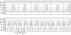
도 5는 본 발명의 일 실시예에 의한 스위칭 모드 전원공급장치의 구동을 설명하기 위한 파형도이다. 특히, 도 5의 상단부의 그래프는 도 3의 P1 포트에서 검출한 스위칭 신호를 도시한 그래프이고, 하단부의 그래프는 도 5의 P2 포트에서 검출한 원시 스위칭 신호를 도시한 그래프이다.5 is a waveform diagram illustrating the driving of a switching mode power supply apparatus according to an embodiment of the present invention. In particular, the graph of the upper part of FIG. 5 is a graph showing the switching signal detected by the P1 port of FIG. 3, and the graph of the lower part is a graph showing the original switching signal detected by the P2 port of FIG. 5.
도 3 및 도 5를 참조하면, 대기 모드의 경우 제2 충전부(C2)에 의해 공진 회로부(240)는 가변 공진 주파수를 갖게 되고, 이에 의해 원시 스위칭 신호는 도 7에 도시된 원시 스위칭 신호에 비해 그 시비율이 가변된다. 즉, 도 7의 비교예에서는 각 펄스의 시비율은 동일한 시비율로 형성되고, 이에 의해 0 전위로 신호 제어부(260)에서 인식하는 구간(C)이 증가하게 된다.3 and 5, in the standby mode, the
예를 들어, 본 실시예에서와 같이 신호 제어부(260)가 "NCP1207" 콘트롤러로 구성되는 경우, 0 전위가 검출된 후 8us의 지연 시간 동안 그 이상의 전위가 검출되지 아니하면 스위칭 신호를 출력하게 된다. 따라서, 비교예에 도시된 바와 같이 각 원시 스위칭 신호에 대해 8us 시간 후에 스위칭 신호가 출력된다.For example, when the
반면, 도 5를 참조하면, 가변 공진 주파수에 의해 원시 스위칭 신호의 고조파 성분이 소정 시간동안 지연되어 출력하기 때문에 0 전위가 검출되는 시간을 소정 시간동안 지연시킬 수 있고, 이에 따라 콘트롤러가 인식 가능한 시간 예를 들어, 0 전위가 검출된 후 8us의 시간 이하의 지연 시간 중 그 이상의 전위가 검출되는 구간(A)이 형성되어 이 구간에서는 원시 스위칭 신호에 의해 스위칭 신호가 출력되는 것이 차단된다. 그러나, 8us의 시간 이하의 지연 시간동안 그 이상의 전위가 검출되지 아니하는 구간(B) 구간에서는 원시 스위칭 신호에 의해 스위칭 신호가 출력된다.On the other hand, referring to FIG. 5, since the harmonic components of the source switching signal are delayed and output for a predetermined time by the variable resonant frequency, the time at which the zero potential is detected can be delayed for a predetermined time, and thus the controller can recognize the time. For example, after the zero potential is detected, a section A in which more potentials are detected among a delay time of 8 us or less is formed, and in this section, the output of the switching signal is blocked by the raw switching signal. However, the switching signal is output by the raw switching signal in the section B in which no more potential is detected during the delay time of 8 us or less.
따라서, 본 실시예에 의하면, 제2 충전부(C2)의 커패시턴스를 조절함으로써, 그 고조파 성분의 시비율을 가변적으로 형성함으로써, 0 전위 이하의 원시 스위칭 신호가 신호 검출부(260)로 출력되는 시간을 조절하여, 신호 검출부(260)가 각 원시 스위칭 신호에 0 전위 검출 구간에서 스위칭 신호를 출력하는 것을 차단할 수 있다.Therefore, according to the present embodiment, by adjusting the capacitance of the second charging unit C2 to variably form the ratio of the harmonic components, the time for outputting the source switching signal below zero potential to the
이에 의해, 스위칭 신호의 주파수를 낮은 주파수로 형성되고, 주파수와 비례하여 증가하는 EMI 및 각 스위칭 신호에 의한 스위칭 동작이 수행될 때, 모스 트랜지스터(M_TR)에서 발생하는 전력 손실이 방지된다.As a result, when the frequency of the switching signal is formed at a low frequency and EMI is increased in proportion to the frequency and switching operation by each switching signal is performed, power loss occurring in the MOS transistor M_TR is prevented.
상기한 바와 같이 본 발명에 의하면, 준 공진 제어 방식에서 부하단의 임피던스가 낮아질 때, 고조파 성분에 의해 스위칭 신호 주파수의 증가에 비례하는 EMI 특성 저하를 방지할 수 있다.As described above, according to the present invention, when the impedance of the load stage is lowered in the quasi-resonant control method, it is possible to prevent the EMI characteristic deterioration in proportion to the increase in the switching signal frequency by the harmonic component.
또한, 스위칭 신호의 주파수가 증가되어 스위칭 트랜지스터의 스위칭 동작의 증가함에 따른 전력 손실을 방지할 수 있다.In addition, the frequency of the switching signal is increased to prevent power loss due to an increase in the switching operation of the switching transistor.
상기에서는 본 발명의 바람직한 실시예를 참조하여 설명하였지만, 해당 분야의 숙련된 당업자는 하기의 특허 청구의 범위에 기재된 본 발명의 사상 및 영역으로부터 벗어나지 않는 범위 내에서 본 발명을 다양하게 수정 및 변경시킬 수 있음을 이해할 수 있을 것이다.While the foregoing has been described with reference to preferred embodiments of the invention, those skilled in the art will be able to make various modifications and changes to the invention without departing from the spirit and scope of the invention as set forth in the claims below. It will be appreciated.
Claims (19)
Translated fromKoreanPriority Applications (5)
| Application Number | Priority Date | Filing Date | Title |
|---|---|---|---|
| KR1020060073646AKR101248910B1 (en) | 2006-08-04 | 2006-08-04 | Switching mode power supply and image forming device having the same and method of driving thereof |
| US11/692,455US7791908B2 (en) | 2006-08-04 | 2007-03-28 | Switching mode power supply (SMPS) device, image forming apparatus including the SMPS device, and method of driving the SMPS device |
| EP07107832.3AEP1885052B1 (en) | 2006-08-04 | 2007-05-09 | Switching Mode Power Supply (SMPS) device, image forming apparatus including the SMPS device, and method of driving the SMPS device |
| CN2007101042919ACN101119071B (en) | 2006-08-04 | 2007-05-25 | Switching mode power supply device, image forming apparatus and driving method thereof |
| CN201210277235.6ACN102801332B (en) | 2006-08-04 | 2007-05-25 | Switch mode power supply and driving method thereof |
Applications Claiming Priority (1)
| Application Number | Priority Date | Filing Date | Title |
|---|---|---|---|
| KR1020060073646AKR101248910B1 (en) | 2006-08-04 | 2006-08-04 | Switching mode power supply and image forming device having the same and method of driving thereof |
Publications (2)
| Publication Number | Publication Date |
|---|---|
| KR20080012595A KR20080012595A (en) | 2008-02-12 |
| KR101248910B1true KR101248910B1 (en) | 2013-03-28 |
Family
ID=38740180
Family Applications (1)
| Application Number | Title | Priority Date | Filing Date |
|---|---|---|---|
| KR1020060073646AExpired - Fee RelatedKR101248910B1 (en) | 2006-08-04 | 2006-08-04 | Switching mode power supply and image forming device having the same and method of driving thereof |
Country Status (4)
| Country | Link |
|---|---|
| US (1) | US7791908B2 (en) |
| EP (1) | EP1885052B1 (en) |
| KR (1) | KR101248910B1 (en) |
| CN (2) | CN101119071B (en) |
Cited By (1)
| Publication number | Priority date | Publication date | Assignee | Title |
|---|---|---|---|---|
| KR20160023091A (en) | 2014-08-21 | 2016-03-03 | 한국전기연구원 | Switched Mode Power Supply |
Families Citing this family (13)
| Publication number | Priority date | Publication date | Assignee | Title |
|---|---|---|---|---|
| US8239694B2 (en)* | 2008-03-31 | 2012-08-07 | Qualcomm, Incorporated | Dynamic frequency scaling of a switched mode power supply |
| US8258768B2 (en)* | 2008-12-12 | 2012-09-04 | Schneider Electric USA, Inc. | Low EMI producing switch-mode power supply within an intelligent electronic device |
| KR101023381B1 (en) | 2009-06-01 | 2011-03-18 | 삼성전기주식회사 | Adapter power unit |
| KR101757460B1 (en)* | 2010-07-05 | 2017-07-12 | 에스프린팅솔루션 주식회사 | Switching mode power supply and method of supplying power by using the same |
| JP5610947B2 (en)* | 2010-09-17 | 2014-10-22 | キヤノン株式会社 | Power supply circuit and image forming apparatus having the same |
| JP5654817B2 (en) | 2010-09-22 | 2015-01-14 | キヤノン株式会社 | Image forming apparatus |
| SG191053A1 (en)* | 2010-12-09 | 2013-08-30 | Indice Pty Ltd | Power supply control system and device |
| CN102916586B (en) | 2011-08-04 | 2014-04-02 | 昂宝电子(上海)有限公司 | Systems and methods for switching power converters |
| RU2624453C2 (en)* | 2011-10-18 | 2017-07-04 | Филипс Лайтинг Холдинг Б.В. | Split beam lighting device and lighting system |
| EP2717449B1 (en)* | 2012-10-05 | 2016-12-14 | Nxp B.V. | Isolated switched-mode power supply |
| CN105048822B (en)* | 2013-08-29 | 2019-03-01 | 昂宝电子(上海)有限公司 | The system and method for adjusting frequency and electric current based on loading condition |
| CN106253686B (en)* | 2016-08-24 | 2018-07-03 | 华中科技大学 | A kind of excitation power supply for being used to inhibit laser pulse overshoot phenomenon |
| CN109830948B (en)* | 2017-11-23 | 2023-01-06 | 丰郅(上海)新能源科技有限公司 | Power processing system and power processing method |
Citations (4)
| Publication number | Priority date | Publication date | Assignee | Title |
|---|---|---|---|---|
| JPH11155281A (en)* | 1997-09-22 | 1999-06-08 | Seiko Instruments Inc | Switching regulator |
| US6038144A (en) | 1998-03-27 | 2000-03-14 | Murata Manufacturing Co., Ltd. | DC-DC converter |
| US6154015A (en) | 1998-07-14 | 2000-11-28 | Ricoh Company, Ltd. | DC-DC converter |
| JP2005287244A (en)* | 2004-03-30 | 2005-10-13 | Brother Ind Ltd | Power supply device and image forming apparatus |
Family Cites Families (8)
| Publication number | Priority date | Publication date | Assignee | Title |
|---|---|---|---|---|
| GB2199454B (en)* | 1986-11-29 | 1990-10-03 | Toshiba Kk | Induction heated cooking apparatus |
| KR0133633B1 (en)* | 1994-07-21 | 1998-04-23 | 이형도 | Switching mode power supply circuit with output voltage control and overcurrent protection |
| US6408148B1 (en)* | 1999-05-17 | 2002-06-18 | Canon Kabushiki Kaisha | Image processing apparatus, image recording apparatus, controlling method for these apparatuses, and power supply apparatus used therein |
| JP4314709B2 (en)* | 1999-12-28 | 2009-08-19 | ソニー株式会社 | Switching power supply |
| US6545451B2 (en)* | 2000-08-28 | 2003-04-08 | Delta Electronics, Inc. | Load-dependent frequency modulation circuit and method for switching power system |
| US6480401B2 (en)* | 2001-03-13 | 2002-11-12 | Astec International Limited | Method and apparatus for reducing standby power in power supplies |
| JP2003299347A (en)* | 2002-02-01 | 2003-10-17 | Seiko Instruments Inc | Pwm switching regulator control circuit, pwm switching regulator and electronic component |
| JP3636321B2 (en)* | 2002-04-24 | 2005-04-06 | ローム株式会社 | Switching power supply |
- 2006
- 2006-08-04KRKR1020060073646Apatent/KR101248910B1/ennot_activeExpired - Fee Related
- 2007
- 2007-03-28USUS11/692,455patent/US7791908B2/ennot_activeExpired - Fee Related
- 2007-05-09EPEP07107832.3Apatent/EP1885052B1/ennot_activeNot-in-force
- 2007-05-25CNCN2007101042919Apatent/CN101119071B/ennot_activeExpired - Fee Related
- 2007-05-25CNCN201210277235.6Apatent/CN102801332B/ennot_activeExpired - Fee Related
Patent Citations (4)
| Publication number | Priority date | Publication date | Assignee | Title |
|---|---|---|---|---|
| JPH11155281A (en)* | 1997-09-22 | 1999-06-08 | Seiko Instruments Inc | Switching regulator |
| US6038144A (en) | 1998-03-27 | 2000-03-14 | Murata Manufacturing Co., Ltd. | DC-DC converter |
| US6154015A (en) | 1998-07-14 | 2000-11-28 | Ricoh Company, Ltd. | DC-DC converter |
| JP2005287244A (en)* | 2004-03-30 | 2005-10-13 | Brother Ind Ltd | Power supply device and image forming apparatus |
Cited By (1)
| Publication number | Priority date | Publication date | Assignee | Title |
|---|---|---|---|---|
| KR20160023091A (en) | 2014-08-21 | 2016-03-03 | 한국전기연구원 | Switched Mode Power Supply |
Also Published As
| Publication number | Publication date |
|---|---|
| CN101119071A (en) | 2008-02-06 |
| EP1885052B1 (en) | 2019-09-25 |
| KR20080012595A (en) | 2008-02-12 |
| US20080031015A1 (en) | 2008-02-07 |
| EP1885052A2 (en) | 2008-02-06 |
| CN102801332A (en) | 2012-11-28 |
| EP1885052A3 (en) | 2015-09-23 |
| CN101119071B (en) | 2012-09-26 |
| CN102801332B (en) | 2015-11-04 |
| US7791908B2 (en) | 2010-09-07 |
Similar Documents
| Publication | Publication Date | Title |
|---|---|---|
| KR101248910B1 (en) | Switching mode power supply and image forming device having the same and method of driving thereof | |
| EP2637295B1 (en) | Power supply device and image forming apparatus | |
| US7933131B2 (en) | Power supply and image forming device having the same | |
| JP5885399B2 (en) | Switching power supply | |
| US8116104B2 (en) | Power supply apparatus with noise attenuator to reduce harmonic current and electronic device having the power supply apparatus | |
| US10536085B2 (en) | Power supply apparatus and image forming apparatus | |
| JP6949567B2 (en) | Image forming device | |
| JP2015104281A (en) | Power supply device and image forming apparatus | |
| JP2015018633A (en) | Induction heating apparatus, induction heating fixing apparatus, and image forming apparatus | |
| JP2019004541A5 (en) | ||
| KR101436967B1 (en) | Current resonance power supply | |
| KR100695735B1 (en) | Resonant power supply | |
| JP6098311B2 (en) | Power supply device and image forming apparatus | |
| US9525359B2 (en) | Switching power supply apparatus and image forming apparatus | |
| JP3568870B2 (en) | converter | |
| US6580624B2 (en) | Switching power circuit with a filter for controlling noise of a switching frequency and method of same | |
| US20070013409A1 (en) | Digitally controlled high-voltage power supply and method therefor | |
| JP7182983B2 (en) | Power supply and image forming apparatus | |
| JP5972186B2 (en) | Power supply device and image forming apparatus provided with the same | |
| JP2018064387A (en) | Image forming apparatus | |
| KR20050108281A (en) | Switching mode power supply | |
| JP2001008453A (en) | Switching power supply device |
Legal Events
| Date | Code | Title | Description |
|---|---|---|---|
| PA0109 | Patent application | St.27 status event code:A-0-1-A10-A12-nap-PA0109 | |
| PG1501 | Laying open of application | St.27 status event code:A-1-1-Q10-Q12-nap-PG1501 | |
| A201 | Request for examination | ||
| PA0201 | Request for examination | St.27 status event code:A-1-2-D10-D11-exm-PA0201 | |
| R18-X000 | Changes to party contact information recorded | St.27 status event code:A-3-3-R10-R18-oth-X000 | |
| PE0902 | Notice of grounds for rejection | St.27 status event code:A-1-2-D10-D21-exm-PE0902 | |
| P11-X000 | Amendment of application requested | St.27 status event code:A-2-2-P10-P11-nap-X000 | |
| P13-X000 | Application amended | St.27 status event code:A-2-2-P10-P13-nap-X000 | |
| E701 | Decision to grant or registration of patent right | ||
| PE0701 | Decision of registration | St.27 status event code:A-1-2-D10-D22-exm-PE0701 | |
| GRNT | Written decision to grant | ||
| PR0701 | Registration of establishment | St.27 status event code:A-2-4-F10-F11-exm-PR0701 | |
| PR1002 | Payment of registration fee | St.27 status event code:A-2-2-U10-U11-oth-PR1002 Fee payment year number:1 | |
| PG1601 | Publication of registration | St.27 status event code:A-4-4-Q10-Q13-nap-PG1601 | |
| FPAY | Annual fee payment | Payment date:20160226 Year of fee payment:4 | |
| PR1001 | Payment of annual fee | St.27 status event code:A-4-4-U10-U11-oth-PR1001 Fee payment year number:4 | |
| PN2301 | Change of applicant | St.27 status event code:A-5-5-R10-R11-asn-PN2301 | |
| PN2301 | Change of applicant | St.27 status event code:A-5-5-R10-R14-asn-PN2301 | |
| FPAY | Annual fee payment | Payment date:20170223 Year of fee payment:5 | |
| PR1001 | Payment of annual fee | St.27 status event code:A-4-4-U10-U11-oth-PR1001 Fee payment year number:5 | |
| PR1001 | Payment of annual fee | St.27 status event code:A-4-4-U10-U11-oth-PR1001 Fee payment year number:6 | |
| PN2301 | Change of applicant | St.27 status event code:A-5-5-R10-R13-asn-PN2301 St.27 status event code:A-5-5-R10-R11-asn-PN2301 | |
| PN2301 | Change of applicant | St.27 status event code:A-5-5-R10-R13-asn-PN2301 St.27 status event code:A-5-5-R10-R11-asn-PN2301 | |
| PR1001 | Payment of annual fee | St.27 status event code:A-4-4-U10-U11-oth-PR1001 Fee payment year number:7 | |
| PN2301 | Change of applicant | St.27 status event code:A-5-5-R10-R11-asn-PN2301 | |
| PN2301 | Change of applicant | St.27 status event code:A-5-5-R10-R14-asn-PN2301 | |
| PR1001 | Payment of annual fee | St.27 status event code:A-4-4-U10-U11-oth-PR1001 Fee payment year number:8 | |
| PC1903 | Unpaid annual fee | St.27 status event code:A-4-4-U10-U13-oth-PC1903 Not in force date:20210322 Payment event data comment text:Termination Category : DEFAULT_OF_REGISTRATION_FEE | |
| PC1903 | Unpaid annual fee | St.27 status event code:N-4-6-H10-H13-oth-PC1903 Ip right cessation event data comment text:Termination Category : DEFAULT_OF_REGISTRATION_FEE Not in force date:20210322 |