KR101246191B1 - Plasma generation apparatus and substrate processing apparatus - Google Patents
Plasma generation apparatus and substrate processing apparatusDownload PDFInfo
- Publication number
- KR101246191B1 KR101246191B1KR1020110104792AKR20110104792AKR101246191B1KR 101246191 B1KR101246191 B1KR 101246191B1KR 1020110104792 AKR1020110104792 AKR 1020110104792AKR 20110104792 AKR20110104792 AKR 20110104792AKR 101246191 B1KR101246191 B1KR 101246191B1
- Authority
- KR
- South Korea
- Prior art keywords
- group
- antennas
- power
- disposed
- power source
- Prior art date
- Legal status (The legal status is an assumption and is not a legal conclusion. Google has not performed a legal analysis and makes no representation as to the accuracy of the status listed.)
- Active
Links
Images


Classifications
- H—ELECTRICITY
- H01—ELECTRIC ELEMENTS
- H01J—ELECTRIC DISCHARGE TUBES OR DISCHARGE LAMPS
- H01J37/00—Discharge tubes with provision for introducing objects or material to be exposed to the discharge, e.g. for the purpose of examination or processing thereof
- H01J37/32—Gas-filled discharge tubes
- H01J37/32009—Arrangements for generation of plasma specially adapted for examination or treatment of objects, e.g. plasma sources
- H01J37/32082—Radio frequency generated discharge
- H01J37/321—Radio frequency generated discharge the radio frequency energy being inductively coupled to the plasma
- H01J37/3211—Antennas, e.g. particular shapes of coils
- H—ELECTRICITY
- H05—ELECTRIC TECHNIQUES NOT OTHERWISE PROVIDED FOR
- H05H—PLASMA TECHNIQUE; PRODUCTION OF ACCELERATED ELECTRICALLY-CHARGED PARTICLES OR OF NEUTRONS; PRODUCTION OR ACCELERATION OF NEUTRAL MOLECULAR OR ATOMIC BEAMS
- H05H1/00—Generating plasma; Handling plasma
- H05H1/24—Generating plasma
- H05H1/46—Generating plasma using applied electromagnetic fields, e.g. high frequency or microwave energy
- H—ELECTRICITY
- H01—ELECTRIC ELEMENTS
- H01J—ELECTRIC DISCHARGE TUBES OR DISCHARGE LAMPS
- H01J37/00—Discharge tubes with provision for introducing objects or material to be exposed to the discharge, e.g. for the purpose of examination or processing thereof
- H01J37/32—Gas-filled discharge tubes
- H01J37/32009—Arrangements for generation of plasma specially adapted for examination or treatment of objects, e.g. plasma sources
- H01J37/32082—Radio frequency generated discharge
- H01J37/32137—Radio frequency generated discharge controlling of the discharge by modulation of energy
- H01J37/32155—Frequency modulation
- H01J37/32165—Plural frequencies
- H—ELECTRICITY
- H05—ELECTRIC TECHNIQUES NOT OTHERWISE PROVIDED FOR
- H05H—PLASMA TECHNIQUE; PRODUCTION OF ACCELERATED ELECTRICALLY-CHARGED PARTICLES OR OF NEUTRONS; PRODUCTION OR ACCELERATION OF NEUTRAL MOLECULAR OR ATOMIC BEAMS
- H05H1/00—Generating plasma; Handling plasma
- H05H1/24—Generating plasma
- H05H1/26—Plasma torches
- H05H1/32—Plasma torches using an arc
- H05H1/34—Details, e.g. electrodes, nozzles
- H05H1/36—Circuit arrangements
- H—ELECTRICITY
- H05—ELECTRIC TECHNIQUES NOT OTHERWISE PROVIDED FOR
- H05H—PLASMA TECHNIQUE; PRODUCTION OF ACCELERATED ELECTRICALLY-CHARGED PARTICLES OR OF NEUTRONS; PRODUCTION OR ACCELERATION OF NEUTRAL MOLECULAR OR ATOMIC BEAMS
- H05H1/00—Generating plasma; Handling plasma
- H05H1/24—Generating plasma
- H05H1/46—Generating plasma using applied electromagnetic fields, e.g. high frequency or microwave energy
- H05H1/4645—Radiofrequency discharges
- H05H1/4652—Radiofrequency discharges using inductive coupling means, e.g. coils
- H—ELECTRICITY
- H01—ELECTRIC ELEMENTS
- H01J—ELECTRIC DISCHARGE TUBES OR DISCHARGE LAMPS
- H01J2237/00—Discharge tubes exposing object to beam, e.g. for analysis treatment, etching, imaging
- H01J2237/32—Processing objects by plasma generation
- H01J2237/327—Arrangements for generating the plasma
Landscapes
- Physics & Mathematics (AREA)
- Engineering & Computer Science (AREA)
- Plasma & Fusion (AREA)
- Spectroscopy & Molecular Physics (AREA)
- Chemical & Material Sciences (AREA)
- Analytical Chemistry (AREA)
- Electromagnetism (AREA)
- Plasma Technology (AREA)
Abstract
Translated fromKoreanDescription
Translated fromKorean본 발명은 플라즈마 발생 장치에 관한 것으로, 더 구체적으로 복수의 안테나를 사용하는 유도 결합 플라즈마 발생 장치에 관한 것이다.Field of the Invention [0002] The present invention relates to a plasma generating apparatus, and more particularly, to an inductively coupled plasma generating apparatus using a plurality of antennas.
본 발명은 플라즈마 발생 장치에 관한 것으로, 더 구체적으로 유도 결합 플라즈마 발생 장치에 관한 것이다.The present invention relates to a plasma generating apparatus, and more particularly to an inductively coupled plasma generating apparatus.
본 발명의 해결하고자 하는 일 기술적 과제는 균일한 헬리콘 또는 유도 결합 플라즈마를 형성하는 플라즈마 발생 장치를 제공하는 것이다.SUMMARY OF THE INVENTION It is an object of the present invention to provide a plasma generating apparatus for forming a uniform helicon or inductively coupled plasma.
본 발명의 일 실시예에 따른 플라즈마 발생 장치는 진공 용기에 형성된 복수의 관통홀들에 각각 장착되는 복수의 유전체 튜브들; 상기 진공 용기에 배치되는 대칭성에 따라 제1 그룹 및 제2 그룹으로 분류되고 상기 유전체 튜브들의 외측에 각각 장착되는 안테나들; 상기 제1 그룹의 안테나에 전력을 공급하는 제1 RF 전원;상기 제2 그룹의 안테나에 전력을 공급하는 제2 RF 전원; 및 상기 제1 그룹의 안테나와 상기 제1 RF 전원 사이에 배치되어 상기 제1 RF 전원의 전력을 상기 제1 그룹의 안테나에 전력을 분배하는 제1 전력 분배부를 포함한다.A plasma generating apparatus according to an embodiment of the present invention comprises a plurality of dielectric tubes mounted in each of a plurality of through holes formed in a vacuum container; Antennas, each classified into a first group and a second group according to symmetry disposed in the vacuum container, and mounted to the outside of the dielectric tubes; A first RF power supply for supplying power to the antennas of the first group; a second RF power supply for supplying power to the antennas of the second group; And a first power distribution unit disposed between the first group of antennas and the first RF power source to distribute power to the antennas of the first group.
본 발명의 일 실시예에 있어서, 상기 제1 전력 분배부는 제1 전력 분배 라인; 및 상기 제1 전력 분배 라인을 감싸고 접지되는 제1 도전성 외피를 포함하고, 상기 제1 전력 분배부의 입력단과 상기 제1 그룹의 안테나 사이의 거리는 동일할 수 있다.In one embodiment of the present invention, the first power distribution unit comprises: a first power distribution line; And a first conductive envelope surrounding and grounding the first power distribution line, wherein a distance between an input terminal of the first power distribution unit and the antenna of the first group may be the same.
본 발명의 일 실시예에 있어서, 상기 제2 RF 전원과 상기 제2 그룹의 안테나 사이에 배치되는 상기 제2 전력 분배부를 더 포함하고, 상기 제2 전력 분배부는:In one embodiment of the present invention, the second power divider further comprises a second power divider disposed between the second RF power source and the second group of antennas, wherein the second power divider comprises:
제2 전력 분배 라인; 및 상기 제2 전력 분배 라인을 감싸고 접지되는 제2 도전성 외피를 포함하고, 상기 제2 전력 분배부의 입력단과 상기 제2 그룹의 안테나 사이의 거리는 동일할 수 있다.A second power distribution line; And a second conductive envelope surrounding and grounding the second power distribution line, wherein a distance between an input terminal of the second power distribution unit and the antenna of the second group may be the same.
본 발명의 일 실시예에 있어서, 상기 유전체 튜브들의 길이 방향으로 이격되어 배치되는 토로이드 형태의 영구 자석들을 더 포함할 수 있다.In an embodiment of the present invention, the dielectric tubes may further include toroidal permanent magnets spaced apart from each other in the longitudinal direction.
본 발명의 일 실시예에 있어서, 상기 영구 자석들의 전부 또는 일부를 고정하고 상기 영구 자석들이 배치되는 평면을 이동시키는 이동부를 더 포함할 수 있다.In one embodiment of the present invention, it may further include a moving part for fixing all or part of the permanent magnets and to move the plane in which the permanent magnets are disposed.
본 발명의 일 실시예에 있어서, 상기 이동부는 상기 진공 용기에 고정 결합하고 상기 유전체 튜브들이 배치된 평면에 수직하게 연장되는 적어도 하나의 지지 기둥; 및 상기 영구 자석들이 장착되고 상기 지지 기둥에 삽입되어 상기 지지 기둥을 따라 이동 가능한 영구 자석 고정판을 포함할 수 있다.In one embodiment of the present invention, the moving part is fixedly coupled to the vacuum container and at least one support pillar extending perpendicular to the plane in which the dielectric tubes are disposed; And a permanent magnet fixing plate mounted with the permanent magnets and inserted into the support pillar and movable along the support pillar.
본 발명의 일 실시예에 있어서, 상기 제1 그룹의 안테나들은 상기 진공 용기의 원형의 상판의 중심을 기준으로 일정한 반경의 원주의 주위에 대칭적으로 되고,상기 제2 그룹의 안테나는 상기 상판의 중심에 배치될 수 있다.In one embodiment of the invention, the antennas of the first group are symmetrical around a circumference of a constant radius with respect to the center of the circular top plate of the vacuum vessel, and the antennas of the second group are It can be placed in the center.
본 발명의 일 실시예에 있어서, 상기 제1 전력 분배부는 상기 제1 RF 전원으로터 전력을 공급받는 동축 케이블 형태의 입력 브랜치; 상기 입력 브랜치와 연결되고 3 갈래로 갈라지는 동축 케이블 형태의 3 웨이(way) 브랜치; 및 상기 3 웨이 브랜치에 연결되어 2 갈래로 갈라지는 동축 케이블 형태의 T 브랜치들을 포함할 수 있다.In one embodiment of the present invention, the first power distribution unit comprises: an input branch in the form of a coaxial cable that receives power from the first RF power source; A three-way branch in the form of a coaxial cable connected to the input branch and split into three branches; And T branches in the form of coaxial cables divided into two branches connected to the three-way branch.
본 발명의 일 실시예에 있어서, 상기 안테나들을 고정하고 상기 상판에 고정되는 고정판들; 및 상기 고정판과 상기 T 브랜치들의 외측 도선을 연결하는 접지 라인을 더 포함하고, 상기 고정판들의 일단은 상기 안테나들을 통하여 상기 T 브랜치들의 내측 도선에 연결되고, 상기 고정판들의 타단은 상기 접지 라인에 연결되고, 상기 접지 라인의 길이는 모든 안테나들에 대하여 동일할 수 있다.In one embodiment of the present invention, fixing the antenna and fixed to the top plate; And a ground line connecting the fixing plate and the outer conductorsof the T branches, one end of the fixing plates being connected to the inner conductor of the T branches via the antennas, and the other end of the fixing plates being connected to the ground line. The length of the ground line may be the same for all antennas.
본 발명의 일 실시예에 있어서, 상기 유전체 튜브들의 일단에 각각 장착되는 금속 뚜껑들을 더 포함하고, 상기 유전체 듀브들의 길이(L/2=π/kz)은In one embodiment of the invention, further comprises metal lids each mounted to one end of the dielectric tubes, the length of the dielectric dubes (L / 2 = π / kz ) is

조건을 만족하고, R은 상기 유전체 튜브들의 반경이고, B0는 상기 유전체 튜브들의 중심에서 자속 밀도의 세기이고, μ0는 투자율이이고, ω는 각주파수이고, n0은 플라즈마의 밀도일 수 있다.Condition is met, R is the radius of the dielectric tubes, B0 is the strength of the magnetic flux density at the center of the dielectric tubes, μ0 is the permeability, ω is the angular frequency, n0 is the density of the plasma have.
본 발명의 일 실시예에 있어서, 상기 제1 RF 전원의 구동 주파수는 상기 제2 RF 전원의 구동 주파수와 서로 다를 수 있다.In one embodiment of the present invention, the driving frequency of the first RF power source may be different from the driving frequency of the second RF power source.
본 발명의 일 실시예에 있어서, 상기 안테나들은 상기 진공 용기의 사각형의 상판에 매트릭스 형태로 배치되고, 상기 제1 그룹의 안테나는 외곽을 따라 배치되고, 상기 제2 그룹의 안테나는 상기 제1 그룹의 안테나로 둘러싸이도록 내측에 배치될 수 있다.In one embodiment of the present invention, the antennas are arranged in a matrix form on the rectangular top plate of the vacuum vessel, the antennas of the first group is disposed along the outside, the antennas of the second group is the first group It may be disposed inside so as to be surrounded by an antenna.
본 발명의 일 실시예에 있어서, 상기 제2 그룹의 안테나와 상기 제2 RF 전원 사이에 배치되어, 상기 제2 RF 전원의 전력은 상기 제2 그룹의 안테나에 분배하는 제2 전력 분배부를 더 포함할 수 있다.In one embodiment of the present invention, the second RF power supply disposed between the antenna and the second RF power supply, further comprising a second power distribution unit for distributing the power of the second RF power to the antenna of the second group. can do.
본 발명의 일 실시예에 따른 기판 처리 장치는 진공 용기에 형성된 복수의 관통홀들에 각각 장착되는 복수의 유전체 튜브들; 상기 진공 용기에 배치되는 대칭성에 따라 제1 그룹 및 제2 그룹으로 분류되고 상기 유전체 튜브들의 외측에 각각 장착되는 안테나들; 상기 제1 그룹의 안테나에 전력을 공급하는 제1 RF 전원;A substrate processing apparatus according to an embodiment of the present invention includes a plurality of dielectric tubes mounted in a plurality of through holes formed in a vacuum container, respectively; Antennas, each classified into a first group and a second group according to symmetry disposed in the vacuum container, and mounted to the outside of the dielectric tubes; A first RF power source for supplying power to said first group of antennas;
상기 제2 그룹의 안테나에 전력을 공급하는 제2 RF 전원; 및 상기 제1 그룹의 안테나와 상기 제1 RF 전원 사이에 배치되어 상기 제1 RF 전원의 전력을 상기 제1 그룹의 안테나에 전력을 분배하는 제1 전력 분배부를 포함할 수 있다.A second RF power source for powering the second group of antennas; And a first power distribution unit disposed between the first group of antennas and the first RF power source to distribute the power of the first RF power source to the antennas of the first group.
본 발명의 일 실시예에 있어서, 상기 관통홀들의 하부에 배치된 그리드들을 더 포함할 수 있다.In one embodiment of the present invention, it may further include grids disposed under the through holes.
본 발명의 일 실시예에 따른 플라즈마 발생 장치는 헬리콘 플라즈마를 공간적으로 균일하게 형성할 수 있다.Plasma generator according to an embodiment of the present invention can form a spatially uniform helicon plasma.
도 1은 본 발명의 일 실시예에 따른 플라즈마 발생 장치를 설명하는 사시도이다.
도 2는 도 1의 유전체 튜브들의 배치관계를 설명하는 평면도이다.
도 3은 도 1의 플라즈마 발생 장치를 설명하는 개념도이다.
도 4는 도 1의 플라즈마 발생 장치를 설명하는 회로도이다.
도 5는 도 1의 유전체 튜브들를 설명하는 도면이다.
도 6a은 도 1의 전력 분배부를 설명하는 사시도이다.
도 6b는 도 6a의 I-I'선을 따라 자른 단면도이다.
도 6c는 도 6a의 II-II'선을 따라 자른 단면도이다.
도 6d는 도 6a의 III-III'선을 따라 자른 단면도이다.
도 7은 본 발명의 다른 실시예에 따른 플라즈마 발생 장치를 설명하는 평면도이다.
도 8은 도 7의 플라즈마 발생 장치의 회로도이다.
도 9는 본 발명의 또 다른 실시예에 따른 플라즈마 발생 장치를 설명하는 도면이다.1 is a perspective view illustrating a plasma generating apparatus according to an embodiment of the present invention.
2 is a plan view illustrating an arrangement relationship of the dielectric tubes of FIG. 1.
3 is a conceptual diagram illustrating the plasma generating apparatus of FIG. 1.
4 is a circuit diagram illustrating the plasma generation device of FIG. 1.
5 is a diagram illustrating the dielectric tubes of FIG. 1.
6A is a perspective view illustrating the power distribution unit of FIG. 1.
FIG. 6B is a cross-sectional view taken along the line II ′ of FIG. 6A.
FIG. 6C is a cross-sectional view taken along the line II-II 'of FIG. 6A.
FIG. 6D is a cross-sectional view taken along the line III-III ′ of FIG. 6A.
7 is a plan view illustrating a plasma generating apparatus according to another embodiment of the present invention.
FIG. 8 is a circuit diagram of the plasma generator of FIG. 7.
9 is a view for explaining a plasma generating apparatus according to another embodiment of the present invention.
대면적 플라즈마를 형성하기 위하여, 하나의 전원은 병렬 연결된 복수의 안테나들에 전력을 공급할 수 있다. 전력 분배부는 안테나들과 전원 사이에 배치되어 각 안테나들에 동일한 전력을 공급할 수 있다.In order to form a large area plasma, one power source can power a plurality of antennas connected in parallel. The power distribution unit may be disposed between the antennas and the power supply to supply the same power to each antenna.
예를 들어, 진공 용기의 원형 상판에 7 개의 안테나들이 배치되고, 하나는 상판의 중심에 배치되고, 나머지 6 개는 상기 중심을 기준으로 하는 소정의 원주 상에 대칭적으로 배치될 수 있다. 상기 7 개의 안테나들은 상기 전력 분배부를 통하여 하나의 전원에 연결될 수 있다.For example, seven antennas may be arranged on a circular top plate of a vacuum vessel, one may be disposed at the center of the top plate, and the other six may be symmetrically disposed on a predetermined circumference based on the center. The seven antennas may be connected to one power source through the power distribution unit.
그러나, 안테나들이 플라즈마를 형성하는 경우, 대칭성을 가진 원주 상의 안테나들의 임피던스와 중심의 안테나의 임피던스는 서로 다르게 된다. 따라서, 일부의 안테나들에 전력이 집중되어 균일한 플라즈마가 형성될 수 없다.However, when the antennas form a plasma, the impedances of the symmetrical circumferential antennas and the central antennas are different from each other. Therefore, power is concentrated in some antennas and a uniform plasma cannot be formed.
따라서, 본 발명의 일 실시예에 따른 플라즈마 발생 장치에서는 안테나들의 배치 대칭성에 따라 안테나들은 복수의 안테나 그룹으로 분류되고, 각 안테나 그룹은 서로 다른 전원에 연결되어 안테나 그룹 간에 독립적인 전력을 공급될 수 있다.Therefore, in the plasma generating apparatus according to an embodiment of the present invention, the antennas are classified into a plurality of antenna groups according to the arrangement symmetry of the antennas, and each antenna group may be connected to different power sources to supply independent power between the antenna groups. have.
또한, 전력 분배부는 각 안테나 그룹 내의 모든 안테나들에 동일한 길이를 가지는 동축 케이블 형태를 가진다. 따라서, 각 안테나 그룹 내의 모든 안테나들은 동일한 조건에서 동작될 수 있다.In addition, the power distribution unit has the form of a coaxial cable having the same length for all antennas in each antenna group. Thus, all antennas in each antenna group can be operated under the same conditions.
유도 결합 플라즈마 장치는 통상적으로 수십 밀리토르(mTorr) 이상에서 고밀도 플라즈마를 생성한다. 하지만, 상기 유도 결합 플라즈마 장치는 수 밀리토르(mTorr)의 저압에서 고밀도 플라즈마를 생성하기 어렵다. 따라서, 하나의 진공 용기 내에서 저압 공정 및 고압 공정은 연속적으로 수행될 수 없었다.Inductively coupled plasma devices typically produce high density plasma at tens of milliTorr (mTorr) or higher. However, the inductively coupled plasma apparatus is difficult to generate a high density plasma at low pressure of several millitorr (mTorr). Therefore, the low pressure process and the high pressure process could not be performed continuously in one vacuum vessel.
반도체 소자의 집적도가 높아지면서, 산화막의 증착 속도를 조절하고 고순도의 산화막을 증착할 수 있는 낮은 압력(수 mtorr)에서 높은 밀도를 가지는 플라즈마 발생 장치가 필요하다.There is a need for a plasma generating apparatus having a high density at a low pressure (several mtorr) capable of controlling the deposition rate of an oxide film and depositing a high purity oxide film, while the degree of integration of semiconductor devices is increased.
그러나, 통상적인 유도 결합 플라즈마의 경우, 낮은 압력(수 mtorr)에서는 플라즈마 발생이 어렵다. 따라서, 낮은 압력에서 플라즈마 발생이 가능하면서 높은 밀도를 가지는 영구자석을 사용하는 헬리콘 플라즈마가 사용될 수 있다. 낮은 압력에서 높은 밀도의 플라즈마를 가지게 되면 주입된 가스(예를 들어, O2)를 가스를 최대한 많이 해리시켜 고순도의 산화막이 형성될 수 있다. 넓은 압력 범위를 가지는 플라즈마 발생 장치는 낮은 압력에서 플라즈마를 발생시켜 고순도의 산화막을 균일하게 증착 시킨 후, 높은 압력에서 산화막을 증착하여 산화막 형태(토폴리지)의 특성을 조절할 수 있다.However, in the case of a conventional inductively coupled plasma, plasma generation is difficult at low pressure (a few mtorr). Therefore, a helicon plasma using a permanent magnet having a high density while enabling plasma generation at a low pressure may be used. When the plasma has a high density at low pressure, the injected gas (for example, O2 ) may dissociate the gas as much as possible to form a high purity oxide film. Plasma generators having a wide pressure range can generate plasma at low pressure to uniformly deposit high purity oxide films, and then deposit oxide films at high pressure to control characteristics of the oxide film form (topology).
이하, 첨부한 도면들을 참조하여 본 발명의 바람직한 실시예들을 상세히 설명하기로 한다. 그러나, 본 발명은 여기서 설명되어지는 실시예들에 한정되지 않고 다른 형태로 구체화될 수도 있다. 오히려, 여기서 소개되는 실시예는 개시된 내용이 철저하고 완전해질 수 있도록 그리고 당업자에게 본 발명의 사상이 충분히 전달될 수 있도록 하기 위해 제공되어지는 것이다. 도면들에 있어서, 구성요소는 명확성을 기하기 위하여 과장되어진 것이다. 명세서 전체에 걸쳐서 동일한 참조번호로 표시된 부분들은 동일한 구성요소들을 나타낸다.Hereinafter, exemplary embodiments of the present invention will be described in detail with reference to the accompanying drawings. However, the present invention is not limited to the embodiments described herein and may be embodied in other forms. Rather, the embodiments introduced herein are provided so that the disclosure may be made thorough and complete, and to fully convey the spirit of the invention to those skilled in the art. In the drawings, the components have been exaggerated for clarity. Portions denoted by like reference numerals denote like elements throughout the specification.
도 1은 본 발명의 일 실시예에 따른 플라즈마 발생 장치를 설명하는 사시도이다.1 is a perspective view illustrating a plasma generating apparatus according to an embodiment of the present invention.
도 2는 도 1의 유전체 튜브들의 배치관계를 설명하는 평면도이다.2 is a plan view illustrating an arrangement relationship of the dielectric tubes of FIG. 1.
도 3은 도 1의 플라즈마 발생 장치를 설명하는 개념도이다.3 is a conceptual diagram illustrating the plasma generating apparatus of FIG. 1.
도 4는 도 1의 플라즈마 발생 장치를 설명하는 회로도이다.4 is a circuit diagram illustrating the plasma generation device of FIG. 1.
도 5는 도 1의 유전체 튜브들를 설명하는 도면이다.5 is a diagram illustrating the dielectric tubes of FIG. 1.
도 6a은 도 1의 전력 분배부를 설명하는 사시도이다.6A is a perspective view illustrating the power distribution unit of FIG. 1.
도 6b는 도 6a의 I-I'선을 따라 자른 단면도이다.FIG. 6B is a cross-sectional view taken along the line II ′ of FIG. 6A.
도 6c는 도 6a의 II-II'선을 따라 자른 단면도이다.FIG. 6C is a cross-sectional view taken along the line II-II 'of FIG. 6A.
도 6d는 도 6a의 III-III'선을 따라 자른 단면도이다.FIG. 6D is a cross-sectional view taken along the line III-III ′ of FIG. 6A.
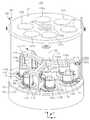
도 1 내지 도 5, 및 도 6a 내지 도 6d를 참조하면, 기판 처리 장치(100)는 진공 용기(152)에 형성된 복수의 관통홀들(111a~111f,121)에 각각 장착되는 복수의 유전체 튜브들(112a~112f,122), 상기 진공 용기(152)에 배치되는 대칭성에 따라 제1 그룹(116) 및 제2 그룹(216)으로 분류되고 상기 유전체 튜브들(112a~112f,122)의 외측에 각각 장착되는 안테나들(116a~116f,216), 상기 제1 그룹(116)의 안테나에 전력을 공급하는 제1 RF 전원(162), 상기 제2 그룹(216)의 안테나에 전력을 공급하는 제2 RF 전원(164), 및 상기 제1 그룹(116)의 안테나와 상기 제1 RF 전원(162) 사이에 배치되어 상기 제1 RF 전원(162)의 전력을 상기 제1 그룹(116)의 안테나에 전력을 분배하는 제1 전력 분배부(122)를 포함할 수 있다.1 to 5 and 6A to 6D, the
상기 진공 용기(152)는 원통 형상 또는 삭각통 형상을 가질 수 있다. 상기 진공 용기(152)는 가스를 공급하는 가스 공급부 및 가스를 배출하는 배기부를 포함할 수 있다. 상기 진공 용기(152)는 기판 홀더(154) 및 상기 기판 홀더(154)로 상에 장착되는 기판(156)을 포함할 수 있다. 상기 진공 용기(152)는 상판(153)을 포함할 수 있다. 상기 상판(153)은 상기 진공 용기(152)의 뚜껑일 수 있다. 상기 상판(153)은 금속 또는 금속 합금으로 형성될 수 있다. 상기 상판은 x-y 평면에 배치될 수 있다.The
상기 상판(153)에는 복수 개의 관통홀들(111a~111f,121)을 포함할 수 있다. 상기 관통홀들(111a~111f,121) 상에 각각 유전체 튜브들(112a~112f,122)이 배치되고, 상기 유전체 튜브들(112a~112f,122)의 진공 상태는 상기 관통홀의 상부 근처에 형성된 오링에 의하여 유지될 수 있다. 상기 유전체 튜브들(112a~112f,122)은 뚜껑이 없는 벨자(bell-jar) 형태일 수 있다. 상기 유전체 튜브들(112a~112f,122)은 와셔 형태의 지지부와 원통 형상의 실린더부를 포함할 수 있다.The
상기 유전체 튜브(112a~112f,122)는 유리, 쿼츠, 알루미나, 사파이어, 또는 세라믹으로 형성될 수 있다. 상기 유전체 튜브들(112a~112f,122)의 일단은 상기 진공 용기(152)의 관통홀에 연결되고, 상기 유전체 튜브들(112a~112f,122)의 타단은 금속 뚜껑(114a~114f,214)에 연결될 수 있다. 상기 금속 뚜껑(114a~114f,214)은 가스를 유입하기 위한 가스 유입부(115)를 포함할 수 있다. 상기 금속 뚜껑(114a~114f,214)은 헬리콘 파를 반사시켜 보강 간섭을 일으킬 수 있다. 상기 유전체 튜브(112a~112f,122)의 길이는 수 센치 미터 내지 수십 센치 미터일 수 있다. 상기 유전체 튜브(112a~112f,122)의 길이는 유전체 튜브의 반경(R), 상기 유전체 튜브에서의 자속밀도의 세기(B0), 플라즈마 밀도(n0), 및 안테나의 주파수(f)에 의하여 결정될 수 있다.The
반경이 R인 경우, 상기 유전체 튜브 내의 플라즈마가 균일하다고 가정한 경우, m=0인 헬리콘 모드에 대하여 상기 유전체 튜브(112a~112f,122)의 벽에서의 라디알 전류 밀도(radial current density)는 영이 된다. 상기 유전체 튜브(112a~112f,122)의 길이(L/2=π/kz)는 헬리콘 웨이브의 반파장에 해당되고 다음과 같이 주어진다. kz는 헬리콘 웨이브의 파수(wave number)이다.When the radius is R, assuming that the plasma in the dielectric tube is uniform, the radial current density at the walls of the

여기서, e는 전자의 전하량이고, B0는 자속 밀도의 세기이고, μ0는 투자율이이고, ω는 각주파수이고, n0은 플라즈마의 밀도이다. 주파수(f)가 13.56 Mhz이고, B0는 90 Gauss이고, n0가 4x 1012 cm-3인 경우, L은 11.3 cm일 수 있다.Where e is the charge of the electron, B0 is the intensity of the magnetic flux density, μ0 is the permeability, ω is the angular frequency, and n0 is the density of the plasma. The frequency (f) is a 13.56 Mhz, B0 is 90 Gauss and, n is0 4x 1012 cm- if the3, L may be a 11.3 cm.
안테나들(116a~116f,216)은 기하학적 대칭성을 기준으로 제1 그룹(116)과 제2 그룹(216)으로 분류될 수 있다. 제1 그룹(116)의 안테나는 동일한 구조일 수 있다. 상기 제2 그룹(216)의 안테나는 동일한 구조일 수 있다. 상기 안테나들(116a~116f,216)은 원통 형상 또는 사각통 형상의 도전성 파이프일 수 있다. 상기 안테나들(116a~116f,216)의 내부에 냉매가 흐를 수 있다.The
상기 제1 그룹의 안테나들(116a~116f)은 상기 상판(153)의 중심을 기준으로 일정한 반경의 원주의 주위에 대칭적으로 될 수 있다. 상기 제2 그룹의 안테나(216)는 상기 상판(153)의 중심에 배치될 수 있다. 상기 제1 그룹의 안테나들(116a~116f)은 6개일 수 있다. 또한, 상기 제2 그룹의 안테나(216)는 한 개일 수 있다. 상기 안테나들(116a~116f, 216)은 3 턴(turn)의 안테나일 수 있다. 상기 안테나들(116a~116f, 216)은 영구 자석들(132a~132g)과 결합하여 수 밀리 토르의 저압에서 헬리콘 플라즈마를 형성할 수 있다. 상기 진공 용기(152)의 압력이 수십 밀리토르 이상인 경우, 영구 자석들에 관계없이 유도 결합 플라즈마가 형성될 수 있다.The first group of
상기 제1 RF 전원(162)은 제1 주파수의 정현파를 출력할 수 있다. 상기 제1 RF 전원(162)의 전력은 제1 임피던스 매칭 네트워크(163)를 통하여 제1 전력 분배부(122)에 제공될 수 있다. 상기 제1 RF 전원(162)의 주파수는 수백 kHz 내지 수백 MHz 일 수 있다.The first
제1 전력 분배부(122)는 상기 제1 임피던 매칭 네트워크(163)를 통하여 공급받은 전력을 병렬 연결된 제1 그룹의 안테나들(116a~116f)에게 분배할 수 있다. 상기 제1 전력 분배부(122)는 제1 전력 분배 라인(122c), 및 상기 제1 전력 분배 라인(122c)을 감싸고 접지되는 제1 도전성 외피(122a)를 포함할 수 있다. 상기 제1 전력 분배부(122)의 입력단(N1)과 상기 제1 그룹의 안테나들(116a~116f) 사이의 거리는 동일할 수 있다. 제1 절연부는 상기 제1 전력 분배라인(122c)과 상기 제1 도전성 외피(122a) 사이에 개재될 수 있다.The
상기 제1 전력 분배부(122)는 상기 제1 RF 전원(162)으로터 전력을 공급받는 동축 케이블 형태의 입력 브랜치(123), 상기 입력 브랜치(123)와 연결되고 3 갈래로 갈라지는 동축 케이블 형태의 3 웨이(way) 브랜치(124), 및 상기 3 웨이 브랜치(124)에 연결되어 2 갈래로 갈라지는 동축 케이블 형태의 T 브랜치들(125)을 포함할 수 있다.The
상기 입력 브랜치(123)는 원통 형상일 수 있다. 상기 입력 브랜치(123)는 통축 케이블를 구조를 가지고 있다. 상기 입력 브랜치(123)는 원통형의 내부 도전체(123c), 내부 도전체를 감싸는 원통형의 절연체(123b), 및 절연체를 감싸는 원통형의 외부 도전체(123a)를 포함할 수 있다. 상기 내부 도전체(123c)에는 냉매가 흐를 수 있다.The
상기 입력 브랜치(123)의 일단은 상기 제1 임피던스 매칭 네트워크(163)에 연결되고, 상기 입력 브랜치(123)의 타단은 120도 간격으로 갈라진 상기 3 웨이(way) 브랜치(124)에 연결될 수 있다. 상기 3 웨이(way) 브랜치(124)는 축을 따라 절단된 사각통 형상일 수 있다. 상기 3 웨이(way) 브랜치(124)는 상기 상판에 z축 방향으로 이격된 xy 평면에 배치될 수 있다. 상기 3 웨이(way) 브랜치(124)는 통축 케이블 구조를 가질 수 있다. 상기 3 웨이(way) 브랜치(124)는 원통형의 내부 도전체(124c), 내부 도전체를 감싸는 절단된 사각통의 절연체(124b), 및 절연체를 감싸는 절단된 사각통 형상의 외부 도전체(124a)를 포함할 수 있다. 상기 입력 브랜치(123)의 내부 도전체(123c)를 통하여 공급된 냉매는 상기 3 웨이(way) 브랜치(124)의 내부 도전체(124c) 내부로 흐를 수 있다. One end of the
T 브랜치들(125)은 상기 3 웨이(way) 브랜치(124)에 연결되어 전력을 2 갈래로 분배할 수 있다. 상기 T 브랜치들(125)는 절단된 사각통 형상일 수 있다. 상기 T 브랜치들(125)은 통축 케이블 구조를 가질 수 있다. 상기 T 브랜치들(125)은 원통 형상의 내부 도전체(125c), 내부 도전체를 감싸는 절연체(125b), 및 절연체를 감싸는 외부 도전체(125a)를 포함할 수 있다. 상기 내부 도전체(125c) 내부로 냉매가 흐를 수 있다. 상기 T 브랜치들(125)은 동일한 길이의 팔을 가질 수 있다.The
상기 T 브랜치들(125) 각각은 한 쌍의 안테나(116a,116b)에 전력을 공급할 수 있다. 상기 T 브랜치들(125)은 동일한 형상일 수 있다. 상기 내부 도전체(125c)는 상기 안테나(116a,116b)와 연속적으로 연결되어 전력 및 냉매를 동시에 공급할 수 있다. 상기 3 웨이 브랜치(125)의 내부 도전체(125c)를 통하여 공급된 냉매는 상기 T 브랜치(125)의 내부 도전체(125c) 내부로 흐를 수 있다.Each of the
고정판들(113)은 상기 안테나들(116a~116f, 216)을 고정하고 상기 상판(153)에 고정될 수 있다. 상기 고정판들(113)의 일단은 상기 안테나들(116a~116f, 216)의 일단에 연결되어 접지될 수 있다. 상기 고정판들(113)의 타단은 접지 라인(119)의 일단에 연결되어 접지될 수 있다.The fixing
상기 접지 라인(119)은 상기 고정판(113)과 상기 T 브랜치(125)의 외부 도전체(125a)에 연결할 수 있다. 상기 접지 라인(119)의 일단은 상기 고정판(113)의 타단에 연결되고, 상기 접지 라인(119)의 타단은 상기 T 브랜치(125)의 외부 도전체(125a)에 연결될 수 있다. 상기 접지 라인(119)의 길이는 제1 그룹의 안테나들(116a~116f)에 대하여 동일할 수 있다. 이에 따라, 제1 그룹의 안테나들((116a~116f))은 모두 동일한 임피던스를 가질 수 있다.The
가스 분배부(172)는 유전체 튜브들에 가스를 공급할 수 있다. 상기 가스 분배부는 하나의 제1 전력 분배부(122)와 유사한 구조를 가지고 가스를 유전체 튜브들에 균등하게 분배할 수 있다. 상기 가스 분배부는 금속 뚜껑(214)에 형성될 수 있다. 상기 가스 분배부는 금속 투껑들(114a~114f)에 동일한 길이를 가지도록 형성될 수 있다. 구체적으로, 상기 가스 분배부(172)는 제2 그룹의 금속 투껑(214)에서 3 갈래로 분기되고, 다시 T 자로 분기되어 제1 그롭의 금속 투껑(114a~114f)에 연결될 수 있다.The
제2 RF 전원(164)은 제2 그룹(216)의 안테나에 전력을 공급할 수 있다. 상기 제1 RF 전원(162)과 제2 RF 전원(164)의 간섭을 최소화하기 위하여, 상기 제1 RF 전원(162)의 제1 주파수는 상기 제2 RF 전원(164)의 제2 주파수와 서로 다를 수 있다. 예를 들어, 상기 제1 주파수는 13.56 Mhz이고, 제2 주파수는 12Mhz일 수 있다.The second
상기 제2 RF 전원(164)은 제2 임피던스 매칭 네트워크(165)를 통하여 제2 그룹의 안테나(216)에 직접 연결될 수 있다.The second
영구자석(132a~132g)은 도넛 형상 또는 토로이드 형상일 수 있다. 상기 영구 자석(132a~132g)의 단면은 사각형 또는 원형일 수 있다. 상기 영구 자석의 자화 방향은 상기 영구 자석이 배치된 평면에 수직할 수 있다.Permanent magnets (132a ~ 132g) may be a donut shape or toroidal shape. Cross sections of the
상기 영구 자석(132a~132g)은 영구 자석 고정판(141)에 삽입될 수 있다. 상기 영구 자석은 상기 안테나의 중심에서 z 축 방향으로 이격되어 배치될 수 있다.The
이동부(140)는 상기 상판(153)에 고정 결합할 수 있다. 상기 이동부(140)는 상기 유전체 튜브들이 배치된 평면(xy 평면)에 수직하게 연장되는 적어도 하나의 지지 기둥(142)을 포함할 수 있다. 상기 영구 자석 고정판(141)은 상기 지지 기둥(142)에 삽입되어 상기 지지 기둥(142)을 따라 이동할 수 있다. 상기 영구 자석 고정판(141)의 중심에는 관통홀(143)이 배치될 수 있다. 상기 입력 브랜치(123)는 상기 관통홀(143)을 관통하여 상기 제1 임피던스 매칭 네트워크(163)에 연결될 수 있다.The moving
상기 영구 자석 고정판(141)은 상기 영구 자석(132a~132g)을 고정하는 수단일 수 있다. 상기 영구 자석(132a~132g)은 상기 안테나들에 z축 방향으로 정렬되어 배치될 수 있다. 상기 영구 자석(132a~132g)은 상기 영구 자석 고정판(141)에 삽입되어 고정될 수 있다. 상기 이동부(140)는 유전체 튜브에서의 자속 밀도(B0)의 세기를 조절하여 헬리콘 모드를 발생시킬 수 있다. 예를 들어, 주어진 조건(L, ω, R)에 대하여, 자속 밀도(B0)에 대한 플라즈마 밀도(n0)의 비(B0/n0)이 일정하도록 이동부(140)는 이동할 수 있다. 이에 따라, 균일한 플라즈마가 생성될 수 있다.The permanent
도 7은 본 발명의 다른 실시예에 따른 플라즈마 발생 장치를 설명하는 평면도이다.7 is a plan view illustrating a plasma generating apparatus according to another embodiment of the present invention.
도 8은 도 7의 플라즈마 발생 장치의 회로도이다.FIG. 8 is a circuit diagram of the plasma generator of FIG. 7.
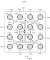
도 7 및 도 8을 참조하면, 플라즈마 발생 장치(400)는 진공 용기(453)에 형성된 복수의 관통홀들에 각각 장착되는 복수의 유전체 튜브들(312a~312l, 412a~412d), 상기 진공 용기(453)에 배치되는 대칭성에 따라 제1 그룹(316) 및 제2 그룹(416)으로 분류되고 상기 유전체 튜브들(312a~312l,412a~412d)의 외측에 각각 장착되는 안테나들(316a~316l, 416a~416d), 상기 제1 그룹(316)의 안테나에 전력을 공급하는 제1 RF 전원(162), 상기 제2 그룹(416)의 안테나에 전력을 공급하는 제2 RF 전원(164), 및 상기 제1 그룹(316)의 안테나와 상기 제1 RF 전원(162) 사이에 배치되어 상기 제1 RF 전원(162)의 전력을 상기 제1 그룹(316)의 안테나에 전력을 분배하는 제1 전력 분배부(322)를 포함한다.7 and 8, the
상기 안테나들(316a~316l,416a~416d)은 상기 진공 용기(453)의 사각형의 상판에 4 x 4 매트릭스 형태로 배치될 수 있다. 상기 제1 그룹(316)의 안테나는 외곽을 따라 배치될 수 있다. 상기 제2 그룹(416)의 안테나는 상기 제1 그룹(316)의 안테나로 둘러싸이도록 내측에 배치될 수 있다.The
상기 제1 전력 분배부(322)는 제1 전력 분배 라인(322c), 및 상기 제1 전력 분배 라인을 감싸고 접지되는 제1 도전성 외피(322a)를 포함할 수 있다. 상기 제1 전력 분배부(322)의 입력단(N1)과 상기 제1 그룹(316)의 안테나 사이의 거리는 동일할 수 있다.The first
상기 제2 전력 분배부(422)는 상기 제2 RF 전원(164)과 상기 제2 그룹(416)의 안테나 사이에 배치될 수 있다. 상기 제2 전력 분배부(422)는 제2 전력 분배 라인(422c), 및 상기 제2 전력 분배 라인을 감싸고 접지되는 제2 도전성 외피(422a)를 포함할 수 있다. 상기 제2 전력 분배부(422)의 입력단(N2)과 상기 제2 그룹(416)의 안테나 사이의 거리는 동일할 수 있다.The
상기 안테나들(316a~316l,416a~416d)은 접지 라인을 통하여 상기 진공 용기(453)에 접지될 수 있다.The
영구 자석은 상기 안테나들(316a~316l,416a~416d) 상에 배치될 수 있다. 이동부는 상기 영구 자석과 상기 안테나들(316a~316l,416a~416d) 사이의 거리를 조절할 수 있다.Permanent magnets may be disposed on the
도 9는 본 발명의 또 다른 실시예에 따른 플라즈마 발생 장치를 설명하는 도면이다. 도 1에서 설명한 것과 중복되는 설명은 생략한다.9 is a view for explaining a plasma generating apparatus according to another embodiment of the present invention. Descriptions overlapping with those described in FIG. 1 will be omitted.
도 9를 참조하면, 플라즈마 발생 장치(100a)는 진공 용기(152)에 형성된 복수의 관통홀들(111a~111f,121)에 각각 장착되는 복수의 유전체 튜브들(112a~112f,122), 상기 진공 용기(152)에 배치되는 대칭성에 따라 제1 그룹(116) 및 제2 그룹(216)으로 분류되고 상기 유전체 튜브들(112a~112f,122)의 외측에 각각 장착되는 안테나들(116a~116f,216), 상기 제1 그룹(116)의 안테나에 전력을 공급하는 제1 RF 전원(162), 상기 제2 그룹(216)의 안테나에 전력을 공급하는 제2 RF 전원(164), 및 상기 제1 그룹(116)의 안테나와 상기 제1 RF 전원(162) 사이에 배치되어 상기 제1 RF 전원(162)의 전력을 상기 제1 그룹(116)의 안테나에 전력을 분배하는 제1 전력 분배부(122)를 포함할 수 있다.Referring to FIG. 9, the
가스 분배부(172)는 유전체 튜브들에 가스를 공급할 수 있다. 상기 가스 분배부는 금속 뚜껑(214)에 형성될 수 있다. 상기 가스 분배부는 제1 그룹의 안테나들(116a~116f)이 설치된 유전체 튜브들(112a~112f)에 상기 동일한 길이를 가지도록 형성될 수 있다.The
영구 자석들은 제1 그룹의 안테나에 대응하는 제1 그룹의 영구 자석과 제2 그룹의 안테나에 대응하는 제2 그룹의 영구 자석으로 분류될 수 있다. 이동부는 제1 이동부 및 제2 이동부를 포함할 수 있다. 제1 이동부는 제1 지지 기둥과 제1 그룹의 영구자석을 고정하는 제1 영구 자석 고정판을 포함할 수 있다. 제1 영구 자석 고정판은 상기 제1 지지 기둥을 따라 z축으로 이동할 수 있다. 제2 이동부는 제2 지지 기둥과 제2 그룹의 영구 자석을 고정하는 제2 영구 자석 고정판을 포함할 수 있다. 제2 영구 자석 고정판은 상기 제2 지지 기둥에 따라 z축으로 이동할 수 있다.The permanent magnets may be classified into a first group of permanent magnets corresponding to the first group of antennas and a second group of permanent magnets corresponding to the second group of antennas. The moving part may include a first moving part and a second moving part. The first moving part may include a first permanent magnet fixing plate that fixes the first support pillar and the first group of permanent magnets. The first permanent magnet fixing plate may move in the z axis along the first support pillar. The second moving part may include a second permanent magnet fixing plate that fixes the second support pillar and the second group of permanent magnets. The second permanent magnet fixing plate may move in the z axis along the second supporting column.
그리드(Grid)들이 각각 상기 관통홀의 하부에 배치될 수 있다. 상기 그리드들은 도전성 물질로 형성될 수 있다. 이에 따라, 유전체 튜브 내에서 방전된 플라즈마는 상기 유전체 튜브 내부에 한정될 수 있다. 이에 따라, 기판은 플라즈마에 직접 노출되지 않고 처리될 수 있다.Grids may be disposed below the through holes, respectively. The grids may be formed of a conductive material. Accordingly, the plasma discharged in the dielectric tube may be confined within the dielectric tube. Thus, the substrate can be processed without being directly exposed to the plasma.
이상에서는 본 발명을 특정의 바람직한 실시예에 대하여 도시하고 설명하였으나, 본 발명은 이러한 실시예에 한정되지 않으며, 당해 발명이 속하는 기술분야에서 통상의 지식을 가진 자가 특허청구범위에서 청구하는 본 발명의 기술적 사상을 벗어나지 않는 범위 내에서 실시할 수 있는 다양한 형태의 실시예들을 모두 포함한다.While the invention has been shown and described with respect to certain preferred embodiments thereof, the invention is not limited to these embodiments, and has been claimed by those of ordinary skill in the art to which the invention pertains. It includes all the various forms of embodiments that can be implemented without departing from the spirit.
100: 플라즈마 발생 장치
152: 진공 용기
111a~111f,121: 관통홀들
112a~112f,122: 유전체 튜브들
116: 제1 그룹
216: 제2 그룹
162: 제1 RF 전원
122: 제1 전력 분배부
164: 제2 RF 전원100: Plasma generator
152: vacuum container
111a-111f, 121: through holes
112a-112f, 122: dielectric tubes
116: first group
216: second group
162: first RF power supply
122: first power distribution unit
164: second RF power supply
Claims (15)
Translated fromKorean상기 진공 용기에 배치되는 대칭성에 따라 제1 그룹 및 제2 그룹으로 분류되고 상기 유전체 튜브들의 외측에 각각 장착되는 안테나들;
상기 제1 그룹의 안테나에 전력을 공급하는 제1 RF 전원;
상기 제2 그룹의 안테나에 전력을 공급하는 제2 RF 전원; 및
상기 제1 그룹의 안테나와 상기 제1 RF 전원 사이에 배치되어 상기 제1 RF 전원의 전력을 상기 제1 그룹의 안테나에 분배하는 제1 전력 분배부를 포함하고,
상기 제1 그룹의 안테나들은 상기 진공 용기의 상판의 중심을 기준으로 일정한 반경의 원주의 주위에 대칭적으로 되고,
상기 제2 그룹의 안테나는 상기 상판의 중심에 배치되고,
상기 제1 전력 분배부는:
제1 전력 분배 라인; 및
상기 제1 전력 분배 라인을 감싸고 접지되는 제1 도전성 외피를 포함하고,
상기 제1 그룹의 안테나의 일단은 상기 제1 전력 분배라인의 일단에 연결되고, 상기 제1 그룹의 안테나의 타단은 상기 제1 도전성 외피의 일단에 연결되는 것을 특징으로 하는 플라즈마 발생 장치.A plurality of dielectric tubes each mounted in a plurality of through holes formed in the vacuum container;
Antennas, each classified into a first group and a second group according to symmetry disposed in the vacuum container, and mounted to the outside of the dielectric tubes;
A first RF power source for supplying power to said first group of antennas;
A second RF power source for powering the second group of antennas; And
A first power distribution unit disposed between the first group of antennas and the first RF power source to distribute power of the first RF power source to the first group of antennas,
The first group of antennas are symmetrical around a circumference of a constant radius relative to the center of the top plate of the vacuum vessel,
The second group of antennas is disposed in the center of the top plate,
The first power distribution unit:
A first power distribution line; And
A first conductive envelope surrounding and grounding the first power distribution line,
One end of the antenna of the first group is connected to one end of the first power distribution line, and the other end of the antenna of the first group is connected to one end of the first conductive shell.
상기 제1 전력 분배부의 입력단과 상기 제1 그룹의 안테나 사이의 거리는 동일한 것을 특징으로 하는 플라즈마 발생 장치.The method according to claim 1,
And a distance between an input terminal of the first power distributor and an antenna of the first group is the same.
상기 제2 RF 전원과 상기 제2 그룹의 안테나 사이에 배치되는 상기 제2 전력 분배부를 더 포함하고,
상기 제2 전력 분배부는:
제2 전력 분배 라인; 및
상기 제2 전력 분배 라인을 감싸고 접지되는 제2 도전성 외피를 포함하고,
상기 제2 전력 분배부의 입력단과 상기 제2 그룹의 안테나 사이의 거리는 동일한 것을 특징으로 하는 플라즈마 발생 장치.The method according to claim 1,
The second power distribution unit is disposed between the second RF power source and the second group of antennas.
The second power distribution unit:
A second power distribution line; And
A second conductive shell surrounding and grounding the second power distribution line,
And a distance between an input terminal of the second power distributor and an antenna of the second group is the same.
상기 유전체 튜브들의 길이 방향으로 이격되어 배치되는 토로이드 형태의 영구 자석들을 더 포함하는 것을 특징으로 하는 플라즈마 발생 장치.The method according to claim 1,
Plasma generator further comprises a toroidal permanent magnets disposed spaced apart in the longitudinal direction of the dielectric tubes.
상기 영구 자석들의 전부 또는 일부를 고정하고 상기 영구 자석들이 배치되는 평면을 이동시키는 이동부를 더 포함하고,
상기 이동부는 주어진 조건(L,ω,R)에 대하여, 자속밀도(B0)에 대한 플라즈마 밀도(n0)의 비(B0/n0)가 일정하도록 이동시키고,
B0는 상기 유전체 튜브들의 중심에서 자속 밀도의 세기이고, R은 유전체 튜브의 반경이고, 유전체 튜브의 길이는 L/2이고, ω는 상기 제1 RF 전원의 각주파수이고, n0은 플라즈마의 밀도인 것을 특징으로 하는 플라즈마 발생 장치.5. The method of claim 4,
A moving part which fixes all or some of the permanent magnets and moves a plane in which the permanent magnets are disposed;
The moving unit moves the ratio (B0 / n0 ) of the plasma density (n0 ) to the magnetic flux density (B0 ) for a given condition (L, ω, R),
B0 is the intensity of the magnetic flux density in the center of the dielectric tubes, R is the radius of the dielectric tube, the length of the dielectric tube is L / 2, ω is the angular frequency of the first RF power source, n0 is the plasma Plasma generator, characterized in that the density.
상기 이동부는:
상기 진공 용기에 고정 결합하고 상기 유전체 튜브들이 배치된 평면에 수직하게 연장되는 적어도 하나의 지지 기둥; 및
상기 영구 자석들이 장착되고 상기 지지 기둥에 삽입되어 상기 지지 기둥을 따라 이동 가능한 영구 자석 고정판을 포함하는 것을 특징으로 하는 플라즈마 발생 장치.6. The method of claim 5,
The moving part:
At least one support pillar fixedly coupled to the vacuum vessel and extending perpendicular to a plane in which the dielectric tubes are disposed; And
And a permanent magnet fixing plate mounted with the permanent magnets and inserted into the support pillar and movable along the support pillar.
상기 유전체 튜브들의 일단에 각각 장착되는 금속 뚜껑들; 및
상기 유전체 튜브들에 가스를 공급하는 가스 분배부를 더 포함하고,
상기 가스 분배부는 상기 원주의 주위에 대칭적으로 배치되는 상기 유전체 튜브들에 동일한 길이를 가지는 것을 특징으로 하는 플라즈마 발생 장치.The method according to claim 1,
Metal lids mounted to one end of the dielectric tubes, respectively; And
Further comprising a gas distribution for supplying gas to the dielectric tubes,
And the gas distribution part has the same length to the dielectric tubes disposed symmetrically around the circumference.
상기 제1 전력 분배부는:
상기 제1 RF 전원으로터 전력을 공급받는 동축 케이블 형태의 입력 브랜치;
상기 입력 브랜치와 연결되고 3 갈래로 갈라지는 동축 케이블 형태의 3 웨이(way) 브랜치; 및
상기 3 웨이 브랜치에 연결되어 2 갈래로 갈라지는 동축 케이블 형태의 T 브랜치들을 포함하는 것을 특징으로 하는 플라즈마 발생 장치.The method according to claim 1,
The first power distribution unit:
An input branch in the form of a coaxial cable receiving power from the first RF power source;
A three-way branch in the form of a coaxial cable connected to the input branch and split into three branches; And
And three T-branches in the form of coaxial cables connected to the three-way branch.
상기 안테나들을 고정하고 상기 상판에 고정되는 고정판들; 및
상기 고정판과 상기 T 브랜치들의 외측 도선을 연결하는 접지 라인을 더 포함하고,
상기 고정판들의 일단은 상기 안테나들을 통하여 상기 T 브랜치들의 내측 도선에 연결되고, 상기 고정판들의 타단은 상기 접지 라인에 연결되고,
상기 접지 라인의 길이는 모든 안테나들에 대하여 동일한 것을 특징으로 하는 플라즈마 발생 장치.The method of claim 8,
Fixing plates fixing the antennas and fixed to the upper plate; And
And a ground line connecting the fixing plate and the outer conductorof the T branches,
One end of the fixing plates is connected to the inner lead of the T branches via the antennas, the other end of the fixing plates is connected to the ground line,
And the length of the ground line is the same for all antennas.
상기 유전체 튜브들의 일단에 각각 장착되는 금속 뚜껑들을 더 포함하고,
상기 유전체 튜브들의 길이(L/2=π/kz)은

조건을 만족하고,
R은 상기 유전체 튜브들의 반경이고,
B0는 상기 유전체 튜브들의 중심에서 자속 밀도의 세기이고, μ0는 투자율이이고, ω는 상기 제1 RF 전원의 각주파수이고, n0은 플라즈마의 밀도이고,
kz는 헬리콘 웨이브의 파수(wave number)이고,
상기 유전체 튜브들의 길이는 L/2 이고,
e는 전자의 전하량인 것을 특징으로 하는 플라즈마 발생 장치.The method according to claim 1,
Further comprising metal lids each mounted to one end of said dielectric tubes,
The length of the dielectric tubes (L / 2 = π / kz ) is
Satisfy the conditions,
R is the radius of the dielectric tubes,
B0 is the intensity of magnetic flux density at the center of the dielectric tubes, μ0 is the permeability, ω is the angular frequency of the first RF power source, n0 is the density of the plasma,
kz is the wave number of the helicon wave,
The length of the dielectric tubes is L / 2,
e is a charge amount of electrons.
상기 제1 RF 전원의 구동 주파수는 상기 제2 RF 전원의 구동 주파수와 서로 다른 것을 특징으로 하는 플라즈마 발생 장치.The method according to claim 1,
And a driving frequency of the first RF power supply is different from a driving frequency of the second RF power supply.
상기 입력 브렌치는 원통 형상이고, 상기 3 웨이 브랜치는 사각형 형상이고, 상기 T 브랜치는 사각형 형상이고,
상기 제1 전력 분배 라인은 파이프 형상이고, 그 내부에 냉매가 흐르고, 상기 냉매는 상기 제1 룹의 안테나들에 제공되는 것을 특징으로 하는 플라즈마 발생장치.The method of claim 8,
The input branch is cylindrical, the three-way branch is rectangular, the T branch is rectangular,
And the first power distribution line has a pipe shape, a refrigerant flows therein, and the refrigerant is provided to the antennas of the first group.
상기 진공 용기에 배치되는 대칭성에 따라 제1 그룹 및 제2 그룹으로 분류되고 상기 유전체 튜브들의 외측에 각각 장착되는 안테나들;
상기 제1 그룹의 안테나에 전력을 공급하는 제1 RF 전원;
상기 제2 그룹의 안테나에 전력을 공급하는 제2 RF 전원; 및
상기 제1 그룹의 안테나와 상기 제1 RF 전원 사이에 배치되어 상기 제1 RF 전원의 전력을 상기 제1 그룹의 안테나에 분배하는 제1 전력 분배부를 포함하고,
상기 안테나들은 상기 진공 용기의 사각형의 상판에 매트릭스 형태로 배치되고,
상기 제1 그룹의 안테나는 외곽을 따라 배치되고,
상기 제2 그룹의 안테나는 상기 제1 그룹의 안테나로 둘러싸이도록 내측에 배치되고,
상기 제1 전력 분배부는:
제1 전력 분배 라인; 및
상기 제1 전력 분배 라인을 감싸고 접지되는 제1 도전성 외피를 포함하고,
상기 제1 그룹의 안테나의 일단은 상기 제1 전력 분배라인의 일단에 연결되고, 상기 제1 그룹의 안테나의 타단은 상기 제1 도전성 외피의 일단에 연결되는 것을 특징으로 하는 플라즈마 발생 장치.A plurality of dielectric tubes each mounted in a plurality of through holes formed in the vacuum container;
Antennas, each classified into a first group and a second group according to symmetry disposed in the vacuum container, and mounted to the outside of the dielectric tubes;
A first RF power source for supplying power to said first group of antennas;
A second RF power source for powering the second group of antennas; And
A first power distributor disposed between the first group of antennas and the first RF power source to distribute power of the first RF power source to the first group of antennas,
The antennas are arranged in a matrix form on the rectangular top plate of the vacuum vessel,
The antenna of the first group is disposed along the outer edge,
The antenna of the second group is disposed inside to be surrounded by the antenna of the first group,
The first power distribution unit:
A first power distribution line; And
A first conductive envelope surrounding and grounding the first power distribution line,
One end of the antenna of the first group is connected to one end of the first power distribution line, and the other end of the antenna of the first group is connected to one end of the first conductive shell.
상기 제2 그룹의 안테나와 상기 제2 RF 전원 사이에 배치되어, 상기 제2 RF 전원의 전력은 상기 제2 그룹의 안테나에 분배하는 제2 전력 분배부를 더 포함하는 것을 특징으로 하는 플라즈마 발생장치.The method of claim 13,
And a second power distribution unit disposed between the second group of antennas and the second RF power source, wherein the power of the second RF power source is distributed to the antennas of the second group.
상기 관통홀들의 하부에 배치된 그리드들을 더 포함하는 것을 특징으로 하는 플라즈마 발생장치.The method according to claim 1 or 13,
And a grid disposed under the through holes.
Priority Applications (4)
| Application Number | Priority Date | Filing Date | Title |
|---|---|---|---|
| KR1020110104792AKR101246191B1 (en) | 2011-10-13 | 2011-10-13 | Plasma generation apparatus and substrate processing apparatus |
| PCT/KR2012/007977WO2013055056A1 (en) | 2011-10-13 | 2012-10-02 | Plasma apparatus and substrate-processing apparatus |
| CN201280047361.0ACN103843465B (en) | 2011-10-13 | 2012-10-02 | Plasma device and substrate processing device |
| US14/251,013US9734990B2 (en) | 2011-10-13 | 2014-04-11 | Plasma apparatus and substrate-processing apparatus |
Applications Claiming Priority (1)
| Application Number | Priority Date | Filing Date | Title |
|---|---|---|---|
| KR1020110104792AKR101246191B1 (en) | 2011-10-13 | 2011-10-13 | Plasma generation apparatus and substrate processing apparatus |
Related Child Applications (1)
| Application Number | Title | Priority Date | Filing Date |
|---|---|---|---|
| KR1020120145015ADivisionKR101735296B1 (en) | 2012-12-13 | 2012-12-13 | Plasma generation apparatus and substrate processing apparatus |
Publications (1)
| Publication Number | Publication Date |
|---|---|
| KR101246191B1true KR101246191B1 (en) | 2013-03-21 |
Family
ID=48082068
Family Applications (1)
| Application Number | Title | Priority Date | Filing Date |
|---|---|---|---|
| KR1020110104792AActiveKR101246191B1 (en) | 2011-10-13 | 2011-10-13 | Plasma generation apparatus and substrate processing apparatus |
Country Status (4)
| Country | Link |
|---|---|
| US (1) | US9734990B2 (en) |
| KR (1) | KR101246191B1 (en) |
| CN (1) | CN103843465B (en) |
| WO (1) | WO2013055056A1 (en) |
Cited By (8)
| Publication number | Priority date | Publication date | Assignee | Title |
|---|---|---|---|---|
| KR20140120405A (en)* | 2013-04-02 | 2014-10-14 | 주식회사 윈텔 | Gate Dielectric Layer Forming Method |
| WO2015194794A1 (en)* | 2014-06-16 | 2015-12-23 | 주식회사 윈텔 | Plasma generation device |
| KR20190077282A (en)* | 2019-06-24 | 2019-07-03 | 윈텔코퍼레이션 주식회사 | Plasma Generation Apparatus |
| WO2021061463A1 (en)* | 2019-09-27 | 2021-04-01 | Applied Materials, Inc. | Monolithic modular microwave source with integrated temperature control |
| WO2021061487A1 (en)* | 2019-09-27 | 2021-04-01 | Applied Materials, Inc. | Monolithic modular microwave source with integrated process gas distribution |
| WO2021061513A1 (en)* | 2019-09-27 | 2021-04-01 | Applied Materials, Inc. | Modular microwave source with embedded ground surface |
| US12300497B2 (en) | 2021-02-11 | 2025-05-13 | Applied Materials, Inc. | Method and apparatus of low temperature plasma enhanced chemical vapor deposition of graphene |
| US12424422B2 (en) | 2021-12-29 | 2025-09-23 | Samsung Electronics Co., Ltd. | Plasma processing apparatus and semiconductor device manufacturing method |
Families Citing this family (14)
| Publication number | Priority date | Publication date | Assignee | Title |
|---|---|---|---|---|
| KR101241049B1 (en) | 2011-08-01 | 2013-03-15 | 주식회사 플라즈마트 | Plasma generation apparatus and plasma generation method |
| KR101246191B1 (en) | 2011-10-13 | 2013-03-21 | 주식회사 윈텔 | Plasma generation apparatus and substrate processing apparatus |
| KR101332337B1 (en) | 2012-06-29 | 2013-11-22 | 태원전기산업 (주) | Microwave lighting lamp apparatus |
| KR20140087215A (en)* | 2012-12-28 | 2014-07-09 | 주식회사 윈텔 | Plasma generation apparatus and substrate processing apparatus |
| KR101533032B1 (en)* | 2015-02-03 | 2015-07-01 | 성균관대학교산학협력단 | Thin film depositing apparatus |
| US20170092470A1 (en)* | 2015-09-28 | 2017-03-30 | Applied Materials, Inc. | Plasma reactor for processing a workpiece with an array of plasma point sources |
| CN107333378B (en)* | 2016-04-29 | 2019-05-03 | 中微半导体设备(上海)股份有限公司 | A kind of device for inductively coupled plasma processing and its control method |
| US20180174801A1 (en)* | 2016-12-21 | 2018-06-21 | Ulvac Technologies, Inc. | Apparatuses and methods for surface treatment |
| KR101880747B1 (en)* | 2017-08-30 | 2018-07-20 | 주식회사 말타니 | Microwave Discharge Lamp |
| KR102479923B1 (en)* | 2018-08-22 | 2022-12-20 | 어플라이드 머티어리얼스, 인코포레이티드 | High Density Plasma Enhanced Chemical Vapor Deposition Chamber |
| US11094508B2 (en)* | 2018-12-14 | 2021-08-17 | Applied Materials, Inc. | Film stress control for plasma enhanced chemical vapor deposition |
| JP7221115B2 (en)* | 2019-04-03 | 2023-02-13 | 東京エレクトロン株式会社 | Plasma processing method and plasma processing apparatus |
| CN113889391B (en)* | 2020-07-02 | 2024-03-12 | 中微半导体设备(上海)股份有限公司 | Plasma processing apparatus and insulating window assembly thereof |
| CN111779647B (en)* | 2020-07-17 | 2022-04-01 | 上海空间推进研究所 | Multi-discharge-channel helicon wave plasma thruster suitable for space application |
Citations (3)
| Publication number | Priority date | Publication date | Assignee | Title |
|---|---|---|---|---|
| JP2000277506A (en)* | 1999-03-24 | 2000-10-06 | Sanyo Electric Co Ltd | Plasma cvd system and film-forming method |
| KR20050110548A (en)* | 2004-05-19 | 2005-11-23 | 정규선 | Triple plasma generator for simulation and diagnostics of semiconductor processing, nuclear fusion and space plasmas |
| KR20090005542A (en)* | 2007-07-09 | 2009-01-14 | 엘지전자 주식회사 | Power distributor for high frequency plasma generator and its manufacturing method |
Family Cites Families (107)
| Publication number | Priority date | Publication date | Assignee | Title |
|---|---|---|---|---|
| US3979624A (en) | 1975-04-29 | 1976-09-07 | Westinghouse Electric Corporation | High-efficiency discharge lamp which incorporates a small molar excess of alkali metal halide as compared to scandium halide |
| US5114770A (en)* | 1989-06-28 | 1992-05-19 | Canon Kabushiki Kaisha | Method for continuously forming functional deposited films with a large area by a microwave plasma cvd method |
| US5404076A (en) | 1990-10-25 | 1995-04-04 | Fusion Systems Corporation | Lamp including sulfur |
| AU3977193A (en) | 1990-10-25 | 1993-11-18 | Fusion Systems Corporation | Lamp having controllable characteristics |
| ES2101759T3 (en) | 1990-10-25 | 1997-07-16 | Fusion Systems Corp | HIGH POWER LAMP. |
| US5330578A (en) | 1991-03-12 | 1994-07-19 | Semiconductor Energy Laboratory Co., Ltd. | Plasma treatment apparatus |
| US6074512A (en)* | 1991-06-27 | 2000-06-13 | Applied Materials, Inc. | Inductively coupled RF plasma reactor having an overhead solenoidal antenna and modular confinement magnet liners |
| US5479072A (en) | 1991-11-12 | 1995-12-26 | General Electric Company | Low mercury arc discharge lamp containing neodymium |
| US5227698A (en) | 1992-03-12 | 1993-07-13 | Fusion Systems Corporation | Microwave lamp with rotating field |
| DE69329032T2 (en) | 1992-09-30 | 2001-03-22 | Fusion Lighting Inc., Rockville | ELECTRODELESS LAMP WITH ROTATING BULB |
| JP3350973B2 (en) | 1992-10-12 | 2002-11-25 | 松下電器産業株式会社 | Plasma processing method and plasma processing apparatus |
| BR9407816A (en) | 1993-10-15 | 1997-05-06 | Fusion Lighting Inc | Electrode-free lamp with improved performance |
| US5556549A (en) | 1994-05-02 | 1996-09-17 | Lsi Logic Corporation | Power control and delivery in plasma processing equipment |
| AU2003195A (en) | 1994-06-21 | 1996-01-04 | Boc Group, Inc., The | Improved power distribution for multiple electrode plasma systems using quarter wavelength transmission lines |
| US5811022A (en)* | 1994-11-15 | 1998-09-22 | Mattson Technology, Inc. | Inductive plasma reactor |
| US5594303A (en) | 1995-03-09 | 1997-01-14 | Fusion Lighting, Inc. | Apparatus for exciting an electrodeless lamp with an increasing electric field intensity |
| IL117972A (en) | 1995-04-21 | 1999-06-20 | Fusion Lighting Inc | Compact microwave lamp |
| US6042686A (en) | 1995-06-30 | 2000-03-28 | Lam Research Corporation | Power segmented electrode |
| US5653811A (en)* | 1995-07-19 | 1997-08-05 | Chan; Chung | System for the plasma treatment of large area substrates |
| US5565074A (en) | 1995-07-27 | 1996-10-15 | Applied Materials, Inc. | Plasma reactor with a segmented balanced electrode for sputtering process materials from a target surface |
| JP3951003B2 (en) | 1995-11-17 | 2007-08-01 | 俊夫 後藤 | Plasma processing apparatus and method |
| US5688064A (en) | 1996-10-30 | 1997-11-18 | Fusion Lighting, Inc. | Method and apparatus for coupling bulb stem to rotatable motor shaft |
| AU1078097A (en) | 1996-01-26 | 1997-08-20 | Fusion Lighting, Inc. | Method and apparatus for coupling bulb stem to rotatable motor shaft |
| US5846883A (en) | 1996-07-10 | 1998-12-08 | Cvc, Inc. | Method for multi-zone high-density inductively-coupled plasma generation |
| KR100505176B1 (en) | 1996-09-27 | 2005-10-10 | 서페이스 테크놀로지 시스템스 피엘씨 | Plasma Processing Equipment |
| TW406280B (en) | 1997-05-21 | 2000-09-21 | Fusion Lighting Inc | non-rotating electrodeless lamp containing molecular fill |
| SE511139C2 (en)* | 1997-11-20 | 1999-08-09 | Hana Barankova | Plasma processing apparatus with rotatable magnets |
| US6352049B1 (en) | 1998-02-09 | 2002-03-05 | Applied Materials, Inc. | Plasma assisted processing chamber with separate control of species density |
| US6049086A (en) | 1998-02-12 | 2000-04-11 | Quester Technology, Inc. | Large area silent discharge excitation radiator |
| US6189484B1 (en)* | 1999-03-05 | 2001-02-20 | Applied Materials Inc. | Plasma reactor having a helicon wave high density plasma source |
| JP3332857B2 (en) | 1998-04-15 | 2002-10-07 | 三菱重工業株式会社 | High frequency plasma generator and power supply method |
| US20010002584A1 (en)* | 1998-12-01 | 2001-06-07 | Wei Liu | Enhanced plasma mode and system for plasma immersion ion implantation |
| JP2000277599A (en) | 1999-03-25 | 2000-10-06 | Ibiden Co Ltd | Electrostatic chuck |
| JP4601104B2 (en) | 1999-12-20 | 2010-12-22 | キヤノンアネルバ株式会社 | Plasma processing equipment |
| TW462207B (en) | 2000-02-24 | 2001-11-01 | Nano Architect Res Corp | Method and apparatus for generating high-density uniform plasma by inductively coupling |
| JP4718093B2 (en) | 2000-03-28 | 2011-07-06 | 東京エレクトロン株式会社 | Method and system for controlling power supplied to a composite segment electrode |
| KR100323613B1 (en) | 2000-03-29 | 2002-02-19 | 박세근 | Apparatus for generating a large area plasma source |
| US6451161B1 (en)* | 2000-04-10 | 2002-09-17 | Nano-Architect Research Corporation | Method and apparatus for generating high-density uniform plasma |
| US6685798B1 (en)* | 2000-07-06 | 2004-02-03 | Applied Materials, Inc | Plasma reactor having a symmetrical parallel conductor coil antenna |
| JP2002025919A (en) | 2000-07-12 | 2002-01-25 | Sharp Corp | Capacitively coupled plasma apparatus and method for manufacturing electronic device |
| TWI239794B (en) | 2002-01-30 | 2005-09-11 | Alps Electric Co Ltd | Plasma processing apparatus and method |
| TWI283899B (en) | 2002-07-09 | 2007-07-11 | Applied Materials Inc | Capacitively coupled plasma reactor with magnetic plasma control |
| US20030015965A1 (en)* | 2002-08-15 | 2003-01-23 | Valery Godyak | Inductively coupled plasma reactor |
| CA2471987C (en) | 2002-10-07 | 2008-09-02 | Sekisui Chemical Co., Ltd. | Plasma surface processing apparatus |
| KR100494999B1 (en) | 2002-10-15 | 2005-06-16 | 태원전기산업 (주) | Apparatus To Generate A Rotating Field For Electrodeless High-intensity Discharge Lamps |
| CN1293608C (en) | 2002-10-16 | 2007-01-03 | 夏普株式会社 | Semiconductor device and its manufacturing method and plasma processing device |
| KR100615015B1 (en) | 2002-10-16 | 2006-08-25 | 샤프 가부시키가이샤 | Electronic device, production method thereof, and plasma process apparatus |
| AU2002344594B2 (en) | 2002-10-29 | 2005-06-09 | Mitsubishi Heavy Industries, Ltd. | Method and device for generating uniform high-frequency plasma over large surface area used for plasma chemical vapor deposition apparatus |
| US8835869B2 (en)* | 2003-02-04 | 2014-09-16 | Veeco Instruments, Inc. | Ion sources and methods for generating an ion beam with controllable ion current density distribution |
| US7183716B2 (en)* | 2003-02-04 | 2007-02-27 | Veeco Instruments, Inc. | Charged particle source and operation thereof |
| KR100522995B1 (en) | 2003-06-02 | 2005-10-24 | 태원전기산업 (주) | Non-Rotating Electrodeless High-Intensity Discharge Lamp System Using Circularly Polarized Microwaves |
| US7273533B2 (en)* | 2003-11-19 | 2007-09-25 | Tokyo Electron Limited | Plasma processing system with locally-efficient inductive plasma coupling |
| US20070119828A1 (en) | 2003-12-08 | 2007-05-31 | Ngk Insulators , Ltd. | Plasma generating electrode, its manufacturing method, and plasma reactor |
| JP3816081B2 (en) | 2004-03-10 | 2006-08-30 | 松下電器産業株式会社 | Plasma etching apparatus and plasma etching method |
| KR100576093B1 (en) | 2004-03-15 | 2006-05-03 | 주식회사 뉴파워 프라즈마 | Plasma reaction chamber with multiple arrayed vacuum chambers |
| US7767561B2 (en)* | 2004-07-20 | 2010-08-03 | Applied Materials, Inc. | Plasma immersion ion implantation reactor having an ion shower grid |
| US7163877B2 (en)* | 2004-08-18 | 2007-01-16 | Tokyo Electron Limited | Method and system for modifying a gate dielectric stack containing a high-k layer using plasma processing |
| JPWO2006118161A1 (en) | 2005-04-28 | 2008-12-18 | 株式会社日立国際電気 | Substrate processing apparatus and electrode member |
| IES20050301A2 (en) | 2005-05-11 | 2006-11-15 | Univ Dublin City | Plasma source |
| ATE543199T1 (en) | 2005-05-23 | 2012-02-15 | New Power Plasma Co Ltd | PLASMA CHAMBER WITH DISCHARGE INDUCING BRIDGE |
| KR100761687B1 (en) | 2005-06-10 | 2007-09-28 | 주식회사 뉴파워 프라즈마 | Plasma processing unit equipped with a capacitively coupled plasma source and a vertical dual process chamber |
| WO2007002455A2 (en)* | 2005-06-23 | 2007-01-04 | The Regents Of The University Of California | Helicon plasma source with permanent magnets |
| US7646608B2 (en)* | 2005-09-01 | 2010-01-12 | Gm Global Technology Operations, Inc. | Heat transfer plate |
| KR20070062708A (en) | 2005-12-13 | 2007-06-18 | 엘지.필립스 엘시디 주식회사 | Antenna and plasma generating device having same |
| JP2007220594A (en) | 2006-02-20 | 2007-08-30 | Nissin Electric Co Ltd | Plasma generation method, plasma generation apparatus, and plasma processing apparatus |
| JP4185117B2 (en) | 2006-06-26 | 2008-11-26 | 東京エレクトロン株式会社 | Plasma processing apparatus and cleaning method thereof |
| US8920600B2 (en)* | 2006-08-22 | 2014-12-30 | Mattson Technology, Inc. | Inductive plasma source with high coupling efficiency |
| US8992725B2 (en)* | 2006-08-28 | 2015-03-31 | Mattson Technology, Inc. | Plasma reactor with inductie excitation of plasma and efficient removal of heat from the excitation coil |
| KR100675752B1 (en) | 2006-09-14 | 2007-01-30 | (주) 씨엠테크 | Plasma reactor |
| WO2008050596A1 (en) | 2006-10-25 | 2008-05-02 | Panasonic Corporation | Plasma doping method and plasma doping apparatus |
| US7845310B2 (en)* | 2006-12-06 | 2010-12-07 | Axcelis Technologies, Inc. | Wide area radio frequency plasma apparatus for processing multiple substrates |
| KR100853626B1 (en) | 2006-12-28 | 2008-08-25 | 주식회사 케이씨텍 | Plasma Deposition Apparatus and Method |
| JP5168907B2 (en) | 2007-01-15 | 2013-03-27 | 東京エレクトロン株式会社 | Plasma processing apparatus, plasma processing method, and storage medium |
| KR101254574B1 (en) | 2007-01-22 | 2013-04-15 | 주식회사 뉴파워 프라즈마 | Plasma processing apparatus having dual gas supplying channel |
| JP2008181737A (en) | 2007-01-24 | 2008-08-07 | Iwasaki Electric Co Ltd | Microwave discharge lamp system |
| JP4324205B2 (en) | 2007-03-30 | 2009-09-02 | 三井造船株式会社 | Plasma generating apparatus and plasma film forming apparatus |
| JP4355023B2 (en) | 2007-06-01 | 2009-10-28 | 三井造船株式会社 | Method for manufacturing and regenerating electrode for plasma processing apparatus |
| US7453191B1 (en)* | 2007-07-06 | 2008-11-18 | Uion Co., Ltd. | Induction concentration remote atmospheric pressure plasma generating apparatus |
| KR101418438B1 (en) | 2007-07-10 | 2014-07-14 | 삼성전자주식회사 | Plasma generator |
| KR101362891B1 (en) | 2007-08-27 | 2014-02-17 | 주성엔지니어링(주) | Apparatus for processing a thin film on substrate |
| US8152954B2 (en)* | 2007-10-12 | 2012-04-10 | Lam Research Corporation | Showerhead electrode assemblies and plasma processing chambers incorporating the same |
| TWI440405B (en) | 2007-10-22 | 2014-06-01 | New Power Plasma Co Ltd | Capacitively coupled plasma reactor |
| KR100979186B1 (en) | 2007-10-22 | 2010-08-31 | 다이나믹솔라디자인 주식회사 | Capacitively coupled plasma reactor |
| CN100567567C (en) | 2007-11-19 | 2009-12-09 | 南开大学 | Large-area VHF-PECVD reaction chamber back-fed parallel-plate power electrode capable of obtaining uniform electric field |
| US7863582B2 (en)* | 2008-01-25 | 2011-01-04 | Valery Godyak | Ion-beam source |
| US20090255639A1 (en) | 2008-04-12 | 2009-10-15 | Jui-Liang Wu | Method for making a biodegradable fibrous material composition |
| FR2931083B1 (en) | 2008-05-14 | 2010-07-30 | Electricite De France | GAS TREATMENT DEVICE, METHODS OF USE AND MANUFACTURING THEREFOR |
| US8994270B2 (en)* | 2008-05-30 | 2015-03-31 | Colorado State University Research Foundation | System and methods for plasma application |
| KR101463934B1 (en) | 2008-06-02 | 2014-11-26 | 주식회사 뉴파워 프라즈마 | Compound plasma reactor |
| US20100015357A1 (en) | 2008-07-18 | 2010-01-21 | Hiroji Hanawa | Capacitively coupled plasma etch chamber with multiple rf feeds |
| US20100024729A1 (en) | 2008-08-04 | 2010-02-04 | Xinmin Cao | Methods and apparatuses for uniform plasma generation and uniform thin film deposition |
| JP5158367B2 (en) | 2008-12-03 | 2013-03-06 | 株式会社島津製作所 | Method for manufacturing shower electrode of plasma CVD apparatus |
| KR20100066994A (en) | 2008-12-10 | 2010-06-18 | 주식회사 더블유엔아이 | Remote plasma system and plasma processing equipment having the same |
| JP5221403B2 (en) | 2009-01-26 | 2013-06-26 | 東京エレクトロン株式会社 | Plasma etching method, plasma etching apparatus and storage medium |
| KR20110025328A (en) | 2009-09-04 | 2011-03-10 | 태원전기산업 (주) | Nonrotating Electrodeless High Power Discharge Lamp System Using Circularly Polarized Microwave |
| CN101805895B (en)* | 2010-03-31 | 2011-09-07 | 河北大学 | Helicon wave plasma enhanced chemical vapor deposition unit |
| US9184028B2 (en)* | 2010-08-04 | 2015-11-10 | Lam Research Corporation | Dual plasma volume processing apparatus for neutral/ion flux control |
| WO2012077843A1 (en) | 2010-12-09 | 2012-06-14 | 한국과학기술원 | Plasma generator |
| US8900402B2 (en) | 2011-05-10 | 2014-12-02 | Lam Research Corporation | Semiconductor processing system having multiple decoupled plasma sources |
| KR101196309B1 (en)* | 2011-05-19 | 2012-11-06 | 한국과학기술원 | Plasma generation apparatus |
| KR101241049B1 (en) | 2011-08-01 | 2013-03-15 | 주식회사 플라즈마트 | Plasma generation apparatus and plasma generation method |
| KR101246191B1 (en)* | 2011-10-13 | 2013-03-21 | 주식회사 윈텔 | Plasma generation apparatus and substrate processing apparatus |
| KR101427732B1 (en) | 2012-01-20 | 2014-08-07 | 한국과학기술원 | Plasma Generation Apparatus and Substrate Processing Apparatus |
| KR101504532B1 (en) | 2012-03-09 | 2015-03-24 | 주식회사 윈텔 | Plasma Processing Method And Substrate Prosessing Apparatus |
| KR101332337B1 (en) | 2012-06-29 | 2013-11-22 | 태원전기산업 (주) | Microwave lighting lamp apparatus |
| US9082590B2 (en)* | 2012-07-20 | 2015-07-14 | Applied Materials, Inc. | Symmetrical inductively coupled plasma source with side RF feeds and RF distribution plates |
| US20140360670A1 (en)* | 2013-06-05 | 2014-12-11 | Tokyo Electron Limited | Processing system for non-ambipolar electron plasma (nep) treatment of a substrate with sheath potential |
- 2011
- 2011-10-13KRKR1020110104792Apatent/KR101246191B1/enactiveActive
- 2012
- 2012-10-02CNCN201280047361.0Apatent/CN103843465B/enactiveActive
- 2012-10-02WOPCT/KR2012/007977patent/WO2013055056A1/enactiveApplication Filing
- 2014
- 2014-04-11USUS14/251,013patent/US9734990B2/enactiveActive
Patent Citations (3)
| Publication number | Priority date | Publication date | Assignee | Title |
|---|---|---|---|---|
| JP2000277506A (en)* | 1999-03-24 | 2000-10-06 | Sanyo Electric Co Ltd | Plasma cvd system and film-forming method |
| KR20050110548A (en)* | 2004-05-19 | 2005-11-23 | 정규선 | Triple plasma generator for simulation and diagnostics of semiconductor processing, nuclear fusion and space plasmas |
| KR20090005542A (en)* | 2007-07-09 | 2009-01-14 | 엘지전자 주식회사 | Power distributor for high frequency plasma generator and its manufacturing method |
Cited By (18)
| Publication number | Priority date | Publication date | Assignee | Title |
|---|---|---|---|---|
| KR20140120405A (en)* | 2013-04-02 | 2014-10-14 | 주식회사 윈텔 | Gate Dielectric Layer Forming Method |
| KR101994480B1 (en) | 2013-04-02 | 2019-06-28 | 윈텔코퍼레이션 주식회사 | Gate Dielectric Layer Forming Method |
| WO2015194794A1 (en)* | 2014-06-16 | 2015-12-23 | 주식회사 윈텔 | Plasma generation device |
| KR20150144444A (en)* | 2014-06-16 | 2015-12-28 | 주식회사 윈텔 | Plasma generation apparatus |
| KR101588609B1 (en)* | 2014-06-16 | 2016-01-27 | 주식회사 윈텔 | Plasma generation apparatus |
| KR20190077282A (en)* | 2019-06-24 | 2019-07-03 | 윈텔코퍼레이션 주식회사 | Plasma Generation Apparatus |
| KR102074323B1 (en) | 2019-06-24 | 2020-02-06 | 윈텔코퍼레이션 주식회사 | Plasma Generation Apparatus |
| WO2021061487A1 (en)* | 2019-09-27 | 2021-04-01 | Applied Materials, Inc. | Monolithic modular microwave source with integrated process gas distribution |
| WO2021061463A1 (en)* | 2019-09-27 | 2021-04-01 | Applied Materials, Inc. | Monolithic modular microwave source with integrated temperature control |
| WO2021061513A1 (en)* | 2019-09-27 | 2021-04-01 | Applied Materials, Inc. | Modular microwave source with embedded ground surface |
| US11049694B2 (en) | 2019-09-27 | 2021-06-29 | Applied Materials, Inc. | Modular microwave source with embedded ground surface |
| US11564292B2 (en) | 2019-09-27 | 2023-01-24 | Applied Materials, Inc. | Monolithic modular microwave source with integrated temperature control |
| US11670489B2 (en) | 2019-09-27 | 2023-06-06 | Applied Materials, Inc. | Modular microwave source with embedded ground surface |
| US11881384B2 (en) | 2019-09-27 | 2024-01-23 | Applied Materials, Inc. | Monolithic modular microwave source with integrated process gas distribution |
| US12144090B2 (en) | 2019-09-27 | 2024-11-12 | Applied Materials, Inc. | Monolithic modular microwave source with integrated temperature control |
| US12191118B2 (en) | 2019-09-27 | 2025-01-07 | Applied Materials, Inc. | Monolithic modular microwave source with integrated process gas distribution |
| US12300497B2 (en) | 2021-02-11 | 2025-05-13 | Applied Materials, Inc. | Method and apparatus of low temperature plasma enhanced chemical vapor deposition of graphene |
| US12424422B2 (en) | 2021-12-29 | 2025-09-23 | Samsung Electronics Co., Ltd. | Plasma processing apparatus and semiconductor device manufacturing method |
Also Published As
| Publication number | Publication date |
|---|---|
| CN103843465A (en) | 2014-06-04 |
| US9734990B2 (en) | 2017-08-15 |
| CN103843465B (en) | 2017-04-12 |
| WO2013055056A1 (en) | 2013-04-18 |
| US20140292193A1 (en) | 2014-10-02 |
Similar Documents
| Publication | Publication Date | Title |
|---|---|---|
| KR101246191B1 (en) | Plasma generation apparatus and substrate processing apparatus | |
| KR101504532B1 (en) | Plasma Processing Method And Substrate Prosessing Apparatus | |
| KR20140087215A (en) | Plasma generation apparatus and substrate processing apparatus | |
| JP4523118B2 (en) | Plasma processing equipment | |
| KR101196309B1 (en) | Plasma generation apparatus | |
| EP1305453A1 (en) | Ring-shaped high-density plasma source and method | |
| KR101496841B1 (en) | Compound plasma reactor | |
| JPH11135438A (en) | Semiconductor plasma processing apparatus | |
| JP3254069B2 (en) | Plasma equipment | |
| JP2004039719A (en) | Plasma device, plasma control method, and plasma processing substrate | |
| JP6819968B2 (en) | Plasma processing equipment | |
| JP2003188152A (en) | Plasma processing system and plasma generating method | |
| KR100689848B1 (en) | Substrate Processing Equipment | |
| JP2012049353A (en) | Plasma processing equipment | |
| EP1917843B1 (en) | Method and apparatus for creating a plasma | |
| KR100862685B1 (en) | Plasma Reactor Having Multiple Arrayed Discharge Chambers and Plasma Treatment System Using The Same | |
| KR101735296B1 (en) | Plasma generation apparatus and substrate processing apparatus | |
| JPH11283926A (en) | Plasma processing equipment | |
| JP4447829B2 (en) | Plasma processing system | |
| KR102074323B1 (en) | Plasma Generation Apparatus | |
| KR101028215B1 (en) | Plasma generator | |
| JPH0687440B2 (en) | Microwave plasma generation method | |
| JP2004363247A (en) | Plasma processing equipment | |
| KR20140125337A (en) | Plasma Processing Method And Substrate Prosessing Apparatus | |
| KR101473371B1 (en) | Antenna Structure for Inductively Coupled Plasma |
Legal Events
| Date | Code | Title | Description |
|---|---|---|---|
| A201 | Request for examination | ||
| PA0109 | Patent application | Patent event code:PA01091R01D Comment text:Patent Application Patent event date:20111013 | |
| PA0201 | Request for examination | ||
| N231 | Notification of change of applicant | ||
| PN2301 | Change of applicant | Patent event date:20111121 Comment text:Notification of Change of Applicant Patent event code:PN23011R01D | |
| E902 | Notification of reason for refusal | ||
| PE0902 | Notice of grounds for rejection | Comment text:Notification of reason for refusal Patent event date:20121107 Patent event code:PE09021S01D | |
| A107 | Divisional application of patent | ||
| PA0107 | Divisional application | Comment text:Divisional Application of Patent Patent event date:20121213 Patent event code:PA01071R01D | |
| E701 | Decision to grant or registration of patent right | ||
| PE0701 | Decision of registration | Patent event code:PE07011S01D Comment text:Decision to Grant Registration Patent event date:20130301 | |
| GRNT | Written decision to grant | ||
| PR0701 | Registration of establishment | Comment text:Registration of Establishment Patent event date:20130315 Patent event code:PR07011E01D | |
| PR1002 | Payment of registration fee | Payment date:20130315 End annual number:3 Start annual number:1 | |
| PG1601 | Publication of registration | ||
| FPAY | Annual fee payment | Payment date:20160310 Year of fee payment:4 | |
| PR1001 | Payment of annual fee | Payment date:20160310 Start annual number:4 End annual number:4 | |
| FPAY | Annual fee payment | Payment date:20180110 Year of fee payment:6 | |
| PR1001 | Payment of annual fee | Payment date:20180110 Start annual number:6 End annual number:6 | |
| FPAY | Annual fee payment | Payment date:20190110 Year of fee payment:7 | |
| PR1001 | Payment of annual fee | Payment date:20190110 Start annual number:7 End annual number:7 | |
| PR1001 | Payment of annual fee | Payment date:20220314 Start annual number:10 End annual number:10 | |
| PR1001 | Payment of annual fee | Payment date:20230228 Start annual number:11 End annual number:11 | |
| PR1001 | Payment of annual fee | Payment date:20240315 Start annual number:12 End annual number:12 | |
| PR1001 | Payment of annual fee | Payment date:20250317 Start annual number:13 End annual number:13 |