KR101245430B1 - Plasma processing apparatus and plasma processing method - Google Patents
Plasma processing apparatus and plasma processing methodDownload PDFInfo
- Publication number
- KR101245430B1 KR101245430B1KR1020117000747AKR20117000747AKR101245430B1KR 101245430 B1KR101245430 B1KR 101245430B1KR 1020117000747 AKR1020117000747 AKR 1020117000747AKR 20117000747 AKR20117000747 AKR 20117000747AKR 101245430 B1KR101245430 B1KR 101245430B1
- Authority
- KR
- South Korea
- Prior art keywords
- plasma
- gas
- shower head
- processing
- processing container
- Prior art date
- Legal status (The legal status is an assumption and is not a legal conclusion. Google has not performed a legal analysis and makes no representation as to the accuracy of the status listed.)
- Expired - Fee Related
Links
Images


Classifications
- H—ELECTRICITY
- H01—ELECTRIC ELEMENTS
- H01J—ELECTRIC DISCHARGE TUBES OR DISCHARGE LAMPS
- H01J37/00—Discharge tubes with provision for introducing objects or material to be exposed to the discharge, e.g. for the purpose of examination or processing thereof
- H01J37/32—Gas-filled discharge tubes
- H01J37/32009—Arrangements for generation of plasma specially adapted for examination or treatment of objects, e.g. plasma sources
- H01J37/32082—Radio frequency generated discharge
- H01J37/32137—Radio frequency generated discharge controlling of the discharge by modulation of energy
- H01J37/32155—Frequency modulation
- H01J37/32165—Plural frequencies
- H—ELECTRICITY
- H01—ELECTRIC ELEMENTS
- H01J—ELECTRIC DISCHARGE TUBES OR DISCHARGE LAMPS
- H01J37/00—Discharge tubes with provision for introducing objects or material to be exposed to the discharge, e.g. for the purpose of examination or processing thereof
- H01J37/32—Gas-filled discharge tubes
- H01J37/32009—Arrangements for generation of plasma specially adapted for examination or treatment of objects, e.g. plasma sources
- H01J37/32082—Radio frequency generated discharge
- H01J37/32091—Radio frequency generated discharge the radio frequency energy being capacitively coupled to the plasma
- H—ELECTRICITY
- H01—ELECTRIC ELEMENTS
- H01J—ELECTRIC DISCHARGE TUBES OR DISCHARGE LAMPS
- H01J37/00—Discharge tubes with provision for introducing objects or material to be exposed to the discharge, e.g. for the purpose of examination or processing thereof
- H01J37/32—Gas-filled discharge tubes
- H01J37/32009—Arrangements for generation of plasma specially adapted for examination or treatment of objects, e.g. plasma sources
- H01J37/32082—Radio frequency generated discharge
- H01J37/321—Radio frequency generated discharge the radio frequency energy being inductively coupled to the plasma
- H—ELECTRICITY
- H01—ELECTRIC ELEMENTS
- H01L—SEMICONDUCTOR DEVICES NOT COVERED BY CLASS H10
- H01L21/00—Processes or apparatus adapted for the manufacture or treatment of semiconductor or solid state devices or of parts thereof
- H01L21/02—Manufacture or treatment of semiconductor devices or of parts thereof
- H01L21/04—Manufacture or treatment of semiconductor devices or of parts thereof the devices having potential barriers, e.g. a PN junction, depletion layer or carrier concentration layer
- H01L21/18—Manufacture or treatment of semiconductor devices or of parts thereof the devices having potential barriers, e.g. a PN junction, depletion layer or carrier concentration layer the devices having semiconductor bodies comprising elements of Group IV of the Periodic Table or AIIIBV compounds with or without impurities, e.g. doping materials
- H01L21/30—Treatment of semiconductor bodies using processes or apparatus not provided for in groups H01L21/20 - H01L21/26
- H01L21/302—Treatment of semiconductor bodies using processes or apparatus not provided for in groups H01L21/20 - H01L21/26 to change their surface-physical characteristics or shape, e.g. etching, polishing, cutting
- H01L21/306—Chemical or electrical treatment, e.g. electrolytic etching
- H01L21/3065—Plasma etching; Reactive-ion etching
- H—ELECTRICITY
- H05—ELECTRIC TECHNIQUES NOT OTHERWISE PROVIDED FOR
- H05H—PLASMA TECHNIQUE; PRODUCTION OF ACCELERATED ELECTRICALLY-CHARGED PARTICLES OR OF NEUTRONS; PRODUCTION OR ACCELERATION OF NEUTRAL MOLECULAR OR ATOMIC BEAMS
- H05H1/00—Generating plasma; Handling plasma
- H05H1/24—Generating plasma
- H05H1/46—Generating plasma using applied electromagnetic fields, e.g. high frequency or microwave energy
Landscapes
- Physics & Mathematics (AREA)
- Engineering & Computer Science (AREA)
- Plasma & Fusion (AREA)
- Analytical Chemistry (AREA)
- Chemical & Material Sciences (AREA)
- Spectroscopy & Molecular Physics (AREA)
- Electromagnetism (AREA)
- Condensed Matter Physics & Semiconductors (AREA)
- General Physics & Mathematics (AREA)
- Manufacturing & Machinery (AREA)
- Computer Hardware Design (AREA)
- Microelectronics & Electronic Packaging (AREA)
- Power Engineering (AREA)
- Plasma Technology (AREA)
- Drying Of Semiconductors (AREA)
Abstract
Translated fromKorean
Description
Translated fromKorean본 발명은 기판에 대해 플라즈마 처리를 실행하기 위한 플라즈마 처리 장치 및 플라즈마 처리 방법에 관한 것이다.The present invention relates to a plasma processing apparatus and a plasma processing method for performing plasma processing on a substrate.
반도체장치의 제조 공정에 있어서는 기판인 반도체 웨이퍼(이하, 웨이퍼라 함)의 표면에 대해 플라즈마를 이용해서 에칭 처리나 성막 처리 등의 플라즈마 처리를 실행하는 공정이 있다.In the manufacturing process of a semiconductor device, there exists a process of performing plasma processing, such as an etching process and a film-forming process, using a plasma with respect to the surface of the semiconductor wafer (henceforth a wafer) which is a board | substrate.
예를 들면, 에칭 처리를 실행하는 경우에 있어서, 패턴 마스크의 하층측에는 구체적으로는 예를 들면 반사 방지막, 아몰퍼스 카본막, 실리콘 산화막 및 에칭 정지막 등의 서로 조성이 다른 막이 상측부터 이 순서로 실리콘 막상에 적층되어 있다. 그래서, 이 다층막에 오목부를 형성할 때에는 각각의 막마다 에칭 가스를 전환하는 동시에, 이 에칭 가스의 유량이나 압력 등의 처리 조건을 조정하도록 하고 있다. 그 때문에, 각 면내에 있어서 각각의 막을 균일하게 에칭하기 위해서는 각각의 막의 처리 조건에 따라, 웨이퍼의 위쪽의 처리 영역에 있어서의 농도 분포가 균일하게 되도록 처리 가스를 공급하는 동시에, 이 처리 가스를 균일하게 플라즈마화할 필요가 있다.For example, in the case of performing the etching process, specifically, on the lower layer side of the pattern mask, films having different compositions such as anti-reflection film, amorphous carbon film, silicon oxide film, and etching stop film, etc., are formed in this order from above. It is laminated on the film. Therefore, when forming the recesses in the multilayer film, the etching gas is switched for each film and the processing conditions such as the flow rate and the pressure of the etching gas are adjusted. Therefore, in order to uniformly etch each film in each surface, the processing gas is supplied so that the concentration distribution in the processing region above the wafer becomes uniform according to the processing conditions of each film, and the processing gas is uniformly supplied. It is necessary to make plasma.
여기서, 처리 가스를 플라즈마화해서 플라즈마 처리를 실행하는 방법으로서는 예를 들면 CCP(capacitively coupled plasma: 용량 결합형 플라즈마) 방식이나 ICP(inductively coupled plasma: 유도 결합 플라즈마) 방식, 혹은 마이크로파를 이용한 방식 등이 알려져 있다.Here, as a method of performing plasma processing by converting the processing gas into plasma, for example, a capacitively coupled plasma (CCP) method, an inductively coupled plasma (ICP) method, or a method using microwaves is used. Known.
CCP 방식은 평행 평판형의 플라즈마 처리 장치를 이용한 방식이며, 처리 용기내의 탑재대에 웨이퍼를 탑재하여, 이 웨이퍼에 대향하도록 처리 용기의 천벽에 마련되고, 하면에 다수의 가스 토출 구멍이 형성된 예를 들면 금속으로 이루어지는 가스 샤워헤드로부터 처리 가스를 공급하고, 탑재대와 가스 샤워헤드 사이에 고주파 전압을 인가하는 것에 의해 처리 가스를 플라즈마화하도록 하고 있다. 이 방식에서는 가스 샤워헤드로부터 처리 가스를 공급하고 있으므로, 상기와 같이 처리 가스의 유량이나 종류 등의 처리 조건이 변경된 경우에도, 처리 영역에 있어서의 처리 가스의 농도 분포를 제어할 수 있다. 또한, 처리 가스의 농도 분포를 균일하게 할 수 있고, 탑재대와 가스 샤워헤드를 근접시킬 수 있기 때문에, 처리 용기의 높이를 억제할 수 있다. 또한, 가스 샤워헤드를 가공하기 쉬운 재료 예를 들면 금속에 의해 구성할 수 있으므로, 이 가스 샤워헤드에 냉각 기구 예를 들면 냉각수의 유로를 간편하게 마련할 수 있고, 그 때문에 처리 조건에 맞추어 가스 샤워헤드의 온도를 용이하게 조정할 수 있다.The CCP method is a method using a parallel plate type plasma processing apparatus, in which a wafer is mounted on a mounting table in a processing container, provided on the top wall of the processing container so as to face the wafer, and a plurality of gas discharge holes are formed on the bottom surface thereof. For example, the processing gas is made plasma by supplying the processing gas from a gas shower head made of metal and applying a high frequency voltage between the mounting table and the gas shower head. In this system, since the processing gas is supplied from the gas shower head, even when the processing conditions such as the flow rate and type of the processing gas are changed as described above, the concentration distribution of the processing gas in the processing region can be controlled. In addition, since the concentration distribution of the processing gas can be made uniform, and the mounting table and the gas shower head can be brought close to each other, the height of the processing container can be suppressed. In addition, since the gas shower head can be made of a material, for example, metal, which is easy to process, the gas shower head can be easily provided with a cooling mechanism, for example, a coolant flow path. The temperature of can be adjusted easily.
그런데, 이 CCP 방식에서는 탑재대와 가스 샤워헤드 사이에 흐르는 전류의 길이 극히 복잡하기 때문에, 처리 가스를 균일하게 플라즈마화하는 것이 곤란하고, 웨이퍼의 면내에 있어서 플라즈마의 밀도가 불균일하게 되기 쉽다. 그 때문에, 예를 들면 웨이퍼의 직경방향에 있어서, 예를 들면 에칭 레이트가 변동되어 버리는 경우가 있다. 또한, 이 방식에서는 플라즈마의 전자 온도가 높으므로, 웨이퍼에 데미지를 줄 우려도 있다. 또한, 탑재대와 가스 샤워헤드의 쌍방 혹은 어느 하나에 고주파 전원을 접속할 필요가 있기 때문에, 장치의 비용이 커져 버린다.However, in this CCP system, since the length of the current flowing between the mounting table and the gas shower head is extremely complicated, it is difficult to make the processing gas uniformly plasma, and the density of plasma tends to be uneven within the surface of the wafer. Therefore, for example, the etching rate may fluctuate in the radial direction of the wafer, for example. Moreover, in this system, since the electron temperature of a plasma is high, there exists a possibility of damaging a wafer. Moreover, since it is necessary to connect a high frequency power supply to both or both of a mounting table and a gas shower head, the cost of an apparatus becomes large.
한편, 기술한 ICP 방식은 예로부터 이용되어 온 방법으로서, 예를 들면 일본 특허 공개 공보 제2008-109155호(도 1)에 나타내는 바와 같이, 전자 유도를 이용한 방식이다. 구체적으로는 예를 들면 처리 용기의 천벽을 유전체 예를 들면 석영에 의해 구성해서, 이 천벽상에 웨이퍼와 동심원형상으로 복수 권취된 ICP코일을 마련하는 동시에, 이 코일에 고주파전압을 인가하는 것에 의해서, 천벽을 통과시켜 처리 용기내에 전계를 발생시키고, 이 전계에 의해 처리 가스를 플라즈마화하는 방식이다. 이 방식에서는 코일의 아래쪽 위치에 전계가 형성되고, 또한, 코일에 인가하는 전압의 크기에 따라 전계의 강도가 변경되므로, 플라즈마가 발생하는 위치나 농도(양)를 극히 용이하게 파악할 수 있다. 따라서, 예를 들면 코일의 위치를 조정하거나 또는 예를 들면 웨이퍼의 내주측과 외주측으로 코일을 2분할하고, 각각의 코일에 인가하는 전압을 조정하는 것에 의해서, 플라즈마의 밀도 분포를 용이하게 조정할 수 있다. 또한, 처리 용기의 천벽상에 코일을 마련하는 것만으로 처리 가스를 플라즈마화할 수 있기 때문에, 극히 저렴하게 플라즈마 처리를 실행할 수 있다.On the other hand, the above-described ICP method is a method that has been used for a long time and is, for example, a method using electromagnetic induction as shown in Japanese Patent Laid-Open No. 2008-109155 (Fig. 1). Specifically, for example, by forming a ceiling wall of a processing container with a dielectric, for example, quartz, providing a plurality of ICP coils wound concentrically with a wafer on the ceiling wall, and applying a high frequency voltage to the coil. In this manner, an electric field is generated in the processing container by passing through the ceiling wall, and the processing gas is plasma-formed by the electric field. In this system, the electric field is formed at the lower position of the coil, and the intensity of the electric field is changed according to the magnitude of the voltage applied to the coil, so that the position and the concentration (quantity) at which plasma is generated can be grasped very easily. Therefore, the density distribution of the plasma can be easily adjusted by, for example, adjusting the position of the coil or dividing the coil into two, for example, the inner and outer peripheral sides of the wafer, and adjusting the voltage applied to each coil. have. In addition, since the processing gas can be converted into plasma only by providing a coil on the top wall of the processing container, the plasma processing can be performed at extremely low cost.
그러나, 이 방식으로, 처리 용기의 천벽에 기술한 금속으로 이루어지는 가스 샤워헤드를 마련해서, 해당 가스 샤워헤드상에 코일을 설치하면, 해당 가스 샤워헤드에 의해 전계가 차단되어 버린다. 그 때문에, 처리 영역에 균일한 전계를 형성하기 위해서는 금속제의 가스 샤워헤드를 마련할 수 없다. 한편, 유전체 예를 들면 석영은 금속에 비해 가공하기 어려운 재료이기 때문에, 그러한 유전체에 의해서 가스 샤워헤드를 구성하는 것은 가공상의 곤란함이 있다. 그래서, 이 방식이 채용되는 경우에는 가스 샤워헤드 대신에, 예를 들면 처리 용기의 천벽의 중앙 및 측벽에 가스 토출 구멍을 형성하고, 이 가스 토출 구멍으로부터 처리 가스를 공급하도록 하고 있다. 그 결과, 가스 샤워헤드를 이용한 경우보다도, 처리 가스의 분포가 불균일하게 되기 쉽다. 또한, 처리 용기의 천벽의 근방이나 측벽의 근방에서는 처리 가스의 농도에 큰 편차가 생겨 버린다. 그래서, 웨이퍼의 근방에서 처리 가스의 농도 분포가 균일하게 되도록, 예를 들면 처리 용기의 천벽이나 측벽과 웨이퍼(탑재대) 사이의 갭을 크게 취하도록 하고 있다. 그러나, 이것에 의해서, 처리 용기가 대형화되고 있다. 또한, 처리 용기의 천벽이 상기와 같이 유전체 예를 들면 석영으로 구성되어 있으면, 이 천벽에 냉각수의 유로를 형성하는 것은 가공상 곤란하기 때문에, 천벽의 온도의 조정이 어렵다.However, in this manner, when a gas shower head made of metal described above is provided on the top wall of the processing container, and a coil is provided on the gas shower head, the electric field is blocked by the gas shower head. Therefore, in order to form a uniform electric field in a process area, a metal gas shower head cannot be provided. On the other hand, since a dielectric such as quartz is a material that is difficult to process compared with metal, it is difficult to form a gas shower head by such dielectric. Therefore, when this system is adopted, for example, gas discharge holes are formed in the center and sidewalls of the top wall of the processing container instead of the gas shower head, and the processing gas is supplied from the gas discharge holes. As a result, the distribution of the processing gas tends to be more uneven than in the case of using the gas shower head. In addition, in the vicinity of the top wall and the side wall of the processing container, a large deviation occurs in the concentration of the processing gas. Thus, for example, the gap between the top wall and the sidewall of the processing container and the wafer (mounting table) is made large so that the concentration distribution of the processing gas becomes uniform in the vicinity of the wafer. However, the processing container is enlarged by this. In addition, if the top wall of the processing container is made of a dielectric material such as quartz as described above, it is difficult to form the flow path of the cooling water in the top wall, so that it is difficult to adjust the temperature of the top wall.
이상과 같이, 상기의 2개의 방식에는 일장일단이 있으므로, 이들 방식의 어느 하나만으로는 각종 처리 조건에 따라 농도가 균일하게 되도록 처리 가스를 공급하고, 또한, 이 처리 가스를 균일하게 플라즈마화하는 것은 곤란하다. 그 때문에, 웨이퍼의 면내에 있어서, 예를 들면 에칭 레이트에 편차가 생겨 버릴 우려가 있다. 또한, 기술한 마이크로파를 이용한 방식에서는 ICP 방식과 대략 마찬가지이고, 처리 가스의 유량 제어나 천벽의 온도 제어가 어렵다. 그래서, 균일하게 처리 가스를 공급하고, 또한 이 처리 가스를 균일하게 플라즈마화하기 위해, 예를 들면 CCP 방식의 플라즈마 처리 장치에 있어서, 처리 용기의 천벽에 있어서의 가스 샤워헤드의 주위를 유전체에 의해 구성하고, 이 유전체상에 웨이퍼와 동심원형상으로 코일을 감는 것에 의해서, ICP 방식을 병용하는 것과 같은 기술이 검토되고 있다. 또한, 일본 특허 공개 공보 제2006-286813호(특히, 도 1)에 나타내는 바와 같이 CCP 방식의 플라즈마 처리 장치에 있어서, 가스 샤워 헤드에 직류 전압을 인가하는 방법도 검토되고 있다. 이들 방법을 이용하는 것에 의해서, 예를 들면 에칭 처리의 균일성이 약간 개선되지만, 또한 균일하게 처리할 수 있는 방법이 요구되고 있다.As described above, since the above two systems have one end, it is difficult to supply the processing gas so that the concentration becomes uniform according to various processing conditions with only one of these systems, and also to make the processing gas uniformly plasma. . Therefore, there exists a possibility that a variation may arise, for example in an etching rate in the surface of a wafer. In addition, in the method using the microwave described above, it is almost the same as the ICP method, and it is difficult to control the flow rate of the processing gas and the temperature control of the ceiling wall. Therefore, in order to supply the processing gas uniformly and to make the processing gas uniformly, for example, in the plasma processing apparatus of the CCP system, the dielectric of the gas shower head on the top wall of the processing container is formed by a dielectric material. By constructing and winding a coil concentrically with a wafer on this dielectric, techniques such as using an ICP method together have been examined. In addition, as shown in Japanese Patent Laid-Open No. 2006-286813 (particularly, FIG. 1), a method of applying a DC voltage to a gas shower head in a plasma processing apparatus of a CCP system is also studied. By using these methods, although the uniformity of an etching process improves slightly, for example, the method which can process it uniformly is calculated | required.
또한, 기술한 패턴 마스크의 개구직경이 작아짐에 따라, 처리의 면내 균일성이 필요하게 되어 간다. 이 때문에, 배선 구조의 미세화가 진행함에 따라 플라즈마를 더욱 균일하게 형성할 필요가 있다. 또한, 현재의 300㎜(12인치)사이즈의 웨이퍼 대신에, 450㎜(18인치)와 같은 대형의 웨이퍼가 채용되는 경우에는 이 웨이퍼에 맞춘 큰 플라즈마를 형성하기 때문에, 플라즈마를 더욱 균일하게 형성하는 기술이 필요하게 된다.In addition, as the opening diameter of the pattern mask described above becomes small, in-plane uniformity of processing becomes necessary. For this reason, it is necessary to form a plasma more uniformly as refinement | miniaturization of a wiring structure advances. In addition, instead of the current 300 mm (12 inch) size wafer, when a large wafer such as 450 mm (18 inch) is employed, a large plasma is formed to match the wafer, thereby making the plasma more uniform. Skill is needed.
또한, 처리 가스를 플라즈마화해서 플라즈마 처리를 실행하는 방법의 하나로서, 마이크로파를 이용한 방법이 알려져 있다. 이 방법은 예를 들면 처리 용기의 천벽을 유전체 예를 들면 석영에 의해 구성하는 동시에, 이 천벽상에 안테나를 설치해서, 마이크로파 발생 수단으로부터 이 안테나에 마이크로파를 공급하는 것에 의해서, 처리 용기내에 있어서 마이크로파에 의해 처리 가스를 플라즈마화하는 방법이다. 이것에 의하면, 예를 들면 전자 온도가 낮은 플라즈마를 얻을 수 있다.In addition, a method using microwaves is known as one of methods for performing plasma processing by converting a processing gas into a plasma. In this method, for example, the top wall of the processing container is made of a dielectric such as quartz, and an antenna is provided on the top wall of the processing container, and the microwaves are supplied from the microwave generating means to the antenna. It is a method of making a process gas into plasma. According to this, the plasma with a low electron temperature can be obtained, for example.
그러나, 이 방법에서는 웨이퍼에 처리 가스를 공급함에 있어서, 상기와 같이 처리 용기의 천벽을 유전체로 구성하고 있으므로, 하면에 다수의 가스 공급 구멍이 형성된 가스 샤워헤드를 처리 용기의 천벽에 마련할 수 없다. 유전체는 가공하기 어렵기 때문에, 유전체에 의해 가스 샤워헤드를 구성하는 것은 현실적으로는 곤란하고, 또한, 가공이 용이한 금속으로 이루어지는 가스 샤워헤드를 안테나의 하측에 마련하면, 해당 가스 샤워헤드에 의해 마이크로파가 차단되어 버리기 때문이다. 그 때문에, 이러한 장치에서는 예를 들면 처리 용기의 천벽의 중앙부에 가스 공급 구멍을 형성하고, 이 가스 공급 구멍으로부터 처리 용기내에 처리 가스를 공급하도록 하고 있지만, 웨이퍼의 면내에 있어서 처리 가스의 농도 분포가 불균일하게 되기 쉽다. 구체적으로는 처리 영역의 중앙측에서는 처리 가스의 농도가 높고, 처리 영역의 둘레가장자리측에서는 처리 가스의 농도가 낮아지는 경향이 있다. 따라서, 웨이퍼의 근방에 있어서의 처리 가스의 농도 구배를 작게 하기 위해, 예를 들면 처리 용기의 천벽과 웨이퍼를 크게 이간시킬 필요가 있으며, 처리 용기가 대형화되어 버리고 있다. 또한, 처리 용기의 천벽이 유전체로 구성되어 있으면, 예를 들면 처리 용기의 천벽의 내부에 냉각수를 통류시키기 위한 냉매유로를 둘러 형성하는 것은 가공상 곤란하며, 해당 천벽의 온도 조정이 어렵다.However, in this method, since the top wall of the processing container is made of a dielectric as described above in supplying the processing gas to the wafer, it is not possible to provide a gas shower head having a plurality of gas supply holes formed on the top wall of the processing container as described above. . Since the dielectric is difficult to process, it is practically difficult to construct the gas shower head with the dielectric, and if the gas shower head made of a metal that is easily processed is provided under the antenna, the gas shower head causes the microwave Because it is blocked. Therefore, in such an apparatus, for example, a gas supply hole is formed in the center of the top wall of the processing container, and the processing gas is supplied from the gas supply hole into the processing container. It is easy to be uneven. Specifically, the concentration of the processing gas tends to be high at the center side of the processing region, and the concentration of the processing gas is decreased at the circumferential edge side of the processing region. Therefore, in order to reduce the concentration gradient of the processing gas in the vicinity of the wafer, it is necessary to largely separate the top wall of the processing container from the wafer, for example, and the processing container is enlarged. In addition, when the top wall of the processing container is made of a dielectric, it is difficult to form a coolant flow path for allowing cooling water to flow into the inside of the top wall of the processing container, for example, and it is difficult to adjust the temperature of the top wall.
따라서, 마이크로파를 이용하는 동시에 웨이퍼에 처리 가스를 균일하게 공급하고, 또한, 처리 가스를 균일하게 플라즈마화하기 위해, 예를 들면 일본 특허 공개 공보 제2008-140998호(특히, 도 2, 단락 0027∼0029)에 기재되어 있는 바와 같이, 처리 용기의 중단위치(처리 용기의 천벽과 웨이퍼 사이의 위치)에, 하면에 다수의 가스 공급 구멍이 형성된 유전체 예를 들면 석영으로 이루어지는 가스 공급부를 마련하는 방법이 검토되고 있다. 그리고, 처리 용기의 위쪽 위치(천벽측)와 아래쪽 위치(웨이퍼측)가 연통하도록 가스 공급부에 다수의 개구부를 형성하여, 처리 용기의 위쪽 위치에 있어서 플라즈마 생성용의 가스 예를 들면 아르곤(Ar) 가스를 마이크로파에 의해 플라즈마화하고, 가스 공급부의 개구부를 거쳐서 이 플라즈마를 웨이퍼측으로 하강시켜 웨이퍼를 향해 공급하는 것에 의해, 가스 공급부의 예를 들면 아래쪽 위치에 있어서 처리 가스를 또한 플라즈마화하고 있다.Therefore, in order to uniformly supply the processing gas to the wafer while using the microwave and to uniformly plasma the processing gas, for example, Japanese Patent Application Laid-Open No. 2008-140998 (particularly, Fig. 2, paragraphs 0027 to 0029). ), A method of providing a gas supply portion made of a dielectric material, for example quartz, having a plurality of gas supply holes formed on the lower surface at a stop position of the processing container (a position between the top wall of the processing container and the wafer) is examined. It is becoming. Then, a plurality of openings are formed in the gas supply portion so that the upper position (ceiling wall side) and the lower position (wafer side) of the processing container communicate with each other, and the gas for plasma generation, for example, argon (Ar), in the upper position of the processing container. The gas is converted into plasma by microwaves, and the plasma is lowered to the wafer side through the opening of the gas supply unit and supplied toward the wafer, whereby the processing gas is further plasmaized at, for example, the lower position of the gas supply unit.
이러한 처리 가스의 공급 방법에 의해, 처리 용기의 천벽의 중앙부로부터 처리 가스를 공급하는 경우보다도, 처리 가스의 분포를 균일화할 수 있다고 고려된다. 그러나, 이 방법에서는 가스 공급부에 개구부를 형성하고 있으므로, 해당 개구부의 아래쪽측에서는 처리 가스의 양이 적고, 균일한 플라즈마가 형성되지 않아 해당 개구부의 배열 패턴이 웨이퍼에 전사될 우려가 있다.It is considered that the distribution of the processing gas can be made more uniform than the case where the processing gas is supplied from the center portion of the top wall of the processing container by the supply method of the processing gas. However, in this method, since the opening is formed in the gas supply portion, the amount of processing gas is small at the lower side of the opening, and a uniform plasma is not formed, and there is a possibility that the array pattern of the opening is transferred to the wafer.
또한, 기술한 패턴 마스크의 개구직경이 작아짐에 따라, 처리의 면내 균일성이 필요하게 되어 간다. 이 때문에, 배선 구조의 미세화가 진행함에 따라 플라즈마를 더욱 균일하게 형성할 필요가 있다. 또한, 현재의 300㎜(12인치) 사이즈의 웨이퍼 대신에, 450㎜(18인치)과 같은 대형의 웨이퍼가 채용되는 경우에는 이 웨이퍼에 맞는 큰 플라즈마를 형성하기 위해, 플라즈마를 더욱 균일하게 형성하는 기술이 필요하게 된다. 또한, 이러한 대형의 웨이퍼에서는 둘레방향에 있어서도 플라즈마 처리가 불균일하게 될 우려가 있기 때문에, 직경방향의 플라즈마의 분포에 가해서, 둘레방향의 플라즈마의 분포에 대해서도 균일화하는 기술이 필요하게 된다.In addition, as the opening diameter of the pattern mask described above becomes small, in-plane uniformity of processing becomes necessary. For this reason, it is necessary to form a plasma more uniformly as refinement | miniaturization of a wiring structure advances. In addition, instead of the current 300 mm (12 inch) size wafer, when a large wafer such as 450 mm (18 inch) is employed, the plasma is more uniformly formed to form a large plasma suitable for the wafer. Skill is needed. In addition, in such a large wafer, there is a possibility that the plasma processing may be uneven in the circumferential direction. Therefore, in addition to the distribution of the plasma in the radial direction, a technique for uniformizing the distribution of the plasma in the circumferential direction is required.
본 발명은 이러한 사정을 감안해서 이루어진 것으로서, 그 목적은 기판에 대해 플라즈마 처리를 실행함에 있어서, 면내 균일성이 높은 처리를 실행할 수 있는 플라즈마 처리 장치 및 플라즈마 처리 방법을 제공하는 것에 있다.This invention is made | formed in view of such a situation, The objective is to provide the plasma processing apparatus and plasma processing method which can perform the process with high in-plane uniformity in performing plasma processing with respect to a board | substrate.
본 발명은 기판에 대해 플라즈마에 의해 처리를 실행하는 플라즈마 처리 장치에 있어서, 처리 용기와, 상기 처리 용기내에 마련되고 기판을 탑재하기 위한 탑재대와, 상기 탑재대에 대향하도록 마련되고 상기 처리 용기내에 처리 가스를 공급하기 위한 다수의 가스 토출 구멍이 그 하면에 형성된 도전성 부재로 이루어지는 가스 샤워헤드와, 상기 가스 샤워헤드의 아래쪽 공간을 둘러싸는 영역에 유도 결합형 플라즈마를 발생시키기 위해 고주파 전류가 공급되는 유도 코일과, 상기 가스 샤워헤드에 부의 직류 전압을 인가하여, 상기유도 코일에 의해 유도되는 전계를 처리 영역의 중앙부측에 인입하기 위한 부전압 공급 수단과, 상기 처리 용기내를 진공 배기하기 위한 수단을 구비한 것을 특징으로 하는 플라즈마 처리 장치가다.The present invention provides a plasma processing apparatus for performing a process with plasma on a substrate, comprising: a processing container, a mounting table provided in the processing container for mounting the substrate, and facing the mounting table; A plurality of gas discharge holes for supplying a processing gas are provided with a gas shower head made of a conductive member formed on a lower surface thereof, and a high frequency current is supplied to generate an inductively coupled plasma in an area surrounding the space below the gas shower head. Negative voltage supply means for applying a negative DC voltage to the induction coil and the gas shower head to draw an electric field induced by the induction coil to the central portion side of the processing region, and means for evacuating the inside of the processing container. It is a plasma processing apparatus characterized by comprising:
본 발명에 의하면, 기판에 대해 플라즈마 처리를 실행함에 있어서, 기판을 탑재하는 탑재대에 대향하도록 도전성 부재로 이루어지는 가스 샤워헤드가 마련되어, 기판에 대해 면내 균일성이 높아지도록 가스의 공급이 실행되는 한편, 가스 샤워헤드의 아래쪽 공간을 둘러싸는 영역에 유도 결합형 플라즈마가 발생되고, 또한, 가스 샤워헤드에 부의 직류 전압을 인가함으로써 그 아래쪽에 두꺼운 DC 시스가 형성되고, 해당 DC 시스를 거쳐서 상기 플라즈마가 중앙부측으로 확대되도록 되어 있다.According to the present invention, in performing a plasma treatment on a substrate, a gas shower head made of a conductive member is provided so as to face a mounting table on which the substrate is mounted, and gas is supplied so as to increase in-plane uniformity with respect to the substrate. Inductively coupled plasma is generated in an area surrounding the space below the gas shower head, and a negative DC voltage is applied to the gas shower head to form a thick DC sheath under the gas shower head. It is extended to the center part side.
따라서, 유도 결합형 플라즈마를 이용하는 형태이면서, 가스 샤워헤드 을 이용하여 균일성이 높은 가스의 공급을 실행할 수 있고, 또한 가스 샤워헤드의 아래쪽측 공간도 포함시켜 기판의 면을 따라 균일성이 높은 플라즈마를 발생시킬 수 있다. 이 때문에, 기판에 대해 면내 균일성이 높은 플라즈마 처리를 실현할 수 있다.Therefore, while using an inductively coupled plasma, it is possible to supply a highly uniform gas by using a gas shower head, and also include a space on the lower side of the gas shower head so that the plasma is highly uniform along the surface of the substrate. Can be generated. For this reason, the plasma process with high in-plane uniformity with respect to a board | substrate can be implement | achieved.
바람직하게는 상기 유도 코일은 기판과 평행하고 또한 상기 처리 용기의 직경방향과 교차하는 방향으로 신장하는 축의 주위에 감겨 있다.Preferably, the induction coil is wound around an axis extending parallel to the substrate and intersecting the radial direction of the processing container.
또한, 바람직하게는 상기 유도 코일은 처리 용기의 둘레방향을 따라 복수 배치되어 있다.Further, preferably, the induction coil is disposed in plural along the circumferential direction of the processing container.
또한, 바람직하게는 상기 유도 코일은 그 1변이 기판과 평행하게 되도록 각형으로 감겨 있다.Further, the induction coil is preferably wound in a square such that one side thereof is parallel to the substrate.
또한, 바람직하게는 상기 유도 코일은 상기 처리 용기보다도 위쪽측에 마련되고, 상기 가스 샤워헤드의 주위에 있어서의 상기 처리 용기의 천벽은 유전체에 의해서 구성되어 있다.Preferably, the induction coil is provided above the processing container, and the top wall of the processing container around the gas shower head is made of a dielectric.
또한, 바람직하게는 상기 유도 코일은 유전체에 매설되어, 상기 처리 용기의 천벽의 일부를 구성하고 있다.Further, preferably, the induction coil is embedded in a dielectric to form part of the ceiling wall of the processing container.
또한, 바람직하게는 상기 가스 샤워헤드의 적어도 하면측은 실리콘에 의해서 구성되어 있다.Preferably, at least the lower surface side of the gas shower head is made of silicon.
또한, 바람직하게는 플라즈마 처리 장치는 기판에 대해 실행되는 처리의 레시피와, 상기 부의 직류 전압의 크기와, 유도 코일에 공급되는 고주파 전류의 크기를 대응지어 기억한 기억부와, 임의의 레시피에 따른 부의 직류 전압의 크기와 고주파 전류의 크기를 상기 기억부로부터 읽어내어 제어 신호를 출력하는 제어부를 더 구비한다.Further, preferably, the plasma processing apparatus includes a storage unit in which the recipe of the processing performed on the substrate, the magnitude of the negative DC voltage and the magnitude of the high frequency current supplied to the induction coil are stored in association with each other. And a control unit for reading the magnitude of the negative DC voltage and the magnitude of the high frequency current from the storage unit and outputting a control signal.
또한, 본 발명은 기판에 대해 플라즈마에 의해 처리를 실행하는 플라즈마 처리 방법에 있어서, 처리 용기내의 탑재대 상에 기판을 탑재하는 공정과, 상기 탑재대에 대향하도록 마련된 도전성 부재로 이루어지는 가스 샤워헤드보다도 상기 처리 용기의 직경방향 외쪽측에 위치하는 유도 코일에 고주파 전류를 공급하는 것에 의해, 상기 가스 샤워헤드의 아래쪽측 공간을 둘러싸는 영역에 전계를 형성하는 공정과, 상기 가스 샤워헤드의 하면의 가스 토출 구멍으로부터 상기 처리 용기내에 처리 가스를 공급하여, 상기 전계에 의해 해당 처리 가스를 플라즈마화하는 공정과, 상기 가스 샤워헤드에 부의 직류 전압을 인가하고, 상기 유도 코일에 의해 유도된 전계를 처리 영역의 중앙부측에 인입하는 공정을 구비한 것을 특징으로 하는 플라즈마 처리 방법이다.In addition, the present invention provides a plasma processing method for performing a process with plasma on a substrate, wherein the gas showerhead comprises a step of mounting a substrate on a mounting table in a processing container, and a conductive member provided to face the mounting table. Supplying a high frequency current to an induction coil located on the radially outer side of the processing container to form an electric field in an area surrounding the space below the gas shower head, and a gas on the bottom surface of the gas shower head; Supplying a processing gas into the processing container from a discharge hole, and converting the processing gas into plasma by the electric field; applying a negative DC voltage to the gas shower head, and processing an electric field induced by the induction coil. Plasma processing method comprising the step of introducing into the central portion of the .
바람직하게는 상기 전계를 형성하는 공정은 기판과 평행하고 또한 상기 처리 용기의 직경방향과 교차하는 방향으로 신장하는 축의 주위에 감긴 유도 코일에 의해서 실행된다.Preferably, the step of forming the electric field is performed by an induction coil wound around an axis parallel to the substrate and extending in a direction crossing the radial direction of the processing container.
또한, 바람직하게는 상기 전계를 형성하는 공정은 처리 용기의 둘레방향을 따라 복수 배치된 유도 코일에 의해서 실행된다.Further, preferably, the step of forming the electric field is performed by an induction coil disposed in plural along the circumferential direction of the processing container.
또한, 바람직하게는 상기 전계를 형성하는 공정은 그 1변이 기판과 평행하게 되도록 각형으로 감긴 유도 코일에 의해서 실행된다.Further, preferably, the step of forming the electric field is performed by an induction coil wound in a square so that one side thereof is parallel to the substrate.
또한, 바람직하게는 플라즈마 처리 방법은 기판에 대해 실행되는 처리의 레시피와, 상기 부의 직류 전압의 크기와, 유도 코일에 공급되는 고주파 전류의 크기를 대응지어 기억한 기억부로부터, 임의의 레시피에 따른 부의 직류 전압의 크기와 고주파 전류의 크기를 읽어내는 공정을 더 구비한다.Further, the plasma processing method preferably comprises a recipe according to any recipe from a storage unit which stores a recipe of a process performed on a substrate, a magnitude of the negative DC voltage and a magnitude of a high frequency current supplied to an induction coil. The method further includes reading the magnitude of the negative DC voltage and the magnitude of the high frequency current.
또한, 본 발명은 기판에 대해 플라즈마에 의해 처리를 실행하는 플라즈마 처리 장치에 이용되고, 컴퓨터상에서 동작하는 컴퓨터 프로그램을 저장한 기억 매체로서, 상기 컴퓨터 프로그램이, 상기 특징 중의 어느 하나를 구비한 플라즈마 처리 방법을 실시하도록 스텝이 짜여져 있는 것을 특징으로 하는 기억 매체이다.Moreover, this invention is used for the plasma processing apparatus which performs a process with a plasma with respect to a board | substrate, The storage medium which stores the computer program which operates on a computer, The said computer program is a plasma process provided with any one of the said characteristics. It is a storage medium characterized in that steps are arranged to implement the method.
또한, 본 발명은 기판에 대해 플라즈마에 의해 처리를 실행하는 플라즈마 처리 장치에 있어서, 처리 용기내에 마련되고 기판을 탑재하기 위한 탑재대와, 이 탑재대에 대향하도록 마련되고 상기 처리 용기내에 처리 가스를 공급하기 위한 다수의 가스 토출 구멍이 그 하면에 형성된 도전성 부재로 이루어지는 가스 샤워헤드와, 상기 가스 샤워헤드의 아래쪽 공간을 둘러싸는 영역에 있어서 처리 가스를 플라즈마화하기 위해 마이크로파가 공급되는 마이크로파 공급부와, 상기 가스 샤워헤드에 부의 직류 전압을 인가해서, 상기 마이크로파에 의해 형성되는 전계를 처리 영역의 중앙부측에 인입하기 위한 부전압 공급 수단과, 상기 처리 용기내를 진공 배기하기 위한 수단을 구비한 것을 특징으로 하는 플라즈마 처리 장치가다.In addition, the present invention provides a plasma processing apparatus for performing a process with a plasma on a substrate, comprising: a mounting table provided in the processing container for mounting the substrate, and facing the mounting table; A gas shower head comprising a conductive member formed on a lower surface of the plurality of gas discharge holes for supplying, a microwave supply section to which microwaves are supplied to plasma process gas in a region surrounding a space below the gas shower head; A negative voltage supply means for applying a negative DC voltage to the gas shower head to introduce an electric field formed by the microwaves into the center portion of the processing region, and means for evacuating the inside of the processing container; It is a plasma processing apparatus.
본 발명에 의하면, 기판에 대해 플라즈마 처리를 실행함에 있어서, 기판을 탑재하는 탑재대에 대향하도록 도전성 부재로 이루어지는 가스 샤워헤드가 마련되어, 기판에 대해 면내 균일성이 높아지도록 가스의 공급이 실행되는 한편, 가스 샤워헤드의 아래쪽 공간을 둘러싸는 영역에 걸쳐 마이크로파에 의해 플라즈마가 발생되고, 또한 가스 샤워헤드에 부의 직류 전압을 인가함으로써 그 아래쪽에 두꺼운 DC 시스가 형성되고, 해당 DC 시스를 거쳐서 상기 플라즈마가 중앙부측으로 확대되도록 되어 있다.According to the present invention, in performing a plasma treatment on a substrate, a gas shower head made of a conductive member is provided so as to face a mounting table on which the substrate is mounted, and gas is supplied so as to increase in-plane uniformity with respect to the substrate. Plasma is generated by microwaves over an area surrounding the space below the gas shower head, and a thick DC sheath is formed below the gas shower head by applying a negative DC voltage to the gas shower head. It is extended to the center part side.
따라서, 마이크로파를 이용한 플라즈마를 이용하는 형태이면서, 가스 샤워헤드를 이용하여 균일성이 높은 가스의 공급을 실행할 수 있고, 또한 가스 샤워헤드의 아래쪽측 공간도 포함시켜 기판의 면을 따라 균일성이 높은 플라즈마를 발생시킬 수 있다. 이 때문에, 기판에 대해 면내 균일성이 높은 플라즈마 처리를 실현할 수 있다.Therefore, while using a plasma using microwaves, it is possible to supply a highly uniform gas by using a gas shower head, and also include a space on the lower side of the gas shower head so that the plasma is highly uniform along the surface of the substrate. Can be generated. For this reason, the plasma process with high in-plane uniformity with respect to a board | substrate can be implement | achieved.
또한, 가스 샤워헤드의 아래쪽 공간을 둘러싸는 영역에 둘레방향에 걸쳐 마이크로파에 의해 균일한 플라즈마를 발생시킬 수 있으므로, 또한 면내 균일성이 높은 플라즈마 처리를 실현할 수 있다.In addition, since a uniform plasma can be generated by microwaves in the circumferential direction in the area surrounding the space below the gas shower head, plasma processing with high in-plane uniformity can be realized.
바람직하게는 상기 마이크로파 공급부는 처리 용기의 둘레방향을 따라 복수 배치되어 있다.Preferably, the said microwave supply part is arranged in multiple numbers along the circumferential direction of a processing container.
또한, 바람직하게는 상기 가스 샤워헤드의 주위에 있어서의 상기 처리 용기의 천벽은 유전체에 의해 구성되고, 상기 마이크로파 공급부는 해당 천벽의 위쪽측에 마련되어 있다.Preferably, the ceiling wall of the processing container around the gas shower head is made of a dielectric, and the microwave supply portion is provided above the ceiling wall.
혹은 바람직하게는 상기 가스 샤워헤드의 주위에 있어서의 상기 마이크로파 공급부의 아래쪽의 상기 처리 용기의 천벽에는 개구부가 형성되고, 상기 마이크로파 공급부는 상기 개구부를 막도록 상기 처리 용기에 기밀하게 마련되어 있다.Or preferably, an opening is formed in the top wall of the processing container below the microwave supply part around the gas shower head, and the microwave supply part is provided in the processing container so as to close the opening.
또한, 바람직하게는 플라즈마 처리 장치는 기판에 대해 실행되는 처리의 레시피와 상기 부의 직류 전압의 크기를 대응지어 기억한 기억부와, 임의의 레시피에 따른 부의 직류 전압의 크기를 상기 기억부로부터 읽어내어, 제어 신호를 출력하는 제어부를 더 구비한다.Further, preferably, the plasma processing apparatus reads from the storage unit a storage unit in which the recipe of the processing performed on the substrate and the magnitude of the negative DC voltage are stored in association with each other, and the magnitude of the negative DC voltage according to an arbitrary recipe from the storage unit. And a control unit for outputting a control signal.
혹은 바람직하게는 플라즈마 처리 장치는 기판에 대해 실행되는 처리의 레시피와, 상기 부의 직류 전압의 크기와, 상기 마이크로파 공급부에 공급되는 마이크로파의 전력의 크기를 대응지어 기억한 기억부와, 임의의 레시피에 따른 부의 직류 전압의 크기와 마이크로파의 전력의 크기를 상기 기억부로부터 읽어내어, 제어 신호를 출력하는 제어부를 더 구비한다.Alternatively, the plasma processing apparatus preferably includes a recipe for processing performed on a substrate, a storage unit in which the magnitude of the negative direct current voltage and the magnitude of the power of the microwave supplied to the microwave supply unit are stored in association with each other and any recipe. And a control unit for reading the magnitude of the negative DC voltage and the magnitude of the microwave power from the storage unit, and outputting a control signal.
이 경우, 더욱 바람직하게는 상기 마이크로파 공급부는 처리 용기의 둘레방향을 따라 복수 배치되고, 상기 기억부는 상기 복수의 마이크로파 공급부에 공급되는 마이크로파의 전력의 각각의 크기를 상기 레시피에 대응지어 기억하도록 되어 있고, 상기 제어부는 상기 레시피에 따라, 상기 복수의 마이크로파 공급부에 공급되는 마이크로파의 전력의 각각의 크기를 읽어내어 제어 신호를 출력하도록 되어 있다.In this case, more preferably, a plurality of the microwave supply units are arranged along the circumferential direction of the processing container, and the storage unit stores the magnitudes of the powers of the microwaves supplied to the plurality of microwave supply units in correspondence with the recipe. The control unit reads the magnitude of the electric power of the microwaves supplied to the plurality of microwave supply units according to the recipe and outputs a control signal.
도 1은 본 발명의 플라즈마 처리 장치의 일 실시형태를 나타내는 종단면도.
도 2는 도 1의 플라즈마 처리 장치의 가스 샤워헤드를 상면에서 본 평면도.
도 3은 도 2의 가스 샤워헤드를 잘라내어 해당 가스 샤워헤드상의 코일을 나타낸 사시도.
도 4a 및 도 4b는 도 2의 가스 샤워헤드를 나타내는 설명도.
도 5는 도 1의 플라즈마 처리 장치의 제어부를 나타낸 개략도.
도 6은 가스 샤워헤드에 부의 직류 전압을 인가하지 않은 경우의 전계의 상태를 나타낸 모식도.
도 7은 도 1의 플라즈마 처리 장치에 있어서 에칭 가스가 플라즈마화되어 가는 상태를 나타낸 모식도.
도 8은 도 1의 플라즈마 처리 장치에 있어서 에칭 가스가 플라즈마화되어 가는 상태를 나타낸 모식도.
도 9는 도 1의 플라즈마 처리 장치에 있어서 에칭 가스가 플라즈마화되어 가는 상태를 나타낸 모식도.
도 10은 도 1의 플라즈마 처리 장치에 있어서 에칭 가스가 플라즈마화되어 가는 상태를 나타낸 모식도.
도 11은 코일의 다른 예를 나타내는 가스 샤워헤드의 상면도.
도 12는 코일의 다른 예를 나타내는 가스 샤워헤드의 종단면도.
도 13은 코일의 다른 예를 나타내는 가스 샤워헤드의 종단면도.
도 14는 코일의 다른 예를 나타내는 가스 샤워헤드의 상면도.
도 15는 본 발명의 일 실시형태에 대해 얻어진 특성도.
도 16은 본 발명의 일 실시형태에 대해 얻어진 특성도.
도 17은 본 발명의 일 실시형태에 대해 얻어진 특성도.
도 18은 본 발명의 플라즈마 처리 장치의 다른 실시형태를 나타내는 종단면도.
도 19는 도 18의 플라즈마 처리 장치의 가스 샤워헤드를 위쪽에서 본 사시도.
도 20은 본 실시형태의 안테나 모듈 및 마이크로파 출력부의 역할을 나타내는 개략도.
도 21은 본 실시형태의 안테나 모듈의 1예를 나타내는 종단면도.
도 22는 본 실시예의 안테나 모듈의 평면 슬롯 안테나를 나타내는 평면도.
도 23은 본 실시형태의 각각의 안테나 모듈에 있어서의 평면 슬롯 안테나의 슬롯의 배치를 나타내는 평면도.
도 24는 본 실시형태의 안테나 모듈의 프린트 배선 기판을 나타내는 평면도.
도 25a 및 도 25b는 도 18의 가스 샤워헤드의 냉각 수단의 일예를 나타내는 개략도.
도 26은 도 18의 플라즈마 처리 장치의 제어부를 나타내는 개략도.
도 27은 도 18의 플라즈마 처리 장치에 있어서 에칭 가스가 플라즈마화되어 가는 상태를 나타낸 모식도.
도 28은 도 18의 플라즈마 처리 장치에 있어서 에칭 가스가 플라즈마화되어 가는 상태를 나타낸 모식도.
도 29는 도 18의 플라즈마 처리 장치에 있어서 에칭 가스가 플라즈마화되어 가는 상태를 나타낸 모식도.
도 30은 도 18의 플라즈마 처리 장치에 있어서 에칭 가스가 플라즈마화되어 가는 상태를 나타낸 모식도.
도 31은 도 18의 플라즈마 처리 장치에 있어서 에칭 가스가 플라즈마화되어 가는 상태를 나타낸 모식도.
도 32는 플라즈마 처리 장치의 다른 실시형태를 나타내는 종단면도.
도 33은 플라즈마 처리 장치의 또 다른 실시형태를 나타내는 종단면도.
도 34는 도 33의 실시형태에 있어서의 안테나부를 나타내는 사시도.
도 35는 도 33의 실시형태에 있어서, 에칭 가스가 플라즈마화되어 가는 상태를 나타낸 모식도.
도 36은 본 발명의 일 실시형태에 대해 얻어진 특성도.BRIEF DESCRIPTION OF THE DRAWINGS The longitudinal cross-sectional view which shows one Embodiment of the plasma processing apparatus of this invention.
2 is a plan view of a gas shower head of the plasma processing apparatus of FIG.
3 is a perspective view of the gas showerhead of FIG. 2 cut out and showing a coil on the gas showerhead; FIG.
4A and 4B are explanatory diagrams showing the gas shower head of FIG.
5 is a schematic view showing a control unit of the plasma processing apparatus of FIG.
6 is a schematic diagram showing a state of an electric field when a negative DC voltage is not applied to the gas shower head.
FIG. 7 is a schematic diagram showing a state in which an etching gas becomes plasma in the plasma processing apparatus of FIG. 1. FIG.
FIG. 8 is a schematic diagram showing a state in which an etching gas becomes plasma in the plasma processing apparatus of FIG. 1. FIG.
FIG. 9 is a schematic diagram showing a state in which an etching gas becomes plasma in the plasma processing apparatus of FIG. 1. FIG.
FIG. 10 is a schematic diagram showing a state in which an etching gas becomes plasma in the plasma processing apparatus of FIG. 1. FIG.
11 is a top view of a gas shower head showing another example of the coil.
12 is a longitudinal sectional view of a gas shower head showing another example of the coil;
13 is a longitudinal sectional view of a gas shower head showing another example of the coil;
14 is a top view of a gas shower head showing another example of the coil.
15 is a characteristic diagram obtained in one embodiment of the present invention.
Figure 16 is a characteristic diagram obtained in one embodiment of the present invention.
17 is a characteristic diagram obtained in one embodiment of the present invention.
18 is a longitudinal cross-sectional view showing another embodiment of the plasma processing apparatus of the present invention.
19 is a perspective view of a gas shower head of the plasma processing apparatus of FIG. 18 viewed from above;
20 is a schematic view showing the role of the antenna module and the microwave output unit of the present embodiment.
21 is a longitudinal sectional view showing an example of an antenna module of the present embodiment.
Fig. 22 is a plan view showing a plane slot antenna of the antenna module of this embodiment.
Fig. 23 is a plan view showing the arrangement of slots of a planar slot antenna in each antenna module of the present embodiment.
24 is a plan view illustrating a printed wiring board of the antenna module of this embodiment.
25A and 25B are schematic views showing one example of cooling means of the gas showerhead of Fig. 18.
FIG. 26 is a schematic diagram showing a control unit of the plasma processing apparatus of FIG. 18; FIG.
FIG. 27 is a schematic diagram illustrating a state in which an etching gas is converted into plasma in the plasma processing apparatus of FIG. 18. FIG.
FIG. 28 is a schematic diagram showing a state in which an etching gas is converted into plasma in the plasma processing apparatus of FIG. 18. FIG.
FIG. 29 is a schematic diagram illustrating a state in which an etching gas is converted into plasma in the plasma processing apparatus of FIG. 18. FIG.
FIG. 30 is a schematic diagram illustrating a state in which an etching gas becomes plasma in the plasma processing apparatus of FIG. 18. FIG.
FIG. 31 is a schematic diagram illustrating a state in which an etching gas is converted into plasma in the plasma processing apparatus of FIG. 18. FIG.
32 is a longitudinal sectional view showing another embodiment of the plasma processing apparatus.
33 is a longitudinal sectional view showing still another embodiment of the plasma processing apparatus;
34 is a perspective view of an antenna unit in the embodiment of FIG. 33;
FIG. 35 is a schematic diagram showing a state in which the etching gas is turned into plasma in the embodiment of FIG. 33; FIG.
36 is a characteristic diagram obtained in one embodiment of the present invention.
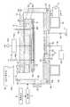
본 발명의 플라즈마 처리 장치의 일 실시형태에 대해, 도 1 내지 도 5를 참조해서 설명한다. 이 플라즈마 처리 장치는 처리 가스를 플라즈마화한 플라즈마에 의해, 기판인 반도체 웨이퍼(이하 「웨이퍼」라 함) W에 대해, 플라즈마 처리 예를 들면 에칭 처리를 실행하기 위한 장치이다. 이 웨이퍼(W)에 대해 간단하게 설명한다. 이 웨이퍼(W)는 예를 들면 소정의 패턴이 패터닝된 예를 들면 유기물로 이루어지는 포토 레지스트 마스크, 예를 들면 유기물로 이루어지는 반사 방지막, 아몰퍼스 카본막, 절연막(SiO2막이나 SiCOH막) 혹은 Poly-Si(다결정 실리콘)막, 및 예를 들면 무기막으로 이루어지는 에칭 정지막 등으로 이루어지는 적층막이 상측부터 이 순서로 실리콘막상에 적층되어 있다. 그리고, 이하에 설명하는 바와 같이, 이 플라즈마 처리 장치에 의해, 포토 레지스트 마스크에 형성된 패턴을 거쳐, 하층측의 적층막에 대해 에칭 처리에 의해 오목부가 형성되게 된다.EMBODIMENT OF THE INVENTION One Embodiment of the plasma processing apparatus of this invention is described with reference to FIGS. This plasma processing apparatus is an apparatus for performing a plasma process, for example, an etching process, on a semiconductor wafer (hereinafter referred to as "wafer") W serving as a substrate by a plasma obtained by converting a plasma into a processing gas. This wafer W will be described briefly. The wafer W is, for example, a photoresist mask made of an organic material, for example, a predetermined pattern is patterned, an antireflection film made of an organic material, an amorphous carbon film, an insulating film (SiO2 film or SiCOH film) or Poly- A lamination film made of an Si (polycrystalline silicon) film and an etching stop film made of, for example, an inorganic film is laminated on the silicon film in this order from above. As described below, the plasma processing apparatus allows the recessed portion to be formed by the etching process on the laminated film on the lower layer side through the pattern formed on the photoresist mask.
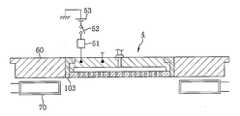
이 플라즈마 처리 장치는 진공 챔버로 이루어지는 처리 용기(21)와, 이 처리 용기(21)내의 저면 중앙에 배치된 탑재대(3)를 구비하고 있다. 처리 용기(21)는 전기적으로 접지되어 있다. 또한, 이 처리 용기(21)의 저면에 있어서의 탑재대(3)의 측방 위치에는 배기구(22)가 형성되어 있다. 이 배기구(22)에는 압력 조정 수단인 압력 조정 밸브(24a)를 구비한 배기관(24)을 거쳐서 진공 펌프 등을 포함하는 진공 배기 수단(23)이 접속되어 있다. 이들 압력 조정 밸브(24a) 및 진공 배기 수단(23)에 의해, 처리 용기(21)내를 진공 배기하기 위한 수단이 구성된다. 처리 용기(21)의 측벽에는 웨이퍼(W)의 반입 반출을 실행하기 위한 반송구(25)가 마련되어 있다. 이 반송구(25)는 게이트밸브(26)에 의해 개폐 가능하게 구성되어 있다.This plasma processing apparatus is provided with the
탑재대(3)는 하부전극(31)과, 이 하부전극(31)을 아래쪽측으로부터 지지하는 지지체(32)로 이루어지고, 처리 용기(21)의 저면에 절연 부재(33)를 거쳐서 배치되어 있다. 탑재대(3)의 상부에는 정전 척(34)이 마련되어 있고, 고압 직류 전원(35)으로부터 스위치(35a)에 의해 이 정전 척(34)에 전압이 인가되도록 되어 있다. 이것에 의해, 탑재대(3)상에 웨이퍼(W)가 정전 흡착된다.The mounting table 3 consists of a
탑재대(3)의 내부에는 온도 조절 매체가 통류하는 온도 조절 유로(37)가 형성되어 있고, 이 온도 조절 매체에 의해서 웨이퍼(W)의 온도를 조정하도록 구성되어 있다. 또한, 탑재대(3)의 내부에는 열전도성 가스를 백사이드 가스로서 웨이퍼(W)의 이면에 공급하기 위한 가스 유로(38)가 형성되어 있다. 이 가스 유로(38)는 탑재대(3)의 상면의 복수 개소에서 개구되어 있다. 기술한 정전 척(34)에는 이 가스 유로(38)에 연통하는 복수의 관통 구멍(34a)이 형성되어 있다. 상기의 백사이드 가스는 이 관통 구멍(34a)을 거쳐서 웨이퍼(W)의 이면측에 공급된다.The temperature
하부전극(31)에는 예를 들면 주파수가 13.56㎒, 전력이 0∼4000W의 바이어스용의 고주파전원(31a)이 정합기(31b)를 거쳐서 접속되어 있다. 이 고주파전원(31a)으로부터 공급되는 고주파 바이어스는 후술하는 바와 같이, 플라즈마 중의 이온을 웨이퍼(W)측에 끌어당기기 위한 것이다.For example, a high
또한, 이 하부전극(31)의 바깥둘레가장자리 위에는 정전 척(34)을 둘러싸도록, 포커스 링(39)이 배치되어 있다. 이 포커스 링(39)을 거쳐서, 플라즈마가 탑재대(3)상의 웨이퍼(W)에 집속하도록 구성되어 있다.The
또한, 이 탑재대(3)에 대향하도록, 처리 용기(21)의 천벽의 중앙부에, 내측 천판을 이루는 가스 샤워헤드(4)가 배치되어 있다. 이 가스 샤워헤드(4)는 하면측이 원형형상으로 움푹 패인 예를 들면 알루미늄 등의 도전성 부재로 이루어지는 전극부(42)와, 이 전극부(42)의 하면측을 덮도록 마련된 도전성 부재 예를 들면 다결정 실리콘으로 이루어지는 원판형상의 샤워 플레이트를 이루는 지지 부재(43)로 구성되어 있다. 도전성 부재는 이 예와 같이 반도체라도 좋지만, 도체 예를 들면 금속이라도 좋다. 이 전극부(42)와 지지 부재(43)에 의해 구획되는 공간이 처리 가스가 확산하는 가스 확산 공간(41)을 이룬다.Moreover, the
전극부(42)에는 스위치(52)를 거쳐서, 예를 들면 0∼-2000V의 부의 직류 전압을 인가하기 위한 직류 전원(53)이 부전압 공급 수단으로서 접속되어 있다. 이 직류 전원(53)은 플라즈마의 발생시에 가스 샤워헤드(4)의 아래쪽측의 영역에 인가 전압의 크기에 따른 두께의 시스를 형성하기 위한 것이다. 이 시스에 의해, 후술하는 유도 코일(70)에 의해 처리 영역의 둘레가장자리부에 형성(유도)되는 전계를, 해당 처리 영역의 중앙부측으로 끌어당길 수 있도록 되어 있다.A
전극부(42)의 중앙부에는 가스 확산 공간(41)과 연통하는 처리 가스 공급로(45)가 형성되어 있다. 이 처리 가스 공급로(45)의 상류측에는 가스 공급관(48)을 거쳐서 처리 가스 공급계(49)가 접속되어 있다. 이 처리 가스 공급계(49)는 웨이퍼(W)에 대해 처리 가스를 공급하기 위한 것이고, 이 예에서는 처리 가스로서 에칭 처리를 실행하기 위한 에칭 가스, 예를 들면 플로로카본 가스, 염소(Cl2) 가스, 일산화 탄소(CO) 가스, 취화 수소(HBr) 가스 혹은 O3(오존) 가스 등을, Ar (아르곤) 가스등의 희석 가스와 함께, 처리 용기(21)내에 공급할 수 있도록 구성되어 있다. 또한, 이 처리 가스 공급계(49)는 도시를 생략하고 있지만, 예를 들면 밸브나 유량 조정부가 개재된 복수의 분기로와, 이들 분기로의 각각에 접속되어 상기의 에칭 가스나 희석 가스가 저장된 가스원을 구비하고 있고, 에칭 처리를 실행하는 피에칭막의 종류에 따라, 소정의 에칭 가스나 Ar 가스를 원하는 유량비로 공급할 수 있도록 구성되어 있다.The process
지지 부재(43)는 예를 들면 상면의 둘레가장자리에 형성된 도시하지 않은 시일 부재 등을 거쳐서, 전극부(42)에 기밀하게 압착되어 있다. 또한, 지지 부재(43)에는 가스 확산 공간(41)으로부터 웨이퍼(W)에 대해 높은 면내 균일성을 갖고 가스를 공급할 수 있도록, 다수의 가스 토출 구멍(44)이 배열되어 있다. 이 예에서는 가스 샤워헤드(4)는 예를 들면 12인치의 웨이퍼(W)에 대해, 가장 바깥둘레의 가스 토출 구멍(44)이 처리 용기(21)의 중심에서 12.0㎝의 위치로 되도록 마련되어 있다. 무엇보다도, 가장 바깥둘레의 가스 토출 구멍(44)은 상기 중심에서 15㎝의 위치(웨이퍼(W)의 바깥가장자리)로 되도록 구성 내지 배치되어도 좋고, 반대로, 본 예보다도 중심 부근에 구성 내지 배치되어도 좋다. 가스 샤워헤드(4)의 사이즈를 어디까지 작게 할 수 있을지에 대해서는 웨이퍼(W)에 대한 가스 공급의 면내 균일성의 유효성이 얻어지는 범위내로 된다.The
처리 용기(21)의 천벽부에 있어서의 가스 샤워헤드(4)를 둘러싸는 링형상의 영역은 외측 천판(60)을 이루고, 유전체 예를 들면 석영 등에 의해 구성되어 있다. 이 외측 천판(60)과 가스 샤워헤드(4)는 예를 들면 해당 외측 천판(60)의 내주단에 링형상으로 형성된 도시하지 않은 시일 부재 등에 의해서 기밀하게 압착되어 있고, 또한 그들 하단면의 높이 위치가 동일한 높이로 되도록 고정되어 있다. 이 외측 천판(60)은 외주단에 있어서, 처리 용기(21)의 측벽에 의해 지지되어 있다. 여기서, 처리 용기(21)의 천벽(가스 샤워헤드(4) 및 외측 천판(60))이 해당 처리 용기(21)내에 들어가, 가스 샤워헤드(4)와 탑재대(3)가 근접하도록, 천벽의 외주단의 높이 위치가 그 내주측보다도 높게 되어 있다. 또한, 처리 용기(21)의 측벽의 상단부에는 둘레방향에 걸쳐 링형상의 홈(61)이 형성되어 있다. 이 홈(61)내에 예를 들면 O링 등의 시일 부재(62)가 수납되어 있다. 그리고, 예를 들면 처리 용기(21)내의 분위기가 기술한 진공 배기 수단(23)에 의해 진공화될 때, 외측 천판(60)이 처리 용기(21)측에 끌어당겨지고, 해당 시일 부재(62)에 의해서 처리 용기(21)의 기밀이 유지되게 된다.The ring-shaped region surrounding the
이 외측 천판(60)상에는 도 2에도 나타내는 바와 같이, 예를 들면 금속으로 이루어지는 도선이 각형으로 복수권 감긴 유도 도체인 유도 코일(70)이 둘레방향에 복수 개소 예를 들면 8개소에 등간격으로 마련되어 있다. 더욱 상세하게는 처리 용기(21)내의 수평면내에 있어서, 다각형(삼각형 이상), 이 예에서는 팔각형의 각 변에 상당하는 부위의 둘레에 도선이 감겨져, 각 유도 코일(70)이 구성되어 있다. 이 유도 코일(70)은 전자 유도에 의해, 외측 천판(60)을 거쳐서 처리 용기(21)내에 있어서의 해당 유도 코일(70)의 아래쪽측의 영역, 즉 가스 샤워헤드(4)의 아래쪽 공간을 둘러싸는 영역에 유도 결합형 플라즈마를 발생시키기 위한 것이고, 예를 들면 주파수가 13.56㎒, 전력이 500∼3000W의 고주파 전원(71)에 각각이 병렬로 접속되어 있다. 유도 코일(70)에 고주파 전류를 통전하는 것에 의해, 유도 코일(70)의 권선의 감기방향을 따른 전계 Er과 유도 코일(70)의 중심축에 직교하는 방향(연직방향)을 따른 전계 Ez가 발생한다. 여기서, 전계 Er이 처리 용기(21)의 둘레가장자리에서 중앙 및 중앙에서 둘레가장자리를 향하도록(처리 용기(21)의 직경방향에 생기도록), 유도 코일(70)이 배치되어 있다. 도 3에 있어서, 편의상 하나의 유도 코일(70)만을 확대해서 나타내고 있다. 또한, 도 2 및 도 3에서는 도시를 간략화하고 있지만, 이 유도 코일(70)은 다수 권취된 도선에 의해서 구성되어 있다. 기술한 도 1은 도 2에 있어서의 A-A선으로 처리 용기(21)를 절단했을 때의 종단면도에 상당하고 있다.On this outer
도 1에서는 기재를 생략하고 있지만, 가스 샤워헤드(4)는 냉각 수단을 구비하고 있다. 이 냉각 수단은 구체적으로는 예를 들면 도 4a 및 도 4b에 나타내는 바와 같이, 전극부(42)의 내부에 있어서 처리 가스 공급로(45)와 간섭하지 않도록 나선상으로 수평방향으로 둘러 형성된 온도 조절 유로(110)이다. 이 온도 조절 유로(110)내를 소정의 온도로 조절된 온도 조절 매체 예를 들면 물이 온도 조절 유체 통유로(111)를 거쳐서 통류하는 것에 의해, 해당 가스 샤워헤드(4)의 온도 조절이 가능하도록 구성되어 있다. 또한, 도 4a는 도 4b에 있어서의 A-A선으로 가스 샤워헤드(4)를 절단한 종단면도에 상당하고 있다.Although the base material is abbreviate | omitted in FIG. 1, the
또한, 도 5에도 나타내는 바와 같이, 해당 플라즈마 처리 장치에는 제어부(7)가 접속되어 있다. 이 제어부(7)는 CPU(11), 프로그램(을 기억한 프로그램 기억부)(12), 작업용의 워크 메모리(13), 및 데이터 기억부인 메모리(14)를 구비하고 있다. 메모리(14)에는 각 레시피마다 에칭 처리를 실행하는 막(피에칭막)의 종류, 에칭 가스의 종류, 가스 유량, 처리 압력, 유도 코일(70)에 공급하는 고주파 전력의 값, 직류 전원(53)에 인가하는 부의 직류 전압의 값 등의 처리 조건이 기입되는 영역이 마련되어 있다.5, the control unit 7 is connected to the plasma processing apparatus. This control unit 7 includes a
기술한 바와 같이, 웨이퍼(W)상에는 서로 종류가 다른 다층의 막이 적층되어 있다. 그 때문에, 이 다층막에 대해 에칭 처리를 실행하는 경우에는 각각의 막마다 에칭 가스의 종류가 다르고, 또한 각각의 막마다 에칭 가스의 유량이나 처리 압력 등도 다르다. 따라서, 웨이퍼(W)의 면내에 있어서 균일하게 에칭 처리를 실행하기 위해서는 각각의 막마다 면내에 있어서 에칭 가스를 균일하게 플라즈마화할 필요가 있다. 특히, 웨이퍼(W)의 직경방향에 있어서 균일한 플라즈마를 형성할 필요가 있다. 그래서, 본 실시형태에서는 가스 샤워헤드(4)에 인가하는 부의 직류 전압의 크기를 조정하는 것에 의해서, 유도 코일(70)에 의해 처리 영역의 둘레가장자리부에 형성되는 전계의 강도와, 해당 부의 직류 전압에 의해 처리 영역의 중앙부측에 인입하는 전계의 강도를 각각의 막마다 조정하여, 이 전계에 의해 형성되는 플라즈마의 양(농도)을 면내에 있어서 균일화하도록 하고 있다. 그 때문에, 예를 들면 실험이나 계산을 실행하여, 각각의 막(레시피)마다 가스 샤워헤드(4)에 인가해야 할 전압의 값을 미리 구해 두고, 이 값을 상기의 메모리(14)에 각각의 레시피마다 기억하도록 하고 있다. 또한, 이와 같이 레시피마다 미리 전압의 값을 구해 두지 않아도, 예를 들면 처리를 실행할 때마다 해당 값을 계산해서 구하도록 해도 좋다.As described above, multilayer films of different types are stacked on the wafer W. As shown in FIG. Therefore, when performing an etching process with respect to this multilayer film, the kind of etching gas differs for every film | membrane, and the flow volume of a etching gas, processing pressure, etc. differ for each film | membrane. Therefore, in order to perform the etching process uniformly in the surface of the wafer W, it is necessary to uniformly plasmamize the etching gas in the surface for each film. In particular, it is necessary to form a uniform plasma in the radial direction of the wafer (W). Therefore, in this embodiment, by adjusting the magnitude of the DC voltage of the part applied to the
상기의 프로그램(12)은 에칭 처리를 실행하는 막마다, CPU(11)를 거쳐서 메모리(14)로부터 기술한 레시피를 작업용의 워크 메모리(13)에 읽어내고, 이 레시피에 따라, 플라즈마 처리 장치의 각 부에 제어 신호를 보내고, 후술하는 각 스텝을 진행시킴으로써 에칭 처리를 실행한다는 명령이 내장되어 있다. 이 프로그램(처리 파라미터의 입력 조작이나 표시에 관한 프로그램도 포함)(12)은 예를 들면 하드 디스크, 컴팩트 디스크, 마그네트 옵티컬 디스크, 메모리카드 등의 기억 매체(8)에 저장되어, 해당 기억부(8)로부터 제어부(7)(의 프로그램 기억부(12))에 인스톨되는 것이 일반적이다.The program 12 reads the recipe described from the
다음에, 상기의 플라즈마 처리 장치의 작용에 대해, 도 6 내지 도 10을 참조해서 설명한다. 우선, 웨이퍼(W)의 표면에 형성된 피에칭막에 따른 레시피가 메모리(14)로부터 워크 메모리(13)에 읽어내어진다. 이 예에 있어서는 기술한 바와 같이, 표층의 피에칭이 예를 들면 반사 방지막이기 때문에, 이 막에 따른 레시피가 읽어내어진다. 그리고, 진공 분위기에 유지된 진공 반송실로부터 기판 반송 수단(모두 도시하지 않음)에 의해 처리 용기(21)내에 웨이퍼(W)가 반입되어, 탑재대(3)에 탑재된 후, 게이트밸브(26)가 닫힌다. 그리고, 진공 배기 수단(23)에 의해 처리 용기(21)내가 예를 들면 압력 조정 밸브(24a)가 완전 개방으로 된 상태로 되는 동시에, 온도 조절 유로(37) 및 가스 유로(38)로부터 소정의 온도로 조절된 온도 조절 매체 및 백사이드 가스가 공급되어, 웨이퍼(W)가 소정의 온도로 조정된다. 또한, 온도 조절 유체 통유로(111)로부터 소정의 온도로 조절된 온도 조절 매체를 온도 조절 유로(110)내에 통류시키는 것에 의해, 가스 샤워헤드(4)가 소정의 온도로 조절된다.Next, the operation of the plasma processing apparatus will be described with reference to FIGS. 6 to 10. First, a recipe corresponding to an etching target film formed on the surface of the wafer W is read from the
계속해서, 유도 코일(70)에 소정의 전력의 고주파 예를 들면 주파수가 13.56㎒, 전력이 2000W의 고주파를 공급해서 통전하는 동시에, 탑재대(3)에 고주파전원(31a)으로부터 바이어스용의 고주파를 공급한다. 유도 코일(70)에 고주파를 공급하는 것에 의해, 외측 천판(60)을 거쳐서 가스 샤워헤드(4)의 아래쪽 공간을 둘러싸는 영역에, 웨이퍼(W)의 직경방향으로 수평인 (처리 영역의 둘레가장자리부측에서 가스 샤워헤드(4)의 중심방향을 향하고, 및 중심방향에서 둘레가장자리부측을 향하는) 전계 Er과 연직방향의 전계 Ez로 이루어지는 TM 모드의 전계가 형성된다. 그리고, 가스 샤워헤드(4)에 소정 크기의 부의 예를 들면 -500V의 직류 전압이 인가된다. 이 부의 직류 전압에 의해, 해당 가스 샤워헤드(4)의 하면에 근접하는 위치에 부의 전계가 형성된다.Subsequently, a high frequency of predetermined power is supplied to the
다음에, 처리 가스 공급계(49)로부터 처리 용기(21)내에, 에칭 가스와 함께 예를 들면 Ar 가스가 공급되어, 처리 용기(21)내가 소정의 압력 예를 들면 2.67Pa(20mTorr)로 조정된다. Ar 가스는 저에너지로 활성화되기 때문에, 에칭 가스와 함께 처리 용기(21)내에 공급되는 것이 바람직하다. 이들 에칭 가스와 Ar 가스의 혼합 가스인 처리 가스는 처리 용기(21)내로 확산해 가고, 기술한 TM모드의 전계에 의해, 유도 코일(70)의 아래쪽 위치에 있어서 플라즈마화되어, Ar+이온이나 에칭 가스 재료의 이온 및 전자 등을 포함하는 유도 결합형 플라즈마가 생성된다. 그리고, 처리 영역의 둘레가장자리부측에 있어서 생성된 플라즈마는 처리 용기(21)내, 예를 들면 가스 샤워헤드(4)의 중앙부측으로 확산해 간다. 이 플라즈마에 의해, 해당 중앙부측의 가스도 플라즈마화된다. 이것에 의해, 처리 영역에서는 수평방향의 전체에 걸쳐 플라즈마(80)가 생성되게 된다. 여기서, 가스 샤워헤드(4)에 부의 직류 전압을 인가하지 않으면, 도 6에 나타내는 바와 같이 주로 유도 코일(70)의 아래쪽 위치에 있어서만 플라즈마가 생성되고, 중앙부측의 플라즈마 밀도가 둘레가장자리부측보다도 얇게 되어 버린다. 도 6에 있어서, 플라즈마 밀도가 높은 영역에 사선이 그어져 있다.Next, for example, Ar gas is supplied from the processing
그러나, 본 실시형태에서는 기술한 바와 같이, 가스 샤워헤드(4)에 부의 직류 전압이 인가되므로, 가스 샤워헤드(4)의 하면에 근접하는 영역에 부의 전계가 형성된다. 따라서, 이 바로 아래에 두꺼운 DC 시스(75)가 형성된다. 이 DC 시스(75)는 부의 직류 전압의 크기에 따른 두께로 된다. 그리고, 전계 Er이 가스 샤워헤드(4)의 중앙부측을 향해, DC 시스(75)내를 침투하고, 이것에 의거하여, 웨이퍼(W)의 면내에 걸쳐서 균일성이 높은 플라즈마가 생성된다. 그 이유에 대해서는 다음과 같이 추측할 수 있다. 도 7에 나타내는 바와 같이, 유도 코일(70)의 아래쪽측의 플라즈마가 이 전계 Er에 수반하여 해당 DC 시스(75)내에 들어가므로, 또한, 중앙부측에 침투한 전계 Er에 의해 해당 중앙부측에서도 처리 가스가 플라즈마화되어 가므로, DC 시스(75)와 그 아래쪽의 플라즈마 영역의 경계부분, 혹은 이것에 가까운 부분에 있어서 플라즈마의 밀도가 짙게 되어 간다. 그 때문에, 도 8에 나타내는 바와 같이, DC 시스(75)의 아래쪽측에 있어서도, 유도 코일(70)의 아래쪽측과 마찬가지로 밀도가 짙은 플라즈마가 형성된다.However, in the present embodiment, as described above, since a negative direct current voltage is applied to the
그리고, 플라즈마(80)중의 전자가 에칭 가스나 Ar 가스와 충돌하면, 이들 가스가 플라즈마화되고, 또한, 이 플라즈마화에 의해 생성된 전자가 순차 에칭 가스나 Ar 가스에 충돌해 가는 것에 의해서, 순차 플라즈마화가 진행하여, 플라즈마(80)가 고밀도화되어 간다. 이와 같이 해서, 유도 코일(70)에 의해 생성된 고밀도의 유도 결합형 플라즈마가 소위 DC 시스(75)를 거쳐서 가스 샤워헤드(4)의 아래쪽측으로 확대되어 가는 동시에, 아래쪽측을 향하는 배기류를 타고 웨이퍼(W)상으로 하강해서, 웨이퍼(W)의 면내에 걸쳐 균일성이 높은 플라즈마(80)가 형성되게 된다.When the electrons in the
또한, 도 9에 나타내는 바와 같이, 플라즈마중의 플러스의 이온, 예를 들면 상기의 Ar+이온이 DC 시스(75)의 부의 전계에 강하게 끌어당겨져 샤워헤드(4)에 충돌하고, 이 충돌에 의해, 가스 샤워헤드(4)로부터 2차 전자가 발생하여, DC 시스(75)내에 있어서 이 2차 전자가 가속되어 아래쪽측으로 돌출되고, 이 2차 전자에 의해 처리 가스가 플라즈마화된다고 하는 효과도 있다. 이 때문에, 웨이퍼(W)의 위쪽의 플라즈마(80)는 밀도가 더욱 높아지고, 또한 면내에 있어서 더욱 균일화되어 가게 된다.In addition, as shown in FIG. 9, positive ions in the plasma, for example, Ar+ ions, are strongly attracted to the negative electric field of the
그리고, 도 10에 나타내는 바와 같이, 플라즈마중의 이온이 고주파전원(31a)에 의한 고주파 바이어스에 의해서 웨이퍼(W)측에 끌어당겨짐으로써, 수직성이 높은 에칭 처리가 진행해 가게 된다. 이와 같이 해서, 반사 방지막의 하층의 아몰퍼스 카본막이 노출될 때까지, 해당 반사 방지막의 에칭 처리가 실행된다.And as shown in FIG. 10, the ion processing in a plasma is attracted to the wafer W side by the high frequency bias by the high
그 후, 에칭 가스 및 Ar 가스의 공급이 정지되는 동시에, 유도 코일(70)에의 고주파의 공급과 가스 샤워헤드(4)에의 부의 직류 전압의 인가가 정지된다. 그리고, 처리 용기(21)내가 진공 배기되어, 계속해서 에칭 처리를 실행하는 막인 아몰퍼스 카본막에 따른 레시피가 메모리(14)로부터 읽어내어지고, 이 아몰퍼스 카본막의 에칭 처리가 시작된다. 그 후, 아몰퍼스 카본막의 하층측의 막에 대해, 마찬가지로 순차 레시피가 읽어내어져, 에칭 처리가 실행되어 간다.Thereafter, the supply of the etching gas and the Ar gas is stopped, and the supply of the high frequency to the
상술한 실시형태에 의하면, 처리 용기(21)의 천벽의 중앙부에 도전성 부재로 이루어지는 가스 샤워헤드(4)가 마련되어, 웨이퍼(W)에 대해 면내 균일성이 높다고 하는 형태로 가스의 공급이 실행되는 한편, 가스 샤워헤드(4)의 아래쪽 공간을 둘러싸는 영역에 유도 코일(70)에 의해서 유도 결합형 플라즈마가 발생되고, 또한, 가스 샤워헤드(4)에 부의 직류 전압을 인가함으로써 그 아래쪽에 DC 시스(75)가 형성되고, 해당 DC 시스(75)를 거쳐서 상기 플라즈마가 중앙부측으로 확대되도록 되어 있다. 따라서, 유도 결합형 플라즈마를 이용하는 형태이면서, 가스 샤워헤드(4)를 이용하여 균일성이 높은 가스의 공급을 실행할 수 있고, 더구나 가스 샤워헤드(4)의 아래쪽측 공간도 포함시켜 웨이퍼(W)의 면을 따라 균일성이 높은 플라즈마(80)를 발생시킬 수 있다. 이 때문에, 웨이퍼(W)에 대해 면내 균일성이 높은 플라즈마 처리, 이 예에서는 에칭 처리를 실현할 수 있다.According to the above-mentioned embodiment, the
그리고, 가스 샤워헤드(4)에 인가하는 부의 직류 전압에 의해서, DC 시스(75)의 두께를 조정하는 것에 의해서, 처리 레시피에 따른 면내 균일성이 높은 적절한 플라즈마(80)를 용이하게 얻을 수 있다. 유도 결합형 플라즈마(80)는 이 플라즈마 처리 장치와 같이, 처리 용기(21)의 천판(외측 천판(60))의 위에 유도 코일(70)을 마련하는 것만으로 발생시킬 수 있으므로, 장치 구성이 간이하고 비용적으로 유리하다. 한편, 종래의 유도 결합형 플라즈마 방식은 면적이 큰 기판에 대해, 가스의 공급 등의 점에서 불리하다고 되어 있었지만, 본 실시형태의 플라즈마 처리 장치에서는 그와 같은 불리가 없다.And by adjusting the thickness of the
또한, 상술한 장치는 Ar+이온의 충격에 의해서, 소위 스퍼터와 같이 가스 샤워헤드(4)가 물리적으로 깎여 버리는 것도 고려되지만, 가스 샤워헤드(4)의 하면이 실리콘으로 구성되어 있으므로, 오염의 우려가 없다. 또한, 가스 샤워헤드(4)로부터 균일하게 에칭 가스가 공급되므로, 해당 가스 샤워헤드(4)와 탑재대(3)를 근접시킬 수 있고, 처리 용기(21)의 높이를 억제할 수 있다. 또한, 지지 부재(43)에 온도 조절 유로(110)를 둘러 형성하는 것에 의해, 레시피에 따라 가스 샤워헤드(4)의 온도를 조정할 수 있다.In addition, although the above-mentioned apparatus considers that the
상기의 예에 있어서는 가스 샤워헤드(4)에 인가하는 부의 직류 전압의 값을 조정하여, 면내에 있어서의 플라즈마 밀도를 균일화하도록 했지만, 이 부의 직류 전압의 값과 함께 유도 코일(70)에 공급하는 고주파의 전력을 조정하여, 플라즈마 밀도를 균일화하도록 해도 좋고, 혹은 부의 직류 전압을 소정의 값으로 고정시켜 유도 코일(70)에 공급하는 고주파 전력의 크기를 조정하여, 플라즈마 밀도를 균일화하도록 해도 좋다.In the above example, the value of the negative DC voltage applied to the
상술한 실시형태에서는 유도 코일(70)을 각형으로 감고 있기 때문에, 처리 용기(21)의 둘레가장자리에서 중앙 및 중앙에서 둘레가장자리를 향하는 큰 전계 Er이 얻어지는 점에서 유리하다. 무엇보다도, 유도 코일(70)로서는 예를 들면 그 장축이 처리 용기(21)의 둘레가장자리에서 중앙을 향해 신장하는 방향인 것과 같은 타원형상으로 감은 것이어도 좋고, 혹은 진원형상으로 감은 것이어도 좋다. 또한, 처리 용기(21)내에 전계를 발생시키기 위해서는 유도 코일(70)을 이용하는 대신, 예를 들면 다수의 봉형상의 안테나를 처리 용기(21)의 중심부에서 둘레가장자리부를 향해 방사상으로 배치해도 좋다.In the above-described embodiment, since the
또한, 상술한 실시형태에서는 유도 코일(70)을 따라 형성되는 전계 Er 중 처리 용기(21)내에 발생하는 전계 Er이 처리 용기(21)의 중앙을 향하도록, 평면에서 보아 처리 용기(21)의 중심부를 중심으로 하는 팔각형의 각 변의 둘레에 각 유도 코일(70)을 구성하고 있지만, 도 11에 나타내는 바와 같이, 수평면내에서 상기 각 변에 대해 비스듬히 향한 축의 둘레에 각 유도 코일(70)을 감아 구성해도 좋다. 이 경우에도, 상기 전계 Er에 대해 처리 용기(21)의 둘레가장자리에서 중앙을 향하는 성분이 존재하고, 해당 전계성분이 DC 시스(75)의 내에 들어가게 된다. 그리고 또한, 각 유도 코일(70)마다 임피던스 조정을 실행하는 조정부를 마련하여, 독립적으로 고주파 전류의 크기를 조정하도록 해도 좋다. 또한, 각 유도 코일(70)은 병렬로 접속하는 대신, 직렬로 접속해도 좋다. 또는 각 유도 코일(70)마다 고주파전원을 준비하여, 각 유도 코일(70)마다 공급하는 고주파 전류의 크기를 조정하도록 해도 좋다.In addition, in the above-described embodiment, the planar bore of the
상기의 예에 있어서는 유도 코일(70)을 외측 천판(60)의 위쪽에 설치하도록 했지만, 도 12에 나타내는 바와 같이, 외측 천판(60)을 상측부분(100)과 하측부분(101)으로 이루어지는 분할 구조체로서 구성하는 동시에, 이 하측부분(101)에 예를 들면 둘레방향으로 복수의 오목부(102)를 등간격으로 형성하여, 이 오목부(102)내에 유도 코일(70)을 수납해도 좋다. 이 경우에 있어서도, 상기의 예와 마찬가지의 작용이 얻어지고, 즉, 에칭 가스가 균일하게 플라즈마화되어 면내에 있어서 균일하게 에칭 처리가 실행되게 된다. 또한, 이와 같이 외측 천판(60)의 내부에 유도 코일(70)을 수납하는 것 이외에도, 예를 들면 외측 천판(60)의 아래쪽위치에 있어서의 처리 용기(21)내에 유도 코일(70)을 설치하도록 해도 좋다. 이 경우에는 도 13에 나타내는 바와 같이, 외측 천판(60)을 예를 들면 도전성 부재에 의해 구성하여, 외측 천판(60)과 가스 샤워헤드(4) 사이에 절연 부재(103)를 개재시키는 것이 바람직하다.In the above example, the
또한, 상기의 예에서는 유도 코일(70)을 둘레방향으로 복수 개소에 설치하도록 했지만, 도 14에 나타내는 바와 같이, 유도 코일(70)을 둘레방향에 걸쳐 1개로 연결하여 배치하도록 해도 좋다. 이 경우에도, 처리 용기(21)내에 있어서 둘레가장자리측에서 중앙부측을 향하는 전계 Er이 발생하므로, 가스 샤워헤드(4)의 아래쪽측의 DC 시스(75)내에 전계 Er이 침투하고, 기술한 실시형태와 마찬가지의 효과가 얻어진다.In addition, in the above example, the induction coils 70 are provided at plural places in the circumferential direction, but as shown in FIG. 14, the induction coils 70 may be connected and arranged in one in the circumferential direction. Also in this case, since the electric field Er is generated from the peripheral edge side toward the center portion side in the
또한, 처리 용기(21)내에 전계를 형성하기 위해서는 단상 코일에 한정되지 않고, 예를 들면 스타 결선 혹은 △결선된 삼상 코일을 처리 용기(21)의 둘레방향에 배치하도록 해도 좋다. 또한, 가스 샤워헤드(4)에 있어서, 처리 영역측의 샤워 플레이트만을 도전성 부재에 의해 구성하고, 이 샤워 플레이트와 직류 전원(53)을 도전로로 접속해서 샤워 플레이트에 부의 전압을 인가하는 경우에도, 본 발명의 기술범위에 포함된다.In addition, in order to form an electric field in the
상기의 각 예에 있어서는 플라즈마 처리로서 에칭 처리를 예로 들어 설명했지만, 본 발명의 플라즈마 처리 장치를, 예를 들면 플라즈마를 이용한 CVD(Chemical Vapor Deposition)법을 이용한 성막처리 장치에 적용해도 좋고, 애싱 장치에 적용해도 좋다. 예를 들면 성막 장치에 있어서는 성막 가스의 종류나 유량, 압력 등의 처리 조건에 따라, 가스 샤워헤드(4)에 인가되는 부의 직류 전압의 크기가 조정되어, 면내에 있어서 균일한 성막속도로 성막처리가 실행되게 된다.In each of the above examples, the etching treatment is described as an example of plasma processing. However, the plasma processing apparatus of the present invention may be applied to a film forming apparatus using, for example, a CVD (Chemical Vapor Deposition) method using plasma. You may apply to. For example, in the film forming apparatus, the magnitude of the negative DC voltage applied to the
(실험)(Experiment)
다음에, 기술한 바와 같이, 부의 직류 전원(53)으로부터 가스 샤워헤드(4)에 부의 직류 전압을 인가하는 것에 의해, 전자 밀도가 어떻게 변화하는지 확인하기 위해 CCP 장치를 이용하여 실행한 실험에 대해 설명한다.Next, as described above, about an experiment performed using a CCP apparatus to confirm how the electron density changes by applying a negative DC voltage from the negative
전자 밀도 측정 프로브를 이용하여, 가스 샤워헤드(4)에 부의 직류 전압(900V)을 인가했을 때와, 부의 직류 전압을 인가하지 않았을 때의 해당 가스 샤워헤드(4)의 아래쪽에 있어서의 전자 밀도의 차가 비교되었다.The electron density in the lower part of the said
(결과)(result)
도 15에 나타내는 바와 같이, 가스 샤워헤드(4)에 부의 직류 전압을 인가하는 것에 의해, 가스 샤워헤드(4)의 아래쪽측에 있어서의 전자 밀도가 증가하는 것을 알 수 있었다. 즉, 가스 샤워헤드(4)와 탑재대(3) 사이의 플러스 이온이 DC 시스에 의해 가스 샤워헤드(4)측으로 끌어당겨지고, 또한, 플라즈마중의 플러스 이온(Ar+)이 가스 샤워헤드(4)에 충돌하여, 전자가 생성한다고 하는 것을 알 수 있다.As shown in FIG. 15, it turned out that the electron density in the lower side of the
또한, 도시는 생략하겠지만, 별도로 실행한 계산이나 실험에 의해, 가스 샤워헤드(4)에 200V 이상의 부의 직류 전압을 인가함으로써, 전자 밀도가 증가하는 것을 알 수 있었다.In addition, although illustration is abbreviate | omitted, it turned out that the electron density increases by applying the negative DC voltage of 200 V or more to the
(시뮬레이션)(simulation)
다음에, 기술한 도 3에 나타내는 바와 같이 유도 코일(70)을 감는 동시에, 가스 샤워헤드(4)에 부의 직류 전압을 인가했을 때에, 처리 용기(21)내에 형성되는 TM모드의 전계의 밀도분포가 어떻게 변화하는지 확인하기 위해, 전자계 계산 소프트인 COMSOL을 이용하여 시뮬레이션(계산)을 실행하였다.Next, as shown in FIG. 3 described above, when the
유도 코일(70)에 13.56㎒, 1500W의 고주파를 공급한 경우에 대해 계산을 실행하였다. 또한, 가스 샤워헤드(4)에 부의 직류 전압을 인가하는 것에 의해, 가스 샤워헤드(4)의 아래쪽측에 형성되는 DC 시스(75)의 두께가 1㎜, 5㎜, 10㎜로 되는 경우에 대해 각각 계산을 실행하였다. 그리고, 처리 용기(21)의 중앙으로부터 우측 절반에 대해, 처리 가스에 흡수되는 전계강도를 조사하였다. 이 흡수 전계강도(처리 가스에 흡수되는 전계의 강도)에 의해서, DC 시스(75)의 아래쪽측의 플라즈마의 전자 밀도를 평가할 수 있다.The calculation was performed for the case where a high frequency of 13.56 MHz and 1500 W was supplied to the
(결과)(result)
도 16(a)에 나타내는 바와 같이, DC 시스 두께가 1㎜인 경우에도, DC 시스(75)의 아래쪽측에 있어서의 흡수 전계강도가 처리 용기(21)의 중앙부에 근접하는 영역까지 크게 되어 있다. 이것으로부터, TM모드의 전계가 웨이퍼(W)의 중앙부측을 향해 길게 신장되어 있는 것을 알 수 있었다. 또한, 도 16(b) 및 도 16(c)에 나타내는 바와 같이, DC 시스의 두께를 늘려가는 것에 의해, 즉 가스 샤워헤드(4)에 인가하는 부의 직류 전압을 크게 해 가는 것에 의해, 유도 코일(70)의 아래쪽측에 형성되는 TM모드의 전계가 웨이퍼(W)의 중앙부측을 향해 더욱 끌어당겨져 신장해 가는 것을 알 수 있었다.As shown in Fig. 16 (a), even when the thickness of the DC sheath is 1 mm, the absorbed electric field strength at the lower side of the
(비교 시뮬레이션)(Comparison Simulation)
다음에, 일본 특허 공개 공보 제2008-109155호의 장치와 마찬가지로, 웨이퍼(W)의 둘레가장자리부와 동심원형상의 전계(θ방향의 전계: TE모드)가 형성되도록, 코일을 웨이퍼(W)와 동심원형상으로 감은 경우에 대해, 상기와 마찬가지의 시뮬레이션 계산을 실행하였다.Next, similarly to the apparatus of Japanese Patent Laid-Open Publication No. 2008-109155, the coil is concentric with the wafer W so that a circumferential edge of the wafer W and an electric field of concentric circles (electric field in the θ direction: TE mode) are formed. About the case where it wound to the shape, simulation calculation similar to the above was performed.
(결과)(result)
그 결과, 도 17에 나타내는 바와 같이, 흡수 전계강도가 큰 영역은 코일의 아래쪽 위치에서만, 웨이퍼(W)의 중앙부측에는 전계가 신장하지 않고 있는 것을 알 수 있었다. 또, DC 시스의 두께가 증가한 경우에도, 이 경향에서는 큰 변화가 고려되지 않았다. 이것으로부터, 코일에 의해 형성되는 전계를 웨이퍼(W)의 중앙부측으로 연신시키기 위해서는 TM모드의 전계를 형성할 필요가 있는 것을 알 수 있다.As a result, as shown in FIG. 17, it turned out that the electric field does not extend to the center part side of the wafer W only in the position where the absorption electric field intensity is large, only below the coil. Moreover, even when the thickness of the DC sheath increased, a large change was not considered in this tendency. This shows that it is necessary to form the electric field of TM mode in order to extend the electric field formed by the coil to the center part side of the wafer W. As shown in FIG.
따라서, 기술한 바와 같이, 본 발명에 있어서의 유도 코일(70)은 전계 Er과 전계 Ez가 형성되도록, 웨이퍼(W)의 직경방향으로 대략 평행한 부분과, 연직방향으로 대략 평행한 부분이 형성되는 바와 같은 형태로 감길 필요가 있다.Therefore, as described above, in the
다음에, 본 발명의 플라즈마 처리 장치를 플라즈마 에칭 처리 장치에 적용한 일 실시형태에 대해, 도 18 내지 도 26을 참조해서 설명한다.Next, an embodiment in which the plasma processing apparatus of the present invention is applied to a plasma etching processing apparatus will be described with reference to FIGS. 18 to 26.
이 플라즈마 처리 장치는 진공 챔버로 이루어지는 처리 용기(1021)와, 이 처리 용기(1021)내의 저면 중앙에 배치된 탑재대(1003)를 구비하고 있다. 처리 용기(1021)는 전기적으로 접지되어 있다. 또한, 이 처리 용기(1021)의 저면에 있어서의 탑재대(1003)의 측방 위치에는 배기구(1022)가 형성되어 있다. 이 배기구(1022)에는 압력 조정 수단인 압력조정 밸브(1024a)를 구비한 배기관(1024)을 거쳐서 진공펌프 등을 포함하는 진공 배기 수단(1023)이 접속되어 있다. 이들 압력조정 밸브(1024a) 및 진공 배기 수단(1023)에 의해, 처리 용기(1021)내를 진공 배기하기 위한 수단이 구성된다. 처리 용기(1021)의 측벽에는 웨이퍼(W)의 반입 반출을 실행하기 위한 반송구(1025)가 마련되어 있다. 이 반송구(1025)는 게이트밸브(1026)에 의해 개폐 가능하게 구성되어 있다.This plasma processing apparatus is provided with the
탑재대(1003)는 하부전극(1031)과, 이 하부전극(1031)을 아래쪽측으로부터 지지하는 지지체(1032)로 이루어지고, 처리 용기(1021)의 저면에 절연 부재(1033)를 거쳐서 배치되어 있다. 탑재대(1003)의 상부에는 정전 척(1034)이 마련되어 있고, 고압 직류 전원(1035)으로부터 스위치(1035a)에 의해 이 정전 척(1034)에 전압이 인가되도록 되어 있다. 이것에 의해, 탑재대(1003)상에 웨이퍼(W)가 정전 흡착된다.The mounting table 1003 includes a
탑재대(1003)의 내부에는 온도 조절 매체가 통류하는 온도 조절 유로(1037)가 형성되어 있고, 이 온도 조절 매체에 의해서 웨이퍼(W)의 온도를 조정하도록 구성되어 있다. 또한, 탑재대(1003)의 내부에는 열전도성 가스를 백사이드 가스로서 웨이퍼(W)의 이면에 공급하기 위한 가스 유로(1038)가 형성되어 있다. 이 가스 유로(1038)는 탑재대(1003)의 상면의 복수 개소에서 개구되어 있다. 기술한 정전 척(1034)에는 이 가스 유로(1038)에 연통하는 복수의 관통 구멍(1034a)이 형성되어 있다. 상기의 백사이드 가스는 이 관통 구멍(1034a)을 거쳐서 웨이퍼(W)의 이면측에 공급된다.The temperature
하부전극(1031)에는 예를 들면 주파수가 20㎒, 전력이 0∼4000W의 바이어스용의 고주파전원(1031a)이 정합기(1031b)를 거쳐서 접속되어 있다. 이 고주파 전원(1031a)으로부터 공급되는 고주파 바이어스는 후술하는 바와 같이, 플라즈마중의 이온을 웨이퍼(W)측에 끌어당기기 위한 것이다.For example, a high
또한, 이 하부전극(1031)의 바깥둘레가장자리 위에는 정전 척(1034)을 둘러싸도록, 포커스 링(1039)이 배치되어 있다. 이 포커스링(1039)을 거쳐서, 플라즈마가 탑재대(1003)상의 웨이퍼(W)에 집속하도록 구성되어 있다.The
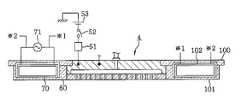
또한, 이 탑재대(1003)에 대향하도록, 처리 용기(1021)의 천벽의 중앙부에 내측 천판을 이루는 가스 샤워헤드(1004)가 배치되어 있다. 이 가스 샤워헤드(1004)는 하면측이 원형형상으로 움푹 패인 예를 들면 알루미늄 등의 도전성 부재로 이루어지는 전극부(1042)와, 이 전극부(1042)의 하면측을 덮도록 마련된 도전성 부재 예를 들면 다결정 실리콘으로 이루어지는 원판형상의 샤워 플레이트를 이루는 지지 부재(1043)로 구성되어 있다. 도전성 부재는 이 예와 같이 반도체라도 좋지만, 도체 예를 들면 금속이라도 좋다. 이 전극부(1042)와 지지 부재(1043)에 의해 구획되는 공간이 처리 가스가 확산하는 가스 확산 공간(1041)을 이룬다.Moreover, the
전극부(1042)에는 스위치(1052)를 거쳐서, 예를 들면 0∼-2000V의 부의 직류 전압을 인가하기 위한 직류 전원(1053)이 부전압 공급 수단으로서 접속되어 있다. 이 직류 전원(1053)은 플라즈마의 발생시에 가스 샤워헤드(1004)의 아래쪽측의 영역에 인가 전압의 크기에 따른 두께의 시스를 형성하기 위한 것이다. 이 시스에 의해서, 후술하는 안테나 유닛(1070)에 의해 처리 영역의 둘레가장자리부에 형성(유도)되는 전계를 해당 처리 영역의 중앙부측으로 끌어당길 수 있도록 되어 있다.A
전극부(1042)의 중앙부에는 가스 확산 공간(1041)과 연통하는 처리 가스 공급로(1045)가 형성되어 있다. 이 처리 가스 공급로(1045)의 상류측에는 가스 공급관(1048)을 거쳐서, 처리 가스 공급계(1049)가 접속되어 있다. 이 처리 가스 공급계(1049)는 웨이퍼(W)에 대해 처리 가스를 공급하기 위한 것이고, 이 예에서는 처리 가스로서 에칭 처리를 실행하기 위한 에칭 가스, 예를 들면 플로로카본가스, 염소(Cl2)가스, 일산화 탄소(CO) 가스, 취화 수소(HBr) 가스 혹은 O3(오존) 가스 등을, Ar (아르곤) 가스 등의 희석 가스와 함께, 처리 용기(1021)내에 공급할 수 있도록 구성되어 있다. 또한, 이 처리 가스 공급계(1049)는 도시를 생략하고 있지만, 예를 들면 밸브나 유량 조정부가 개재된 복수의 분기로와, 이들 분기로의 각각에 접속되어 상기의 에칭 가스나 희석 가스가 저장된 가스원을 구비하고 있고, 에칭 처리를 실행하는 피에칭막의 종류에 따라, 소정의 에칭 가스나 Ar 가스를 원하는 유량비로 공급할 수 있도록 구성되어 있다.The process
지지 부재(1043)는 예를 들면 상면의 둘레가장자리에 형성된 도시하지 않은 시일 부재 등을 거쳐서, 전극부(1042)에 기밀하게 압착되어 있다. 또한, 지지 부재(1043)에는 가스 확산 공간(1041)으로부터 웨이퍼(W)에 대해 높은 면내 균일성을 갖고 가스를 공급할 수 있도록, 다수의 가스 토출 구멍(1044)이 배열되어 있다. 이 예에서는 가스 샤워헤드(1004)는 예를 들면 12인치의 웨이퍼(W)에 대해, 가장 바깥둘레의 가스 토출 구멍(1044)이 처리 용기(1021)의 중심에서 12.0㎝의 위치로 되도록 마련되어 있다. 무엇보다도, 가장 바깥둘레의 가스 토출 구멍(1044)은 상기 중심에서 15㎝의 위치(웨이퍼(W)의 바깥둘레)로 되도록 구성 내지 배치되어도 좋고, 반대로, 본 예보다도 중심 부근에 구성 내지 배치되어도 좋다. 가스 샤워헤드(4)의 사이즈를 어디까지 작게 할 수 있을지에 대해서는 웨이퍼(W)에 대한 가스 공급의 면내 균일성의 유효성이 얻어지는 범위내로 하게 된다.The supporting
처리 용기(1021)의 천벽부에 있어서의 가스 샤워헤드(4)를 둘러싸는 링형상의 영역은 외측 천판(1060)을 이루고, 유전체 예를 들면 석영 등에 의해 구성되어 있다. 이 외측 천판(1060)과 가스 샤워헤드(1004)는 예를 들면 해당 외측 천판(1060)의 내주단에 링형상으로 형성된 도시하지 않은 시일 부재 등에 의해서 기밀하게 압착되어 있고, 또한, 그들 하단면의 높이 위치가 동일한 높이로 되도록 고정되어 있다. 이 외측 천판(1060)은 외주단에 있어서 처리 용기(1021)의 측벽에 의해 지지되어 있다. 여기서, 처리 용기(1021)의 천벽(가스 샤워헤드(1004) 및 외측 천판(1060))이 해당 처리 용기(1021)내에 들어가, 가스 샤워헤드(1004)와 탑재대(1003)가 근접하도록, 천벽의 외주단의 높이 위치가 그 내주측보다도 높게 되어 있다. 또한, 처리 용기(1021)의 측벽의 상단부에는 둘레방향에 걸쳐 링형상의 홈(1061)이 형성되어 있다. 이 홈(1061)내에, 예를 들면 O링 등의 시일 부재(1062)이 수납되어 있다. 그리고, 예를 들면 처리 용기(1021)내의 분위기가 기술한 진공 배기 수단(1023)에 의해 진공화될 때, 외측 천판(1060)이 처리 용기(1021)측으로 끌어당겨지고, 해당 시일 부재(1062)에 의해서 처리 용기(1021)의 기밀이 유지되게 된다.The ring-shaped region surrounding the
이 외측 천판(1060)상에는 도 19에도 나타내는 바와 같이, 둘레방향에 걸쳐 복수 개소 예를 들면 8개소에 등간격으로 되도록, 마이크로파 공급부를 이루는 안테나 모듈(1071)이 마련되어 있다. 이 안테나 모듈(1071)은 해당 안테나 모듈(1071)의 아래쪽측의 영역, 즉 가스 샤워헤드(1004)의 아래쪽공간을 둘러싸는 영역에, 마이크로파의 전계에 의해서 플라즈마를 발생시키기 위한 것이고, 마이크로파 출력부(1080)에 각각이 병렬로 접속되어 있다. 그리고, 안테나 모듈(1071)에 마이크로파를 공급하고, 후술하는 바와 같이 도 23에 나타내는 바와 같은 슬롯 배치를 채용하는 것에 의해, 둘레방향에 걸쳐 처리 용기(1021)의 둘레가장자리에서 중앙 및 중앙에서 둘레가장자리를 향하는 전계 Er이 형성되게 된다. 이들 복수의 안테나 모듈(1071)에 의해, 안테나 유닛(1070)이 구성된다.On this outer
마이크로파 출력부(1080)는 도 20에도 나타내는 바와 같이, 예를 들면 500∼3000W의 전력을 공급하기 위한 전원부(1081)와, 예를 들면 2.45㎓의 주파수의 마이크로파를 발진시키기 위한 마이크로파 발진기(1082)와, 발진된 마이크로파를 증폭하는 앰프(1083)와, 마이크로파를 각 안테나 모듈(1071)에 분배하기 위한 분배기(1084)를 구비하고 있다. 각각의 안테나 모듈(1071)은 분배기(1084)에서 분배된 마이크로파를 증폭하는 앰프부(1072)와, 임피던스를 정합시키기 위한 튜너(1073)와, 증폭된 마이크로파를 처리 용기(1021)내에 방사하는 안테나부(1074)를 구비하고 있다. 앰프부(1072)는 위상기(1075)와, 안테나 모듈(1071)에 공급되는 마이크로파의 전력 레벨을 각각의 안테나 모듈(1071)마다 조정하기 위한 가변 이득 앰프(1076)와, 솔리드 스테이트 앰프를 구성하는 메인 앰프(1077)와, 안테나부(1074)에서 반사되어 메인 앰프(1077)로 되돌리는 반사 마이크로파를 분리하기 위한 아이솔레이터(1078)를 구비하고 있다.As shown in Fig. 20, the
위상기(1075)는 슬래그 튜너에 의해 마이크로파의 위상을 변화시킬 수 있도록 구성되어 있고, 이 슬래그 튜너를 조정하는 것에 의해 마이크로파의 방사 특성을 변조시킬 수 있다. 이 슬래그 튜너에 의해, 위상기(1075)는 예를 들면 각 안테나 모듈(1071)마다 마이크로파의 위상을 조정함으로써 지향성을 제어하여 플라즈마 분포를 변화시킬 수 있다. 혹은 예를 들면 인접하는 안테나 모듈(1071, 1071)에 있어서 후술하는 슬롯(1101a)의 방향을 90° 씩 변경하는 것에 의해, 인접하는 안테나 모듈(1071)에 있어서 90° 씩 마이크로파의 위상을 어긋나게 하여, 원(圓) 편파를 얻을 수도 있다. 또한, 이러한 방사 특성의 변조가 불필요한 경우에는 위상기(1075)를 마련하지 않아도 좋다.The
계속해서, 기술한 안테나 모듈(1071)의 구체적인 구성에 대해 설명한다. 튜너(1073)와 안테나부(1074)는 도 21에 나타내는 바와 같이, 하측이 외측으로 부풀어오른 대략 원통형상이고 동축관의 외측 도체를 이루는 예를 들면 금속제의 하우징(1100)내에, 상측부터 이 순서로 수납되어 있다. 하측의 안테나부(1074)는 도 22에 나타내는 바와 같이, 원호형상의 2개의 슬롯(1101a)이 서로 대향하도록 형성된 대략 원판형상의 평면 슬롯 안테나(1101)와, 이 평면 슬롯 안테나(1101)의 상측에 마련되고 진공 분위기 중에서의 마이크로파의 파장을 짧게 하여 플라즈마의 밀도를 조정하기 위한 링형상의 지파재(1105)와, 평면 슬롯 안테나(1101)의 하측에 마련되고 유전체 부재 예를 들면 석영이나 세라믹스 등으로 이루어지는 천판(1106)을 구비하고 있다. 평면 슬롯 안테나(1101)의 상면의 중앙부에는 동축관의 내측 도체를 이루는 금속봉(1102)이 지파재(1105)의 내주측을 거쳐서 위쪽으로 신장하도록 접속되어 있다.Subsequently, a specific configuration of the
각각의 안테나 모듈(1071)에서는 도 23에 나타내는 바와 같이, 2개의 슬롯(1101a, 1101a)이 대략 가스 샤워헤드(1004)의 직경방향으로 서로 대향하도록 배치되어 있다. 또한, 도 23에서는 슬롯(1101a)의 형상을 개략적으로 나타내고 있다. 또한, 도 22에 나타낸 바와 같이, 슬롯(1101a)은 원호형상으로 형성하는 것이 바람직하고, 각각의 평면 슬롯 안테나(1101)에 있어서의 수량으로서는 이 예와 같이 2개 혹은 둘레방향에 등간격으로 4개 마련하는 것이 바람직하다.In each
천판(1106)은 해당 천판(1106)내를 거쳐서 마이크로파 출력부(1080)로부터 공급되는 마이크로파를 처리 용기(1021)내에 도입하기 위한 것이다.The
튜너(1073)는 내부에 기술한 금속봉(1102)이 상하로 관통하도록 링형상으로 상하방향으로 이간해서 2개 마련된 유전체 예를 들면 석영으로 구성된 슬래그(1108, 1108)를 구비하고 있다. 이들 슬래그(1108, 1108)는 하우징(1100)의 외측으로부터 신장하는 아암부(1109a, 1109a)에 의해, 하우징(1100)의 외부의 구동부(1109)에 승강 자유롭게 접속되어 있다. 이 구동부(1109)에는 컨트롤러(1109b)가 접속되어 있고, 이 컨트롤러(1109b)는 후술하는 제어부(1007)로부터의 지령에 의해서, 마이크로파 출력부(1080)로부터 하류측의 안테나 모듈(1071)을 보았을 때의 임피던스가 예를 들면 50Ω으로 되도록, 슬래그(1108, 1108)의 높이 위치(L1, L2)를 각각의 안테나 모듈(1071)마다 조정하도록 구성되어 있다.The
튜너(1073)의 위쪽에는 금속봉(1102)의 상단측에 접속되도록, 비접촉 급전을 실행하기 위한 급전 여기판(1110)이 마련되어 있다. 이 급전 여기판(1110)은 프린트배선(PCB) 등으로 이루어지는 유전체 보드(1115)와, 이 유전체 보드(1115)의 하측에 링형상으로 마련된 유전체 예를 들면 석영으로 이루어지는 유전체부재(1112)를 구비하고 있다. 유전체 보드(1115)의 이면측에는 도 24에 나타내는 바와 같이, 외주에서 중심부측을 향해 서로 대향하도록 신장하는 동시에 선단부끼리가 이간된 2개의 예를 들면 동(Cu) 등의 도체로 이루어지는 마이크로 스트립 라인(1116, 1116)이 형성되어 있다.A power supply excitation plate 1110 for performing non-contact power supply is provided above the
유전체 보드(1115)의 측둘레면에 있어서의 마이크로 스트립 라인(1116, 1116)의 단부에는 각각 커넥터(1118, 1118)가 부착되어 있고, 이들 커넥터(1118, 1118)에는 각각 기술한 앰프부(1072)가 접속되어 있다. 그 때문에, 튜너(1073)에는 2개의 커넥터(1118, 1118)로부터 전력 합성(공간 합성)되어 마이크로파가 급전되게 된다. 또한, 이들 마이크로 스트립 라인(1116) 및 커넥터(1118)에 대해서는 이와 같은 2조 이외에도, 1조로 해도 좋고, 또는 3조 이상 마련해도 좋다. 도 21중, ‘1114’는 마이크로파를 반사하기 위한 반사판이다.
유전체 부재(1112)의 하면에는 예를 들면 도금 등에 의해 형성되고, 기술한 평면 슬롯 안테나(1101)와 마찬가지로 2개의 슬롯(1113a, 1113a)이 원호형상으로 서로 대향해서 형성된 예를 들면 동으로 이루어지는 원판형상의 슬롯 안테나(1113)가 마련되어 있다. 각각의 안테나 모듈(1071)에서는 슬롯(1113a)의 방향이 기술의 도 23에 나타낸 각 슬롯(1101a)과 동일한 방향으로 되도록 배치되어 있고, 또한, 슬롯(1113a)의 길이 치수가 예를 들면 1/2×λg(λg: 마이크로파의 관내 파장)로 되도록 형성되어 있다. 이 유전체부재(1112)는 슬롯 안테나(1113)와 함께 공진기로서 기능하는 것이며, 중심부에는 유전체 보드(1115)의 하면측과 슬롯 안테나(1113)를 접속하도록 중심 도체(1117)가 상하에 관통해서 마련되어 있다. 또한, 이 슬롯(1113a)은 둘레방향에 등간격으로 복수 개소 예를 들면 4개소에 배치해도 좋고, 또한, 원호형상이 아닌 예를 들면 직선적으로 되도록 형성해도 좋다. 또한, 이 슬롯(1113a)을 마련하지 않고, 마이크로파의 파장이 1/4×λg의 모노폴 안테나로 되도록 전력을 공급해도 좋다. 또한, 도 18은 도 19에 있어서의 A-A선으로 처리 용기(1021)를 절단했을 때의 종단면도를 나타내고 있고, 또한, 도 19에서는 급전 여기판(1110)의 묘화를 생략해서 나타내고 있다.The lower surface of the
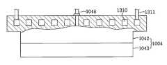
도 18에서는 기재를 생략하고 있지만, 가스 샤워헤드(1004)는 냉각 수단을 구비하고 있다. 이 냉각 수단은 구체적으로는 예를 들면 도 25a 및 도 25b에 나타내는 바와 같이, 전극부(1042)의 내부에 있어서 처리 가스 공급로(1045)와 간섭하지 않도록 나선상으로 수평방향으로 둘러 형성된 온도 조절 유로(1310)이다. 이 온도 조절 유로(1310)내를 소정의 온도로 조절된 온도 조절 매체 예를 들면 물이 온도 조절 유체 통유로(1311)를 거쳐서 통류하는 것에 의해, 해당 가스 샤워헤드(4)의 온도 조절이 가능하도록 구성되어 있다. 또한, 도 25a는 도 25b에 있어서의 A-A선으로 가스 샤워헤드(4)를 절단한 종단면도에 상당하고 있다.Although the base material is abbreviate | omitted in FIG. 18, the
또한, 도 26에도 나타내는 바와 같이, 해당 플라즈마 에칭 처리 장치에는 제어부(1007)가 접속되어 있다. 이 제어부(1007)는 CPU(1011), 프로그램(을 기억한 프로그램 기억부)(1012), 작업용의 워크 메모리(1013), 및 데이터 기억부인 메모리(1014)를 구비하고 있다. 메모리(1014)에는 각 레시피마다 에칭 처리를 실행하는 막(피에칭막)의 종류, 에칭 가스의 종류, 가스 유량, 처리 압력, 가스 샤워헤드(1004)의 온도, 각각의 안테나 모듈(1071)에 공급하는 마이크로파의 전력의 크기의 값, 직류 전원(1053)에 인가하는 부의 직류 전압의 값 등의 처리 조건이 기입되는 영역이 마련되어 있다.26, the
후술하는 바와 같이, 웨이퍼(W)상에는 서로 종류가 다른 다층의 막이 적층되어 있다. 그 때문에, 이 다층막에 대해 에칭 처리를 실행하는 경우에는 각각의 막마다 에칭 가스의 종류가 다르고, 또한 각각의 막마다 에칭 가스의 유량이나 처리 압력 등도 다르다. 따라서, 웨이퍼(W)의 면내에 있어서 균일하게 에칭 처리를 실행하기 위해서는 각각의 막마다 면내에 있어서 에칭 가스를 균일하게 플라즈마화할 필요가 있다. 특히, 웨이퍼(W)의 직경방향에 있어서 균일한 플라즈마를 형성할 필요가 있다. 그래서, 본 실시형태에서는 가스 샤워헤드(1004)에 인가하는 부의 직류 전압의 크기를 조정하는 것에 의해서, 안테나 모듈(1071)에 의해 처리 영역의 둘레가장자리부에 형성되는 전계의 강도와, 해당 부의 직류 전압에 의해 처리 영역의 중앙부측에 인입하는 전계의 강도를 각각의 막마다 조정하여, 이 전계에 의해 형성되는 플라즈마의 양(농도)을 면내에 있어서 균일화하도록 하고 있다.As will be described later, on the wafer W, multilayer films of different types are stacked. Therefore, when performing an etching process with respect to this multilayer film, the kind of etching gas differs for every film | membrane, and the flow volume of a etching gas, processing pressure, etc. differ for each film | membrane. Therefore, in order to perform the etching process uniformly in the surface of the wafer W, it is necessary to uniformly plasmamize the etching gas in the surface for each film. In particular, it is necessary to form a uniform plasma in the radial direction of the wafer (W). Therefore, in this embodiment, by adjusting the magnitude of the DC voltage of the part applied to the
또한, 예를 들면, 가변 이득 앰프(1076)에 의해 각각의 안테나 모듈(1071)에 공급하는 마이크로파의 전력의 크기를 각각의 막마다 조정하는 것에 의해서, 마이크로파의 전계에 의해 형성되는 플라즈마의 양을 둘레방향에 있어서도 균일화할 수 있다. 즉, 본 실시형태에서는 각각의 막마다 웨이퍼(W)의 면내(직경방향 및 둘레방향)에 있어서 플라즈마의 양을 균일화할 수 있다. 그 때문에, 예를 들면 실험이나 계산을 실행해서, 각각의 막(레시피)마다 가스 샤워헤드(1004)에 인가해야 할 전압의 값, 및 각각의 안테나 모듈(1071)에 공급해야 할 마이크로파의 전력의 크기를 미리 구해 두고, 이들 값을 각각의 레시피마다 기억하도록 하고 있다. 또한, 이와 같이 레시피마다 미리 이들 값을 구해 두지 않아도, 예를 들면 처리를 실행할 때마다, 해당 값을 계산해서 구하도록 해도 좋다. 또한, 안테나 모듈(1071)에 공급하는 마이크로파의 전력의 크기를, 복수의 레시피에 있어서 공통화하여 부의 직류 전압의 크기만을 레시피마다 변경하도록 해도 좋다.For example, the amount of plasma formed by the electric field of the microwave is adjusted by adjusting the magnitude of the microwave power supplied to each
상기의 프로그램(1012)은 에칭 처리를 실행하는 막마다 CPU(1011)를 거쳐서 메모리(1014)로부터 기술한 레시피를 작업용의 워크 메모리(1013)에 읽어내어, 이 레시피에 따라서, 플라즈마 처리 장치의 각 부에 제어 신호를 보내고, 후술하는 각 스텝을 진행시킴으로써 에칭 처리를 실행하는 바와 같이 명령이 내장되어 있다. 이 프로그램(처리 파라미터의 입력 조작이나 표시에 관한 프로그램도 포함)(1012)은 예를 들면 하드 디스크, 컴팩트 디스크, 마그네트 옵티컬 디스크, 메모리카드 등의 기억 매체(1008)에 저장되어, 해당 기억부(1008)로부터 제어부(1007)(의 프로그램 기억부(1012))에 인스톨되는 것이 일반적이다.The program 1012 reads the recipe described from the
다음에, 상기의 플라즈마 처리 장치의 작용에 대해, 도 27 내지 도 31을 참조해서 설명한다.Next, the operation of the plasma processing apparatus will be described with reference to FIGS. 27 to 31.
여기서, 피처리기판인 반도체 웨이퍼(이하「웨이퍼」라 함) W에 대해 간단히 설명하면, 해당 웨이퍼(W)는 예를 들면 소정의 패턴이 패터닝된 포토 레지스트 마스크, 예를 들면 유기물로 이루어지는 반사 방지막, 아몰퍼스 카본막, 절연막(SiO2막이나 SiCOH막) 혹은 Poly-Si(다결정 실리콘)막 및, 예를 들면 무기막으로 이루어지는 에칭 정지막 등으로 이루어지는 적층막이 상측부터 이 순서로 실리콘막 상에 적층되어 있다.Here, the semiconductor wafer (hereinafter referred to as "wafer") W, which is the substrate to be processed, will be briefly described. The wafer W is, for example, a photoresist mask patterned with a predetermined pattern, for example, an antireflection film made of an organic material. , A lamination film made of an amorphous carbon film, an insulating film (SiO2 film or SiCOH film) or a Poly-Si (polycrystalline silicon) film, and an etching stop film made of, for example, an inorganic film, is laminated on the silicon film in this order from above. It is.
우선, 웨이퍼(W)의 표면에 형성된 피에칭막에 따른 레시피가, 메모리(1014)로부터 워크 메모리(1013)에 읽어내어진다. 이 예에 있어서는 기술한 바와 같이, 표층의 피에칭이 예를 들면 반사 방지막이기 때문에, 이 막에 따른 레시피가 읽어내어진다. 그리고, 진공 분위기에 유지된 진공 반송실로부터 기판 반송 수단(모두 도시하지 않음)에 의해 처리 용기(1021)내에 웨이퍼(W)가 반입되어, 탑재대(1003)에 탑재된 후, 게이트밸브(1026)가 닫힌다. 그리고, 진공 배기 수단(1023)에 의해 처리 용기(1021)내가 예를 들면 압력 조정 밸브(1024a)가 완전 개방으로 된 상태로 되는 동시에, 온도 조절 유로(1037) 및 가스 유로(1038)로부터 소정의 온도로 조절된 온도 조절 매체 및 백사이드 가스가 공급되어, 웨이퍼(W)가 소정의 온도로 조정된다. 또한, 온도 조절 유체 통유로(1311)로부터 소정의 온도로 조절된 온도 조절 매체를 온도 조절 유로(1310)내에 통류시키는 것에 의해, 가스 샤워헤드(1004)가 소정의 온도로 조절된다.First, a recipe corresponding to the etching target film formed on the surface of the wafer W is read from the
계속해서, 마이크로파 출력부(1080)로부터 안테나 모듈(1071)을 향해 소정 전력의 마이크로파 예를 들면 주파수가 2.45㎓, 전력이 0∼4000W의 마이크로파를 공급하는 동시에, 탑재대(1003)에 고주파 전원(1031a)으로부터 바이어스용의 고주파를 공급한다. 마이크로파 출력부(1080)의 마이크로파 발진기(1082)로부터 발진되는 마이크로파는 앰프(1083)에서 증폭된 후, 분배기(1084)에 의해 각각의 안테나 모듈(1071)에 분배된다. 그리고, 안테나 모듈(1071)에서는 마이크로파는 가변 이득 앰프(1076) 및 메인 앰프(1077)에서 각각의 안테나 모듈(1071)마다 개별적으로 증폭되고, 다음에 2개의 마이크로 스트립 라인(1116, 1116)으로부터 출력되어 합성된 후, 평면 슬롯 안테나(1101)를 거쳐서 처리 용기(1021)내에 공급되게 된다.Subsequently, a microwave having a predetermined power, for example, a frequency of 2.45 GHz and a power of 0 to 4000 W, is supplied from the
안테나 모듈(1071)에 마이크로파를 공급하고, 도 23에 나타내는 바와 같은 슬롯 배치를 채용하는 것에 의해, 가스 샤워헤드(1004)의 아래쪽 공간을 둘러싸는 영역에, 외측 천판(1060)을 거쳐서 둘레방향에 걸쳐 웨이퍼(W)의 직경방향으로 수평인(처리 영역의 둘레가장자리부측에서 가스 샤워헤드(1004)의 중심방향을 향하고, 및 중심방향에서 둘레가장자리부측을 향하는) 전계 Er이 형성된다. 그리고, 가스 샤워헤드(1004)에 소정 크기의 부의 예를 들면 -500V의 직류 전압이 인가된다. 이 부의 직류 전압에 의해, 해당 가스 샤워헤드(1004)의 하면에 근접하는 위치에 부의 전계가 형성된다.By supplying microwaves to the
다음에, 처리 가스 공급계(1049)로부터 처리 용기(1021)내에 에칭 가스와 함께 예를 들면 Ar 가스가 공급되어, 처리 용기(1021)내가 소정의 압력 예를 들면 5.3Pa(40mTorr)로 조정된다. Ar 가스는 저에너지로 활성화되기 때문에, 에칭 가스와 함께 처리 용기(1021)내에 공급되는 것이 바람직하다. 이들 에칭 가스와 Ar 가스의 혼합 가스인 처리 가스는 처리 용기(1021)내로 확산해 가고, 기술한 전계 Er에 의해, 안테나 모듈(1071)의 아래쪽 위치에 있어서 플라즈마화되어, Ar+이온이나 에칭 가스 재료의 이온 및 전자 등을 포함하는 플라즈마가 생성된다. 그리고, 처리 영역의 둘레가장자리부측에 있어서 생성된 플라즈마는 처리 용기(1021)내, 예를 들면 가스 샤워헤드(4)의 중앙부측으로 확산해 간다. 이 플라즈마에 의해, 해당 중앙부측의 가스도 플라즈마화된다. 이것에 의해, 처리 영역에서는 수평방향의 전체에 걸쳐 플라즈마(1080)가 생성되게 된다. 여기서, 가스 샤워헤드(1004)에 부의 직류 전압을 인가하지 않으면, 도 27에 나타내는 바와 같이, 주로 안테나 모듈(1071)의 아래쪽위치에 있어서만 플라즈마가 생성되고, 중앙부측의 플라즈마 밀도가 둘레가장자리부측보다도 얇게 되어 버린다. 도 27에 있어서, 플라즈마 밀도가 높은 영역에 사선이 그어져 있다.Next, for example, Ar gas is supplied from the processing
그러나, 본 실시형태에서는 기술한 바와 같이, 가스 샤워헤드(1004)에 부의 직류 전압이 인가되므로, 가스 샤워헤드(1004)의 하면에 근접하는 영역에 부의 전계가 형성된다. 따라서, 이 바로 아래에 두꺼운 DC 시스(1001)가 형성된다. 이 DC 시스(1001)는 부의 직류 전압의 크기에 따른 두께로 된다. 그리고, 도 28에 나타내는 바와 같이, 전계 Er이 가스 샤워헤드(1004)의 중앙부측을 향해 DC 시스(1001)내를 침투해 가므로, 이것에 의거하여, 웨이퍼(W)의 면내에 걸쳐 균일성이 높은 플라즈마가 생성된다. 그 이유에 대해서는 다음과 같이 추측할 수 있다.However, in the present embodiment, as described above, since a negative direct current voltage is applied to the
즉, DC 시스(1001)에 의해, 가스 샤워헤드(1004)의 둘레가장자리의 전계 Er이 중앙부측에 강하게 끌어당겨지므로, 가스 샤워헤드(1004)의 아래쪽위치에 있어서도 강도가 강한 전계가 형성된다. 그 때문에, 가스 샤워헤드(1004)로부터 토출되는 처리 가스는 해당 가스 샤워헤드(1004)의 아래쪽에 끌어당겨진 전계에 의해, 순간적으로 플라즈마화된다. 한편, 이 전계에 의해서 처리 가스가 플라즈마화되지 않은 경우에도, 예를 들면 해당 처리 가스가 안테나 모듈(1071)의 아래쪽위치에 도달하면, 해당 아래쪽위치에 있어서의 강도한 강한 전계 Er에 의해서 플라즈마화되어 간다. 또한, 플라즈마화되지 않은 처리 가스가 예를 들면 DC 시스(1001)의 하단위치에 도달하면, 해당 DC 시스(1001)로부터 전계의 에너지를 흡수하는 것에 의해서, 플라즈마화되어 간다.That is, since the electric field Er of the peripheral edge of the
그리고, 이 플라즈마(1002)가 아래쪽으로 통류하고, 예를 들면 플라즈마(1002) 중의 전자가 처리 가스에 충돌하면, 해당 처리 가스가 플라즈마화된다. 또한, 이 플라즈마화에 의해 생성된 전자가 순차 처리 가스에 충돌해가는 것에 의해서, 도 29에 나타내는 바와 같이, 순차 플라즈마화가 진행하여, 플라즈마(1002)가 고밀도화되어 간다. 이와 같이 해서, 안테나 모듈(1071)에 의해 생성된 전계 Er이 소위 DC 시스(1001)를 거쳐서 가스 샤워헤드(1004)의 아래쪽측으로 넓어져 가는 동시에, 이 전계에 의해 형성된 플라즈마(1002)가 아래쪽측을 향하는 배기류를 타고 웨이퍼(W)상으로 하강해서, 웨이퍼(W)의 면내(직경방향 및 둘레방향)에 걸쳐 균일성이 높은 플라즈마(1002)가 형성되게 된다.When the
또한, 도 30에 나타내는 바와 같이, 플라즈마 중의 플러스의 이온, 예를 들면 상기의 Ar+이온이 DC 시스(1001)의 부의 전계에 강하게 끌어당겨져 가스 샤워헤드(1004)에 충돌하고, 이 충돌에 의해, 가스 샤워헤드(1004)로부터 2차 전자가 발생하여, DC 시스(1001)내에 있어서 이 2차 전자가 가속되어 아래쪽측으로 튀어나가고, 이 2차 전자에 의해 처리 가스가 플라즈마화된다고 하는 효과도 있다. 이 때문에, 웨이퍼(W)의 위쪽의 플라즈마(1002)는 밀도가 더욱 높아지고, 또한, 면내에 있어서 더욱 균일화되어 가게 된다.As shown in FIG. 30, positive ions in the plasma, for example, Ar+ ions, are strongly attracted to the negative electric field of the
그리고, 도 31에 나타내는 바와 같이, 플라즈마중의 이온이 고주파 전원(1031a)에 의한 고주파 바이어스에 의해서 웨이퍼(W)측에 끌어당겨짐으로써 수직성이 높은 에칭 처리가 진행해 가게 된다. 이와 같이 해서, 반사 방지막의 하층의 아몰퍼스 카본막이 노출될 때까지, 해당 반사 방지막의 에칭 처리가 실행된다.And as shown in FIG. 31, the etching process with high perpendicularity advances because the ion in plasma is attracted to the wafer W side by the high frequency bias by the high
그 후, 처리 가스의 공급이 정지되는 동시에, 안테나 모듈(1071)에의 마이크로파의 공급과 가스 샤워헤드(1004)에의 부의 직류 전압의 인가가 정지된다. 그리고, 처리 용기(1021)내가 진공 배기되어, 계속해서 에칭 처리를 실행하는 막인 아몰퍼스 카본막에 따른 레시피가 메모리(1014)로부터 읽어내어지고, 이 아몰퍼스 카본막의 에칭 처리가 시작된다. 그 후, 아몰퍼스 카본막의 하층측의 막에 대해, 마찬가지로 순차 레시피가 읽어내어져, 에칭 처리가 실행되어 간다.Thereafter, the supply of the processing gas is stopped, and the supply of the microwave to the
상술한 실시형태에 의하면, 처리 용기(1021)의 천벽의 중앙부에 도전성 부재로 이루어지는 가스 샤워헤드(1004)가 마련되어, 웨이퍼(W)에 대해 면내 균일성이 높다고 하는 형태로 가스의 공급이 실행되는 한편, 가스 샤워헤드(1004)의 아래쪽 공간을 둘러싸는 영역에 복수의 안테나 모듈(1071)에 의해 둘레방향에 걸쳐 균일한 플라즈마가 발생되고, 또한, 가스 샤워헤드(1004)에 부의 직류 전압을 인가함으로써 그 아래쪽에 DC 시스(1001)가 형성되고, 해당 DC 시스(1001)를 거쳐서 상기 플라즈마(1002)가 중앙부측으로 확대되도록 되어 있다. 따라서, 마이크로파를 이용하는 형태이면서, 가스 샤워헤드(1004)를 이용하여 균일성이 높은 가스의 공급을 실행할 수 있고, 또한, 가스 샤워헤드(1004)의 아래쪽측 공간도 포함시켜 웨이퍼(W)의 면을 따라 균일성이 높은 플라즈마(1002)를 발생시킬 수 있다. 이 때문에, 웨이퍼(W)에 대해 면내 균일성이 높은 플라즈마 처리, 이 예에서는 에칭 처리를 실현할 수 있다.According to the above-mentioned embodiment, the
그리고, 가스 샤워헤드(1004)에 인가하는 부의 직류 전압에 의해 DC 시스(1001)의 두께를 조정하는 것에 의해서, 또한, 각각의 안테나 모듈(1071)에 공급하는 마이크로파의 전력을 조정하는 것에 의해서, 처리 레시피에 따른 면내 균일성이 높은 적절한 플라즈마(1002)를 용이하게 얻을 수 있다. 마이크로파를 이용한 플라즈마(1002)는 이 플라즈마 처리 장치와 같이, 처리 용기(1021)의 천판(외측 천판(1060))의 위에 안테나 모듈(1071)을 마련하는 것만으로 발생시킬 수 있으므로, 장치 구성이 간이하고 비용적으로 유리하다. 한편, 종래의 방식은 면적이 큰 기판에 대해, 가스의 공급 등의 점에서 불리하다고 되고 있었지만, 본 실시형태의 플라즈마 처리 장치에서는 그러한 불리가 없다.And by adjusting the thickness of the
또한, 상술한 장치는 Ar+이온의 충격에 의해서, 소위 스퍼터와 같이 가스 샤워헤드(1004)가 물리적으로 깎여 버리는 것도 고려지만, 가스 샤워헤드(1004)의 하면이 실리콘으로 구성되어 있으므로, 오염의 우려가 없다. 또한, 가스 샤워헤드(1004)로부터 균일하게 에칭 가스가 공급되므로, 해당 가스 샤워헤드(1004)와 탑재대(1003)를 근접시킬 수 있고, 처리 용기(1021)의 높이를 억제할 수 있다. 또한, 지지 부재(1043)에 온도 조절 유로(1310)를 둘러 형성하는 것에 의해, 레시피에 따라 가스 샤워헤드(1004)의 온도를 조정할 수 있다.In addition, the above-described apparatus considers that the
또한, 상기의 예에 있어서는 안테나 모듈(1071)을 외측 천판(1060)의 위쪽에 설치하도록 했지만, 도 32에 나타내는 바와 같이, 외측 천판(1060)에 둘레방향에 걸쳐 등간격으로 복수 개소, 예를 들면 8개소에 예를 들면 원형의 개구부(1120)를 형성하고, 이 개구부(1120)내에 안테나 모듈(1071)을 기밀하게 매설하도록 해도 좋다. 이 경우에는 예를 들면 개구부(1120)의 상단측을 하단측보다도 한층 크게 잘라내는 것에 의해서, 해당 하단측에 환상의 걸어맞춤 단부(1121)를 형성하고, 예를 들면 O-링 등을 거쳐서, 이 걸어맞춤 단부(1121)의 단면과 안테나 모듈(1071)의 하단의 둘레가장자리인 피걸어맞춤면을 걸어맞춰 안테나 모듈(1071)을 기밀하게 유지해도 좋다. 이와 같은 구성의 플라즈마 에칭 처리 장치에 있어서도, 상기의 예와 마찬가지로 면내에 걸쳐 플라즈마가 균일하게 형성되고, 마찬가지의 효과가 얻어진다.In the above example, the
이 때, 안테나 모듈(1071)의 아래쪽측의 영역과 처리 영역이 연통하고 있기 때문에, 예를 들면 외측 천판(1060)을 금속 예를 들면 알루미늄에 의해 구성해도 좋다. 또한, 외측 천판(1060)의 아래쪽 위치에 있어서의 처리 용기(1021)내에 안테나 모듈(1071)을 설치하도록 해도 좋다. 이 경우에도, 외측 천판(1060)을 예를 들면 도전성 부재 예를 들면 금속에 의해 구성해도 좋다. 이들 예와 같이 외측 천판(1060)을 도전성 부재에 의해 구성하는 경우에는 외측 천판(1060)과 가스 샤워헤드(1004) 사이에 절연 부재를 개재시키는 것이 바람직하다.At this time, since the area on the lower side of the
또한, 도시를 생략하지만, 외측 천판(1060)을 상측부분과 유전체로 이루어지는 하측부분으로 이루어지는 분할 구조체로서 구성하는 동시에, 이 하측부분에 예를 들면 둘레방향에 복수의 오목부를 등간격으로 형성하여, 이 오목부내에 안테나 모듈(1071)을 수납해도 좋다. 이 경우에 있어서도, 상기의 예와 마찬가지의 작용이 얻어지고, 즉, 에칭 가스가 균일하게 플라즈마화되어 면내에 있어서 균일하게 에칭 처리가 실행되게 된다.Although not shown, the outer
상기의 예에 있어서는 가스 샤워헤드(1004)에 인가하는 부의 직류 전압의 값을 조정하여, 직경방향에 있어서의 플라즈마 밀도를 균일화하도록 했지만, 이 부의 직류 전압을 소정의 값으로 고정시켜 안테나 모듈(1071)에 공급하는 마이크로파의 전력의 크기를 조정하여, 직경방향에 있어서의 플라즈마 밀도를 균일화하도록 해도 좋다. 또한, 상기의 예에서는 각각의 안테나 모듈(1071)에 공급하는 마이크로파의 전력을 둘레방향에 걸쳐 조정하여, 둘레방향에 있어서의 플라즈마의 양에 대해서도 균일화하도록 했지만, 예를 들면 둘레방향에 있어서의 플라즈마의 양의 편차가 극히 작은 경우에는 각각의 안테나 모듈(1071)에 동일한 전력의 마이크로파를 공급해도 좋다. 또한, 둘레방향에 있어서의 플라즈마(1002)의 농도를 균일화함에 있어서, 마이크로파의 위상을 조정해도 좋고, 마이크로파의 위상과 함께 마이크로파의 전력의 크기를 조정해도 좋다.In the above example, the value of the negative DC voltage applied to the
또한, 상기의 예에 있어서는 둘레방향에 걸쳐 복수 개소에 안테나 모듈(1071)을 마련하도록 했지만, 예를 들면 처리 용기(1021)의 천벽(가스 샤워헤드(1004) 및 외측 천판(1060))의 위쪽을 덮도록 마이크로파 공급부로서 안테나부(1200)를 마련하도록 해도 좋다. 이러한 예에 대해, 도 33 및 도 34를 참조해서 설명한다. 또한, 기술한 도 18에 나타내는 플라즈마 에칭 처리 장치와 동일한 구성의 부재에 대해서는 동일 부호를 붙이고 설명을 생략한다.In addition, in the above example, although the
이 안테나부(1200)는 예를 들면 두께가 1㎜ 정도의 동판으로 구성되고, 평면형상이 원형이고 하면측이 원형으로 개구된 편평한 안테나 본체(1201)와, 이 안테나 본체(1201)의 하면측의 개구부를 막도록 마련되고, 예를 들면 원 편파를 발생시키기 위한 다수의 슬롯(1202)이 형성된 평면 안테나 부재(슬롯판)(1203)를 구비하고 있다. 이들 안테나 본체(1201)와 슬롯 부재(1203)는 도체로 이루어지고, 편평한 원형 도파관을 구성하고 있다. 그리고, 평면 안테나 부재(1203)의 하면은 처리 용기(1021)의 상면(가스 샤워헤드(1004) 및 외측 천판(1060))에 밀접되어 있다.The
상기의 슬롯(1202)은 도 34에 나타내는 바와 같이, 대략 T자형상으로 약간 이간시켜 배치된 한 쌍의 슬롯(1202a, 1202b)을 1조로 해서, 둘레방향을 따라 예를 들면 동심원형상이나 소용돌이형상으로 형성되어 있다. 슬롯(1202a)과 슬롯(1202b)을 서로 대략 직교하는 바와 같은 관계로 배열하고 있으므로, 2개의 직교하는 편파성분을 포함하는 원 편파가 방사되게 된다. 이 때, 슬롯 쌍(1202a, 1202b)을, 후술하는 지상판(遲相板)(1204)에 의해 압축된 마이크로파의 파장에 대응한 간격으로 배열하는 것에 의해, 마이크로파가 평면 안테나 부재(1203)로부터 대략 평면파로서 방사된다.As shown in Fig. 34, the
평면 안테나 부재(1203)와 안테나 본체(1201) 사이에는 상기 원형 도파관내의 마이크로파의 파장을 짧게 하기 위해, 예를 들면 산화 알루미늄(Al2O3)이나 질화 규소(Si3N4) 등의 저손실 유전체 재료에 의해 구성된 지상판(1204)이 개재되어 있다. 이들 안테나 본체(1201), 평면 안테나 부재(1203) 및 지상판(1204)에 의해, 레이디얼 라인 슬롯 안테나(Radial Line Slot Antenna)가 구성되어 있다.A low loss dielectric such as, for example, aluminum oxide (Al2 O3 ) or silicon nitride (Si3 N4 ) in order to shorten the wavelength of the microwaves in the circular waveguide between the
안테나부(1200)의 상면에는 동축 도파관(1205)을 거쳐서, 마이크로파 발생 수단(1206)이 접속되어 있다. 이것에 의해, 안테나부(1200)에 예를 들면 주파수가 2.45㎓ 혹은 8.3㎓의 마이크로파가 공급되도록 되어 있다. 동축 도파관(1205)은 외측의 도파관(1206A)과 내측의 중심 도체(1206B)에 의해 구성되어 있고, 도파관(1206A)은 안테나 본체(1201)에 접속되며, 중심 도체(1206B)는 지상판(1204)에 형성된 개구부를 거쳐서 평면 안테나 부재(1203)에 접속되어 있다.The microwave generating means 1206 is connected to the upper surface of the
이 플라즈마 에칭 처리 장치에서는 마이크로파 발생 수단(1206)으로부터 예를 들면 2.45㎓, 500∼3000W의 마이크로파가 공급되면, 이 마이크로파가 TM모드 혹은 TE모드 혹은 TEM모드로 동축 도파관(1205)내를 전파해서, 안테나부(1200)의 평면 안테나 부재(1203)에 도달하고, 도 35에 나타내는 바와 같이, 평면 안테나 부재(1203)의 중심부에서 둘레가장자리영역을 향해 방사상으로 전파되는 동시에, 슬롯 쌍(1202a, 1202b)으로부터 외측 천판(1060)을 거쳐서 처리 용기(1021)내를 향해 방출된다. 그 때문에, 가스 샤워헤드(1004)의 아래쪽 공간을 둘러싸는 둘레가장자리영역에, 둘레방향에 걸쳐 균일한 전계 Er이 형성된다. 그리고, 기술한 예와 마찬가지로, 직류 전원(1053)에 예를 들면 0∼-2000V의 부의 직류 전압을 인가하는 것에 의해, 상기 전계 Er이 가스 샤워헤드(1004)의 아래쪽에 형성된 DC 시스(1001)에 강하게 끌어당겨져 기술한 예와 마찬가지로 면내(둘레방향 및 직경방향)에 걸쳐 플라즈마가 균일하게 형성되고, 수직성이 높은 에칭 처리가 진행해 가게 된다. 그 때문에, 이 플라즈마 에칭 처리 장치에 있어서도, 기술한 예와 마찬가지의 효과가 얻어진다.In the plasma etching processing apparatus, when microwaves of, for example, 2.45 kHz and 500 to 3000 W are supplied from the microwave generating means 1206, the microwaves propagate in the
이 경우에 있어서도, 기술한 도 32에 나타낸 바와 같이, 외측 천판(1060)에 둘레방향에 걸쳐 개구부(1120)를 형성하도록 해도 좋고, 또는 외측 천판(1060)을 마련하지 않고 소위 가스 샤워헤드(1004)를 둘러싸도록 링형상의 개구부를 형성하고, 안테나부(1200)에 가스 샤워헤드(1004)를 고정시키는 동시에, 안테나 본체(1201)의 하면의 둘레가장자리와 처리 용기(1021)의 상면의 둘레가장자리를 기밀하게 접촉시키는 것이어도 좋다. 여기서, 가스 샤워헤드(1004)에 있어서, 처리 영역측의 샤워 플레이트(지지 부재(1043))만을 도전성 부재에 의해 구성하고, 이 샤워 플레이트와 직류 전원(1053)을 도전로로 접속해서 샤워 플레이트에 부의 전압을 인가한다고 하는 형태도, 본 발명의 기술범위에 포함된다.Also in this case, as shown in FIG. 32 described above, the
상기의 각 예에 있어서는 플라즈마 처리로서 에칭 처리를 예로 들어 설명했지만, 본 발명의 플라즈마 처리 장치를 예를 들면 플라즈마를 이용한 CVD(Chemical Vapor Deposition)법을 이용한 성막 처리 장치에 적용해도 좋고, 애싱 장치에 적용해도 좋다. 예를 들면 성막 장치에 있어서는 성막 가스의 종류나 유량, 압력 등의 처리 조건에 따라, 가스 샤워헤드(4)에 인가되는 부의 직류 전압의 크기가 조정되어, 면내에 있어서 균일한 성막속도로 성막처리가 실행되게 된다.In each of the above examples, the etching treatment is described as an example of the plasma treatment. However, the plasma processing apparatus of the present invention may be applied to a film forming apparatus using, for example, a CVD (Chemical Vapor Deposition) method using plasma. You may apply. For example, in the film forming apparatus, the magnitude of the negative DC voltage applied to the
(시뮬레이션)(simulation)
기술한 도 35에 나타내는 바와 같이 안테나 모듈(1071)을 설치하는 동시에, 가스 샤워헤드(1004)에 부의 직류 전압을 인가했을 때에, 처리 용기(1021)내에 형성되는 전계 Er(TM모드의 전계)의 밀도분포가 어떻게 변화되는지 확인하기 위해, 전자계 계산 소프트인 COMSOL을 이용하여, 시뮬레이션(계산)을 실행하였다.As shown in FIG. 35 described above, when the
안테나 모듈(1071)에 1.8㎓, 2000W의 마이크로파를 공급하는 경우에 대해 계산이 실행되었다. 또한, 가스 샤워헤드(1004)에 부의 직류 전압을 인가하는 것에 의해, 가스 샤워헤드(1004)의 아래쪽측에 형성되는 DC 시스(1001)의 두께가 1㎜, 5㎜, 10㎜로 되는 경우에 대해 각각 계산을 실행하였다. 그리고, 처리 용기(1021)의 중앙부로부터 우측절반에 대해, 플라즈마(처리 가스)에 흡수되는 전계 강도를 조사하였다. 이 흡수 전계 강도에 의해서, DC 시스(1001)의 아래쪽측의 플라즈마의 전자 밀도를 평가할 수 있다.The calculation was performed for the case of supplying 1.8 GHz and 2000 W of microwaves to the
(결과)(result)
도 36의 (a), (b)에 나타내는 바와 같이, DC 시스(1001)의 두께가 1㎜에서 5㎜로 증가하는 것에 의해서, DC 시스(1001)의 아래쪽측에 있어서의 흡수 전계 강도가 처리 용기(1021)의 중앙부측까지 크게 되어 있다. 이것으로부터, 전계 Er이 웨이퍼(W)의 중앙부측을 향해 길게 신장하여, 면내에 있어서의 플라즈마 밀도가 균일화되는 것을 알 수 있었다. 또한, 도 36의 (c)에 나타내는 바와 같이, DC 시스(1001)의 두께를 증가시켜 가는 것에 의해, 즉 가스 샤워헤드(1004)에 인가하는 부의 직류 전압을 크게 해 가는 것에 의해, 안테나 모듈(1071)의 아래쪽측에 형성되는 전계 Er이 웨이퍼(W)의 중앙부측을 향해 또한 끌어당겨져 신장해 가는 것을 알 수 있었다.As shown to Fig.36 (a), (b), when the thickness of the
Claims (20)
Translated fromKorean처리 용기와,
상기 처리 용기내에 마련되고 기판을 탑재하기 위한 탑재대와,
상기 탑재대에 대향하도록 마련되고, 상기 처리 용기내에 처리 가스를 공급하기 위한 다수의 가스 토출 구멍이 그 하면에 형성된 도전성 부재로 이루어지는 가스 샤워헤드와,
상기 가스 샤워헤드의 아래쪽 공간을 둘러싸는 영역에 유도 결합형 플라즈마를 발생시키기 위해 고주파 전류가 공급되는 유도 코일과,
상기 가스 샤워헤드에 부의 직류 전압을 인가하여, 상기 유도 코일에 의해 유도되는 전계를 처리 영역의 중앙부측에 인입하기 위한 부전압 공급 수단과,
상기 처리 용기내를 진공 배기하기 위한 수단을 구비한 것을 특징으로 하는
플라즈마 처리 장치.In the plasma processing apparatus which performs a process with a plasma with respect to a board | substrate,
Processing container,
A mounting table provided in the processing container for mounting a substrate;
A gas shower head provided to face the mounting table, the gas shower head comprising a conductive member formed on a lower surface of the gas discharge holes for supplying a processing gas into the processing container;
An induction coil supplied with a high frequency current to generate an inductively coupled plasma in an area surrounding a space below the gas shower head;
Negative voltage supply means for applying a negative DC voltage to the gas shower head to introduce an electric field induced by the induction coil to the center portion of the processing region;
Means for evacuating the interior of the processing vessel;
Plasma processing apparatus.
상기 유도 코일은 기판과 평행하고 또한 상기 처리 용기의 직경방향과 교차하는 방향으로 신장하는 축의 주위에 감겨 있는 것을 특징으로 하는
플라즈마 처리 장치.The method of claim 1,
The induction coil is wound around an axis parallel to the substrate and extending in a direction crossing the radial direction of the processing container.
Plasma processing apparatus.
상기 유도 코일은 처리 용기의 둘레방향을 따라 복수 배치되어 있는 것을 특징으로 하는
플라즈마 처리 장치.3. The method according to claim 1 or 2,
The induction coil is disposed in a plurality along the circumferential direction of the processing container, characterized in that
Plasma processing apparatus.
상기 유도 코일은 그 1변이 기판과 평행하게 되도록 각형으로 감겨 있는 것을 특징으로 하는
플라즈마 처리 장치.3. The method according to claim 1 or 2,
The induction coil is wound in a square so that one side thereof is parallel to the substrate.
Plasma processing apparatus.
상기 유도 코일은 상기 처리 용기보다도 위쪽측에 마련되고,
상기 가스 샤워헤드의 주위에 있어서의 상기 처리 용기의 천벽은 유전체로 형성되어 있는 것을 특징으로 하는
플라즈마 처리 장치.3. The method according to claim 1 or 2,
The induction coil is provided above the processing container,
A ceiling wall of the processing container around the gas shower head is formed of a dielectric.
Plasma processing apparatus.
상기 유도 코일은 유전체에 매설되어, 상기 처리 용기의 천벽의 일부를 구성하고 있는 것을 특징으로 하는
플라즈마 처리 장치.3. The method according to claim 1 or 2,
The induction coil is embedded in a dielectric and constitutes a part of the ceiling wall of the processing container.
Plasma processing apparatus.
상기 가스 샤워헤드의 적어도 하면측은 실리콘으로 형성되어 있는 것을 특징으로 하는
플라즈마 처리 장치.3. The method according to claim 1 or 2,
At least the lower surface side of the gas shower head is formed of silicon
Plasma processing apparatus.
기판에 대해 실행되는 처리의 레시피와, 상기 부의 직류 전압의 크기와, 유도 코일에 공급되는 고주파 전류의 크기를 대응지어 기억한 기억부와,
임의의 레시피에 따른 부의 직류 전압의 크기와 고주파 전류의 크기를 상기 기억부로부터 읽어내어 제어 신호를 출력하는 제어부를 더 구비한 것을 특징으로 하는
플라즈마 처리 장치.3. The method according to claim 1 or 2,
A storage unit which stores a recipe of a process performed on a substrate, a magnitude of the negative DC voltage and a magnitude of a high frequency current supplied to an induction coil,
And a control unit for reading the magnitude of the negative DC voltage and the high frequency current according to an arbitrary recipe from the storage unit and outputting a control signal.
Plasma processing apparatus.
처리 용기내의 탑재대 상에 기판을 탑재하는 공정과,
상기 탑재대에 대향하도록 마련된 도전성 부재로 이루어지는 가스 샤워헤드보다도 상기 처리 용기의 직경방향 외쪽측에 위치하는 유도 코일에 고주파 전류를 공급하는 것에 의해, 상기 가스 샤워헤드의 아래쪽측 공간을 둘러싸는 영역에 전계를 형성하는 공정과,
상기 가스 샤워헤드의 하면의 가스 토출 구멍으로부터 상기 처리 용기내에 처리 가스를 공급하여, 상기 전계에 의해 해당 처리 가스를 플라즈마화하는 공정과,
상기 가스 샤워헤드에 부의 직류 전압을 인가하고, 상기 유도 코일에 의해 유도된 전계를 처리 영역의 중앙부측에 인입하는 공정을 구비한 것을 특징으로 하는
플라즈마 처리 방법.In the plasma processing method of performing the processing by the plasma on the substrate,
Mounting a substrate on a mounting table in a processing container;
In a region surrounding the space below the gas shower head by supplying a high frequency current to the induction coil located on the radially outer side of the processing container rather than the gas shower head made of the conductive member provided to face the mounting table. Process of forming an electric field,
Supplying a processing gas into the processing container from a gas discharge hole in a lower surface of the gas shower head, and converting the processing gas into plasma by the electric field;
And applying a negative direct current voltage to the gas shower head, and drawing an electric field induced by the induction coil to the center side of the processing region.
Plasma treatment method.
상기 전계를 형성하는 공정은 기판과 평행하고 또한 상기 처리 용기의 직경방향과 교차하는 방향으로 신장하는 축의 주위에 감긴 유도 코일에 의해서 실행되는 것을 특징으로 하는
플라즈마 처리 방법.The method of claim 9,
The step of forming the electric field is performed by an induction coil wound around an axis parallel to the substrate and extending in a direction crossing the radial direction of the processing container.
Plasma treatment method.
상기 전계를 형성하는 공정은 처리 용기의 둘레방향을 따라 복수 배치된 유도 코일에 의해서 실행되는 것을 특징으로 하는
플라즈마 처리 방법.11. The method according to claim 9 or 10,
The step of forming the electric field is performed by an induction coil disposed in a plurality along the circumferential direction of the processing container
Plasma treatment method.
상기 전계를 형성하는 공정은 그 1변이 기판과 평행하게 되도록 각형으로 감긴 유도 코일에 의해서 실행되는 것을 특징으로 하는
플라즈마 처리 방법.11. The method according to claim 9 or 10,
The step of forming the electric field is performed by an induction coil wound in a square so that one side thereof is parallel to the substrate.
Plasma treatment method.
기판에 대해 실행되는 처리의 레시피와, 상기 부의 직류 전압의 크기와, 유도 코일에 공급되는 고주파 전류의 크기를 대응지어 기억한 기억부로부터, 임의의 레시피에 따른 부의 직류 전압의 크기와 고주파 전류의 크기를 읽어내는 공정을 더 구비한 것을 특징으로 하는
플라즈마 처리 방법.11. The method according to claim 9 or 10,
The size of the negative DC voltage according to an arbitrary recipe and the high-frequency current are determined from a storage unit which stores a recipe of a process performed on the substrate and the magnitude of the negative DC voltage and the magnitude of the high frequency current supplied to the induction coil. Further comprising a step of reading the size
Plasma treatment method.
처리 용기내에 마련되고, 기판을 탑재하기 위한 탑재대와,
이 탑재대에 대향하도록 마련되고, 상기 처리 용기내에 처리 가스를 공급하기 위한 다수의 가스 토출 구멍이 그 하면에 형성된 도전성 부재로 이루어지는 가스 샤워헤드와,
상기 가스 샤워헤드의 아래쪽 공간을 둘러싸는 영역에 있어서 처리 가스를 플라즈마화하기 위해 마이크로파가 공급되는 마이크로파 공급부와,
상기 가스 샤워헤드에 부의 직류 전압을 인가하여, 상기 마이크로파에 의해 형성되는 전계를 처리 영역의 중앙부측에 인입하기 위한 부전압 공급 수단과,
상기 처리 용기내를 진공 배기하기 위한 수단을 구비한 것을 특징으로 하는
플라즈마 처리 장치.In the plasma processing apparatus which performs a process with a plasma with respect to a board | substrate,
A mounting table provided in the processing container for mounting the substrate,
A gas shower head provided to face the mounting table, the gas shower head comprising a conductive member formed on a lower surface of the gas discharge holes for supplying a processing gas into the processing container;
A microwave supply unit to which microwaves are supplied to plasma process gas in a region surrounding a space below the gas shower head;
Negative voltage supply means for applying a negative DC voltage to the gas shower head to introduce an electric field formed by the microwaves into the center portion of the processing region;
Means for evacuating the interior of the processing vessel;
Plasma processing apparatus.
상기 마이크로파 공급부는 처리 용기의 둘레방향을 따라 복수 배치되어 있는 것을 특징으로 하는
플라즈마 처리 장치.15. The method of claim 14,
The microwave supply unit is disposed in a plurality along the circumferential direction of the processing container, characterized in that
Plasma processing apparatus.
상기 가스 샤워헤드의 주위에 있어서의 상기 처리 용기의 천벽은 유전체로 형성되고,
상기 마이크로파 공급부는 해당 천벽의 위쪽측에 마련되어 있는 것을 특징으로 하는
플라즈마 처리 장치.16. The method according to claim 14 or 15,
The top wall of the processing container around the gas shower head is formed of a dielectric material,
The microwave supply unit is provided on the upper side of the ceiling wall
Plasma processing apparatus.
상기 가스 샤워헤드의 주위에 있어서의 상기 마이크로파 공급부의 아래쪽의 상기 처리 용기의 천벽에는 개구부가 형성되고,
상기 마이크로파 공급부는 상기 개구부를 막도록 상기 처리 용기에 기밀하게 마련되어 있는 것을 특징으로 하는
플라즈마 처리 장치.16. The method according to claim 14 or 15,
Openings are formed in the top wall of the processing container below the microwave supply section around the gas shower head,
The microwave supply portion is provided in the processing container to be airtight so as to close the opening.
Plasma processing apparatus.
기판에 대해 실행되는 처리의 레시피와, 상기 부의 직류 전압의 크기를 대응지어 기억한 기억부와,
임의의 레시피에 따른 부의 직류 전압의 크기를 상기 기억부로부터 읽어내어 제어 신호를 출력하는 제어부를 구비한 것을 특징으로 하는
플라즈마 처리 장치.16. The method according to claim 14 or 15,
A storage unit which stores a recipe of processing to be performed on a substrate and a magnitude of the negative DC voltage in association with each other;
And a control unit for reading a magnitude of a negative DC voltage according to an arbitrary recipe from the storage unit and outputting a control signal.
Plasma processing apparatus.
기판에 대해 실행되는 처리의 레시피와, 상기 부의 직류 전압의 크기와, 상기 마이크로파 공급부에 공급되는 마이크로파의 전력의 크기를 대응지어 기억한 기억부와,
임의의 레시피에 따른 부의 직류 전압의 크기와 마이크로파의 전력의 크기를 상기 기억부로부터 읽어내어 제어 신호를 출력하는 제어부를 더 구비한 것을 특징으로 하는
플라즈마 처리 장치.16. The method according to claim 14 or 15,
A storage unit which stores a recipe of processing to be performed on a substrate, a magnitude of the negative DC voltage, and a magnitude of power of microwaves supplied to the microwave supply unit;
And a control unit which reads the magnitude of the negative DC voltage and the magnitude of the microwave power according to an arbitrary recipe from the storage unit and outputs a control signal.
Plasma processing apparatus.
상기 마이크로파 공급부는 처리 용기의 둘레방향을 따라 복수 배치되고 상기 기억부는 상기 복수의 마이크로파 공급부에 공급되는 마이크로파의 전력의 각각의 크기를 상기 레시피에 대응지어 기억하도록 되어 있고, 상기 제어부는 상기 레시피에 따라서, 상기 복수의 마이크로파 공급부에 공급되는 마이크로파의 전력의 각각의 크기를 읽어내어 제어 신호를 출력하도록 되어 있는 것을 특징으로 하는
플라즈마 처리 장치.The method of claim 19,
The microwave supply unit is arranged in plural along the circumferential direction of the processing container, and the storage unit is configured to store each magnitude of the power of the microwaves supplied to the plurality of microwave supply units in correspondence with the recipe, and the control unit according to the recipe And outputting a control signal by reading the magnitude of the power of the microwaves supplied to the plurality of microwave supply units.
Plasma processing apparatus.
Applications Claiming Priority (5)
| Application Number | Priority Date | Filing Date | Title |
|---|---|---|---|
| JP2008182058AJP5332362B2 (en) | 2008-07-11 | 2008-07-11 | Plasma processing apparatus, plasma processing method, and storage medium |
| JPJP-P-2008-182058 | 2008-07-11 | ||
| JP2008254377AJP5309847B2 (en) | 2008-09-30 | 2008-09-30 | Plasma processing equipment |
| JPJP-P-2008-254377 | 2008-09-30 | ||
| PCT/JP2009/062378WO2010004997A1 (en) | 2008-07-11 | 2009-07-07 | Plasma processing apparatus |
Publications (2)
| Publication Number | Publication Date |
|---|---|
| KR20110018431A KR20110018431A (en) | 2011-02-23 |
| KR101245430B1true KR101245430B1 (en) | 2013-03-19 |
Family
ID=41507110
Family Applications (1)
| Application Number | Title | Priority Date | Filing Date |
|---|---|---|---|
| KR1020117000747AExpired - Fee RelatedKR101245430B1 (en) | 2008-07-11 | 2009-07-07 | Plasma processing apparatus and plasma processing method |
Country Status (4)
| Country | Link |
|---|---|
| US (1) | US8419960B2 (en) |
| KR (1) | KR101245430B1 (en) |
| CN (1) | CN102089867B (en) |
| WO (1) | WO2010004997A1 (en) |
Families Citing this family (131)
| Publication number | Priority date | Publication date | Assignee | Title |
|---|---|---|---|---|
| JP5391659B2 (en)* | 2008-11-18 | 2014-01-15 | 東京エレクトロン株式会社 | Plasma processing equipment |
| GB201021870D0 (en)* | 2010-12-23 | 2011-02-02 | Element Six Ltd | A microwave plasma reactor for manufacturing synthetic diamond material |
| US10283321B2 (en) | 2011-01-18 | 2019-05-07 | Applied Materials, Inc. | Semiconductor processing system and methods using capacitively coupled plasma |
| JP5982129B2 (en)* | 2011-02-15 | 2016-08-31 | 東京エレクトロン株式会社 | Electrode and plasma processing apparatus |
| US8999856B2 (en) | 2011-03-14 | 2015-04-07 | Applied Materials, Inc. | Methods for etch of sin films |
| US9064815B2 (en) | 2011-03-14 | 2015-06-23 | Applied Materials, Inc. | Methods for etch of metal and metal-oxide films |
| JP5732941B2 (en)* | 2011-03-16 | 2015-06-10 | 東京エレクトロン株式会社 | Plasma etching apparatus and plasma etching method |
| US9543123B2 (en) | 2011-03-31 | 2017-01-10 | Tokyo Electronics Limited | Plasma processing apparatus and plasma generation antenna |
| JP5893865B2 (en)* | 2011-03-31 | 2016-03-23 | 東京エレクトロン株式会社 | Plasma processing apparatus and microwave introduction apparatus |
| US9111727B2 (en)* | 2011-09-30 | 2015-08-18 | Tokyo Electron Limited | Plasma tuning rods in microwave resonator plasma sources |
| US9728416B2 (en) | 2011-09-30 | 2017-08-08 | Tokyo Electron Limited | Plasma tuning rods in microwave resonator plasma sources |
| US8808496B2 (en)* | 2011-09-30 | 2014-08-19 | Tokyo Electron Limited | Plasma tuning rods in microwave processing systems |
| US9396955B2 (en) | 2011-09-30 | 2016-07-19 | Tokyo Electron Limited | Plasma tuning rods in microwave resonator processing systems |
| CN103187264A (en)* | 2011-12-28 | 2013-07-03 | 中微半导体设备(上海)有限公司 | A method for etching a silicon oxide layer in a plasma etching chamber |
| JP5973731B2 (en) | 2012-01-13 | 2016-08-23 | 東京エレクトロン株式会社 | Plasma processing apparatus and heater temperature control method |
| KR101429806B1 (en)* | 2012-01-17 | 2014-08-12 | (주)이큐베스텍 | Multi-mode apparatus for generating plasma |
| WO2013121467A1 (en)* | 2012-02-17 | 2013-08-22 | 国立大学法人東北大学 | Plasma-treatment device and plasma treatment method |
| US9267739B2 (en) | 2012-07-18 | 2016-02-23 | Applied Materials, Inc. | Pedestal with multi-zone temperature control and multiple purge capabilities |
| US9373517B2 (en) | 2012-08-02 | 2016-06-21 | Applied Materials, Inc. | Semiconductor processing with DC assisted RF power for improved control |
| US9132436B2 (en) | 2012-09-21 | 2015-09-15 | Applied Materials, Inc. | Chemical control features in wafer process equipment |
| JP6144902B2 (en) | 2012-12-10 | 2017-06-07 | 東京エレクトロン株式会社 | Microwave radiation antenna, microwave plasma source, and plasma processing apparatus |
| US10256079B2 (en) | 2013-02-08 | 2019-04-09 | Applied Materials, Inc. | Semiconductor processing systems having multiple plasma configurations |
| JP2014154421A (en)* | 2013-02-12 | 2014-08-25 | Tokyo Electron Ltd | Plasma processing apparatus, plasma processing method, and high-frequency generator |
| JP2014160557A (en)* | 2013-02-19 | 2014-09-04 | Tokyo Electron Ltd | Plasma processing apparatus |
| US9362130B2 (en) | 2013-03-01 | 2016-06-07 | Applied Materials, Inc. | Enhanced etching processes using remote plasma sources |
| KR20150131265A (en)* | 2013-03-15 | 2015-11-24 | 어플라이드 머티어리얼스, 인코포레이티드 | Plasma source for rotating platen and chambers |
| WO2014149235A1 (en)* | 2013-03-15 | 2014-09-25 | Tokyo Electronic Limited | Plasma tuning rods in microwave resonator plasma sources |
| TWI568317B (en)* | 2013-03-15 | 2017-01-21 | 東京威力科創股份有限公司 | Plasma tuning rods in microwave resonator processing systems |
| JP6356415B2 (en) | 2013-12-16 | 2018-07-11 | 東京エレクトロン株式会社 | Microwave plasma source and plasma processing apparatus |
| US9299537B2 (en)* | 2014-03-20 | 2016-03-29 | Applied Materials, Inc. | Radial waveguide systems and methods for post-match control of microwaves |
| US9903020B2 (en) | 2014-03-31 | 2018-02-27 | Applied Materials, Inc. | Generation of compact alumina passivation layers on aluminum plasma equipment components |
| US9309598B2 (en) | 2014-05-28 | 2016-04-12 | Applied Materials, Inc. | Oxide and metal removal |
| US10077497B2 (en)* | 2014-05-30 | 2018-09-18 | Lam Research Corporation | Hollow cathode discharge (HCD) suppressing capacitively coupled plasma electrode and gas distribution faceplate |
| US9613822B2 (en) | 2014-09-25 | 2017-04-04 | Applied Materials, Inc. | Oxide etch selectivity enhancement |
| US9966240B2 (en) | 2014-10-14 | 2018-05-08 | Applied Materials, Inc. | Systems and methods for internal surface conditioning assessment in plasma processing equipment |
| US9355922B2 (en) | 2014-10-14 | 2016-05-31 | Applied Materials, Inc. | Systems and methods for internal surface conditioning in plasma processing equipment |
| JP6373160B2 (en)* | 2014-10-15 | 2018-08-15 | 東京エレクトロン株式会社 | Plasma processing equipment |
| US11637002B2 (en) | 2014-11-26 | 2023-04-25 | Applied Materials, Inc. | Methods and systems to enhance process uniformity |
| US10573496B2 (en) | 2014-12-09 | 2020-02-25 | Applied Materials, Inc. | Direct outlet toroidal plasma source |
| US10224210B2 (en) | 2014-12-09 | 2019-03-05 | Applied Materials, Inc. | Plasma processing system with direct outlet toroidal plasma source |
| US11257693B2 (en) | 2015-01-09 | 2022-02-22 | Applied Materials, Inc. | Methods and systems to improve pedestal temperature control |
| US20160225652A1 (en) | 2015-02-03 | 2016-08-04 | Applied Materials, Inc. | Low temperature chuck for plasma processing systems |
| US9728437B2 (en) | 2015-02-03 | 2017-08-08 | Applied Materials, Inc. | High temperature chuck for plasma processing systems |
| US9881805B2 (en) | 2015-03-02 | 2018-01-30 | Applied Materials, Inc. | Silicon selective removal |
| JP6478748B2 (en)* | 2015-03-24 | 2019-03-06 | 東京エレクトロン株式会社 | Microwave plasma source and plasma processing apparatus |
| JP6509049B2 (en)* | 2015-06-05 | 2019-05-08 | 東京エレクトロン株式会社 | Microwave plasma source and plasma processing apparatus |
| CN104988582B (en)* | 2015-07-09 | 2017-08-11 | 重庆德尔森传感器技术有限公司 | The sensor monocrystalline silicon etching device of equipment operating efficiency can be improved |
| JP6624833B2 (en)* | 2015-07-31 | 2019-12-25 | 東京エレクトロン株式会社 | Microwave plasma source and plasma processing apparatus |
| US9691645B2 (en) | 2015-08-06 | 2017-06-27 | Applied Materials, Inc. | Bolted wafer chuck thermal management systems and methods for wafer processing systems |
| US9741593B2 (en) | 2015-08-06 | 2017-08-22 | Applied Materials, Inc. | Thermal management systems and methods for wafer processing systems |
| US9349605B1 (en) | 2015-08-07 | 2016-05-24 | Applied Materials, Inc. | Oxide etch selectivity systems and methods |
| US10504700B2 (en) | 2015-08-27 | 2019-12-10 | Applied Materials, Inc. | Plasma etching systems and methods with secondary plasma injection |
| US10504754B2 (en) | 2016-05-19 | 2019-12-10 | Applied Materials, Inc. | Systems and methods for improved semiconductor etching and component protection |
| US10522371B2 (en) | 2016-05-19 | 2019-12-31 | Applied Materials, Inc. | Systems and methods for improved semiconductor etching and component protection |
| US9865484B1 (en) | 2016-06-29 | 2018-01-09 | Applied Materials, Inc. | Selective etch using material modification and RF pulsing |
| JP6796431B2 (en) | 2016-08-12 | 2020-12-09 | 東京エレクトロン株式会社 | Film forming equipment and gas discharge members used for it |
| US10748745B2 (en)* | 2016-08-16 | 2020-08-18 | Applied Materials, Inc. | Modular microwave plasma source |
| US10629473B2 (en) | 2016-09-09 | 2020-04-21 | Applied Materials, Inc. | Footing removal for nitride spacer |
| US10062575B2 (en) | 2016-09-09 | 2018-08-28 | Applied Materials, Inc. | Poly directional etch by oxidation |
| US9934942B1 (en)* | 2016-10-04 | 2018-04-03 | Applied Materials, Inc. | Chamber with flow-through source |
| US10546729B2 (en) | 2016-10-04 | 2020-01-28 | Applied Materials, Inc. | Dual-channel showerhead with improved profile |
| US10062585B2 (en) | 2016-10-04 | 2018-08-28 | Applied Materials, Inc. | Oxygen compatible plasma source |
| US10062579B2 (en) | 2016-10-07 | 2018-08-28 | Applied Materials, Inc. | Selective SiN lateral recess |
| US9947549B1 (en) | 2016-10-10 | 2018-04-17 | Applied Materials, Inc. | Cobalt-containing material removal |
| US10672594B2 (en) | 2016-11-01 | 2020-06-02 | Ontos Equipment Systems, Inc. | System and method for plasma head thermal control |
| US10163696B2 (en) | 2016-11-11 | 2018-12-25 | Applied Materials, Inc. | Selective cobalt removal for bottom up gapfill |
| US9768034B1 (en) | 2016-11-11 | 2017-09-19 | Applied Materials, Inc. | Removal methods for high aspect ratio structures |
| US10242908B2 (en) | 2016-11-14 | 2019-03-26 | Applied Materials, Inc. | Airgap formation with damage-free copper |
| US10026621B2 (en) | 2016-11-14 | 2018-07-17 | Applied Materials, Inc. | SiN spacer profile patterning |
| US10566206B2 (en) | 2016-12-27 | 2020-02-18 | Applied Materials, Inc. | Systems and methods for anisotropic material breakthrough |
| US10553404B2 (en)* | 2017-02-01 | 2020-02-04 | Applied Materials, Inc. | Adjustable extended electrode for edge uniformity control |
| US10431429B2 (en) | 2017-02-03 | 2019-10-01 | Applied Materials, Inc. | Systems and methods for radial and azimuthal control of plasma uniformity |
| US10403507B2 (en) | 2017-02-03 | 2019-09-03 | Applied Materials, Inc. | Shaped etch profile with oxidation |
| US10043684B1 (en) | 2017-02-06 | 2018-08-07 | Applied Materials, Inc. | Self-limiting atomic thermal etching systems and methods |
| US10319739B2 (en) | 2017-02-08 | 2019-06-11 | Applied Materials, Inc. | Accommodating imperfectly aligned memory holes |
| US10943834B2 (en) | 2017-03-13 | 2021-03-09 | Applied Materials, Inc. | Replacement contact process |
| US10707058B2 (en)* | 2017-04-11 | 2020-07-07 | Applied Materials, Inc. | Symmetric and irregular shaped plasmas using modular microwave sources |
| US10319649B2 (en) | 2017-04-11 | 2019-06-11 | Applied Materials, Inc. | Optical emission spectroscopy (OES) for remote plasma monitoring |
| US11037764B2 (en) | 2017-05-06 | 2021-06-15 | Applied Materials, Inc. | Modular microwave source with local Lorentz force |
| JP7176860B6 (en) | 2017-05-17 | 2022-12-16 | アプライド マテリアルズ インコーポレイテッド | Semiconductor processing chamber to improve precursor flow |
| US11276559B2 (en) | 2017-05-17 | 2022-03-15 | Applied Materials, Inc. | Semiconductor processing chamber for multiple precursor flow |
| US11276590B2 (en) | 2017-05-17 | 2022-03-15 | Applied Materials, Inc. | Multi-zone semiconductor substrate supports |
| US11244808B2 (en) | 2017-05-26 | 2022-02-08 | Applied Materials, Inc. | Monopole antenna array source for semiconductor process equipment |
| US10049891B1 (en) | 2017-05-31 | 2018-08-14 | Applied Materials, Inc. | Selective in situ cobalt residue removal |
| US10497579B2 (en) | 2017-05-31 | 2019-12-03 | Applied Materials, Inc. | Water-free etching methods |
| US10920320B2 (en) | 2017-06-16 | 2021-02-16 | Applied Materials, Inc. | Plasma health determination in semiconductor substrate processing reactors |
| US10541246B2 (en) | 2017-06-26 | 2020-01-21 | Applied Materials, Inc. | 3D flash memory cells which discourage cross-cell electrical tunneling |
| US10727080B2 (en) | 2017-07-07 | 2020-07-28 | Applied Materials, Inc. | Tantalum-containing material removal |
| US10541184B2 (en) | 2017-07-11 | 2020-01-21 | Applied Materials, Inc. | Optical emission spectroscopic techniques for monitoring etching |
| US10354889B2 (en) | 2017-07-17 | 2019-07-16 | Applied Materials, Inc. | Non-halogen etching of silicon-containing materials |
| WO2019026818A1 (en)* | 2017-07-31 | 2019-02-07 | 株式会社 東芝 | Component and semiconductor manufacturing device |
| US10170336B1 (en) | 2017-08-04 | 2019-01-01 | Applied Materials, Inc. | Methods for anisotropic control of selective silicon removal |
| US10043674B1 (en) | 2017-08-04 | 2018-08-07 | Applied Materials, Inc. | Germanium etching systems and methods |
| US10297458B2 (en) | 2017-08-07 | 2019-05-21 | Applied Materials, Inc. | Process window widening using coated parts in plasma etch processes |
| US10128086B1 (en) | 2017-10-24 | 2018-11-13 | Applied Materials, Inc. | Silicon pretreatment for nitride removal |
| US10283324B1 (en) | 2017-10-24 | 2019-05-07 | Applied Materials, Inc. | Oxygen treatment for nitride etching |
| US10256112B1 (en) | 2017-12-08 | 2019-04-09 | Applied Materials, Inc. | Selective tungsten removal |
| US10903054B2 (en) | 2017-12-19 | 2021-01-26 | Applied Materials, Inc. | Multi-zone gas distribution systems and methods |
| US11328909B2 (en) | 2017-12-22 | 2022-05-10 | Applied Materials, Inc. | Chamber conditioning and removal processes |
| US10854426B2 (en) | 2018-01-08 | 2020-12-01 | Applied Materials, Inc. | Metal recess for semiconductor structures |
| US10679870B2 (en) | 2018-02-15 | 2020-06-09 | Applied Materials, Inc. | Semiconductor processing chamber multistage mixing apparatus |
| US10964512B2 (en) | 2018-02-15 | 2021-03-30 | Applied Materials, Inc. | Semiconductor processing chamber multistage mixing apparatus and methods |
| TWI766433B (en) | 2018-02-28 | 2022-06-01 | 美商應用材料股份有限公司 | Systems and methods to form airgaps |
| US10593560B2 (en) | 2018-03-01 | 2020-03-17 | Applied Materials, Inc. | Magnetic induction plasma source for semiconductor processes and equipment |
| US10319600B1 (en) | 2018-03-12 | 2019-06-11 | Applied Materials, Inc. | Thermal silicon etch |
| US10497573B2 (en) | 2018-03-13 | 2019-12-03 | Applied Materials, Inc. | Selective atomic layer etching of semiconductor materials |
| US10573527B2 (en) | 2018-04-06 | 2020-02-25 | Applied Materials, Inc. | Gas-phase selective etching systems and methods |
| US10490406B2 (en) | 2018-04-10 | 2019-11-26 | Appled Materials, Inc. | Systems and methods for material breakthrough |
| US10699879B2 (en) | 2018-04-17 | 2020-06-30 | Applied Materials, Inc. | Two piece electrode assembly with gap for plasma control |
| US11393661B2 (en)* | 2018-04-20 | 2022-07-19 | Applied Materials, Inc. | Remote modular high-frequency source |
| US11081317B2 (en) | 2018-04-20 | 2021-08-03 | Applied Materials, Inc. | Modular high-frequency source |
| US10504699B2 (en) | 2018-04-20 | 2019-12-10 | Applied Materials, Inc. | Phased array modular high-frequency source |
| US10886137B2 (en) | 2018-04-30 | 2021-01-05 | Applied Materials, Inc. | Selective nitride removal |
| US10755941B2 (en) | 2018-07-06 | 2020-08-25 | Applied Materials, Inc. | Self-limiting selective etching systems and methods |
| US10872778B2 (en) | 2018-07-06 | 2020-12-22 | Applied Materials, Inc. | Systems and methods utilizing solid-phase etchants |
| US10672642B2 (en) | 2018-07-24 | 2020-06-02 | Applied Materials, Inc. | Systems and methods for pedestal configuration |
| US10896811B2 (en)* | 2018-08-30 | 2021-01-19 | Tokyo Electron Limited | Antenna device, radiation method of electromagnetic waves, plasma processing apparatus, and plasma processing method |
| US11049755B2 (en) | 2018-09-14 | 2021-06-29 | Applied Materials, Inc. | Semiconductor substrate supports with embedded RF shield |
| US10892198B2 (en) | 2018-09-14 | 2021-01-12 | Applied Materials, Inc. | Systems and methods for improved performance in semiconductor processing |
| US11062887B2 (en) | 2018-09-17 | 2021-07-13 | Applied Materials, Inc. | High temperature RF heater pedestals |
| US11417534B2 (en) | 2018-09-21 | 2022-08-16 | Applied Materials, Inc. | Selective material removal |
| US11682560B2 (en) | 2018-10-11 | 2023-06-20 | Applied Materials, Inc. | Systems and methods for hafnium-containing film removal |
| US11121002B2 (en) | 2018-10-24 | 2021-09-14 | Applied Materials, Inc. | Systems and methods for etching metals and metal derivatives |
| US11437242B2 (en) | 2018-11-27 | 2022-09-06 | Applied Materials, Inc. | Selective removal of silicon-containing materials |
| US11721527B2 (en) | 2019-01-07 | 2023-08-08 | Applied Materials, Inc. | Processing chamber mixing systems |
| US11955314B2 (en)* | 2019-01-09 | 2024-04-09 | Tokyo Electron Limited | Plasma processing apparatus |
| US10920319B2 (en) | 2019-01-11 | 2021-02-16 | Applied Materials, Inc. | Ceramic showerheads with conductive electrodes |
| KR102409660B1 (en)* | 2019-07-18 | 2022-06-22 | 주식회사 히타치하이테크 | plasma processing unit |
| US11564292B2 (en) | 2019-09-27 | 2023-01-24 | Applied Materials, Inc. | Monolithic modular microwave source with integrated temperature control |
| CN116670325A (en)* | 2021-01-27 | 2023-08-29 | 国立研究开发法人产业技术综合研究所 | Microwave plasma processing apparatus |
| CN117769104B (en)* | 2023-12-29 | 2025-05-23 | 合肥博雷电气有限公司 | Microwave plasma enhancement method based on metal pillars |
Citations (3)
| Publication number | Priority date | Publication date | Assignee | Title |
|---|---|---|---|---|
| JPH06291064A (en)* | 1993-04-01 | 1994-10-18 | Kokusai Electric Co Ltd | Plasma treatment device |
| JP2000012293A (en) | 1998-06-23 | 2000-01-14 | Nippon Telegr & Teleph Corp <Ntt> | Neutral beam generator |
| JP2004095663A (en) | 2002-08-29 | 2004-03-25 | Tokyo Electron Ltd | Plasma processing apparatus and method therefor |
Family Cites Families (15)
| Publication number | Priority date | Publication date | Assignee | Title |
|---|---|---|---|---|
| US6251758B1 (en)* | 1994-11-14 | 2001-06-26 | Applied Materials, Inc. | Construction of a film on a semiconductor wafer |
| US6253704B1 (en)* | 1995-10-13 | 2001-07-03 | Mattson Technology, Inc. | Apparatus and method for pulsed plasma processing of a semiconductor substrate |
| US6036878A (en)* | 1996-02-02 | 2000-03-14 | Applied Materials, Inc. | Low density high frequency process for a parallel-plate electrode plasma reactor having an inductive antenna |
| US6511575B1 (en)* | 1998-11-12 | 2003-01-28 | Canon Kabushiki Kaisha | Treatment apparatus and method utilizing negative hydrogen ion |
| US6188564B1 (en)* | 1999-03-31 | 2001-02-13 | Lam Research Corporation | Method and apparatus for compensating non-uniform wafer processing in plasma processing chamber |
| JP3982402B2 (en)* | 2002-02-28 | 2007-09-26 | 東京エレクトロン株式会社 | Processing apparatus and processing method |
| JP2003323997A (en)* | 2002-04-30 | 2003-11-14 | Lam Research Kk | Plasma stabilizing method and plasma device |
| US7473377B2 (en)* | 2002-06-27 | 2009-01-06 | Tokyo Electron Limited | Plasma processing method |
| WO2004003988A1 (en)* | 2002-06-27 | 2004-01-08 | Tokyo Electron Limited | Plasma processing method |
| US6983892B2 (en)* | 2004-02-05 | 2006-01-10 | Applied Materials, Inc. | Gas distribution showerhead for semiconductor processing |
| US7993489B2 (en)* | 2005-03-31 | 2011-08-09 | Tokyo Electron Limited | Capacitive coupling plasma processing apparatus and method for using the same |
| JP4642528B2 (en) | 2005-03-31 | 2011-03-02 | 東京エレクトロン株式会社 | Plasma processing apparatus and plasma processing method |
| JP4912907B2 (en)* | 2007-02-06 | 2012-04-11 | 東京エレクトロン株式会社 | Plasma etching method and plasma etching apparatus |
| JP2008198659A (en)* | 2007-02-08 | 2008-08-28 | Tokyo Electron Ltd | Plasma etching method |
| JP5204476B2 (en) | 2007-12-19 | 2013-06-05 | アプライド マテリアルズ インコーポレイテッド | Plasma device |
- 2009
- 2009-07-07KRKR1020117000747Apatent/KR101245430B1/ennot_activeExpired - Fee Related
- 2009-07-07USUS13/003,416patent/US8419960B2/ennot_activeExpired - Fee Related
- 2009-07-07WOPCT/JP2009/062378patent/WO2010004997A1/enactiveApplication Filing
- 2009-07-07CNCN200980127227XApatent/CN102089867B/ennot_activeExpired - Fee Related
Patent Citations (3)
| Publication number | Priority date | Publication date | Assignee | Title |
|---|---|---|---|---|
| JPH06291064A (en)* | 1993-04-01 | 1994-10-18 | Kokusai Electric Co Ltd | Plasma treatment device |
| JP2000012293A (en) | 1998-06-23 | 2000-01-14 | Nippon Telegr & Teleph Corp <Ntt> | Neutral beam generator |
| JP2004095663A (en) | 2002-08-29 | 2004-03-25 | Tokyo Electron Ltd | Plasma processing apparatus and method therefor |
Also Published As
| Publication number | Publication date |
|---|---|
| CN102089867A (en) | 2011-06-08 |
| CN102089867B (en) | 2013-11-27 |
| KR20110018431A (en) | 2011-02-23 |
| US8419960B2 (en) | 2013-04-16 |
| US20110174778A1 (en) | 2011-07-21 |
| WO2010004997A1 (en) | 2010-01-14 |
Similar Documents
| Publication | Publication Date | Title |
|---|---|---|
| KR101245430B1 (en) | Plasma processing apparatus and plasma processing method | |
| JP5309847B2 (en) | Plasma processing equipment | |
| US6873112B2 (en) | Method for producing a semiconductor device | |
| KR100960424B1 (en) | Microwave plasma processing equipment | |
| US6653791B1 (en) | Method and apparatus for producing uniform process rates | |
| KR101341371B1 (en) | Plasma processing device and plasma processing method | |
| KR102523730B1 (en) | Dual-frequency surface wave plasma source | |
| US6518705B2 (en) | Method and apparatus for producing uniform process rates | |
| CN108511339B (en) | Processing method and plasma processing apparatus | |
| US9543123B2 (en) | Plasma processing apparatus and plasma generation antenna | |
| JP5368514B2 (en) | Plasma processing equipment | |
| KR20130028873A (en) | Dry metal etching method | |
| CN102056395A (en) | Plasma processing apparatus and plasma processing method | |
| US11145490B2 (en) | Plasma processing method | |
| JP2018142650A (en) | Deposition method and plasma processing device | |
| WO2010058771A1 (en) | Plasma processing apparatus | |
| US11710643B2 (en) | Method of etching and plasma processing apparatus | |
| JP5522887B2 (en) | Plasma processing equipment | |
| JP5438260B2 (en) | Plasma processing equipment | |
| US20240290625A1 (en) | Plasma processing apparatus | |
| JP5332362B2 (en) | Plasma processing apparatus, plasma processing method, and storage medium | |
| IL159935A (en) | Method and apparatus for producing uniform process rates |
Legal Events
| Date | Code | Title | Description |
|---|---|---|---|
| A201 | Request for examination | ||
| PA0105 | International application | St.27 status event code:A-0-1-A10-A15-nap-PA0105 | |
| PA0201 | Request for examination | St.27 status event code:A-1-2-D10-D11-exm-PA0201 | |
| PG1501 | Laying open of application | St.27 status event code:A-1-1-Q10-Q12-nap-PG1501 | |
| P11-X000 | Amendment of application requested | St.27 status event code:A-2-2-P10-P11-nap-X000 | |
| P13-X000 | Application amended | St.27 status event code:A-2-2-P10-P13-nap-X000 | |
| E902 | Notification of reason for refusal | ||
| PE0902 | Notice of grounds for rejection | St.27 status event code:A-1-2-D10-D21-exm-PE0902 | |
| P11-X000 | Amendment of application requested | St.27 status event code:A-2-2-P10-P11-nap-X000 | |
| P13-X000 | Application amended | St.27 status event code:A-2-2-P10-P13-nap-X000 | |
| E701 | Decision to grant or registration of patent right | ||
| PE0701 | Decision of registration | St.27 status event code:A-1-2-D10-D22-exm-PE0701 | |
| GRNT | Written decision to grant | ||
| PR0701 | Registration of establishment | St.27 status event code:A-2-4-F10-F11-exm-PR0701 | |
| PR1002 | Payment of registration fee | St.27 status event code:A-2-2-U10-U12-oth-PR1002 Fee payment year number:1 | |
| PG1601 | Publication of registration | St.27 status event code:A-4-4-Q10-Q13-nap-PG1601 | |
| FPAY | Annual fee payment | Payment date:20160219 Year of fee payment:4 | |
| PR1001 | Payment of annual fee | St.27 status event code:A-4-4-U10-U11-oth-PR1001 Fee payment year number:4 | |
| FPAY | Annual fee payment | Payment date:20170221 Year of fee payment:5 | |
| PR1001 | Payment of annual fee | St.27 status event code:A-4-4-U10-U11-oth-PR1001 Fee payment year number:5 | |
| FPAY | Annual fee payment | Payment date:20180302 Year of fee payment:6 | |
| PR1001 | Payment of annual fee | St.27 status event code:A-4-4-U10-U11-oth-PR1001 Fee payment year number:6 | |
| FPAY | Annual fee payment | Payment date:20190305 Year of fee payment:7 | |
| PR1001 | Payment of annual fee | St.27 status event code:A-4-4-U10-U11-oth-PR1001 Fee payment year number:7 | |
| FPAY | Annual fee payment | Payment date:20200302 Year of fee payment:8 | |
| PR1001 | Payment of annual fee | St.27 status event code:A-4-4-U10-U11-oth-PR1001 Fee payment year number:8 | |
| PR1001 | Payment of annual fee | St.27 status event code:A-4-4-U10-U11-oth-PR1001 Fee payment year number:9 | |
| PC1903 | Unpaid annual fee | St.27 status event code:A-4-4-U10-U13-oth-PC1903 Not in force date:20220314 Payment event data comment text:Termination Category : DEFAULT_OF_REGISTRATION_FEE | |
| PC1903 | Unpaid annual fee | St.27 status event code:N-4-6-H10-H13-oth-PC1903 Ip right cessation event data comment text:Termination Category : DEFAULT_OF_REGISTRATION_FEE Not in force date:20220314 |