KR101241549B1 - Optical member, display device having the same and method of fabricating the same - Google Patents
Optical member, display device having the same and method of fabricating the sameDownload PDFInfo
- Publication number
- KR101241549B1 KR101241549B1KR1020110071141AKR20110071141AKR101241549B1KR 101241549 B1KR101241549 B1KR 101241549B1KR 1020110071141 AKR1020110071141 AKR 1020110071141AKR 20110071141 AKR20110071141 AKR 20110071141AKR 101241549 B1KR101241549 B1KR 101241549B1
- Authority
- KR
- South Korea
- Prior art keywords
- host
- tube
- disposed
- pretreatment layer
- wavelength conversion
- Prior art date
- Legal status (The legal status is an assumption and is not a legal conclusion. Google has not performed a legal analysis and makes no representation as to the accuracy of the status listed.)
- Active
Links
Images


Classifications
- G—PHYSICS
- G02—OPTICS
- G02B—OPTICAL ELEMENTS, SYSTEMS OR APPARATUS
- G02B5/00—Optical elements other than lenses
- G02B5/20—Filters
- G02B5/22—Absorbing filters
- G02B5/23—Photochromic filters
- G—PHYSICS
- G02—OPTICS
- G02B—OPTICAL ELEMENTS, SYSTEMS OR APPARATUS
- G02B6/00—Light guides; Structural details of arrangements comprising light guides and other optical elements, e.g. couplings
- G02B6/0001—Light guides; Structural details of arrangements comprising light guides and other optical elements, e.g. couplings specially adapted for lighting devices or systems
- G02B6/0011—Light guides; Structural details of arrangements comprising light guides and other optical elements, e.g. couplings specially adapted for lighting devices or systems the light guides being planar or of plate-like form
- G02B6/0013—Means for improving the coupling-in of light from the light source into the light guide
- G02B6/0023—Means for improving the coupling-in of light from the light source into the light guide provided by one optical element, or plurality thereof, placed between the light guide and the light source, or around the light source
- B—PERFORMING OPERATIONS; TRANSPORTING
- B82—NANOTECHNOLOGY
- B82Y—SPECIFIC USES OR APPLICATIONS OF NANOSTRUCTURES; MEASUREMENT OR ANALYSIS OF NANOSTRUCTURES; MANUFACTURE OR TREATMENT OF NANOSTRUCTURES
- B82Y20/00—Nanooptics, e.g. quantum optics or photonic crystals
- G—PHYSICS
- G02—OPTICS
- G02B—OPTICAL ELEMENTS, SYSTEMS OR APPARATUS
- G02B6/00—Light guides; Structural details of arrangements comprising light guides and other optical elements, e.g. couplings
- G02B6/0001—Light guides; Structural details of arrangements comprising light guides and other optical elements, e.g. couplings specially adapted for lighting devices or systems
- G02B6/0011—Light guides; Structural details of arrangements comprising light guides and other optical elements, e.g. couplings specially adapted for lighting devices or systems the light guides being planar or of plate-like form
- G02B6/0013—Means for improving the coupling-in of light from the light source into the light guide
- G02B6/0023—Means for improving the coupling-in of light from the light source into the light guide provided by one optical element, or plurality thereof, placed between the light guide and the light source, or around the light source
- G02B6/0026—Wavelength selective element, sheet or layer, e.g. filter or grating
- G—PHYSICS
- G02—OPTICS
- G02B—OPTICAL ELEMENTS, SYSTEMS OR APPARATUS
- G02B6/00—Light guides; Structural details of arrangements comprising light guides and other optical elements, e.g. couplings
- G02B6/0001—Light guides; Structural details of arrangements comprising light guides and other optical elements, e.g. couplings specially adapted for lighting devices or systems
- G02B6/0011—Light guides; Structural details of arrangements comprising light guides and other optical elements, e.g. couplings specially adapted for lighting devices or systems the light guides being planar or of plate-like form
- G02B6/0081—Mechanical or electrical aspects of the light guide and light source in the lighting device peculiar to the adaptation to planar light guides, e.g. concerning packaging
- G02B6/0086—Positioning aspects
- G02B6/009—Positioning aspects of the light source in the package
- G—PHYSICS
- G02—OPTICS
- G02F—OPTICAL DEVICES OR ARRANGEMENTS FOR THE CONTROL OF LIGHT BY MODIFICATION OF THE OPTICAL PROPERTIES OF THE MEDIA OF THE ELEMENTS INVOLVED THEREIN; NON-LINEAR OPTICS; FREQUENCY-CHANGING OF LIGHT; OPTICAL LOGIC ELEMENTS; OPTICAL ANALOGUE/DIGITAL CONVERTERS
- G02F1/00—Devices or arrangements for the control of the intensity, colour, phase, polarisation or direction of light arriving from an independent light source, e.g. switching, gating or modulating; Non-linear optics
- G02F1/01—Devices or arrangements for the control of the intensity, colour, phase, polarisation or direction of light arriving from an independent light source, e.g. switching, gating or modulating; Non-linear optics for the control of the intensity, phase, polarisation or colour
- G02F1/13—Devices or arrangements for the control of the intensity, colour, phase, polarisation or direction of light arriving from an independent light source, e.g. switching, gating or modulating; Non-linear optics for the control of the intensity, phase, polarisation or colour based on liquid crystals, e.g. single liquid crystal display cells
- G02F1/133—Constructional arrangements; Operation of liquid crystal cells; Circuit arrangements
- G02F1/1333—Constructional arrangements; Manufacturing methods
- G02F1/133308—Support structures for LCD panels, e.g. frames or bezels
- G—PHYSICS
- G02—OPTICS
- G02F—OPTICAL DEVICES OR ARRANGEMENTS FOR THE CONTROL OF LIGHT BY MODIFICATION OF THE OPTICAL PROPERTIES OF THE MEDIA OF THE ELEMENTS INVOLVED THEREIN; NON-LINEAR OPTICS; FREQUENCY-CHANGING OF LIGHT; OPTICAL LOGIC ELEMENTS; OPTICAL ANALOGUE/DIGITAL CONVERTERS
- G02F1/00—Devices or arrangements for the control of the intensity, colour, phase, polarisation or direction of light arriving from an independent light source, e.g. switching, gating or modulating; Non-linear optics
- G02F1/01—Devices or arrangements for the control of the intensity, colour, phase, polarisation or direction of light arriving from an independent light source, e.g. switching, gating or modulating; Non-linear optics for the control of the intensity, phase, polarisation or colour
- G02F1/13—Devices or arrangements for the control of the intensity, colour, phase, polarisation or direction of light arriving from an independent light source, e.g. switching, gating or modulating; Non-linear optics for the control of the intensity, phase, polarisation or colour based on liquid crystals, e.g. single liquid crystal display cells
- G02F1/133—Constructional arrangements; Operation of liquid crystal cells; Circuit arrangements
- G02F1/1333—Constructional arrangements; Manufacturing methods
- G02F1/1335—Structural association of cells with optical devices, e.g. polarisers or reflectors
- G02F1/1336—Illuminating devices
- G02F1/133602—Direct backlight
- G02F1/133609—Direct backlight including means for improving the color mixing, e.g. white
- G—PHYSICS
- G02—OPTICS
- G02F—OPTICAL DEVICES OR ARRANGEMENTS FOR THE CONTROL OF LIGHT BY MODIFICATION OF THE OPTICAL PROPERTIES OF THE MEDIA OF THE ELEMENTS INVOLVED THEREIN; NON-LINEAR OPTICS; FREQUENCY-CHANGING OF LIGHT; OPTICAL LOGIC ELEMENTS; OPTICAL ANALOGUE/DIGITAL CONVERTERS
- G02F1/00—Devices or arrangements for the control of the intensity, colour, phase, polarisation or direction of light arriving from an independent light source, e.g. switching, gating or modulating; Non-linear optics
- G02F1/01—Devices or arrangements for the control of the intensity, colour, phase, polarisation or direction of light arriving from an independent light source, e.g. switching, gating or modulating; Non-linear optics for the control of the intensity, phase, polarisation or colour
- G02F1/13—Devices or arrangements for the control of the intensity, colour, phase, polarisation or direction of light arriving from an independent light source, e.g. switching, gating or modulating; Non-linear optics for the control of the intensity, phase, polarisation or colour based on liquid crystals, e.g. single liquid crystal display cells
- G02F1/133—Constructional arrangements; Operation of liquid crystal cells; Circuit arrangements
- G02F1/1333—Constructional arrangements; Manufacturing methods
- G02F1/1335—Structural association of cells with optical devices, e.g. polarisers or reflectors
- G02F1/1336—Illuminating devices
- G02F1/133615—Edge-illuminating devices, i.e. illuminating from the side
- H—ELECTRICITY
- H01—ELECTRIC ELEMENTS
- H01J—ELECTRIC DISCHARGE TUBES OR DISCHARGE LAMPS
- H01J11/00—Gas-filled discharge tubes with alternating current induction of the discharge, e.g. alternating current plasma display panels [AC-PDP]; Gas-filled discharge tubes without any main electrode inside the vessel; Gas-filled discharge tubes with at least one main electrode outside the vessel
- H01J11/20—Constructional details
- H01J11/34—Vessels, containers or parts thereof, e.g. substrates
- H01J11/44—Optical arrangements or shielding arrangements, e.g. filters, black matrices, light reflecting means or electromagnetic shielding means
- F—MECHANICAL ENGINEERING; LIGHTING; HEATING; WEAPONS; BLASTING
- F21—LIGHTING
- F21Y—INDEXING SCHEME ASSOCIATED WITH SUBCLASSES F21K, F21L, F21S and F21V, RELATING TO THE FORM OR THE KIND OF THE LIGHT SOURCES OR OF THE COLOUR OF THE LIGHT EMITTED
- F21Y2115/00—Light-generating elements of semiconductor light sources
- F21Y2115/10—Light-emitting diodes [LED]
- G—PHYSICS
- G02—OPTICS
- G02B—OPTICAL ELEMENTS, SYSTEMS OR APPARATUS
- G02B6/00—Light guides; Structural details of arrangements comprising light guides and other optical elements, e.g. couplings
- G02B6/0001—Light guides; Structural details of arrangements comprising light guides and other optical elements, e.g. couplings specially adapted for lighting devices or systems
- G02B6/0011—Light guides; Structural details of arrangements comprising light guides and other optical elements, e.g. couplings specially adapted for lighting devices or systems the light guides being planar or of plate-like form
- G02B6/0081—Mechanical or electrical aspects of the light guide and light source in the lighting device peculiar to the adaptation to planar light guides, e.g. concerning packaging
- G02B6/0085—Means for removing heat created by the light source from the package
- G—PHYSICS
- G02—OPTICS
- G02F—OPTICAL DEVICES OR ARRANGEMENTS FOR THE CONTROL OF LIGHT BY MODIFICATION OF THE OPTICAL PROPERTIES OF THE MEDIA OF THE ELEMENTS INVOLVED THEREIN; NON-LINEAR OPTICS; FREQUENCY-CHANGING OF LIGHT; OPTICAL LOGIC ELEMENTS; OPTICAL ANALOGUE/DIGITAL CONVERTERS
- G02F1/00—Devices or arrangements for the control of the intensity, colour, phase, polarisation or direction of light arriving from an independent light source, e.g. switching, gating or modulating; Non-linear optics
- G02F1/01—Devices or arrangements for the control of the intensity, colour, phase, polarisation or direction of light arriving from an independent light source, e.g. switching, gating or modulating; Non-linear optics for the control of the intensity, phase, polarisation or colour
- G02F1/13—Devices or arrangements for the control of the intensity, colour, phase, polarisation or direction of light arriving from an independent light source, e.g. switching, gating or modulating; Non-linear optics for the control of the intensity, phase, polarisation or colour based on liquid crystals, e.g. single liquid crystal display cells
- G02F1/133—Constructional arrangements; Operation of liquid crystal cells; Circuit arrangements
- G02F1/1333—Constructional arrangements; Manufacturing methods
- G02F1/133308—Support structures for LCD panels, e.g. frames or bezels
- G02F1/133314—Back frames
- G—PHYSICS
- G02—OPTICS
- G02F—OPTICAL DEVICES OR ARRANGEMENTS FOR THE CONTROL OF LIGHT BY MODIFICATION OF THE OPTICAL PROPERTIES OF THE MEDIA OF THE ELEMENTS INVOLVED THEREIN; NON-LINEAR OPTICS; FREQUENCY-CHANGING OF LIGHT; OPTICAL LOGIC ELEMENTS; OPTICAL ANALOGUE/DIGITAL CONVERTERS
- G02F1/00—Devices or arrangements for the control of the intensity, colour, phase, polarisation or direction of light arriving from an independent light source, e.g. switching, gating or modulating; Non-linear optics
- G02F1/01—Devices or arrangements for the control of the intensity, colour, phase, polarisation or direction of light arriving from an independent light source, e.g. switching, gating or modulating; Non-linear optics for the control of the intensity, phase, polarisation or colour
- G02F1/13—Devices or arrangements for the control of the intensity, colour, phase, polarisation or direction of light arriving from an independent light source, e.g. switching, gating or modulating; Non-linear optics for the control of the intensity, phase, polarisation or colour based on liquid crystals, e.g. single liquid crystal display cells
- G02F1/133—Constructional arrangements; Operation of liquid crystal cells; Circuit arrangements
- G02F1/1333—Constructional arrangements; Manufacturing methods
- G02F1/1335—Structural association of cells with optical devices, e.g. polarisers or reflectors
- G02F1/1336—Illuminating devices
- G02F1/133614—Illuminating devices using photoluminescence, e.g. phosphors illuminated by UV or blue light
Landscapes
- Physics & Mathematics (AREA)
- Optics & Photonics (AREA)
- General Physics & Mathematics (AREA)
- Nonlinear Science (AREA)
- Chemical & Material Sciences (AREA)
- Crystallography & Structural Chemistry (AREA)
- Engineering & Computer Science (AREA)
- Mathematical Physics (AREA)
- Nanotechnology (AREA)
- Life Sciences & Earth Sciences (AREA)
- Biophysics (AREA)
- Electromagnetism (AREA)
- Plasma & Fusion (AREA)
- Liquid Crystal (AREA)
- Spectroscopy & Molecular Physics (AREA)
- Led Device Packages (AREA)
- General Engineering & Computer Science (AREA)
Abstract
Translated fromKoreanDescription
Translated fromKorean실시예는 광학 부재, 이를 포함하는 표시장치 및 이의 제조방법에 관한 것이다.Embodiments relate to an optical member, a display device including the same, and a manufacturing method thereof.
최근 종래의 CRT를 대신하여 액정표시장치(LCD), PDP(plasma display panel), OLED(organic light emitting diode) 등의 평판표시장치가 많이 개발되고 있다.Recently, a flat panel display such as a liquid crystal display (LCD), a plasma display panel (PDP), or an organic light emitting diode (OLED) has been developed in place of the conventional CRT.
이 중 액정표시장치는 박막트랜지스터 기판, 컬러필터 기판 그리고 양 기판 사이에 액정이 주입되어 있는 액정표시패널을 포함한다. 액정표시패널은 비발광소자이기 때문에 박막트랜지스터 기판의 하면에는 빛을 공급하기 위한 백라이트 유닛이 위치한다. 백라이트 유닛에서 조사된 빛은 액정의 배열상태에 따라 투과량이 조정된다.The liquid crystal display device includes a thin film transistor substrate, a color filter substrate, and a liquid crystal display panel in which liquid crystal is injected between both substrates. Since the liquid crystal display panel is a non-light emitting device, a backlight unit for supplying light to the bottom surface of the thin film transistor substrate is positioned. Light transmitted from the backlight unit is adjusted according to the arrangement of liquid crystals.
백라이트 유닛은 광원의 위치에 따라 에지형과 직하형으로 구분된다. 에지형은 도광판의 측면에 광원이 설치되는 구조이다.The backlight unit is divided into edge type and direct type according to the position of the light source. The edge type is a structure in which a light source is provided on a side surface of the light guide plate.
직하형은 액정표시장치의 크기가 대형화되면서 중점적으로 개발된 구조로서, 액정표시패널의 하부면에 하나 이상의 광원을 배치시켜 액정표시패널에 전면적으로 빛을 공급하는 구조이다.The direct type is a structure that is mainly developed with the size of a liquid crystal display device being enlarged. One or more light sources are arranged on the lower surface of the liquid crystal display panel to supply light to the liquid crystal display panel.
이러한 직하형 백라이트 유닛은 에지형 백라이트 유닛에 비해 많은 수의 광원을 이용할 수 있어 높은 휘도를 확보할 수 있는 장점이 있는 반면, 휘도의 균일성을 확보하기 위하여 에지형에 비하여 두께가 두꺼워지는 단점이 있다.The direct-type backlight unit has advantages in that it can utilize a larger number of light sources than the edge-type backlight unit and can secure a high luminance, but has a disadvantage that the thickness becomes thicker than the edge type in order to ensure uniformity of brightness have.
이를 극복하기 위해, 백라이트 유닛을 구성하는 청색 광을 발진하는 블루 LED의 전방에 청색 광을 받으면 적색파장 또는 녹색파장으로 변환되는 다수의 양자점이 분산된 양자점바를 구비시켜, 상기 양자점바에 청색 광을 조사함으로써, 양자점바에 분산된 다수의 양자점들에 의해 청색광, 적색 광 및 녹색 광이 혼합된 광이 도광판으로 입사되어 백색광을 제공한다.In order to overcome this problem, a quantum dot bar in which a plurality of quantum dots dispersed in a red wavelength or a green wavelength is dispersed is provided in front of a blue LED emitting blue light constituting a backlight unit, Thus, light mixed with blue light, red light and green light by a plurality of quantum dots dispersed in the quantum dot bar is incident on the light guide plate to provide white light.
이때, 상기 양자점바를 이용하여 도광판에 백색광을 제공할 경우 고색재현을 구현할 수 있다.At this time, when white light is provided to the light guide plate using the quantum dot bar, high color reproduction can be realized.
상기 백라이트 유닛은 청색 광을 발진하는 블루 LED의 일측에 LED와 신호를 전달하고, 전원공급하기 위한 FPCB(Flexible Printed Circuits Board)가 구비되며, FPCB의 하면에는 접착부재가 더 구비될 수 있다.The backlight unit may include an FPCB (Flexible Printed Circuits Board) for transmitting and supplying LEDs and signals to one side of a blue LED emitting blue light, and an adhesive member may be further provided on the lower surface of the FPCB.
이와 같이, 블루 LED로부터 발진하는 광이 누출되면 양자점바를 통해 도광판에 제공되는 백색광을 사용하여 다양한 형태로 영상을 표시하는 표시장치가 널리 사용되고 있다.As such, when a light emitted from a blue LED is leaked, a display device for displaying an image in various forms using white light provided to the light guide plate through the quantum dot bar is widely used.
이와 같은 양자점이 적용된 표시장치에 관하여, 한국 특허 공개 공보 10-2011-0068110 등에 개시되어 있다.A display device to which such a quantum dot is applied is disclosed in Korean Patent Laid-Open Publication No. 10-2011-0068110.
실시예는 향상된 내구성 및 신뢰성을 가지는 광학 부재, 이를 포함하는 표시장치 및 이의 제조방법을 제공하고자 한다.Embodiments provide an optical member having improved durability and reliability, a display device including the same, and a manufacturing method thereof.
일 실시예에 따른 광학 부재는 내부에 빈 공간을 포함하는 수용부; 상기 수용부 내에 배치되는 호스트; 상기 호스트 내에 배치되는 다수 개의 파장 변환 입자들; 상기 수용부의 내부에 배치되는 밀봉부; 및 상기 밀봉부 및 상기 수용부의 내부면 사이에 개재되는 전처리층을 포함한다.In one embodiment, an optical member includes a receiving part including an empty space therein; A host disposed in the accommodating portion; A plurality of wavelength converting particles disposed in the host; A sealing part disposed inside the receiving part; And a pretreatment layer interposed between the sealing portion and the inner surface of the receiving portion.
일 실시예에 따른 광학 부재는 내부에 빈 공간이 형성되는 수용부; 상기 수용부 내에 배치되는 호스트; 상기 호스트 내에 배치되는 다수 개의 파장 변환 입자들; 및 상기 수용부 내에 배치되는 밀봉부를 포함하고, 상기 수용부의 내부면은 상기 밀봉부에 대응하고, 제 1 표면 특성을 가지는 제 1 영역; 및 상기 호스트에 대응하고, 제 2 표면 특성을 가지는 제 2 영역을 포함한다.In one embodiment, an optical member includes: an accommodation unit in which an empty space is formed; A host disposed in the accommodating portion; A plurality of wavelength converting particles disposed in the host; And a sealing portion disposed in the receiving portion, wherein an inner surface of the receiving portion corresponds to the sealing portion and has a first surface characteristic; And a second region corresponding to the host and having a second surface characteristic.
일 실시예에 따른 표시장치는 광원; 상기 광원으로부터 출사되는 광이 입사되는 파장 변환 부재; 및 상기 파장 변환 부재로부터 출사되는 광이 입사되는 표시패널을 포함하고, 상기 파장 변환 부재는 내부에 빈 공간을 포함하는 수용부; 상기 수용부 내에 배치되는 호스트; 상기 호스트 내에 배치되는 다수 개의 파장 변환 입자들; 상기 수용부의 내부에 배치되는 밀봉부; 및 상기 밀봉부 및 상기 수용부의 내부면 사이에 개재되는 전처리층을 포함한다.A display device according to an embodiment includes a light source; A wavelength conversion member into which light emitted from the light source is incident; And a display panel to which light emitted from the wavelength conversion member is incident, wherein the wavelength conversion member includes an accommodation portion including an empty space therein; A host disposed in the accommodating portion; A plurality of wavelength converting particles disposed in the host; A sealing part disposed inside the receiving part; And a pretreatment layer interposed between the sealing portion and the inner surface of the receiving portion.
일 실시예에 따른 표시장치는 광원; 상기 광원으로부터 출사되는 광이 입사되는 파장 변환 부재; 및 상기 파장 변환 부재로부터 출사되는 광이 입사되는 표시패널을 포함하고, 상기 파장 변환 부재는 내부에 빈 공간이 형성되는 수용부; 상기 수용부 내에 배치되는 호스트; 상기 호스트 내에 배치되는 다수 개의 파장 변환 입자들; 및 상기 수용부 내에 배치되는 밀봉부를 포함하고, 상기 수용부의 내부면은 상기 밀봉부에 대응하고, 제 1 표면 특성을 가지는 제 1 영역; 및 상기 호스트에 대응하고, 제 2 표면 특성을 가지는 제 2 영역을 포함한다.A display device according to an embodiment includes a light source; A wavelength conversion member into which light emitted from the light source is incident; And a display panel to which light emitted from the wavelength converting member is incident, wherein the wavelength converting member includes a receiving part having an empty space formed therein; A host disposed in the accommodating portion; A plurality of wavelength converting particles disposed in the host; And a sealing portion disposed in the receiving portion, wherein an inner surface of the receiving portion corresponds to the sealing portion and has a first surface characteristic; And a second region corresponding to the host and having a second surface characteristic.
일 실시예에 따른 광학 부재의 제조방법은 수용부의 일부 또는 전부에 제 1 표면 특성을 가지는 전처리층을 형성하고, 상기 수용부 내에 호스트 및 상기 호스트 내에 배치되는 다수 개의 파장 변환 입자들을 형성하고, 상기 전처리층에 밀봉부를 형성하는 것을 포함한다.According to an embodiment of the present disclosure, a method of manufacturing an optical member includes forming a pretreatment layer having a first surface property on part or all of an accommodating part, forming a host in the accommodating part and a plurality of wavelength conversion particles disposed in the host, Forming a seal in the pretreatment layer.
일 실시예에 따른 광학 부재의 제조방법은 수용부의 일부를 표면처리하여, 제 1 표면 특성을 가지는 제 1 영역을 형성하고, 상기 수용부 내에 다수 개의 파장 변환 입자들을 포함하는 수지 조성물을 유입시키고, 상기 수지 조성물을 경화시켜서, 상기 수용부 내에 호스트를 형성하고, 상기 제 1 영역에 밀봉부를 형성하는 것을 포함한다.According to one or more exemplary embodiments, a method of manufacturing an optical member includes surface treatment of a portion of a container, thereby forming a first region having a first surface property, and introducing a resin composition including a plurality of wavelength conversion particles into the container, Hardening the said resin composition, forming a host in the said accommodating part, and forming a sealing part in the said 1st area | region.
실시예에 따른 광학 부재는 상기 수용부에 전처리층을 형성하거나, 상기 수용부의 일부 표면을 표면처리한다. 이에 따라서, 실시예에 따른 광학 부재의 일부는 상기 호스트와 다른 표면 특성을 가질 수 있다. 특히, 상기 수용부의 입구 부분은 상기 호스트와 다른 특성을 가질 수 있다.The optical member according to the embodiment forms a pretreatment layer on the accommodating part or surface-treats a part of the surface of the accommodating part. Accordingly, a part of the optical member according to the embodiment may have a surface property different from that of the host. In particular, the inlet portion of the receptacle may have different characteristics from the host.
예를 들어, 상기 호스트가 친수성을 가지는 경우, 상기 수용부의 일부는 소수성을 가질 수 있다. 이와는 다르게, 상기 호스트가 소수성을 가지는 경우, 상기 수용부의 입구 부분은 친수성을 가질 수 있다.For example, when the host is hydrophilic, some of the receptacles may be hydrophobic. Alternatively, if the host has hydrophobicity, the inlet portion of the receptacle may be hydrophilic.
이에 따라서, 상기 호스트를 형성하기 위한 수지 조성물이 상기 수용부 내로 주입될 때, 상기 수용부의 입구는 오염되지 않는다. 이에 따라서, 상기 밀봉부는 상기 수용부의 입구를 효과적으로 밀봉할 수 있다. 결국, 상기 밀봉부 및 상기 수용부는 상기 파장 변환 입자들을 외부의 습기 및/또는 산소로부터 효과적으로 보호한다.Accordingly, when the resin composition for forming the host is injected into the container, the inlet of the container is not contaminated. Accordingly, the seal can effectively seal the inlet of the receiving portion. As a result, the seal and the receiver effectively protect the wavelength converting particles from external moisture and / or oxygen.
따라서, 실시예에 따른 광학 부재 및 표시장치는 향상된 신뢰성 및 내구성을 가질 수 있다.Therefore, the optical member and the display device according to the embodiment can have improved reliability and durability.
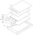
도 1은 제 1 실시예에 따른 액정표시장치를 도시한 분해 사시도이다.
도 2는 도 1에서 A-A`를 따라서 절단한 단면을 도시한 단면도이다.
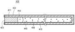
도 3은 제 1 실시예에 따른 파장 변환 부재를 도시한 사시도이다.
도 4는 도 3에서 B-B`를 따라서 절단한 단면을 도시한 단면도이다.
도 5는 파장 변환 부재의 다른 형태를 도시한 단면도이다.
도 6 내지 도 11은 실시예에 따른 파장 변환 부재를 제조하는 과정을 도시한 도면들이다.
도 12는 제 2 실시예에 따른 파장 변환 부재를 도시한 단면도이다.
도 13 내지 도 15는 제 2 실시예에 따른 파장 변환 부재를 제조하는 과정을 도시한 도면들이다.1 is an exploded perspective view of a liquid crystal display according to a first embodiment.
FIG. 2 is a cross-sectional view showing a section cut along AA 'in FIG. 1; FIG.
3 is a perspective view showing the wavelength conversion member according to the first embodiment.
FIG. 4 is a cross-sectional view showing a section cut along BB 'in FIG. 3; FIG.
5 is a cross-sectional view showing another form of the wavelength conversion member.
6 to 11 are views illustrating a process of manufacturing the wavelength conversion member according to the embodiment.
12 is a sectional view showing the wavelength conversion member according to the second embodiment.
13 to 15 are views illustrating a process of manufacturing the wavelength conversion member according to the second embodiment.
실시 예의 설명에 있어서, 각 기판, 프레임, 시트, 층 또는 패턴 등이 각 기판, 프레임, 시트, 층 또는 패턴 등의 "상(on)"에 또는 "아래(under)"에 형성되는 것으로 기재되는 경우에 있어, "상(on)"과 "아래(under)"는 "직접(directly)" 또는 "다른 구성요소를 개재하여 (indirectly)" 형성되는 것을 모두 포함한다. 또한 각 구성요소의 상 또는 아래에 대한 기준은 도면을 기준으로 설명한다. 도면에서의 각 구성요소들의 크기는 설명을 위하여 과장될 수 있으며, 실제로 적용되는 크기를 의미하는 것은 아니다.In the description of the embodiments, it is described that each substrate, frame, sheet, layer or pattern, etc., is formed on or "under" of each substrate, frame, sheet, layer or pattern, etc. In the case, “on” and “under” include both being formed “directly” or “indirectly” through other components. In addition, the upper or lower reference of each component is described with reference to the drawings. The size of each component in the drawings may be exaggerated for the sake of explanation and does not mean the size actually applied.
도 1은 제 1 실시예에 따른 액정표시장치를 도시한 분해 사시도이다. 도 2는 도 1에서 A-A`를 따라서 절단한 단면을 도시한 단면도이다. 도 3은 제 1 실시예에 따른 파장 변환 부재를 도시한 사시도이다. 도 4는 도 3에서 B-B`를 따라서 절단한 단면을 도시한 단면도이다. 도 5는 파장 변환 부재의 다른 형태를 도시한 단면도이다. 도 6 내지 도 11은 실시예에 따른 파장 변환 부재를 제조하는 과정을 도시한 도면들이다.1 is an exploded perspective view showing a liquid crystal display device according to a first embodiment. FIG. 2 is a cross-sectional view illustrating a cross section taken along line AA ′ in FIG. 1. 3 is a perspective view showing the wavelength conversion member according to the first embodiment. Fig. 4 is a cross-sectional view showing a section cut along the line B-B 'in Fig. 3; Fig. 5 is a cross-sectional view showing another form of the wavelength conversion member. 6 to 11 are views illustrating a process of manufacturing the wavelength conversion member according to the embodiment.
도 1 내지 도 4를 참조하면, 실시예에 따른 액정표시장치는 몰드 프레임(10), 백라이트 어셈블리(20) 및 액정패널(30)을 포함한다.1 to 4, a liquid crystal display device according to an embodiment includes a
상기 몰드 프레임(10)은 상기 백라이트 어셈블리(20) 및 상기 액정패널(30)을 수용한다. 상기 몰드 프레임(10)은 사각 틀 형상을 가지며, 상기 몰드 프레임(10)으로 사용하는 물질의 예로서는 플라스틱 또는 강화 플라스틱 등을 들 수 있다.The
또한, 상기 몰드 프레임(10) 아래에는 상기 몰드 프레임(10)을 감싸며, 상기 백라이트 어셈블리(20)를 지지하는 샤시가 배치될 수 있다. 상기 샤시는 상기 몰드 프레임(10)의 측면에도 배치될 수 있다.In addition, a chassis supporting the
상기 백라이트 어셈블리(20)는 상기 몰드 프레임(10) 내측에 배치되며, 광을 발생시켜 상기 액정패널(30)을 향하여 출사한다. 상기 백라이트 어셈블리(20)는 반사시트(100), 도광판(200), 발광다이오드(300), 파장 변환 부재(400), 다수 개의 광학 시트들(500) 및 연성인쇄회로기판(flexible printed circuit board;FPCB)(600)을 포함한다.The
상기 반사시트(100)는 상기 발광다이오드(300)로부터 발생하는 광을 상방으로 반사시킨다.The
상기 도광판(200)은 상기 반사시트(100) 상에 배치되며, 상기 발광다이오드(300)로부터 출사되는 광을 입사받아, 반사, 굴절 및 산란 등을 통해서 상방으로 가이드한다.The
상기 도광판(200)은 상기 발광다이오드(300)를 향하는 입사면을 포함한다. 즉, 상기 도광판(200)의 측면들 중 상기 발광다이오드(300)를 향하는 면이 입사면이다.The
상기 발광다이오드(300)는 상기 도광판(200)의 측면에 배치된다. 더 자세하게, 상기 발광다이오드(300)는 상기 입사면에 배치된다.The
상기 발광다이오드(300)는 광을 발생시키는 광원이다. 더 자세하게, 상기 상기 발광다이오드(300)는 상기 파장 변환 부재(400)를 향하여 광을 출사한다.The
상기 발광다이오드(300)는 청색 광을 발생시키는 청색 발광다이오드 또는 자외선을 발생시키는 UV 발광다이오드일 수 있다. 즉, 상기 발광다이오드(300)는 약 430㎚ 내지 약 470㎚ 사이의 파장대를 가지는 청색광 또는 약 300㎚ 내지 약 400㎚ 사이의 파장대를 가지는 자외선을 발생시킬 수 있다.The
상기 발광다이오드(300)는 상기 연성인쇄회로기판(600)에 실장된다. 상기 발광다이오드(300)는 상기 연성인쇄회로기판(600) 아래에 배치된다. 상기 발광다이오드(300)는 상기 연성인쇄회로기판(600)을 통하여 구동신호를 인가받아 구동된다.The
상기 파장 변환 부재(400)는 상기 발광다이오드(300) 및 상기 도광판(200) 사이에 개재된다. 상기 파장 변환 부재(400)는 상기 도광판(200)의 측면에 접착된다. 더 자세하게, 상기 파장 변환 부재(400)는 상기 도광판(200)의 입사면에 부착된다. 또한, 상기 파장 변환 부재(400)는 상기 발광다이오드(300)에 접착될 수 있다.The
상기 파장 변환 부재(400)는 상기 발광다이오드(300)로부터 출사되는 광을 입사받아, 파장을 변환시킨다. 예를 들어, 상기 파장 변환 부재(400)는 상기 발광다이오드(300)로부터 출사되는 청색광을 녹색광 및 적색광으로 변환시킬 수 있다. 즉, 상기 파장 변환 부재(400)는 상기 청색광의 일부를 약 520㎚ 내지 약 560㎚ 사이의 파장대를 가지는 녹색광으로 변환시키고, 상기 청색광의 다른 일부를 약 630㎚ 내지 약 660㎚ 사이의 파장대를 가지는 적색광으로 변환시킬 수 있다.The
또한, 상기 파장 변환 부재(400)는 상기 발광다이오드(300)로부터 출사되는 자외선을 청색광, 녹색광 및 적색광으로 변환시킬 수 있다. 즉, 상기 파장 변환 부재(400)는 상기 자외선의 일부를 약 430㎚ 내지 약 470㎚ 사이의 파장대를 가지는 청색광으로 변환시키고, 상기 자외선의 다른 일부를 약 520㎚ 내지 약 560㎚ 사이의 파장대를 가지는 녹색광으로 변환시키고, 상기 자외선의 또 다른 일부를 약 630㎚ 내지 약 660㎚ 사이의 파장대를 가지는 적색광으로 변환시킬 수 있다.In addition, the
이에 따라서, 상기 파장 변환 부재(400)를 통과하는 광 및 상기 파장 변환 부재(400)에 의해서 변환된 광들은 백색광을 형성할 수 있다. 즉, 청색광, 녹색광 및 적색광이 조합되어, 상기 도광판(200)에는 백색광이 입사될 수 있다.Accordingly, the light passing through the
도 3 및 도 4에 도시된 바와 같이, 상기 파장 변환 부재(400)는 튜브(410), 전처리층(421), 밀봉부(420), 다수 개의 파장 변환 입자들(430) 및 호스트(440)를 포함한다.As shown in FIGS. 3 and 4, the
상기 튜브(410)는 상기 파장 변환 입자들(430) 및 상기 호스트(440)를 수용한다. 즉, 상기 튜브(410)는 상기 파장 변환 입자들(430) 및 상기 호스트(440)를 수용하는 수용부이다. 또한, 상기 튜브(410)는 일 방향으로 길게 연장되는 형상을 가진다.The
상기 튜브(410)의 양 끝단은 밀봉된다. 상기 튜브(410)의 일 끝단은 상기 밀봉부(420)에 의해서 밀봉된다. 상기 튜브(410)는 상기 파장 변환 입자들(430) 및 상기 호스트(440)를 둘러싼다. 상기 튜브(410)는 상기 파장 변환 입자들(430) 및 상기 호스트(440)를 수용한다. 즉, 상기 튜브(410)는 내부에 빈 공간을 형성하고, 상기 빈 공간에 상기 파장 변환 입자들(430) 및 상기 호스트(440)를 수용한다. 상기 튜브(410)는 상기 파장 변환 입자들(430)을 수용하는 수용부이다.Both ends of the
상기 튜브(410)는 일 방향으로 연장되는 형상을 가진다. 상기 튜브(410)는 파이프 형상을 가진다. 상기 튜브(410)는 사각 파이프 형상을 가질 수 있다. 즉, 상기 튜브(410)의 길이 방향에 대하여 수직한 단면은 직사각형 형상을 가질 수 있다. 또한, 상기 튜브(410)의 폭은 약 0.6㎜이고, 상기 튜브(410)의 높이는 약 0.2㎜일 수 있다. 즉, 상기 튜브(410)는 모세관일 수 있다.The
상기 튜브(410)는 투명하다. 상기 튜브(410)로 사용되는 물질의 예로서는 유리 등을 들 수 있다. 즉, 상기 튜브(410)는 유리 모세관일 수 있다.The
상기 전처리층(421)은 상기 튜브(410)의 적어도 일면에 배치될 수 있다. 더 자세하게, 상기 전처리층(421)은 상기 튜브(410)의 일부 표면 또는 전체 표면에 배치될 수 있다. 또한, 상기 전처리층(421)은 상기 튜브(410)의 내부면에 배치될 수 있다.The
또한, 상기 전처리층(421)은 상기 밀봉부(420) 및 상기 튜브(410)의 내부면 사이에 개재될 수 있다. 상기 전처리층(421)은 상기 튜브(410)의 입구(411) 부분에 배치될 수 있다. 또한, 상기 전처리층(421)은 상기 튜브(410)의 외부면에도 형성될 수 있다. 즉, 상기 전처리층(421)은 상기 튜브(410)의 입구(411)의 내부면 및 외부면에 코팅될 수 있다. 또한, 상기 전처리층(421)은 상기 밀봉부(420) 및 상기 튜브(410)에 직접 접촉될 수 있다.In addition, the
또한, 도 5에 도시된 바와 같이, 상기 전처리층(422)은 상기 튜브(410)의 내부면 및 외부면에 전체적으로 형성될 수 있다. 이에 따라서, 상기 전처리층(422)은 상기 튜브(410)의 내부면 및 상기 호스트(440) 사이에도 개재될 수 있다.In addition, as shown in FIG. 5, the
상기 전처리층(421)은 상기 밀봉부(420) 및 상기 튜브(410)에 향상된 접착력을 가질 수 있다. 이에 따라서, 상기 전처리층(421)은 상기 밀봉부(420) 및 상기 튜브(410) 사이의 접착력 및 밀봉력을 향상시킬 수 있다. 즉, 상기 전처리층(421)은 상기 밀봉부(420) 및 상기 튜브(410) 사이에서 버퍼 기능을 수행하는 버퍼층일 수 있다.The
상기 전처리층(421)은 및 상기 튜브(410)에 화학적으로 결합될 수 있다. 또한, 상기 전처리층(421)은 상기 밀봉부(420)와 동일한 표면 특성을 가질 수 있다. 예를 들어, 상기 전처리층(421) 및 상기 밀봉부(420)가 모두 친수성을 가지거나, 모두 소수성을 가질 수 있다. 이에 따라서, 상기 밀봉부(420)는 상기 전처리층(421)을 통하여 상기 튜브(410)를 효과적으로 밀봉할 수 있다.The
상기 전처리층(421)으로 유기 물질이 사용될 수 있다. 상기 전처리층(421)으로 사용되는 물질의 예로서는 치환 또는 치환되지 않는 실란이 사용될 수 있다. 더 자세하게, 상기 전처리층(421)으로 에폭시기 또는 아미노기 등으로 치환된 실란이 사용될 수 있다. 즉, 상기 전처리층(421)으로 에폭시 실란 또는 아미노 실란 등이 사용될 수 있다.An organic material may be used as the
상기 밀봉부(420)는 상기 튜브(410)의 일 끝단에 배치된다. 상기 밀봉부(420)는 상기 튜브(410)의 입부에 배치된다. 더 자세하게, 상기 밀봉부(420)는 상기 튜브(410)의 입구(411) 부분에 채워진다. 즉, 상기 밀봉부(420)는 상기 튜브(410)의 입구(411)를 밀봉할 수 있다. 상기 밀봉부(420)는 상기 파장 변환 입자들(430) 및 상기 호스트(440)를 상기 튜브(410)의 내부에서 밀봉할 수 있다.The
상기 밀봉부(420)는 상기 전처리층(421) 내에 배치된다. 상기 밀봉부(420)는 상기 전처리층(421)과 직접 접촉된다. 더 자세하게, 상기 밀봉부(420)는 상기 전처리층(421)과 화학적으로 결합될 수 있다.The
상기 밀봉부(420)로 유기 물질이 사용될 수 있다. 상기 밀봉부(420)로 페놀 수지, 요소 수지, 멜라민 수지, 아크릴계 수지, 에폭시계 수지 또는 실리콘계 수지 등이 사용될 수 있다.An organic material may be used as the
상기 파장 변환 입자들(430)은 상기 튜브(410)의 내부에 배치된다. 더 자세하게, 상기 파장 변환 입자들(430)은 상기 호스트(440)에 균일하게 분산되고, 상기 호스트(440)는 상기 튜브(410)의 내부에 배치된다.The
상기 파장 변환 입자들(430)은 상기 발광다이오드(300)로부터 출사되는 광의 파장을 변환시킨다. 상기 파장 변환 입자들(430)은 상기 발광다이오드(300)로부터 출사되는 광을 입사받아, 파장을 변환시킨다. 예를 들어, 상기 파장 변환 입자들(430)은 상기 발광다이오드(300)로부터 출사되는 청색광을 녹색광 및 적색광으로 변환시킬 수 있다. 즉, 상기 파장 변환 입자들(430) 중 일부는 상기 청색광을 약 520㎚ 내지 약 560㎚ 사이의 파장대를 가지는 녹색광으로 변환시키고, 상기 파장 변환 입자들(430) 중 다른 일부는 상기 청색광을 약 630㎚ 내지 약 660㎚ 사이의 파장대를 가지는 적색광으로 변환시킬 수 있다.The
이와는 다르게, 상기 파장 변환 입자들(430)은 상기 발광다이오드(300)로부터 출사되는 자외선을 청색광, 녹색광 및 적색광으로 변환시킬 수 있다. 즉, 상기 파장 변환 입자들(430) 중 일부는 상기 자외선을 약 430㎚ 내지 약 470㎚ 사이의 파장대를 가지는 청색광으로 변환시키고, 상기 파장 변환 입자들(430) 중 다른 일부는 상기 자외선을 약 520㎚ 내지 약 560㎚ 사이의 파장대를 가지는 녹색광으로 변환시킬 수 있다. 또한, 상기 파장 변환 입자들(430) 중 또 다른 일부는 상기 자외선을 약 630㎚ 내지 약 660㎚ 사이의 파장대를 가지는 적색광으로 변환시킬 수 있다.Alternatively, the
즉, 상기 발광다이오드(300)가 청색광을 발생시키는 청색 발광다이오드인 경우, 청색광을 녹색광 및 적색광으로 각각 변환시키는 파장 변환 입자들(430)이 사용될 수 있다. 이와는 다르게, 상기 발광다이오드(300)가 자외선을 발생시키는 UV 발광다이오드인 경우, 자외선을 청색광, 녹색광 및 적색광으로 각각 변환시키는 파장 변환 입자들(430)이 사용될 수 있다.That is, when the
상기 파장 변환 입자들(430)은 양자점(QD, Quantum Dot)일 수 있다. 상기 양자점은 코어 나노 결정 및 상기 코어 나노 결정을 둘러싸는 껍질 나노 결정을 포함할 수 있다. 또한, 상기 양자점은 상기 껍질 나노 결정에 결합되는 유기 리간드를 포함할 수 있다. 또한, 상기 양자점은 상기 껍질 나노 결정을 둘러싸는 유기 코팅층을 포함할 수 있다.The
상기 껍질 나노 결정은 두 층 이상으로 형성될 수 있다. 상기 껍질 나노 결정은 상기 코어 나노 결정의 표면에 형성된다. 상기 양자점은 상기 코어 나오 결정으로 입광되는 빛의 파장을 껍질층을 형성하는 상기 껍질 나노 결정을 통해서 파장을 길게 변환시키고 빛의 효율을 증가시길 수 있다.The shell nanocrystals may be formed of two or more layers. The shell nanocrystals are formed on the surface of the core nanocrystals. The quantum dot may convert the wavelength of the light incident on the core core crystal into a long wavelength through the shell nanocrystals forming the shell layer and increase the light efficiency.
상기 양자점은 Ⅱ족 화합물 반도체, Ⅲ족 화합물 반도체, Ⅴ족 화합물 반도체 그리고 VI족 화합물 반도체 중에서 적어도 한가지 물질을 포함할 수 있다. 보다 상세하게, 상기 코어 나노 결정은 Cdse, InGaP, CdTe, CdS, ZnSe, ZnTe, ZnS, HgTe 또는 HgS를 포함할 수 있다. 또한, 상기 껍질 나노 결정은 CuZnS, CdSe, CdTe, CdS, ZnSe, ZnTe, ZnS, HgTe 또는 HgS를 포함할 수 있다. 상기 양자점의 지름은 1 nm 내지 10 nm일 수 있다.The quantum dot may include at least one of a group II compound semiconductor, a group III compound semiconductor, a group V compound semiconductor, and a group VI compound semiconductor. More specifically, the core nanocrystals may include Cdse, InGaP, CdTe, CdS, ZnSe, ZnTe, ZnS, HgTe or HgS. The shell nanocrystals may include CuZnS, CdSe, CdTe, CdS, ZnSe, ZnTe, ZnS, HgTe or HgS. The diameter of the quantum dot may be 1 nm to 10 nm.
상기 양자점에서 방출되는 빛의 파장은 상기 양자점의 크기 또는 합성 과정에서의 분자 클러스터 화합물(molecular cluster compound)와 나노입자 전구체 (precurser)의 몰분율 (molar ratio)에 따라 조절이 가능하다. 상기 유기 리간드는 피리딘(pyridine), 메르캅토 알콜(mercapto alcohol), 티올(thiol), 포스핀(phosphine) 및 포스핀 산화물(phosphine oxide) 등을 포함할 수 있다. 상기 유기 리간드는 합성 후 불안정한 양자점을 안정화시키는 역할을 한다. 합성 후에 댕글링 본드(dangling bond)가 외곽에 형성되며, 상기 댕글링 본드 때문에, 상기 양자점이 불안정해 질 수도 있다. 그러나, 상기 유기 리간드의 한 쪽 끝은 비결합 상태이고, 상기 비결합된 유기 리간드의 한 쪽 끝이 댕글링 본드와 결합해서, 상기 양자점을 안정화 시킬 수 있다.The wavelength of light emitted from the quantum dots can be controlled by the size of the quantum dots or the molar ratio of the molecular cluster compound and the nanoparticle precursor in the synthesis process. The organic ligand may include pyridine, mercapto alcohol, thiol, phosphine, phosphine oxide, and the like. The organic ligands serve to stabilize unstable quantum dots after synthesis. After synthesis, a dangling bond is formed on the outer periphery, and the quantum dots may become unstable due to the dangling bonds. However, one end of the organic ligand is in an unbonded state, and one end of the unbound organic ligand bonds with the dangling bond, thereby stabilizing the quantum dot.
특히, 상기 양자점은 그 크기가 빛, 전기 등에 의해 여기되는 전자와 정공이 이루는 엑시톤(exciton)의 보어 반경(Bohr raidus)보다 작게 되면 양자구속효과가 발생하여 띄엄띄엄한 에너지 준위를 가지게 되며 에너지 갭의 크기가 변화하게 된다. 또한, 전하가 양자점 내에 국한되어 높은 발광효율을 가지게 된다.Particularly, when the quantum dot has a size smaller than the Bohr radius of an exciton formed by electrons and holes excited by light, electricity or the like, a quantum confinement effect is generated to have a staggering energy level and an energy gap The size of the image is changed. Further, the charge is confined within the quantum dots, so that it has a high luminous efficiency.
이러한 상기 양자점은 일반적 형광 염료와 달리 입자의 크기에 따라 형광파장이 달라진다. 즉, 입자의 크기가 작아질수록 짧은 파장의 빛을 내며, 입자의 크기를 조절하여 원하는 파장의 가시광선영역의 형광을 낼 수 있다. 또한, 일반적 염료에 비해 흡광계수(extinction coefficient)가 100~1000배 크고 양자효율(quantum yield)도 높으므로 매우 센 형광을 발생한다.Unlike general fluorescent dyes, the quantum dots vary in fluorescence wavelength depending on the particle size. That is, as the size of the particle becomes smaller, it emits light having a shorter wavelength, and the particle size can be adjusted to produce fluorescence in a visible light region of a desired wavelength. In addition, since the extinction coefficient is 100 to 1000 times higher than that of a general dye, and the quantum yield is also high, it produces very high fluorescence.
상기 양자점은 화학적 습식방법에 의해 합성될 수 있다. 여기에서, 화학적 습식방법은 유기용매에 전구체 물질을 넣어 입자를 성장시키는 방법으로서, 화학적 습식방법에 의해서, 상기 양자점이 합성될 수 있다.The quantum dot can be synthesized by a chemical wet process. Here, the chemical wet method is a method of growing particles by adding a precursor material to an organic solvent, and the quantum dots can be synthesized by a chemical wet method.
상기 호스트(440)는 상기 파장 변환 입자들(430)을 둘러싼다. 즉, 상기 호스트(440)는 상기 파장 변환 입자들(430)을 균일하게 내부에 분산시킨다. 상기 호스트(440)는 폴리머로 구성될 수 있다. 상기 호스트(440)는 투명하다. 즉, 상기 호스트(440)는 투명한 폴리머로 형성될 수 있다.The
상기 호스트(440)는 상기 튜브(410) 내부에 배치된다. 즉, 상기 호스트(440)는 전체적으로 상기 튜브(410) 내부에 채워진다. 상기 호스트(440)는 상기 튜브(410)의 내면에 밀착될 수 있다.The
상기 호스트(440)로 광 경화성 수지가 사용될 수 있다. 상기 호스트(440)로 실리콘계 수지, 에폭시계 수지 또는 아크릴계 수지 등이 사용될 수 있다.Photocurable resin may be used as the
상기 밀봉부(420) 및 상기 호스트(440) 사이에는 공기층(450)이 형성된다. 상기 공기층(450)에는 질소로 채워진다. 상기 공기층(450)은 상기 밀봉부(420) 및 상기 호스트(440) 사이에서 완충 기능을 수행한다.An
상기 호스트(440)는 상기 전처리층(421)과 다른 표면 특성을 가질 수 있다. 더 자세하게, 상기 호스트(440)는 제 1 표면 특성을 가지고, 상기 전처리층(421)은 제 2 표면 특성을 가질 수 있다. 또한, 상기 튜브(410)의 내부면은 상기 호스트(440)와 같은 표면 특성을 가질 수 있다. 또한, 상기 밀봉부(420)는 상기 전처리층(421)과 같은 표면 특성을 가질 수 있다.The
예들 들어, 상기 호스트(440) 및 상기 튜브(410)의 내부면은 소수성을 가지고, 상기 전처리층(421) 및 상기 밀봉부(420)는 친수성을 가질 수 있다. 이와는 반대로, 상기 호스트(440) 및 상기 튜브(410)의 내부면은 친수성을 가지고, 상기 전처리층(421) 및 상기 밀봉부(420)는 소수성을 가질 수 있다.For example, the inner surfaces of the
더 자세하게, 상기 호스트(440)는 상기 파장 변환 입자들(430)의 특성에 따라서, 사용되는 수지가 정해질 수 있다. 즉, 상기 호스트(440)으로 사용되는 수지는 상기 파장 변환 입자들(430)의 특성을 극대화 시키기 위해서 선택될 수 있다. 결과적으로, 상기 호스트(440)는 상기 파장 변환 입자들(430)에 따라서, 더 자세하게, 상기 코어 나노 결정, 껍질 나노 결정 및 상기 리간드의 종류에 따라서, 상기 호스트(440)으로 사용되는 수지가 정해질 수 있다. 이에 따라서, 상기 호스트(440)는 친수성을 가지거나, 소수성을 가질 수 있다.In more detail, the
상기 호스트(440)가 친수성을 가지는 경우, 상기 전처리층(421)은 소수성을 가질 수 있다. 이에 따라서, 상기 전처리층(421)으로 사용되는 수지는 소수성기를 포함할 수 있다. 또한, 상기 밀봉부(420)도 소수성을 가질 수 있다. 이에 따라서, 상기 밀봉부(420)로 사용되는 수지는 소수성기를 포함할 수 있다.When the
상기 호스트(440)가 소수성을 가지는 경우, 상기 전처리층(421)은 친수성을 가질 수 있다. 이에 따라서, 상기 전처리층(421)으로 사용되는 수지는 친수성기를 포함할 수 있다. 또한, 상기 밀봉부(420)도 친수성을 가질 수 있다. 이에 따라서, 상기 밀봉부(420)로 사용되는 수지는 친수성기를 포함할 수 있다.When the
상기 친수성기는 물분자와 친화력을 가진다. 상기 친수성기의 예로서는 -OH, NH2, -COOH, -OSO3H 또는 -OPO3H2 등을 들 수 있다. 상기 소수성기는 물과 반발성을 가지는 관능기이다. 상기 소수성기의 예로서는 사슬모양 탄화수소기, 방향족탄화수소기, 할로젠화알킬기 도는 유기규소기 등을 들 수 있다.The hydrophilic group has affinity with water molecules. Examples of the hydrophilic group include -OH, NH2 , -COOH, -OSO3 H or -OPO3 H2 . The hydrophobic group is a functional group having water and repulsion. Examples of the hydrophobic group include a chain hydrocarbon group, an aromatic hydrocarbon group, a halogenated alkyl group or an organosilicon group.
상기 파장 변환 부재(400)는 다음과 같은 방법에 의해서 형성될 수 있다.The
도 6을 참조하면, 튜브(410)의 입구에 전처리층(421)을 형성하기 위해서, 제 1 수지 조성물(423)이 코팅된다. 상기 제 1 수지 조성물(423)은 치환 또는 치환되지 않는 실란을 포함할 수 있다. 더 자세하게, 상기 제 1 수지 조성물(423)은 치환 또는 치환되지 않는 에폭시 실란 또는 치환 또는 치환되지 않는 아미노 실란을 포함할 수 있다.Referring to FIG. 6, the
상기 제 1 수지 조성물(423)은 추후에 호스트(440)를 형성하기 위한 제 2 수지 조성물(440a)의 특성에 따라서 친수성 또는 소수성을 가질 수 있다. 즉, 상기 제 2 수지 조성물(440a)이 친수성을 가지는 경우, 상기 제 1 수지 조성물(423)은 소수성기를 가진다. 이와는 반대로, 상기 제 2 수지 조성물(440a)이 소수성을 가지는 경우, 상기 제 1 수지 조성물(423)은 친수성기를 가질 수 있다.The
도 7을 참조하면, 상기 튜브(410)의 입구에 코팅된 제 1 수지 조성물(423)은 자외선 및/또는 열에 의해서 경화된다. 이에 따라서, 상기 튜브(410)의 입구의 내부면 및 외부면에 상기 전처리층(421)이 형성된다.Referring to FIG. 7, the
위와는 다르게, 도 8을 참조하면, 상기 전처리층(421)은 상기 튜브(410)의 내부면 및 외부면 전체에 형성될 수 있다. 상기 전처리층(421)은 증발법 또는 화학 기상 증착 공정 등과 같은 진공 증착 공정에 의해서 형성될 수 있다. 더 자세하게, 치환 또는 치환되지 않는 에폭시 실란(epoxy silane) 또는 치환 또는 치환되지 않는 아미노 실란(amino silane) 등이 증발되어, 상기 튜브(410)에 상기 전처리층(421)이 형성될 수 있다.Unlike the above, referring to FIG. 8, the
도 9를 참조하면, 제 2 수지 조성물(440a)에 상기 파장 변환 입자들(430)이 균일하게 분산된다. 상기 제 2 수지 조성물(440a)은 투명하다. 상기 제 2 수지 조성물(440a)은 광 경화성을 가질 수 있다.9, the
이후, 상기 튜브(410)의 내부는 감압되고, 상기 파장 변환 입자들(430)이 분산된 제 2 수지 조성물(440a)에 상기 튜브(410)의 입구(411)가 딥핑되고, 주위의 압력이 상승된다. 이에 따라서, 상기 파장 변환 입자들(430)이 분산된 제 2 수지 조성물(440a)은 상기 튜브(410) 내부로 유입된다.Thereafter, the inside of the
도 10을 참조하면, 상기 튜브(410) 내로 유입된 제 2 수지 조성물(440a)의 일부가 제거되고, 상기 튜브(410)의 입구(411) 부분이 비워진다.Referring to FIG. 10, a portion of the
이때, 상기 제 2 수지 조성물(440a)은 상기 전처리층(421)과 다른 표면 특성을 가지기 때문에, 상기 튜브(410)의 입부 부분에는 상기 제 2 수지 조성물(440a)이 잔유하지 않게 된다. 즉, 상기 제 2 수지 조성물(440a)이 친수성을 가지는 경우, 상기 전처리층(421)은 소수성을 가지도록 형성되고, 상기 제 2 수지 조성물(440a)이 소수성을 가지는 경우, 상기 전처리층(421)은 친수성을 가지도록 형성된다.In this case, since the
이에 따라서, 상기 튜브(410)의 입구 부분의 제 2 수지 조성물(440a)은 용이하고, 깨끗하게 제거될 수 있다. 따라서, 상기 튜브(410)의 입구 부분의 전처리층(421) 상에는 상기 제 2 수지 조성물(440a)이 잔유하지 않는다.Accordingly, the
이후, 상기 튜브(410) 내로 유입된 수지 조성물(440a)은 자외선 등에 의해서 경화되고, 상기 호스트(440)가 형성된다.Thereafter, the
도 11을 참조하면, 상기 튜브(410)의 입구(411)에 밀봉부(420)가 형성된다. 상기 밀봉부(420)를 형성하기 위해서, 상기 튜브(410)의 입구에 제 3 수지 조성물이 유입된다. 상기 제 3 수지 조성물은 상기 전처리층(421)과 동일한 특성을 가질 수 있다. 즉, 상기 전처리층(421)이 친수성을 가지는 경우, 상기 제 3 수지 조성물은 친수성을 가질 수 있다. 또한, 상기 전처리층(421)이 소수성을 가지는 경우, 상기 제 3 수지 조성물은 소수성을 가질 수 있다.Referring to FIG. 11, a
이후, 상기 튜브(410)의 입구에 유입된 제 3 수지 조성물은 자외선 및/또는 열에 의해서 경화되고, 상기 밀봉부(420)가 형성된다.Thereafter, the third resin composition introduced into the inlet of the
상기 밀봉부(420)가 형성되는 공정은 질소 분위기에서 진행되고, 이에 따라서, 질소를 포함하는 공기층(450)이 상기 밀봉부(420) 및 상기 호스트(440) 사이에 형성될 수 있다.The process of forming the
다시 도 1 및 도 2를 참조하면, 상기 광학 시트들(500)은 상기 도광판(200) 상에 배치된다. 상기 광학 시트들(500)은 통과하는 광의 특성을 향상시킨다.Referring back to FIGS. 1 and 2, the
상기 연성인쇄회로기판(600)은 상기 발광다이오드(300)에 전기적으로 연결된다. 상기 발광다이오드(300)를 실장할 수 있다. 상기 연성인쇄회로기판(600)은 연성인쇄회로기판이며, 상기 몰드 프레임(10) 내측에 배치된다. 상기 연성인쇄회로기판(600)은 상기 도광판(200) 상에 배치된다.The flexible printed
상기 몰드 프레임(10) 및 상기 백라이트 어셈블리(20)에 의해서, 백라이트 유닛이 구성된다. 즉, 상기 백라이트 유닛은 상기 몰드 프레임(10) 및 상기 백라이트 어셈블리(20)를 포함한다.The backlight unit is configured by the
상기 액정패널(30)은 상기 몰드 프레임(10) 내측에 배치되고, 상기 광학시트들(500)상에 배치된다.The
상기 액정패널(30)은 통과하는 광의 세기를 조절하여 영상을 표시한다. 즉, 상기 액정패널(300)은 영상을 표시하는 표시패널이다. 더 자세하게, 상기 액정패널은 상기 파장 변환 부재(400)에 의해서 파장이 변환된 광을 이용하여 영상을 표시한다.The
상기 액정패널(30)은 TFT기판, 컬러필터기판, 두 기판들 사이에 개재되는 액정층 및 편광필터들을 포함한다.The
앞서 설명한 바와 같이, 상기 전처리층(421)은 상기 호스트(440)과 다른 표면 특성을 가지기 때문에, 상기 호스트(440)를 형성하는 과정에서 상기 튜브(410)의 입구에는 상기 제 2 수지 조성물(440a)이 잔유하지 않게 된다.As described above, since the
이에 따라서, 상기 밀봉부(420)는 상기 전처리층(421)에 견고하게 접합될 수 있다. 특히, 상기 밀봉부(420)는 상기 전처리층(421)과 동일한 표면 특성을 가지기 때문에, 상기 밀봉부(420) 및 상기 전처리층(421)은 서로 견고하게 결합될 수 있다.Accordingly, the sealing
또한, 상기 전처리층(421)은 상기 튜브(410)의 입구의 내부면 및 외부면에 코팅된다. 이에 따라서, 전처리층(421) 및 상기 튜브(410)의 입구는 넓은 면적으로 서로 접촉될 수 있다.In addition, the
결국, 상기 밀봉부(420) 및 상기 전처리층(421)은 상기 튜브(410)의 내부를 견고하게 밀봉할 수 있다.As a result, the
따라서, 상기 파장 변환 입자들(430)은 외부의 습기 및 산소 등에 의해서 손상되지 않는다. 따라서, 상기 파장 변환 부재(400)는 외부의 화학적인 충격으로부터 파장 변환 입자들(430)을 효과적으로 보호할 수 있다.Therefore, the
따라서, 실시예에 따른 액정표시장치는 향상된 신뢰성 및 내 화학성을 가질 수 있다.
Therefore, the liquid crystal display according to the embodiment may have improved reliability and chemical resistance.
도 12는 제 2 실시예에 따른 파장 변환 부재를 도시한 단면도이다. 도 13 내지 도 15는 제 2 실시예에 따른 파장 변환 부재를 제조하는 과정을 도시한 도면들이다. 본 실시예에서는 튜브에 대해서 추가로 설명하고, 앞선 실시예에 대한 설명을 참고한다. 즉, 앞선 실시예에 대한 설명은 변경된 부분을 제외하고, 본 실시예에 대한 설명에 본질적으로 결합될 수 있다.12 is a sectional view showing the wavelength conversion member according to the second embodiment. 13 to 15 are views illustrating a process of manufacturing the wavelength conversion member according to the second embodiment. In this embodiment, the tube is further described, and reference is made to the description of the foregoing embodiment. That is, the description of the foregoing embodiment may be essentially combined with the description of the present embodiment except for the changed part.
도 12를 참조하면, 튜브(410)는 제 1 영역(R1) 및 제 2 영역(R2)을 포함한다. 상기 제 1 영역(R1)은 상기 튜브(410)의 입구 부분일 수 있다. 또한, 상기 제 2 영역(R2)은 상기 튜브(410)의 안쪽 부분일 수 있다. 더 자세하게, 상기 제 1 영역(R1)은 상기 튜브(410)의 일 끝단일 수 있다. 상기 제 2 영역(R2)은 상기 제 1 영역(R1)에 인접한 부분으로부터 상기 튜브(410)의 다른 끝단까지 일 수 있다. 즉, 상기 제 2 영역(R2)은 상기 튜브(410)의 입구 부분을 제외한 나머지 부분일 수 있다.Referring to FIG. 12, the
상기 제 1 영역(R1) 및 상기 제 2 영역(R2)은 서로 다른 표면 특성을 가질 수 있다. 즉, 상기 제 1 영역(R1)은 제 1 표면 특성을 가지고, 상기 제 2 영역(R2)은 제 2 표면 특성을 가질 수 있다. 더 자세하게, 상기 제 1 영역(R1)의 내부면은 제 1 표면 특성을 가지고, 상기 제 2 영역(R2)의 내부면은 제 2 표면 특성을 가질 수 있다. 더 자세하게, 상기 제 1 영역(R1)이 소수성을 가지는 경우, 상기 제 2 영역(R2)은 친수성을 가질 수 있다. 또한, 상기 제 1 영역(R1)이 친수성을 가지는 경우, 상기 제 2 영역(R2)은 소수성을 가질 수 있다.The first region R1 and the second region R2 may have different surface properties. That is, the first region R1 may have a first surface characteristic, and the second region R2 may have a second surface characteristic. In more detail, an inner surface of the first region R1 may have a first surface characteristic, and an inner surface of the second region R2 may have a second surface characteristic. In more detail, when the first region R1 has hydrophobicity, the second region R2 may have hydrophilicity. In addition, when the first region R1 has hydrophilicity, the second region R2 may have hydrophobicity.
상기 호스트(440)는 상기 제 2 영역(R2)에 배치된다. 상기 호스트(440)는 상기 제 2 영역(R2)에 직접 접촉될 수 있다. 상기 호스트(440)는 상기 제 2 영역(R2) 내에만 배치될 수 있다.The
또한, 상기 호스트(440)는 상기 제 2 영역(R2)과 같은 표면 특성을 가질 수 있다. 즉, 상기 호스트(440)는 제 2 표면 특성을 가질 수 있다. 이에 따라서, 상기 제 1 영역(R1)은 상기 호스트(440)와 다른 표면 특성을 가지게 된다. 즉, 상기 호스트(440)가 친수성을 가지는 경우, 상기 제 1 영역(R1)은 소수성을 가질 수 있다. 또한, 상기 호스트(440)가 소수성을 가지는 경우, 상기 제 1 영역(R1)은 친수성을 가질 수 있다.In addition, the
상기 밀봉부(420)는 상기 튜브(410)와 직접 접촉될 수 있다. 더 자세하게, 상기 제 1 영역(R1) 내에 배치된다. 상기 밀봉부(420)는 상기 제 1 영역(R1)의 내부면과 직접 접촉될 수 있다.The
상기 밀봉부(420)는 상기 제 1 영역(R1)과 동일한 표면 특성을 가질 수 있다. 즉, 상기 밀봉부(420)는 상기 제 1 표면 특성을 가질 수 있다. 즉, 상기 제 1 영역(R1)이 소수성을 가지는 경우, 상기 밀봉부(420)도 소수성을 가질 수 있다. 또한, 상기 제 1 영역(R1)이 친수성을 가지는 경우, 상기 밀봉부(420)도 친수성을 가질 수 있다.The sealing
본 실시예에 따른 파장 변환 부재(400)는 다음과 같은 과정에 의해서 형성될 수 있다.The
도 13을 참조하면, 튜브(410)의 입구 부분은 표면 처리 용액에 담겨지고, 표면 처리될 수 있다. 이에 따라서, 상기 튜브(410)의 입구 부분의 내부면 및 외부면은 개질되고, 상기 튜브(410)의 다른 부분과 다른 표면 특성을 가지게 된다. 즉, 상기 튜브(410)의 입구 부분은 친수성 또는 소수성을 가지도록 개질될 수 있다.Referring to FIG. 13, the inlet portion of the
예를 들어, 상기 튜브(410)가 유리를 포함하는 경우, 더 자세하게, 상기 튜브(410)가 유리로 형성되는 경우, 상기 표면 처리 용액은 헥사메틸 디실라잔(hexa methyl di silazane;HMDS) 또는 불화 암모늄을 포함할 수 있다. 이에 따라서, 상기 튜브(410)의 입구는 소수성을 가질 수 있다.For example, when the
도 14를 참조하면, 상기 튜브(410)는 세정되고, 상기 튜브(410) 내에 제 2 수지 조성물(440a)이 주입된다. 이후, 상기 튜브(410)의 입구 부분의 제 2 수지 조성물(440a)이 제거된다. 이때, 상기 제 1 영역(R1)은 상기 제 2 수지 조성물(440a)과 다른 표면 특성을 가지도록 개질되므로, 상기 제 1 영역(R1)에는 상기 제 2 수지 조성물(440a)이 남아있지 않게 된다.Referring to FIG. 14, the
이후, 상기 제 2 수지 조성물(440a)은 경화되고, 상기 튜브(410) 내에 호스트(440)가 형성된다.Thereafter, the
도 15를 참조하면, 상기 튜브(410)의 입구에 밀봉부(420)가 형성된다. 상기 밀봉부(420)가 형성되기 위해서, 상기 튜브(410)의 입구에 제 3 수지 조성물이 주입된다. 이후, 상기 제 3 수지 조성물은 경화되고, 상기 밀봉부(420)가 형성된다. 상기 밀봉부(420)는 상기 제 1 영역(R1)과 동일한 표면 특성을 가지기 때문에, 상기 튜브(410)의 내부면에 견고하게 결합될 수 있다.Referring to FIG. 15, a
앞서 설명한 바와 같이, 상기 제 1 영역(R1)은 상기 호스트(440)와 다른 표면 특성을 가지기 때문에, 상기 밀봉부(420) 및 상기 튜브(410) 사이에 잔유물이 개재되지 않는다. 또한, 상기 밀봉부(420) 및 상기 제 1 영역(R1)은 서로 강하게 결합되기 때문에, 상기 밀봉부(420) 및 상기 튜브(410)는 향상된 밀봉 특성을 가진다. 이에 따라서, 실시예에 따른 파장 변환 부재(400)는 향상된 신뢰성 및 내구성을 가질 수 있다.As described above, since the first region R1 has a surface property different from that of the
또한, 이상에서 실시예들에 설명된 특징, 구조, 효과 등은 본 발명의 적어도 하나의 실시예에 포함되며, 반드시 하나의 실시예에만 한정되는 것은 아니다. 나아가, 각 실시예에서 예시된 특징, 구조, 효과 등은 실시예들이 속하는 분야의 통상의 지식을 가지는 자에 의해 다른 실시예들에 대해서도 조합 또는 변형되어 실시 가능하다. 따라서 이러한 조합과 변형에 관계된 내용들은 본 발명의 범위에 포함되는 것으로 해석되어야 할 것이다.In addition, the features, structures, effects and the like described in the embodiments are included in at least one embodiment of the present invention, and are not necessarily limited to only one embodiment. Furthermore, the features, structures, effects, and the like illustrated in each embodiment may be combined or modified with respect to other embodiments by those skilled in the art to which the embodiments belong. Therefore, it should be understood that the present invention is not limited to these combinations and modifications.
이상에서 실시예를 중심으로 설명하였으나 이는 단지 예시일 뿐 본 발명을 한정하는 것이 아니며, 본 발명이 속하는 분야의 통상의 지식을 가진 자라면 본 실시예의 본질적인 특성을 벗어나지 않는 범위에서 이상에 예시되지 않은 여러 가지의 변형과 응용이 가능함을 알 수 있을 것이다. 예를 들어, 실시예에 구체적으로 나타난 각 구성 요소는 변형하여 실시할 수 있는 것이다. 그리고 이러한 변형과 응용에 관계된 차이점들은 첨부된 청구 범위에서 규정하는 본 발명의 범위에 포함되는 것으로 해석되어야 할 것이다.While the present invention has been particularly shown and described with reference to exemplary embodiments thereof, it is to be understood that the invention is not limited to the disclosed exemplary embodiments, but, on the contrary, It will be understood that various modifications and applications are possible. For example, each component specifically shown in the embodiments can be modified and implemented. It is to be understood that all changes and modifications that come within the meaning and range of equivalency of the claims are therefore intended to be embraced therein.
Claims (12)
Translated fromKorean상기 수용부 내에 배치되는 호스트;
상기 호스트 내에 배치되는 다수 개의 파장 변환 입자들;
상기 수용부의 내부에 배치되는 밀봉부; 및
상기 밀봉부 및 상기 수용부의 내부면 사이에 개재되는 전처리층을 포함하고,
상기 전처리층은 에폭시 실란 또는 아미노 실란을 포함하는 광학 부재.Receiving unit including an empty space therein;
A host disposed in the accommodating portion;
A plurality of wavelength converting particles disposed in the host;
A sealing part disposed inside the receiving part; And
It includes a pretreatment layer interposed between the sealing portion and the inner surface of the receiving portion,
The pretreatment layer includes an epoxy silane or an amino silane.
상기 밀봉부는 상기 수용부의 일 끝단에 배치되는 광학 부재.The method of claim 1, wherein the receiving portion has a shape extending in one direction,
The sealing member is disposed at one end of the receiving portion.
상기 호스트 및 상기 수용부의 내부면은 제 2 표면 특성을 가지는 광학 부재.The method of claim 1, wherein the sealing portion and the pretreatment layer has a first surface property,
An inner surface of the host and the receiving portion has a second surface characteristic.
상기 수용부 내에 배치되는 호스트;
상기 호스트 내에 배치되는 다수 개의 파장 변환 입자들; 및
상기 수용부 내에 배치되는 밀봉부를 포함하고,
상기 수용부의 내부면은
상기 밀봉부에 대응하고, 제 1 표면 특성을 가지는 제 1 영역; 및
상기 호스트에 대응하고, 제 2 표면 특성을 가지는 제 2 영역을 포함하고,
상기 호스트는 상기 제 1 표면 특성을 가지고,
상기 밀봉부는 상기 제 2 표면 특성을 가지는 광학 부재.An accommodation portion in which an empty space is formed;
A host disposed in the accommodating portion;
A plurality of wavelength converting particles disposed in the host; And
A seal disposed in the accommodation portion,
The inner surface of the receiving portion
A first region corresponding to the seal and having a first surface characteristic; And
A second region corresponding to said host, said second region having a second surface characteristic,
The host has the first surface property,
The sealing member has the second surface property.
상기 광원으로부터 출사되는 광이 입사되는 파장 변환 부재; 및
상기 파장 변환 부재로부터 출사되는 광이 입사되는 표시패널을 포함하고,
상기 파장 변환 부재는
내부에 빈 공간을 포함하는 수용부;
상기 수용부 내에 배치되는 호스트;
상기 호스트 내에 배치되는 다수 개의 파장 변환 입자들;
상기 수용부의 내부에 배치되는 밀봉부; 및
상기 밀봉부 및 상기 수용부의 내부면 사이에 개재되는 전처리층을 포함하고,
상기 전처리층은 에폭시 실란 또는 아미노 실란을 포함하는 표시장치.Light source;
A wavelength conversion member into which light emitted from the light source is incident; And
A display panel to which light emitted from the wavelength conversion member is incident;
The wavelength conversion member
Receiving unit including an empty space therein;
A host disposed in the accommodating portion;
A plurality of wavelength converting particles disposed in the host;
A sealing part disposed inside the receiving part; And
It includes a pretreatment layer interposed between the sealing portion and the inner surface of the receiving portion,
The pretreatment layer includes an epoxy silane or an amino silane.
상기 광원으로부터 출사되는 광이 입사되는 파장 변환 부재; 및
상기 파장 변환 부재로부터 출사되는 광이 입사되는 표시패널을 포함하고,
상기 파장 변환 부재는
내부에 빈 공간이 형성되는 수용부;
상기 수용부 내에 배치되는 호스트;
상기 호스트 내에 배치되는 다수 개의 파장 변환 입자들; 및
상기 수용부 내에 배치되는 밀봉부를 포함하고,
상기 수용부의 내부면은
상기 밀봉부에 대응하고, 제 1 표면 특성을 가지는 제 1 영역; 및
상기 호스트에 대응하고, 제 2 표면 특성을 가지는 제 2 영역을 포함하고,
상기 호스트는 상기 제 1 표면 특성을 가지고,
상기 밀봉부는 상기 제 2 표면 특성을 가지는 표시장치.Light source;
A wavelength conversion member into which light emitted from the light source is incident; And
A display panel to which light emitted from the wavelength conversion member is incident;
The wavelength conversion member
An accommodation portion in which an empty space is formed;
A host disposed in the accommodating portion;
A plurality of wavelength converting particles disposed in the host; And
A seal disposed in the accommodation portion,
The inner surface of the receiving portion
A first region corresponding to the seal and having a first surface characteristic; And
A second region corresponding to said host, said second region having a second surface characteristic,
The host has the first surface property,
And the sealing part has the second surface characteristic.
상기 수용부 내에 호스트 및 상기 호스트 내에 배치되는 다수 개의 파장 변환 입자들을 형성하고,
상기 전처리층에 밀봉부를 형성하는 것을 포함하고,
상기 전처리층은 에폭시 실란 또는 아미노 실란을 포함하는 광학 부재의 제조방법.Forming a pretreatment layer having a first surface property on part or all of the receiving portion,
Forming a host in the receiving portion and a plurality of wavelength converting particles disposed in the host,
Forming a seal in the pretreatment layer,
The pretreatment layer is a method for producing an optical member comprising an epoxy silane or an amino silane.
Priority Applications (6)
| Application Number | Priority Date | Filing Date | Title |
|---|---|---|---|
| KR1020110071141AKR101241549B1 (en) | 2011-07-18 | 2011-07-18 | Optical member, display device having the same and method of fabricating the same |
| EP12815508.2AEP2734876B1 (en) | 2011-07-18 | 2012-06-11 | Optical member for wavelength conversion and display device having the same |
| US14/233,860US9835785B2 (en) | 2011-07-18 | 2012-06-11 | Optical member, display device having the same, and method of fabricating the same |
| PCT/KR2012/004610WO2013012171A1 (en) | 2011-07-18 | 2012-06-11 | Optical member, display device having the same, and method of fabricating the same |
| TW101122681ATWI477857B (en) | 2011-07-18 | 2012-06-25 | Optical member, display device having the same, and method of fabricating the same |
| US15/437,179US10054730B2 (en) | 2011-07-18 | 2017-02-20 | Optical member, display device having the same, and method of fabricating the same |
Applications Claiming Priority (1)
| Application Number | Priority Date | Filing Date | Title |
|---|---|---|---|
| KR1020110071141AKR101241549B1 (en) | 2011-07-18 | 2011-07-18 | Optical member, display device having the same and method of fabricating the same |
Publications (2)
| Publication Number | Publication Date |
|---|---|
| KR20130010379A KR20130010379A (en) | 2013-01-28 |
| KR101241549B1true KR101241549B1 (en) | 2013-03-11 |
Family
ID=47558310
Family Applications (1)
| Application Number | Title | Priority Date | Filing Date |
|---|---|---|---|
| KR1020110071141AActiveKR101241549B1 (en) | 2011-07-18 | 2011-07-18 | Optical member, display device having the same and method of fabricating the same |
Country Status (5)
| Country | Link |
|---|---|
| US (2) | US9835785B2 (en) |
| EP (1) | EP2734876B1 (en) |
| KR (1) | KR101241549B1 (en) |
| TW (1) | TWI477857B (en) |
| WO (1) | WO2013012171A1 (en) |
Families Citing this family (14)
| Publication number | Priority date | Publication date | Assignee | Title |
|---|---|---|---|---|
| KR101508284B1 (en) | 2009-12-15 | 2015-04-06 | 엘지이노텍 주식회사 | Backlight unit using quantum dot and liquid crystal display device including the same |
| KR101241549B1 (en)* | 2011-07-18 | 2013-03-11 | 엘지이노텍 주식회사 | Optical member, display device having the same and method of fabricating the same |
| JP2014165116A (en)* | 2013-02-27 | 2014-09-08 | Sony Corp | Illumination device and display apparatus |
| KR102110271B1 (en)* | 2014-02-05 | 2020-05-14 | 삼성디스플레이 주식회사 | Container of quantum dot bar and backlight unit comprising the same |
| KR20150093890A (en)* | 2014-02-07 | 2015-08-19 | 삼성디스플레이 주식회사 | Quantum dot filling tube, quantum dot filling tube manafacturing method and display device having the same |
| CN105158970B (en)* | 2015-08-21 | 2019-01-04 | 深圳市华星光电技术有限公司 | A kind of backlight module and display panel |
| US9846270B2 (en)* | 2015-12-14 | 2017-12-19 | Shenzhen China Star Optoelectronics Technology Co., Ltd. | Quantum dot tube and LCD |
| DE102017113380A1 (en) | 2017-06-19 | 2018-12-20 | Schreiner Group Gmbh & Co. Kg | Film construction with generation of visible light by means of LED technology |
| DE102017113375A1 (en)* | 2017-06-19 | 2018-12-20 | Schreiner Group Gmbh & Co. Kg | Film construction with generation of visible light by means of LED technology |
| US20190043120A1 (en)* | 2017-08-02 | 2019-02-07 | William Ryu | Database search-based network communication |
| CN107807473B (en)* | 2017-10-25 | 2020-12-25 | Tcl华星光电技术有限公司 | Light conversion material packaging structure, backlight module and display device |
| US10360825B1 (en)* | 2018-09-24 | 2019-07-23 | Innolux Corporation | Flexible electronic device |
| CN109991778A (en)* | 2019-04-11 | 2019-07-09 | 京东方科技集团股份有限公司 | Backlight modules and display equipment |
| TWI773488B (en)* | 2021-08-18 | 2022-08-01 | 友達光電股份有限公司 | Display panel and manufacturing method thereof |
Citations (2)
| Publication number | Priority date | Publication date | Assignee | Title |
|---|---|---|---|---|
| KR20090021912A (en)* | 2007-08-29 | 2009-03-04 | 엘지디스플레이 주식회사 | Backlight unit and liquid crystal display device having same |
| KR20100046698A (en)* | 2008-10-28 | 2010-05-07 | 삼성전자주식회사 | Light emitting diode using quantum dot and backlight assembly having the same |
Family Cites Families (109)
| Publication number | Priority date | Publication date | Assignee | Title |
|---|---|---|---|---|
| US5260957A (en)* | 1992-10-29 | 1993-11-09 | The Charles Stark Draper Laboratory, Inc. | Quantum dot Laser |
| JP3931355B2 (en) | 1995-09-06 | 2007-06-13 | 日亜化学工業株式会社 | Planar light source |
| TW383508B (en) | 1996-07-29 | 2000-03-01 | Nichia Kagaku Kogyo Kk | Light emitting device and display |
| US6608332B2 (en) | 1996-07-29 | 2003-08-19 | Nichia Kagaku Kogyo Kabushiki Kaisha | Light emitting device and display |
| US20050146258A1 (en) | 1999-06-02 | 2005-07-07 | Shimon Weiss | Electronic displays using optically pumped luminescent semiconductor nanocrystals |
| JP4573946B2 (en) | 2000-05-16 | 2010-11-04 | 株式会社きもと | Light diffusing sheet |
| KR100867066B1 (en) | 2000-09-25 | 2008-11-04 | 미츠비시 레이온 가부시키가이샤 | Surface light source device |
| US6723478B2 (en) | 2000-12-08 | 2004-04-20 | Hitachi, Ltd. | Color filter and liquid crystal display provided therewith |
| US20030066998A1 (en)* | 2001-08-02 | 2003-04-10 | Lee Howard Wing Hoon | Quantum dots of Group IV semiconductor materials |
| JP2003255562A (en) | 2002-03-04 | 2003-09-10 | Sharp Corp | Pattern forming method and display device using the method |
| TWI292961B (en) | 2002-09-05 | 2008-01-21 | Nichia Corp | Semiconductor device and an optical device using the semiconductor device |
| JP4072632B2 (en) | 2002-11-29 | 2008-04-09 | 豊田合成株式会社 | Light emitting device and light emitting method |
| JP4085379B2 (en) | 2003-03-28 | 2008-05-14 | ミネベア株式会社 | Surface lighting device |
| JP2004315661A (en) | 2003-04-16 | 2004-11-11 | Mitsubishi Chemicals Corp | Semiconductor ultrafine particles and electroluminescent device |
| US7040774B2 (en) | 2003-05-23 | 2006-05-09 | Goldeneye, Inc. | Illumination systems utilizing multiple wavelength light recycling |
| US7517728B2 (en) | 2004-03-31 | 2009-04-14 | Cree, Inc. | Semiconductor light emitting devices including a luminescent conversion element |
| DE102005030128B4 (en) | 2004-06-28 | 2011-02-03 | Kyocera Corp. | Light-emitting device and lighting device |
| US7255469B2 (en) | 2004-06-30 | 2007-08-14 | 3M Innovative Properties Company | Phosphor based illumination system having a light guide and an interference reflector |
| JP2006054088A (en) | 2004-08-11 | 2006-02-23 | Alps Electric Co Ltd | Surface light-emitting device and liquid crystal display device |
| KR20060030350A (en) | 2004-10-05 | 2006-04-10 | 삼성전자주식회사 | White light generating unit, backlight assembly having same and liquid crystal display having same |
| CN1758114A (en) | 2004-10-09 | 2006-04-12 | 台达电子工业股份有限公司 | Backlight module |
| DE102005063433B4 (en) | 2004-10-29 | 2009-11-26 | Lg Display Co., Ltd. | Backlight unit and liquid crystal display device |
| US7481562B2 (en) | 2004-11-18 | 2009-01-27 | Avago Technologies Ecbu Ip (Singapore) Pte. Ltd. | Device and method for providing illuminating light using quantum dots |
| KR100735148B1 (en) | 2004-11-22 | 2007-07-03 | (주)케이디티 | Backlight unit by phosphorescent diffusion sheet |
| KR100637201B1 (en)* | 2004-12-20 | 2006-10-23 | 삼성에스디아이 주식회사 | Organic electroluminescent device and manufacturing method thereof |
| US7316497B2 (en) | 2005-03-29 | 2008-01-08 | 3M Innovative Properties Company | Fluorescent volume light source |
| KR100681521B1 (en) | 2005-04-06 | 2007-02-09 | (주)케이디티 | Backlight unit |
| KR101129434B1 (en) | 2005-04-26 | 2012-03-27 | 삼성전자주식회사 | Display device |
| EP1881741A1 (en) | 2005-05-12 | 2008-01-23 | Idemitsu Kosan Co., Ltd. | Color converting material composition and color converting medium including same |
| KR101082898B1 (en) | 2005-05-25 | 2011-11-11 | 삼성전자주식회사 | Backlight assembly and liquid crystal display apparatus having the same |
| KR20060129835A (en) | 2005-06-13 | 2006-12-18 | 삼성전자주식회사 | Back light assembly and liquid crystal display device having same |
| US7632000B2 (en) | 2005-05-25 | 2009-12-15 | Samsung Electronics Co., Ltd. | Backlight assembly and liquid crystal display device having the same |
| JP4579065B2 (en) | 2005-06-23 | 2010-11-10 | セイコーインスツル株式会社 | Illumination device and display device including the same |
| US20060268537A1 (en) | 2005-05-31 | 2006-11-30 | Makoto Kurihara | Phosphor film, lighting device using the same, and display device |
| JP4469307B2 (en) | 2005-05-31 | 2010-05-26 | セイコーインスツル株式会社 | Display device |
| WO2007103310A2 (en) | 2006-03-07 | 2007-09-13 | Qd Vision, Inc. | An article including semiconductor nanocrystals |
| CN1881034A (en) | 2005-06-15 | 2006-12-20 | 精工电子有限公司 | Color display unit |
| DE102005061828B4 (en) | 2005-06-23 | 2017-05-24 | Osram Opto Semiconductors Gmbh | Wavelength-converting converter material, light-emitting optical component and method for its production |
| KR20070002210A (en) | 2005-06-30 | 2007-01-05 | 삼성전자주식회사 | Flat fluorescent lamp and display device including same |
| TW200707025A (en) | 2005-07-08 | 2007-02-16 | Toshiba Kk | Backlight and liquid crystal display using the same |
| KR100665219B1 (en) | 2005-07-14 | 2007-01-09 | 삼성전기주식회사 | Wavelength Converting LED Package |
| JP4771837B2 (en) | 2005-11-28 | 2011-09-14 | 京セラ株式会社 | Wavelength converter and light emitting device |
| US20090014688A1 (en) | 2006-01-27 | 2009-01-15 | Konica Minola Medical & Graphic, Inc. | Semiconductor Nanoparticles and Manufacturing Method of The Same |
| KR20070079204A (en) | 2006-02-01 | 2007-08-06 | 삼성전자주식회사 | Method for manufacturing optical plate, liquid crystal display device comprising optical plate and optical plate thereby |
| KR100867519B1 (en) | 2006-02-02 | 2008-11-07 | 삼성전기주식회사 | Light emitting diode module |
| JP4931628B2 (en) | 2006-03-09 | 2012-05-16 | セイコーインスツル株式会社 | Illumination device and display device including the same |
| KR100728940B1 (en) | 2006-03-10 | 2007-06-14 | (주)케이디티 | Light sheet |
| KR100773993B1 (en) | 2006-03-10 | 2007-11-08 | (주)케이디티 | Light sheet |
| US7731377B2 (en) | 2006-03-21 | 2010-06-08 | Semiconductor Energy Laboratory Co., Ltd. | Backlight device and display device |
| KR20080110754A (en) | 2006-03-23 | 2008-12-19 | 이데미쓰 고산 가부시키가이샤 | Light emitting device |
| JP2007273562A (en) | 2006-03-30 | 2007-10-18 | Toshiba Corp | Semiconductor light emitting device |
| TWI336013B (en) | 2006-04-04 | 2011-01-11 | Wintek Corp | Color liquid crystal display |
| US20070263408A1 (en) | 2006-05-09 | 2007-11-15 | Chua Janet Bee Y | Backlight module and method of making the module |
| KR20080043541A (en) | 2006-11-14 | 2008-05-19 | 삼성에스디아이 주식회사 | Display device |
| KR20080063986A (en) | 2007-01-03 | 2008-07-08 | 삼성전기주식회사 | Diffusion sheet for wavelength conversion and backlight unit using the same |
| KR100862532B1 (en) | 2007-03-13 | 2008-10-09 | 삼성전기주식회사 | Manufacturing method of light emitting diode package |
| CA2678798C (en) | 2007-03-19 | 2017-06-20 | Nanosys, Inc. | Methods for encapsulating nanocrystals |
| US20100155749A1 (en) | 2007-03-19 | 2010-06-24 | Nanosys, Inc. | Light-emitting diode (led) devices comprising nanocrystals |
| US20100110728A1 (en) | 2007-03-19 | 2010-05-06 | Nanosys, Inc. | Light-emitting diode (led) devices comprising nanocrystals |
| CN101688979B (en) | 2007-05-17 | 2011-02-09 | Prysm公司 | Multilayer screen with luminous strips for scanning beam display systems |
| US7859175B2 (en) | 2007-05-18 | 2010-12-28 | Seiko Instruments Inc. | Illuminating device, display device and optical film |
| JP4976196B2 (en) | 2007-05-18 | 2012-07-18 | セイコーインスツル株式会社 | Display device and lighting device |
| TW200848809A (en) | 2007-06-04 | 2008-12-16 | Ching-Bin Lin | Light guide plate and backlight module capable of converting light source wavelength and enhancing light uniformity |
| KR101730164B1 (en) | 2007-07-18 | 2017-04-25 | 삼성전자주식회사 | Quantum dot-based light sheets useful for solid-state lighting |
| US8585273B2 (en) | 2007-07-31 | 2013-11-19 | Rambus Delaware Llc | Illumination assembly including wavelength converting material |
| JP5019289B2 (en) | 2007-08-10 | 2012-09-05 | オリンパス株式会社 | Fiber optic lighting equipment |
| JP2010537364A (en) | 2007-08-16 | 2010-12-02 | コーニンクレッカ フィリップス エレクトロニクス エヌ ヴィ | Lighting assembly |
| DE102008012316B4 (en) | 2007-09-28 | 2023-02-02 | OSRAM Opto Semiconductors Gesellschaft mit beschränkter Haftung | Semiconductor light source with a primary radiation source and a luminescence conversion element |
| JP4613947B2 (en) | 2007-12-07 | 2011-01-19 | ソニー株式会社 | Illumination device, color conversion element, and display device |
| JP5280106B2 (en) | 2007-12-07 | 2013-09-04 | デクセリアルズ株式会社 | Light source device and display device |
| TW200939534A (en) | 2008-03-14 | 2009-09-16 | Forhouse Corp | LED light source module |
| WO2009119034A1 (en) | 2008-03-26 | 2009-10-01 | Panasonic Corporation | Semiconductor light-emitting apparatus |
| JP5418762B2 (en) | 2008-04-25 | 2014-02-19 | ソニー株式会社 | Light emitting device and display device |
| JP4633147B2 (en) | 2008-07-22 | 2011-02-16 | 三菱電機株式会社 | Surface light source device |
| US8459855B2 (en) | 2008-07-28 | 2013-06-11 | Munisamy Anandan | UV LED based color pixel backlight incorporating quantum dots for increasing color gamut of LCD |
| JP2010061708A (en) | 2008-09-01 | 2010-03-18 | Showa Denko Kk | Method of manufacturing magnetic recording medium, and magnetic recording/reproducing apparatus |
| KR100982991B1 (en)* | 2008-09-03 | 2010-09-17 | 삼성엘이디 주식회사 | Light emitting device including quantum dot wavelength converter, method of manufacturing quantum dot wavelength converter and quantum dot wavelength converter |
| JP5440064B2 (en) | 2008-10-21 | 2014-03-12 | 東芝ライテック株式会社 | Lighting device |
| KR101629654B1 (en) | 2008-12-19 | 2016-06-13 | 삼성전자주식회사 | Light emitting device package, backlight unit, display device and illumination device |
| JP5717949B2 (en) | 2009-01-26 | 2015-05-13 | デクセリアルズ株式会社 | Optical member and display device |
| US7972023B2 (en) | 2009-03-10 | 2011-07-05 | Nepes Led Corporation | Lamp-cover structure containing luminescent material |
| US7828453B2 (en) | 2009-03-10 | 2010-11-09 | Nepes Led Corporation | Light emitting device and lamp-cover structure containing luminescent material |
| US20110044046A1 (en) | 2009-04-21 | 2011-02-24 | Abu-Ageel Nayef M | High brightness light source and illumination system using same |
| KR101328783B1 (en) | 2009-05-26 | 2013-11-13 | 엘지디스플레이 주식회사 | Liquid crystal display |
| KR101068866B1 (en) | 2009-05-29 | 2011-09-30 | 삼성엘이디 주식회사 | Wavelength conversion sheet and light emitting device using the same |
| TW201044067A (en) | 2009-06-01 | 2010-12-16 | Chi Mei Optoelectronics Corp | Backlight module and liquid crystal display |
| JP5238618B2 (en) | 2009-06-12 | 2013-07-17 | スタンレー電気株式会社 | Semiconductor light emitting device |
| JP5255527B2 (en) | 2009-07-03 | 2013-08-07 | デクセリアルズ株式会社 | Color conversion member and display device |
| KR20110012246A (en) | 2009-07-30 | 2011-02-09 | 엘지이노텍 주식회사 | Backlight unit |
| KR101508284B1 (en)* | 2009-12-15 | 2015-04-06 | 엘지이노텍 주식회사 | Backlight unit using quantum dot and liquid crystal display device including the same |
| CN102102817A (en) | 2009-12-22 | 2011-06-22 | 株式会社住田光学玻璃 | Light-emitting device, light source and method of manufacturing the same |
| TWI398700B (en) | 2009-12-30 | 2013-06-11 | Au Optronics Corp | Display device with quantum dot phosphor and manufacturing method thereof |
| MX2012012033A (en) | 2010-04-16 | 2013-05-20 | Flex Lighting Ii Llc | Illumination device comprising a film-based lightguide. |
| KR101636441B1 (en) | 2010-04-23 | 2016-07-06 | 삼성전자주식회사 | Color filter and display device employing the same |
| KR101701835B1 (en) | 2010-06-29 | 2017-02-02 | 엘지전자 주식회사 | Mobile terminal |
| TWI407199B (en) | 2010-10-29 | 2013-09-01 | Au Optronics Corp | Flat panel display structure and manufacturing method thereof |
| KR102496406B1 (en) | 2010-11-10 | 2023-02-06 | 나노시스, 인크. | Quantum dot films, lighting devices, and lighting methods |
| KR101272993B1 (en) | 2010-12-21 | 2013-06-10 | 엘지이노텍 주식회사 | Display device and method for fabricating light transforming member |
| TW201227092A (en) | 2010-12-31 | 2012-07-01 | Ind Tech Res Inst | Mixing light module |
| KR101210180B1 (en) | 2011-04-21 | 2012-12-07 | 엘지이노텍 주식회사 | Optical member and method for fabricating the same |
| KR101273127B1 (en)* | 2011-07-14 | 2013-06-13 | 엘지이노텍 주식회사 | Optical member, display device having the same and method of fabricating the same |
| KR20130009020A (en) | 2011-07-14 | 2013-01-23 | 엘지이노텍 주식회사 | Optical member, display device having the same and method of fabricating the same |
| KR101823684B1 (en) | 2011-07-18 | 2018-01-30 | 엘지이노텍 주식회사 | Display device |
| KR101262541B1 (en) | 2011-07-18 | 2013-05-08 | 엘지이노텍 주식회사 | Display device |
| KR101241549B1 (en)* | 2011-07-18 | 2013-03-11 | 엘지이노텍 주식회사 | Optical member, display device having the same and method of fabricating the same |
| KR101893494B1 (en) | 2011-07-18 | 2018-08-30 | 엘지이노텍 주식회사 | Optical member and display device having the same |
| KR101294415B1 (en) | 2011-07-20 | 2013-08-08 | 엘지이노텍 주식회사 | Optical member and display device having the same |
| TW201321846A (en) | 2011-11-17 | 2013-06-01 | Au Optronics Corp | Color filter array on pixel array substrate and display panel |
| KR20150145798A (en) | 2014-06-19 | 2015-12-31 | 삼성디스플레이 주식회사 | Back-light assembly and display device having the same |
- 2011
- 2011-07-18KRKR1020110071141Apatent/KR101241549B1/enactiveActive
- 2012
- 2012-06-11WOPCT/KR2012/004610patent/WO2013012171A1/enactiveApplication Filing
- 2012-06-11EPEP12815508.2Apatent/EP2734876B1/enactiveActive
- 2012-06-11USUS14/233,860patent/US9835785B2/enactiveActive
- 2012-06-25TWTW101122681Apatent/TWI477857B/enactive
- 2017
- 2017-02-20USUS15/437,179patent/US10054730B2/enactiveActive
Patent Citations (2)
| Publication number | Priority date | Publication date | Assignee | Title |
|---|---|---|---|---|
| KR20090021912A (en)* | 2007-08-29 | 2009-03-04 | 엘지디스플레이 주식회사 | Backlight unit and liquid crystal display device having same |
| KR20100046698A (en)* | 2008-10-28 | 2010-05-07 | 삼성전자주식회사 | Light emitting diode using quantum dot and backlight assembly having the same |
Also Published As
| Publication number | Publication date |
|---|---|
| EP2734876B1 (en) | 2016-08-31 |
| TWI477857B (en) | 2015-03-21 |
| US20170160457A1 (en) | 2017-06-08 |
| WO2013012171A1 (en) | 2013-01-24 |
| TW201305686A (en) | 2013-02-01 |
| KR20130010379A (en) | 2013-01-28 |
| EP2734876A4 (en) | 2015-03-25 |
| US20140133129A1 (en) | 2014-05-15 |
| US10054730B2 (en) | 2018-08-21 |
| US9835785B2 (en) | 2017-12-05 |
| EP2734876A1 (en) | 2014-05-28 |
Similar Documents
| Publication | Publication Date | Title |
|---|---|---|
| KR101241549B1 (en) | Optical member, display device having the same and method of fabricating the same | |
| US9110203B2 (en) | Display device with light guide plate and optical path conversion unit | |
| KR101294415B1 (en) | Optical member and display device having the same | |
| KR101251738B1 (en) | Display device | |
| US9720159B2 (en) | Optical member and display device including the same | |
| US8902379B2 (en) | Display device and method for manufacturing optical member | |
| KR20130013217A (en) | Optical member and display device including same | |
| KR101273198B1 (en) | Display device | |
| KR101241597B1 (en) | Optical member and display device having the same | |
| KR101273138B1 (en) | Display device | |
| KR101905849B1 (en) | Optical member, display device having the same and method of fabricating the same | |
| KR101219953B1 (en) | Light transforming member, display device having the same and method of fabricating the same | |
| KR101189326B1 (en) | Display and method of fabricating wavelength conversion member | |
| KR20130046977A (en) | Optical member and display device having the same | |
| KR101262538B1 (en) | Display device and method of fabricating the same | |
| KR101326905B1 (en) | Optical member and display device having the same | |
| KR101854777B1 (en) | Display device and mrthod of fabricating the same | |
| KR101795046B1 (en) | Display device | |
| KR20130050181A (en) | Display device | |
| KR20130046315A (en) | Optical member, display device having the same and method of fabricating the same | |
| KR20130047858A (en) | Optical member, display device having the same and method of fabricating the same | |
| KR20130054856A (en) | Optical member and display device having the same |
Legal Events
| Date | Code | Title | Description |
|---|---|---|---|
| A201 | Request for examination | ||
| PA0109 | Patent application | Patent event code:PA01091R01D Comment text:Patent Application Patent event date:20110718 | |
| PA0201 | Request for examination | ||
| E902 | Notification of reason for refusal | ||
| PE0902 | Notice of grounds for rejection | Comment text:Notification of reason for refusal Patent event date:20120821 Patent event code:PE09021S01D | |
| E701 | Decision to grant or registration of patent right | ||
| PE0701 | Decision of registration | Patent event code:PE07011S01D Comment text:Decision to Grant Registration Patent event date:20130124 | |
| PG1501 | Laying open of application | ||
| GRNT | Written decision to grant | ||
| PR0701 | Registration of establishment | Comment text:Registration of Establishment Patent event date:20130304 Patent event code:PR07011E01D | |
| PR1002 | Payment of registration fee | Payment date:20130304 End annual number:3 Start annual number:1 | |
| PG1601 | Publication of registration | ||
| FPAY | Annual fee payment | Payment date:20160205 Year of fee payment:4 | |
| PR1001 | Payment of annual fee | Payment date:20160205 Start annual number:4 End annual number:4 | |
| FPAY | Annual fee payment | Payment date:20170207 Year of fee payment:5 | |
| PR1001 | Payment of annual fee | Payment date:20170207 Start annual number:5 End annual number:5 | |
| FPAY | Annual fee payment | Payment date:20180205 Year of fee payment:6 | |
| PR1001 | Payment of annual fee | Payment date:20180205 Start annual number:6 End annual number:6 | |
| FPAY | Annual fee payment | Payment date:20190213 Year of fee payment:7 | |
| PR1001 | Payment of annual fee | Payment date:20190213 Start annual number:7 End annual number:7 | |
| FPAY | Annual fee payment | Payment date:20200211 Year of fee payment:8 | |
| PR1001 | Payment of annual fee | Payment date:20200211 Start annual number:8 End annual number:8 | |
| PR1001 | Payment of annual fee | Payment date:20210215 Start annual number:9 End annual number:9 | |
| PR1001 | Payment of annual fee | Payment date:20220214 Start annual number:10 End annual number:10 | |
| PR1001 | Payment of annual fee | Payment date:20230213 Start annual number:11 End annual number:11 | |
| PR1001 | Payment of annual fee | Payment date:20240206 Start annual number:12 End annual number:12 | |
| PR1001 | Payment of annual fee | Payment date:20250218 Start annual number:13 End annual number:13 |