KR101238212B1 - Semiconductor package and method for manufacturing the same - Google Patents
Semiconductor package and method for manufacturing the sameDownload PDFInfo
- Publication number
- KR101238212B1 KR101238212B1KR1020100133395AKR20100133395AKR101238212B1KR 101238212 B1KR101238212 B1KR 101238212B1KR 1020100133395 AKR1020100133395 AKR 1020100133395AKR 20100133395 AKR20100133395 AKR 20100133395AKR 101238212 B1KR101238212 B1KR 101238212B1
- Authority
- KR
- South Korea
- Prior art keywords
- molding
- heat sink
- semiconductor chip
- mold
- semiconductor
- Prior art date
- Legal status (The legal status is an assumption and is not a legal conclusion. Google has not performed a legal analysis and makes no representation as to the accuracy of the status listed.)
- Expired - Fee Related
Links
Images


Classifications
- H—ELECTRICITY
- H01—ELECTRIC ELEMENTS
- H01L—SEMICONDUCTOR DEVICES NOT COVERED BY CLASS H10
- H01L24/00—Arrangements for connecting or disconnecting semiconductor or solid-state bodies; Methods or apparatus related thereto
- H01L24/93—Batch processes
- H01L24/95—Batch processes at chip-level, i.e. with connecting carried out on a plurality of singulated devices, i.e. on diced chips
- H01L24/97—Batch processes at chip-level, i.e. with connecting carried out on a plurality of singulated devices, i.e. on diced chips the devices being connected to a common substrate, e.g. interposer, said common substrate being separable into individual assemblies after connecting
- H—ELECTRICITY
- H01—ELECTRIC ELEMENTS
- H01L—SEMICONDUCTOR DEVICES NOT COVERED BY CLASS H10
- H01L2224/00—Indexing scheme for arrangements for connecting or disconnecting semiconductor or solid-state bodies and methods related thereto as covered by H01L24/00
- H01L2224/01—Means for bonding being attached to, or being formed on, the surface to be connected, e.g. chip-to-package, die-attach, "first-level" interconnects; Manufacturing methods related thereto
- H01L2224/42—Wire connectors; Manufacturing methods related thereto
- H01L2224/47—Structure, shape, material or disposition of the wire connectors after the connecting process
- H01L2224/48—Structure, shape, material or disposition of the wire connectors after the connecting process of an individual wire connector
- H01L2224/4805—Shape
- H01L2224/4809—Loop shape
- H01L2224/48091—Arched
- H—ELECTRICITY
- H01—ELECTRIC ELEMENTS
- H01L—SEMICONDUCTOR DEVICES NOT COVERED BY CLASS H10
- H01L2924/00—Indexing scheme for arrangements or methods for connecting or disconnecting semiconductor or solid-state bodies as covered by H01L24/00
- H01L2924/15—Details of package parts other than the semiconductor or other solid state devices to be connected
- H01L2924/181—Encapsulation
Landscapes
- Engineering & Computer Science (AREA)
- Computer Hardware Design (AREA)
- Microelectronics & Electronic Packaging (AREA)
- Power Engineering (AREA)
- Encapsulation Of And Coatings For Semiconductor Or Solid State Devices (AREA)
Abstract
Translated fromKoreanDescription
Translated fromKorean본 발명은 반도체 패키지 및 이의 제조 방법에 관한 것으로, 더욱 상세하게는 방열 특성을 갖는 반도체 패키지 및 이의 제조 방법에 관한 것이다.The present invention relates to a semiconductor package and a method for manufacturing the same, and more particularly, to a semiconductor package having a heat dissipation characteristic and a method for manufacturing the same.
반도체 산업에서 상기 반도체 패키지는 다양한 적용 영역의 다양한 기능에 적용되도록 개발되고 있다. 일반적으로, 반도체 패키지는 외부와 전기적으로 연결되는 외부 단자가 형성된 기판, 상기 기판 상에 형성되는 반도체 칩, 상기 기판과 반도체 칩을 전기적으로 연결하는 연결 라인 및 상기 반도체 칩을 보호하는 몰딩 부재를 포함한다. 상기 반도체 패키지는 상기 반도체 칩을 상기 기판을 통해서 외부와 전기적으로 연결해주고, 외부의 충격으로부터 회로를 보호할 수 있다.In the semiconductor industry, the semiconductor package is being developed to be applied to various functions in various application areas. In general, a semiconductor package includes a substrate having an external terminal electrically connected to the outside, a semiconductor chip formed on the substrate, a connection line electrically connecting the substrate and the semiconductor chip, and a molding member to protect the semiconductor chip. do. The semiconductor package may electrically connect the semiconductor chip to the outside through the substrate, and may protect the circuit from an external impact.
최근, 휴대폰 또는 태블릿 PC와 같은 모바일 전자 기기 분야에서의 다양한 소비자의 요구에 따라 상기 반도체 패키지는 점점 작아지고 고집적화 및 고성능화되어 가고 있어, 상기 반도체 칩이 작동 시에 많이 열이 발생된다. 상기 열이 상기 반도체 패키지 내부에 축적되면 상기 반도체 칩의 성능을 저하시킬 수 있다. 이를 해결하기 위해서, 상기 반도체 칩이나 상기 기판과 방열판을 연결시키고, 상기 방열판을 상기 반도체 패키지의 외부로 노출시키는 구조를 적용하고 있다. 이와 같은 구조에서는, 상기 반도체 패키지의 내부에서 발생한 열은 상기 방열판을 통해서 외부로 방출될 수 있다. 상기와 같은 방열 구조를 갖는 반도체 패키지를 제조하기 위해서는, 상기 방열판과 상기 기판 또는 반도체 칩 사이에 이들을 서로 연결시키기 위한 결합 부재, 예를 들어 에폭시 수지를 포함하는 접착 필름이 배치되어야 하고, 상기 방열판을 상기 반도체 칩에 결합시킨 후에 상기 기판 상에 상기 몰딩 부재를 형성한다.In recent years, according to various consumer demands in the field of mobile electronic devices such as mobile phones or tablet PCs, the semiconductor packages are becoming smaller, higher integration, and higher performance, so that a large amount of heat is generated when the semiconductor chips are operated. When the heat accumulates inside the semiconductor package, the performance of the semiconductor chip may be degraded. In order to solve this problem, a structure in which the semiconductor chip or the substrate and the heat sink are connected and the heat sink is exposed to the outside of the semiconductor package is applied. In such a structure, heat generated inside the semiconductor package may be discharged to the outside through the heat sink. In order to manufacture the semiconductor package having the heat dissipation structure as described above, a bonding member for connecting them to each other between the heat dissipation plate and the substrate or the semiconductor chip, for example, an adhesive film including an epoxy resin, must be disposed. After bonding to the semiconductor chip, the molding member is formed on the substrate.
그러나, 상기 결합 부재 및 상기 방열판의 전체 높이를 모든 반도체 칩이 형성된 영역에서 일정하게 관리하는 것이 쉽지 않고, 상기 방열판의 두께가 약 100㎛ 미만인 경우 상기 방열판을 상기 반도체 칩이나 상기 기판에 결합시키는 공정은 고도의 정밀함을 요구한다. 또한, 상기 몰딩 부재를 형성한 후에 상기 방열판을 외부로 노출시키기 위한 그라인딩 공정이 필수적으로 수반되고, 상기 방열판 및 상기 몰딩 부재를 형성하는 공정에서 상기 방열판에 잔류하는 몰딩 찌꺼기를 제거하기 위한 세정 공정도 수반되어야 한다. 이에 따라, 공정수가 많아져 생산성이 저하되고 제조 공정의 신뢰성이 저하될 수 있다.However, it is not easy to constantly manage the overall height of the coupling member and the heat sink in the region where all the semiconductor chips are formed, and when the thickness of the heat sink is less than about 100 μm, bonding the heat sink to the semiconductor chip or the substrate. Requires a high degree of precision. Further, after forming the molding member, a grinding process for exposing the heat sink to the outside is necessarily accompanied, and a cleaning process for removing molding residue remaining on the heat sink in the process of forming the heat sink and the molding member is also performed. It must be accompanied. As a result, the number of processes increases, which may lower productivity and lower reliability of a manufacturing process.
이에, 본 발명의 기술적 과제는 이러한 점에서 착안된 것으로, 본 발명의 목적은 별도의 결합 부재 없이 방열판과 반도체 칩을 결합시켜 생산성을 향상시킨 반도체 패키지를 제공하는 것이다.Accordingly, the technical problem of the present invention was conceived in this respect, and an object of the present invention is to provide a semiconductor package which improves productivity by combining a heat sink and a semiconductor chip without a separate coupling member.
본 발명의 다른 목적은 제조 공정을 단순화시켜 생산성을 향상시키고 공정 조건의 영향을 받지 않는 반도체 패키지의 제조 방법을 제공하는 것이다.Another object of the present invention is to provide a method of manufacturing a semiconductor package, which simplifies the manufacturing process to improve productivity and is not affected by process conditions.
상기한 본 발명의 목적을 실현하기 위한 일 실시예에 따른 반도체 패키지는 기판, 반도체 칩, 방열판 및 몰딩 부재를 포함한다. 상기 반도체 칩은 상기 기판에 실장된다. 상기 방열판은 상기 반도체 칩 상에 배치되고 상기 반도체 칩과 이격된다. 상기 몰딩 부재는 상기 반도체 칩 및 상기 방열판을 컴프레션 몰딩하여 상기 방열판을 부분적으로 외부로 노출시킨다.A semiconductor package according to an embodiment for realizing the above object of the present invention includes a substrate, a semiconductor chip, a heat sink and a molding member. The semiconductor chip is mounted on the substrate. The heat sink is disposed on the semiconductor chip and spaced apart from the semiconductor chip. The molding member compresses the semiconductor chip and the heat sink to partially expose the heat sink.
일 실시예에서, 상기 몰딩 부재는 상기 방열판과 상기 반도체 칩 사이의 이격된 공간에 채워질 수 있다.In one embodiment, the molding member may be filled in the spaced space between the heat sink and the semiconductor chip.
일 실시예에서, 상기 반도체 패키지는 상기 방열판과 상기 반도체 칩 사이에 배치된 버퍼 필름을 더 포함할 수 있다.In an embodiment, the semiconductor package may further include a buffer film disposed between the heat sink and the semiconductor chip.
상기한 본 발명의 다른 목적을 실현하기 위한 일 실시예에 따른 반도체 패키지의 제조 방법에서, 이형 필름으로 피복된 금형의 몰딩 공간에 방열판을 배치하고, 상기 방열판이 배치된 상기 몰딩 공간에 용융된 몰딩 수지를 충진한다. 기판에 실장된 반도체 칩이 상기 몰딩 수지에 잠기도록 상기 몰딩 공간에 배치한 후, 상기 몰딩 수지를 경화시켜, 상기 방열판 및 상기 반도체 칩을 일체로 고정하되 상기 방열판의 일부가 외부로 노출되도록 몰딩 부재를 형성한다. 상기 몰딩 부재가 형성된 기판을 상기 금형으로부터 분리함으로써 반도체 패키지를 제조한다.In the method of manufacturing a semiconductor package according to an embodiment for realizing another object of the present invention, a heat sink is disposed in a molding space of a mold covered with a release film, the molding melted in the molding space in which the heat sink is disposed Fill the resin. After the semiconductor chip mounted on the substrate is disposed in the molding space to be immersed in the molding resin, the molding resin is cured to fix the heat dissipation plate and the semiconductor chip integrally so that a part of the heat dissipation plate is exposed to the outside. To form. The semiconductor package is manufactured by separating the substrate on which the molding member is formed from the mold.
일 실시예에서, 상기 반도체 칩을 몰딩하는 방법은 컴프레션 몰딩 방식을 이용할 수 있다.In one embodiment, the method of molding the semiconductor chip may use a compression molding method.
일 실시예에서, 상기 몰딩 공간에 배치시키는 단계에서, 상기 방열판과 상기 반도체 칩은 서로 마주하고 이격되어 상기 몰딩 수지가 상기 방열판과 상기 반도체 칩 사이에 채워질 수 있다.In an embodiment, the heat dissipating plate and the semiconductor chip may face each other and be spaced apart from each other so that the molding resin may be filled between the heat dissipating plate and the semiconductor chip.
일 실시예에서, 상기 몰딩 수지를 충진하기 전에, 상기 몰딩 공간에 배치된 방열판 상에 버퍼 필름을 배치시키는 단계를 더 포함하며, 상기 버퍼 필름은 상기 방열판 및 상기 반도체 칩 각각과 접촉할 수 있다.In example embodiments, the method may further include disposing a buffer film on a heat sink disposed in the molding space before filling the molding resin, wherein the buffer film may contact each of the heat sink and the semiconductor chip.
상기한 본 발명의 다른 목적을 실현하기 위한 일 실시예에 따른 반도체 패키지의 제조 방법에서, 이형 필름으로 피복된 금형의 몰딩 공간에 방열층을 배치하고, 상기 방열층이 배치된 상기 몰딩 공간에 몰딩 수지를 충진한다. 마더 기판에 실장된 적어도 2 이상의 반도체 칩들이 상기 몰딩 수지에 잠기도록 상기 몰딩 공간에 배치시킨 후, 상기 몰딩 수지를 경화시켜, 상기 방열층 및 상기 반도체 칩들을 일체로 고정하되 상기 방열층의 일부가 외부로 노출되도록 몰딩 부재를 형성한다. 상기 몰딩 부재가 형성된 마더 기판을 상기 금형으로부터 분리시키고, 상기 금형으로부터 분리된 마더 기판을 커팅하여, 상기 반도체 칩들 각각과 마주하는 다수의 방열판들을 형성함으로써 반도체 패키지를 제조한다.In the method of manufacturing a semiconductor package according to another embodiment for realizing the above object of the present invention, a heat dissipation layer is disposed in a molding space of a mold coated with a release film, and molding in the molding space in which the heat dissipation layer is disposed. Fill the resin. At least two semiconductor chips mounted on a mother substrate are disposed in the molding space so as to be immersed in the molding resin, and then the molding resin is cured to integrally fix the heat dissipation layer and the semiconductor chips, but a part of the heat dissipation layer The molding member is formed to be exposed to the outside. The mother substrate on which the molding member is formed is separated from the mold, and the mother substrate separated from the mold is cut to form a plurality of heat sinks facing each of the semiconductor chips, thereby manufacturing a semiconductor package.
일 실시예에서, 상기 방열판들 각각의 면적은 상기 반도체 칩들 각각의 면적보다 넓거나 동일할 수 있다.In an embodiment, an area of each of the heat sinks may be greater than or equal to an area of each of the semiconductor chips.
일 실시예에서, 상기 몰딩 수지를 충진하기 전에, 상기 몰딩 공간에 배치된 상기 방열층 상에 버퍼층을 형성하는 단계를 더 포함하며, 상기 방열판들을 형성하는 단계에서 상기 버퍼층이 커팅되어 상기 반도체 칩들 각각과 마주하고 상기 방열판들 각각 상에 배치된 다수의 버퍼 필름들을 형성할 수 있다.The method may further include forming a buffer layer on the heat dissipation layer disposed in the molding space before filling the molding resin, wherein the buffer layer is cut to form each of the semiconductor chips. A plurality of buffer films may be formed facing each other and disposed on each of the heat sinks.
이와 같은 반도체 패키지 및 이의 제조 방법에 따르면, 반도체 칩과 방열판을 별도의 결합 부재 없이 몰딩 부재에 의해서 결합시킬 수 있다. 이에 따라, 상기 반도체 패키지의 제조 원가를 감소시킬 수 있다.According to such a semiconductor package and a method of manufacturing the same, the semiconductor chip and the heat sink can be coupled by a molding member without a separate coupling member. Accordingly, the manufacturing cost of the semiconductor package can be reduced.
또한, 상기 방열판과 상기 반도체 칩 사이의 거리를 일정하게 유지할 수 있어 제조되는 모든 반도체 패키지들의 전체 높이를 균일하게 관리할 수 있고, 상기 방열판의 두께가 약 100㎛ 미만이더라도 용이하게 상기 반도체 칩과 결합시킬 수 있다. 따라서, 상기 반도체 패키지의 제조 신뢰성을 향상시킬 수 있다.In addition, the distance between the heat sink and the semiconductor chip can be kept constant so that the overall height of all manufactured semiconductor packages can be managed uniformly, and easily coupled with the semiconductor chip even if the thickness of the heat sink is less than about 100 μm. You can. Therefore, manufacturing reliability of the semiconductor package can be improved.
나아가, 상기 방열판과 상기 반도체 칩을 결합시킨 후에 별도의 세정 공정이나 처리 공정을 요하지 않기 때문에 상기 반도체 패키지의 제조 공정 수를 감소시킬 수 있다. 이에 따라, 상기 반도체 패키지의 제조에 소요되는 시간을 감소시킴으로써 생산성을 향상시킬 수 있다.Furthermore, since no separate cleaning process or processing is required after the heat sink and the semiconductor chip are combined, the number of manufacturing steps of the semiconductor package can be reduced. Accordingly, productivity can be improved by reducing the time required for manufacturing the semiconductor package.
도 1은 본 발명의 일 실시예에 따라 제조된 반도체 패키지의 단면도이다.
도 2a는 도 1에 도시된 반도체 패키지를 제조하기 위한 금형을 설명하기 위한 단면도이다.
도 2b 내지 도 2e는 도 1에 도시된 반도체 패키지의 제조 방법을 설명하기 위한 단면도들이다.
도 3은 본 발명의 다른 실시예에 따라 제조된 반도체 패키지의 단면도이다.
도 4는 도 3에 도시된 반도체 패키지의 제조 방법을 설명하기 위한 단면도이다.
도 5는 본 발명의 또 다른 실시예에 따라 제조된 반도체 패키지의 단면도이다.
도 6a 및 도 6b는 도 5에 도시된 반도체 패키지의 제조 방법을 설명하기 위한 단면도들이다.1 is a cross-sectional view of a semiconductor package manufactured according to an embodiment of the present invention.
FIG. 2A is a cross-sectional view illustrating a mold for manufacturing the semiconductor package shown in FIG. 1.
2B to 2E are cross-sectional views illustrating a method of manufacturing the semiconductor package shown in FIG. 1.
3 is a cross-sectional view of a semiconductor package manufactured according to another embodiment of the present invention.
4 is a cross-sectional view illustrating a method of manufacturing the semiconductor package shown in FIG. 3.
5 is a cross-sectional view of a semiconductor package manufactured according to another embodiment of the present invention.
6A and 6B are cross-sectional views illustrating a method of manufacturing the semiconductor package shown in FIG. 5.
본 발명은 다양한 변경을 가할 수 있고 여러 가지 형태를 가질 수 있는 바, 실시예들을 본문에 상세하게 설명하고자 한다. 그러나 이는 본 발명을 특정한 개시 형태에 대해 한정하려는 것이 아니며, 본 발명의 사상 및 기술 범위에 포함되는 모든 변경, 균등물 내지 대체물을 포함하는 것으로 이해되어야 한다. 각 도면을 설명하면서 유사한 참조부호를 유사한 구성요소에 대해 사용하였다. 제1, 제2 등의 용어는 다양한 구성요소들을 설명하는데 사용될 수 있지만, 상기 구성요소들은 상기 용어들에 의해 한정되어서는 안 된다. 상기 용어들은 하나의 구성요소를 다른 구성요소로부터 구별하는 목적으로만 사용된다. 본 출원에서 사용한 용어는 단지 특정한 실시예를 설명하기 위해 사용된 것으로, 본 발명을 한정하려는 의도가 아니다. 단수의 표현은 문맥상 명백하게 다르게 뜻하지 않는 한, 복수의 표현을 포함한다. 본 출원에서, "포함하다" 또는 "이루어진다" 등의 용어는 명세서 상에 기재된 특징, 숫자, 단계, 동작, 구성요소, 부분품 또는 이들을 조합한 것이 존재함을 지정하려는 것이지, 하나 또는 그 이상의 다른 특징들이나 숫자, 단계, 동작, 구성요소, 부분품 또는 이들을 조합한 것들의 존재 또는 부가가능성을 미리 배제하지 않는 것으로 이해되어야 한다.While the present invention has been described in connection with what is presently considered to be the most practical and preferred embodiment, it is to be understood that the invention is not limited to the disclosed embodiments. It is to be understood, however, that the invention is not intended to be limited to the particular forms disclosed, but on the contrary, is intended to cover all modifications, equivalents, and alternatives falling within the spirit and scope of the invention. Like reference numerals are used for like elements in describing each drawing. The terms first, second, etc. may be used to describe various components, but the components should not be limited by the terms. The terms are used only for the purpose of distinguishing one component from another. The terminology used herein is for the purpose of describing particular example embodiments only and is not intended to be limiting of the present invention. Singular expressions include plural expressions unless the context clearly indicates otherwise. In this application, the terms "comprise" or "consist of" are intended to indicate that there is a feature, number, step, operation, component, part, or combination thereof described on the specification, but one or more other features. It is to be understood that the present invention does not exclude the existence or addition of numbers, steps, operations, components, parts, or combinations thereof.
다르게 정의되지 않는 한, 기술적이거나 과학적인 용어를 포함해서 여기서 사용되는 모든 용어들은 본 발명이 속하는 기술 분야에서 통상의 지식을 가진 자에 의해 일반적으로 이해되는 것과 동일한 의미를 가지고 있다. 일반적으로 사용되는 사전에 정의되어 있는 것과 같은 용어들은 관련 기술의 문맥 상 가지는 의미와 일치하는 의미를 가지는 것으로 해석되어야 하며, 본 출원에서 명백하게 정의하지 않는 한, 이상적이거나 과도하게 형식적인 의미로 해석되지 않는다.Unless defined otherwise, all terms used herein, including technical or scientific terms, have the same meaning as commonly understood by one of ordinary skill in the art. Terms such as those defined in the commonly used dictionaries should be construed as having meanings consistent with the meanings in the context of the related art and shall not be construed in ideal or excessively formal meanings unless expressly defined in this application. Do not.
이하, 첨부한 도면들을 참조하여, 본 발명의 바람직한 실시예들을 보다 상세하게 설명하고자 한다.DETAILED DESCRIPTION OF THE PREFERRED EMBODIMENTS Reference will now be made in detail to the preferred embodiments of the present invention, examples of which are illustrated in the accompanying drawings.
도 1은 본 발명의 일 실시예에 따라 제조된 반도체 패키지의 단면도이다.1 is a cross-sectional view of a semiconductor package manufactured according to an embodiment of the present invention.
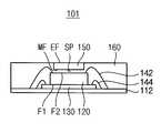
도 1을 참조하면, 반도체 패키지(101)는 기판(112), 제1 반도체 칩(120), 제1 와이어들(142) 및 방열판(150)을 포함한다. 상기 반도체 패키지(101)는 제2 반도체 칩(130) 및 제2 와이어들(144)을 더 포함할 수 있다.Referring to FIG. 1, the
상기 기판(112)은 다수의 단자들을 포함한다. 상기 단자들은 외부 장치와 전기적으로 연결될 수 있다. 상기 기판(112)은 상기 제1 와이어들(142)을 통해서 상기 제1 반도체 칩(120)과 상기 외부 장치를 전기적으로 연결시킬 수 있다.The
상기 제1 반도체 칩(120)은 상기 기판(112) 상에 배치되고, 상기 제1 와이어들(142)을 통해서 상기 기판(112)과 전기적으로 연결된다. 상기 제1 반도체 칩(120)은 제1 면(F1) 및 상기 제1 면(F1)과 대향하는 제2 면(F2)을 포함한다. 상기 제1 면(F1)은 상기 기판(112)과 마주하는 면이고, 상기 제2 면(F2)은 회로 패턴(미도시)이 형성된 활성화면이다.The
상기 제1 와이어들(142)의 일단은 상기 제2 면(F2)에 연결된다. 상기 제1 와이어들(142)의 타단은 상기 기판(112)의 상기 단자에 연결된다. 이에 따라, 상기 제1 반도체 칩(120)과 상기 기판(112)이 상기 제1 와이어들(142)을 통해서 전기적으로 연결될 수 있다.One end of the
상기 제2 반도체 칩(130)은 상기 제2 면(F2)과 상기 기판(112) 사이에 배치될 수 있다. 상기 제2 반도체 칩(130)의 활성화면이 상기 제1 면(F1)과 대향하고, 비활성화면이 상기 기판(112)과 대향한다. 평면으로 볼 때, 상기 제2 반도체 칩(130)의 면적은 상기 제1 반도체 칩(120)의 면적에 비해서 상대적으로 넓을 수 있다. 이에 따라, 상기 제2 반도체 칩(130)의 상기 활성화면은 상기 제1 반도체 칩(120)과 부분적으로 중첩되어 상기 제2 반도체 칩(130)의 상기 활성화면은 부분적으로 노출될 수 있다.The
상기 제2 반도체 칩(130)은, 상기 제2 반도체 칩(130)과 상기 기판(112) 사이에 배치된 제1 접착 부재(미도시)를 통해서 상기 기판(112) 상에 실장될 수 있다. 또한, 상기 제2 반도체 칩(130)과 상기 제1 반도체 칩(120)은 상기 제2 반도체 칩(130)의 상기 활성화면과 상기 제1 면(F1) 사이에 배치된 제2 접착 부재(미도시)를 통해서 서로 물리적으로 연결될 수 있다.The
상기 제2 와이어들(144)은 상기 제2 반도체 칩(130)을 상기 기판(112)과 전기적으로 연결시킨다. 상기 제2 반도체 칩(130)의 상기 활성화면 중에서 상기 제1 반도체 칩(120)과 중첩되지 않는 영역이 상기 제2 와이어들(144)의 일단과 연결되고, 타단이 상기 기판(112)과 연결될 수 있다.The
상기 방열판(150)은 상기 제1 반도체 칩(120)의 상기 제1 면(F1)과 마주하여 상기 제1 반도체 칩(120) 상에 배치된다. 상기 방열판(150)의 일면(이하, "몰딩면"이라 지칭하고, 도면 부호 "MF"로 나타냄)은 상기 제1 면(F1)과 이격되고, 상기 방열판(150)과 상기 제1 면(F1) 사이의 이격 공간(SP)에 상기 몰딩 부재(160)가 배치된다. 상기 방열판(150)의 타면(이하, "노출면"이라 지칭하고, 도면 부호 "EF"로 나타냄)은 상기 반도체 패키지(101)의 외부로 노출된다. 상기 이격 공간(SP)에 채워진 상기 몰딩 부재(160)에 의해서 상기 제1 반도체 칩(120)과 상기 방열판(150)이 별도의 결합 부재 없이 서로 물리적으로 연결될 수 있다.The
상기 몰딩 부재(160)는 상기 제1 반도체 칩(120)을 전체적으로 감싸고, 상기 방열판(150)을 부분적으로 몰딩한다. 즉, 상기 제1 및 제2 반도체 칩들(120, 130)과 상기 제1 및 제2 와이어들(142, 144)은 상기 몰딩 부재(160)의 내부에 몰딩되고, 상기 방열판(150)은 상기 노출면(EF)을 제외하고는 전체적으로 상기 몰딩 부재(160)의 내부에 몰딩된다. 상기 몰딩 부재(160)의 표면은 전체적으로 평탄하고, 상기 기판(112)의 표면과 평행할 수 있다. 상기 방열판(150)의 외부로 노출된 면의 표면과 상기 몰딩 부재(160)의 표면이 같은 평면 상에 배치될 수 있다.The
구체적으로, 상기 몰딩 부재(160)는 상기 제1 반도체 칩(120)의 측면들을 둘러싸면서 상기 이격 공간(SP)에까지 채워져 상기 기판(112)과 마주하는 면을 제외한 상기 제1 반도체 칩(120)을 전체적으로 몰딩한다. 또한, 상기 몰딩 부재(160)는 상기 방열판(150)의 측면들을 둘러싸면서 상기 이격 공간(SP)에까지 채워져 상기 방열판(150) 중에서 상기 방열판(150)이 상기 반도체 패키지(101)의 외부로 노출된 면을 제외한 상기 제1 반도체 칩(120)을 전체적으로 몰딩한다. 이에 따라, 상기 몰딩 부재(160)가 상기 제1 및 제2 반도체 칩들(120, 130)과 상기 제1 및 제2 와이어들(142, 144)을 보호할 수 있다.Specifically, the
상기 몰딩 부재(160)는 수지(resin)를 포함할 수 있고, 상기 몰딩 부재(160)의 구체적인 예로서는, 에폭시 몰딩 컴파운드(epoxy molding compound, EMC)를 들 수 있다.The
이하에서, 도 2a 내지 도 2e를 참조하여 도 1에 도시된 반도체 패키지의 제조 방법을 설명한다. 먼저, 도 2a를 참조하여 도 1에 도시된 반도체 패키지를 제조하기 위한 몰딩 장치의 금형을 설명한 후, 도 2b 내지 도 2e를 참조하여 도 2a에 도시된 금형을 이용하여 반도체 패키지를 제조하는 방법을 설명한다.Hereinafter, a method of manufacturing the semiconductor package shown in FIG. 1 will be described with reference to FIGS. 2A to 2E. First, a mold of the molding apparatus for manufacturing the semiconductor package shown in FIG. 1 will be described with reference to FIG. 2A, and then a method of manufacturing a semiconductor package using the mold shown in FIG. 2A will be described with reference to FIGS. 2B to 2E. Explain.
도 2a는 도 1에 도시된 반도체 패키지를 제조하기 위한 금형을 설명하기 위한 단면도이다.FIG. 2A is a cross-sectional view illustrating a mold for manufacturing the semiconductor package shown in FIG. 1.
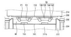
도 2a를 참조하면, 반도체 패키지를 제조하기 위한 몰딩 장치의 금형(200)은 상형(210) 및 하형(220)을 포함한다. 또한, 상기 금형(200)은 상기 상형(210)과 상기 하형(220) 사이에 배치된 중간형(230)을 더 포함할 수 있다. 도 2a에 도시된 상기 상형(210), 상기 하형(220) 및 상기 중간형(230)은 상기 몰딩 장치가 작동하지 않는 상기 금형(200)의 오픈 상태를 도시한 것이다.Referring to FIG. 2A, the
상기 상형(210)은 상부 서포트(212), 상부 플레이트(214) 및 실 부재(216)를 포함할 수 있다. 상기 상부 플레이트(214)는 상기 상부 서포트(212)의 하부면에 배치될 수 있다. 상기 상부 플레이트(214)의 상부면이 상기 상부 서포트(212)의 하부면과 접촉할 수 있고, 상기 상부 플레이트(214)의 하부면이 상기 하형(220)과 대향할 수 있다. 상기 실 부재(216)는 상기 상부 플레이트(214)의 하부면에 형성되어 상기 상형(210), 상기 중간형(230) 및 상기 하형(220)이 모두 밀착된 경우에 상기 상형(210)과 상기 중간형(230)의 간극을 막을 수 있다. 도면으로 도시하지 않았으나, 상기 상부 플레이트(214)의 하부면에는 마더 기판(110, 도 2c 참조)을 흡착하여 고정시키기 위한 진공홀들 및/또는 상기 마더 기판(110)을 파지하기 위한 홀더 등이 형성될 수 있다. 또한, 상기 진공홀들은 상기 상부 플레이트(214)의 하부면에서부터 상부면을 관통하는 흡인 배출관(미도시)과 연결될 수 있다.The
상기 하형(220)은 하부 서포트(222), 캐비티 부재(223) 및 클램핑 부재(224)를 포함할 수 있다. 상기 하부 서포트(222)는 플레이트부(221a) 및 상기 플레이트부(221a) 상에 배치된 돌출부(221b)를 포함할 수 있다. 상기 캐비티 부재(223) 및 상기 클램핑 부재(224)는 상기 플레이트부(221a) 상에 배치되고 상기 돌출부(221b)의 측면에 배치될 수 있다. 상기 하형(220)의 몰딩 공간(MP)은 상기 돌출부(221b)의 상면과 상기 캐비티 부재(223)에 의해서 정의될 수 있다. 즉, 상기 돌출부(221b)의 상면이 상기 몰딩 공간(MP)을 정의하는 바닥부가 되고 상기 캐비티 부재(223)가 상기 몰딩 공간(MP)을 정의하는 측벽면이 될 수 있다. 상기 캐비티 부재(223)는 상기 플레이트부(221a) 상에 배치된 제1 탄성 부재(225)에 연결되어 탄성적으로 지지될 수 있다. 상기 클램핑 부재(224)는 상기 캐비티 부재(223)의 외측에 배치되고, 제2 탄성 부재(226)에 연결될 수 있다. 상기 클램핑 부재(224)는 상기 제2 탄성 부재(226)에 의해서 지면과 수직한 방향으로 이동할 수 있다.The
상기 중간형(230)은 상기 상형(210)과 상기 하형(220) 사이에서 지면과 수직한 방향으로 상하 운동을 할 수 있다. 상기 중간형(230)은 상기 몰딩 공간(MP)과 대응하여 개구가 형성되어 상기 중간형(230)의 하부에서 상기 하형(220)이 삽입될 수 있다. 또한, 상기 중간형(230)의 상부에서 상기 상형(210)이 상기 중간형(230)을 누를 수 있다.The
상기 중간형(230)과 상기 하형(220) 사이에 이형 필름(300)이 배치될 수 있다. 상기 이형 필름(300)은 상기 밀봉 부재(160)를 형성한 후 상기 하형(220)으로부터 상기 밀봉 부재(160)가 용이하게 분리될 수 있도록 한다. 도면으로 도시하지 않았으나, 상기 하형(220)은 상기 이형 필름(300)이 상기 몰딩 공간(MP)으로 안정적으로 피복되도록 상기 이형 필름(300)을 흡입하는 흡입 부재를 더 포함할 수 있다.The
도 2b 내지 도 2e는 도 1에 도시된 반도체 패키지의 제조 방법을 설명하기 위한 단면도들이다.2B to 2E are cross-sectional views illustrating a method of manufacturing the semiconductor package shown in FIG. 1.
도 2a 및 도 2b를 참조하면, 상기 중간형(230)과 상기 하형(220)이 서로 밀착되어 상기 이형 필름(300)이 상기 몰딩 공간(MP)이 피복된다. 구체적으로, 상기 중간형(230)이 상기 하형(220)을 향해서 서서히 이동하고, 상기 중간형(230)이 상기 하형(220)의 상기 클램핑 부재(224)와 접촉한다. 이어서, 상기 중간형(230)과 상기 클램핑 부재(224)가 접촉된 상태에서, 상기 클램핑 부재(224)를 계속하여 가압하면 상기 제2 탄성 부재(226)에 의해서 상기 클램핑 부재(224)는 상기 캐비티 부재(230)보다 상대적으로 그 높이가 낮은 상태로 배치될 수 있다. 이때, 상기 하형(220)의 상기 흡입 부재는 상기 이형 필름(300)을 상기 중간형(230)의 이동 방향으로 흡입할 수 있다. 이에 따라, 상기 이형 필름(300)은 상기 돌출부(221b)의 상면과 상기 캐비티 부재(230)의 내측면과 직접적으로 접촉하여 상기 하형(220)에 피복될 수 있다.2A and 2B, the
이어서, 상기 이형 필름(300)이 피복된 상기 하형(220)의 상기 몰딩 공간(MP)에 상기 방열판(150)을 배치한다. 구체적으로, 상기 방열판(150)은 상기 돌출부(221b)에 피복된 상기 이형 필름(300) 상에 배치될 수 있다. 상기 몰딩 공간(MP)에는 적어도 1개 이상의 상기 방열판(150)을 배치할 수 있다. 상기 방열판(150)의 개수는 도 1에 도시된 반도체 패키지(101)의 수에 따라 임의적으로 정해질 수 있다. 서로 인접한 상기 방열판들(150)은 서로 이격되어 배치된다.Subsequently, the
상기 몰딩 공간(MP)에, 도 1에 도시된 상기 몰딩 부재(160)를 형성하는 용융된 몰딩 수지(MR)가 충진된다. 상기 몰딩 수지(MR)의 초기 높이는, 이후에 상기 중간형(230)과 밀착되어 있는 상기 하형(220)이 상기 상형(210)과 밀착될 때 상기 몰딩 공간(MP)에 패키지 단위들(SU)이 삽입된 후(도 2d 참조)의 최종 높이를 고려하여 정해질 수 있다.In the molding space MP, a molten molding resin MR, which forms the
상기에서 설명한 바와 같이, 상기 몰딩 공간(MP)에 피복된 상기 이형 필름(300) 상에 상기 방열판(150)이 배치되고, 상기 몰딩 공간(MP)에 용융된 몰딩 수지(MR)가 충진되며, 상기 하형(220) 상에 상기 상형(210)이 배치되어 있는 상태로 상기 금형(200)이 준비될 수 있다.As described above, the
한편, 상기 마더 기판(110) 상에 각각이 상기 제1 및 제2 반도체 칩들(120, 130)과 상기 제1 및 제2 와이어들(142, 144)을 포함하는 패키지 단위들(SU)을 형성한다. 상기 마더 기판(110)은 이후 공정에서 다수 개로 분리되어 도 1에 도시된 상기 반도체 패키지(101)의 상기 기판(112)을 형성할 수 있고, 상기 패키지 단위들(SU) 각각이 도 1에 도시된 상기 반도체 패키지(101)의 일부를 구성할 수 있다.Meanwhile, package units SU are formed on the
구체적으로, 상기 마더 기판(110) 상에 상기 제1 접착 부재를 이용하여 상기 제2 반도체 칩(130)을 실장하고, 상기 제2 반도체 칩(130)이 실장된 상기 마더 기판(110) 상에 상기 제2 접착 부재를 이용하여 상기 제1 반도체 칩(120)을 실장할 수 있다. 이하에서는, 상기 마더 기판(110)에서 상기 패키지 단위들(SU)이 배치된 면을 "실장면"이라고 정의한다. 상기 제1 반도체 칩(120)을 상기 마더 기판(110)과 상기 제1 와이어들(142)을 이용하여 연결시키고, 상기 제2 반도체 칩(130)을 상기 제2 와이어들(144)을 이용하여 상기 마더 기판(110)과 연결시킬 수 있다.Specifically, the
상기 패키지 단위들(SU)이 실장된 상기 마더 기판(110)을 제조한 후, 상기 마더 기판(110)의 상기 실장면의 대향면을, 상기 상형(210)의 상기 상부 다이(214)의 하부면에 배치시킨다. 상기 패키지 단위들(SU)이 실장된 상기 마더 기판(110)은 상기 상부 다이(214)의 상기 진공홀들에 의해서 상기 상부 다이(214)에 안정적으로 배치될 수 있다. 상기 마더 기판(110)에 실장된 상기 패키지 단위들(SU)은 상기 몰딩 공간(MP)에 놓인 상기 방열판들(150)과 일대일 대응되도록 배치될 수 있다.After manufacturing the
도 2c를 참조하면, 상기 중간형(230)과 밀착되어 있는 상기 하형(220)을 서서히 상기 상형(210)을 향해 이동시킨다. 이에 따라, 상기 마더 기판(110)에 실장된 상기 패키지 단위들(SU)이 상기 몰딩 공간(MP)에 배치됨으로써, 상기 마더 기판(110)에 실장된 상기 패키지 단위들(SU)은 상기 몰딩 수지(MR)를 헤치면서 상기 돌출부(221b)의 상면을 향해서 서서히 이동할 수 있다. 구체적으로, 상기 제1 반도체 칩(120)의 상기 제2 면(F2)이 서서히 상기 방열판(150)을 향해 이동할 수 있다.Referring to FIG. 2C, the
도 2d를 참조하면, 상기 중간형(230)과 밀착되어 있는 상기 하형(220)이, 상기 상형(210)과 밀착된다. 이때, 상기 상형(210)의 상기 실 부재(216)가 상기 중간형(230)과 직접적으로 접촉할 수 있다. 즉, 상기 실 부재(216)는 상기 상형(210)과 상기 중간형(230)의 간극을 막을 수 있다.Referring to FIG. 2D, the
상기 하형(220), 상기 중간형(230) 및 상기 상형(210)이 모두 밀착된 상태에서, 상기 제1 반도체 칩(120)의 상기 제2 면(F2)은 상기 방열판(150)의 상기 몰딩면(MF)과 마주하되, 소정 간격으로 이격되어 배치된다. 상기 제2 면(F2)과 상기 몰딩면(MF) 사이의 이격 공간(SP)에는 상기 몰딩 수지(MR)가 채워져, 상기 제2 면(F2)과 상기 몰딩면(MF) 사이에 상기 몰딩 수지(MR)가 개재될 수 있다.In a state where the
이어서, 상기 몰딩 수지(MR)를 경화시킴으로써 상기 몰딩면(MF)과 상기 제2 면(F2) 사이의 경화된 상기 몰딩 수지(MR)에 의해서 상기 방열판(150)과 상기 제1 반도체 칩(120)이 연결된다. 상기 패키지 단위들(SU)은 상기 몰딩 수지(MR)가 경화됨에 따라 형성되는 상기 몰딩 부재(160)에 의해서 몰딩된다. 또한, 상기 방열판들(150) 각각의 측면들과 상기 몰딩면(MF)이 상기 몰딩 부재(160)에 의해서 몰딩될 수 있다. 즉, 상기 몰딩 수지(MR)를 경화시킴으로써 상기 마더 기판(110) 상에 상기 몰딩 부재(160)가 형성될 수 있다. 상기 마더 기판(110)의 실장면의 표면에서부터 상기 이형 필름(300)의 표면까지의 거리인 상기 몰딩 부재(160)의 전체 높이는 상기 금형(200)의 깊이에 의존할 수 있다.Subsequently, the
상기 몰딩 부재(160)가 형성된 후, 상기 상형(210)과 상기 하형(220)을 분리시킨다. 구체적으로, 상기 상형(210)을 상기 중간형(230)과 밀착된 상기 하형(220)과 분리시킬 수 있다. 이때, 상기 몰딩 부재(160)가 형성된 상기 마더 기판(110)은 상기 상형(210)에 붙어 있는 상태로 유지된다. 도 2e를 참조하면, 상기 상형(210)으로부터 상기 몰딩 부재(160)가 형성된 상기 마더 기판(110)을 분리시킨다. 이에 따라, 상기 몰딩 부재(160)가 형성된 상기 마더 기판(110)이 상기 금형(200)으로부터 분리된다.After the
상기 금형(200)으로부터 상기 마더 기판(110)을 분리시키면, 상기 이형 필름(300)의 표면에 상기 몰딩 부재(160)의 표면과 상기 방열판(150)의 상기 노출면(EF)이 접촉되기 때문에 상기 몰딩 부재(160)의 표면과 상기 노출면(EF)의 표면이 서로 동일 평면 상에 배치될 수 있다. 이에 따라, 상기 몰딩 부재(160)가 상기 노출면(EF)에 비해서 상대적으로 돌출되거나 함입되는 부분이 없이 상기 노출면(EF)과 함께 평평한 면을 만들기 때문에 별도의 표면 연마 공정이 수반될 필요가 없다.When the
이어서, 상기 금형(200)으로부터 분리된 상기 마더 기판(110)을 제1, 제2 및 제3 커팅 라인들(CL1, CL2, CL3)을 따라 절단하여 도 1에 도시된 다수의 상기 반도체 패키지들(101)을 제조할 수 있다. 즉, 상기 마더 기판(110)이 상기 절단 공정을 통해서 도 1에 도시된 다수의 상기 기판들(112)로 분리될 수 있고, 상기 기판들(112) 각각 상에 상기 제1 및 제2 반도체 칩들(120, 130)과 상기 제1 및 제2 와이어들(142, 144), 상기 방열판(150) 및 상기 몰딩 부재(160)가 배치될 수 있다.Subsequently, the
상기에서 설명한 바에 따르면, 상기 제1 반도체 칩(120)을 상기 방열판(150)과 별도의 결합 부재 없이 상기 몰딩 부재(160)를 이용하여 상기 몰딩 부재(160)만으로 결합시킬 수 있다. 또한, 상기 몰딩 부재(160)를 형성하는 공정에서 상기 제1 반도체 칩(120)과 상기 방열판(150)이 결합되므로 추가적인 공정도 수반되지 않는다. 뿐만 아니라, 상기 방열판들(150)과 상기 패키지 단위들(SU) 사이의 거리를 상기 마더 기판(110)의 전면에서 일정하게 유지할 수 있기 때문에 이에 의해 제조되는 모든 반도체 패키지들(101)의 전체 높이를 균일하게 관리할 수 있고, 상기 방열판(150)의 두께가 약 100㎛ 미만으로 매우 얇더라도 이미 상기 금형(200) 상에 놓인 상태에서 상기 방열판(150)과 상기 패키지 단위들(SU)이 결합될 수 있으므로 용이하게 결합시킬 수 있다. 나아가, 상기 몰딩 부재(160)의 표면과 상기 방열판(150)의 상기 노출면(EF)의 표면을 연마하거나 세정하는 공정 또한 생략될 수 있다. 이에 따라, 상기 반도체 패키지(101)의 제조 공정 수를 감소시키고, 제조에 소요되는 시간을 감소시킴으로써 생산성을 향상시킬 수 있다.As described above, the
도 1에서는 상기 반도체 패키지(101)가 제1 및 제2 반도체 칩들(120, 130)을 포함하는 것을 도시하고 있으나, 상기 제2 반도체 칩(130)은 생략될 수 있다. 이와 달리, 상기 반도체 패키지(101)는 상기 제1 반도체 칩(120)과 상기 방열판(150) 사이에 형성된 제3 반도체 칩을 더 포함할 수 있고, 이때, 상기 제3 반도체 칩은 상기 방열판(150)과 이격되고 그 사이에 상기 몰딩 부재(160)의 일부가 채워질 수 있다.In FIG. 1, the
또한, 도 2b 내지 도 2e에서는 도 2a에 도시된 금형(200)을 이용하여 상기 반도체 패키지(101)를 제조하는 것을 설명하였으나, 본 발명의 반도체 패키지(101)를 제조하는데 이용되는 금형은 도 2a에 도시된 것에 한정되지 않고 다양한 종류의 컴프레션 몰드(compression mold) 방식을 수행할 수 있는 금형들을 이용할 수 있다.2B to 2E illustrate manufacturing the
도 3은 본 발명의 다른 실시예에 따라 제조된 반도체 패키지의 단면도이다.3 is a cross-sectional view of a semiconductor package manufactured according to another embodiment of the present invention.
도 3에 도시된 반도체 패키지(102)는, 버퍼 필름(BL)을 더 포함하고 상기 버퍼 필름(BL)이 방열판(150) 및 제1 반도체 칩(120)과 각각 접촉하는 것을 제외하고는 도 1에서 설명한 반도체 패키지(101)와 실질적으로 동일하다. 따라서, 중복되는 설명은 생략한다.The
도 3을 참조하면, 반도체 패키지(102)는 기판(112) 상에 형성된 제1 반도체 칩(120), 상기 기판(112)과 상기 제1 반도체 칩(120) 사이에 배치된 제2 반도체 칩(130), 상기 제1 반도체 칩(120)을 상기 기판(112)과 전기적으로 연결하는 제1 와이어들(142), 상기 제2 반도체 칩(130)을 상기 기판(112)과 전기적으로 연결하는 제2 와이어들(144), 방열판(150), 버퍼 필름(BL) 및 몰딩 부재(160)를 포함한다.Referring to FIG. 3, the
상기 버퍼 필름(BL)은 상기 제1 반도체 칩(120)의 활성화면과 상기 방열판(150)의 몰딩면(MF) 사이에 배치되고, 상기 버퍼 필름(BL)이 상기 활성화면 및 상기 몰딩면(MF) 각각과 접촉한다. 상기 버퍼 필름(BL)에 의해서 상기 제1 반도체 칩(120)과 상기 방열판(150)이 물리적으로 연결될 수 있다. 또한, 상기 버퍼 필름(BL)은 상기 활성화면을 보호할 수 있고, 상기 제1 와이어(142)와 상기 방열판(150)이 접촉하는 것을 방지할 수 있다.The buffer film BL is disposed between the activation surface of the
도 4는 도 3에 도시된 반도체 패키지의 제조 방법을 설명하기 위한 단면도이다.4 is a cross-sectional view illustrating a method of manufacturing the semiconductor package shown in FIG. 3.
도 3에 도시된 반도체 패키지는 도 2a에서 설명한 금형(200)을 이용하여 제조할 수 있다. 따라서, 도 3에 도시된 반도체 패키지를 제조하는데 이용되는 금형은 도 2a를 참조하여 설명하고 중복되는 상세한 설명은 생략한다.The semiconductor package illustrated in FIG. 3 may be manufactured using the
도 4를 도 2a 및 도 3과 함께 참조하면, 먼저 마더 기판(110) 상에 다수의 패키지 단위들(SU)을 형성하고 상기 마더 기판(110)을 금형(200)과 결합시킨다. 상기 금형(200)은 이형 필름(300)에 의해서 하형(220)이 피복된 상태를 갖는다. 상기 이형 필름(300)에 의해 피복된 상기 하형(220)의 몰딩 공간(MP)에 상기 방열판(150) 및 상기 버퍼 필름(BL)이 순차적으로 적층한다. 이어서, 상기 몰딩 공간에 용융된 몰딩 수지(MR)를 충진한다. 상기 방열판(150)과 상기 버퍼 필름(BL)은 상기 패키지 단위들(SU) 각각과 대응되도록 배치된다. 서로 인접한 상기 방열판들(150)은 서로 이격되어 배치된다.Referring to FIG. 4 together with FIGS. 2A and 3, first, a plurality of package units SU are formed on a
상기 금형(200)의 중간형(230)과 밀착된 상기 하형(220)과, 상기 패키지 단위들(SU)이 실장된 상기 마더 기판(110)이 배치된 상형(210)을 밀착시키면, 상기 제1 반도체 칩(120)의 상기 활성화면이 상기 버퍼 필름(BL)의 일면과 접촉한다. 상기 몰딩 공간(MP)의 깊이는 상기 중간형(230)과 밀착된 상기 하형(220)과, 상기 상형(210)을 밀착시킬 때 상기 버퍼 필름(BL)과 상기 활성화면이 접촉하도록 상기 패키지 단위들(SU) 각각의 두께와 상기 방열판(150) 및 상기 버퍼 필름(BL)의 전체 두께를 고려하여 정해진다.When the
상기 상형(210), 상기 하형(220) 및 상기 중간형(230)이 모두 밀착된 상태에서, 상기 몰딩 수지(MR)를 경화시킨다. 이어서, 상기 마더 기판(110)을 상기 금형(200)으로부터 분리시킨 후, 상기 마더 기판(110)을 커팅하여 도 3에 도시된 상기 반도체 패키지(102)를 다수 개 제조할 수 있다.The molding resin MR is cured while the
상기에서 설명한 바에 따르면, 모든 반도체 패키지들(102)의 전체 높이를 균일하게 관리할 수 있고, 상기 방열판(150)의 두께가 약 100㎛ 미만으로 매우 얇더라도 상기 패키지 단위들(SU)과 상기 방열판(150)을 용이하게 결합시킬 수 있다. 나아가, 상기 몰딩 부재(160)의 표면과 상기 방열판(150)의 상기 노출면(EF)의 표면을 연마하거나 세정하는 공정 또한 생략될 수 있다. 이에 따라, 상기 반도체 패키지(102)의 제조 공정 수를 감소시키고, 제조에 소요되는 시간을 감소시킴으로써 생산성을 향상시킬 수 있다.As described above, the overall height of all the semiconductor packages 102 may be uniformly managed, and even if the thickness of the
도 3에서는 상기 방열판(150) 및 상기 버퍼 필름(BL)의 면적이 상기 활성화면의 면적보다 좁은 경우를 일례로 도시하였으나, 상기 방열판(150)의 면적이 넓을수록 상기 반도체 패키지(102)의 방열 특성이 향상될 수 있으므로, 상기 방열판(150)이 상기 활성화면의 면적과 실질적으로 동일하거나 더 넓을 수 있다. 다만, 상기 방열판(150)의 면적이 상기 활성화면의 면적보다 넓은 경우, 상기 제1 와이어들(142)이 상기 활성화면과 접촉하여 전기적으로 쇼트될 가능성이 있으나 상기 버퍼 필름(BL)이 상기 방열판(150)의 면적과 실질적으로 동일하게 상기 방열판(150)을 커버하고 있으므로 상기 제1 와이어들(142)과 상기 활성화면 사이의 쇼트를 방지할 수 있다. 이때, 상기 버퍼 필름(BL)의 두께는 도 3에 도시된 것과 달리 상기 방열판(150)의 두께보다 두꺼운 것이 바람직하다.3 illustrates an example in which the areas of the
도 5는 본 발명의 또 다른 실시예에 따라 제조된 반도체 패키지의 단면도이다.5 is a cross-sectional view of a semiconductor package manufactured according to another embodiment of the present invention.
도 5에 도시된 반도체 패키지(103)는 버퍼 필름(BL) 및 방열판(150)의 면적이 기판(112)의 면적과 실질적으로 동일한 것을 제외하고는 도 3에서 설명한 반도체 패키지(102)와 실질적으로 동일하다. 따라서 중복되는 설명은 생략한다.The
도 5를 참조하면, 반도체 패키지(103)는 기판(112) 상에 형성된 제1 및 제2 반도체 칩들(120, 130), 제1 및 제2 와이어들(142, 144), 방열판(150), 버퍼 필름(BL) 및 몰딩 부재(160)를 포함한다.Referring to FIG. 5, the
상기 버퍼 필름(BL) 및 상기 방열판(150) 각각의 면적은 실질적으로 서로 동일하고, 상기 기판(112)의 면적 또한 상기 버퍼 필름(BL) 및 상기 방열판(150)의 면적과 실질적으로 동일하다. 예를 들어, 상기 기판(112)의 제1 너비(W1)는 상기 버퍼 필름(BL) 및 상기 방열판(150)의 제2 너비(W2)와 실질적으로 동일할 수 있다.The area of each of the buffer film BL and the
상기 버퍼 필름(BL)이 상기 방열판(150)과 상기 제1 와이어들(142)이 전기적으로 쇼트되는 것을 방지할 수 있다. 또한, 상기 버퍼 필름(BL)이 상기 제1 반도체 칩(120)과 상기 방열판(150)을 물리적으로 연결시킬 수 있다. 상기 몰딩 부재(160)에 의해서 상기 제1 및 제2 반도체 칩들(120, 130), 상기 버퍼 필름(BL) 및 상기 방열판(150)의 일부가 몰딩될 수 있다.The buffer film BL may prevent the
도 6a 및 도 6b는 도 5에 도시된 반도체 패키지의 제조 방법을 설명하기 위한 단면도들이다.6A and 6B are cross-sectional views illustrating a method of manufacturing the semiconductor package shown in FIG. 5.
도 5에 도시된 반도체 패키지는 도 2a에서 설명한 금형(200)을 이용하여 제조할 수 있다. 따라서, 도 5에 도시된 반도체 패키지를 제조하는데 이용되는 금형은 도 2a를 참조하여 설명하고 중복되는 상세한 설명은 생략한다.The semiconductor package illustrated in FIG. 5 may be manufactured using the
도 2a 및 도 5와 함께, 도 6a를 참조하면, 마더 기판(110) 상에 다수의 패키지 단위들(SU)을 실장한다. 이어서, 도 2a에 도시된 금형(200)의 하형(220)을 이형 필름(300)으로 피복시키고, 상기 금형(200)의 상형(210)에 상기 패키지 단위들(SU)이 실장된 상기 마더 기판(110)을 배치시킨다. 상기 하형(220)의 몰딩 공간(MP)을 피복하고 있는 상기 이형 필름(300) 상에 방열층(PL1) 및 버퍼층(PL2)을 순차적으로 적층시킬 수 있다. 상기 방열층(PL1)은 금속층으로서, 절단되어 도 5에 도시된 상기 방열판(150)을 형성한다. 상기 버퍼층(PL2)은 수지층으로서, 절단되어 도 5에 도시된 상기 버퍼 필름(BL)을 형성한다.Referring to FIG. 6A together with FIGS. 2A and 5, a plurality of package units SU are mounted on a
상기 방열층(PL1) 및 상기 버퍼층(PL2)은 상기 하형(220)의 하부 플레이트(222)의 돌출부(221a)의 상면에 전체적으로 형성될 수 있다. 이어서, 상기 몰딩 공간(MP)에 용융된 몰딩 수지(MR)를 충진시킨다. 상기 몰딩 수지(MR)가 상기 방열층(PL1) 및 상기 버퍼층(PL2)을 덮는다.The heat dissipation layer PL1 and the buffer layer PL2 may be formed on the entire surface of the
도 2a에 도시된 금형(200)의 상기 상형(210), 상기 하형(220) 및 상기 중간형(230)이 밀착되면, 상기 제1 반도체 칩(120)의 활성화면이 상기 버퍼층(PL2)의 일면과 접촉한다. 이 상태로, 상기 몰딩 수지(MR)를 경화시킨 후에 상기 상형(210)과 상기 하형(220)을 분리시키고, 상기 상형(210)으로부터 상기 마더 기판(110)을 떼어낸다.When the
도 6b를 참조하면, 상기 금형(200)으로부터 분리된 상기 마더 기판(110)을 상기 패키지 단위들(SU) 별로 제1, 제2 및 제3 커팅 라인들(CL1, CL2, CL3)을 따라 커팅하여 도 5에 도시된 다수의 상기 반도체 패키지들(103)을 제조할 수 있다. 이에 따라, 상기 방열층(PL1) 및 상기 버퍼층(PL2)의 절단면들은 상기 기판(112)의 절단면과 실질적으로 동일하고, 상기 버퍼 필름(BL) 및 상기 방열판(150) 각각의 면적이 상기 기판(112)의 면적과 실질적으로 동일할 수 있다. 즉, 상기 방열층(PL1), 상기 버퍼층(PL2) 및 상기 마더 기판(110)이 모두 동일한 절단면을 갖기 때문에, 상기 기판(112)의 제1 너비(W1)는 상기 버퍼 필름(BL) 및 상기 방열판(150)의 제2 너비(W2)와 실질적으로 동일할 수 있다.Referring to FIG. 6B, the
상기에서 설명한 바에 따르면, 상기 반도체 패키지들(103)의 제조 공정수를 줄일 수 있다. 또한, 이미 서로 분리된 상태의 금속 패턴들과 버퍼 패턴들을 상기 바닥부(210)에 배치시키는 경우에 비해서, 상기 바닥부(210)에 전체적으로 형성된 상기 방열층(PL1) 및 상기 버퍼층(PL2)을 이용하고 이를 절단하여 상기 방열판(150) 및 상기 버퍼 필름(BL)을 형성함으로써 상기 패키지 단위들(SU)과 상기 금형(200)의 얼라인을 자유롭게 할 수 있다. 이에 따라, 공정의 신뢰성이 향상될 수 있다.As described above, the number of manufacturing processes of the semiconductor packages 103 may be reduced. In addition, the heat dissipation layer PL1 and the buffer layer PL2 formed on the
이상에서는 실시예들을 참조하여 설명하였지만, 해당 기술 분야의 숙련된 당업자는 하기의 특허 청구의 범위에 기재된 본 발명의 사상 및 영역으로부터 벗어나지 않는 범위 내에서 본 발명을 다양하게 수정 및 변경시킬 수 있음을 이해할 수 있을 것이다.It will be apparent to those skilled in the art that various modifications and variations can be made in the present invention without departing from the spirit or scope of the present invention as defined by the following claims. You will understand.
본 발명에 따른 반도체 패키지 및 이의 제조 방법은 반도체 칩과 방열판이 별도의 결합 부재 없이 몰딩 부재에 의해서 결합시킬 수 있다. 이에 따라, 상기 방열판을 상기 반도체 칩과 결합시키는 별도의 공정이 필요 없으므로 상기 반도체 패키지의 제조 원가를 감소시킬 수 있다.In the semiconductor package and the method of manufacturing the same according to the present invention, the semiconductor chip and the heat sink may be coupled by the molding member without a separate coupling member. Accordingly, since a separate process of combining the heat sink with the semiconductor chip is not required, the manufacturing cost of the semiconductor package can be reduced.
또한, 상기 방열판과 상기 반도체 칩 사이의 거리를 일정하게 유지할 수 있어 제조되는 모든 반도체 패키지들의 전체 높이를 균일하게 관리할 수 있고, 상기 방열판의 두께가 약 100㎛ 미만이더라도 용이하게 상기 반도체 칩과 결합시킬 수 있다. 따라서, 상기 반도체 패키지의 제조 신뢰성을 향상시킬 수 있다.In addition, the distance between the heat sink and the semiconductor chip can be kept constant so that the overall height of all manufactured semiconductor packages can be managed uniformly, and easily coupled with the semiconductor chip even if the thickness of the heat sink is less than about 100 μm. You can. Therefore, manufacturing reliability of the semiconductor package can be improved.
나아가, 상기 방열판과 상기 반도체 칩을 결합시킨 후에 별도의 세정 공정이나 처리 공정을 요하지 않기 때문에 상기 반도체 패키지의 제조 공정 수를 감소시킬 수 있다. 이에 따라, 상기 반도체 패키지의 제조에 소요되는 시간을 감소시킴으로써 생산성을 향상시킬 수 있다.Furthermore, since no separate cleaning process or processing is required after the heat sink and the semiconductor chip are combined, the number of manufacturing steps of the semiconductor package can be reduced. Accordingly, productivity can be improved by reducing the time required for manufacturing the semiconductor package.
101, 102, 103: 반도체 패키지112: 기판
120, 130: 제1, 제2 반도체 칩
142, 144: 제1, 제2 와이어
150: 방열판160: 몰딩 부재
F1, F2: 제1, 제2 면MF: 몰딩면
EF: 노출면110: 마더 기판
200: 금형300: 이형 필름
SU: 패키지 단위SP: 이격 공간
BL: 버퍼 필름210: 상형
PL1, PL2: 제1, 제2 마더층220: 하형
CL1, CL2, CL3: 제1, 제2, 제3 커팅 라인230: 중간형101, 102, 103: semiconductor package 112: substrate
120 and 130: first and second semiconductor chips
142, 144: first and second wire
150: heat sink 160: molding member
F1, F2: 1st, 2nd surface MF: Molding surface
EF: Exposed surface 110: Mother board
200: mold 300: release film
SU: Package Unit SP: Spacing Space
BL: Buffer Film 210: Pictograph
PL1, PL2: First and second mother layers 220: Lower mold
CL1, CL2, CL3: 1st, 2nd, 3rd cutting line 230: Intermediate
Claims (10)
Translated fromKorean상기 방열판이 배치된 상기 몰딩 공간에 용융된 몰딩 수지를 충진하는 단계;
기판에 실장된 반도체 칩이 상기 몰딩 수지에 잠기도록 상기 몰딩 공간에 배치하는 단계;
상기 몰딩 수지를 경화시켜, 상기 방열판 및 상기 반도체 칩을 일체로 고정하되 상기 방열판의 일부가 외부로 노출되도록 몰딩 부재를 형성하는 단계; 및
상기 몰딩 부재가 형성된 기판을 상기 금형으로부터 분리하는 단계를 포함하고,
상기 몰딩 수지를 충진하기 전에, 상기 몰딩 공간에 배치된 방열판 상에 버퍼 필름을 배치시키는 단계를 더 포함하며, 상기 버퍼 필름은 상기 방열판 및 상기 반도체 칩 각각과 접촉하는 것을 특징으로 하는 반도체 패키지의 제조 방법.Arranging a heat sink in a molding space of a mold covered with a release film;
Filling a molten molding resin into the molding space in which the heat sink is disposed;
Disposing a semiconductor chip mounted on a substrate in the molding space to be immersed in the molding resin;
Curing the molding resin to form a molding member to integrally fix the heat sink and the semiconductor chip, but to expose a part of the heat sink to the outside; And
Separating the substrate on which the molding member is formed from the mold;
Before filling the molding resin, the method further comprises disposing a buffer film on a heat sink disposed in the molding space, wherein the buffer film is in contact with each of the heat sink and the semiconductor chip. Way.
상기 방열판과 상기 반도체 칩은 서로 마주하고 이격되어 상기 몰딩 수지가 상기 방열판과 상기 반도체 칩 사이에 채워지는 것을 특징으로 하는 반도체 패키지의 제조 방법.The method of claim 4, wherein in the molding space,
And the heat sink and the semiconductor chip face each other and are spaced apart from each other so that the molding resin is filled between the heat sink and the semiconductor chip.
상기 방열층이 배치된 상기 몰딩 공간에 몰딩 수지를 충진하는 단계;
마더 기판에 실장된 적어도 2 이상의 반도체 칩들이 상기 몰딩 수지에 잠기도록 상기 몰딩 공간에 배치시키는 단계;
상기 몰딩 수지를 경화시켜, 상기 방열층 및 상기 반도체 칩들을 일체로 고정하되 상기 방열층의 일부가 외부로 노출되도록 몰딩 부재를 형성하는 단계;
상기 몰딩 부재가 형성된 마더 기판을 상기 금형으로부터 분리시키는 단계; 및
상기 금형으로부터 분리된 마더 기판을 커팅하여, 상기 반도체 칩들 각각과 마주하는 다수의 방열판들을 형성하는 단계를 포함하는 반도체 패키지의 제조 방법.Disposing a heat dissipation layer in a molding space of a mold covered with a release film;
Filling a molding resin into the molding space in which the heat dissipation layer is disposed;
Placing at least two semiconductor chips mounted on a mother substrate in the molding space to be immersed in the molding resin;
Curing the molding resin to form the molding member so that the heat dissipation layer and the semiconductor chips are integrally fixed and a part of the heat dissipation layer is exposed to the outside;
Separating the mother substrate on which the molding member is formed from the mold; And
Cutting the mother substrate separated from the mold to form a plurality of heat sinks facing each of the semiconductor chips.
상기 반도체 칩들 각각의 면적보다 넓거나 동일한 것을 특징으로 하는 반도체 패키지의 제조 방법.The method of claim 8, wherein the area of each of the heat sink is
A method of manufacturing a semiconductor package, characterized in that it is larger than or equal to the area of each of the semiconductor chips.
상기 방열판들을 형성하는 단계에서 상기 버퍼층이 커팅되어 상기 반도체 칩들 각각과 마주하고 상기 방열판들 각각 상에 배치된 다수의 버퍼 필름들을 형성하는 것을 특징으로 하는 반도체 패키지의 제조 방법.The method of claim 8, further comprising forming a buffer layer on the heat dissipation layer disposed in the molding space before filling the molding resin.
And forming a plurality of buffer films facing the semiconductor chips and disposed on each of the heat sinks in the step of forming the heat sinks.
Priority Applications (1)
| Application Number | Priority Date | Filing Date | Title |
|---|---|---|---|
| KR1020100133395AKR101238212B1 (en) | 2010-12-23 | 2010-12-23 | Semiconductor package and method for manufacturing the same |
Applications Claiming Priority (1)
| Application Number | Priority Date | Filing Date | Title |
|---|---|---|---|
| KR1020100133395AKR101238212B1 (en) | 2010-12-23 | 2010-12-23 | Semiconductor package and method for manufacturing the same |
Publications (2)
| Publication Number | Publication Date |
|---|---|
| KR20120071734A KR20120071734A (en) | 2012-07-03 |
| KR101238212B1true KR101238212B1 (en) | 2013-02-28 |
Family
ID=46706663
Family Applications (1)
| Application Number | Title | Priority Date | Filing Date |
|---|---|---|---|
| KR1020100133395AExpired - Fee RelatedKR101238212B1 (en) | 2010-12-23 | 2010-12-23 | Semiconductor package and method for manufacturing the same |
Country Status (1)
| Country | Link |
|---|---|
| KR (1) | KR101238212B1 (en) |
Cited By (1)
| Publication number | Priority date | Publication date | Assignee | Title |
|---|---|---|---|---|
| US11581234B2 (en) | 2019-06-07 | 2023-02-14 | Samsung Electronics Co., Ltd. | Semiconductor package with improved heat dissipation |
Families Citing this family (1)
| Publication number | Priority date | Publication date | Assignee | Title |
|---|---|---|---|---|
| TWI560619B (en)* | 2016-03-01 | 2016-12-01 | Chipmos Technologies Inc | Manufacturing method and manufacturing apparatus of fingerprint identification chip package structure |
Citations (4)
| Publication number | Priority date | Publication date | Assignee | Title |
|---|---|---|---|---|
| JPH09232475A (en)* | 1996-02-22 | 1997-09-05 | Nitto Denko Corp | Semiconductor device and manufacturing method thereof |
| KR20000003753A (en)* | 1998-06-29 | 2000-01-25 | 김영환 | Stack package and method thereof |
| KR20070117986A (en)* | 2006-06-09 | 2007-12-13 | 후지쯔 가부시끼가이샤 | Semiconductor device, manufacturing method thereof and mounting method thereof |
| KR20100126910A (en)* | 2009-05-25 | 2010-12-03 | 세크론 주식회사 | Electronic component molding method and electronic component molding device |
- 2010
- 2010-12-23KRKR1020100133395Apatent/KR101238212B1/ennot_activeExpired - Fee Related
Patent Citations (4)
| Publication number | Priority date | Publication date | Assignee | Title |
|---|---|---|---|---|
| JPH09232475A (en)* | 1996-02-22 | 1997-09-05 | Nitto Denko Corp | Semiconductor device and manufacturing method thereof |
| KR20000003753A (en)* | 1998-06-29 | 2000-01-25 | 김영환 | Stack package and method thereof |
| KR20070117986A (en)* | 2006-06-09 | 2007-12-13 | 후지쯔 가부시끼가이샤 | Semiconductor device, manufacturing method thereof and mounting method thereof |
| KR20100126910A (en)* | 2009-05-25 | 2010-12-03 | 세크론 주식회사 | Electronic component molding method and electronic component molding device |
Cited By (2)
| Publication number | Priority date | Publication date | Assignee | Title |
|---|---|---|---|---|
| US11581234B2 (en) | 2019-06-07 | 2023-02-14 | Samsung Electronics Co., Ltd. | Semiconductor package with improved heat dissipation |
| US12341074B2 (en) | 2019-06-07 | 2025-06-24 | Samsung Electronics Co., Ltd. | Semiconductor package with increased thermal dissipation |
Also Published As
| Publication number | Publication date |
|---|---|
| KR20120071734A (en) | 2012-07-03 |
Similar Documents
| Publication | Publication Date | Title |
|---|---|---|
| KR101536045B1 (en) | Fan-Out Wafer Level Package Structure | |
| TWI377658B (en) | Integrated circuit package system with leadframe array | |
| CN107026107A (en) | The manufacture device and manufacture method and electronic unit of electronic unit | |
| TW202029858A (en) | System-in-package, interposer and method of assembly of a system-in-package | |
| US10177067B2 (en) | Manufacturing method of package carrier | |
| US20070132077A1 (en) | Flip chip MLP with conductive ink | |
| KR20140141474A (en) | Semiconductor device | |
| US20130334677A1 (en) | Semiconductor Modules and Methods of Formation Thereof | |
| US9620438B2 (en) | Electronic device with heat dissipater | |
| CN102610533B (en) | Injection sealing system and method thereof | |
| KR20130022821A (en) | Stacked package and method of manufacturing the same | |
| KR101238212B1 (en) | Semiconductor package and method for manufacturing the same | |
| US20090315171A1 (en) | Pin substrate and package | |
| CN101814461B (en) | Packaging substrate structure, chip packaging structure and manufacturing method thereof | |
| JPWO2020129273A1 (en) | Semiconductor devices and methods for manufacturing semiconductor devices | |
| US9318356B2 (en) | Substrate strip | |
| KR20160091810A (en) | Semiconductor device | |
| KR101261483B1 (en) | Method for manufacturing semiconductor package | |
| CN103219244B (en) | System-in-package structure for semiconductor package | |
| CN102751203A (en) | Semiconductor package structure and manufacturing method thereof | |
| JP5247668B2 (en) | Semiconductor package manufacturing apparatus and semiconductor package manufacturing method | |
| TW202027236A (en) | Packaging structure for reducing residual air and method thereof capable of effectively preventing the chip module package from electrical connection failure | |
| KR100818530B1 (en) | Manufacturing method of semiconductor package mold and semiconductor chip package | |
| JP2008112929A (en) | Circuit device, and manufacturing method of the same | |
| US20130181343A1 (en) | Multi-chip package and method of manufacturing the same |
Legal Events
| Date | Code | Title | Description |
|---|---|---|---|
| A201 | Request for examination | ||
| PA0109 | Patent application | St.27 status event code:A-0-1-A10-A12-nap-PA0109 | |
| PA0201 | Request for examination | St.27 status event code:A-1-2-D10-D11-exm-PA0201 | |
| D13-X000 | Search requested | St.27 status event code:A-1-2-D10-D13-srh-X000 | |
| D14-X000 | Search report completed | St.27 status event code:A-1-2-D10-D14-srh-X000 | |
| PE0902 | Notice of grounds for rejection | St.27 status event code:A-1-2-D10-D21-exm-PE0902 | |
| PG1501 | Laying open of application | St.27 status event code:A-1-1-Q10-Q12-nap-PG1501 | |
| E13-X000 | Pre-grant limitation requested | St.27 status event code:A-2-3-E10-E13-lim-X000 | |
| P11-X000 | Amendment of application requested | St.27 status event code:A-2-2-P10-P11-nap-X000 | |
| P13-X000 | Application amended | St.27 status event code:A-2-2-P10-P13-nap-X000 | |
| R17-X000 | Change to representative recorded | St.27 status event code:A-3-3-R10-R17-oth-X000 | |
| PN2301 | Change of applicant | St.27 status event code:A-3-3-R10-R13-asn-PN2301 St.27 status event code:A-3-3-R10-R11-asn-PN2301 | |
| E701 | Decision to grant or registration of patent right | ||
| PE0701 | Decision of registration | St.27 status event code:A-1-2-D10-D22-exm-PE0701 | |
| GRNT | Written decision to grant | ||
| PR0701 | Registration of establishment | St.27 status event code:A-2-4-F10-F11-exm-PR0701 | |
| PR1002 | Payment of registration fee | St.27 status event code:A-2-2-U10-U11-oth-PR1002 Fee payment year number:1 | |
| PG1601 | Publication of registration | St.27 status event code:A-4-4-Q10-Q13-nap-PG1601 | |
| FPAY | Annual fee payment | Payment date:20160205 Year of fee payment:4 | |
| PR1001 | Payment of annual fee | St.27 status event code:A-4-4-U10-U11-oth-PR1001 Fee payment year number:4 | |
| R17-X000 | Change to representative recorded | St.27 status event code:A-5-5-R10-R17-oth-X000 | |
| PN2301 | Change of applicant | St.27 status event code:A-5-5-R10-R13-asn-PN2301 St.27 status event code:A-5-5-R10-R11-asn-PN2301 | |
| LAPS | Lapse due to unpaid annual fee | ||
| PC1903 | Unpaid annual fee | St.27 status event code:A-4-4-U10-U13-oth-PC1903 Not in force date:20170223 Payment event data comment text:Termination Category : DEFAULT_OF_REGISTRATION_FEE | |
| PC1903 | Unpaid annual fee | St.27 status event code:N-4-6-H10-H13-oth-PC1903 Ip right cessation event data comment text:Termination Category : DEFAULT_OF_REGISTRATION_FEE Not in force date:20170223 |