KR101229019B1 - Liquid crystal display device and driving circuit of the same - Google Patents
Liquid crystal display device and driving circuit of the sameDownload PDFInfo
- Publication number
- KR101229019B1 KR101229019B1KR1020060060919AKR20060060919AKR101229019B1KR 101229019 B1KR101229019 B1KR 101229019B1KR 1020060060919 AKR1020060060919 AKR 1020060060919AKR 20060060919 AKR20060060919 AKR 20060060919AKR 101229019 B1KR101229019 B1KR 101229019B1
- Authority
- KR
- South Korea
- Prior art keywords
- thin film
- film transistor
- liquid crystal
- terminal
- enable signal
- Prior art date
- Legal status (The legal status is an assumption and is not a legal conclusion. Google has not performed a legal analysis and makes no representation as to the accuracy of the status listed.)
- Active
Links
Images


Classifications
- G—PHYSICS
- G09—EDUCATION; CRYPTOGRAPHY; DISPLAY; ADVERTISING; SEALS
- G09G—ARRANGEMENTS OR CIRCUITS FOR CONTROL OF INDICATING DEVICES USING STATIC MEANS TO PRESENT VARIABLE INFORMATION
- G09G3/00—Control arrangements or circuits, of interest only in connection with visual indicators other than cathode-ray tubes
- G09G3/20—Control arrangements or circuits, of interest only in connection with visual indicators other than cathode-ray tubes for presentation of an assembly of a number of characters, e.g. a page, by composing the assembly by combination of individual elements arranged in a matrix no fixed position being assigned to or needed to be assigned to the individual characters or partial characters
- G09G3/34—Control arrangements or circuits, of interest only in connection with visual indicators other than cathode-ray tubes for presentation of an assembly of a number of characters, e.g. a page, by composing the assembly by combination of individual elements arranged in a matrix no fixed position being assigned to or needed to be assigned to the individual characters or partial characters by control of light from an independent source
- G09G3/3406—Control of illumination source
- G—PHYSICS
- G09—EDUCATION; CRYPTOGRAPHY; DISPLAY; ADVERTISING; SEALS
- G09G—ARRANGEMENTS OR CIRCUITS FOR CONTROL OF INDICATING DEVICES USING STATIC MEANS TO PRESENT VARIABLE INFORMATION
- G09G3/00—Control arrangements or circuits, of interest only in connection with visual indicators other than cathode-ray tubes
- G09G3/20—Control arrangements or circuits, of interest only in connection with visual indicators other than cathode-ray tubes for presentation of an assembly of a number of characters, e.g. a page, by composing the assembly by combination of individual elements arranged in a matrix no fixed position being assigned to or needed to be assigned to the individual characters or partial characters
- G09G3/34—Control arrangements or circuits, of interest only in connection with visual indicators other than cathode-ray tubes for presentation of an assembly of a number of characters, e.g. a page, by composing the assembly by combination of individual elements arranged in a matrix no fixed position being assigned to or needed to be assigned to the individual characters or partial characters by control of light from an independent source
- G09G3/36—Control arrangements or circuits, of interest only in connection with visual indicators other than cathode-ray tubes for presentation of an assembly of a number of characters, e.g. a page, by composing the assembly by combination of individual elements arranged in a matrix no fixed position being assigned to or needed to be assigned to the individual characters or partial characters by control of light from an independent source using liquid crystals
- G—PHYSICS
- G02—OPTICS
- G02F—OPTICAL DEVICES OR ARRANGEMENTS FOR THE CONTROL OF LIGHT BY MODIFICATION OF THE OPTICAL PROPERTIES OF THE MEDIA OF THE ELEMENTS INVOLVED THEREIN; NON-LINEAR OPTICS; FREQUENCY-CHANGING OF LIGHT; OPTICAL LOGIC ELEMENTS; OPTICAL ANALOGUE/DIGITAL CONVERTERS
- G02F1/00—Devices or arrangements for the control of the intensity, colour, phase, polarisation or direction of light arriving from an independent light source, e.g. switching, gating or modulating; Non-linear optics
- G02F1/01—Devices or arrangements for the control of the intensity, colour, phase, polarisation or direction of light arriving from an independent light source, e.g. switching, gating or modulating; Non-linear optics for the control of the intensity, phase, polarisation or colour
- G02F1/13—Devices or arrangements for the control of the intensity, colour, phase, polarisation or direction of light arriving from an independent light source, e.g. switching, gating or modulating; Non-linear optics for the control of the intensity, phase, polarisation or colour based on liquid crystals, e.g. single liquid crystal display cells
- G02F1/133—Constructional arrangements; Operation of liquid crystal cells; Circuit arrangements
- G—PHYSICS
- G09—EDUCATION; CRYPTOGRAPHY; DISPLAY; ADVERTISING; SEALS
- G09G—ARRANGEMENTS OR CIRCUITS FOR CONTROL OF INDICATING DEVICES USING STATIC MEANS TO PRESENT VARIABLE INFORMATION
- G09G2320/00—Control of display operating conditions
- G09G2320/06—Adjustment of display parameters
- G09G2320/0626—Adjustment of display parameters for control of overall brightness
- G—PHYSICS
- G09—EDUCATION; CRYPTOGRAPHY; DISPLAY; ADVERTISING; SEALS
- G09G—ARRANGEMENTS OR CIRCUITS FOR CONTROL OF INDICATING DEVICES USING STATIC MEANS TO PRESENT VARIABLE INFORMATION
- G09G2330/00—Aspects of power supply; Aspects of display protection and defect management
- G09G2330/02—Details of power systems and of start or stop of display operation
- G09G2330/021—Power management, e.g. power saving
- G—PHYSICS
- G09—EDUCATION; CRYPTOGRAPHY; DISPLAY; ADVERTISING; SEALS
- G09G—ARRANGEMENTS OR CIRCUITS FOR CONTROL OF INDICATING DEVICES USING STATIC MEANS TO PRESENT VARIABLE INFORMATION
- G09G2360/00—Aspects of the architecture of display systems
- G09G2360/14—Detecting light within display terminals, e.g. using a single or a plurality of photosensors
- G09G2360/144—Detecting light within display terminals, e.g. using a single or a plurality of photosensors the light being ambient light
- G—PHYSICS
- G09—EDUCATION; CRYPTOGRAPHY; DISPLAY; ADVERTISING; SEALS
- G09G—ARRANGEMENTS OR CIRCUITS FOR CONTROL OF INDICATING DEVICES USING STATIC MEANS TO PRESENT VARIABLE INFORMATION
- G09G3/00—Control arrangements or circuits, of interest only in connection with visual indicators other than cathode-ray tubes
- G09G3/20—Control arrangements or circuits, of interest only in connection with visual indicators other than cathode-ray tubes for presentation of an assembly of a number of characters, e.g. a page, by composing the assembly by combination of individual elements arranged in a matrix no fixed position being assigned to or needed to be assigned to the individual characters or partial characters
- G09G3/34—Control arrangements or circuits, of interest only in connection with visual indicators other than cathode-ray tubes for presentation of an assembly of a number of characters, e.g. a page, by composing the assembly by combination of individual elements arranged in a matrix no fixed position being assigned to or needed to be assigned to the individual characters or partial characters by control of light from an independent source
- G09G3/36—Control arrangements or circuits, of interest only in connection with visual indicators other than cathode-ray tubes for presentation of an assembly of a number of characters, e.g. a page, by composing the assembly by combination of individual elements arranged in a matrix no fixed position being assigned to or needed to be assigned to the individual characters or partial characters by control of light from an independent source using liquid crystals
- G09G3/3611—Control of matrices with row and column drivers
- G09G3/3648—Control of matrices with row and column drivers using an active matrix
Landscapes
- Physics & Mathematics (AREA)
- Engineering & Computer Science (AREA)
- General Physics & Mathematics (AREA)
- Theoretical Computer Science (AREA)
- Computer Hardware Design (AREA)
- Crystallography & Structural Chemistry (AREA)
- Nonlinear Science (AREA)
- Chemical & Material Sciences (AREA)
- Optics & Photonics (AREA)
- Mathematical Physics (AREA)
- Liquid Crystal Display Device Control (AREA)
- Liquid Crystal (AREA)
- Control Of Indicators Other Than Cathode Ray Tubes (AREA)
Abstract
Translated fromKoreanDescription
Translated fromKorean도 1은 일반적인 액정표시장치의 구성을 개략적으로 도시한블록도이다.1 is a block diagram schematically illustrating a configuration of a general liquid crystal display device.
도 2는 일반적인 폴리 실리콘 기판을 이용한 액정표시장치의 구성을 대략적으로 도시한 블록도이다.2 is a block diagram schematically illustrating a configuration of a liquid crystal display device using a general polysilicon substrate.
도 3은 본 발명의 실시예에 의한 액정표시장치의 구성을 개략적으로 도시한 블록도이다.3 is a block diagram schematically illustrating a configuration of a liquid crystal display according to an exemplary embodiment of the present invention.
도 4a는 도 3의 센서제어부를 보다 구체적으로 도시한 회로도이다.4A is a circuit diagram illustrating in more detail the sensor controller of FIG. 3.
도 4b는 도 3의 센서제어부를 보다 구체적으로 도시한 다른 형태의 회로도이다.FIG. 4B is a circuit diagram of another form of the sensor controller of FIG. 3 in more detail.
도 4c는 도 3의 센서제어부를 보다 구체적으로 도시한 또 다른 형태의 회로도이다.FIG. 4C is a circuit diagram of still another embodiment of the sensor controller of FIG. 3 in more detail.
<도면의 주요부분에 대한 부호의 설명><Description of the symbols for the main parts of the drawings>
T : 박막트랜지스터GL : 게이트라인T: Thin film transistor GL: Gate line
DL : 데이터라인 100 : 액정패널DL: Data line 100: Liquid crystal panel
120 : 표시영역130 : 비표시영역120: display area 130: non-display area
140 : 게이트드라이버150 : 포토센서140: gate driver 150: photosensor
160 : 데이터드라이버157 : 센서제어부160: data driver 157: sensor control unit
170 : 신호처리부180 : 백라이트유닛170: signal processor 180: backlight unit
180a : 백라이트램프180b : 백라이트 제어부180a:
본 발명은 액정표시장치 및 이의 구동회로에 관한 것으로서, 보다 상세하게는 폴리실리콘으로 형성된 액정표시장치와, 이에 구비되는 포토센서를 통해 백라이트 유닛의 휘도를 측정하여 이를 자동으로 조절하는 액정표시장치 및 이의 구동회로에 관한 것이다.The present invention relates to a liquid crystal display device and a driving circuit thereof, and more particularly, to a liquid crystal display device formed of polysilicon, a liquid crystal display device for measuring brightness of a backlight unit automatically by using a photosensor provided thereon, and automatically adjusting the liquid crystal display device; It relates to a driving circuit thereof.
최근에 디스플레이는 그 산업적 이용이 크게 증가함에 따라 박형화 및 대형화 추세에 있으며 현재 양산중인 평판표시장치 중 플라즈마 디스플레이 장치(Plasma display panel, PDP)와, 액정표시장치(Liquid crystal display, LCD)등이 각광을 받고 있다.Recently, as the industrial use of the display is greatly increased, it is becoming thinner and larger in size. Plasma display panels (PDPs) and liquid crystal displays (Liquid Crystal Display (LCD)) among the flat panel displays currently in mass production are spotlighted. Is getting.
플라즈마 디스플레이 장치는 격벽사이와 유리기판사이에 개재된 형광체가 인가되는 전압에 따라 플라즈마 특성으로 빛을 발생하는 것으로 자발광 표시장치에 속한다. 이에 반해 액정표시장치는 백라이트 유닛으로 발생되는 빛을 액정의 셔터기능을 통해 빛의 양을 조절하며 표시하는 장치로 수광 표시장치에 속한다. 플라즈 마 디스플레이 표시장치는 디지털 데이터 전압으로 인해 계조가 표현되기 때문에 자연스러운 화상을 표현하는 데 있어 문제점이 있으나, 액정표시장치는 아날로그 전압이 액정의 양단에 인가되기 때문에 플라즈마 디스플레이 표시장치에 비해 자연스러운 화상을 구현할 수 있다.The plasma display device is a self-luminous display device that generates light with plasma characteristics according to a voltage to which a phosphor interposed between partition walls and a glass substrate is applied. On the other hand, the liquid crystal display is a device that displays the light generated by the backlight unit by controlling the amount of light through the shutter function of the liquid crystal and belongs to the light receiving display device. Plasma display displays have problems in expressing natural images because gradations are represented by digital data voltages, but liquid crystal displays display natural images in comparison to plasma display displays because analog voltage is applied to both ends of the liquid crystal. Can be implemented.
이러한 액정표시장치의 분야에서는 능동형 액정표시장치(Active Matrix Liquid Crystal Display, 이하 AMLCD)가 주류를 이루고 있는데, 이 AMLCD 에서는 박막트랜지스터(Thin Film Transistor) 하나가 한 개의 화소를 정의하고, 이 하나의 박막트랜지스터가 스위칭 소자로써 화소의 전압레벨을 제어하여 화소의 광 투과율을 변화시켜서 영상을 표시한다.In the field of liquid crystal displays, active matrix liquid crystal displays (AMLCDs) are mainstream, in which one thin film transistor defines one pixel, and one thin film The transistor controls the voltage level of the pixel as a switching element to change the light transmittance of the pixel to display an image.
도 1은 일반적인 액정표시장치의 구성을 개략적으로 도시한 블록도로써, 다수개의 박막트랜지스터(T)가 매트릭스형태로 구비되어 영상을 표시하는 액정패널(1)과, 상기 액정패널(1)에 데이터신호의 입력을 제어하는 게이트드라이버(4)와, 상기 액정패널(1)로 데이터신호를 출력하는 데이터드라이버(6)와, 상기 각 드라이버(4,6)의 타이밍을 제어하는 타이밍컨트롤러(7)와, 상기 액정패널(1)에 광을 조사하기 위한 백라이트 유닛(8)으로 구성되며, 이 백라이트 유닛(8)은 상기 액정패널(1)의 배면에 구성되어 데이터신호의 시각적 표시를 수행하는 백라이트램프(8a)와, 상기 백라이트램프(8a)를 제어하는 백라이트 제어부(8b)를 포함한다. 상기 구성은 각각 구동에 요구되는 적합한 전원을 공급하는 전원공급부(9)에 의해 구동 전원을 공급받으며, 상기 전원공급부(9)는 통상 인쇄회로기판(PCB) 상에 집적되어 구성된다.FIG. 1 is a block diagram schematically illustrating a configuration of a general liquid crystal display device. The
또한, 도시되지는 않았지만 상기 백라이트램프(8a)는 하나 이상의 형광램프 또는 복수개의 LED(Light emitting diode)일 수 있다.In addition, although not shown, the
이러한 구성의 액정표시장치에서 상기 TFT의 반도체층은 수소화된 비정질 실리콘(a-Si:H; 이하, 비정질 실리콘)이 주로 이용되는데, 이는 대면적으로 제작이 용이하여 생산성이 높고, 350℃ 이하의 낮은 기판온도에서 증착이 가능하여 저가의 절연기판을 사용할 수 있기 때문이다.Hydrogenated amorphous silicon (a-Si: H; hereinafter, amorphous silicon) is mainly used for the semiconductor layer of the TFT in the liquid crystal display device having such a configuration. This is because it is possible to use a low-cost insulating substrate because deposition is possible at a low substrate temperature.
그러나, 상술한 비정질 실리콘은 빛 조사에 의해 특성이 저하되는 문제점이 있고, TFT의 전기적 특성(낮은 전계효과 이동도: 0.1~1.0㎠/V·s)과 신뢰성 저하로 인해 구동회로에 사용하기 어렵다.However, the above-mentioned amorphous silicon has a problem in that its characteristics are deteriorated by light irradiation, and it is difficult to use in a driving circuit due to the electrical characteristics of the TFT (low field effect mobility: 0.1 to 1.0 cm 2 / V · s) and a decrease in reliability. .
그래서, 비정질 실리콘 박막트랜지스터 기판은 TCP(Tape Carrier Package) 구동 IC(Intergrated Circuit)를 이용하여 절연기판과 PCB(Printed Circuit Board)를 연결하며, 이로 인해 구동IC 및 실장비용이 원가에 많은 부분을 차지한다.Therefore, the amorphous silicon thin film transistor substrate connects the insulated substrate and the printed circuit board (PCB) by using a tape carrier package (TCP) driving IC (Intergrated Circuit), which consumes a large part of the cost for the driving IC and the actual equipment. do.
더욱이, 액정표시장치용 액정패널의 해상도가 높아지면, 박막트랜지스터 기판의 게이트 라인 및 데이터 라인을 상기 TCP와 연결하는 기판 외부의 패드 피치(Pitch)가 짧아져 TCP 본딩 자체가 어려워진다.In addition, when the resolution of the liquid crystal panel for a liquid crystal display device is increased, the pad pitch outside the substrate connecting the gate line and the data line of the thin film transistor substrate with the TCP becomes short, which makes TCP bonding itself difficult.
이에 따라, 폴리 실리콘(P-si ; Polycrystalline-Silicon, 이하, 폴리 실리콘)을 TFT의 반도체층으로 이용하는 방법이 제안되었다. 폴리 실리콘은 비정질 실리콘에 비하여 전계효과 이동도가 크기 때문에 기판위에 구동회로를 만들 수 있어, 폴리 실리콘으로 기판에 직접 구동회로를 만들면 구동IC 비용도 줄일 수 있고 실장도 간단해진다. 이로 인해, 시스템 전체를 패널내에 실장(System On Panel, 이하 SOP 방식)하는 것이 가능하게 되었다.Accordingly, a method of using polysilicon (P-si; Polycrystalline-Silicon, hereinafter polysilicon) as a semiconductor layer of a TFT has been proposed. Since polysilicon has a greater field effect mobility than amorphous silicon, a driving circuit can be made on a substrate. If the driving circuit is directly made of polysilicon on a substrate, the driving IC cost can be reduced and the mounting is simplified. As a result, the entire system can be mounted in a panel (System On Panel, hereinafter referred to as SOP method).
도 2는 일반적인 폴리 실리콘 기판을 이용한 액정표시장치의 구성을 대략적으로 도시한 블록도로써, 게이트 및 데이터드라이버(14,16)가 실장되는 액정패널(100)로 구성되어 있으며, 상기 액정패널(10)은 2개의 기판이 합착되고, 박막트랜지스터가 형성되어 영상을 표시하는 표시영역(12)과, 상기 드라이버 및 신호배선이 형성되는 비표시영역(13)으로 구분된다.FIG. 2 is a block diagram schematically illustrating a configuration of a liquid crystal display using a general polysilicon substrate, and includes a
보다 상세하게는, 상기 표시영역(12)에는 다수개의 게이트라인(GL) 및 데이터라인(DL)이 매트릭스 형태로 교차하여 형성되며, 상기 게이트라인(GL)과 데이터라인(DL)이 교차되는 지점에는 TFT가 구비된다.More specifically, the
게이트드라이버(14) 및 데이터드라이버(16)는 외부로부터 주사신호 및 데이터신호를 입력받아 상기 게이트라인(GL)과 데이터라인(DL)을 통해 상기 표시영역(2)의 TFT를 제어하여, 액정의 광 투과율을 변화시킨다.The
또한, 도시하지는 않았지만 타이밍컨트롤러, 전원공급부는 별도로 구비되는 PCB기판에 실장되어 상기 액정패널(10)과 이에 실장된 드라이버와 접속되고, 백라이트유닛도 상기 액정패널(10)의 배면에 구비된다.In addition, although not shown, a timing controller and a power supply unit may be mounted on a separate PCB substrate to be connected to the
상술한 비정질 실리콘 또는 폴리 실리콘을 이용한 액정표시장치는 상기 백라이트 유닛에서 발생하는 광이 일정하기 때문에, 외부 휘도 및 조도에 따라 액정표시장치의 휘도 및 조도를 제어하기 어려운 한계가 있다. 따라서 이러한 액정표시장치의 휘도 및 조도를 제어하기 위해 백라이트 유닛의 입력전압을 제어하기 위한 시도가 있으며, 포토센서 등을 이용하여 외부 휘도 및 조도를 측정하고, 이를 피드 백 시켜 액정표시장치의 백라이트램프의 휘도 및 조도를 제어하는 것이 시도되고 있다. In the liquid crystal display using amorphous silicon or polysilicon described above, since the light generated by the backlight unit is constant, it is difficult to control the brightness and illuminance of the liquid crystal display according to the external luminance and illuminance. Therefore, there is an attempt to control the input voltage of the backlight unit in order to control the brightness and illuminance of the liquid crystal display, and measure the external luminance and illuminance using a photosensor and feed back the backlight lamp of the liquid crystal display. It has been attempted to control the luminance and illuminance of the.
상기의 포토센서는 일반적으로, 외부 휘도 및 조도에 대응하는 전류신호를 출력하는 형태이며, 따라서 상기 전류신호의 제어가 포토센서를 내장한 액정표시장치의 성능을 좌우하는 관건이 된다.In general, the photosensor has a form of outputting a current signal corresponding to the external luminance and illuminance, and thus the control of the current signal becomes a key to the performance of the liquid crystal display device having the photosensor.
본 발명의 목적은 폴리실리콘으로 형성된 포토센서를 액정표시장치에 내장하고, 이 포토센서가 감지 액정표시장치의 백라이트 유닛의 휘도를 측정하여 이를 자동으로 조절하는 액정표시장치에서 상기 포토센서의 출력신호인 전류신호를 제어하는 구동회로를 구비하는 액정표시장치 및 이의 구동회로을 제공하는 데 있다.An object of the present invention is to incorporate a photo sensor formed of polysilicon into a liquid crystal display device, the output sensor of the photo sensor in the liquid crystal display device that the photo sensor measures the brightness of the backlight unit of the sensing liquid crystal display device and automatically adjusts it There is provided a liquid crystal display device having a driving circuit for controlling a phosphorous current signal and a driving circuit thereof.
상기의 목적을 달성하기 위해, 본 발명의 실시예에 의한 액정표시장치는, 표시영역과 비표시영역의 경계부에 구비되는 포토센서와, 상기 포토센서와 전기적으로 연결되어, 상기 포토센서가 감지한 외광에 대응하는 제어신호를 생성하는 신호처리부와, 상기 포토센서 및 상기 신호처리부의 사이에 구비되어 상기 포토센서가 감지한 외광에 대응하여 생성한 신호를 제어하는 센서제어부를 포함하는 액정패널과; 상기 신호처리부의 제어신호에 따라 상기 액정패널로 조사하는 광의 휘도를 제어하는 백라이트 유닛을 포함하는 것을 특징으로 한다.In order to achieve the above object, the liquid crystal display device according to an embodiment of the present invention, the photosensor which is provided at the boundary between the display area and the non-display area, and is electrically connected to the photosensor, the photosensor A liquid crystal panel including a signal processor configured to generate a control signal corresponding to external light, and a sensor controller provided between the photosensor and the signal processor to control a signal generated in response to the external light detected by the photosensor; And a backlight unit controlling brightness of light irradiated to the liquid crystal panel according to a control signal of the signal processor.
상기의 목적을 달성하기 위해, 본 발명의 실시예에 의한 액정표시장치 구동회로는, 포토센서의 전류신호를 제어하며, 인에이블신호단으로부터 입력되는 인에이블신호에 의해 동작되고, 가변저항신호단으로부터 입력되는 가변저항신호에 의해 출력단의 신호가 제어되는 액정표시장치의 구동회로에 있어서, 게이트단 및 소스단이 상기 인에이블신호단과 연결되고, 드레인단이 N1노드와 연결되는 제1 트랜지스터와; 게이트단 및 드레인단이 상기 N1노드와 연결되고, 소스단이 상기 인에블신호단과 연결되는 제2 트랜지스터와; 게이트단이 상기 N1노드와 연결되고, 소스단이 상기 N1노드와 연결되고, 드레인단이 출력단과 연결되는 제3 트랜지스터와; 게이트단이 상기 가변저항신호단과 연결되고, 소스단이 상기 출력단과 연결되는 제4 트랜지스터와; 애노드가 상기 접지전압단에 연결되고, 캐소드가 상기 N1노드와 연결되는 포토다이오드를 포함하는 것을 특징으로 한다.In order to achieve the above object, the liquid crystal display driving circuit according to the embodiment of the present invention controls the current signal of the photosensor, is operated by the enable signal input from the enable signal stage, and the variable resistance signal stage A driving circuit of a liquid crystal display device in which a signal of an output terminal is controlled by a variable resistance signal inputted from a signal, comprising: a first transistor having a gate terminal and a source terminal connected to the enable signal terminal, and a drain terminal connected to an N1 node; A second transistor having a gate terminal and a drain terminal connected to the N1 node, and a source terminal connected to the enable signal terminal; A third transistor having a gate terminal connected to the N1 node, a source terminal connected to the N1 node, and a drain terminal connected to an output terminal; A fourth transistor having a gate terminal connected to the variable resistance signal terminal and a source terminal connected to the output terminal; An anode is connected to the ground voltage terminal and a cathode comprises a photodiode connected to the N1 node.
상기 제1 내지 제3 트랜지스터는 P-MOS 이고, 제4 트랜지스터는 N-MOS 인것을 특징으로 한다.The first to third transistors are P-MOS, and the fourth transistor is N-MOS.
상기의 목적을 달성하기 위해, 본 발명의 실시예에 의한 다른 형태의 액정표시장치 구동회로는, 게이트단이 상기 인에이블신호단과 연결되고, 소스단이 전원전압단과 연결되고, 드레인단이 N1노드와 연결되는 제1 트랜지스터와; 게이트단 및 드레인단이 상기 N1노드와 연결되고, 소스단이 상기 인에블신호단과 연결되는 제2 트랜지스터와; 게이트단이 상기 N1노드와 연결되고, 소스단이 상기 N1노드와 연결되고, 드레인단이 출력단과 연결되는 제3 트랜지스터와; 게이트단이 상기 가변저항신호단과 연결되고, 소스단이 상기 출력단과 연결되는 제4 트랜지스터와; 애노드가 상기 접지전압단에 연결되고, 캐소드가 상기 N1노드와 연결되는 포토다이오드를 포함하는 것을 특징으로 한다.In order to achieve the above object, in another type of liquid crystal display driving circuit according to an embodiment of the present invention, a gate terminal is connected to the enable signal terminal, a source terminal is connected to a power supply voltage terminal, and a drain terminal is an N1 node. A first transistor connected with the first transistor; A second transistor having a gate terminal and a drain terminal connected to the N1 node, and a source terminal connected to the enable signal terminal; A third transistor having a gate terminal connected to the N1 node, a source terminal connected to the N1 node, and a drain terminal connected to an output terminal; A fourth transistor having a gate terminal connected to the variable resistance signal terminal and a source terminal connected to the output terminal; An anode is connected to the ground voltage terminal and a cathode comprises a photodiode connected to the N1 node.
상기의 목적을 달성하기 위해, 본 발명의 실시예에 의한 다른 형태의 액정표시장치 구동회로는, 입력단이 인에이블신호단과 연결되고, 출력단이 제1 트랜지스터와 연결되는 인버터와; 게이트단이 상기 인버터와 연결되고, 소스단이 전원전압단과 연결되고, 드레인단이 N1노드와 연결되는 제1 트랜지스터와; 게이트단 및 드레인단이 상기 N1노드와 연결되고, 소스단이 상기 인에블신호단과 연결되는 제2 트랜지스터와; 게이트단이 상기 N1노드와 연결되고, 소스단이 상기 N1노드와 연결되고, 드레인단이 출력단과 연결되는 제3 트랜지스터와; 게이트단이 상기 가변저항신호단과 연결되고, 소스단이 상기 출력단과 연결되는 제4 트랜지스터와; 애노드가 상기 접지전압단에 연결되고, 캐소드가 상기 N1노드와 연결되는 포토다이오드를 포함하는 것을 특징으로 한다.In order to achieve the above object, another type of liquid crystal display driving circuit according to an embodiment of the present invention, the input terminal is connected to the enable signal terminal, the output terminal is connected to the first transistor; A first transistor having a gate terminal connected to the inverter, a source terminal connected to a power supply voltage terminal, and a drain terminal connected to an N1 node; A second transistor having a gate terminal and a drain terminal connected to the N1 node, and a source terminal connected to the enable signal terminal; A third transistor having a gate terminal connected to the N1 node, a source terminal connected to the N1 node, and a drain terminal connected to an output terminal; A fourth transistor having a gate terminal connected to the variable resistance signal terminal and a source terminal connected to the output terminal; An anode is connected to the ground voltage terminal and a cathode comprises a photodiode connected to the N1 node.
상기 제1 트랜지스터는 N-MOS 인 것을 특징으로 한다.The first transistor is N-MOS.
게이트단이 상기 가변저항신호단과 연결되고, 소스단이 접지전압단과 연결되고, 드레인단이 상기 제4 트랜지스터와 연결되는 제5 트랜지스터가 더 포함되는 것을 특징으로 한다.And a fifth transistor having a gate terminal connected to the variable resistance signal terminal, a source terminal connected to a ground voltage terminal, and a drain terminal connected to the fourth transistor.
상기 제5 트랜지스터는 N-MOS 인 것을 특징으로 한다.The fifth transistor is N-MOS.
이하, 도 3을 참조하여, 본 발명의 실시예에 의한 액정표시장치를 설명하면 다음과 같다.Hereinafter, a liquid crystal display according to an exemplary embodiment of the present invention will be described with reference to FIG. 3.
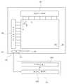
도 3은 본 발명의 실시예에 의한 액정표시장치의 구성을 개략적으로 도시한 블록도로써, 도 3을 참조하면, 제1 기판상에 다수개의 박막트랜지스터(T)가 매트릭스형태로 구비되고, 상기 박막트랜지스터(T)에 데이터신호의 입력을 제어하는 게이트드라이버(140) 및, 데이터신호를 출력하는 데이터드라이버(160)와, 주변 휘도 및 조도를 감지하는 포토센서(150)와, 상기 포토센서(150)로부터 감지된 휘도 및 조도에 대한 신호를 변환하고, 이를 통해 제어신호를 생성하는 신호처리부(170)와, 상기 포토센서(150) 및 상기 신호처리부(170)의 사이에 구비되는 센서제어부(157)가 포함된 액정패널(100)과, 상기 액정패널(100)의 배면으로 광을 조사하기 위한 백라이트 유닛(180)으로 구성되며, 이 백라이트 유닛(180)은 상기 액정패널(100)의 배면에 구성되어 데이터신호의 시각적 표시를 수행하는 백라이트램프(180a)와, 상기 백라이트램프(180a)를 제어하는 백라이트 제어부(180b)가 포함된다.3 is a block diagram schematically illustrating a configuration of a liquid crystal display according to an exemplary embodiment of the present invention. Referring to FIG. 3, a plurality of thin film transistors T are provided on a first substrate in a matrix form. A
도시되지는 않았지만 상기 백라이트램프(180a)는 하나 이상의 형광램프 또는 복수개의 LED(Light emitting diode)일 수 있다.Although not shown, the
또한, 도시하지는 않았지만, 상기 구성은 각각 구동에 요구되는 적합한 전원을 공급하는 전원공급부(미도시)에 의해 구동 전원을 공급받으며, 상기 전원공급부(미도시)는 통상 인쇄회로기판(PCB) 상에 집적되어 구성된다.In addition, although not shown, the configuration is supplied with driving power by a power supply unit (not shown) for supplying a suitable power required for driving, respectively, and the power supply unit (not shown) is usually on a printed circuit board (PCB). It is integrated.
보다 상세하게는, 액정패널(100)의 표시영역(120)에는 다수개의 게이트라인(GL) 및 데이터라인(DL)이 매트릭스 형태로 교차하여 형성되며, 상기 게이트라인(GL)과 데이터라인(DL)이 교차되는 지점에는 박막트랜지스터(T)가 구비된다.In more detail, a plurality of gate lines GL and data lines DL are formed in the
또한, 상기 액정패널(100)의 비표시영역(130)에는 외부로부터 주사신호 및 데이터신호를 입력받아 상기 게이트라인(GL)과 데이터라인(DL)을 통해 상기 표시영 역(120)의 박막트랜지스터(T)를 제어하는 게이트드라이버(140) 및 데이터드라이버(160)가 실장된다.In addition, the
상기 액정패널(100)의 하측단에는 적어도 하나의 포토센서(150)가 구비된다. 이 포토센서(150)는 표시영역(120)과 비표시영역(130)의 경계선에 구비되며, 표시영역(120)내에 구비될 수도 있고, 비표시영역(130)에 구비될 수도 있다. 다시 말하면, 상기 포토센서(150)는 액정패널내에 구비되어, 액정표시장치가 적용된 전자기기에서 포토센서를 구비하기 위한 별도의 영역을 필요로 하지 않는다.At least one
여기서, 상기 포토센서(150)는 포토다이오드 혹은 포토트랜지스터로 구성될 수 있다.Here, the
또한, 비표시영역(130)의 하측단에는 상기 포토센서(150)와 연결되어 입력되는 신호를 변환하고, 이를 통해 제어신호를 생성하는 신호처리부(170)가 구비되고, 이 신호처리부(170)는 액정패널(100)의 배면으로 구비되는 백라이트 유닛(180)의 백라이트 제어부(180b)와 연결된다.In addition, a lower portion of the
여기서, 포토센서(150)는 포토다이오드 혹은 포토트랜지스터로 구성될 수 있다. 상기 포토센서(150) 및 상기 신호처리부(170)는 박막트랜지스터(T)와 동일한 공정에서 형성되며, 상기 포토센서(150)는 실제로 광에 반응하는 부분은 아모퍼스등으로 형성되고, 나머지 부분은 폴리 실시콘으로 형성된다. Here, the
이하, 도 3을 참조하여 본 발명의 실시예에 액정표시장치의 동작을 설명하면 다음과 같다.Hereinafter, the operation of the liquid crystal display device according to the exemplary embodiment of the present invention will be described with reference to FIG. 3.
액정패널(100)은 다수개의 게이트라인(GL) 및 데이터라인(DL)이 매트릭스 형 태로 교차하여 배치되며, 교차 지점에 박막트랜지스터(T)를 스위칭 소자로써 구비하고 후술하는 드라이버(140, 160)와, 포토센서(150)와, 신호처리부(170)를 포함한다. 이 박막트랜지스터(T)의 스위칭 동작으로 액정물질의 광 투과율을 변화시켜 영상을 표시한다.The
게이트드라이버(140)는 타이밍 컨트롤러(미도시)로부터 출력되는 제어신호에 대응하여, 게이트출력신호를 생성하고, 이를 게이트라인(GL)을 통해 순차적으로 상기 박막트랜지스터(T)로 출력한다.The
데이터드라이버(160)는 타이밍 컨트롤러(미도시)로부터 제어신호 및 데이터신호에 대응하여, 디지털형태의 데이터신호를 아날로그 형태의 영상신호로 변환하고, 이를 데이터라인(DL)을 통해 상기 박막트랜지스터(T)로 출력한다.The
포토센서(150)는 외광의 휘도 및 조도를 감지하고, 이에 상응하는 전류신호를 센서제어부(157)로 출력한다.The photosensor 150 senses the brightness and illuminance of the external light and outputs a current signal corresponding thereto to the
센서제어부(157)는 상기 포토센서(150)로부터 입력되는 전류신호를 설정자가 미리 설정해놓은 전압신호로 변환하여 신호처리부(170)에 공급한다.The
신호처리부(170)는 상기 포토센서(150)로부터 전압신호를 입력받아 상기 아날로그 형태의 전압신호를 디지털 형태의 전압신호로 변환한다. 또한 이러한 과정을 거쳐 변환된 신호를 백라이트 제어부(180b)로 공급한다.The
백라이트유닛(180)은 하나이상의 램프로 구성되는 백라이트램프(180a)로 상기 액정패널(100)에 광을 조사한다. 이 백라이트램프(180a)의 휘도는 백라이트 제어부(180b)를 통해 제어된다.The
이에 따라, 상기 게이트드라이버(140) 및 데이터드라이버(160)로부터 출력되는 게이트구동신호 및 영상신호를 통해 구비되어 있는 박막트랜지스터(T)를 턴-온/오프하여, 액정셀의 광 투과율을 변화시키고, 백라이트 유닛으로 광을 조사하여 영상을 표시한다.Accordingly, the thin film transistor T provided through the gate driving signal and the image signal output from the
이때, 상기 백라이트 제어부(180b)는 상기 신호처리부(170, 157)에서 공급되는 외부 휘도가 기준 휘도에 비해 밝을 경우, 상기 백라이트램프(180a)에 공급되는 전압을 크게 인가하고, 이를 통해 상기 백라이트램프(180a)에서 발생하는 광의 휘도를 크게 발생하여 외부 광에 따른 휘도 및 명암비가 떨어지는 것을 방지한다.In this case, when the external luminance supplied from the
또한, 외부 휘도가 기준 휘도에 비해 어두울 경우 상기 백라이트램프(180a)에 공급되는 전압을 작게 인가하고, 이를 통해 상기 백라이트램프(180a)에서 발생하는 광의 휘도를 작게 발생하여 불필요한 전력소모을 방지할 수 있다.In addition, when the external luminance is darker than the reference luminance, the voltage supplied to the
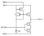
도 4a는 도 3의 센서제어부를 보다 구체적으로 도시한 회로도로서, 여기서, 포토다이오드(D1)는 도 3의 포토센서(도 3의 150)로서, 일 예를 든 것이다. 또한, 제1 내지 제3 트랜지스터는 P-MOS로 구현되며, 제4, 제5 트랜지스터(T1, T4, T5)는 N-MOS로 구현된다.FIG. 4A is a circuit diagram illustrating the sensor controller of FIG. 3 in more detail. Here, the photodiode D1 is an example of the
구조를 살펴보면, 제1 트랜지스터(T1)는 인에에블신호(EN)를 입력받아, 이 인에이블신호(EN)를 N1노드(N1)로 인가하고, 포토다이오드(D1)는 입사되는 광의 크기에 따라, 상기 N1노드의 전류의 세기를 조절하고, 이에 따라, 제2 및 제3 트랜지스터(T2 ,T3)를 턴-온/오프 시켜, 상기 인에이블신호(EN)를 출력단(Vout)을 통해 출력하며, 제4 및 제5 트랜지스터(T4, T5)는 가변저항 역할을 하는 구조이다.Referring to the structure, the first transistor T1 receives the enable signal EN, applies the enable signal EN to the N1 node N1, and the photodiode D1 receives the magnitude of the incident light. As a result, the intensity of the current of the N1 node is adjusted, and accordingly, the second and third transistors T2 and T3 are turned on / off to output the enable signal EN through the output terminal Vout. The fourth and fifth transistors T4 and T5 serve as variable resistors.
이하, 도 4a을 참조하여 본 발명의 제1 실시예에 의한 액정표시장치 구동회로의 구조를 설명하면 다음과 같다.Hereinafter, the structure of the liquid crystal display driving circuit according to the first embodiment of the present invention will be described with reference to FIG. 4A.
제1 트랜지스터(T1)는 게이트단 및 소스단이 인에에블신호(EN) 입력단과 연결되고, 드레인단이 N1노드(N1)와 연결된다.In the first transistor T1, a gate terminal and a source terminal are connected to an enable signal EN input terminal, and a drain terminal thereof is connected to an N1 node N1.
제2 트랜지스터(T2)는 게이트단 및 드레인단이 상기 N1노드(N1)와 연결되고, 소스단이 상기 인에에블신호(EN) 입력단과 연결된다.In the second transistor T2, a gate terminal and a drain terminal are connected to the N1 node N1, and a source terminal is connected to the enable signal EN input terminal.
제3 트랜지스터(T3)는 게이트단이 상기 N1노드(N1)와 연결되고, 소스단이 상기 인에이블신호(EN) 입력단과 연결되며, 드레인단이 출력단(Vout)과 연결된다.In the third transistor T3, a gate terminal is connected to the N1 node N1, a source terminal is connected to the enable signal EN input terminal, and a drain terminal is connected to the output terminal Vout.
제4 트랜지스터(T4)는 게이트단이 가변저항신호(VBIAS)입력단과 연결되고, 드레인단은 상기 출력단(Vout)과 연결된다.In the fourth transistor T4, a gate terminal thereof is connected to a variable resistance signal VBIAS input terminal, and a drain terminal thereof is connected to the output terminal Vout.
제5 트랜지스터(T5)는 게이트단이 가변저항신호(VBIAS)입력단과 연결되고, 소스단은 접지전압(VSS)단과 연결되며, 드레인단은 상기 제4 트랜지스터(T4)와 연결된다.In the fifth transistor T5, a gate terminal thereof is connected to a variable resistance signal VBIAS input terminal, a source terminal thereof is connected to a ground voltage VSS terminal, and a drain terminal thereof is connected to the fourth transistor T4.
포토 다이오드(D1)는 애노드가 접지전압단(VSS)와 연결되고, 캐소드가 상기 N1노드(N1)와 연결된다.The photodiode D1 has an anode connected to the ground voltage terminal VSS and a cathode connected to the N1 node N1.
이하, 도 4a를 참조하여 본 발명의 제1 실시예에 의한 액정표시장치 구동회로의 동작을 설명하면 다음과 같다.Hereinafter, an operation of the liquid crystal display driving circuit according to the first embodiment of the present invention will be described with reference to FIG. 4A.
먼저, 센서제어부(157)에 하이레벨의 인에이블신호(EN)가 인가되고, 포토다이오드(D1)에 광이 입사되어 전류가 흐르면 전류는 애노드에서 캐소드방향으로 흐르게 된다. 이에 따라, 상기 포토다이오드(D1)의 캐소드에 연결되어 있는 N1노 드(N1)에 흐르는 전류값은 낮아지게 된다. 이때, 전류가 흐르게 되면, 전압이 인가되는 것으로 N1노드(N1)의 전압이 제2 트랜지스터(T2)와 제3 트랜지스터(T3)의 게이트에 인가되고, 상기 제2 트랜지스터(T2)와 제3 트랜지스터(T3)는 N1노드(N1)전압이 문턱전압(Vth)이하가 되면, 턴-온되어 상기 N1노드(N1)에 흐르는 전류에 대응되는 전압이 트랜지스터(T3)의 드레인단에 연결되어 있는 출력단(Vout)을 통해 출력되게 된다.First, when a high level enable signal EN is applied to the
이때, 상기 출력단(Vout)에 인가되는 전압은 최종적으로 가변저항신호(VBIAS)의 인가에 따라 결정된다. 즉, 제4 트랜지스터(T4) 및 제5 트랜지스터(T5)의 턴-온/오프에 따라 상기 출력단(Vout)을 통해 흐르는 전류의 일부가 접지전압단으로 흐르기 때문에, 가변저항신호(VBIAS)로 출력단(Vout)에 인가되는 전압의 크기를 조절할 수 있다.At this time, the voltage applied to the output terminal Vout is finally determined according to the application of the variable resistance signal VBIAS. That is, a part of the current flowing through the output terminal Vout flows to the ground voltage terminal according to the turn-on / off of the fourth transistor T4 and the fifth transistor T5, and thus the output terminal is converted into the variable resistance signal VBIAS. The magnitude of the voltage applied to (Vout) can be adjusted.
그리고, 센서제어부(157)에 로우레벨의 인에이블신호(EN)가 인가되면, 상기 제1 트랜지스터(T1)는 턴-온되어, 상기 N1노드(N1)에 흐르는 전류가 인에이블신호(EN)단으로 방전된다. 또한, 상기 제2 트랜지스터(T2)는 게이트단과 드레인단이 연결되어 있으므로, 다이오드 동작을 하며 상기 포토다이오드(D1)와 마주보는 형태가 되기 때문에, 상기 N1노드(N1)의 전류의 크기는 상기 포토다이오드(D1)를 통해 흐르는 전류의 크기에 영향을 받게 된다. 제3 트랜지스터(T3)는 상기 N1노드(N1)의 전압에 의해, 턴-온되어 출력단(Vout)에 걸리는 전압이 방전한다. 상기 제4 및 제5 트랜지스터(T4, T5)의 동작은 상술한 바와 동일하다.When the low level enable signal EN is applied to the
또한, 상기 제4 및 제5 트랜지스터(T4, T5)는 상술한 바와 같이, 가변저항소 자의 역할을 하므로, 상황에 따라 하나의 트랜지스터로만 형성될 수 있다.In addition, since the fourth and fifth transistors T4 and T5 play a role of the variable resistor element as described above, the fourth and fifth transistors T4 and T5 may be formed of only one transistor according to circumstances.
따라서, 포토센서의 감지결과에 따른 전류신호를 용이하게 제어가능하여, 포토센서의 신뢰성을 보다 확보할 수 있다.Therefore, it is possible to easily control the current signal according to the detection result of the photosensor, it is possible to ensure the reliability of the photosensor more.
도 4b는 도 3의 센서제어부를 보다 구체적으로 도시한 다른 형태의 회로도로서, 도 4a에서 제1 트랜지스터(T1)의 소스단이 N1노드(N1)가 아닌 전원전압(VDD)단과 연결되어 형태이며, 그 이외의 소자들 및 이 소자들의 연결형태는 도 4a 와 동일하고, 이하에서는 상기 도 4a에 나타낸 구동회로와의 차이점만을 설명하도록 한다.FIG. 4B is another circuit diagram illustrating the sensor controller of FIG. 3 in more detail. In FIG. 4A, the source terminal of the first transistor T1 is connected to the power supply voltage VDD instead of the N1 node N1. The other elements and the connection form of these elements are the same as in FIG. 4A, and only the differences from the driving circuit shown in FIG. 4A will be described below.
도 4b의 구동회로는 N1노드(N1)를 전원전압(VDD)레벨로 설정하기 위한 일 예로서, 하이레벨의 인에이블신호(EN)가 인가되는 경우, 도 4a의 구동회로와 동일한 동작을 수행하며, 로우레벨의 인에에블신호(EN)가 인가되는 경우, 제1 트랜지스터(T1)가 턴-온되어, 소스단에 연결되어 있는 전원전압(VDD)이 N1노드(N1)에 인가된다.The driving circuit of FIG. 4B is an example for setting the N1 node N1 to the power supply voltage VDD level. When the high level enable signal EN is applied, the driving circuit of FIG. 4B performs the same operation as that of the driving circuit of FIG. 4A. When the low level enable signal EN is applied, the first transistor T1 is turned on so that the power supply voltage VDD connected to the source terminal is applied to the N1 node N1. .
도 4c는 도 3의 센서제어부를 보다 구체적으로 도시한 또 다른 형태의 회로도로서, 도 4a 및 도 4b의 제1 트랜지스터(T1)가 P-MOS가 아닌 N-MOS로 구비되며, 상기 제1 트랜지스터(T1)의 게이트단이 인에이블신호(EN)단과 인버터(I1)를 사이에 두고 연결되고, 소스단이 전원전압(VDD)단에 연결되고, 드레인단은 N1노드(N1)에 연결되는 형태이며, 그 이외의 소자들 및 이 소자들의 연결형태는 도 4a 및 도 4b와 동일하고, 이하에서는 상기 도 4a 및 도 4b에 나타낸 구동회로와의 차이점만을 설명하도록 한다.FIG. 4C is another circuit diagram illustrating the sensor controller of FIG. 3 in more detail. The first transistor T1 of FIGS. 4A and 4B is provided as an N-MOS instead of a P-MOS. The gate terminal of T1 is connected with the enable signal EN terminal and the inverter I1 interposed therebetween, the source terminal is connected to the power supply voltage VDD terminal, and the drain terminal is connected to the N1 node N1. The other elements and the connection form of the elements are the same as those of FIGS. 4A and 4B, and only the differences from the driving circuits shown in FIGS. 4A and 4B will be described below.
도 4c의 구동회로는 N1노드(N1)를 접지전압(VSS)레벨로 설정하기 위한 일 예로서, 하이레벨의 인에이블신호(EN)가 인가되는 경우, 도 4a 및 도 4b의 구동회로와 동일한 동작을 수행하며, 로우레벨의 인에에블신호(EN)가 인가되는 경우, 제1 트랜지스터(T1)가 턴-온되어, 소스단에 연결되어 있는 접지전압(VSS)이 N1노드(N1)에 인가된다.The driving circuit of FIG. 4C is an example for setting the N1 node N1 to the ground voltage VSS level. When the high level enable signal EN is applied, the driving circuit of FIG. 4C is the same as the driving circuit of FIGS. 4A and 4B. When the low level enable signal EN is applied, the first transistor T1 is turned on so that the ground voltage VSS connected to the source terminal is N1 node N1. Is applied to.
상기에서는 본 발명의 바람직한 실시예를 참조하여 설명하였지만, 해당 기술분야의 숙련된 당업자는 하기의 특허청구범위에 기재된 본 발명의 기술적 사상 및 영역으로부터 벗어나지 않는 범위내에서 본 발명을 다양하게 수정 및 변경시킬 수 있음을 이해할 수 있을 것이다.It will be apparent to those skilled in the art that various modifications and variations can be made in the present invention without departing from the spirit or scope of the invention as defined in the appended claims. It can be understood that
따라서, 본 발명의 실시에에 의한 본 발명은 액정표시장치 및 이의 구동회로로는 액정표시장치의 백라이트 유닛을 외부 휘도의 크기에 따라 제어하여 야외시인성 증가 및 소비전력을 절감하는 효과가 있다.Therefore, according to the present invention according to the embodiment of the present invention, the liquid crystal display and its driving circuit control the backlight unit of the liquid crystal display according to the size of the external luminance, thereby increasing the outdoor visibility and reducing the power consumption.
또한, 외부 휘도의 크기를 감지하기 위한 포토센서를 효과적으로 제어하는 센서제어부를 통해, 상기 포토센서 동작의 신뢰성을 확보할 수 있다.In addition, through the sensor controller for effectively controlling the photosensor for sensing the magnitude of the external luminance, it is possible to ensure the reliability of the photosensor operation.
또한, 상기 센서제어부를 다양한 설정값을 갖도록 구성가능하다.In addition, the sensor controller may be configured to have various setting values.
Claims (8)
Translated fromKoreanPriority Applications (4)
| Application Number | Priority Date | Filing Date | Title |
|---|---|---|---|
| KR1020060060919AKR101229019B1 (en) | 2006-06-30 | 2006-06-30 | Liquid crystal display device and driving circuit of the same |
| CNB200610165630XACN100538809C (en) | 2006-06-30 | 2006-12-08 | Liquid crystal indicator and driving method thereof |
| US11/638,514US7733336B2 (en) | 2006-06-30 | 2006-12-14 | Liquid crystal display device and method of driving the same |
| TW095149346ATWI350508B (en) | 2006-06-30 | 2006-12-27 | Liquid crystal display device and method of driving the same |
Applications Claiming Priority (1)
| Application Number | Priority Date | Filing Date | Title |
|---|---|---|---|
| KR1020060060919AKR101229019B1 (en) | 2006-06-30 | 2006-06-30 | Liquid crystal display device and driving circuit of the same |
Publications (2)
| Publication Number | Publication Date |
|---|---|
| KR20080002233A KR20080002233A (en) | 2008-01-04 |
| KR101229019B1true KR101229019B1 (en) | 2013-02-15 |
Family
ID=38876093
Family Applications (1)
| Application Number | Title | Priority Date | Filing Date |
|---|---|---|---|
| KR1020060060919AActiveKR101229019B1 (en) | 2006-06-30 | 2006-06-30 | Liquid crystal display device and driving circuit of the same |
Country Status (4)
| Country | Link |
|---|---|
| US (1) | US7733336B2 (en) |
| KR (1) | KR101229019B1 (en) |
| CN (1) | CN100538809C (en) |
| TW (1) | TWI350508B (en) |
Families Citing this family (47)
| Publication number | Priority date | Publication date | Assignee | Title |
|---|---|---|---|---|
| GB0718706D0 (en) | 2007-09-25 | 2007-11-07 | Creative Physics Ltd | Method and apparatus for reducing laser speckle |
| KR100957948B1 (en)* | 2008-02-19 | 2010-05-13 | 삼성모바일디스플레이주식회사 | Optical sensor and flat panel display device using the same |
| CN101551979A (en) | 2008-04-03 | 2009-10-07 | 上海天马微电子有限公司 | Outdoor readable liquid crystal display device |
| JP5301294B2 (en)* | 2008-05-30 | 2013-09-25 | 株式会社ジャパンディスプレイウェスト | Display device |
| JP4797189B2 (en)* | 2009-02-09 | 2011-10-19 | 奇美電子股▲ふん▼有限公司 | Display device and electronic apparatus including the same |
| US9335604B2 (en) | 2013-12-11 | 2016-05-10 | Milan Momcilo Popovich | Holographic waveguide display |
| US11726332B2 (en) | 2009-04-27 | 2023-08-15 | Digilens Inc. | Diffractive projection apparatus |
| US20200057353A1 (en) | 2009-10-09 | 2020-02-20 | Digilens Inc. | Compact Edge Illuminated Diffractive Display |
| US8885112B2 (en) | 2009-10-27 | 2014-11-11 | Sbg Labs, Inc. | Compact holographic edge illuminated eyeglass display |
| TWI426330B (en)* | 2010-07-14 | 2014-02-11 | Chi Lin Optoelectronics Co Ltd | A backlight module and a display device including the backlight module |
| WO2012136970A1 (en) | 2011-04-07 | 2012-10-11 | Milan Momcilo Popovich | Laser despeckler based on angular diversity |
| US10670876B2 (en) | 2011-08-24 | 2020-06-02 | Digilens Inc. | Waveguide laser illuminator incorporating a despeckler |
| EP2995986B1 (en) | 2011-08-24 | 2017-04-12 | Rockwell Collins, Inc. | Data display |
| WO2016020630A2 (en) | 2014-08-08 | 2016-02-11 | Milan Momcilo Popovich | Waveguide laser illuminator incorporating a despeckler |
| WO2013034879A1 (en) | 2011-09-07 | 2013-03-14 | Milan Momcilo Popovich | Method and apparatus for switching electro optical arrays |
| US20150010265A1 (en) | 2012-01-06 | 2015-01-08 | Milan, Momcilo POPOVICH | Contact image sensor using switchable bragg gratings |
| KR101491613B1 (en)* | 2012-02-28 | 2015-02-16 | 주식회사 케이티 | Device and method for outputing audible sound, and measuring device for satellite signal |
| EP2862026A1 (en) | 2012-06-18 | 2015-04-22 | Milan Momcilo Popovich | Apparatus for copying a hologram |
| US9933684B2 (en) | 2012-11-16 | 2018-04-03 | Rockwell Collins, Inc. | Transparent waveguide display providing upper and lower fields of view having a specific light output aperture configuration |
| WO2015015138A1 (en) | 2013-07-31 | 2015-02-05 | Milan Momcilo Popovich | Method and apparatus for contact image sensing |
| US10359736B2 (en) | 2014-08-08 | 2019-07-23 | Digilens Inc. | Method for holographic mastering and replication |
| WO2016042283A1 (en) | 2014-09-19 | 2016-03-24 | Milan Momcilo Popovich | Method and apparatus for generating input images for holographic waveguide displays |
| WO2016113534A1 (en) | 2015-01-12 | 2016-07-21 | Milan Momcilo Popovich | Environmentally isolated waveguide display |
| US9632226B2 (en) | 2015-02-12 | 2017-04-25 | Digilens Inc. | Waveguide grating device |
| US10490141B1 (en)* | 2015-09-28 | 2019-11-26 | Amazon Technologies, Inc. | Reset pulse control to manage flicker of an electrowetting display device |
| CN113759555B (en) | 2015-10-05 | 2024-09-20 | 迪吉伦斯公司 | Waveguide Display |
| CN108780224B (en) | 2016-03-24 | 2021-08-03 | 迪吉伦斯公司 | Method and apparatus for providing a polarization selective holographic waveguide device |
| US10890707B2 (en) | 2016-04-11 | 2021-01-12 | Digilens Inc. | Holographic waveguide apparatus for structured light projection |
| WO2018102834A2 (en) | 2016-12-02 | 2018-06-07 | Digilens, Inc. | Waveguide device with uniform output illumination |
| US10545346B2 (en) | 2017-01-05 | 2020-01-28 | Digilens Inc. | Wearable heads up displays |
| WO2019079350A2 (en) | 2017-10-16 | 2019-04-25 | Digilens, Inc. | Systems and methods for multiplying the image resolution of a pixelated display |
| US10732569B2 (en) | 2018-01-08 | 2020-08-04 | Digilens Inc. | Systems and methods for high-throughput recording of holographic gratings in waveguide cells |
| EP3710894B1 (en) | 2018-01-08 | 2025-07-30 | Digilens Inc. | Methods for fabricating optical waveguides |
| EP3710876A4 (en) | 2018-01-08 | 2022-02-09 | DigiLens Inc. | SYSTEMS AND METHODS OF FABRICATING WAVEGUIDE CELLS |
| WO2019136476A1 (en) | 2018-01-08 | 2019-07-11 | Digilens, Inc. | Waveguide architectures and related methods of manufacturing |
| WO2020023779A1 (en) | 2018-07-25 | 2020-01-30 | Digilens Inc. | Systems and methods for fabricating a multilayer optical structure |
| US20200225471A1 (en) | 2019-01-14 | 2020-07-16 | Digilens Inc. | Holographic Waveguide Display with Light Control Layer |
| US20200247017A1 (en) | 2019-02-05 | 2020-08-06 | Digilens Inc. | Methods for Compensating for Optical Surface Nonuniformity |
| US20220283377A1 (en) | 2019-02-15 | 2022-09-08 | Digilens Inc. | Wide Angle Waveguide Display |
| KR102866596B1 (en) | 2019-02-15 | 2025-09-29 | 디지렌즈 인코포레이티드. | Method and device for providing a holographic waveguide display using an integral grating |
| WO2020186113A1 (en) | 2019-03-12 | 2020-09-17 | Digilens Inc. | Holographic waveguide backlight and related methods of manufacturing |
| EP3980825A4 (en) | 2019-06-07 | 2023-05-03 | Digilens Inc. | WAVEGUIDES WITH TRANSMITTING AND REFLECTING GRIDS AND RELATED MANUFACTURING PROCESSES |
| EP4004646A4 (en) | 2019-07-29 | 2023-09-06 | Digilens Inc. | METHODS AND APPARATUS FOR MULTIPLYING THE IMAGE RESOLUTION AND FIELD OF VIEW OF A PIXELATED DISPLAY SCREEN |
| KR102775783B1 (en) | 2019-08-29 | 2025-02-28 | 디지렌즈 인코포레이티드. | Vacuum grid and method for manufacturing the same |
| CN111223458B (en)* | 2020-01-06 | 2022-02-15 | 昆山龙腾光电股份有限公司 | Display module and electronic equipment |
| WO2022150841A1 (en) | 2021-01-07 | 2022-07-14 | Digilens Inc. | Grating structures for color waveguides |
| US12158612B2 (en) | 2021-03-05 | 2024-12-03 | Digilens Inc. | Evacuated periodic structures and methods of manufacturing |
Citations (2)
| Publication number | Priority date | Publication date | Assignee | Title |
|---|---|---|---|---|
| JP2006091051A (en)* | 2004-09-21 | 2006-04-06 | Seiko Epson Corp | Display device and electronic apparatus equipped with the same |
| US20060077169A1 (en) | 2004-10-12 | 2006-04-13 | Seiko Epson Corporation | Photo detection circuit, method of controlling the same, electro-optical panel, electro-optical device, and electronic apparatus |
Family Cites Families (12)
| Publication number | Priority date | Publication date | Assignee | Title |
|---|---|---|---|---|
| US6087703A (en)* | 1994-06-07 | 2000-07-11 | Mitsubishi Denki Kabushiki Kaisha | Photodetector and photodetection circuit |
| TW379499B (en)* | 1998-05-14 | 2000-01-11 | Ind Tech Res Inst | Active pixel sensing cell |
| US6043478A (en)* | 1998-06-25 | 2000-03-28 | Industrial Technology Research Institute | Active pixel sensor with shared readout structure |
| WO2002047061A1 (en)* | 2000-12-06 | 2002-06-13 | Sony Corporation | Timing generating circuit for display and display having the same |
| FR2820882B1 (en)* | 2001-02-12 | 2003-06-13 | St Microelectronics Sa | THREE TRANSISTOR PHOTODETECTOR |
| FR2824665B1 (en)* | 2001-05-09 | 2004-07-23 | St Microelectronics Sa | CMOS TYPE PHOTODETECTOR |
| JP2004281922A (en) | 2003-03-18 | 2004-10-07 | Seiko Epson Corp | Light emitting device current control device |
| US6975008B2 (en)* | 2003-10-27 | 2005-12-13 | Eastman Kodak Company | Circuit for detecting ambient light on a display |
| JP3691050B2 (en)* | 2003-10-30 | 2005-08-31 | 総吉 廣津 | Semiconductor image sensor |
| WO2005057275A1 (en)* | 2003-12-08 | 2005-06-23 | Sony Corporation | Liquid crystal display and backlight adjusting method |
| US20060284824A1 (en)* | 2005-06-20 | 2006-12-21 | Yu-Kuang Yeh | Luminance auto-adjustment for displays |
| KR101330817B1 (en)* | 2006-06-30 | 2013-11-15 | 엘지디스플레이 주식회사 | Liquid crystal display device and driving thereof |
- 2006
- 2006-06-30KRKR1020060060919Apatent/KR101229019B1/enactiveActive
- 2006-12-08CNCNB200610165630XApatent/CN100538809C/ennot_activeExpired - Fee Related
- 2006-12-14USUS11/638,514patent/US7733336B2/ennot_activeExpired - Fee Related
- 2006-12-27TWTW095149346Apatent/TWI350508B/ennot_activeIP Right Cessation
Patent Citations (2)
| Publication number | Priority date | Publication date | Assignee | Title |
|---|---|---|---|---|
| JP2006091051A (en)* | 2004-09-21 | 2006-04-06 | Seiko Epson Corp | Display device and electronic apparatus equipped with the same |
| US20060077169A1 (en) | 2004-10-12 | 2006-04-13 | Seiko Epson Corporation | Photo detection circuit, method of controlling the same, electro-optical panel, electro-optical device, and electronic apparatus |
Also Published As
| Publication number | Publication date |
|---|---|
| CN101097695A (en) | 2008-01-02 |
| US7733336B2 (en) | 2010-06-08 |
| TW200802267A (en) | 2008-01-01 |
| KR20080002233A (en) | 2008-01-04 |
| CN100538809C (en) | 2009-09-09 |
| US20080001909A1 (en) | 2008-01-03 |
| TWI350508B (en) | 2011-10-11 |
Similar Documents
| Publication | Publication Date | Title |
|---|---|---|
| KR101229019B1 (en) | Liquid crystal display device and driving circuit of the same | |
| KR101330817B1 (en) | Liquid crystal display device and driving thereof | |
| US9324276B2 (en) | Liquid crystal display device and method for automatically controlling brightness | |
| US10891895B2 (en) | Light emitting device, display device, and LED display device | |
| KR100997977B1 (en) | Optical sensor and display device using same | |
| US6885356B2 (en) | Active-matrix type display device | |
| TW397965B (en) | Pixel circuits, display devices and electronic instruments with current-driven light-emitting elements | |
| CN103383835B (en) | A pixel circuit, display panel and display device | |
| US20060082523A1 (en) | Active organic electroluminescence display panel module and driving module thereof | |
| KR101457683B1 (en) | Liquid crystal display | |
| US7924262B2 (en) | Light source driving apparatus, display device having the same and method of driving a light source | |
| EP4207158A1 (en) | Display apparatus | |
| KR101325977B1 (en) | Photo sensor build-in LCD | |
| KR20170059541A (en) | Backlight unit and display apparatus including the same | |
| US20170372657A1 (en) | Electro-optical device, driving method for electro-optical device, and electronic apparatus | |
| US20100026673A1 (en) | Method and control board for eliminating power-off residual images in display and display using the same | |
| KR20060017312A (en) | Display device having an inspection circuit | |
| KR102412006B1 (en) | Organic light emitting display panel and organic light emitting display device comprising the same | |
| KR101712204B1 (en) | Display device and fabricating method thereof | |
| EP4513474A1 (en) | Display device and control method thereof | |
| KR20050067259A (en) | Organic electroluminescence diode and driving method of the same | |
| KR101675841B1 (en) | Photo Sensor of Display Device and Method of Manufacturing the Same | |
| KR101322151B1 (en) | Organic Light Emitting Display and method for driving the same | |
| KR101356994B1 (en) | Light emitting diode driving device, light emitting device and display device | |
| KR100752848B1 (en) | Inverter drive control method of LCD |
Legal Events
| Date | Code | Title | Description |
|---|---|---|---|
| PA0109 | Patent application | Patent event code:PA01091R01D Comment text:Patent Application Patent event date:20060630 | |
| PG1501 | Laying open of application | ||
| A201 | Request for examination | ||
| PA0201 | Request for examination | Patent event code:PA02012R01D Patent event date:20110629 Comment text:Request for Examination of Application Patent event code:PA02011R01I Patent event date:20060630 Comment text:Patent Application | |
| E902 | Notification of reason for refusal | ||
| PE0902 | Notice of grounds for rejection | Comment text:Notification of reason for refusal Patent event date:20120813 Patent event code:PE09021S01D | |
| E701 | Decision to grant or registration of patent right | ||
| PE0701 | Decision of registration | Patent event code:PE07011S01D Comment text:Decision to Grant Registration Patent event date:20130125 | |
| GRNT | Written decision to grant | ||
| PR0701 | Registration of establishment | Comment text:Registration of Establishment Patent event date:20130128 Patent event code:PR07011E01D | |
| PR1002 | Payment of registration fee | Payment date:20130129 End annual number:3 Start annual number:1 | |
| PG1601 | Publication of registration | ||
| FPAY | Annual fee payment | Payment date:20151228 Year of fee payment:4 | |
| PR1001 | Payment of annual fee | Payment date:20151228 Start annual number:4 End annual number:4 | |
| FPAY | Annual fee payment | Payment date:20161214 Year of fee payment:5 | |
| PR1001 | Payment of annual fee | Payment date:20161214 Start annual number:5 End annual number:5 | |
| FPAY | Annual fee payment | Payment date:20171218 Year of fee payment:6 | |
| PR1001 | Payment of annual fee | Payment date:20171218 Start annual number:6 End annual number:6 | |
| FPAY | Annual fee payment | Payment date:20181226 Year of fee payment:7 | |
| PR1001 | Payment of annual fee | Payment date:20181226 Start annual number:7 End annual number:7 | |
| FPAY | Annual fee payment | Payment date:20191212 Year of fee payment:8 | |
| PR1001 | Payment of annual fee | Payment date:20191212 Start annual number:8 End annual number:8 | |
| PR1001 | Payment of annual fee | Payment date:20241216 Start annual number:13 End annual number:13 |