KR101228649B1 - Manufacturing method of multi-component metal oxides thin film having superlattice structure in thermoelectric module - Google Patents
Manufacturing method of multi-component metal oxides thin film having superlattice structure in thermoelectric moduleDownload PDFInfo
- Publication number
- KR101228649B1 KR101228649B1KR1020110059721AKR20110059721AKR101228649B1KR 101228649 B1KR101228649 B1KR 101228649B1KR 1020110059721 AKR1020110059721 AKR 1020110059721AKR 20110059721 AKR20110059721 AKR 20110059721AKR 101228649 B1KR101228649 B1KR 101228649B1
- Authority
- KR
- South Korea
- Prior art keywords
- thin film
- superlattice structure
- metal oxide
- substrate
- oxide thin
- Prior art date
- Legal status (The legal status is an assumption and is not a legal conclusion. Google has not performed a legal analysis and makes no representation as to the accuracy of the status listed.)
- Expired - Fee Related
Links
Images


Classifications
- H—ELECTRICITY
- H10—SEMICONDUCTOR DEVICES; ELECTRIC SOLID-STATE DEVICES NOT OTHERWISE PROVIDED FOR
- H10N—ELECTRIC SOLID-STATE DEVICES NOT OTHERWISE PROVIDED FOR
- H10N10/00—Thermoelectric devices comprising a junction of dissimilar materials, i.e. devices exhibiting Seebeck or Peltier effects
- H10N10/80—Constructional details
- H10N10/85—Thermoelectric active materials
- H10N10/851—Thermoelectric active materials comprising inorganic compositions
- H10N10/855—Thermoelectric active materials comprising inorganic compositions comprising compounds containing boron, carbon, oxygen or nitrogen
- H—ELECTRICITY
- H10—SEMICONDUCTOR DEVICES; ELECTRIC SOLID-STATE DEVICES NOT OTHERWISE PROVIDED FOR
- H10N—ELECTRIC SOLID-STATE DEVICES NOT OTHERWISE PROVIDED FOR
- H10N10/00—Thermoelectric devices comprising a junction of dissimilar materials, i.e. devices exhibiting Seebeck or Peltier effects
- H10N10/01—Manufacture or treatment
- H—ELECTRICITY
- H10—SEMICONDUCTOR DEVICES; ELECTRIC SOLID-STATE DEVICES NOT OTHERWISE PROVIDED FOR
- H10N—ELECTRIC SOLID-STATE DEVICES NOT OTHERWISE PROVIDED FOR
- H10N10/00—Thermoelectric devices comprising a junction of dissimilar materials, i.e. devices exhibiting Seebeck or Peltier effects
- H10N10/80—Constructional details
- H10N10/85—Thermoelectric active materials
- H10N10/851—Thermoelectric active materials comprising inorganic compositions
- H10N10/854—Thermoelectric active materials comprising inorganic compositions comprising only metals
Landscapes
- Chemical & Material Sciences (AREA)
- Inorganic Chemistry (AREA)
- Engineering & Computer Science (AREA)
- Manufacturing & Machinery (AREA)
- Crystals, And After-Treatments Of Crystals (AREA)
- Physical Deposition Of Substances That Are Components Of Semiconductor Devices (AREA)
Abstract
Translated fromKoreanDescription
Translated fromKorean본 발명은 열전소자에 사용되는 것으로서, 자발적 초격자구조를 갖는 다성분계 금속산화물 박막제조방법에 관한 것이다. 보다 구체적으로 스핀코팅법으로 박막을 형성시키는 것에 관한 것이다.The present invention relates to a method for manufacturing a multi-component metal oxide thin film having a spontaneous superlattice structure, which is used in a thermoelectric device. More specifically, the present invention relates to forming a thin film by spin coating.
본 출원인에 의한 한국특허출원 제10-2010-0029518호는 "초격자구조의 다성분계 산화물 박막제조방법"에 관하여 개시하고 있다. 상기 특허출원된 기술은 기판상에 버퍼를 형성한 후, 스퍼터링으로 박막을 형성한 다음, 박막을 열처리하여 초격자구조로 형성시키는 것을 기술적 특징으로 한다.Korean Patent Application No. 10-2010-0029518 by the present applicant discloses a method for manufacturing a multicomponent oxide thin film having a superlattice structure. The patented technology is characterized by forming a buffer on a substrate, then forming a thin film by sputtering, and then heat treating the thin film to form a superlattice structure.
그런데 상기 특허출원된 기술은 박막을 스퍼터링으로 형성시키므로, 고가의 장비가 필요하며, 타겟(target)을 이용하므로 다양한 종류의 금속원소를 자유롭게 합성하는 것이 곤란하다는 문제점이 제기되었다.However, since the patented technology forms a thin film by sputtering, expensive equipment is required, and since a target is used, it is difficult to freely synthesize various kinds of metal elements.
본 발명에 따른 열전소자의 자발적 초격자구조 다성분계 금속산화물 박막제조방법은 다음과 같은 해결과제를 가진다.The spontaneous superlattice structure multicomponent metal oxide thin film manufacturing method of the thermoelectric device according to the present invention has the following problems.
첫째, 박막을 형성하는 금속원소를 자유롭게 선택하고자 한다.First, the metal element forming the thin film is freely selected.
둘째, 진공챔버 등의 고가의 장비가 없어도, 박막형성을 가능하게 하고자 한다.Second, even without expensive equipment such as a vacuum chamber, it is intended to enable thin film formation.
셋째, 스핀코팅으로 박막을 형성시킬 때의 최적조건을 찾아내고자 한다.Third, we want to find out the optimal conditions for forming thin films by spin coating.
넷째, 열전소자에 사용되는 금속산화물 박막을 용이하게 형성시키고자 한다.Fourth, to easily form a metal oxide thin film used in the thermoelectric element.
본 발명의 해결과제는 이상에서 언급한 것들에 한정되지 않으며, 언급되지 아니한 다른 해결과제들은 아래의 기재로부터 당업자에게 명확하게 이해되어질 수 있을 것이다.The problem of the present invention is not limited to those mentioned above, and other problems not mentioned will be clearly understood by those skilled in the art from the following description.
본 발명은 열전소자용 자발적 초격자구조 금속산화물 박막제조방법에 관한 것으로서, 스핀코팅을 이용한 열전소자의 자발적 초격자구조 다성분계 금속산화물 박막제조방법에 대한 기술이다.The present invention relates to a method for manufacturing a spontaneous superlattice metal oxide thin film for thermoelectric devices, and to a method for manufacturing a spontaneous superlattice multicomponent metal oxide thin film for a thermoelectric device using spin coating.
본 발명은 기판 상에 스퍼터링을 통해 ZnO 버퍼층이 형성되는 S1 단계를 포함한다.The present invention includes a step S1 in which a ZnO buffer layer is formed through sputtering on a substrate.
본 발명은 버퍼층이 형성된 기판을 회전시키면서, 상기 회전되는 기판 상에 금속소스 함유 용액을 떨어뜨리는 스핀코팅(spin-coating)법으로 박막을 형성하는 S2 단계를 포함한다.The present invention includes a step S2 of forming a thin film by a spin-coating method of rotating a substrate on which a buffer layer is formed while dropping a solution containing a metal source on the rotated substrate.
본 발명은 S2 단계에서 형성된 박막이 건조되는 S3 단계를 포함한다.The present invention includes an S3 step of drying the thin film formed in the S2 step.
본 발명은 S3 단계를 거친 박막을 열처리하여 초격자구조를 가진 금속산화물 박막이 형성되는 S4 단계를 포함한다.The present invention includes an S4 step of forming a metal oxide thin film having a superlattice structure by heat-treating the thin film passing through the S3 step.
본 발명에 따른 S1 단계의 기판은 육방정계(Hexagonal) 구조 또는 능면체(Rhombohedral) 구조를 가지면서 버퍼층을 이루는 물질과의 격자상수 차이가 1Å 이하인 물질로 이루어지는 것이 바람직하다.The substrate of step S1 according to the present invention is preferably made of a material having a hexagonal structure or a rhombohedral structure and having a lattice constant difference of 1 Å or less from a material constituting the buffer layer.
본 발명에 따른 기판은 Si, SiO2, ITO, 사파이어, 글래스, GaN 및 YSG로 이루어진 군 중에서 선택되는 어느 하나의 물질로 이루어지는 것이 바람직하다.The substrate according to the present invention is preferably made of any one material selected from the group consisting of Si, SiO2 , ITO, sapphire, glass, GaN and YSG.
본 발명에 따른 S1 단계의 ZnO 버퍼층은 ZnO, In-ZnO 및 Ga-ZnO로 이루어진 군 중에서 선택되는 어느 하나의 물질로서 단결정 또는 다결정인 것이 바람직하다.The ZnO buffer layer of step S1 according to the present invention is any one material selected from the group consisting of ZnO, In-ZnO, and Ga-ZnO, preferably monocrystalline or polycrystalline.
본 발명에 따른 버퍼층의 두께는 100nm를 초과하지 않는 것이 바람직하다.It is preferable that the thickness of the buffer layer according to the present invention does not exceed 100 nm.
본 발명에 따른 S2 단계의 금속소스 함유 용액에 포함된 금속 원소는 In, Al, Ga, Zn 및 Sn으로 이루어진 군 중에서 선택되는 하나 이상의 원소인 것이 바람직하다.The metal element included in the metal source-containing solution of step S2 according to the present invention is preferably at least one element selected from the group consisting of In, Al, Ga, Zn and Sn.
본 발명에 따른 S2 단계에서 기판 회전속도는 3,000rpm ~ 6,000rpm인 것이 바람직하다.In the step S2 according to the present invention, the substrate rotation speed is preferably 3,000 rpm to 6,000 rpm.
본 발명에 따른 S3 단계에서의 건조온도는 200℃ ~ 300℃ 인 것이 바람직하다.Drying temperature in step S3 according to the present invention is preferably 200 ℃ ~ 300 ℃.
본 발명에 따른 S3 단계에서의 건조시간은 10분 ~ 30분인 것이 바람직하다.The drying time in step S3 according to the present invention is preferably 10 minutes to 30 minutes.
본 발명에 따른 박막은 S2 단계 및 S3 단계를 반복적으로 수행하여 복수 개의 층으로 이루어지는 것이 바람직하다.The thin film according to the present invention is preferably made of a plurality of layers by repeatedly performing the steps S2 and S3.
본 발명에 따른 S4 단계의 열처리시간은 3hr ~ 9hr인 것이 바람직하다.Heat treatment time of the step S4 according to the present invention is preferably 3hr ~ 9hr.
본 발명에 따른 S4 단계의 열처리온도는 상기 기판이 사파이어 기판인 경우, 800℃ ~ 1,000℃인 것이 바람직하다.Heat treatment temperature of step S4 according to the present invention is preferably 800 ℃ ~ 1,000 ℃ when the substrate is a sapphire substrate.
본 발명에 따른 열전소자의 자발적 초격자구조 다성분계 금속산화물 박막제조방법은 다음과 같은 효과를 가진다.The spontaneous superlattice structure multicomponent metal oxide thin film manufacturing method of the thermoelectric device according to the present invention has the following effects.
첫째, 열전소자의 금속산화물 박막 형성을 위해 용액공정법 중 스핀코팅법을 도입함으로써, 금속원소의 선택을 자유롭게 할 수 있는 효과가 있다.First, by introducing a spin coating method of the solution process to form a metal oxide thin film of the thermoelectric element, there is an effect that can freely select the metal element.
둘째, 박막형성을 위한 진공챔버 등이 불필요하므로, 챔버 크기제약이 작아 대면적의 박막형성에 유리한 효과가 있다.Second, since there is no need for a vacuum chamber for forming a thin film, a small chamber size constraint is advantageous in forming a thin film of a large area.
셋째, 박막형성을 위해 스퍼터링법이 아닌 스핀코팅법을 채택함에 따라, 타겟이 불필요하며, 보다 용이하게 박막형성을 할 수 있는 효과가 있다.Third, by adopting a spin coating method rather than a sputtering method for forming a thin film, a target is unnecessary and there is an effect of forming a thin film more easily.
넷째, 자발적으로 초격자구조를 보이는 In-Ga-Zn-Sn-Al를 성분원소로 하는 다성분계 금속산화물 박막을 용이하게 형성할 수 있다.Fourth, it is possible to easily form a multi-component metal oxide thin film having In-Ga-Zn-Sn-Al having a spontaneous superlattice structure as a component element.
본 발명의 효과는 이상에서 언급한 것들에 한정되지 않으며, 언급되지 아니한 다른 효과들은 아래의 기재로부터 당업자에게 명확하게 이해되어질 수 있을 것이다.The effects of the present invention are not limited to those mentioned above, and other effects that are not mentioned will be clearly understood by those skilled in the art from the following description.
도 1은 본 발명에 따른 금속산화물 박막의 제조방법을 나타내는 공정도이다.
도 2a 및 도 2b는 ZnO 버퍼층에 의해 기판과 박막 사이의 격자상수 불일치가 감소되는 것을 나타내는 개념도이다.
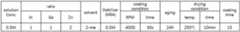
도 3은 본 발명에 따른 S2 단계에서, 스핀코팅 공정조건의 일 실시예를 나타낸다.
도 4는 본 발명에 따른 S3 단계에서, 스핀코팅법으로 증착된 InGaZnO 박막을 150℃에서 건조한 시편의 TEM 자료이다.
도 5는 본 발명에 따른 S3 단계에서, 스핀코팅법으로 증착된 InGaZnO 박막을 250℃에서 건조한 시편의 TEM 자료이다.
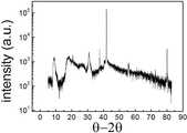
도 6은 본 발명에 따른 S4 단계에서, 사파이어 기판을 사용하고 ZnO 버퍼층이 형성된 실시예에서 열처리온도 1000℃, 열처리시간 9hr인 경우에 측정된 XRD 분석결과이다.
도 7은 본 발명에 따른 S4 단계에서, 사파이어 기판을 사용하고 ZnO 버퍼층이 형성된 실시예에서 열처리온도 900℃, 열처리시간 9hr인 경우에 측정된 XRD 분석결과이다.
도 8은 본 발명에 따른 스핀코팅법으로 성장한 박막이 열처리 후 성공적으로 초격자구조를 형성함을 나타내는 XRD 분석결과이다.
도 9는 온도(Temp) 대비 지벡계수(Seebeck coefficient)를 나타내는 데이터이다.
도 10은 사파이어기판 및 ZnO 버퍼층 하에서 열처리온도 900℃, 열처리시간 9hr으로 InGaZnO 박막 두께를 목표값보다 두껍게 한 실시예의 데이터를 나타낸다.
도 11은 사파이어기판 및 ZnO 버퍼층 하에서 열처리온도 900℃, 열처리시간 9hr으로 InGaZnO 박막 두께를 목표값보다 얇게 한 실시예의 데이터를 나타낸다.1 is a process chart showing a method of manufacturing a metal oxide thin film according to the present invention.
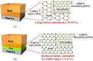
2A and 2B are conceptual views illustrating that the lattice constant mismatch between the substrate and the thin film is reduced by the ZnO buffer layer.
Figure 3 shows an embodiment of the spin coating process conditions in step S2 according to the present invention.
FIG. 4 is TEM data of a specimen dried at 150 ° C. with an InGaZnO thin film deposited by spin coating in step S3 according to the present invention.
FIG. 5 is TEM data of a specimen dried at 250 ° C. in an InGaZnO thin film deposited by spin coating in step S3 according to the present invention.
FIG. 6 is an XRD analysis result measured at a heat treatment temperature of 1000 ° C. and a heat treatment time of 9 hr in an example in which a sapphire substrate is used and a ZnO buffer layer is formed in step S4 according to the present invention.
FIG. 7 is an XRD analysis result measured at a heat treatment temperature of 900 ° C. and a heat treatment time of 9 hr in an example in which a sapphire substrate is used and a ZnO buffer layer is formed in step S4 according to the present invention.
8 is an XRD analysis showing that a thin film grown by spin coating according to the present invention successfully forms a superlattice structure after heat treatment.
FIG. 9 is data showing Seebeck coefficient vs. temperature Temp.
FIG. 10 shows data of an example in which an InGaZnO thin film was thicker than a target value at a heat treatment temperature of 900 ° C. and a heat treatment time of 9 hr under a sapphire substrate and a ZnO buffer layer.
FIG. 11 shows data of an example in which an InGaZnO thin film was thinner than a target value at a heat treatment temperature of 900 ° C. and a heat treatment time of 9 hr under a sapphire substrate and a ZnO buffer layer.
이하, 첨부된 도면들 및 후술 되어 있는 내용을 참조하여 본 발명의 바람직한 실시예들을 상세히 설명한다. 그러나, 본 발명은 여기서 설명되는 실시예들에 한정되지 않고 다른 형태로 구체화될 수도 있다. 오히려, 여기서 소개되는 실시예들은 개시된 내용이 철저하고 완전해질 수 있도록 그리고 당업자에게 본 발명의 기술적 사상이 충분히 전달될 수 있도록 하기 위해 제공되어 지는 것이다.Hereinafter, exemplary embodiments of the present invention will be described in detail with reference to the accompanying drawings and the contents described below. However, the present invention is not limited to the embodiments described herein and may be embodied in other forms. Rather, the embodiments introduced herein are provided to ensure that the disclosed contents are thorough and complete, and that the technical spirit of the present invention can be sufficiently delivered to those skilled in the art.
첨부된 도면들에 있어서, 층 및 영역들의 두께는 내용 전달의 명확성을 기하기 위하여 일부 과장되어 있음을 밝힌다. 본 명세서 전체에 걸쳐서 동일한 참조번호들은 동일한 구성요소들을 나타낸다.
In the accompanying drawings, it is apparent that the thicknesses of layers and regions are partially exaggerated for clarity of content transfer. Like numbers refer to like elements throughout.
이하 본 발명의 바람직한 실시예에 대하여 구체적으로 설명한다.Hereinafter, a preferred embodiment of the present invention will be described in detail.
도 1은 본 발명에 따른 금속산화물 박막의 제조방법을 나타내는 공정도이다. 본 발명은 열전소자용 자발적 초격자구조 금속산화물 박막제조방법에 관한 것으로서, 기판 상에 스퍼터링을 통해 ZnO 버퍼층이 형성되는 S1 단계; 상기 버퍼층이 형성된 기판을 회전시키면서, 회전되는 기판 상에 금속소스 함유 용액을 떨어뜨리는 스핀코팅(spin-coating)법으로 박막을 형성하는 S2 단계; S2 단계에서 형성된 박막이 건조되는 S3 단계; 및 S3 단계를 거친 박막을 열처리하여 초격자구조를 가진 금속산화물 박막이 형성되는 S4 단계를 포함한다.1 is a process chart showing a method of manufacturing a metal oxide thin film according to the present invention. The present invention relates to a method for manufacturing a spontaneous superlattice metal oxide thin film for thermoelectric devices, comprising: a step S1 of forming a ZnO buffer layer through sputtering on a substrate; S2 step of forming a thin film by spin-coating (dropping) the metal source containing solution on the rotated substrate while rotating the substrate on which the buffer layer is formed; S3 step of drying the thin film formed in the step S2; And an S4 step of forming a metal oxide thin film having a superlattice structure by heat-treating the thin film having passed through the S3 step.
본 발명에 따른 S1단계에 있어서, 기판 상에 스퍼터링(sputtering)을 통해 버퍼층이 형성된다.In step S1 according to the present invention, a buffer layer is formed on the substrate through sputtering.
본 발명에 따른 기판은 육방정계(Hexagonal) 구조 또는 능면체(Rhombohedral) 구조를 가지면서 버퍼층을 이루는 ZnO 물질과의 격자상수 차이가 1Å 이하인 물질로 이루어질 수 있다. 육방정계(Hexagonal) 결정구조와 능면체(Rhombohedral) 결정구조는 육각기둥 형태를 가지는 측면에서 구조적 유사성이 있다. 한편, 기판은 박막 물질의 격자상수 차이가 클수록 같은 방향성을 가지고 성장하기가 어렵게 되므로 버퍼층을 이루는 물질과의 격자상수 차이가 1Å 이하인 물질로 이루어지는 것이 바람직하다.The substrate according to the present invention may be made of a material having a hexagonal structure or a rhombohedral structure and having a lattice constant difference of 1 Å or less from a ZnO material forming a buffer layer. Hexagonal crystal structure and rhombohedral crystal structure have structural similarity in terms of hexagonal columnar shape. On the other hand, the larger the difference in the lattice constant of the thin film material, the more difficult it is to grow with the same orientation, so that the difference in lattice constant with the material forming the buffer layer is preferably made of a material of less than 1 버퍼.
본 발명에 따른 기판은 Si, SiO2, ITO, 사파이어, 글래스, GaN 및 YSG로 이루어진 군 중에서 선택되는 어느 하나의 물질로 이루어지는 것이 바람직하다. 다만, 본 명세서에서는 실험의 용이성을 위해 사파이어(sapphire) 기판을 선택하여 실험을 수행한 자료가 제시된다.The substrate according to the present invention is preferably made of any one material selected from the group consisting of Si, SiO2 , ITO, sapphire, glass, GaN and YSG. However, in the present specification, the data of performing the experiment by selecting the sapphire substrate for the ease of experiment is presented.
본 발명에 따른 스퍼터링(sputtering)은 메인챔버의 압력이 30mTorr인 진공상태에서 이루어질 수 있으며, 300W 이하의 RF Power에서 플라즈마를 이용할 수 있다.Sputtering according to the present invention may be performed in a vacuum state in which the pressure of the main chamber is 30mTorr, and plasma may be used at an RF power of 300W or less.
본 발명에 따른 S1 단계의 ZnO 버퍼층은 ZnO 물질만을 의미하는 것은 아니며, ZnO, In-ZnO 및 Ga-ZnO로 이루어진 군 중에서 선택되는 어느 하나의 물질로서 단결정 또는 다결정인 것을 의미한다.The ZnO buffer layer of step S1 according to the present invention does not mean only a ZnO material, but means any one material selected from the group consisting of ZnO, In-ZnO, and Ga-ZnO, which means that it is single crystal or polycrystalline.
본 발명에 따른 ZnO 버퍼층의 두께는 100nm를 초과하지 않는 것이 바람직하다. 100nm를 초과하는 두꺼운 버퍼층 위에 증착된 다원계 산화물 박막 시편을 열처리하여 결정화시키기 위해서는 과도한 열에너지 및/또는 과도한 열처리시간이 필요하기 때문이다.The thickness of the ZnO buffer layer according to the present invention preferably does not exceed 100 nm. This is because excessive heat energy and / or excessive heat treatment time are required to crystallize the multi-element oxide thin film specimen deposited on the thick buffer layer exceeding 100 nm by heat treatment.
2원계의 ZnO는 동종의 구조를 가진 사파이어 기판 위에 고온 성장으로 쉽게 에피택셜(epitaxial) 성장이 가능하다. 그러나, 3원계 InZnO, 4원계 InGaZnO 등 성분 원소가 늘어남에 따라 에피택셜(epitaxial) 성장에 필요한 온도는 높아지게 되며, 이러한 높은 온도는 성장 장비를 통해서 공급할 수 없으므로 후속 열처리를 이용해 공급해야 한다.Binary ZnO can be easily epitaxially grown at high temperature on a sapphire substrate having the same structure. However, as the constituent elements such as ternary InZnO and ternary InGaZnO increase, the temperature required for epitaxial growth becomes high, and such high temperature cannot be supplied through the growth equipment, so it must be supplied by subsequent heat treatment.
또한, 기판과 박막 물질 사이의 큰 격자상수는 박막의 에피택셜(epitaxial) 성장을 방해한다. 결정구조가 서로 다른 물질사이의 에피택셜(epitaxial) 성장은 일반적으로 매우 어렵다.In addition, the large lattice constant between the substrate and the thin film material prevents the epitaxial growth of the thin film. Epitaxial growth between materials with different crystal structures is generally very difficult.
이 경우 버퍼층(buffer)층은 기판과 다원계 박막 사이의 격자상수 차이를 줄이는 역할을 한다. 다성분계 금속산화물 박막은 구성 원소의 수가 3원계, 4원계 등으로 증가할수록, 단결정 성장시 높은 성장온도를 요구한다. 전술한 바와 같이, 다원계 박막의 성장에 필요한 충분한 온도(~900℃)를 성장장비를 통해 공급하기 어렵기 때문에 후속 열처리를 사용하게 되는데, 이 때 버퍼층이 기판과 다원계 박막 사이의 격자상수차이를 줄여줌으로써 단결정 성장을 가능케 한다.In this case, the buffer layer serves to reduce the lattice constant difference between the substrate and the multi-layer thin film. As the number of constituent elements increases to ternary, quaternary, etc., the multi-component metal oxide thin film requires high growth temperature during single crystal growth. As described above, since it is difficult to supply sufficient temperature (~ 900 ° C) necessary for the growth of the multi-layer thin film through the growth equipment, subsequent heat treatment is used, wherein the lattice phase difference between the substrate and the multi-layer thin film is used. By reducing the temperature, single crystal growth is possible.
도 2a 및 도 2b는 ZnO 버퍼층에 의해 사파이어 기판과 IGZO 박막 사이의 격자상수 불일치가 감소되는 것을 나타내는 개념도이다. 도 2a는 ZnO 버퍼층이 없는 경우인데, 사파이어 기판과 IGZO(InGaZnO)박막 사이에는 약 20%의 격자상수 불일치도가 생긴다. 반면, 도 2b는 ZnO 버퍼층이 있는 경우인데, ZnO의 경우에도 2원계 물질로서 약 20%의 불일치도를 가지는 물질이나, 상대적으로 낮은 에너지를 통해서도 에피택셜(epitaxial) 성장이 가능하다는 점에서 차이가 있다. 이렇게 에피택셜(epitaxial) 성장된 ZnO 위에 IGZO가 성장된 후 고온 열처리를 거치면, 버퍼층을 이루는 ZnO에 의해 사파이어 기판과 IGZO 사이의 격자상수 불일치도는 해소되며, ZnO의 결정성을 따라 IGZO박막이 형성될 수 있다. 이때 ZnO와 IGZO는 열처리 중에 섞여(intermix) 결정화된다.2A and 2B are conceptual views illustrating that the lattice constant mismatch between the sapphire substrate and the IGZO thin film is reduced by the ZnO buffer layer. 2A shows a case where there is no ZnO buffer layer, a lattice constant mismatch of about 20% occurs between the sapphire substrate and the IGZO (InGaZnO) thin film. On the other hand, Figure 2b is a ZnO buffer layer, ZnO is also a binary material having a disparity of about 20% as a binary material, but the difference is that epitaxial (epitaxial) growth is possible through a relatively low energy have. After IGZO is grown on epitaxially grown ZnO and subjected to high temperature heat treatment, the lattice constant mismatch between the sapphire substrate and IGZO is resolved by ZnO forming a buffer layer, and the IGZO thin film is formed according to the crystallinity of ZnO. Can be. At this time, ZnO and IGZO are intermixed during the heat treatment to crystallize.
본 발명에 따른 S2 단계는 버퍼층이 형성된 기판을 회전시키면서, 회전되는 기판 상에 금속소스 함유 용액을 떨어뜨리는 스핀코팅(spin-coating) 증착법으로 박막을 형성하는 것을 특징으로 한다. 스핀코팅 증착법은 원심력 원리에 의해 균일한 두께의 박막층을 얻는 방법이다.The step S2 according to the present invention is characterized by forming a thin film by spin-coating deposition method of dropping a solution containing a metal source on the rotated substrate while rotating the substrate on which the buffer layer is formed. Spin coating deposition is a method of obtaining a thin film layer of uniform thickness by centrifugal force principle.
S2 단계의 금속소스 함유 용액에 포함된 금속 원소는 In, Al, Ga, Zn 및 Sn으로 이루어진 군 중에서 선택되는 하나 이상의 원소인 것이 바람직하다. IGZO 박막을 형성하고자 하면, 버퍼층 물질과의 관계를 고려하여 상기 원소 중에서 적절히 선택할 수 있을 것이다.The metal element included in the metal source-containing solution of step S2 is preferably one or more elements selected from the group consisting of In, Al, Ga, Zn, and Sn. If the IGZO thin film is to be formed, it may be appropriately selected from the above elements in consideration of the relationship with the buffer layer material.
기존의 스퍼터링 방식과 같은 진공챔버 및 진공펌프 등의 장비를 사용하지 않고 박막을 형성할 수 있으며, 챔버의 크기에 제약이 적다는 장점이 있다. 또한 스퍼터링 방식에 사용되는 타겟보다 용이하게 원하는 원소물질을 선택하고 조합할 수 있는 장점이 있다.The thin film can be formed without using equipment such as a vacuum chamber and a vacuum pump such as a conventional sputtering method, and there is an advantage that the size of the chamber is less limited. In addition, there is an advantage that can easily select and combine the desired element material than the target used in the sputtering method.
본 발명에 따른 용매는 금속 원소들을 용해시키고, 용액의 점도를 결정하는 역할을 한다. 그리고 용매의 종류는 본 발명의 목적과 부합한다면 제한될 필요는 없으며, 일반적으로 사용될 수 있는 ethanol 계열의 용매 등의 유기용매 등이 사용될 수 있다.The solvent according to the invention dissolves the metal elements and serves to determine the viscosity of the solution. And the type of solvent need not be limited if it meets the objectives of the present invention, organic solvents such as ethanol-based solvents that can be used in general may be used.
본 발명에 따른 용액에는 금속원소가 용매 내에서 균일하게 분포되고, 서로 엉기지 않도록 안정화시키는 분산제를 포함할 수 있다. 예를 들어 Monoethanolamine(MEA) 또는 Diethanolamine(DEA) 등이 사용될 수 있다. 본 발명에 따른 금속원소를 함유하는 화합물은 질산염(nitrate) 화합물 또는 초산염(acetate) 화합물일 수 있다.The solution according to the present invention may include a dispersant which stabilizes the metal elements evenly distributed in the solvent and does not clump together. For example, monoethanolamine (MEA) or diethanolamine (DEA) may be used. The compound containing the metal element according to the present invention may be a nitrate compound or an acetate compound.
본 발명에 따른 S2단계의 용액은 금속 원소를 포함하는 화합물 복수 개와 용매를 혼합한 후, 밀봉된 상태에서 숙성시켜 제조되는 것이 바람직하다.Solution of step S2 according to the present invention is preferably prepared by mixing a plurality of compounds containing a metal element and a solvent, and then aged in a sealed state.
도 3은 본 발명에 따른 S2 단계에서, 스핀코팅 공정조건의 일 실시예를 나타낸다. S2 단계에서 기판 회전속도는 3,000rpm ~ 6,000rpm인 것이 바람직하다. 기판이 회전되는 속도가 3,000rpm 미만인 경우에는 용액이 기판 상에 균일하게 도포되지 못할 수 있기 때문이다. 그리고, 기판이 회전되는 속도가 6,000rpm을 초과하는 경우에는 원심력에 의해 박막이 너무 얇게 형성될 수 있기 때문이다.Figure 3 shows an embodiment of the spin coating process conditions in step S2 according to the present invention. Substrate rotation speed in the step S2 is preferably 3,000rpm ~ 6,000rpm. This is because the solution may not be uniformly applied on the substrate when the speed at which the substrate is rotated is less than 3,000 rpm. When the speed at which the substrate is rotated exceeds 6,000 rpm, the thin film may be formed too thin by centrifugal force.
본 발명에 따른 S3 단계는 S2 단계에서 형성된 박막이 건조되는 단계이다.Step S3 according to the present invention is a step in which the thin film formed in step S2 is dried.
S3 단계에서의 건조온도는 200℃ ~ 300℃ 인 것이 바람직하다. 건조온도가 200℃미만이면, 용액에 포함된 용매(solvent)가 충분히 증발되지 못할 수 있고, 반복적인 코팅을 하더라도 균일한 박막을 형성하기 곤란한 문제점이 있다. 건조온도가 300℃를 초과하면, 용매(solvent)의 순간적으로 증발로 인해 표면이 거칠게 형성될 수 있는 문제점이 있다.The drying temperature in step S3 is preferably 200 ℃ to 300 ℃. If the drying temperature is less than 200 ℃, the solvent (solvent) contained in the solution may not be sufficiently evaporated, there is a problem that it is difficult to form a uniform thin film even if repeated coating. If the drying temperature exceeds 300 ℃, there is a problem that the surface may be roughened due to the instantaneous evaporation of the solvent (solvent).
S3 단계에서의 건조시간은 10분 ~ 30분인 것이 바람직하다. 건조온도가 200℃~ 300℃의 범위에서 수행되더라도, 건조시간이 10분 미만이면 박막이 충분히 증착되지 못하는 문제점이 있다. 30분을 초과하면, 이미 충분한 건조가 이루어진 상태에서 계속 건조가 진행되므로, 오히려 박막의 결정화가 지협적으로 일어날 수 있어 우수한 결정성을 가진 박막을 형성하지 못할 수 있다.The drying time in step S3 is preferably 10 minutes to 30 minutes. Even if the drying temperature is carried out in the range of 200 ℃ ~ 300 ℃, if the drying time is less than 10 minutes there is a problem that the thin film is not deposited sufficiently. If it exceeds 30 minutes, since drying continues while sufficient drying is already performed, crystallization of the thin film may occur in a local manner, and thus it may not be possible to form a thin film having excellent crystallinity.
이러한 박막은 S2 단계 및 S3 단계를 반복적으로 수행하여 복수 개의 층으로 이루어지는 것이 바람직하다. 이러한 반복 과정을 통해 목표로 하는 두께의 박막을 형성시킬 수 있고, 견고한 구조의 박막을 형성시킬 수 있다. Such a thin film is preferably made of a plurality of layers by repeatedly performing the steps S2 and S3. Through this iterative process, a thin film having a target thickness can be formed, and a thin film having a rigid structure can be formed.
본 발명에 따른 S4 단계는 S3 단계를 거친 박막을 열처리하여 초격자구조를 가진 금속산화물 박막이 형성되는 단계이다. S4 단계의 열처리는 박막의 결정화가 가능한 온도로서, 기판 물질이 박막과 반응되기 전의 온도에서 이루어지는 것이 바람직하다. 열처리 압력은 1atm로 수행될 수 있으나, 그에 한정되지는 않는다.Step S4 according to the present invention is a step of forming a metal oxide thin film having a superlattice structure by heat-treating the thin film passed through S3. The heat treatment in the step S4 is a temperature at which the thin film can be crystallized, preferably at a temperature before the substrate material is reacted with the thin film. The heat treatment pressure may be performed at 1 atm, but is not limited thereto.
S4 단계의 열처리시간은 3hr ~ 9hr인 것이 바람직하다.Heat treatment time of the step S4 is preferably 3hr ~ 9hr.
S1 과정에서 형성된 ZnO 버퍼층의 두께는 50nm 정도가 적당하며, 이는 주어진 열처리시간 동안 ZnO 버퍼와 다원계 금속박막층이 서로 충분히 반응하여 단일상을 형성하기에 알맞은 조건이다. 10nm ~ 50nm 두께의 버퍼층을 사용하였을 때, 가장 얇은 10nm 버퍼층의 경우, 약 3hr의 열처리시간 내로 충분한 반응을 일으켜 초격자상이 형성되며, 50nm 버퍼층의 경우 9hr의 열처리시간이 적합하였음을 확인하였다. 따라서, ZnO 버퍼층의 두께 50nm 조건에서 9hr 이상의 열처리는 불필요하며, 박막의 표면상태 등을 저하시키는 요인이 될 수 있다고 볼 수 있다. ZnO 버퍼층의 두께가 50nm 보다 두꺼운 버퍼층의 경우, 오랜 열처리시간 혹은 더 높은 온도에서의 열처리가 필요하며, 이는 역시 박막의 표면, 기판과의 반응 등 상태의 저하요인이 될 수 있다고 볼 수 있다.The thickness of the ZnO buffer layer formed during the S1 process is about 50 nm, which is a suitable condition for the ZnO buffer and the polymetal based thin film layer to sufficiently react with each other to form a single phase during a given heat treatment time. When using a buffer layer of 10nm ~ 50nm thickness, the thinnest 10nm buffer layer, it was confirmed that a sufficient reaction within a heat treatment time of about 3hr to form a superlattice phase, the heat treatment time of 9hr was suitable for the 50nm buffer layer. Therefore, heat treatment of 9 hr or more is not necessary under the condition of 50 nm of thickness of the ZnO buffer layer, and it may be considered that it may be a factor to lower the surface state of the thin film. In the case of a buffer layer thicker than 50 nm, the ZnO buffer layer requires a long heat treatment time or a heat treatment at a higher temperature, which may be a cause of deterioration such as the surface of the thin film and the reaction with the substrate.
기판이 사파이어기판인 경우, S4 단계의 열처리온도는 800℃ ~ 1,000℃인 것이 바람직하다. 800℃ 미만에서 열처리가 이루어지는 경우 박막이 단결정 구조를 형성하지 못할 수 있다. 그리고 1,000℃를 초과하여 열처리가 이루어지는 경우에는 버퍼층과 박막이 서로 반응을 일으켜 단결정 구조로 성장되는 것을 방해할 수 있다.When the substrate is a sapphire substrate, the heat treatment temperature of the step S4 is preferably 800 ℃ ~ 1,000 ℃. When the heat treatment is performed below 800 ° C., the thin film may not form a single crystal structure. When the heat treatment is performed in excess of 1,000 ° C., the buffer layer and the thin film may react with each other to prevent growth of a single crystal structure.
이하에서는 본 발명의 바람직한 실시예를 통하여 본 발명을 보다 구체적으로 설명한다.Hereinafter, the present invention will be described in more detail with reference to preferred embodiments of the present invention.
상기 1,2,3,4 단계의 조건은 도 3에 정리되어 있다.The conditions of the 1,2,3,4 steps are summarized in FIG.
1. ZnO 버퍼층 형성(S1 단계)1.ZnO buffer layer formation (step S1)
기판은 사파이어 기판을 사용하였고, 스퍼터링 타겟 물질로는 4" diameter, 순도 99.99%의 ZnO를 사용하여 RF 스퍼터링 방식으로 ZnO 버퍼층을 증착시켰다. 이때, RF Power는 150W, 작업압력(Working Pressure)는 15mTorr, 가스비(gas ratio)는 20/10 sccm이다. base pressure는 5×10⁻⁶Torr이며, 플라즈마의 순수성(purity)를위하여 사전에 챔버내의 충분한 진공도를 유지한 뒤 박막의 성장을 시작하였다. 성장시간(growth time)은 RF power, 작업압력, 가스비(gas ratio) 등에 의해 성장도(growth rate)가 변화하게 되며, 상기 조건에서 10분 성장시 약 50nm 두께의 ZnO 박막이 성장되었다. RF 스퍼터링의 공정조건을 정리하면 아래 표 1과 같다.The substrate was a sapphire substrate, and ZnO buffer layer was deposited by RF sputtering using ZnO of 4 "diameter and purity of 99.99% as sputtering target material. At this time, RF Power was 150W and Working Pressure was 15mTorr. The gas pressure is 20/10 sccm, the base pressure is 5x10⁻⁶ Torr, and the growth of the thin film is started after maintaining sufficient vacuum in the chamber in advance for the purity of the plasma. (growth time), the growth rate is changed by RF power, working pressure, gas ratio, etc., and in about 10 minutes under this condition, a ZnO thin film of about 50 nm thickness was grown. The conditions are summarized in Table 1 below.

2. 박막의 성장(S2 단계)2. Growth of thin film (S2 stage)
(1) 용액의 제조(1) Preparation of Solution
금속 원소를 포함하는 화합물인 Indium nitrate dihydrate, Gallium nitrate dihydrate 및 Zinc acetate dihydrate을 각각 1:1:2의 몰비를 준비하고, 용매인 2-methoxyethanol(2-ME)와 혼합하여 0.5M 농도의 용액을 제조하였다. 그리고 용액에 안정제로서 Monoethanolamine을 첨가하였다. 이렇게 제조된 용액은 70℃에서 1시간 정도 400rpm으로 교반하였다. 슬로션의 증발을 막기 위해 용액이 담긴 플라스크를 필름으로 막은 상태에서 24시간 동안 숙성(aging)시켰다.Indium nitrate dihydrate, gallium nitrate dihydrate and zinc acetate dihydrate, which are compounds containing metal elements, are prepared in a molar ratio of 1: 1: 2, respectively, and mixed with a solvent of 2-methoxyethanol (2-ME) to prepare a 0.5 M solution. Prepared. Monoethanolamine was added to the solution as a stabilizer. The solution thus prepared was stirred at 400 rpm for about 1 hour at 70 ° C. In order to prevent evaporation of the lotion, the flask containing the solution was aged with a film for 24 hours.
(2) 스핀코팅(2) spin coating
기판의 회전속도는 4,000rpm으로 조정한 상태에서, 숙성이 된 용액을 기판 상에 30초 동안 떨어뜨려 원심력을 이용하여 균일한 두께의 박막을 형성시켰다.
In the state where the rotation speed of the substrate was adjusted to 4,000 rpm, the aged solution was dropped on the substrate for 30 seconds to form a thin film of uniform thickness using centrifugal force.
3. 박막의 건조(S3 단계)3. Drying the thin film (S3 step)
건조단계는 InGaZnO 박막을 hot plate에서 250℃의 온도로 10분 동안 이루어졌다. 도 5는 본 발명에 따른 S3 단계에서, 스핀코팅법으로 제대로 증착된 InGaZnO 박막을 250℃에서 건조한 시편의 TEM 자료이다. 한편, 도 4는 본 발명에 따른 S3 단계에서, 스핀코팅법으로 증착된 InGaZnO 박막을 150℃에서 건조한 시편의 TEM 자료이다.The drying step was carried out for 10 minutes in an InGaZnO thin film on a hot plate at a temperature of 250 ℃. FIG. 5 is TEM data of a specimen dried at 250 ° C. with an InGaZnO thin film well deposited by spin coating in step S3 according to the present invention. On the other hand, Figure 4 is a TEM data of the specimen dried at 150 ℃ the InGaZnO thin film deposited by the spin coating method in step S3 according to the present invention.
건조조건(Drying condition)이 각각 250℃, 150℃ 인 두 시편의 결과이다. 이외의 모든 조건을 동일하게 통제하였으나, 건조온도가 낮음에 따라 용매(solvent)가 충분히 증발하지 못했고, 이에 따라 반복적인 코팅(coating)을 통한 균일한 박막이 성장되지 못함을 관찰할 수 있었다.This is the result of two specimens with drying conditions of 250 ° C and 150 ° C, respectively. All other conditions were controlled in the same manner, but as the drying temperature was low, the solvent was not sufficiently evaporated, and thus, it was observed that a uniform thin film could not be grown through repeated coating.
한편, 건조온도가 250℃에서라도 건조시간이 10분 이내로 충분치 못한 경우에는 도 4와 같이 박막이 제대로 증착되지 못할 수 있는 것이 확인되었다.
On the other hand, even when the drying temperature is not enough within 10 minutes at 250 ℃ drying time it was confirmed that the thin film may not be properly deposited as shown in FIG.
4. 박막의 성장/건조 반복수행4. Repeated growth / drying of thin film
S2단계 및 S3단계를 15회 동안 반복적으로 수행하였고, 최종적으로 250~300nm 두께를 가진 박막을 얻었다.
Steps S2 and S3 were repeatedly performed for 15 times, and finally a thin film having a thickness of 250 to 300 nm was obtained.
5. 열처리(S4 단계)5. Heat treatment (S4 step)
사파이어 기판을 이용한 박막 성장 실험에서 열처리온도는 900~1000℃의 범위에서 이루어졌다. 사파이어 기판은 YSZ 등의 기판에 비하여 가격적인 측면에서 매우 저렴하지만, 내열성이 약하기 때문에 1000℃ 이상의 온도에서는 버퍼층인 ZnO와 반응을 일으켜 열처리 시 단결정 성장을 방해하게 된다.In the thin film growth experiment using the sapphire substrate, the heat treatment temperature was in the range of 900 ~ 1000 ℃. Sapphire substrates are very inexpensive compared to substrates such as YSZ, but because of their low heat resistance, they react with ZnO, a buffer layer, at temperatures above 1000 ° C, which hinders single crystal growth during heat treatment.
도 6은 본 발명에 따른 S4 단계에서, 사파이어 기판을 사용하고 ZnO 버퍼층이 형성된 실시예에서 열처리온도 1000℃, 열처리시간 9hr인 경우에 측정된 XRD 분석결과이다. 도 7은 본 발명에 따른 S4 단계에서, 사파이어 기판을 사용하고 ZnO 버퍼층이 형성된 실시예에서 열처리온도 900℃, 열처리시간 9hr인 경우에 측정된 XRD 분석결과이다.FIG. 6 is an XRD analysis result measured at a heat treatment temperature of 1000 ° C. and a heat treatment time of 9 hr in an example in which a sapphire substrate is used and a ZnO buffer layer is formed in step S4 according to the present invention. FIG. 7 is an XRD analysis result measured at a heat treatment temperature of 900 ° C. and a heat treatment time of 9 hr in an example in which a sapphire substrate is used and a ZnO buffer layer is formed in step S4 according to the present invention.
1000℃에서의 열처리 후는 도 6과 같이, 기판과의 반응에 의한 상(붉은색 원)이 함께 관찰되며, 열처리시간이 더 늘어나면 기판과 반도체 박막이 반응하여 사라지게 된다. 열처리온도가 보다 낮아지면 기판과의 반응이 일어나지 않거나, 매우 적게 일어나므로 초격자의 형성에 영향을 미치지 않는다.After the heat treatment at 1000 ℃, as shown in Figure 6, the phase (red circle) by the reaction with the substrate is observed together, the substrate and the semiconductor thin film reacts and disappears when the heat treatment time is further increased. If the heat treatment temperature is lower, the reaction with the substrate does not occur or occurs very little, and thus does not affect the formation of the superlattice.
한편, 2000℃ 이상의 내열성을 가지고 있는 YSZ와 같은 종류의 기판을 사용할 경우, 1500℃ 정도의 고온 열처리에도 문제가 없을 것이다.
On the other hand, when using a substrate of the same type as YSZ having a heat resistance of 2000 ℃ or more, there will be no problem even at high temperature heat treatment of about 1500 ℃.
6. 결과물 분석6. Result Analysis
도 8은 본 발명에 따른 스핀코팅법으로 성장한 박막이 열처리 후 성공적으로 초격자구조를 형성함을 나타내는 XRD 분석결과이다. 도 8에 나타난 초격자상은 Period 'm'=3 (InGaO3(ZnO)3)의 조성을 가진 박막으로써, 사파이어 기판 및 ZnO 버퍼층과 동일한, c-축 방향으로의 배향성을 갖는 (003), (006), (009), ... 의 면족이 주기적으로 관찰됨을 볼 수 있다. 초격자 피크 중 가장 높은 강도값을 갖는 (0015) 면의 값이 단결정 사파이어 기판의 강도값과 거의 유사하며, 따라서 초격자 박막의 결정성이 매우 우수한 것을 알 수 있다. 각 피크들의 주기는 period 'm'의 변화에 따라 각각 다르게 나타나며, 초격자박막의 조성(period 'm')은 용액(solution)의 조성, 버퍼층의 두께 등 조건을 제어하여 조절할 수 있다.8 is an XRD analysis showing that a thin film grown by spin coating according to the present invention successfully forms a superlattice structure after heat treatment. The superlattice phase shown in FIG. 8 is a thin film having a composition of Period 'm' = 3 (InGaO3 (ZnO)3 ), and has the same orientation as the sapphire substrate and the ZnO buffer layer in the c-axis direction (003) and (006). It can be seen that the facets of), (009), ... are periodically observed. The value of the surface having the highest intensity value among the superlattice peaks is almost similar to the intensity value of the single crystal sapphire substrate, and thus it can be seen that the crystallinity of the superlattice thin film is very excellent. The period of each peak is different depending on the change of period 'm', and the composition of the superlattice thin film (period 'm') can be controlled by controlling conditions such as the composition of the solution and the thickness of the buffer layer.
도 9는 온도(Temp) 대비 지벡계수(S: Seebeck coefficient)를 나타내는 데이터이다. 본 실험에서 S의 값은 300 ~ 500 K의 온도범위에서 측정되었으며, 측정온도가 증가함에 따라 S는 점차 증가하는 경향을 보인다. 열처리를 통한 초격자상의 형성 이후 S의 증가가 나타나며, 480K에서 결정화 이전 ~78 μV/K에서 결정화 이후 ~343 μV/K 정도로 큰 폭의 증가를 보이는 것을 관찰하였다. 공정 및 측정장비의 한계조건들로 인하여 S의 측정범위는 일반적인 산화물의 가용 온도범위보다 비교적 낮은 온도범위에 국한되어 있으나, 실제 응용 가능한 박막 혹은 소자 제작 시, 보다 높은 온도에서 더욱 향상된 열전특성을 보일 것이다.9 is data showing a Seebeck coefficient (S) vs. temperature (Temp). In this experiment, the value of S was measured in the temperature range of 300 ~ 500 K, S gradually increases as the measured temperature increases. After the formation of the superlattice phase through the heat treatment, the increase of S was observed, and the increase in the width was increased from ˜78 μV / K before crystallization to ˜343 μV / K after crystallization at 480K. Due to the limitations of the process and measuring equipment, the measuring range of S is limited to a temperature range that is relatively lower than the available temperature range of ordinary oxides. will be.
도 10은 사파이어기판 및 ZnO 버퍼층 하에서 열처리온도 900℃, 열처리시간 9hr으로 InGaZnO 박막 두께를 목표값보다 두껍게 한 실시예의 데이터를 나타낸다. 도 11은 사파이어기판 및 ZnO 버퍼층 하에서 열처리온도 900℃, 열처리시간 9hr으로 InGaZnO 박막 두께를 목표값보다 얇게 한 실시예의 데이터를 나타낸다.FIG. 10 shows data of an example in which an InGaZnO thin film was thicker than a target value at a heat treatment temperature of 900 ° C. and a heat treatment time of 9 hr under a sapphire substrate and a ZnO buffer layer. FIG. 11 shows data of an example in which an InGaZnO thin film was thinner than a target value at a heat treatment temperature of 900 ° C. and a heat treatment time of 9 hr under a sapphire substrate and a ZnO buffer layer.
ZnO 버퍼층의 두께를 50nm로 사용하였을 시, InGaZnO층의 두께는 300nm 이하를 목표값으로 하여 실험을 진행하였다. 이때, 900℃, 9hr의 열처리 이후, 버퍼층과 박막층이 완전히 반응하여 단일상에 가까운 초격자박막을 형성하였으며, InGaZnO층의 두께가 상기 조건과 다르거나, InGaZnO가 300nm 이하이면서 ZnO의 버퍼층이 더 두꺼운 경우에는 균일한 상을 얻을 수 없었다.When the thickness of the ZnO buffer layer was used at 50 nm, the thickness of the InGaZnO layer was experimented with the target value of 300 nm or less. At this time, after heat treatment at 900 ° C. for 9 hr, the Z-buffer layer and the thin film layer completely reacted to form a superlattice thin film close to a single phase. In this case, a uniform phase could not be obtained.
이와 같은 실험 결과들을 토대로 하였을 때, InGaZnO층과 ZnO 버퍼층이 더 두꺼워진다면 열처리시간보다는 온도가 높아져야 할 필요가 있는데, 높아진 열처리 온도는 기판과의 반응, 균일하지 못한 박막 표면 등 특성을 저해할 수 있는 것으로 판단된다. 또한 900℃의 온도에서 열처리 시간만을 무한정 늘린다고 가정하였을 때, 두꺼운 버퍼와 박막층의 시편에 대한 결정화 효과는 크지 않다고 볼 수 있다.Based on these experimental results, if the InGaZnO layer and the ZnO buffer layer become thicker, the temperature needs to be higher than the heat treatment time. The increased heat treatment temperature may impair the characteristics such as reaction with the substrate and uneven film surface. It seems to be. In addition, assuming that only the heat treatment time is increased indefinitely at a temperature of 900 ℃, it can be seen that the crystallization effect on the specimen of the thick buffer and thin film layer is not large.
만약, 내열성이 높은 YSZ 등의 기판을 사용한다면 더 높은 온도에서의 열처리가 가능할 것이고, 보다 두꺼운 박막 및 버퍼의 사용이 가능할 것이다. 사파이어 기판과 900℃에서의 열처리를 사용한 본 실험에서는 전술한 수치가 균일한 박막의 형성조건이 될 수 있을 것이나, 보다 폭넓은 기판과 공정조건에 대해서 적용한다면 상기 수치는 달라질 수가 있을 것이다.If a substrate such as YSZ having high heat resistance is used, heat treatment at a higher temperature may be possible, and a thicker thin film and a buffer may be used. In the present experiment using a sapphire substrate and heat treatment at 900 ° C., the above-described values may be a condition for forming a uniform thin film, but the values may be different if applied to a wider substrate and process conditions.
InGaZnO층이 보다 두꺼운 경우(도 10), ZnO의 비율이 상대적으로 감소하면서 period m의 값이 변화를 일으키게 된다. 도 10에 나타난 초격자의 피크는 'm'=2 와 'm'=3 의 상이 동시에 관찰되는 것을 볼 수 있으며, 이렇게 낮은 'm'의 상이 나타나는 것은 상대적으로 감소한 ZnO의 비율에 의한 것이다.When the InGaZnO layer is thicker (FIG. 10), the value of period m is changed while the ratio of ZnO decreases relatively. The peak of the superlattice shown in Figure 10 can be seen that the phase of 'm' = 2 and 'm' = 3 are observed at the same time, the appearance of such a low 'm' phase is due to the relatively reduced proportion of ZnO.
InGaZnO층이 지나치게 얇다면, 도 11과 같이 ZnO의 몰분율(mole fraction)이 너무 커지게 되어 혼합(intermixing)에 의한 상 변화가 제대로 관찰되지 않는다. 도 11에서, 31°에서 관찰되는 피크는 InGaO3(ZnO)m 의 여러 상에서 관찰되는 피크들과 ZnO (002) 면 등이 중첩되어 나타나는 피크로써, 안정적인 단일상을 형성하지 못하고 있음에 따라 낮은 각 (<30°)에서 초격자의 주기적인 피크가 관찰되지 않는다.If the InGaZnO layer is too thin, the mole fraction of ZnO becomes too large as shown in FIG. 11, and phase change due to intermixing is not properly observed. In FIG. 11, peaks observed at 31 ° are peaks of several phases of InGaO3 (ZnO)m and ZnO (002) planes, which overlap each other, and have a low angle as they do not form a stable single phase. At (<30 °) no periodic peaks of the superlattice are observed.
본 명세서에서 설명되는 실시예와 첨부한 도면은 본 발명에 포함되는 기술적 사상의 일부를 예시적으로 설명하는 것에 불과하다. 따라서, 본 명세서에 개시된 실시예들은 본 발명의 기술적 사상을 한정하기 위한 것이 아니라 설명하기 위한 것이므로, 이러한 실시예에 의하여 본 발명의 기술 사상의 범위가 한정되는 것이 아님은 자명하다. 본 발명의 명세서 및 도면에 포함된 기술적 사상의 범위 내에서 당업자가 용이하게 유추할 수 있는 변형 예와 구체적인 실시예는 모두 본 발명의 권리범위에 포함되는 것으로 해석되어야 할 것이다.The embodiments described herein and the accompanying drawings are merely illustrative of some of the technical ideas included in the present invention. Therefore, since the embodiments disclosed herein are not intended to limit the technical spirit of the present invention but to explain, it is obvious that the scope of the technical spirit of the present invention is not limited by these embodiments. Modifications and specific embodiments that can be easily inferred by those skilled in the art within the scope of the technical spirit included in the specification and drawings of the present invention should be construed as being included in the scope of the present invention.
Claims (12)
Translated fromKorean기판 상에 스퍼터링을 통해 ZnO 버퍼층이 형성되는 S1 단계;
상기 버퍼층이 형성된 기판을 회전시키면서, 상기 회전되는 기판 상에 금속소스 함유 용액을 떨어뜨리는 스핀코팅(spin-coating)법으로 박막을 형성하는 S2 단계;
S2 단계에서 형성된 박막이 건조되는 S3 단계; 및
S3 단계를 거친 박막을 열처리하여 초격자구조를 가진 금속산화물 박막이 형성되는 S4 단계를 포함하며,
S1 단계의 기판은 육방정계(Hexagonal) 구조 또는 능면체(Rhombohedral) 구조를 가지면서 버퍼층을 이루는 물질과의 격자상수 차이가 1Å 이하인 물질로 이루어지는 것을 특징으로 하는 열전소자의 자발적 초격자구조 다성분계 금속산화물 박막제조방법.In the method of manufacturing a spontaneous superlattice structure multicomponent metal oxide thin film of a thermoelectric element,
An S1 step of forming a ZnO buffer layer on the substrate through sputtering;
S2 step of forming a thin film by a spin-coating method of dropping a metal source containing solution on the rotated substrate while rotating the substrate on which the buffer layer is formed;
S3 step of drying the thin film formed in the step S2; And
S4 step of forming a metal oxide thin film having a superlattice structure by heat-treating the thin film passed through S3 step,
The substrate of step S1 has a hexagonal structure or a rhombohedral structure, and the spontaneous superlattice structure multicomponent metal of the thermoelectric element, comprising a material having a lattice constant difference of 1 Å or less from the material of the buffer layer. Oxide thin film manufacturing method.
상기 기판은 Si, SiO2, ITO, 사파이어, 글래스, GaN 및 YSG로 이루어진 군 중에서 선택되는 어느 하나의 물질로 이루어지는 것을 특징으로 하는 열전소자의 자발적 초격자구조 다성분계 금속산화물 박막제조방법.The method of claim 1,
The substrate is a spontaneous superlattice structure multi-component metal oxide thin film manufacturing method of the thermoelectric element, characterized in that made of any one material selected from the group consisting of Si, SiO2 , ITO, sapphire, glass, GaN and YSG.
S1 단계의 ZnO 버퍼층은 ZnO, In-ZnO 및 Ga-ZnO로 이루어진 군 중에서 선택되는 어느 하나의 물질로서 단결정 또는 다결정인 것을 특징으로 하는 열전소자의 자발적 초격자구조 다성분계 금속산화물 박막제조방법.The method of claim 1,
The ZnO buffer layer of step S1 is a material selected from the group consisting of ZnO, In-ZnO and Ga-ZnO as a single crystal or polycrystalline spontaneous superlattice structure multi-component metal oxide thin film manufacturing method of the thermoelectric element, characterized in that.
상기 버퍼층의 두께는 100nm를 초과하지 않는 것을 특징으로 하는 열전소자의 자발적 초격자구조 다성분계 금속산화물 박막제조방법.5. The method of claim 4,
The thickness of the buffer layer does not exceed 100nm spontaneous superlattice structure multi-component metal oxide thin film manufacturing method of the thermoelectric element.
S2 단계의 금속소스 함유 용액에 포함된 금속 원소는 In, Al, Ga, Zn 및 Sn으로 이루어진 군 중에서 선택되는 하나 이상의 원소인 것을 특징으로 하는 열전소자의 자발적 초격자구조 다성분계 금속산화물 박막제조방법.The method of claim 1,
The metal element included in the metal source-containing solution of step S2 is at least one element selected from the group consisting of In, Al, Ga, Zn and Sn spontaneous superlattice structure multi-component metal oxide thin film manufacturing method of the thermoelectric element .
S2 단계에서 기판 회전속도는 3,000rpm ~ 6,000rpm인 것을 특징으로 하는 열전소자의 자발적 초격자구조 다성분계 금속산화물 박막제조방법.The method of claim 1,
The spontaneous superlattice structure multi-component metal oxide thin film manufacturing method of the thermoelectric element, characterized in that the substrate rotation speed in the step S2 is 3,000rpm ~ 6,000rpm.
S3 단계에서의 건조온도는 200℃ ~ 300℃ 인 것을 특징으로 하는 열전소자의 자발적 초격자구조 다성분계 금속산화물 박막제조방법.The method of claim 1,
S3 step drying temperature is 200 ℃ ~ 300 ℃ spontaneous superlattice structure multi-component metal oxide thin film manufacturing method of the thermoelectric element.
상기 S3 단계에서의 건조시간은 10분 ~ 30분인 것을 특징으로 하는 열전소자의 자발적 초격자구조 다성분계 금속산화물 박막제조방법.The method of claim 1,
The drying time in the step S3 is a spontaneous superlattice structure multi-component metal oxide thin film manufacturing method of the thermoelectric element, characterized in that 10 minutes ~ 30 minutes.
상기 박막은 S2 단계 및 S3 단계를 반복적으로 수행하여 복수 개의 층으로 이루어지는 것을 특징으로 하는 열전소자의 자발적 초격자구조 다성분계 금속산화물 박막제조방법.The method of claim 1,
The thin film is a spontaneous superlattice structure multi-component metal oxide thin film manufacturing method of the thermoelectric element, characterized in that consisting of a plurality of layers by repeatedly performing steps S2 and S3.
S4 단계의 열처리시간은 3hr ~ 9hr인 것을 특징으로 하는 열전소자의 자발적 초격자구조 다성분계 금속산화물 박막제조방법.The method of claim 1,
S4 step heat treatment time is 3hr ~ 9hr spontaneous superlattice structure multi-component metal oxide thin film manufacturing method of the thermoelectric element.
S4 단계의 열처리온도는 상기 기판이 사파이어 기판인 경우, 800℃ ~ 1,000℃인 것을 특징으로 하는 열전소자의 자발적 초격자구조 다성분계 금속산화물 박막제조방법.The method of claim 1,
The heat treatment temperature of step S4 is a spherical superlattice structure multi-component metal oxide thin film manufacturing method of the thermoelectric element, characterized in that when the substrate is a sapphire substrate, 800 ℃ ~ 1,000 ℃.
Priority Applications (1)
| Application Number | Priority Date | Filing Date | Title |
|---|---|---|---|
| KR1020110059721AKR101228649B1 (en) | 2011-06-20 | 2011-06-20 | Manufacturing method of multi-component metal oxides thin film having superlattice structure in thermoelectric module |
Applications Claiming Priority (1)
| Application Number | Priority Date | Filing Date | Title |
|---|---|---|---|
| KR1020110059721AKR101228649B1 (en) | 2011-06-20 | 2011-06-20 | Manufacturing method of multi-component metal oxides thin film having superlattice structure in thermoelectric module |
Publications (2)
| Publication Number | Publication Date |
|---|---|
| KR20120140083A KR20120140083A (en) | 2012-12-28 |
| KR101228649B1true KR101228649B1 (en) | 2013-01-31 |
Family
ID=47906238
Family Applications (1)
| Application Number | Title | Priority Date | Filing Date |
|---|---|---|---|
| KR1020110059721AExpired - Fee RelatedKR101228649B1 (en) | 2011-06-20 | 2011-06-20 | Manufacturing method of multi-component metal oxides thin film having superlattice structure in thermoelectric module |
Country Status (1)
| Country | Link |
|---|---|
| KR (1) | KR101228649B1 (en) |
Families Citing this family (1)
| Publication number | Priority date | Publication date | Assignee | Title |
|---|---|---|---|---|
| SG11202008256WA (en)* | 2018-03-09 | 2020-09-29 | Applied Materials Inc | High pressure annealing process for metal containing materials |
Citations (1)
| Publication number | Priority date | Publication date | Assignee | Title |
|---|---|---|---|---|
| KR19990044056A (en)* | 1995-08-21 | 1999-06-25 | 래리 디. 맥밀란 | Metal insulator semiconductor structure with polarization miscible buffer layer |
- 2011
- 2011-06-20KRKR1020110059721Apatent/KR101228649B1/ennot_activeExpired - Fee Related
Patent Citations (1)
| Publication number | Priority date | Publication date | Assignee | Title |
|---|---|---|---|---|
| KR19990044056A (en)* | 1995-08-21 | 1999-06-25 | 래리 디. 맥밀란 | Metal insulator semiconductor structure with polarization miscible buffer layer |
Also Published As
| Publication number | Publication date |
|---|---|
| KR20120140083A (en) | 2012-12-28 |
Similar Documents
| Publication | Publication Date | Title |
|---|---|---|
| US10879062B2 (en) | Group IIIA-nitride growth method and system | |
| TWI443712B (en) | Semiconductor wafer and method of manufacturing same | |
| CN107534074B (en) | Epitaxial Hexagonal Materials on IBAD Textured Substrates | |
| US6933566B2 (en) | Method of forming lattice-matched structure on silicon and structure formed thereby | |
| JP6158757B2 (en) | Method for forming gallium oxide crystal film | |
| Cao et al. | Comparative study of electron transport mechanisms in epitaxial and polycrystalline zinc nitride films | |
| JP2014508415A (en) | Method for the growth of surfactant crystals of metal-nonmetal compounds | |
| US7364989B2 (en) | Strain control of epitaxial oxide films using virtual substrates | |
| Chebil et al. | Epitaxial growth of ZnO on quartz substrate by sol-gel spin-coating method | |
| TW200848556A (en) | Single crystal of ZnO mixed crystal containing Mg, laminated body thereof and method for manufacturing them | |
| CN1965111B (en) | Manufacture of cadmium mercury telluride | |
| Lee et al. | Crystallographic structure and ferroelectricity of epitaxial hafnium oxide thin films | |
| TWI425559B (en) | Method for growing wurtzite structure semiconductor non-polar m-plane epitaxial layer by using single crystal oxide as substrate | |
| KR101228649B1 (en) | Manufacturing method of multi-component metal oxides thin film having superlattice structure in thermoelectric module | |
| CN106057641A (en) | Semiconductor structure and method for preparing semiconductor structure | |
| JP2002105625A (en) | Method for producing low-resistance p-type zinc oxide thin film | |
| KR101362291B1 (en) | Nanoparticle-type superlattice thin film growing method of thermoelectric module by solution process | |
| Nepal et al. | MBE growth and characterization of gallium oxide | |
| Cheng et al. | Fabrication of tunable n-Zn1-xCdxO/p-GaN heterojunction light-emitting diodes | |
| Suzuki et al. | Effects of annealing conditions on crystallization of hexagonal manganite films | |
| Norga et al. | Orientation selection in functional oxide thin films | |
| Hwang et al. | Crystallinity and optical properties of post-annealed Ga2O3 thin films deposited under varying oxygen partial pressures | |
| Song et al. | Photoluminescence enhancement in cuprous iodide crystalline thin films achieved through repeated step-growth and rapid thermal annealing | |
| Kuo et al. | Effects of the oxygen pressure on the crystalline orientation and strains of YSZ thin films prepared by E-beam PVD | |
| Guo et al. | Tuneable Structural and Optical Properties of Crystalline InGaO3 (ZnO) n Nanoparticles Synthesized via the Solid-phase Diffusion Process Using a Solution-based Precursor |
Legal Events
| Date | Code | Title | Description |
|---|---|---|---|
| A201 | Request for examination | ||
| PA0109 | Patent application | St.27 status event code:A-0-1-A10-A12-nap-PA0109 | |
| PA0201 | Request for examination | St.27 status event code:A-1-2-D10-D11-exm-PA0201 | |
| P11-X000 | Amendment of application requested | St.27 status event code:A-2-2-P10-P11-nap-X000 | |
| P13-X000 | Application amended | St.27 status event code:A-2-2-P10-P13-nap-X000 | |
| R17-X000 | Change to representative recorded | St.27 status event code:A-3-3-R10-R17-oth-X000 | |
| P11-X000 | Amendment of application requested | St.27 status event code:A-2-2-P10-P11-nap-X000 | |
| P13-X000 | Application amended | St.27 status event code:A-2-2-P10-P13-nap-X000 | |
| R15-X000 | Change to inventor requested | St.27 status event code:A-3-3-R10-R15-oth-X000 | |
| R16-X000 | Change to inventor recorded | St.27 status event code:A-3-3-R10-R16-oth-X000 | |
| D13-X000 | Search requested | St.27 status event code:A-1-2-D10-D13-srh-X000 | |
| D14-X000 | Search report completed | St.27 status event code:A-1-2-D10-D14-srh-X000 | |
| PN2301 | Change of applicant | St.27 status event code:A-3-3-R10-R11-asn-PN2301 St.27 status event code:A-3-3-R10-R13-asn-PN2301 | |
| PN2301 | Change of applicant | St.27 status event code:A-3-3-R10-R11-asn-PN2301 St.27 status event code:A-3-3-R10-R13-asn-PN2301 | |
| R18-X000 | Changes to party contact information recorded | St.27 status event code:A-3-3-R10-R18-oth-X000 | |
| E902 | Notification of reason for refusal | ||
| PE0902 | Notice of grounds for rejection | St.27 status event code:A-1-2-D10-D21-exm-PE0902 | |
| E13-X000 | Pre-grant limitation requested | St.27 status event code:A-2-3-E10-E13-lim-X000 | |
| P11-X000 | Amendment of application requested | St.27 status event code:A-2-2-P10-P11-nap-X000 | |
| P13-X000 | Application amended | St.27 status event code:A-2-2-P10-P13-nap-X000 | |
| PG1501 | Laying open of application | St.27 status event code:A-1-1-Q10-Q12-nap-PG1501 | |
| E701 | Decision to grant or registration of patent right | ||
| PE0701 | Decision of registration | St.27 status event code:A-1-2-D10-D22-exm-PE0701 | |
| GRNT | Written decision to grant | ||
| PR0701 | Registration of establishment | St.27 status event code:A-2-4-F10-F11-exm-PR0701 | |
| PR1002 | Payment of registration fee | Fee payment year number:1 St.27 status event code:A-2-2-U10-U11-oth-PR1002 | |
| PG1601 | Publication of registration | St.27 status event code:A-4-4-Q10-Q13-nap-PG1601 | |
| FPAY | Annual fee payment | Payment date:20160113 Year of fee payment:4 | |
| PR1001 | Payment of annual fee | Fee payment year number:4 St.27 status event code:A-4-4-U10-U11-oth-PR1001 | |
| R18-X000 | Changes to party contact information recorded | St.27 status event code:A-5-5-R10-R18-oth-X000 | |
| FPAY | Annual fee payment | Payment date:20170102 Year of fee payment:5 | |
| PR1001 | Payment of annual fee | Fee payment year number:5 St.27 status event code:A-4-4-U10-U11-oth-PR1001 | |
| R18-X000 | Changes to party contact information recorded | St.27 status event code:A-5-5-R10-R18-oth-X000 | |
| P22-X000 | Classification modified | St.27 status event code:A-4-4-P10-P22-nap-X000 | |
| PC1903 | Unpaid annual fee | Not in force date:20180126 Payment event data comment text:Termination Category : DEFAULT_OF_REGISTRATION_FEE St.27 status event code:A-4-4-U10-U13-oth-PC1903 | |
| K11-X000 | Ip right revival requested | St.27 status event code:A-6-4-K10-K11-oth-X000 | |
| PC1903 | Unpaid annual fee | Ip right cessation event data comment text:Termination Category : DEFAULT_OF_REGISTRATION_FEE Not in force date:20180126 St.27 status event code:N-4-6-H10-H13-oth-PC1903 | |
| PR0401 | Registration of restoration | St.27 status event code:A-6-4-K10-K13-oth-PR0401 | |
| PR1001 | Payment of annual fee | Fee payment year number:6 St.27 status event code:A-4-4-U10-U11-oth-PR1001 | |
| LAPS | Lapse due to unpaid annual fee | ||
| PC1903 | Unpaid annual fee | Not in force date:20190126 Payment event data comment text:Termination Category : DEFAULT_OF_REGISTRATION_FEE St.27 status event code:A-4-4-U10-U13-oth-PC1903 | |
| PC1903 | Unpaid annual fee | Ip right cessation event data comment text:Termination Category : DEFAULT_OF_REGISTRATION_FEE Not in force date:20190126 St.27 status event code:N-4-6-H10-H13-oth-PC1903 | |
| P22-X000 | Classification modified | St.27 status event code:A-4-4-P10-P22-nap-X000 | |
| R18-X000 | Changes to party contact information recorded | St.27 status event code:A-5-5-R10-R18-oth-X000 | |
| PN2301 | Change of applicant | St.27 status event code:A-5-5-R10-R11-asn-PN2301 St.27 status event code:A-5-5-R10-R13-asn-PN2301 | |
| P22-X000 | Classification modified | St.27 status event code:A-4-4-P10-P22-nap-X000 | |
| R18-X000 | Changes to party contact information recorded | St.27 status event code:A-5-5-R10-R18-oth-X000 |