KR101222063B1 - Non volatile memory device and operating method thereof - Google Patents
Non volatile memory device and operating method thereofDownload PDFInfo
- Publication number
- KR101222063B1 KR101222063B1KR1020110017930AKR20110017930AKR101222063B1KR 101222063 B1KR101222063 B1KR 101222063B1KR 1020110017930 AKR1020110017930 AKR 1020110017930AKR 20110017930 AKR20110017930 AKR 20110017930AKR 101222063 B1KR101222063 B1KR 101222063B1
- Authority
- KR
- South Korea
- Prior art keywords
- program
- page area
- page
- start voltage
- voltage
- Prior art date
- Legal status (The legal status is an assumption and is not a legal conclusion. Google has not performed a legal analysis and makes no representation as to the accuracy of the status listed.)
- Active
Links
- 238000011017operating methodMethods0.000title1
- 238000000034methodMethods0.000claimsabstractdescription132
- 230000008569processEffects0.000claimsabstractdescription39
- 238000012795verificationMethods0.000claimsdescription109
- 230000003139buffering effectEffects0.000claimsdescription39
- 238000012546transferMethods0.000claimsdescription3
- 230000003213activating effectEffects0.000claims1
- 238000001514detection methodMethods0.000abstractdescription7
- 238000009826distributionMethods0.000description25
- 238000010586diagramMethods0.000description22
- 230000008859changeEffects0.000description12
- 230000000694effectsEffects0.000description4
- 239000004065semiconductorSubstances0.000description2
- 238000013475authorizationMethods0.000description1
- 230000001351cycling effectEffects0.000description1
- 230000007423decreaseEffects0.000description1
- 238000013461designMethods0.000description1
- 230000005684electric fieldEffects0.000description1
- 230000006870functionEffects0.000description1
- 230000007274generation of a signal involved in cell-cell signalingEffects0.000description1
- 238000012986modificationMethods0.000description1
- 230000004048modificationEffects0.000description1
- 230000004044responseEffects0.000description1
- 230000000630rising effectEffects0.000description1
- 238000010200validation analysisMethods0.000description1
Images


Classifications
- G—PHYSICS
- G11—INFORMATION STORAGE
- G11C—STATIC STORES
- G11C16/00—Erasable programmable read-only memories
- G11C16/02—Erasable programmable read-only memories electrically programmable
- G11C16/06—Auxiliary circuits, e.g. for writing into memory
- G11C16/34—Determination of programming status, e.g. threshold voltage, overprogramming or underprogramming, retention
- G11C16/3436—Arrangements for verifying correct programming or erasure
- G11C16/3454—Arrangements for verifying correct programming or for detecting overprogrammed cells
- G—PHYSICS
- G11—INFORMATION STORAGE
- G11C—STATIC STORES
- G11C16/00—Erasable programmable read-only memories
- G11C16/02—Erasable programmable read-only memories electrically programmable
- G11C16/06—Auxiliary circuits, e.g. for writing into memory
- G11C16/34—Determination of programming status, e.g. threshold voltage, overprogramming or underprogramming, retention
- G—PHYSICS
- G11—INFORMATION STORAGE
- G11C—STATIC STORES
- G11C11/00—Digital stores characterised by the use of particular electric or magnetic storage elements; Storage elements therefor
- G11C11/56—Digital stores characterised by the use of particular electric or magnetic storage elements; Storage elements therefor using storage elements with more than two stable states represented by steps, e.g. of voltage, current, phase, frequency
- G11C11/5621—Digital stores characterised by the use of particular electric or magnetic storage elements; Storage elements therefor using storage elements with more than two stable states represented by steps, e.g. of voltage, current, phase, frequency using charge storage in a floating gate
- G11C11/5628—Programming or writing circuits; Data input circuits
- G—PHYSICS
- G11—INFORMATION STORAGE
- G11C—STATIC STORES
- G11C16/00—Erasable programmable read-only memories
- G11C16/02—Erasable programmable read-only memories electrically programmable
- G11C16/04—Erasable programmable read-only memories electrically programmable using variable threshold transistors, e.g. FAMOS
- G11C16/0483—Erasable programmable read-only memories electrically programmable using variable threshold transistors, e.g. FAMOS comprising cells having several storage transistors connected in series
- G—PHYSICS
- G11—INFORMATION STORAGE
- G11C—STATIC STORES
- G11C16/00—Erasable programmable read-only memories
- G11C16/02—Erasable programmable read-only memories electrically programmable
- G11C16/06—Auxiliary circuits, e.g. for writing into memory
- G11C16/10—Programming or data input circuits
Landscapes
- Engineering & Computer Science (AREA)
- Microelectronics & Electronic Packaging (AREA)
- Computer Hardware Design (AREA)
- Read Only Memory (AREA)
Abstract
Translated fromKorean
Description
Translated fromKorean본 발명은 반도체 설계 기술에 관한 것으로서, 구체적으로 불휘발성 메모리 장치 및 그 동작에 관한 것이다.
BACKGROUND OF THE
최근 들어 전기적으로 프로그램(program)과 소거(erase)가 가능하고, 일정 주기로 데이터를 재작성해야하는 리프레시(refresh) 기능이 필요 없는 불휘발성 메모리 소자에 대한 수요가 증가하고 있다.Recently, there is an increasing demand for a nonvolatile memory device that can be electrically programmed and erased and that does not require a refresh function to rewrite data at regular intervals.
상기 불휘발성 메모리 셀은 전기적인 프로그램/소거 동작이 가능한 소자로서 얇은 산화막에 인가되는 강한 전기장에 의해 전자가 이동하면서 셀의 문턱전압을 변화시켜 프로그램 및 소거 동작을 수행한다. 상기 불휘발성 메모리 셀의 프로그램 동작시에는 프로그램 대상 셀이 검증 전압이상으로 프로그램되었는지 여부를 확인하는 검증동작을 수행하게 된다. 싱글 레벨 셀 프로그램 방식에서는 서로 다른 두 상태의 셀들만이 존재하므로 상기 검증 전압은 하나이지만, 멀티 레벨 셀 프로그램 방식에서는 여러 상태의 셀들이 하나의 페이지에 존재하게 되므로, 상기 검증 전압도 복수가 된다. 예를 들어 2비트 멀티 레벨 셀 프로그램 방식에서 상위 비트 프로그램(MSB PGM) 동작을 수행하는 경우에는 세 가지 검증 전압을 기준으로 검증동작을 수행하게 된다.The nonvolatile memory cell is an electric program / eraseable device that performs program and erase operations by changing a threshold voltage of a cell while electrons are moved by a strong electric field applied to a thin oxide film. In the program operation of the nonvolatile memory cell, a verification operation for checking whether a program target cell is programmed above a verify voltage is performed. In the single-level cell program method, since there are only two cells in different states, the verification voltage is one. In the multi-level cell program method, since cells in various states exist in one page, the verification voltage is also plural. For example, when performing a higher bit program (MSB PGM) operation in a 2-bit multi-level cell program method, a verify operation is performed based on three verify voltages.
ISPP(Incremental step pulse program) 프로그램 방식에 따르면, 한 번의 펄스가 인가된 후 세 번의 검증 동작을 수행하게 될 필요가 있다. 이때, 각 검증동작 을 동시에 수행하지 않고 셀의 프로그램 속도를 고려하여 일부 검증동작만을 수행하는 블라인드 검증방법이 알려져 있다. 다만, 불휘발성 메모리 장치의 프로그램/소거 횟수가 증가하는 경우 프로그램 속도가 증가하는 경향이 있어, 이를 고려한 프로그램 방법이 필요한 상황이다.
According to the incremental step pulse program (ISPP) program method, it is necessary to perform three verification operations after one pulse is applied. At this time, a blind verification method is known in which only some verification operations are performed in consideration of a program speed of a cell without performing each verification operation simultaneously. However, when the number of programs / erases of a nonvolatile memory device increases, the program speed tends to increase, and a program method considering this is required.
본 발명은 전술한 종래기술의 문제점을 해결하기 위해 제안된 것으로서, 불휘발성 메모리 장치의 프로그램 시간 중 검증 동작에 소요되는 시간을 최소화시킬 수 있는 프로그램 방법을 제공하는데 그 목적이 있다.
SUMMARY OF THE INVENTION The present invention has been proposed to solve the above-mentioned problems of the prior art, and an object thereof is to provide a program method capable of minimizing a time required for a verification operation during a program time of a nonvolatile memory device.
상기의 해결하고자 하는 과제를 달성하기 위한 본 발명의 일 측면에 따르면, 다수의 노말 셀과 다수의 보조 셀을 포함하는 페이지 영역; 상기 페이지 영역의 프로그램 대상 셀 중 기준전압보다 큰 전압으로 프로그램된 셀이 발생하는 경우 1 비트 패스 신호를 출력하는 비트 패스 검출부; 상기 페이지 영역에 대한 제1 프로그램 동작과정에서 상기 1 비트 패스 신호가 출력되는 시점까지 인가된 프로그램 펄스의 횟수를 상기 다수의 보조 셀에 저장하는 프로그램 펄스 인가횟수 저장부; 및 상기 다수의 보조 셀에 저장된 프로그램 펄스의 인가횟수를 기초로 하여 상기 페이지 영역의 제2 프로그램 동작에 대한 프로그램 시작전압을 설정하는 프로그램 시작 전압 설정부를 구비하는 불휘발성 메모리 장치를 제공한다.
According to an aspect of the present invention for achieving the above object, a page area comprising a plurality of normal cells and a plurality of auxiliary cells; A bit path detector for outputting a 1-bit pass signal when a cell programmed with a voltage greater than a reference voltage is generated among the target cells of the page area; A program pulse application number storage unit configured to store the number of program pulses applied to the plurality of auxiliary cells until a time point at which the 1-bit pass signal is output in the first program operation process for the page area; And a program start voltage setting unit configured to set a program start voltage for a second program operation of the page area based on the number of application pulses stored in the plurality of auxiliary cells.
또한, 상기의 해결하고자 하는 과제를 달성하기 위한 본 발명의 다른 측면에 따르면, 다수의 노말 셀과 다수의 보조 셀을 각각 포함하며, 워드라인을 공유하는 제1 및 제2 페이지 영역; 상기 제1 페이지 영역의 프로그램 대상 셀 중 기준전압보다 큰 전압으로 프로그램된 셀이 발생하는 경우 1 비트 패스 신호를 출력하는 비트 패스 검출부; 상기 제1 페이지 영역에 대한 프로그램 동작과정에서 상기 1 비트 패스 신호가 출력되는 시점까지 인가된 프로그램 펄스의 횟수를 상기 제1 페이지 영역의 다수의 보조 셀에 저장하는 프로그램 펄스 인가횟수 저장부; 및 상기 제1 페이지 영역의 다수의 보조 셀에 저장된 프로그램 펄스의 인가횟수를 기초로 하여 상기 제1 또는 제2 페이지 영역에 대한 프로그램 시작전압을 설정하는 프로그램 시작 전압 설정부를 구비하는 불휘발성 메모리 장치를 제공한다.
In addition, according to another aspect of the present invention for achieving the above object, the first and second page areas each comprising a plurality of normal cells and a plurality of auxiliary cells, and share a word line; A bit path detector for outputting a 1-bit pass signal when a cell programmed with a voltage greater than a reference voltage is generated among the target cells of the first page area; A program pulse application number storage unit for storing the number of program pulses applied to a time point at which the 1-bit pass signal is output in a program operation process for the first page area in a plurality of auxiliary cells of the first page area; And a program start voltage setting unit configured to set a program start voltage for the first or second page area based on the number of application pulses stored in the plurality of auxiliary cells of the first page area. to provide.
또한, 상기의 해결하고자 하는 과제를 달성하기 위한 본 발명의 또 다른 측면에 따르면, 다수의 노말 셀과 다수의 보조 셀을 각각 포함하며, 스트링을 공유하는 제1 및 제2 페이지 영역; 상기 제1 페이지 영역의 프로그램 대상 셀 중 기준전압보다 큰 전압으로 프로그램된 셀이 발생하는 경우 1 비트 패스 신호를 출력하는 비트 패스 검출부; 상기 제1 페이지 영역에 대한 프로그램 동작과정에서 상기 1 비트 패스 신호가 출력되는 시점까지 인가된 프로그램 펄스의 횟수를 상기 제1 페이지 영역의 다수의 보조 셀에 저장하는 프로그램 펄스 인가횟수 저장부; 상기 제1 페이지 영역의 다수의 보조 셀에 저장된 프로그램 펄스의 인가횟수를 기초로 하여 상기 제2 페이지 영역에 대한 프로그램 시작전압을 설정하는 프로그램 시작 전압 설정부를 구비하는 불휘발성 메모리 장치를 제공한다.
In addition, according to another aspect of the present invention for achieving the above object to be solved, the first and second page area including a plurality of normal cells and a plurality of auxiliary cells, respectively, and sharing a string; A bit path detector for outputting a 1-bit pass signal when a cell programmed with a voltage greater than a reference voltage is generated among the target cells of the first page area; A program pulse application number storage unit for storing the number of program pulses applied to a time point at which the 1-bit pass signal is output in a program operation process for the first page area in a plurality of auxiliary cells of the first page area; A program start voltage setting unit configured to set a program start voltage for the second page area based on the number of application pulses stored in the plurality of auxiliary cells of the first page area is provided.
또한, 상기의 해결하고자 하는 과제를 달성하기 위한 본 발명의 또 다른 측면에 따르면, 다수의 노말 셀과 다수의 보조 셀을 각각 포함하며, 스트링을 공유하는 제1 및 제2 페이지 영역; 상기 제1 또는 제2 페이지 영역의 프로그램 대상 셀 중 기준전압보다 큰 전압으로 프로그램된 셀이 발생하는 경우 1 비트 패스 신호를 출력하는 비트 패스 검출부; 제1 프로그램 시작전압이 적용된 상기 제1 페이지 영역의 제1 프로그램 동작과정에서 상기 1 비트 패스 신호가 출력되는 시점까지 인가된 프로그램 펄스의 횟수를 상기 제1 페이지 영역의 다수의 보조 셀에 저장한 뒤, 저장된 프로그램 펄스의 횟수에 따라 상기 제1 프로그램 시작전압을 조절하여 상기 제1 페이지 영역의 제2 프로그램 동작에 적용하는 제1 프로그램 시작전압 조절부; 상기 제1 프로그램 시작전압과 제2 프로그램 시작전압이 선택적으로 적용된 상기 제2 페이지 영역의 제1 프로그램 동작과정에서 상기 1 비트 패스 신호가 출력되는 시점까지 인가된 프로그램 펄스의 횟수를 상기 제2 페이지 영역의 다수의 보조 셀에 저장한 뒤, 저장된 프로그램 펄스의 횟수에 따라 상기 제2 프로그램 시작전압을 조절하여 상기 제2 페이지 영역의 제2 프로그램 동작에 적용하는 제2 프로그램 시작전압 조절부를 구비하는 불휘발성 메모리 장치를 제공한다.
In addition, according to another aspect of the present invention for achieving the above object to be solved, the first and second page area including a plurality of normal cells and a plurality of auxiliary cells, respectively, and sharing a string; A bit path detector for outputting a 1-bit pass signal when a cell programmed with a voltage greater than a reference voltage among the target cells of the first or second page area is generated; After storing the number of program pulses applied to the time point when the 1-bit pass signal is output in the first program operation of the first page region to which the first program start voltage is applied in the plurality of auxiliary cells of the first page region. A first program start voltage controller adjusting the first program start voltage according to the number of stored program pulses and applying the first program start voltage to a second program operation of the first page area; The number of program pulses applied to the time point at which the 1-bit pass signal is output in the first program operation process of the second page area to which the first program start voltage and the second program start voltage are selectively applied are determined. And a second program start voltage controller configured to adjust the second program start voltage according to the number of stored program pulses and apply the second program start voltage to the second program operation of the second page area after storing in the plurality of auxiliary cells. Provide a memory device.
또한, 상기의 해결하고자 하는 과제를 달성하기 위한 본 발명의 또 다른 측면에 따르면, 초기화된 프로그램 시작전압을 적용하여 다수의 노말 셀 및 다수의 보조 셀을 포함하는 페이지 영역의 제1 프로그램 동작을 수행하는 단계; 상기 제1 프로그램 동작과정에서 상기 페이지 영역의 프로그램 대상 셀 중 검증 전압보다 큰 전압으로 프로그램된 셀이 발생하기 전까지 상기 페이지 영역으로 인가되는 프로그램 펄스의 횟수를 카운팅하는 단계; 상기 카운팅하는 단계에 의해 결정된 프로그램 펄스의 인가횟수를 상기 다수의 보조 셀에 저장하는 단계; 상기 다수의 보조 셀에 저장된 프로그램 펄스의 인가횟수에 따라 상기 프로그램 시작전압을 설정하는 단계; 상기 설정하는 단계에 의해 결정된 상기 프로그램 시작전압을 적용하여 상기 페이지 영역의 제2 프로그램 동작을 수행하는 단계를 포함하는 불휘발성 메모리 장치의 동작방법을 제공한다.
In addition, according to another aspect of the present invention for achieving the above object to be solved, the first program operation of the page area including a plurality of normal cells and a plurality of auxiliary cells by applying the initialized program start voltage Making; Counting the number of program pulses applied to the page area until a cell programmed with a voltage greater than a verification voltage of the target cells of the page area is generated in the first program operation; Storing the number of times of application pulses determined by the counting step in the plurality of auxiliary cells; Setting the program start voltage according to the number of application pulses stored in the plurality of auxiliary cells; A method of operating a nonvolatile memory device, the method comprising: performing a second program operation of the page area by applying the program start voltage determined by the setting step.
또한, 상기의 해결하고자 하는 과제를 달성하기 위한 본 발명의 또 다른 측면에 따르면, 프로그램 시작전압을 적용하여 다수의 노말 셀과 다수의 보조 셀을 포함하는 제1 페이지 영역의 프로그램 동작을 수행하는 단계; 상기 프로그램 시작전압을 적용하여 다수의 노말 셀과 다수의 보조 셀을 포함하고 상기 제1 페이지 영역과 워드라인을 공유하는 제2 페이지 영역의 프로그램 동작을 수행하는 단계; 상기 제1 페이지 영역에 대한 프로그램 동작과정에서 상기 제1 페이지 영역의 프로그램 대상 셀 중 검증 전압보다 큰 전압으로 프로그램된 셀이 발생하기 전까지 상기 제1 페이지 영역으로 인가되는 프로그램 펄스의 횟수를 카운팅하는 단계; 상기 카운팅하는 단계에 의해 결정된 프로그램 펄스의 인가횟수를 상기 제1 페이지 영역의 다수의 보조 셀에 저장하는 단계; 및 상기 제1 페이지 영역의 다수의 보조 셀에 저장된 프로그램 펄스의 인가횟수에 따라 상기 프로그램 시작전압을 설정하는 단계를 포함하는 불휘발성 메모리 장치의 동작방법을 제공한다.
In addition, according to another aspect of the present invention for achieving the above object, performing a program operation of a first page area including a plurality of normal cells and a plurality of auxiliary cells by applying a program start voltage ; Applying a program start voltage to perform a program operation of a second page area including a plurality of normal cells and a plurality of auxiliary cells and sharing a word line with the first page area; Counting the number of program pulses applied to the first page area until a cell programmed with a voltage greater than a verification voltage among the target cells of the first page area is generated in a program operation process for the first page area; ; Storing the number of application pulses determined by the counting step in a plurality of auxiliary cells of the first page area; And setting the program start voltage according to the number of application pulses stored in the plurality of auxiliary cells of the first page area.
또한, 상기의 해결하고자 하는 과제를 달성하기 위한 본 발명의 또 다른 측면에 따르면, 제1 프로그램 시작전압을 적용하여 다수의 노말 셀과 다수의 보조 셀을 포함하는 제1 페이지 영역의 프로그램 동작을 수행하는 제1 프로그램 동작단계; 상기 제1 프로그램 동작단계에서 상기 제1 페이지 영역의 프로그램 대상 셀 중 검증 전압보다 큰 전압으로 프로그램된 셀이 발생하기 전까지 상기 제1 페이지 영역으로 인가되는 프로그램 펄스의 횟수를 상기 제1 페이지 영역의 다수의 보조 셀에 저장하는 제1 저장단계; 상기 제1 프로그램 동작단계에서 상기 제1 페이지 영역의 다수의 보조 셀에 저장된 프로그램 펄스의 인가횟수에 따라 상기 제1 프로그램 시작전압을 설정하는 단계; 상기 제1 프로그램 동작단계 이후 상기 설정하는 단계에서 설정된 상기 제1 프로그램 시작전압과 제2 프로그램 시작전압을 전압선택신호에 따라 선택적으로 적용하여 다수의 노말 셀과 다수의 보조 셀을 포함하고 상기 제1 페이지 영역과 스트링을 공유하는 제2 페이지 영역의 프로그램 동작을 수행하는 제2 프로그램 동작단계; 및 상기 제2 프로그램 동작단계에서 상기 제1 페이지 영역의 다수의 보조 셀에 저장된 프로그램 펄스의 인가횟수에 따라 상기 전압선택신호의 값을 결정하는 단계를 포함하는 불휘발성 메모리 장치의 동작방법을 제공하고, 또한, 상기 제1 페이지 영역의 각각의 노말 셀 및 각각의 보조 셀과 및 제2 페이지 영역의 각각의 노말 셀 및 각각의 보조 셀이 멀티 레벨 셀(MLC)일 때, 상기 제2 프로그램 동작단계에서 상기 제2 페이지 영역의 프로그램 대상 셀 중 검증 전압보다 큰 전압으로 프로그램된 셀이 발생하기 전까지 상기 제2 페이지 영역으로 인가되는 프로그램 펄스의 횟수를 상기 제2 페이지 영역의 다수의 보조 셀에 저장하는 제2 저장단계; 및 상기 제2 프로그램 동작단계에서 상기 제2 페이지 영역의 다수의 보조 셀에 저장된 프로그램 펄스의 인가횟수에 따라 상기 제2 프로그램 시작전압을 설정하는 단계를 더 포함하는 불휘발성 메모리 장치의 동작방법을 제공한다.
In addition, according to another aspect of the present invention for achieving the above object, the program operation of the first page region including a plurality of normal cells and a plurality of auxiliary cells by applying a first program start voltage A first program operation step; The number of program pulses applied to the first page area until a cell programmed with a voltage greater than a verification voltage among the program target cells of the first page area is generated in the first program operation step. A first storing step of storing in an auxiliary cell of the first cell; Setting the first program start voltage according to the number of application pulses stored in the plurality of auxiliary cells of the first page area in the first program operation step; And a plurality of normal cells and a plurality of auxiliary cells by selectively applying the first program start voltage and the second program start voltage set in the setting step after the first program operation step according to a voltage selection signal. A second program operation step of performing a program operation of a second page area sharing a string with the page area; And determining the value of the voltage selection signal according to the number of application pulses stored in the plurality of auxiliary cells of the first page area in the second program operation step. The second program operation step when each normal cell and each auxiliary cell of the first page area and each normal cell and each auxiliary cell of the second page area are multi-level cells (MLC). The number of program pulses applied to the second page area is stored in the plurality of auxiliary cells of the second page area until a cell programmed with a voltage greater than a verification voltage of the target cells of the second page area is generated in the second page area. A second storage step; And setting the second program start voltage according to the number of application pulses stored in the plurality of auxiliary cells of the second page area in the second program operation step. do.
전술한 본 발명은 다수의 노말 셀과 다수의 보조 셀을 포함하는 단일 페이지 영역를 제1 프로그램 동작시킬 때 알 수 있는 최적의 프로그램 시작전압에 대한 정보를 다수의 보조 셀에 저장한 후, 단일 페이지 영역를 제2 프로그램 동작시킬 때 적용시킬 수 있다. 이로 인해, 불휘발성 메모리 장치의 프로그램 시간 중 검증 동작에 소요되는 시간을 최소화시키는 효과가 있다.The present invention described above stores a single page area after storing information on an optimal program start voltage that can be known when a single page area including a plurality of normal cells and a plurality of auxiliary cells is first programmed. It can be applied when the second program is operated. Therefore, there is an effect of minimizing the time required for the verification operation during the program time of the nonvolatile memory device.
또한, 다수의 노말 셀과 다수의 보조 셀을 각각 포함하는 제1 페이지 영역를 프로그램 동작시킬 때 알 수 있는 최적의 프로그램 시작전압에 대한 정보를 제1 페이지 영역의 다수의 보조 셀에 저장한 후, 제2 페이지 영역를 프로그램 동작시킬 때 적용시킬 수 있다. 이로 인해, 불휘발성 메모리 장치의 프로그램 시간 중 검증 동작에 소요되는 시간을 최소화시키는 효과가 있다.In addition, after storing information about an optimal program start voltage that can be known when a first page area including a plurality of normal cells and a plurality of auxiliary cells is programmed, the plurality of auxiliary cells of the first page area may be stored. It can be applied to program operation. Therefore, there is an effect of minimizing the time required for the verification operation during the program time of the nonvolatile memory device.
또한, 최적의 프로그램 시작전압에 대한 정보를 다수의 보조 셀에 저장하므로 불휘발성 메모리 장치에 전원이 공급되지 않는 경우에도 그 정보가 사라지지 않는 상태가 된다. 이로 인해, 데이터 입/출력 과정에서 전원 공급 상황이 수시로 변동되는 경우에도 언제나 안정적으로 프로그램 시간 중 검증 동작에 소요되는 시간을 최소화시키는 효과가 있다.
In addition, since the information about the optimum program start voltage is stored in the plurality of auxiliary cells, the information does not disappear even when power is not supplied to the nonvolatile memory device. As a result, there is an effect of reliably minimizing the time required for the verification operation during the program time even when the power supply is frequently changed during the data input / output process.
도 1은 통상적인 불휘발성 메모리 장치의 멀티 레벨 셀 프로그램 방법을 설명하기 위한 도면.
도 2는 통상적인 불휘발성 메모리 장치의 ISPP 프로그램 방법의 개념을 설명하기 위한 도면.
도 3은 통상적인 ISPP 프로그램 방법에서 프로그램 펄스인가에 따른 문턱전압의 이동을 도시한 도면.
도 4는 통상적인 ISPP 프로그램 방법에서 프로그램 시작전압의 설정에 따른 분포 변화를 도시한 도면.
도 5는 프로그램 소거 동작횟수에 따른 불휘발성 메모리 장치의 프로그램 속도 변화의 개념을 도시한 도면.
도 6은 통상적인 불휘발성 메모리 장치의 검증 방법 중 블라인드 검증 방법의 개념을 설명하기 위한 도면.
도 7은 통상적인 불휘발성 메모리 장치의 상위 비트 프로그램에 대한 프로그램/검증방법을 설명하기 위한 도면.
도 8은 통상적인 불휘발성 메모리 장치의 프로그램/검증방법을 설명하기 위한 도면.
도 9는 본 발명의 실시예에 따른 불휘발성 메모리 장치를 도시한 블록 다이어그램.
도 10은 도 9에 도시된 본 발명의 실시예에 따른 불휘발성 메모리 장치의 메모리 셀 어레이 및 페이지 버퍼링부의 첫 번째 구성을 상세히 도시한 블록 다이어그램.
도 11은 도 9에 도시된 본 발명의 실시예에 따른 불휘발성 메모리 장치의 프로그램 동작을 설명하기 위해 도시한 순서도.
도 12는 도 9에 도시된 본 발명의 실시예에 따른 불휘발성 메모리 장치의 메모리 셀 어레이 및 페이지 버퍼링부의 두 번째 구성을 상세히 도시한 블록 다이어그램.
도 13은 도 9에 도시된 본 발명의 실시예에 따른 불휘발성 메모리 장치의 메모리 셀 어레이 및 페이지 버퍼링부의 세 번째 구성을 상세히 도시한 블록 다이어그램.
도 14는 도 9에 도시된 본 발명의 실시예에 따른 불휘발성 메모리 장치에 전압선택신호 생성부가 더 포함된 블록 다이어그램.
도 15를 도 14에 도시된 본 발명의 실시예에 따른 불휘발성 메모리 장치의 프로그램 동작을 설명하기 위해 도시한 순서도.1 is a view for explaining a multi-level cell program method of a conventional nonvolatile memory device.
2 is a view for explaining a concept of an ISPP program method of a conventional nonvolatile memory device.
3 is a diagram illustrating a shift of a threshold voltage according to application of a program pulse in a conventional ISPP program method.
4 is a diagram illustrating a distribution change according to setting of a program start voltage in a conventional ISPP program method.
5 is a diagram illustrating a concept of a program speed change of a nonvolatile memory device according to the number of program erase operations.
6 is a view for explaining the concept of the blind verification method of the verification method of a conventional nonvolatile memory device.
FIG. 7 is a diagram for explaining a program / verification method for an upper bit program of a conventional nonvolatile memory device. FIG.
8 is a diagram for explaining a program / verification method of a conventional nonvolatile memory device.
9 is a block diagram illustrating a nonvolatile memory device according to an embodiment of the present invention.
FIG. 10 is a block diagram illustrating in detail a first configuration of a memory cell array and a page buffering unit of a nonvolatile memory device according to an embodiment of the present invention shown in FIG. 9.
FIG. 11 is a flowchart illustrating a program operation of a nonvolatile memory device according to an embodiment of the present invention shown in FIG. 9.
12 is a block diagram illustrating in detail a second configuration of a memory cell array and a page buffering unit of a nonvolatile memory device according to an embodiment of the present invention shown in FIG.
FIG. 13 is a block diagram illustrating a third configuration of a memory cell array and a page buffering unit of a nonvolatile memory device according to an embodiment of the present invention shown in FIG. 9 in detail.
FIG. 14 is a block diagram of a nonvolatile memory device according to an embodiment of the present invention shown in FIG.
15 is a flowchart illustrating a program operation of a nonvolatile memory device according to an embodiment of the present invention shown in FIG.
이하, 첨부된 도면을 참조하여 본 발명의 바람직한 실시예를 설명하기로 한다. 그러나, 본 발명은 이하에서 개시되는 실시예에 한정되는 것이 아니라 서로 다른 다양한 형태로 구성될 수 있으며, 단지 본 실시예는 본 발명의 개시가 완전하도록하며 통상의 지식을 가진자에게 본 발명의 범주를 완전하게 알려주기 위해 제공되는 것이다.
Hereinafter, preferred embodiments of the present invention will be described with reference to the accompanying drawings. However, it should be understood that the present invention is not limited to the disclosed embodiments, but may be embodied in many different forms and should not be construed as limited to the embodiments set forth herein, Is provided to fully inform the user.
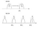
도 1은 통상적인 불휘발성 메모리 장치의 멀티 레벨 셀 프로그램 방법을 설명하기 위한 도면이다.1 is a diagram for describing a multi-level cell program method of a conventional nonvolatile memory device.
하위비트 프로그램(LSB PGM) 동작에서는 프로그램 동작에 의하여 서로 다른 두 개의 셀 분포가 나타난다. 즉, 검증전압(LPV1)이상으로 프로그램된 셀의 분포를 제2 상태라 하고, 그렇지 않은 셀의 분포를 제1 상태라 한다.In the LSB PGM operation, two different cell distributions are displayed by the program operation. That is, the distribution of cells programmed above the verify voltage LPV1 is referred to as a second state, and the distribution of cells not otherwise referred to as a first state.
이렇게 하위비트 프로그램 동작을 수행한 상태에서 상위 비트 프로그램(MSB PGM)동작을 수행하게 된다. 상위 비트 프로그램 동작에서 의하여 서로 다른 문턱전압을 갖는 네 개의 셀 분포(제3 내지 제6 상태)가 나타난다. 이때, 각 분포별로 검증 전압이 상이한바, 낮은 순서부터 정렬하면, 제1 검증전압(MPV1), 제2 검증전압(MPV2), 제3 검증전압(MPV3)을 들 수 있다. 즉, 제3 검증전압(MPV3)이상으로 프로그램된 상태를 제6 상태, 제3 검증전압보다 낮으나 제2 검증전압(MPV2)이상으로 프로그램된 상태를 제5 상태, 제2 검증전압보다 낮으나 제1 검증전압(MPV1)이상으로 프로그램된 상태를 제4 상태, 제1 검증전압보다 낮게 프로그램된 상태를 제3 상태라 한다. 또한, 상기 제4 상태로 프로그램하고자 하는 셀들을 제1 검증 대상 셀, 제5 상태로 프로그램하고자 하는 셀들을 제2 검증 대상 셀, 제6 상태로 프로그램하고자 하는 셀들을 제3 검증 대상 셀로 정의한다.In this state, the lower bit program operation is performed and the upper bit program (MSB PGM) operation is performed. In the upper bit program operation, four cell distributions (third to sixth states) having different threshold voltages appear. In this case, since the verification voltages are different for each distribution, the first verification voltage MPV1, the second verification voltage MPV2, and the third verification voltage MPV3 may be listed in a lower order. That is, the state programmed above the third verify voltage MPV3 is lower than the sixth state and the third verify voltage, but the state programmed above the second verify voltage MPV2 is lower than the fifth state and the second verify voltage, but the first state is lower than the first verify voltage MPV3. A state programmed above the verify voltage MPV1 is referred to as a fourth state, and a state programmed below the first verify voltage is referred to as a third state. In addition, the cells to be programmed to the fourth state are defined as a first verification target cell, the cells to be programmed to a fifth state are second verification target cells, and cells to be programmed to a sixth state are defined as third verification target cells.
이와 같이 상위비트 프로그램 동작에서는 하위비트 프로그램 동작에 비하여 더 많은 검증전압을 기준으로 검증동작을 수행하여야 한다.
As described above, in the higher bit program operation, the verify operation should be performed based on more verification voltages than in the lower bit program operation.
도 2는 통상적인 불휘발성 메모리 장치의 ISPP 프로그램 방법의 개념을 설명하기 위한 도면이다.2 is a diagram for describing a concept of an ISPP program method of a conventional nonvolatile memory device.
ISPP(Incremental step pulse program) 프로그램 방법에 따르면, 프로그램 펄스를 반복하여 인가하되, 매 반복 시마다 검증동작을 수행하고, 프로그램 펄스를 스텝 전압(Vstep) 만큼 증가시켜 인가한다.According to the ISPP (Incremental step pulse program) program method, the program pulse is repeatedly applied, the verification operation is performed at every repetition, and the program pulse is increased by the step voltage Vstep.
도시된 바와 같이, 최초에는 프로그램 시작 전압(Vstart)을 인가하고, 다음 프로그램 펄스 인가시에는 스텝 전압(Vstep) 만큼 증가된 프로그램 펄스를 인가한다. 그리고 매 프로그램 펄스의 인가시마다 검증 동작을 수행한다. 따라서 한번의 프로그램 펄스에 인가에 소요되는 시간은 프로그램 펄스 인가시간(tPULSE)과 검증시간(tVFY)의 합과 같다.As shown, a program start voltage Vstart is first applied, and a program pulse increased by the step voltage Vstep is applied when a next program pulse is applied. The verification operation is performed every time the program pulse is applied. Therefore, the time required to apply one program pulse is equal to the sum of the program pulse application time tPULSE and the verification time tVFY.
한편, 소거 상태의 셀들에 대하여 프로그램 시작전압(Vstart)을 최초로 인가할 경우 셀들의 분포를 고유 분포(△Vthi)라 정의한다. 도면에서는 고유 분포가 대략 4V인 경우가 도시되어 있다. 프로그램 시작전압(Vstart), 스텝 전압(Vstep), 제1 검증전압(PV1)을 기준으로 프로그램 동작을 수행하면, 각 문턱전압이 제1 검증전압(PV1) 이상이고 고유 분포(△Vthi)의 최대값보다 낮은 셀들의 분포가 형성된다. 이때 프로그램이 완료된 셀들의 분포는 스텝 전압(Vstep)의 크기와 같다.Meanwhile, when the program start voltage Vstart is first applied to the cells in the erased state, the distribution of the cells is defined as intrinsic distribution ΔVthi. In the figure, the case where the intrinsic distribution is approximately 4V is shown. When the program operation is performed based on the program start voltage Vstart, the step voltage Vstep, and the first verify voltage PV1, each threshold voltage is equal to or greater than the first verify voltage PV1 and the maximum value of the intrinsic distribution ΔVthi. A distribution of cells lower than the value is formed. At this time, the distribution of the cells in which the program is completed is equal to the magnitude of the step voltage Vstep.
이론적으로는, 프로그램 동작의 완료에 필요한 펄스 인가횟수(Npgm)는 고유분포(△Vthi)와 스텝 전압(Vstep)의 비에 의하여 결정된다. 예를 들어, 고유 분포(△Vthi)가 4V이고, 스텝 전압(Vstep)이 1V 이면 총 4회의 펄스가 인가되어야 한다.Theoretically, the number of pulse application times Npgm necessary for the completion of the program operation is determined by the ratio of the eigendistribution? Vthi and the step voltage Vstep. For example, if the intrinsic distribution ΔVthi is 4V and the step voltage Vstep is 1V, a total of four pulses should be applied.
전체 프로그램 동작에 소요되는 시간(tPROG)은 상기 펄스 인가횟수(Npgm)와 한번의 프로그램 펄스에 인가에 소요되는 시간(tPULSE+tVFY)의 곱과 같다.The time tPROG required for the entire program operation is equal to the product of the pulse application frequency Npgm and the time required for application to one program pulse (tPULSE + tVFY).
이와 같은 ISPP 프로그램 특성에 따르면, 스텝전압(Vstep)을 증가시킬수록 펄스 인가횟수(Npgm)가 감소하므로, 전체 프로그램 동작에 소요되는 시간(tPROG)은 감소된다. 그러나 프로그램이 완료된 셀들의 분포는 스텝전압(Vstep)과 같으므로, 전체 분포가 넓어지게 되는 문제가 발생한다.
According to this ISPP program characteristic, as the step voltage Vstep is increased, the number of pulse application times Npgm decreases, so that the time tPROG required for the entire program operation is reduced. However, since the distribution of the cells in which the program is completed is equal to the step voltage Vstep, the entire distribution becomes wider.
도 3은 통상적인 ISPP 프로그램 방법에서 프로그램 펄스인가에 따른 문턱전압의 이동을 도시한 도면이다.3 is a diagram illustrating a shift of a threshold voltage according to application of a program pulse in a conventional ISPP program method.
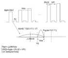
프로그램 시작전압(Vstar)이 16V이고 스텝전압(Vstep)이 1V, 고유 분포(△Vthi)가 4V라고 가정한다. 프로그램하고자 하는 목표전압은 1V~2V이며, 검증전압은 1V 이다.Assume that the program start voltage Vstar is 16V, the step voltage Vstep is 1V, and the intrinsic distribution DELTA Vthi is 4V. The target voltage to be programmed is 1V ~ 2V, and the verification voltage is 1V.
최초 프로그램 펄스인가시의 프로그램 전압(Vpgm)은 16V가 된다. 최초 프로그램 펄스 인가시에는 상기 고유 분포(△Vthi)에 따라 각 셀들의 문턱전압이 결정된다. 상기 최초 프로그램 펄스 인가이후 1V 이상으로 프로그램 된 셀들은 페이지 버퍼에 저장된 데이터가 변경되어, 이후 프로그램 펄스가 더 이상 인가되지 않는다.The program voltage Vpgm at the first program pulse application is 16V. When the first program pulse is applied, the threshold voltages of the cells are determined according to the intrinsic distribution ΔVthi. Cells programmed to 1 V or more after the initial program pulse application are changed in the data stored in the page buffer, so that the program pulse is no longer applied.
두 번째 프로그램 펄스 인가시에, 1V 보다 문턱전압이 낮은 셀들은 프로그램 펄스 인가로 인해 문턱전압이 더욱 상승한다. 바람직하게는 1V 보다 문턱전압이 낮은 셀들이 1V씩 문턱전압이 상승하게 된다. 최초 프로그램 펄스 인가시의 셀들의 분포가 전체적으로 1V 만큼 상승했음을 알 수 있다. 다만 앞서 언급한바와 같이 최초 프로그램 펄스 시 1V이상으로 프로그램 된 셀들에 대해서는 프로그램 펄스가 더 인가되지 않으므로 문턱전압의 변화가 없다.When the second program pulse is applied, the cells having a threshold voltage lower than 1 V further increase the threshold voltage due to the application of the program pulse. Preferably, the threshold voltage increases by 1V for cells having a threshold voltage lower than 1V. It can be seen that the distribution of cells during the initial program pulse application increased by 1V as a whole. However, as mentioned above, since the program pulse is not applied to the cells programmed above 1V during the initial program pulse, there is no change in the threshold voltage.
세 번째, 네 번째 프로그램 펄스 인가시에도 상기와 마찬가지로 1V 씩 문턱전압이 상승하는 것을 알 수 있다. 그리고 프로그램이 완료된 상태의 문턱전압의 분포는 스텝전압의 크기와 같게 된다.
When the third and fourth program pulses are applied, it can be seen that the threshold voltage increases by 1V as above. The threshold voltage distribution in the state where the program is completed is equal to the magnitude of the step voltage.
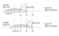
도 4는 통상적인 ISPP 프로그램 방법에서 프로그램 시작전압의 설정에 따른 분포 변화를 도시한 도면이다.4 is a diagram illustrating a distribution change according to setting of a program start voltage in a conventional ISPP program method.
프로그램 시작전압(Vstatr)이 16V 인 경우와 17V 인 경우(고유 분포(△Vthi)는 4V, 스텝 전압(Vstep)은 1V) 프로그램 동작이 완료되었을 때 문턱전압의 분포 상태가 상이해 짐을 알 수 있다. 즉, 프로그램 시작전압이 커지면, 최대 문턱 전압 값이 더욱 커지게 된다. 프로그램 시작전압(Vstatr)이 16V 인 경우의 최대 문턱 전압 값은 2V 이지만, 프로그램 시작전압(Vstatr)이 17V 인 경우의 최대 문턱 전압 값은 3V 가 된다. 이때, 프로그램이 종료된 상태에서의 최대 문턱 전압 값은 상이하지만, 문턱전압의 분포 자체는 1V로 동일함을 알 수 있다. 앞서 언급한 바와 같이 문턱전압의 분포는 스텝 전압(Vstep)에 의해 결정되기 때문이다.When the program start voltage (Vstatr) is 16V and 17V (the unique distribution (△ Vthi) is 4V, the step voltage (Vstep) is 1V), the threshold voltage distribution state is different when the program operation is completed. . In other words, as the program start voltage increases, the maximum threshold voltage value becomes larger. The maximum threshold voltage value is 2V when the program start voltage Vstatr is 16V, but the maximum threshold voltage value is 3V when the program start voltage Vstatr is 17V. At this time, although the maximum threshold voltage value in the program terminated state is different, it can be seen that the distribution of the threshold voltage itself is the same as 1V. As mentioned above, the distribution of the threshold voltages is determined by the step voltage Vstep.
이와 같이 프로그램 시작 전압의 변화에 따라 프로그램이 종료된 상태는 달라지게된다. 이때, 프로그램 펄스 인가횟수 및 프로그램 동작에 소요되는 시간은 동일하다. 이러한 특성에 비추어볼때, 여러 가지 문턱전압 분포 상태를 필요로 하는 MLC 프로그램 동작에서는 하나의 프로그램 시작 전압을 기준으로 프로그램 동작을 수행할 필요가 있다. 즉, 목표로하는 문턱전압이 가장 낮은 셀을 기준으로 프로그램 시작 전압을 설정하여야 오버 프로그램을 방지할 수 있다.As described above, the end state of the program is changed according to the change of the program start voltage. At this time, the program pulse application frequency and the time required for the program operation are the same. In view of these characteristics, it is necessary to perform a program operation based on one program start voltage in an MLC program operation requiring various threshold voltage distribution states. In other words, the program start voltage should be set based on the cell having the lowest target voltage to prevent overprogramming.
예를 들어, 목표로 하는 문턱전압이 1V~2V인 경우, 17V를 프로그램 시작전압으로 설정하게 되면, 도시된 바와 같이 한번의 프로그램 펄스 인가로 2V~3V의 문턱전압을 갖는 셀이 발생하는바, 이러한 셀들은 오버 프로그램 된 것으로 본다. 따라서 16V를 프로그램 시작전압으로 설정하여 프로그램 동작을 수행한다.
For example, when the target threshold voltage is 1V to 2V, when 17V is set as the program start voltage, a cell having a threshold voltage of 2V to 3V is generated by applying one program pulse as shown. These cells are considered to be over programmed. Therefore, set the 16V as the program start voltage and perform the program operation.
도 5는 프로그램 소거 동작횟수에 따른 불휘발성 메모리 장치의 프로그램 속도 변화의 개념을 도시한 도면이다.5 is a diagram illustrating a concept of a program speed change of a nonvolatile memory device according to the number of program erase operations.
불휘발성 메모리 장치를 사용하게 되면, 프로그램 동작과 소거 동작을 수회 반복하게 된다. 이때 프로그램 동작은 페이지 단위로, 소거 동작은 블록 단위로 진행된다. 프로그램/소거 동작 횟수가 증가할수록 불휘발성 메모리 장치의 프로그램 속도가 빨라지는 경향이 있다. 즉, 프로그램/소거 동작 횟수의 증가에 따라 불휘발성 메모리 셀의 플로팅 게이트에 트랩되는 차지의 양이 증가하므로, 일반 셀들에 비하여 프로그램 속도가 증가한다. 이 때 프로그램 속도는 한 번의 프로그램 펄스 인가에 따른 문턱 전압의 변화량으로 정의될 수 있다.When the nonvolatile memory device is used, the program operation and the erase operation are repeated several times. In this case, the program operation is performed in units of pages, and the erase operation is performed in units of blocks. As the number of program / erase operations increases, the program speed of the nonvolatile memory device tends to increase. That is, the amount of charge trapped in the floating gate of the nonvolatile memory cell increases with the increase in the number of program / erase operations. Thus, the program speed is increased compared to the normal cells. In this case, the program speed may be defined as an amount of change in the threshold voltage according to one application pulse application.
따라서 ISPP의 프로그램 펄스 인가 횟수(Npgm)를 결정하는 요소인 고유분포(△Vthi)에 프로그램/소거 횟수 증가에 따른 변화량을 추가하여 고려해야 한다. 이때 상기 변화량은 프로그램/소거 횟수가 증가할수록 커지게 된다.Therefore, the amount of change due to the increase in the number of programs / erases should be considered in addition to the eigendistribution ΔVthi, which is a factor that determines the program pulse application number Npgm. In this case, the amount of change becomes larger as the number of programs / erases increases.
이러한 특성을 고려하여 프로그램 시작전압을 설정한다면, 프로그램/소거 횟수가 최소일 경우에 비하여 프로그램 시작전압을 낮게 설정하여야 한다. 즉, 불휘발성 메모리 장치의 최초 동작시부터 프로그램/소거 횟수 증가에 따른 프로그램 속도를 고려하여 프로그램 시작전압을 낮게 인가하는 것이다. 이러한 구성에 따른다면, 최초 동작시부터 특정 프로그램/소거 횟수 도달전까지는 실질적으로 더미(dummy) 프로그램 펄스를 인가하게 되는 효과가 발생하므로, 전체적으로 프로그램 동작에 소요되는 시간이 증가하게 되는 문제점이 발생한다.
If the program start voltage is set in consideration of these characteristics, the program start voltage should be set lower than the minimum number of program / erase cycles. That is, the initial start voltage of the nonvolatile memory device is applied in consideration of the program speed according to the increase in the number of program / erase times. According to such a configuration, since the effect of applying a dummy program pulse substantially occurs from the first operation until the specific program / erase count is reached, the problem that the time required for the program operation is increased as a whole occurs. .
도 6은 통상적인 불휘발성 메모리 장치의 검증 방법 중 블라인드 검증 방법의 개념을 설명하기 위한 도면이다.6 is a view for explaining the concept of the blind verification method of the verification method of a conventional nonvolatile memory device.
상기 검증 방법은 MLC 프로그램 방법에 적용된다. 도시된 검증 방법은 2비트 멀티 레벨 셀 프로그램시의 검증 방법이다. 총 세 개의 검증 전압(PV1, PV2, PV3)을 기준으로 검증 동작을 수행한다. 상기 세 개의 검증 전압을 기준으로 각각 검증 동작을 수행하므로, 원칙적으로는 한번의 프로그램 펄스 인가 후 세 번의 검증 동작을 수행하여야 한다.The verification method is applied to the MLC program method. The illustrated verification method is a verification method for 2-bit multi-level cell programming. The verification operation is performed based on the three verification voltages PV1, PV2, and PV3. Since each verification operation is performed based on the three verification voltages, in principle, three verification operations should be performed after one program pulse is applied.
그러나 앞서 언급한 바와 같이 프로그램 시작전압은 문턱전압이 제일 낮은 상태를 기준으로 설정되므로, 최초 프로그램 펄스 인가시에는 제2 검증 전압(PV2)및 제3 검증 전압(PV3)이상으로 프로그램되는 셀은 발생하지 않게 된다. 즉, 프로그램 펄스가 어느 정도 인가된 후에야 제2 검증 전압, 제3 검증 전압 이상으로 프로그램 되는 셀들이 발생하게 된다. 따라서 검증 동작에서 소요되는 시간을 단축시키기 위해, 최초 몇 구간 동안은 프로그램 펄스 후 제1 검증 전압을 기준으로 한 검증 동작만을 수행한다. 이와 같이 일부 검증 동작을 생략한다 하여 블라인드(blind) 검증 방법이라 한다. 다만, 이와 같은 블라인드 검증 방법의 개념에 더하여, 앞서 설명한 프로그램/소거 검증 횟수에 따른 프로그램 속도 변화를 고려한 프로그램 펄스 인가방법을 적용할 경우 다음과 같은 문제점이 발생한다.
However, as mentioned above, since the program start voltage is set based on the state where the threshold voltage is lowest, a cell programmed above the second verify voltage PV2 and the third verify voltage PV3 occurs when the first program pulse is applied. You will not. That is, only after the program pulse is applied to some extent, cells programmed above the second verify voltage and the third verify voltage are generated. Therefore, in order to shorten the time required for the verification operation, only the verification operation based on the first verification voltage is performed after the program pulse during the first few sections. As such, some verification operations are omitted, and thus, a blind verification method is described. However, in addition to the concept of the blind verification method, the following problem occurs when the program pulse application method considering the program speed change according to the program / erase verification count described above is applied.
도 7은 통상적인 불휘발성 메모리 장치의 상위 비트 프로그램에 대한 프로그램/검증방법을 설명하기 위한 도면이다.FIG. 7 is a diagram for describing a program / verification method for an upper bit program of a conventional nonvolatile memory device.
제1 프로그램/검증방법에 따르면, 앞서 설명한 블라인드 검증 방법에 따라 최초 프로그램 전압인가 후에 제1 검증전압(MPV1)을 기준으로 하는 검증동작만을 실시한다. 원칙적으로는 제2 검증전압, 제3 검증전압등을 기준으로 하는 검증동작도 같이 실시하여야 하나, 앞서 설명한 블라인드 검증 방법에 따라 제1 검증전압을 기준으로 하는 검증동작만 실시한다.According to the first program / verification method, only the verification operation based on the first verification voltage MPV1 is performed after the initial program voltage is applied according to the blind verification method described above. In principle, the verification operation based on the second verification voltage, the third verification voltage, etc. should also be performed, but only the verification operation based on the first verification voltage is performed according to the blind verification method described above.
프로그램 펄스 인가 및 제1 검증전압을 기준으로 하는 검증동작만을 3회 정도 실시한 후에, 제1 검증전압뿐만 아니라 제2 검증전압을 기준으로 하는 검증동작도 실시한다. 또한, 제1 및 제2 검증전압을 기준으로 하는 검증동작을 3 회 정도 실시한 후에 제3 검증전압을 기준으로 한 검증동작을 실시한다. 한편, 제1 검증전압만을 기준으로 하는 검증동작이 실시되는 횟수, 제1 및 제2 검증전압만을 기준으로 하는 검증동작이 실시되는 횟수는 미리 설정되어 있다.
After only three times of the verification operation based on the program pulse application and the first verification voltage, the verification operation based on the second verification voltage as well as the first verification voltage is also performed. In addition, after performing the verification operation based on the first and second verification voltages about three times, the verification operation based on the third verification voltage is performed. On the other hand, the number of times that the verification operation based on only the first verification voltage is performed and the number of times the verification operation based on only the first and second verification voltage are performed are set in advance.
다음으로 제2 프로그램/검증방법에 대하여 살펴보자. 상기 제2 프로그램/검증 방법은 프로그램/소거 횟수의 증가에 따라 프로그램 속도가 증가하는 경향을 보상하기 위하여 프로그램 시작 펄스를 낮춰서 인가한다. 즉, 도시된 바와 같이 제1 프로그램/검증 방법에 비하여 프로그램 시작 펄스를 낮춰서 인가하게 된다. 다만, 이는 프로그램/소거 횟수에 따라 문제점을 나타낼 수 있다.Next, let's look at the second program / validation method. The second program / verification method applies a lower program start pulse to compensate for the tendency of the program speed to increase as the number of programs / erases increases. That is, as shown, the program start pulse is lowered and applied as compared to the first program / verification method. However, this may indicate a problem depending on the number of programs / erases.
즉, 프로그램/소거 횟수가 높은 경우에는 프로그램 속도가 빠르기 때문에 낮은 프로그램 펄스의 인가에도 문턱전압의 변화량이 크다. 따라서 낮은 프로그램 전압의 인가시에도 검증동작을 수행할 필요가 있다. 또한, 문턱전압이 일부 상승한 시점이후(A 이후)에는 제1 및 제2 검증전압을 기준으로 한 검증동작을 실시할 필요가 있다.In other words, when the program / erase number is high, the program speed is high, so the amount of change in the threshold voltage is large even when a low program pulse is applied. Therefore, it is necessary to perform the verification operation even when the low program voltage is applied. In addition, it is necessary to perform a verification operation on the basis of the first and second verification voltages after a time when the threshold voltage partially rises (after A).
그러나 프로그램/소거 횟수가 작은 경우에는 프로그램 속도가 늦기 때문에 낮은 프로그램 펄스의 인가에 대한 문턱전압의 변화량이 작은 편이다. 따라서 낮은 프로그램 전압의 인가시에 검증동작을 수행해야할 필요는 적어진다. 또한, 문턱전압의 상승 폭이 작기 때문에, 프로그램 펄스가 어느 정도 인가된 이후(A 이후)에도 제1 검증전압을 기준으로 한 검증동작 이외에 제2 검증전압을 기준으로 한 검증동작까지 실시해야할 필요는 적어진다.
However, when the number of program / erase times is small, the program speed is slow, so the amount of change in the threshold voltage for application of a low program pulse is small. Therefore, there is less need to perform the verify operation when applying a low program voltage. In addition, since the rising width of the threshold voltage is small, it is necessary to perform the verification operation based on the second verification voltage in addition to the verification operation based on the first verification voltage even after the program pulse is applied to some extent (after A). Less.
도 8은 통상적인 불휘발성 메모리 장치의 프로그램/검증방법을 설명하기 위한 도면이다.8 is a diagram for describing a program / verification method of a conventional nonvolatile memory device.
도 8을 참조하면, 통상적인 불휘발성 메모리 장치에서는 다만, 이러한 상태에서 앞서 설명한 블라인드(blind) 검증 방법을 단편적으로 적용할 경우, 프로그램/소거 횟수가 낮은 초기 동작에서는 제1 검증전압을 기준으로 하는 검증 동작외에 불필요하게 제2 검증전압을 기준으로 하는 검증 동작을 실시하게 되는 경우가 존재 한다.Referring to FIG. 8, in the conventional nonvolatile memory device, when the blind verification method described above is partially applied in this state, the first verification voltage may be referred to in the initial operation having a low program / erase frequency. In addition to the verification operation, there is a case where a verification operation based on the second verification voltage is unnecessarily performed.
이를 방지하기 위하여 본원 발명에서는 제1 검증전압 이상으로 프로그램된 셀이 검출된 경우에 한하여 블라인드 검증방법을 적용한다.In order to prevent this, the present invention applies the blind verification method only when a cell programmed above the first verification voltage is detected.
즉, 도시된 바와 같이 제1 검증전압 이상으로 프로그램된 셀이 검출되기 전까지는 제1 검증전압을 기준으로 하는 제1 검증동작과, ISPP 프로그램 동작을 번갈아서 수행한다. 그리고 제1 검증전압 이상으로 프로그램된 셀이 검출되면, 검출될 때까지 인가된 프로그램 펄스 횟수를 저장하였다가 다른 페이지 영역에 프로그램을 수행할 때 저장된 프로그램 펄스 횟수를 기준으로 프로그램 시작전압을 조절하여 상기 설명한 블라인드 검증방법을 수행한다.That is, as shown, the first verification operation based on the first verification voltage and the ISPP program operation are alternately performed until the cell programmed above the first verification voltage is detected. When a cell programmed above the first verification voltage is detected, the program start voltage is stored based on the number of stored program pulses when the program pulse count is stored until the detection is performed and the program is executed in another page area. Perform the blind verification method described.
예컨대, 통상적인 불휘발성 메모리 장치에서는 제1 페이지 영역에 대해 프로그램을 수행하면서 제1 검증전압 이상으로 프로그램된 셀이 검출될 때까지 인가되는 프로그램 펄스 횟수를 카운팅하게 된다. 도 8에서는 제1 페이지 영역에 대한 프로그램 펄스 인가 횟수가 '4'인 것을 알 수 있다. 따라서, 제1 페이지 영역에 대한 프로그램 시작전압에 4배의 스텝전압을 더하여 제2 페이지 영역에 대한 프로그램 시작전압을 설정하고, 설정된 프로그램 시작전압에 따라 제2 페이지 영역에 대한 프로그램 동작을 수행하게 된다. 이와 같이 제1 페이지 영역의 프로그램 결과를 근거로 제2 페이지 영역의 프로그램 시작전압을 가변적으로 설정하므로, 더미 프로그램 펄스의 인가에 소요되는 시간을 단축시킬 수 있다. 즉, 도 8의 경우와 같이 제2 페이지 영역에 대한 프로그램 동작시 네 번의 더미 프로그램 펄스 인가 및 검증동작에 소요되는 시간을 감소시킬 수 있다.For example, in a conventional nonvolatile memory device, the number of program pulses applied until a cell programmed above the first verification voltage is detected while performing a program on a first page area. In FIG. 8, it can be seen that the number of program pulses applied to the first page area is '4'. Therefore, the program start voltage for the second page area is set by adding a four times step voltage to the program start voltage for the first page area, and the program operation for the second page area is performed according to the set program start voltage. . As described above, since the program start voltage of the second page area is variably set based on the program result of the first page area, the time required for applying the dummy program pulse can be shortened. That is, as shown in FIG. 8, the time required for four dummy program pulse application and verification operations during the program operation on the second page area may be reduced.
그런데, 통상적인 불휘발성 메모리 장치에서는 제1 검증전압 이상으로 프로그램된 셀이 검출될 때까지 인가된 프로그램 펄스 횟수를 저장하기 위한 수단으로 컨트롤러에 포함된 래치를 사용하였다.However, in the conventional nonvolatile memory device, a latch included in the controller is used as a means for storing the number of program pulses applied until a cell programmed above the first verification voltage is detected.
즉, 불휘발성 메모리 장치에는 페이지 영역의 개수가 적어도 수십 개에서 수백 개 포함되는 것이 일반적이므로 불휘발성 메모리 장치에 포함된 모든 페이지 영역의 프로그램 펄스 횟수를 저장하기 위해서는 페이지 영역 수에 대응하는 만큼의 래치가 컨트롤러 내부에 존재해야 하는데, 이는 실질적으로 가능한 구성이 아니다.That is, since the number of page areas is generally included in at least tens to hundreds of nonvolatile memory devices, in order to store the number of program pulses of all the page areas included in the nonvolatile memory device, a latch corresponding to the number of page areas is used. Must be present inside the controller, which is not a practically possible configuration.
따라서, 통상적인 불휘발성 메모리 장치에서는 설정된 일부 페이지 영역에 대응하는 소수의 래치를 컨트롤러에 구비한 상태에서 설정된 페이지 영역의 프로그램 동작을 통해 조절가능한 프로그램 시작전압을 설정된 페이지 영역 주변의 다수의 페이지 영역에 일괄적으로 적용하는 방식을 사용하였다.Accordingly, in a conventional nonvolatile memory device, a program start voltage that is adjustable through a program operation of a set page area in a state in which a controller has a small number of latches corresponding to some set page areas is applied to a plurality of page areas around the set page area. The batch application method was used.
하지만, 아무리 근처에 위치한 두 개의 페이지 영역라고 하더라도 두 페이지 영역사이에 공정(Process), 사이클링(cycling)정도 등의 요인으로 어떤 차이가 발생한다면 동일한 값을 적용하였을 때 정상적으로 데이터를 검출할 수 없을 수 있는 문제가 있다. 즉, 아무리 근처에 위치한 두 개의 페이지 영역라고 하더라도 두 페이지 영역 사이의 차이를 감안한 마진(margin)을 두어야 한다.However, even if there are two page areas located nearby, if there is any difference between the two page areas due to the process and the degree of cycling, the data cannot be detected normally when the same value is applied. There is a problem. In other words, even if two page areas are located near each other, margins should be set in consideration of the difference between the two page areas.
예를 들어, 어떤 페이지 영역가 프로그램 동작시 4번의 프로그램 펄스를 인가하는 동작으로 제1 검증전압 이상으로 프로그램된 셀이 검출되더라도 근처의 다른 페이지 영역은 같은 조건에서 이보다 빠른 2번의 프로그램 펄스가 인가되거나 3번의 프로그램 펄스가 인가되는 동작으로 제1 검증전압 이상으로 프로그램된 셀이 존재할 수 있다.For example, if a page region is programmed to apply four program pulses during a program operation, and a cell programmed above the first verification voltage is detected, two other program regions are applied with two faster program pulses under the same conditions. In the operation of applying the program pulse, there may be a cell programmed above the first verification voltage.
즉, 상기에서 설명한 통상적인 불휘발성 메모리 장치의 동작방법은 반도체 칩 또는 동작 계획(plane) 등의 전체 변수를 판단해 마진(margin)을 두어야 하는데 이 마진에 따라 불휘발성 메모리 장치의 프로그램/검증방법 성능에 차이가 발생할 수 있다.That is, in the above-described method of operating a nonvolatile memory device, a margin must be determined by determining a whole variable such as a semiconductor chip or an operation plan, and the program / verification method of the nonvolatile memory device according to this margin. Performance may vary.
도 9는 본 발명의 실시예에 따른 불휘발성 메모리 장치를 도시한 블록 다이어그램이다.9 is a block diagram illustrating a nonvolatile memory device according to an embodiment of the present invention.
도 10은 도 9에 도시된 본 발명의 실시예에 따른 불휘발성 메모리 장치의 메모리 셀 어레이 및 페이지 버퍼링부의 첫 번째 구성을 상세히 도시한 블록 다이어그램이다.FIG. 10 is a detailed block diagram illustrating a first configuration of a memory cell array and a page buffering unit of a nonvolatile memory device according to an exemplary embodiment of the present invention illustrated in FIG. 9.
도 9를 참조하면, 본 발명의 실시예에 따른 불휘발성 메모리 장치는, 불휘발성 메모리 셀 어레이(900)와, 페이지 버퍼링부(910)와, 비트 패스 검출부(920)와, 컨트롤러 내부에 구비되는 프로그램 시작전압 설정부(930)와, 프로그램 펄스 인가횟수 저장부(940)와, 프로그램 펄스 카운팅부(950), 및 고전압 발생기(960)을 구비한다.9, a nonvolatile memory device according to an exemplary embodiment of the present invention includes a nonvolatile
참고로, 그 동작에 따른 구성이 구체적으로 도시되진 않았지만 컨트롤러는 불휘발성 메모리 장치의 프로그램 동작, 독출 동작, 소거 동작등 각종 동작을 수행한다. 외부에서 입력되는 명령어, 어드레스, 데이터등을 입력받아 해당하는 동작을 수행한다. 또한 고전압 발생기(960)를 제어하여 각 동작에 해당하는 고전압(프로그램 전압, 패스전압, 독출전압 등)을 메모리 셀어레이에 인가시킨다. 또한 프로그램 동작시에 수행되는 검증 동작에서는 각 메모리 셀이 기준전압 이상으로 프로그램 되었는지 여부를 확인하는바, 패스 완료신호가 입력되면 프로그램 동작이 종료되도록 제어한다.For reference, although the configuration according to the operation is not specifically illustrated, the controller performs various operations such as program operation, read operation, and erase operation of the nonvolatile memory device. It receives a command, address, data, etc. input from the outside and performs a corresponding operation. In addition, the
즉, 컨트롤러 내부에 도시된 프로그램 시작전압 설정부(930)와 프로그램 펄스 인가횟수 저장부(940)와 프로그램 펄스 카운팅부(950)는 본 발명의 특징적인 동작인 페이지 영역의 프로그램 대상 셀 중 기준전압 이상으로 프로그램이 완료된 셀이 발생한 시점, 즉 1 비트 패스 시점까지 인가된 프로그램 펄스 인가횟수를 측정하고 그에 따라 프로그램 시작전압을 설정하기 위해 필요한 구성요소들이다.That is, the program start
구체적으로, 메모리 셀 어레이(900)와 페이지 버퍼링부(910)의 구체적인 구성을 도시한 도 10을 참조하여 본 발명의 실시예에 따른 불휘발성 메모리 장치의 구성을 설명하면 다음과 같다.Specifically, a configuration of a nonvolatile memory device according to an exemplary embodiment of the present invention will be described with reference to FIG. 10, which shows a detailed configuration of the
먼저, 메모리 셀 어레이(900)는 노말 영역(900A)과 보조 영역(900B)을 포함한다. 마찬가지로, 페이지 버퍼링부(910)는 메모리 셀 어레이(900)의 노말 영역(900A)에 대응하는 노말 페이지 버퍼링부(910A)와 보조 영역(900B)에 대응하는 보조 페이지 버퍼링부(910B)를 포함한다.First, the
여기서, 메모리 셀 어레이(900)의 노말 영역(900A)은 상기에서 설명한 통상적인 불휘발성 메모리 장치의 메인 영역과 스페어 영역 및 리던던시 영역을 모두 아우르는 영역이다. 반면, 메모리 셀 어레이(900)의 보조 영역(900B)은 상기에서 설명한 통상적인 불휘발성 메모리 장치에는 포함되지 않았던 영역이다. 즉, 메모리 셀 어레이(900)의 보조 영역(900B)은 본 발명의 실시예에 따른 불휘발성 메모리 장치를 위해 추가된 영역이며 수 바이트(byte)의 용량을 가질 수 있도록 설계된다. 이때, 메모리 셀 어레이(900)의 보조 영역(900B)은 통상적인 불휘발성 메모리 장치에 완전히 새롭게 추가된 영역으로써 메모리 셀 어레이(900)의 전체 영역 크기를 조금 더 증가시키는 방식으로 통해 구현될 수 있다. 물론, 메모리 셀 어레이(900)의 전체 영역 크기를 증가시키지 않고 상기에서 설명한 통상적인 불휘발성 메모리 장치에 이미 포함되어 있는 스페어 영역 또는 리던던시 영역의 일부 구간을 분할하여 보조 영역(900B)으로서 설정하는 것도 가능하다.In this case, the normal region 900A of the
이렇게, 메모리 셀 어레이(900)가 노말 영역(900A)과 보조 영역(900B)을 포함하기 때문에 메모리 셀 어레이(900)에 구비되어 각각 다수의 셀을 포함하는 다수의 단일 페이지 영역(900<0:K>, 901<0:K>, …)도 다수의 노말 셀(BL<0:M-1>에 대응함)과 다수의 보조 셀(BL<M:N-1>에 대응함)을 포함하는 형태로 구성된다. 즉, 각각의 단일 페이지 영역(900<0:K>, 901<0:K>, …)별로 다수의 노말 셀(BL<0:M-1>에 대응함)과 다수의 보조 셀(BL<M:N-1>에 대응함)을 포함하는 형태가 된다.As such, since the
그리고, 단일 페이지 영역(900<0:K>, 901<0:K>, …)의 프로그램 대상 셀 중 기준전압보다 큰 전압으로 프로그램된 셀이 발생하는 경우 1 비트 패스 신호(1BIT_PASS)를 출력하는 비트 패스 검출부(920)와, 단일 페이지 영역(900<0:K>, 901<0:K>, …)에 대한 제1 프로그램 동작과정에서 1 비트 패스 신호(1BIT_PASS)가 출력되는 시점까지 인가된 프로그램 펄스의 횟수를 다수의 보조 셀(BL<M:N-1>에 대응함)에 저장하는 프로그램 펄스 인가횟수 저장부(940), 및 다수의 보조 셀(BL<M:N-1>에 대응함)에 저장된 프로그램 펄스의 인가횟수를 기초로 하여 단일 페이지 영역(900<0:K>, 901<0:K>, …)의 제2 프로그램 동작에 대한 프로그램 시작전압을 설정하는 프로그램 시작 전압 설정부(930)를 구비한다.When a cell programmed with a voltage greater than the reference voltage is generated among the program target cells of the
또한, 제1 프로그램 동작과정에서 1 비트 패스 신호(1BIT_PASS)가 출력되는 시점까지 단일 페이지 영역(900<0:K>, 901<0:K>, …)으로 인가되는 프로그램 펄스의 횟수를 카운팅하여 프로그램 펄스 인가횟수 저장부(940)로 전달하는 프로그램 펄스 카운팅부(950)를 더 구비한다.In addition, by counting the number of program pulses applied to a
전술한 구성에서 메모리 셀 어레이(900)에 구비된 다수의 셀은 모두 멀티 레벨 셀(Multi Level Cell : MLC)이다. 즉, 단일 페이지 영역(900<0:K>, 901<0:K>, …)에 포함된 다수의 노말 셀(BL<0:M-1>에 대응함)과 다수의 보조 셀(BL<M:N-1>에 대응함)은 모두 멀티 레벨 셀(MLC)이다. 따라서, 본 발명의 실시예에 따른 불휘발성 메모리 장치의 프로그램 동작은 도 11에 도시된 순서도와 같이 제1 프로그램 동작과 제2 프로그램 동작으로 나누어진다. 이때, 제1 프로그램 동작은 예컨대 하위비트 프로그램 동작이 되고 제2 프로그램 동작은 예컨대 상위비트 프로그램 동작이 될 것이다.In the above configuration, the plurality of cells included in the
도 11을 참조하여 본 발명의 실시예에 따른 불휘발성 메모리 장치의 프로그램 동작을 구체적으로 설명하면 다음과 같다.A program operation of a nonvolatile memory device according to an embodiment of the present invention will be described in detail with reference to FIG. 11 as follows.
먼저, 불휘발성 메모리 장치에 파워가 공급(1100)될 때, '초기화된 제1 프로그램 시작전압'과 '초기화된 제2 프로그램 시작전압'은 미리 알 수 있는 값이다. 이때, '초기화된 제1 프로그램 시작전압'과 '초기화된 제2 프로그램 시작전압'은 상기의 도 2에서 설명했던 소거 상태의 셀들에 대하여 최초로 인가되는 프로그램 시작전압(Vstart)라고 볼 수 있으며, 설계자에 의해 그 기본 값(default value)이 조절된다. 참고로, '초기화된 제1 프로그램 시작전압'과 '초기화된 제2 프로그램 시작전압'은 다수의 단위 페이지 영역(900<0:K>, 901<0:K>, …)에 각각 적용될 상수이므로 일반적으로는 서로 같아지도록 그 기본 값(default value)이 조절된다. 물론, '초기화된 제1 프로그램 시작전압'과 '초기화된 제2 프로그램 시작전압'의 기본 값이 같아지도록 조절된다는 것은 어디까지나 설계자의 선택에 의해 변화될 수 있는 사항이므로, 서로 달라지도록 조절되는 것도 얼마든지 가능하다.First, when power is supplied to the
그 후, 어떤 프로그램 동작을 수행할 것인지를 결정(1110)하게 된다. 즉, 제1 프로그램 동작을 수행할 것인지 아니면 제2 프로그램 동작을 수행하게 될 것인지를 선택하게 된다. 이때, 소거 상태의 단일 페이지 영역(900<0:K>, 901<0:K>, …)를 대상으로 프로그램 동작이 수행될 때에는 제1 프로그램 동작을 수행하게 될 것이고, 제1 프로그램 동작이 이미 수행된 이후의 단일 페이지 영역(900<0:K>, 901<0:K>, …)를 대상으로 프로그램 동작이 수행될 때에는 제2 프로그램 동작을 수행하게 될 것이다. 예컨대, 일반적인 불휘발성 메모리 장치에서 소거 상태의 셀을 대상으로 먼저 하위비트 프로그램 동작을 수행되고 이후에 상위비트 프로그램 동작을 수행되는 것과 같다.Thereafter, it is determined 1110 which program operation to perform. That is, it is selected whether to perform the first program operation or the second program operation. At this time, when the program operation is performed on the
먼저, 제1 프로그램 동작을 설명하면, '초기화된 제1 프로그램 시작전압'이 단일 페이지 영역(900<0:K>, 901<0:K>, …)으로 공급(1120)하게 되고, 이어서 1 비트 패스가 검출되었는지 확인(1122)한다. 이때, 1 비트 패스가 검출되지 않았다면 '초기화된 제1 프로그램 시작전압'에'스텝전압'을 합한 전압을 단일 페이지 영역(900<0:K>, 901<0:K>, …)으로 다시 공급(1120)하게 되고, 이어서 다시 1 비트 패스가 검출되었는지 확인(1122)한다. 또 다시 1 비트 패스가 검출되지 않았다면 '초기화된 제1 프로그램 시작전압'에'스텝전압 * 2 '를 합한 전압을 단일 페이지 영역(900<0:K>, 901<0:K>, …)으로 다시 공급(1120)하게 되고, 이어서 다시 1 비트 패스가 검출되었는지 확인(1122)한다.First, when the first program operation is described, the 'initialized first program start voltage' is supplied to the
이와 같이 단일 페이지 영역(900<0:K>, 901<0:K>, …)에 프로그램 전압을 공급하는 동작(1120)과 1 비트 패스가 검출되었는지 확인하는 동작(1122)를 계속 반복하면서 단일 페이지 영역(900<0:K>, 901<0:K>, …)에 공급되는 프로그램 전압의 크기를 '스텝전압 * N'(N = 반복횟수)씩 증가시킨다. 즉, '초기화된 제1 프로그램 시작전압'을 기준으로 일반적인 ISPP동작을 수행하면서 1 비트 패스가 검출되었는지 확인하는 동작(1122)을 계속 수행한다.As described above, the
이렇게, 단일 페이지 영역(900<0:K>, 901<0:K>, …)에 프로그램 전압을 공급하는 동작(1120)과 1 비트 패스가 검출되었는지 확인하는 동작(1122)를 계속 반복되다가 1 비트 패스가 검출되는 경우, 프로그램 펄스 카운팅부(950)에서 출력되는 1 비트 패스가 검출되기까지 카운팅된 프로그램 펄스 횟수(PD)를 프로그램 펄스 인가횟수 저장부(940)를 통해 단일 페이지 영역(900<0:K>, 901<0:K>, …)의 보조 페이지 버퍼링부(910B)에 셋팅(1124)하고 이어서 제1 프로그램 동작을 계속 수행(1126)하여 제1 프로그램 동작이 완료(1150)될 수 있도록 한다.In this manner, the
이와 같이, 프로그램 펄스 인가횟수 저장부(940)가 프로그램 펄스 카운팅부(950)에서 출력되는 1 비트 패스가 검출되기까지 카운팅된 프로그램 펄스 횟수(PD)를 보조 페이지 버퍼링부(910B)에 셋팅한 후 제1 프로그램 동작을 수행을 완료하게 되면, 보조 페이지 버퍼링부(910B)에 대응하는 다수의 보조 셀(BL<M:N-1>에 대응함)에 프로그램 펄스 카운팅부(950)에서 출력되는 1 비트 패스가 검출되기까지 카운팅된 프로그램 펄스 횟수(PD)가 저장된다는 것을 알 수 있다.As described above, the program pulse application
또한, 다수의 단위 페이지 영역(900<0:K>, 901<0:K>, …)은 각각 다수의 노말 셀(BL<0:M-1>에 대응함)과 다수의 보조 셀(BL<M:N-1>에 대응함)을 구비하고 있으므로, 각 단위 페이지 영역(900<0:K>, 901<0:K>, …)의 다수의 보조 셀(BL<M:N-1>에 대응함)에는 각각의 단위 페이지 영역(900<0:K>, 901<0:K>, …)에 대응하는 1 비트 패스가 검출되기 까지 카운팅된 프로그램 펄스 횟수(PD)가 독립적으로 저장되는 것을 알 수 있다.Further, the plurality of
참고로, 전술한 제1 프로그램 동작에는 도 9에 도시된 컨트롤러 내부의 프로그램 펄스 카운팅부(950)와 프로그램 펄스 인가횟수 저장부(940)가 대응될 것이다. 즉, 일반적인 ISPP 동작을 수행하는 회로는 도 9에 도시된 컨트롤러에 이미 포함되어 있고 도시되지 않았다는 것을 알 수 있다.For reference, the above-described first program operation may correspond to the program
그리고, 제2 프로그램 동작을 설명하면, 제1 프로그램 동작이 완료되어 1 비트 패스가 검출되기까지 카운팅된 프로그램 펄스 횟수(PD)가 다수의 보조 셀(BL<M:N-1>에 대응함)에 저장된 단위 페이지 영역에서 제2 프로그램 동작이 수행되어야 하기에 '초기화된 제2 프로그램 시작전압'을 공급하기 전에 먼저 다수의 보조 셀(BL<M:N-1>에 대응함)에 저장된 1 비트 패스가 검출되기까지 카운팅된 프로그램 펄스 횟수(PD)를 리드(1140)한다.In the following description of the second program operation, the number of program pulses PD counted until the first program operation is completed and one bit path is detected corresponds to the plurality of auxiliary cells BL <M: N-1>. Since the second program operation must be performed in the stored unit page area, the 1-bit path stored in the plurality of auxiliary cells (corresponding to BL <M: N-1>) is first loaded before the 'initialized second program start voltage' is supplied. The number of program pulses PD counted until detected is read 1140.
리드된 1 비트 패스가 검출되기까지 카운팅된 프로그램 펄스 횟수(PD)를 '초기화된 제2 프로그램 시작전압'에 적용하는 것은 도 9에 도시된 프로그램 시작전압 설정부(930)에 의해 이루어지는데, 그 방식은 다음과 같이 두 가지로 나뉘어 질 수 있다.Applying the counted program pulse number PD to the 'initialized second program start voltage' until the read one bit path is detected is made by the program start
첫 번째는, 다수의 보조 셀(BL<M:N-1>에 대응함)에 저장된 프로그램 펄스의 인가횟수(PD)를 리드한 뒤, 리드된 프로그램 펄스의 인가횟수(PD)에 '스텝전압'을 곱한 값을 '초기화된 제2 프로그램 시작전압'의 값에 더하여 새로운 '제2 프로그램 시작전압'으로서 설정(1142)하게 된다.First, after the number of times of application pulses PD stored in the plurality of auxiliary cells (corresponding to BL <M: N-1>) is read, the 'step voltage' is applied to the number of times of application pulses read. The multiplied value is added to the value of the 'initialized second program start voltage' and set as a new 'second program start voltage' 1114.
두 번째는, 다수의 보조 셀(BL<M:N-1>에 대응함)에 저장된 프로그램 펄스의 인가횟수(PD)를 리드한 뒤, 리드된 프로그램 펄스의 인가횟수(PD)가 임계값보다 큰 경우 리드된 프로그램 펄스 인가횟수(PD)와 임계값의 차이만큼 '스텝전압'을 곱한 값을 '초기화된 제2 프로그램 시작전압'의 값에 더하여 새로운 '제2 프로그램 시작전압'으로서 설정(1142)한다. 하지만, 리드된 프로그램 펄스의 인가횟수(PD)가 임계값보다 작거나 같은 경우 '초기화된 제2 프로그램 시작전압'을 그대로 '제2 프로그램 시작전압'으로서 설정(1142)하게 된다. 이때. 임계값은 셀의 특성등에 따라 실시자에 의해 최적의 값으로 선택될 수 있다. 예컨대, 리드된 프로그램 펄스의 인가횟수(PD)가 '2'보다 작은 값이면 큰 의미가 없다고 판단하여 '2'를 임계값으로 설정할 수 있다.Second, after the application frequency PD of the program pulse stored in the plurality of auxiliary cells (corresponding to BL <M: N-1>) is read, the application frequency PD of the read program pulse is greater than the threshold value. In this case, the value obtained by multiplying the step voltage is multiplied by the difference between the number of times of the applied program pulse PD and the threshold value is set as a new second program start voltage by adding the value of the initialized second program start voltage 1114. do. However, when the number of times PD of the read program pulses is less than or equal to the threshold value, the initializing second program start voltage is set as the second program start voltage 1114. At this time. The threshold value may be selected as an optimal value by the operator according to the characteristics of the cell. For example, if the number of times of application of the read program pulse PD is smaller than '2', it is determined that there is no significant meaning, so that '2' may be set as a threshold.
이와 같이 리드된 1 비트 패스가 검출되기까지 카운팅된 프로그램 펄스 횟수(PD)를 '초기화된 제2 프로그램 시작전압'에 적용하는 방법 통해 결정된 새로운 '제2 프로그램 시작전압'을 공급받아 제2 프로그램 동작이 수행된다. 이때, 제2 프로그램 동작은 새로운 '제2 프로그램 시작전압'을 공급받기 때문에 제1 프로그램 동작보다 더 빠른 타이밍에 프로그램 동작을 완료하는 것이 가능하다. 참고로, 제2 프로그램 동작도 일반적인 ISPP 방식을 사용하여 동작한다.The second program operation is supplied by receiving a new 'second program start voltage' determined by applying the counted program pulse number PD to the 'initialized second program start voltage' until the read one bit path is detected. This is done. At this time, since the second program operation is supplied with a new 'second program start voltage', it is possible to complete the program operation at a faster timing than the first program operation. For reference, the second program operation also operates using a general ISPP method.
전술한 도 9 내지 도 11을 통해 단일 페이지 영역(900<0:K>, 901<0:K>, …)를 프로그램 시킬 때 하위비트 프로그램 동작이 발생하는 과정에서 단일 페이지 영역(900<0:K>, 901<0:K>, …)의 특성에 적합한 초기 시작전압을 찾아내기 위해 필요한 정보 - 1 비트 패스가 검출되기까지 카운팅된 프로그램 펄스 횟수(PD)임 - 를 내부에 포함된 다수의 보조 셀에 저장할 수 있다. 이렇게 내부의 다수의 보조 셀에 저장된 단일 페이지 영역(900<0:K>, 901<0:K>, …)의 특성에 적합한 초기 시작전압을 찾아내기 위해 필요한 정보는 상위비트 프로그램 동작이 발생하는 과정에서 사용되어 상위비트 프로그램 동작에 걸리는 시간을 크게 단축시킬 수 있다.9 to 11, the
또한, 단일 페이지 영역(900<0:K>, 901<0:K>, …) 내부의 다수의 보조 셀에 저장된 단일 페이지 영역(900<0:K>, 901<0:K>, …)의 특성에 적합한 초기 시작전압을 찾아내기 위해 필요한 정보는 불휘발성 메모리 장치에 전원이 공급되지 않는 상황에서도 지워지지 않는다. 따라서, 하위비트 프로그램 동작이 발생한 이후 전원공급이 끊어졌다가 다시 공급되더라도 상위비트 프로그램 동작이 발생하는 과정에서 사용되어 상위비트 프로그램 동작에 걸리는 시간을 크게 단축시킬 수 있다. 마찬가지로, 단일 페이지 영역(900<0:K>, 901<0:K>, …) 내부의 다수의 노말 셀(BL<0:M-1>에 대응함)에 대한 소거 동작과 다수의 보조 셀(BL<M:N-1>에 대응함)에 대한 소거 동작을 서로 다른 방식으로 컨트롤할 수 있다면, 불휘발성 메모리 장치의 동작 초기에 다수의 단일 페이지 영역(900<0:K>, 901<0:K>, …) 각각의 특성에 적합한 초기 시작전압을 찾아내어 내부의 다수의 보조 셀(BL<M:N-1>에 대응함)에 저장한 다음 이후의 모든 프로그램 동작에 적용하는 것도 가능하다. 즉, 다수의 노말 셀(BL<0:M-1>에 대응함) 및 다수의 보조 셀(BL<M:N-1>에 대응함)이 멀티 레벨 셀(Multi Level Cell : MLC)인 경우 뿐만 아니라 싱글 레벨 셀(Single Level Cell : SLC)라고 하여도 그 프로그램 동작 속도를 단축시키는데 본 발명의 아이디어가 적용될 수 있다.
Further, a
도 12는 도 9에 도시된 본 발명의 실시예에 따른 불휘발성 메모리 장치의 메모리 셀 어레이 및 페이지 버퍼링부의 두 번째 구성을 상세히 도시한 블록 다이어그램이다.FIG. 12 is a detailed block diagram illustrating a second configuration of a memory cell array and a page buffering unit of a nonvolatile memory device according to an exemplary embodiment of the present invention illustrated in FIG. 9.
참고로, 도 12에 도시된 도면은 전술한 도 10과 마찬가지로 도 9에 도시된 불휘발성 메모리 장치의 구성요소 중 메모리 셀 어레이(900)와 페이지 버퍼링부(910)의 구체적인 구성을 도시한 도면이라는 것을 알 수 있다. 다만, 도 10에 도시된 메모리 셀 어레이(900)의 구체적인 구성이 도 10에 도시된 도면과 큰 차이점을 갖기 때문에 그 전반적인 동작도 차이가 발생할 수 있으며, 이하에서 개시될 도 12에 대한 설명에서는 도 10과 도 12의 차이점을 기준으로 설명이 이루어질 것이다.For reference, FIG. 12 is a diagram illustrating a detailed configuration of the
도 12를 참조하면, 본 발명의 실시예에 따른 불휘발성 메모리 장치의 메모리 셀 어레이(900)는, 노말 영역(900C)와 보조 영역(900D)를 포함한다. 마찬가지로, 페이지 버퍼링부(910)는 메모리 셀 어레이(900)의 노말 영역(900C)에 대응하는 노말 페이지 버퍼링부(910C)와 보조 영역(900D)에 대응하는 보조 페이지 버퍼링부(910D)를 포함한다.Referring to FIG. 12, a
여기서, 메모리 셀 어레이(900)의 노말 영역(900C)은 상기에서 설명한 통상적인 불휘발성 메모리 장치의 메인 영역과 스페어 영역 및 리던던시 영역을 모두 아우르는 영역이다. 반면, 메모리 셀 어레이(900)의 보조 영역(900D)은 상기에서 설명한 통상적인 불휘발성 메모리 장치에는 포함되지 않았던 영역이다. 즉, 메모리 셀 어레이(900)의 보조 영역(900D)은 본 발명의 실시예에 따른 불휘발성 메모리 장치를 위해 추가된 영역이며 수 바이트(byte)의 용량을 가질 수 있도록 설계된다. 이때, 메모리 셀 어레이(900)의 보조 영역(900D)은 통상적인 불휘발성 메모리 장치에 완전히 새롭게 추가된 영역으로써 메모리 셀 어레이(900)의 전체 영역 크기를 조금 더 증가시키는 방식으로 통해 구현될 수 있다. 물론, 메모리 셀 어레이(900)의 전체 영역 크기를 증가시키지 않고 상기에서 설명한 통상적인 불휘발성 메모리 장치에 이미 포함되어 있는 스페어 영역 또는 리던던시 영역의 일부 구간을 분할하여 보조 영역(900D)으로서 설정하는 것도 가능하다.In this case, the normal region 900C of the
이렇게, 메모리 셀 어레이(900)가 노말 영역(900C)과 보조 영역(900D)을 포함하기 때문에 메모리 셀 어레이(900)에 구비되어 각각 다수의 셀을 포함하며 서로 워드라인(WL<0:K>)을 공유하는 제1 페이지 영역(900<E0:EK>, 901<E0:EK>, …) 및 제2 페이지 영역(900<O0:OK>, 901<O0:OK>, …)도 각각 다수의 노말 셀(BLE<0:M-1> 및 BLO<0:M-1>에 대응함)과 다수의 보조 셀(BLE<M:N-1> 및 BLO<M:N-1>에 대응함)을 포함하는 형태로 구성된다. 즉, 워드라인(WL<0:K>)을 공유하는 제1 페이지 영역(900<E0:EK>, 901<E0:EK>, …)도 다수의 노말 셀(BLE<0:M-1>에 대응함)과 다수의 보조 셀(BLE<M:N-1>에 대응함)을 포함하는 형태로 구성되고, 제2 페이지 영역(900<O0:OK>, 901<O0:OK>, …)도 다수의 노말 셀(BLO<0:M-1>에 대응함)과 다수의 보조 셀(BLO<M:N-1>에 대응함)을 포함하는 형태로 구성된다.As such, since the
참고로, 제1 페이지 영역(900<E0:EK>, 901<E0:EK>, …)과 제2 페이지 영역(900<O0:OK>, 901<O0:OK>, …)은 워드라인(WL<0:K>)을 공유하는 형태이기 때문에 제1 페이지 영역(900<E0:EK>, 901<E0:EK>, …)에 포함된 다수의 노말 셀(BLE<0:M-1>에 대응함) 및 다수의 보조 셀(BLE<M:N-1>에 대응함)과 제2 페이지 영역(900<O0:OK>, 901<O0:OK>, …)에 포함된 다수의 노말 셀(BLO<0:M-1>에 대응함) 및 다수의 보조 셀(BLO<M:N-1>에 대응함)이 도면에서 도시된 것과 같이 서로 번갈아 가면서 위치하게 되는 것을 알 수 있다. 이와 같은 아키텍쳐 방식은 일반적으로 페이지 버퍼가 차지하는 면적 비해 메모리 셀 어레이 스트링이 차지하는 면적이 더 작기 때문에 이루어지는 방식이며, 제1 페이지 영역(900<E0:EK>, 901<E0:EK>, …)과 제2 페이지 영역(900<O0:OK>, 901<O0:OK>, …)은 서로 워드라인(WL<0:K>)을 공유한다는 점 이외에 완전히 독립된 동작을 수행하게 된다.For reference, the
그리고, 제1 페이지 영역(900<E0:EK>, 901<E0:EK>, …)의 프로그램 대상 셀 중 기준전압보다 큰 전압으로 프로그램된 셀이 발생하는 경우 1 비트 패스 신호(1BIT_PASS)를 출력하는 비트 패스 검출부(920)와, 제1 페이지 영역(900<E0:EK>, 901<E0:EK>, …)에 대한 프로그램 동작과정에서 1 비트 패스 신호(1BIT_PASS)가 출력되는 시점까지 인가된 프로그램 펄스의 횟수를 제1 페이지 영역(900<E0:EK>, 901<E0:EK>, …)의 다수의 보조 셀(BLE<M:N-1>에 대응함)에 저장하는 프로그램 펄스 인가횟수 저장부(940), 및 제1 페이지 영역(900<E0:EK>, 901<E0:EK>, …)의 다수의 보조 셀(BLE<M:N-1>에 대응함)에 저장된 프로그램 펄스의 인가횟수를 기초로 하여 제1 페이지 영역(900<E0:EK>, 901<E0:EK>, …) 또는 제2 페이지 영역(900<O0:OK>, 901<O0:OK>, …)의 프로그램 동작에 대한 프로그램 시작전압을 설정하는 프로그램 시작 전압 설정부(930)를 구비한다.In addition, when a cell programmed with a voltage greater than the reference voltage is generated among the program target cells of the
또한, 제1 페이지 영역(900<E0:EK>, 901<E0:EK>, …)에 대한 프로그램 동작과정에서 1 비트 패스 신호(1BIT_PASS)가 출력되는 시점까지 제1 페이지 영역(900<E0:EK>, 901<E0:EK>, …)으로 인가되는 프로그램 펄스의 횟수를 카운팅하여 프로그램 펄스 인가횟수 저장부(940)로 전달하는 프로그램 펄스 카운팅부(950)를 더 구비한다.In addition, the
전술한 구성에서 메모리 셀 어레이(900)에 구비된 다수의 셀은 모두 싱글 레벨 셀(SLC)일 수도 있고 멀티 레벨 셀(MLC)일 수도 있다. 즉, 제1 페이지 영역(900<E0:EK>, 901<E0:EK>, …)에 포함된 다수의 노말 셀(BLE<0:M-1>에 대응함)과 다수의 보조 셀(BLE<M:N-1>에 대응함) 및 제2 페이지 영역(900<O0:OK>, 901<O0:OK>, …)에 포함된 다수의 노말 셀(BLO<0:M-1>에 대응함)과 다수의 보조 셀(BLO<M:N-1>에 대응함)은 모두 싱글 레벨 셀(SLC)일 수도 있고 멀티 레벨 셀(MLC)일 수도 있다. 메모리 셀 어레이(900)에 구비된 다수의 셀이 싱글 레벨 셀(SLC)인지 아니면 멀티 레벨 셀(MLC)인지에 따라 그 동작이 약간 달라질 수 있지만 도 11에 도시된 순서도를 통해 모두 설명가능하다.In the above configuration, the plurality of cells included in the
구체적으로 도 11을 참조하여 본 발명의 실시예에 따른 불휘발성 메모리 장치의 메모리 셀 어레이(900)에 구비된 다수의 셀이 싱글 레벨 셀(SLC)인 경우를 설명하면 다음과 같다.In detail, referring to FIG. 11, a case where a plurality of cells included in the
먼저, 불휘발성 메모리 장치에 파워가 공급(1100)될 때, '초기화된 제1 프로그램 시작전압'과 '초기화된 제2 프로그램 시작전압'이 제공되는 것으로 되어 있는데, 도 12에 도시된 제1 페이지 영역(900<E0:EK>, 901<E0:EK>, …)과 제2 페이지 영역(900<O0:OK>, 901<O0:OK>, …)에 포함된 다수의 셀은 싱글 레벨 셀(SLC)이므로 하나의 셀에 대해 두 번의 프로그램 동작이 이루어질 수 없다. 따라서, '초기화된 제1 프로그램 시작전압'은 '제1 페이지 영역의 초기화된 프로그램 시작전압'으로 대치될 수 있고, '초기화된 제2 프로그램 시작전압'은 '제2 페이지 영역의 초기화된 프로그램 시작전압'으로 대치될 수 있다. 이때, '제1 페이지 영역의 초기화된 프로그램 시작전압'과 '제2 페이지 영역의 초기화된 프로그램 시작전압'은 상기의 도 2에서 설명했던 소거 상태의 셀들에 대하여 최초로 인가되는 프로그램 시작전압(Vstart)라고 볼 수 있으며, 설계자에 의해 그 기본 값(default value)이 조절된다. 참고로, '제1 페이지 영역의 초기화된 프로그램 시작전압'과 '제2 페이지 영역의 초기화된 프로그램 시작전압'은 제1 페이지 영역(900<E0:EK>, 901<E0:EK>, …) 및 제2 페이지 영역(900<O0:OK>, 901<O0:OK>, …)에 각각 적용될 상수이므로 일반적으로는 서로 같아지도록 그 기본 값(default value)이 조절된다. 물론, '제1 페이지 영역의 초기화된 프로그램 시작전압'과 '제2 페이지 영역의 초기화된 프로그램 시작전압'의 기본 값이 같아지도록 조절된다는 것은 어디까지나 설계자의 선택에 의해 변화될 수 있는 사항이므로, 서로 달라지도록 조절되는 것도 얼마든지 가능하다.First, when power is supplied to the
그 후, 어떤 프로그램 동작을 수행할 것인지를 결정(1110)하게 된다. 즉, '제1 프로그램 동작'을 수행할 것인지 아니면 '제2 프로그램 동작'을 수행하게 될 것인지를 선택하게 된다. 이때, 제1 페이지 영역(900<E0:EK>, 901<E0:EK>, …) 및 제2 페이지 영역(900<O0:OK>, 901<O0:OK>, …)에 포함된 다수의 셀은 모두 싱글 레벨 셀(SLC)이므로 도 11에 도시된 '제1 프로그램'은 제1 페이지 영역(900<E0:EK>, 901<E0:EK>, …)의 프로그램 동작에 대응되고, 도 11에 도시된 '제2 프로그램'은 제2 페이지 영역(900<O0:OK>, 901<O0:OK>, …)의 프로그램 동작에 대응된다. 즉, 싱글 레벨 셀(SLC)을 갖는 일반적인 불휘발성 메모리 장치에서 단위 셀에 대한 프로그램 동작은 한 번만 이루어진다는 것과 같다.Thereafter, it is determined 1110 which program operation to perform. That is, it is selected whether to perform the 'first program operation' or the 'second program operation'. In this case, a plurality of pages included in the
먼저, '제1 프로그램 동작'에 대응하는 제1 페이지 영역(900<E0:EK>, 901<E0:EK>, …)에 대한 프로그램 동작을 설명하면, '제1 페이지 영역의 초기화된 프로그램 시작전압'이 제1 페이지 영역(900<E0:EK>, 901<E0:EK>, …)으로 공급(1120)하게 되고, 이어서 제1 페이지 영역(900<E0:EK>, 901<E0:EK>, …)에서 1 비트 패스가 검출되었는지 확인(1122)한다. 이때, 제1 페이지 영역(900<E0:EK>, 901<E0:EK>, …)에서 1 비트 패스가 검출되지 않았다면 '제1 페이지 영역의 초기화된 프로그램 시작전압'에'스텝전압'을 합한 전압을 제1 페이지 영역(900<E0:EK>, 901<E0:EK>, …)으로 다시 공급(1120)하게 되고, 이어서 다시 1 비트 패스가 검출되었는지 확인(1122)한다. 또 다시 1 비트 패스가 검출되지 않았다면 '제1 페이지 영역의 초기화된 프로그램 시작전압'에'스텝전압 * 2 '를 합한 전압을 제1 페이지 영역(900<E0:EK>, 901<E0:EK>, …)으로 다시 공급(1120)하게 되고, 이어서 다시 1 비트 패스가 검출되었는지 확인(1122)한다.First, a program operation for a
이와 같이 제1 페이지 영역(900<E0:EK>, 901<E0:EK>, …)에 프로그램 전압을 공급하는 동작(1120)과 1 비트 패스가 검출되었는지 확인하는 동작(1122)를 계속 반복하면서 제1 페이지 영역(900<E0:EK>, 901<E0:EK>, …)에 공급되는 프로그램 전압의 크기를 '스텝전압 * N'(N = 반복횟수)씩 증가시킨다. 즉, '제1 페이지 영역의 초기화된 프로그램 시작전압'을 기준으로 일반적인 ISPP동작을 수행하면서 1 비트 패스가 검출되었는지 확인하는 동작(1122)을 계속 수행한다.As described above, the
이렇게, 제1 페이지 영역(900<E0:EK>, 901<E0:EK>, …)에 프로그램 전압을 공급하는 동작(1120)과 1 비트 패스가 검출되었는지 확인하는 동작(1122)를 계속 반복되다가 1 비트 패스가 검출되는 경우, 프로그램 펄스 카운팅부(950)에서 출력되는 1 비트 패스가 검출되기까지 카운팅된 프로그램 펄스 횟수(PD)를 프로그램 펄스 인가횟수 저장부(940)를 통해 제1 페이지 영역(900<E0:EK>, 901<E0:EK>, …)의 보조 페이지 버퍼링부(910D)에 셋팅(1124)하고 이어서 제1 프로그램 동작을 계속 수행(1126)하여 제1 프로그램 동작이 완료(1150)될 수 있도록 한다.In this manner, the
이와 같이, 프로그램 펄스 인가횟수 저장부(940)가 프로그램 펄스 카운팅부(950)에서 출력되는 1 비트 패스가 검출되기까지 카운팅된 프로그램 펄스 횟수(PD)를 보조 페이지 버퍼링부(910D)에 셋팅한 후 제1 프로그램 동작을 수행을 완료하게 되면, 보조 페이지 버퍼링부(910D)에 대응하는 다수의 보조 셀(BL<M:N-1>에 대응함)에 프로그램 펄스 카운팅부(950)에서 출력되는 1 비트 패스가 검출되기까지 카운팅된 프로그램 펄스 횟수(PD)가 저장된다는 것을 알 수 있다.As described above, the program pulse application
또한, 다수의 제1 페이지 영역(900<E0:EK>, 901<E0:EK>, …)은 각각 다수의 노말 셀(BLE<0:M-1>에 대응함)과 다수의 보조 셀(BLE<M:N-1>에 대응함)을 구비하고 있으므로, 각 제1 페이지 영역(900<E0:EK>, 901<E0:EK>, …)의 다수의 보조 셀(BLE<M:N-1>에 대응함)에는 각각의 제1 페이지 영역(900<E0:EK>, 901<E0:EK>, …)에 대응하는 1 비트 패스가 검출되기 까지 카운팅된 프로그램 펄스 횟수(PD)가 독립적으로 저장되는 것을 알 수 있다.In addition, the plurality of
참고로, 전술한 제1 페이지 영역의 프로그램 동작에는 도 9에 도시된 컨트롤러 내부의 프로그램 펄스 카운팅부(950)와 프로그램 펄스 인가횟수 저장부(940)가 대응될 것이다. 즉, 일반적인 ISPP 동작을 수행하는 회로는 도 9에 도시된 컨트롤러에 이미 포함되어 있고 도시되지 않았다는 것을 알 수 있다.For reference, the program
그리고, 제2 프로그램 동작을 설명하면, 제1 페이지 영역(900<E0:EK>, 901<E0:EK>, …)의 프로그램 동작이 완료되어 1 비트 패스가 검출되기까지 카운팅된 프로그램 펄스 횟수(PD)가 제1 페이지 영역(900<E0:EK>, 901<E0:EK>, …)의 다수의 보조 셀(BL<M:N-1>에 대응함)에 저장된 상태에서 제2 페이지 영역(900<O0:OK>, 901<O0:OK>, …)의 프로그램 동작이 수행되어야 하기에 '제2 페이지 영역의 초기화된 프로그램 시작전압'을 공급하기 전에 먼저 제1 페이지 영역(900<E0:EK>, 901<E0:EK>, …)의 다수의 보조 셀(BLE<M:N-1>에 대응함)에 저장된 1 비트 패스가 검출되기까지 카운팅된 프로그램 펄스 횟수(PD)를 리드(1140)한다.In the following description of the second program operation, the number of program pulses counted until the program operation of the
리드된 1 비트 패스가 검출되기까지 카운팅된 프로그램 펄스 횟수(PD)를 '제2 페이지 영역의 초기화된 프로그램 시작전압'에 적용하는 것은 도 9에 도시된 프로그램 시작전압 설정부(930)에 의해 이루어지는데, 그 방식은 다음과 같이 두 가지로 나뉘어 질 수 있다.The program start
첫 번째는, 제1 페이지 영역(900<E0:EK>, 901<E0:EK>, …)의 다수의 보조 셀(BLE<M:N-1>에 대응함)에 저장된 프로그램 펄스의 인가횟수(PD)를 리드한 뒤, 리드된 프로그램 펄스의 인가횟수(PD)에 '스텝전압'을 곱한 값을 '제2 페이지 영역의 초기화된 프로그램 시작전압'의 값에 더하여 새로운 '제2 페이지 영역의 프로그램 시작전압'으로서 설정(1142)하게 된다.First, the number of application pulses stored in a plurality of auxiliary cells (corresponding to BLE <M: N-1>) of the
두 번째는, 제1 페이지 영역(900<E0:EK>, 901<E0:EK>, …)의 다수의 보조 셀(BL<M:N-1>에 대응함)에 저장된 프로그램 펄스의 인가횟수(PD)를 리드한 뒤, 리드된 프로그램 펄스의 인가횟수(PD)가 임계값보다 큰 경우 리드된 프로그램 펄스 인가횟수(PD)와 임계값의 차이만큼 '스텝전압'을 곱한 값을 '제2 페이지 영역의 초기화된 프로그램 시작전압'의 값에 더하여 새로운 '제2 페이지 영역의 프로그램 시작전압'으로서 설정(1142)한다. 하지만, 리드된 프로그램 펄스의 인가횟수(PD)가 임계값보다 작거나 같은 경우 '제2 페이지 영역의 초기화된 프로그램 시작전압'을 그대로 '제2 페이지 영역의 프로그램 시작전압'으로서 설정(1142)하게 된다. 이때. 임계값은 셀의 특성등에 따라 실시자에 의해 최적의 값으로 선택될 수 있다. 예컨대, 리드된 프로그램 펄스의 인가횟수(PD)가 '2'보다 작은 값이면 큰 의미가 없다고 판단하여 '2'를 임계값으로 설정할 수 있다.Second, the number of application pulses stored in the plurality of auxiliary cells (corresponding to BL <M: N-1>) of the
이와 같이 리드된 1 비트 패스가 검출되기까지 카운팅된 프로그램 펄스 횟수(PD)를 '제2 페이지 영역의 초기화된 프로그램 시작전압'에 적용하는 방법을 통해 결정된 새로운 '제2 페이지 영역의 프로그램 시작전압'을 공급받아 제2 페이지 영역의 프로그램 동작이 수행된다. 이때, 제2 페이지 영역의 프로그램 동작은 새로운 '제2 페이지 영역의 프로그램 시작전압'을 공급받기 때문에 제1 페이지 영역의 프로그램 동작보다 더 빠른 타이밍에 프로그램 동작을 완료하는 것이 가능하다. 참고로, 제2 페이지 영역의 프로그램 동작도 일반적인 ISPP 방식을 사용하여 동작한다.The new 'program start voltage of the second page area' determined by applying the number of program pulses PD counted until the read one bit path is detected to the initialized program start voltage of the second page area. The program operation of the second page area is performed by receiving. At this time, since the program operation of the second page area is supplied with a new 'program start voltage of the second page area', it is possible to complete the program operation at a faster timing than the program operation of the first page area. For reference, the program operation of the second page area also operates using a general ISPP method.
전술한 도 9와 도 11 및 도 12를 통해 제1 페이지 영역(900<E0:EK>, 901<E0:EK>, …)를 프로그램 동작시키는 과정에서 제1 페이지 영역(900<E0:EK>, 901<E0:EK>, …)의 특성에 적합한 초기 시작전압을 찾아내기 위해 필요한 정보 - 1 비트 패스가 검출되기까지 카운팅된 프로그램 펄스 횟수(PD)임 - 를 제1 페이지 영역(900<E0:EK>, 901<E0:EK>, …)에 포함된 다수의 보조 셀에 저장할 수 있다. 이때, 제1 페이지 영역(900<E0:EK>, 901<E0:EK>, …)과 제2 페이지 영역(900<O0:OK>, 901<O0:OK>, …)은 워드라인(WL<0:K>)을 공유하는 형태이기 때문에 제1 페이지 영역(900<E0:EK>, 901<E0:EK>, …)의 특성에 적합한 초기 시작전압은 제2 페이지 영역(900<O0:OK>, 901<O0:OK>, …)의 특성에 적합한 초기 시작전압이 될 수 있다. 따라서, 제1 페이지 영역(900<E0:EK>, 901<E0:EK>, …)의 다수의 보조 셀에 저장된 제1 페이지 영역(900<E0:EK>, 901<E0:EK>, …)의 특성에 적합한 초기 시작전압을 찾아내기 위해 필요한 정보는 제2 페이지 영역(900<O0:OK>, 901<O0:OK>, …)의 프로그램 동작이 발생하는 과정에서 사용되어 제2 페이지 영역(900<O0:OK>, 901<O0:OK>, …)의 프로그램 동작에 걸리는 시간을 크게 단축시킬 수 있다.9, 11, and 12, the
또한, 제1 페이지 영역(900<E0:EK>, 901<E0:EK>, …)의 다수의 보조 셀에 저장된 제1 페이지 영역(900<E0:EK>, 901<E0:EK>, …)의 특성에 적합한 초기 시작전압을 찾아내기 위해 필요한 정보는 불휘발성 메모리 장치에 전원이 공급되지 않는 상황에서도 지워지지 않는다. 따라서, 제1 페이지 영역(900<E0:EK>, 901<E0:EK>, …)의 프로그램 동작이 발생한 이후 전원공급이 끊어졌다가 다시 공급되더라도 제2 페이지 영역(900<O0:OK>, 901<O0:OK>, …)의 프로그램 동작이 발생하는 과정에서 사용되어 제2 페이지 영역(900<O0:OK>, 901<O0:OK>, …)의 프로그램 동작에 걸리는 시간을 크게 단축시킬 수 있다.
Further, the
그리고, 도 11을 참조하여 본 발명의 실시예에 따른 불휘발성 메모리 장치의 메모리 셀 어레이(900)에 구비된 다수의 셀이 멀티 레벨 셀(MLC)인 경우를 설명하면 다음과 같다.A case where a plurality of cells included in the
먼저, 불휘발성 메모리 장치에 파워가 공급(1100)될 때, '초기화된 제1 프로그램 시작전압'과 '초기화된 제2 프로그램 시작전압'이 제공되는 것으로 되어 있는데, 도 12에 도시된 메모리 셀 어레이(900)는 제1 페이지 영역(900<E0:EK>, 901<E0:EK>, …)과 제2 페이지 영역(900<O0:OK>, 901<O0:OK>, …)를 포함하는 구성이면서 동시에 제1 페이지 영역(900<E0:EK>, 901<E0:EK>, …)과 제2 페이지 영역(900<O0:OK>, 901<O0:OK>, …)에 각각 포함된 다수의 셀들이 모두 멀티 레벨 셀(MLC)이기 때문에 단순히 '초기화된 제1 프로그램 시작전압'과 '초기화된 제2 프로그램 시작전압'라는 2가지 프로그램 시작전압으로 구분될 수 없다. 따라서, '초기화된 제1 프로그램 시작전압'은 '제1 페이지 영역의 초기화된 제1 프로그램 시작전압' 및 '제1 페이지 영역의 초기화된 제2 프로그램 시작전압'으로 대치될 수 있고, '초기화된 제2 프로그램 시작전압'은 '제2 페이지 영역의 초기화된 제1 프로그램 시작전압' 및 '제2 페이지 영역의 초기화된 제2 프로그램 시작전압'으로 대치될 수 있다.First, when power is supplied to the
이때, '제1 페이지 영역의 초기화된 제1 프로그램 시작전압'과 '제1 페이지 영역의 초기화된 제2 프로그램 시작전압'및'제2 페이지 영역의 초기화된 제1 프로그램 시작전압'과 '제2 페이지 영역의 초기화된 제2 프로그램 시작전압'은 상기의 도 2에서 설명했던 소거 상태의 셀들에 대하여 최초로 인가되는 프로그램 시작전압(Vstart)라고 볼 수 있으며, 설계자에 의해 그 기본 값(default value)이 조절된다. 참고로, '제1 페이지 영역의 초기화된 제1 프로그램 시작전압'과 '제1 페이지 영역의 초기화된 제2 프로그램 시작전압'및'제2 페이지 영역의 초기화된 제1 프로그램 시작전압'과 '제2 페이지 영역의 초기화된 제2 프로그램 시작전압'은 제1 페이지 영역(900<E0:EK>, 901<E0:EK>, …) 및 제2 페이지 영역(900<O0:OK>, 901<O0:OK>, …)에 각각 적용될 상수이므로 일반적으로는 서로 같아지도록 그 기본 값(default value)이 조절된다. 물론, '제1 페이지 영역의 초기화된 제1 프로그램 시작전압'과 '제1 페이지 영역의 초기화된 제2 프로그램 시작전압'및'제2 페이지 영역의 초기화된 제1 프로그램 시작전압'과 '제2 페이지 영역의 초기화된 제2 프로그램 시작전압'의 기본 값이 같아지도록 조절된다는 것은 어디까지나 설계자의 선택에 의해 변화될 수 있는 사항이므로, 서로 달라지도록 조절되는 것도 얼마든지 가능하다.In this case, 'initialized first program start voltage of the first page area' and 'initialized second program start voltage of the first page area' and 'initialized first program start voltage of the second page area' and 'second The initialized second program start voltage of the page area may be regarded as a program start voltage Vstart that is first applied to the cells in the erased state described with reference to FIG. 2, and the default value is set by the designer. Adjusted. For reference, 'initialized first program start voltage of the first page area' and 'initialized second program start voltage of the first page area' and 'initialized first program start voltage of the second page area' and 'first' The initialized second program start voltage of the two page area is defined as the first page area (900 <E0: EK>, 901 <E0: EK>,…) and the second page area (900 <O0: OK>, 901 <O0). It is a constant to be applied to: OK>, ...), so the default value is generally adjusted to be equal to each other. Of course, 'initialized first program start voltage of the first page area' and 'initialized second program start voltage of the first page area' and 'initialized first program start voltage of the second page area' and 'second' Since the basic value of the initialized second program start voltage 'of the page area is adjusted to be the same, it may be changed by the designer's choice. Therefore, it may be adjusted to be different from each other.
그 후, 어떤 프로그램 동작을 수행할 것인지를 결정(1110)하게 된다. 즉, '제1 프로그램 동작'을 수행할 것인지 아니면 '제2 프로그램 동작'을 수행하게 될 것인지를 선택하게 된다. 이때, 제1 페이지 영역(900<E0:EK>, 901<E0:EK>, …) 및 제2 페이지 영역(900<O0:OK>, 901<O0:OK>, …)에 포함된 다수의 셀은 모두 멀티 레벨 셀(MLC)이므로 도 11에 도시된 '제1 프로그램'과 '제2 프로그램'은 제1 페이지 영역(900<E0:EK>, 901<E0:EK>, …) 및 제2 페이지 영역(900<O0:OK>, 901<O0:OK>, …)의 프로그램 동작에 모두 대응될 수 있다. 즉, 멀티 레벨 셀(MLC)을 갖는 일반적인 불휘발성 메모리 장치에서 단위 셀에 대한 프로그램 동작은 하위비트 프로그램 동작이 수행되고 이후에 상위비트 프로그램 동작이 수행되는 것과 같다.Thereafter, it is determined 1110 which program operation to perform. That is, it is selected whether to perform the 'first program operation' or the 'second program operation'. In this case, a plurality of pages included in the
여기서, 본 발명의 실시예에 따른 불휘발성 메모리 장치의 메모리 셀 어레이(900)에 구비된 다수의 셀이 멀티 레벨 셀(MLC)이고, 워드라인(WL<0:K>)을 공유하는 제1 페이지 영역(900<E0:EK>, 901<E0:EK>, …)과 제2 페이지 영역(900<O0:OK>, 901<O0:OK>, …)를 포함하기 때문에 특별히 달라질 수 있는 동작이 추가된다.Here, a plurality of cells included in the
구체적으로, 제1 페이지 영역(900<E0:EK>, 901<E0:EK>, …)의 제1 프로그램 동작을 수행할 때에는 도 11에 도시된 '제1 프로그램' 동작을 그대로 수행한다. '제1 프로그램'동작은 전술한 설명에 구체적으로 개시되어 있으므로 이하의 설명에서는 자세히 개시하지 않도록 하겠다.In detail, when the first program operation of the
이렇게, '제1 프로그램'동작이 수행되므로 인해 제1 페이지 영역(900<E0:EK>, 901<E0:EK>, …)의 보조 셀(BLE<M:N-1>에 대응함)에는 1 비트 패스가 검출되기까지 카운팅된 프로그램 펄스 횟수(PD)가 저장된다.As such, since the 'first program' operation is performed, the secondary cell (corresponding to BLE <M: N-1>) of the
이어서, 제1 페이지 영역(900<E0:EK>, 901<E0:EK>, …)의 제2 프로그램 동작을 수행할 때에는 도 11에 도시된 '제2 프로그램' 동작을 그대로 수행한다. '제2 프로그램'동작은 전술한 설명에 구체적으로 개시되어 있으므로 이하의 설명에서는 자세히 개시하지 않도록 하겠다.Subsequently, when the second program operation of the
이렇게, 제1 페이지 영역(900<E0:EK>, 901<E0:EK>, …)의 제2 프로그램 동작을 수행할 때'제2 프로그램' 동작을 그대로 수행되면서 제1 페이지 영역(900<E0:EK>, 901<E0:EK>, …)의 보조 셀(BLE<M:N-1>에 대응함)에 저장되어 있던 제1 페이지 영역(900<E0:EK>, 901<E0:EK>, …)의 특성에 적합한 초기 시작전압을 찾아내기 위해 필요한 정보를 그대로 사용하여 제1 페이지 영역(900<E0:EK>, 901<E0:EK>, …)의 제2 프로그램 동작을 수행할 수 있으므로 제1 페이지 영역(900<E0:EK>, 901<E0:EK>, …)의 제2 프로그램 동작에 걸리는 시간을 크게 단축시킬 수 있다.As such, when the second program operation of the
이어서, 제2 페이지 영역(900<O0:OK>, 901<O0:OK>, …)의 제1 프로그램 동작을 수행할 때에는 도 11에 도시된 '제1 프로그램'동작을 수행하는 것이 아니라 '제2 프로그램'동작을 수행한다. 이는, 제1 페이지 영역(900<E0:EK>, 901<E0:EK>, …)과 제2 페이지 영역(900<O0:OK>, 901<O0:OK>, …)가 서로 워드라인(WL<0:K>)을 공유하는 상태이기 때문에 제1 페이지 영역(900<E0:EK>, 901<E0:EK>, …)의 특성에 적합한 초기 시작전압은 곧 제2 페이지 영역(900<O0:OK>, 901<O0:OK>, …)의 특성에 적합한 초기 시작전압이라고 봐도 무방하기에 가능한 동작이다. 즉, 제1 페이지 영역(900<E0:EK>, 901<E0:EK>, …)의 제1 프로그램 동작이 도 11의 '제1 프로그램'동작과 같은 방식으로 수행됨으로 인해 이미 제1 페이지 영역(900<E0:EK>, 901<E0:EK>, …)의 다수의 보조 셀(BLE<M:N-1>에 대응함)에 저장되어 있는 제1 페이지 영역(900<E0:EK>, 901<E0:EK>, …)의 특성에 적합한 초기 시작전압을 찾아내기 위해 필요한 정보를 그대로 제2 페이지 영역(900<O0:OK>, 901<O0:OK>, …)의 프로그램 동작에 적용할 수 있다는 것을 의미한다. 따라서, 제2 페이지 영역(900<O0:OK>, 901<O0:OK>, …)의 제1 프로그램 동작 및 제2 프로그램 동작을 수행할 때 모두 도 11에 도시된 '제2 프로그램'동작을 그대로 적용하여 수행하더라도 제1 페이지 영역(900<E0:EK>, 901<E0:EK>, …)의 제1 프로그램 동작에 걸리는 시간이 크게 감소하는 것과 같이 제2 페이지 영역(900<O0:OK>, 901<O0:OK>, …)의 제1 프로그램 동작 및 제2 프로그램 동작에 걸리는 시간이 크게 감소되도록 할 수 있다.Subsequently, when the first program operation of the
또한, 제1 페이지 영역(900<E0:EK>, 901<E0:EK>, …)의 다수의 보조 셀(BLE<M:N-1>에 대응함)에 저장된 제1 페이지 영역(900<E0:EK>, 901<E0:EK>, …)의 특성에 적합한 초기 시작전압을 찾아내기 위해 필요한 정보는 불휘발성 메모리 장치에 전원이 공급되지 않는 상황에서도 지워지지 않는다. 따라서, 제1 페이지 영역(900<E0:EK>, 901<E0:EK>, …)의 제1 프로그램 동작이 발생한 이후 전원공급이 끊어졌다가 다시 공급되더라도 제1 페이지 영역(900<E0:EK>, 901<E0:EK>, …)의 제2 프로그램 동작과 제2 페이지 영역(900<O0:OK>, 901<O0:OK>, …)의 제1 프로그램 동작 및 제2 프로그램 동작이 발생하는 과정에서 사용되어 제1 페이지 영역(900<E0:EK>, 901<E0:EK>, …)의 제2 프로그램 동작과 제2 페이지 영역(900<O0:OK>, 901<O0:OK>, …)의 제1 프로그램 동작 및 제2 프로그램 동작에 걸리는 시간을 크게 단축시킬 수 있다.
In addition, the
도 13은 도 9에 도시된 본 발명의 실시예에 따른 불휘발성 메모리 장치의 메모리 셀 어레이 및 페이지 영역 버퍼링부의 세 번째 구성을 상세히 도시한 블록 다이어그램이다.FIG. 13 is a block diagram illustrating a third configuration of a memory cell array and a page area buffering unit of a nonvolatile memory device according to an exemplary embodiment of the present invention illustrated in FIG. 9 in detail.
참고로, 전술한 설명에 개시된 도 10의 구성은 도시된 단일 페이지 영역(900<0:K>, 901<0:K>, …)가 각각 독립된 것과 같은 상태가 되어 한 개의 페이지 영역에서 발생하는 프로그램 동작 단위로 설정하였을 때를 가정한 것이다.For reference, the configuration of FIG. 10 disclosed in the above description is that the
하지만, 도 10 도시된 단일 페이지 영역(900<0:K>, 901<0:K>, …)를 두 개 이상의 페이지 영역에서 발생하는 프로그램 동작 단위로 한정하여 설정하면 도 10의 구성은 도 13에 도시된 구성과 같이 정의될 수 있다.However, if the
도 13을 참조하면, 본 발명의 실시예에 따른 불휘발성 메모리 장치의 메모리 셀 어레이(900)는, 다수의 노말 셀(BL0:M-1>에 대응함)과 다수의 보조 셀(BL<M:N-1>에 대응함)을 각각 포함하여 서로 스트링을 공유하는 제1 페이지 영역(900<0>) 및 제2 페이지 영역(900<1:K>, 901<0:OK>, …)를 포함하는 형태가 된다. 즉, 메모리 셀 어레이(900)에 포함된 다수의 단일 페이지 영역(900<0:K>, 901<0:K>, …) 중 어느 하나의 페이지 영역(900<0>)가 제1 페이지 영역으로 설정되면 나머지 페이지 영역(900<1:K>, 901<0:OK>, …)은 제2 페이지 영역으로 설정될 수 있다는 것을 알 수 있다.Referring to FIG. 13, a
이렇게, 다수의 단일 페이지 영역(900<0:K>, 901<0:K>, …)를 제1 페이지 영역(900<0>)과 제2 페이지 영역(900<1:K>, 901<0:OK>, …)으로 구분하여 설정한 것을 제외하면 나머지 구성은 도 10에 도시된 구성과 동일하다.In this way, the plurality of
구체적으로 메모리 셀 어레이(900)에 포함된 다수의 셀이 모두 싱글 레벨 셀(SLC)이라고 가정하면, 도 13에 도시된 불휘발성 메모리 장치는, 제1 페이지 영역(900<0>)의 프로그램 대상 셀 중 기준전압보다 큰 전압으로 프로그램된 셀이 발생하는 경우 1 비트 패스 신호(1BIT_PASS)를 출력하는 비트 패스 검출부(920)와, 제1 페이지 영역(900<0>)에 대한 프로그램 동작과정에서 1 비트 패스 신호(1BIT_PASS)가 출력되는 시점까지 인가된 프로그램 펄스의 횟수를 제1 페이지 영역(900<0>)의 다수의 보조 셀(BL<M:N-1>에 대응함)에 저장하는 프로그램 펄스 인가횟수 저장부(940), 및 제1 페이지 영역(900<0>)의 다수의 보조 셀(BL<M:N-1>에 대응함)에 저장된 프로그램 펄스의 인가횟수를 기초로 하여 제2 페이지 영역(900<1:K>, 901<0:OK>, …)의 프로그램 동작에 대한 프로그램 시작전압을 설정하는 프로그램 시작 전압 설정부(930)를 구비한다.Specifically, assuming that a plurality of cells included in the
또한, 제1 페이지 영역(900<0>)에 대한 프로그램 동작과정에서 1 비트 패스 신호(1BIT_PASS)가 출력되는 시점까지 제1 페이지 영역(900<0>)으로 인가되는 프로그램 펄스의 횟수를 카운팅하여 프로그램 펄스 인가횟수 저장부(940)로 전달하는 프로그램 펄스 카운팅부(950)를 더 구비한다.In addition, by counting the number of program pulses applied to the
그리고, 메모리 셀 어레이(900)에 포함된 다수의 셀이 모두 멀티 레벨 셀(MLC)이라고 가정하면, 도 13에 도시된 불휘발성 메모리 장치는, 제1 페이지 영역(900<0>) 또는 제2 페이지 영역(900<1:K>, 901<0:OK>, …)의 프로그램 대상 셀 중 기준전압보다 큰 전압으로 프로그램된 셀이 발생하는 경우 1 비트 패스 신호(1BIT_PASS)를 출력하는 비트 패스 검출부(920)와, 제1 프로그램 시작전압이 적용된 제1 페이지 영역(900<0>)의 제1 프로그램 동작과정에서 1 비트 패스 신호(1BIT_PASS)가 출력되는 시점까지 인가된 프로그램 펄스의 횟수를 제1 페이지 영역(900<0>)의 다수의 보조 셀(BL<M:N-1>에 대응함)에 저장한 뒤, 저장된 프로그램 펄스의 횟수에 따라 제1 프로그램 시작전압을 조절하여 제1 페이지 영역(900<0>)의 제2 프로그램 동작에 적용하는 제1 프로그램 시작전압 조절부(930, 940, 950), 및 제1 프로그램 시작전압과 제2 프로그램 시작전압이 선택적으로 적용된 제2 페이지 영역(900<1:K>, 901<0:OK>, …)의 제1 프로그램 동작과정에서 1 비트 패스 신호(1BIT_PASS)가 출력되는 시점까지 인가된 프로그램 펄스의 횟수를 제2 페이지 영역(900<1:K>, 901<0:OK>, …)의 다수의 보조 셀(BL<M:N-1>에 대응함)에 저장한 뒤, 저장된 프로그램 펄스의 횟수에 따라 제2 프로그램 시작전압을 조절하여 제2 페이지 영역(900<1:K>, 901<0:OK>, …)의 제2 프로그램 동작에 적용하는 제2 프로그램 시작전압 조절부(930, 940, 950, 910)를 구비한다.In addition, assuming that a plurality of cells included in the
여기서, 제1 프로그램 시작전압 조절부(930, 940, 950)와 제2 프로그램 시작전압 조절부(930, 940, 950, 910)는 그 구성요소가 서로 겹치는 것을 알 수 있는데, 이는 전술한 설명과 같이 도 13의 구성과 도 10과 동일한 구성요소를 갖지만 그 동작이 다르다는 것을 나타내기 위해 도 9에 개시되었던 구성을 다른 범위로 나타냈다는 것을 의미한다.Here, the first program start
먼저, 제1 프로그램 시작전압 조절부(930, 940, 950)는 도 9에 도시된 프로그램 펄스 인가횟수 저장부(940)와 프로그램 시작전압 설정부(930) 및 프로그램 펄스 카운팅부(950)를 그대로 구비하는 구성이다. 즉, 제1 프로그램 시작전압이 적용된 제1 페이지 영역(900<0>)의 제1 프로그램 동작과정에서 1 비트 패스 신호(1BIT_PASS)가 출력되는 시점까지 인가된 프로그램 펄스의 횟수를 제1 페이지 영역(900<0>)의 다수의 보조 셀(BL<M:N-1>에 대응함)에 저장하는 제1 프로그램 펄스 인가횟수 저장부(940)와, 제1 페이지 영역(900<0>)의 다수의 보조 셀(BL<M:N-1>에 대응함)에 저장된 프로그램 펄스의 인가횟수에 따라 제1 프로그램 시작전압을 설정하여 제1 페이지 영역(900<0>)에 대한 제2 프로그램 동작에 적용하는 제1 프로그램 시작전압 설정부(930), 및 제1 페이지 영역(900<0>)에 대한 제1 프로그램 동작과정에서 1 비트 패스 신호(1BIT_PASS)가 출력되는 시점까지 인가된 프로그램 펄스의 횟수를 카운팅하여 제1 프로그램 펄스 인가횟수 저장부(940)로 전달하는 프로그램 펄스 카운팅(950)를 구비하는 구성이다.First, the first program start
따라서, 제1 프로그램 시작전압 조절부(930, 940, 950)의 동작만을 살펴보면 도 11에 도시된 '제1 프로그램'동작과 '제2 프로그램'동작을 그대로 적용하는 것이 가능하다.Therefore, when only the operation of the first program start
하지만, 제2 프로그램 시작전압 조절부(930, 940, 950, 910)는, 제1 프로그램 시작전압 조절부(930, 940, 950)와 다르게 제2 페이지 영역(900<1:K>, 901<0:OK>, …)의 제1 프로그램 동작에 적용되는 프로그램 시작전압을 제1 프로그램 시작전압과 제2 프로그램 시작전압 중 어느 하나의 전압으로 선택하는 동작이 추가된다. 이와 같은 동작상의 차이점으로 인해 제2 프로그램 시작전압 조절부(930, 940, 950, 910)는 도 9에 도시된 프로그램 펄스 인가횟수 저장부(940)와 프로그램 시작전압 설정부(930) 및 프로그램 펄스 카운팅부(950)를 그대로 구비하는 구성과 함께 페이지 버퍼링부(910)의 구성에 포함되어 동작되는 전압선택신호 생성부(9102)의 구성이 더 포함되어야 한다. 즉, 도 14에 도시된 구성과 같은 형태가 되어야 한다.However, unlike the first program
따라서, 제2 프로그램 시작전압 조절부(930, 940, 950, 910)는, 제1 페이지 영역(900<0>)의 다수의 보조 영역(900D)에 저장된 프로그램 펄스의 인가횟수를 임계값과 비교하여 전압선택신호(VSEL)를 생성하는 전압선택신호 생성부(9102)와, 전압선택신호(VSEL)에 따라 제1 프로그램 시작전압과 제2 프로그램 시작전압이 선택적으로 적용된 제2 페이지 영역(900<1:K>, 901<0:OK>, …)의 제1 프로그램 동작과정에서 1 비트 패스 신호(1BIT_PASS)가 출력되는 시점까지 인가된 프로그램 펄스의 횟수를 제2 페이지 영역(900<1:K>, 901<0:OK>, …)의 다수의 보조 영역(900D)에 저장하는 제2 프로그램 펄스 인가횟수 저장부(940)와, 제2 페이지 영역(900<1:K>, 901<0:OK>, …)의 다수의 보조 영역(900D)에 저장된 프로그램 펄스의 인가횟수에 따라 제2 프로그램 시작전압을 설정하여 제2 페이지 영역(900<1:K>, 901<0:OK>, …)에 대한 제2 프로그램 동작에 적용하는 제2 프로그램 시작전압 설정부(930), 및 제2 페이지 영역(900<1:K>, 901<0:OK>, …)에 대한 제1 프로그램 동작과정에서 1 비트 패스 신호(1BIT_PASS)가 출력되는 시점까지 인가된 프로그램 펄스의 횟수를 카운팅하여 제2 프로그램 펄스 인가횟수 저장부(940)로 전달하는 프로그램 펄스 카운팅부(950)를 더 구비하는 형태가 된다.Accordingly, the second program
이렇게, 제2 프로그램 시작전압 조절부(930, 940, 950, 910)의 동작은 제1 프로그램 시작전압 조절부(930, 940, 950)의 동작과 서로 다르므로 도 11에 도시된 '제1 프로그램'동작과 '제2 프로그램'동작을 그대로 적용할 수 없다. 때문에, 도 11에 도시된 '제1 프로그램'동작과 '제2 프로그램'동작을 약간 변형한 도 15에 도시된 '제1 프로그램'동작과 '제2 프로그램'동작을 적용하게 된다.As described above, since the operation of the second program start
도 15를 참조하여 본 발명의 실시예에 따른 불휘발성 메모리 장치의 프로그램 동작을 구체적으로 설명하면 다음과 같다.A program operation of the nonvolatile memory device according to an embodiment of the present invention will be described in detail with reference to FIG. 15 as follows.
먼저, 불휘발성 메모리 장치에 파워가 공급(1600)될 때, '초기화된 제1 프로그램 시작전압'과 '초기화된 제2 프로그램 시작전압'이 제공되는 것으로 되어 있는데 이는 도 15의 동작단계가 단일 페이지 영역(900<0:K>, 901<0:K>, …)에 각각 적용되는 것을 가정하여 정의된 동작인 반면, 제2 프로그램 시작전압 조절부(930, 940, 950, 910)에서는 제1 프로그램 시작전압 조절부(930, 940, 950)에서 그 값이 이미 조절되며 제1 페이지 영역(900<0>)의 제1 프로그램 동작과 제2 프로그램 동작에 대응하는 프로그램 시작전압을 제1 프로그램 시작전압으로 그 동작을 정의하고, 제2 페이지 영역(900<1:K>, 901<0:OK>, …)의 제1 프로그램 동작과 제2 프로그램 동작에 대응하는 프로그램 시작전압을 제2 프로그램 시작전압으로 그 동작을 정의하였으므로, 도 15에 개시된'초기화된 제1 프로그램 시작전압'과 '초기화된 제2 프로그램 시작전압'이 제1 페이지 영역(900<0>)의 동작에 적용될 경우는 모두 제1 페이지 영역(900<0>)의 제1 프로그램 시작전압으로 대치될 수 있고, 제2 페이지 영역(900<1:K>, 901<0:OK>, …)의 동작에 적용될 경우는 모두 제2 페이지 영역(900<1:K>, 901<0:OK>, …)의 제2 프로그램 시작전압으로 대치될 수 있다.First, when power is supplied to the nonvolatile memory device 1600, an 'initialized first program start voltage' and an 'initialized second program start voltage' are provided. While the operations are defined assuming that they are applied to the
불휘발성 메모리 장치에 파워가 공급(1600)된 이 후, 어떤 프로그램 동작을 수행할 것인지를 결정(1610)하게 된다. 즉, 도 15에 도시된 동작은 제2 프로그램 시작전압 조절부(930, 940, 950, 910)의 동작이므로 도 15에 도시된 '제1 프로그램' 동작을 수행하는 것은 제2 페이지 영역(900<1:K>, 901<0:OK>, …)의 제1 프로그램 동작을 수행하는 것이 되고, 도 15에 도시된 '제2 프로그램' 동작을 수행하는 것은 제2 페이지 영역(900<1:K>, 901<0:OK>, …)의 제2 프로그램 동작을 수행하는 것이 된다.After power is applied to the nonvolatile memory device 1600, a program operation 1610 may be determined. That is, since the operation illustrated in FIG. 15 is an operation of the second program start
이때, 도 11에 도시된 '제1 프로그램'동작을 통해 제1 페이지 영역(900<0>)의 다수의 보조 셀(BL<M:N-1>에 대응함)에는 1 비트 패스가 검출되기까지 카운팅된 프로그램 펄스 횟수(PD[0])가 저장되어 있는 상태이므로, 도 15에 도시된 '제1 프로그램' 동작을 통해 수행되는 제2 페이지 영역(900<1:K>, 901<0:OK>, …)의 제1 프로그램 동작에서 제1 페이지 영역(900<0>)의 보조 셀(BL<M:N-1>에 대응함)에 저장된 프로그램 펄스 횟수(PD[0])를 리드(1630)하게 된다.In this case, until one bit path is detected in the plurality of auxiliary cells (corresponding to BL <M: N-1>) of the
이후, 전압선택신호 생성부(9102)의 동작을 통해 리드된 제1 페이지 영역(900<0>)에서 1 비트 패스가 검출되기까지 카운팅된 프로그램 펄스 횟수(PD[0])를 제2 페이지 영역(900<1:K>, 901<0:OK>, …)의 임계값과 비교하는 동작(1631)을 수행하여 제2 페이지 영역(900<1:K>, 901<0:OK>, …)의 제2 프로그램 시작전압에 대치된 '초기화된 제1 프로그램 시작전압'을 설정하는 동작(1632)하게 된다.Thereafter, the number of program pulses PD [0] counted until the 1-bit path is detected in the
즉, 리드된 제1 페이지 영역(900<0>)에서 1 비트 패스가 검출되기까지 카운팅된 프로그램 펄스 횟수(PD[0])가 제2 페이지 영역(900<1:K>, 901<0:OK>, …)의 임계값보다 큰 경우 전압선택신호(VSEL)가 활성화되어 리드된 프로그램 펄스 인가횟수(PD[0])와 '스텝전압'을 곱한 값을 제2 페이지 영역(900<1:K>, 901<0:OK>, …)의 제2 프로그램 시작전압에 대치된 '초기화된 제1 프로그램 시작전압'의 값에 더하여 제2 페이지 영역(900<1:K>, 901<0:OK>, …)의 제2 프로그램 시작전압에 대치된 새로운 '제1 프로그램 시작전압'으로서 설정(1632)되도록 한다. 물론, 전압선택신호(VSEL)가 활성화되는 것에 대응하여 리드된 프로그램 펄스 인가횟수(PD[0])와 제2 페이지 영역(900<1:K>, 901<0:OK>, …)의 임계값의 차이만큼 '스텝전압'을 곱한 값을 제2 페이지 영역(900<1:K>, 901<0:OK>, …)의 제2 프로그램 시작전압에 대치된 '초기화된 제1 프로그램 시작전압'의 값에 더하여 제2 페이지 영역(900<1:K>, 901<0:OK>, …)의 제2 프로그램 시작전압에 대치된 새로운 '제1 프로그램 시작전압'으로서 설정(1632)되도록 하는 것도 가능하다.That is, the number of program pulses PD [0] counted until one bit path is detected in the read
반대로, 리드된 제1 페이지 영역(900<0>)에서 1 비트 패스가 검출되기까지 카운팅된 프로그램 펄스 횟수(PD[0])가 제2 페이지 영역(900<1:K>, 901<0:OK>, …)의 임계값보다 작은 경우 전압선택신호(VSEL)가 비활성화되어 제2 페이지 영역(900<1:K>, 901<0:OK>, …)의 제2 프로그램 시작전압에 대치된 '초기화된 제1 프로그램 시작전압'이 그 값을 그대로 유지(1632)하도록 하게 된다.Conversely, the number of program pulses PD [0] counted until one bit path is detected in the read
참고로, 제2 페이지 영역(900<1:K>, 901<0:OK>, …)의 임계값은 셀의 특성등에 따라 실시자에 의해 최적의 값으로 선택될 수 있다. 예컨대, 리드된 프로그램 펄스의 인가횟수(PD[0])가 '2'보다 작은 값이면 큰 의미가 없다고 판단하여 '2'를 임계값으로 설정할 수 있다. 또한, 리드된 제1 페이지 영역(900<0>)에서 1 비트 패스가 검출되기까지 카운팅된 프로그램 펄스 횟수(PD[0])가 제2 페이지 영역(900<1:K>, 901<0:OK>, …)의 임계값보다 큰 상태가 되어 제2 페이지 영역(900<1:K>, 901<0:OK>, …)의 제2 프로그램 시작전압에 대치된 새로운 '제1 프로그램 시작전압'이 설정되는 경우는 제1 프로그램 시작전압 조절부(930, 940, 950)의 동작을 통해 설정이 끝난 제1 페이지 영역(900<0>)의 제1 프로그램 시작전압과 같은 값을 갖는 상태라는 것을 알 수 있으며, 따라서, 도 15에 도시된 '제1 프로그램'동작 중 도면부호'1630, 1631, 1632'에 해당하는 동작은 제2 페이지 영역(900<1:K>, 901<0:OK>, …)의 제2 프로그램 시작전압이 제1 페이지 영역(900<0>)의 제1 프로그램 시작전압에 대응하는 전압이 될지 아니면 '초기화된 제1 프로그램 시작전압'에 대응하는 전압이 될지를 결정하는 동작이 되는 것을 알 수 있다.For reference, the threshold values of the
이렇게, 도 15에 도시된 '제1 프로그램' 동작 중 도면부호'1630, 1631, 1632'에 해당하는 동작이 종료되어 제2 페이지 영역(900<1:K>, 901<0:OK>, …)의 제2 프로그램 시작전압이 결정된 이후의 동작은 도 11에 도시된 '제1 프로그램'동작과 동일한 상태가 된다. 즉, 제2 페이지 영역(900<1:K>, 901<0:OK>, …)의 제1 프로그램 동작 중 1 비트 패스가 검출되기까지 카운팅된 프로그램 펄스 횟수(PD)를 제2 페이지 영역(900<1:K>, 901<0:OK>, …)의 다수의 보조 셀(BL<M:N-1>에 대응함)에 저장하게 된다.Thus, operations corresponding to reference numerals 1630, 1631, and 1632 of the 'first program' operation shown in FIG. 15 are terminated, and the
그리고, 도 15에 도시된 '제2 프로그램' 동작은 도 11에 도시된 '제2 프로그램' 동작과 동일한 상태가 된다. 즉, 제2 페이지 영역(900<1:K>, 901<0:OK>, …)의 제2 프로그램 동작에 대응하는 제2 프로그램 시작전압은 제2 페이지 영역(900<1:K>, 901<0:OK>, …)의 보조 셀(BL<M:N-1>에 대응함)에 저장된 1 비트 패스가 검출되기까지 카운팅된 프로그램 펄스 횟수(PD)를 기준으로 결정된다.The operation of the second program shown in FIG. 15 is the same as the operation of the second program shown in FIG. 11. That is, the second program start voltage corresponding to the second program operation of the
전술한 도 9와 도 11 및 도 13 내지 도 15를 통해 메모리 셀 어레이(900)에 포함된 다수의 셀들이 싱글 레벨 셀(SLC)이라고 하면, 제1 페이지 영역(900<0>)를 프로그램 동작시키는 과정에서 제1 페이지 영역(900<0>)의 동작특성에 적합한 초기 시작전압을 찾아내기 위해 필요한 정보 - 1 비트 패스가 검출되기까지 카운팅된 프로그램 펄스 횟수(PD)임 - 를 제1 페이지 영역(900<0>)의 다수의 보조 셀(BL<M:N-1>에 대응함)에 저장한 뒤, 제2 페이지 영역(900<1:K>, 901<0:OK>, …)를 프로그램 동작시키는 과정에서 제1 페이지 영역(900<0>)의 동작특성에 적합한 초기 시작전압을 찾아내기 위해 필요한 정보를 기준으로 제2 페이지 영역(900<1:K>, 901<0:OK>, …)의 동작특성에 적합한 초기 시작전압을 찾아내는 동작을 수행할 수 있으며, 이를 통해 제2 페이지 영역(900<1:K>, 901<0:OK>, …)의 프로그램 동작에 걸리는 시간을 단축시키는 것이 가능하다.9, 11, and 13 to 15, when a plurality of cells included in the
또한, 메모리 셀 어레이(900)에 포함된 다수의 셀들이 멀티 레벨 셀(MLC)이라고 하면, 제1 페이지 영역(900<0>)를 제1 프로그램 동작시키는 과정에서 제1 페이지 영역(900<0>)의 동작특성에 적합한 초기 시작전압을 찾아내기 위해 필요한 정보 - 1 비트 패스가 검출되기까지 카운팅된 프로그램 펄스 횟수(PD)임 - 를 제1 페이지 영역(900<0>)의 다수의 보조 셀(BL<M:N-1>에 대응함)에 저장한 뒤, 제1 페이지 영역(900<0>)의 제2 프로그램 동작에 적용하여 제1 페이지 영역의 제2 프로그램 동작에 걸리는 시간을 크게 단축시킬 수 있을 뿐만 아니라 제2 페이지 영역(900<1:K>, 901<0:OK>, …)를 제1 프로그램 동작시키는 과정에서 제1 페이지 영역(900<0>)의 동작특성에 적합한 초기 시작전압을 찾아내기 위해 필요한 정보를 기준으로 제2 페이지 영역(900<1:K>, 901<0:OK>, …)의 동작특성에 적합한 초기 시작전압을 찾아내는 동작을 수행할 수 있으며, 이를 통해 제2 페이지 영역(900<1:K>, 901<0:OK>, …)의 동작특성에 적합한 초기 시작전압을 찾아내는 동작에 걸리는 시간과 제2 페이지 영역(900<1:K>, 901<0:OK>, …)의 제1 프로그램 동작에 걸리는 시간을 단축시킬 수 있다.
In addition, if the plurality of cells included in the
이상에서 살펴본 바와 같이 본 발명의 실시예를 적용하면, 다수의 노말 셀과 다수의 보조 셀을 포함하는 단일 페이지 영역를 제1 프로그램 동작시킬 때 알 수 있는 최적의 프로그램 시작전압에 대한 정보를 다수의 보조 셀에 저장한 후, 단일 페이지 영역를 제2 프로그램 동작시킬 때 적용함으로써, 불휘발성 메모리 장치의 프로그램 시간 중 검증 동작에 소요되는 시간을 최소화시킬 수 있다.As described above, according to the exemplary embodiment of the present invention, a plurality of auxiliary information may be provided for information on an optimal program start voltage that can be known when the first program operation of a single page area including a plurality of normal cells and a plurality of auxiliary cells is performed. After storing the cell in the cell and applying the single page area to the second program operation, the time required for the verification operation during the program time of the nonvolatile memory device may be minimized.
또한, 다수의 노말 셀과 다수의 보조 셀을 각각 포함하는 제1 페이지 영역를 프로그램 동작시킬 때 알 수 있는 최적의 프로그램 시작전압에 대한 정보를 제1 페이지 영역의 다수의 보조 셀에 저장한 후, 제2 페이지 영역를 프로그램 동작시킬 때 적용함으로써, 불휘발성 메모리 장치의 프로그램 시간 중 검증 동작에 소요되는 시간을 최소화시킬 수 있다.In addition, after storing information about an optimal program start voltage that can be known when a first page area including a plurality of normal cells and a plurality of auxiliary cells is programmed, the plurality of auxiliary cells of the first page area may be stored. By applying the two-page area to program operation, it is possible to minimize the time required for the verification operation during the program time of the nonvolatile memory device.
또한, 최적의 프로그램 시작전압에 대한 정보를 다수의 보조 셀에 저장하므로 불휘발성 메모리 장치에 전원이 공급되지 않는 경우에도 그 정보가 사라지지 않는 상태가 된다. 이로 인해, 데이터 입/출력 과정에서 전원 공급 상황이 수시로 변동되는 경우에도 언제나 안정적으로 프로그램 시간 중 검증 동작에 소요되는 시간을 최소화시킬 수 있다.
In addition, since the information about the optimum program start voltage is stored in the plurality of auxiliary cells, the information does not disappear even when power is not supplied to the nonvolatile memory device. As a result, even when the power supply is frequently changed during the data input / output process, it is possible to stably minimize the time required for the verification operation during the program time.
이상에서 설명한 본 발명은 전술한 실시예 및 첨부된 도면에 의해 한정되는 것이 아니고, 본 발명의 기술적 사상을 벗어나지 않는 범위 내에서 여러 가지 치환, 변형 및 변경이 가능하다는 것이 본 발명이 속한 기술분야에서 통상의 지식을 가진자에게 있어 명백할 것이다.
It will be apparent to those skilled in the art that various modifications and variations can be made in the present invention without departing from the spirit or scope of the invention as defined in the appended claims. Will be apparent to those of ordinary skill in the art.
900 : 메모리 셀 어레이910 : 페이지 버퍼링부
920 : 비트 패스 검출부930 : 프로그램 시작전압 설정부
940 : 프로그램 펄스 인가횟수 저장부960 : 고전압 발생기
900A, 900C : 노말 영역
910A, 910C : 노말 페이지 버퍼링부
900B, 900D : 보조 영역
910B, 910D : 보조 페이지 버퍼링부900: memory cell array 910: page buffering unit
920: bit path detection unit 930: program start voltage setting unit
940: program pulse application frequency storage unit 960: high voltage generator
900A, 900C: Normal Area
910A, 910C: Normal page buffering section
900B, 900D: Auxiliary Area
910B, 910D: Secondary page buffering section
Claims (58)
Translated fromKorean상기 페이지 영역의 프로그램 대상 셀 중 기준전압보다 큰 전압으로 프로그램된 셀이 발생하는 경우 1 비트 패스 신호를 출력하는 비트 패스 검출부;
상기 페이지 영역에 대한 제1 프로그램 동작과정에서 상기 1 비트 패스 신호가 출력되는 시점까지 인가된 프로그램 펄스의 횟수를 상기 다수의 보조 셀에 저장하는 프로그램 펄스 인가횟수 저장부; 및
상기 다수의 보조 셀에 저장된 프로그램 펄스의 인가횟수를 기초로 하여 상기 페이지 영역의 제2 프로그램 동작에 대한 프로그램 시작전압을 설정하는 프로그램 시작 전압 설정부
를 구비하는 불휘발성 메모리 장치.
A page area including a plurality of normal cells and a plurality of auxiliary cells;
A bit path detector for outputting a 1-bit pass signal when a cell programmed with a voltage greater than a reference voltage is generated among the target cells of the page area;
A program pulse application number storage unit configured to store the number of program pulses applied to the plurality of auxiliary cells until a time point at which the 1-bit pass signal is output in the first program operation process for the page area; And
A program start voltage setting unit configured to set a program start voltage for a second program operation of the page area based on the number of application pulses stored in the plurality of auxiliary cells;
Nonvolatile memory device having a.
상기 제1 프로그램 동작과정에서 상기 1 비트 패스 신호가 출력되는 시점까지 상기 페이지 영역으로 인가되는 프로그램 펄스의 횟수를 카운팅하여 상기 프로그램 펄스 인가횟수 저장부로 전달하는 프로그램 펄스 카운팅부를 더 구비하는 것을 특징으로 하는 불휘발성 메모리 장치.
The method of claim 1,
The method may further include a program pulse counting unit that counts the number of program pulses applied to the page area up to a point at which the 1-bit pass signal is output in the first program operation process and transfers the number of program pulses to the program pulse application frequency storage unit. Nonvolatile Memory Device.
상기 다수의 노말 셀에 대응하는 노말 페이지 버퍼링부; 및
상기 다수의 보조 셀에 대응하는 보조 페이지 버퍼링부를 더 구비하는 것을 특징으로 하는 불휘발성 메모리 장치.
The method of claim 2,
A normal page buffering unit corresponding to the plurality of normal cells; And
And a second page buffering unit corresponding to the plurality of auxiliary cells.
상기 프로그램 펄스 인가횟수 저장부는,
상기 프로그램 펄스 카운팅부로부터 전달되는 프로그램 펄스의 인가횟수를 상기 보조 페이지 버퍼링부에 셋팅하여 상기 제1 프로그램 동작 중에 상기 프로그램 펄스 카운팅부로부터 전달되는 프로그램 펄스의 인가횟수가 상기 다수의 보조 셀에 저장될 수 있도록 하는 것을 특징으로 하는 불휘발성 메모리 장치.
The method of claim 3,
The program pulse application frequency storage unit,
The number of application pulses transferred from the program pulse counting unit may be stored in the plurality of auxiliary cells by setting the number of application pulses transferred from the program pulse counting unit to the auxiliary page buffering unit. Nonvolatile memory device, characterized in that.
상기 프로그램 시작 전압 설정부는,
상기 다수의 보조 셀에 저장된 프로그램 펄스의 인가횟수를 리드한 뒤, 리드된 프로그램 펄스의 인가횟수에 스텝전압을 곱한 값을 상기 제1 프로그램 동작의 시작전압 값에 더하여 상기 제2 프로그램 동작의 시작전압 값으로 설정하는 것을 특징으로 하는 불휘발성 메모리 장치.
The method of claim 1,
The program start voltage setting unit,
After reading the number of application pulses stored in the plurality of auxiliary cells, a value obtained by multiplying the number of times of application pulses read by the step voltage is added to the start voltage value of the first program operation to start voltage of the second program operation. A nonvolatile memory device, characterized in that the value is set.
상기 프로그램 시작 전압 설정부는,
상기 다수의 보조 셀에 저장된 프로그램 펄스의 인가횟수를 리드한 뒤, 리드된 프로그램 펄스의 인가횟수가 임계값보다 큰 경우 상기 리드된 프로그램 펄스 인가횟수와 임계값의 차이만큼 스텝전압을 곱한 값을 상기 제1 프로그램 동작의 시작전압 값에 더하여 상기 제2 프로그램 동작의 시작전압 값으로 설정하고,
상기 리드된 프로그램 펄스의 인가횟수가 임계값보다 작거나 같은 경우 상기 제1 프로그램 동작의 시작전압 값을 상기 제2 프로그램 동작의 시작전압 값으로 설정하는 것을 특징으로 하는 불휘발성 메모리 장치.
The method of claim 1,
The program start voltage setting unit,
After reading the number of application pulses stored in the plurality of auxiliary cells, if the number of application pulses read is greater than a threshold value, the value obtained by multiplying the step voltage by the difference between the number of program pulses applied and the threshold value is multiplied. Set to a start voltage value of the second program operation in addition to a start voltage value of a first program operation,
And setting a start voltage value of the first program operation to a start voltage value of the second program operation when the number of times of the read program pulses is less than or equal to a threshold value.
각각의 노말 셀 및 각각의 보조 셀은 멀티 레벨 셀(MLC)이며,
상기 제1 프로그램 동작은 하위비트 프로그램 동작이고,
상기 제2 프로그램 동작은 상위비트 프로그램 동작인 것을 특징으로 하는 불휘발성 메모리 장치.
The method of claim 1,
Each normal cell and each auxiliary cell is a multi-level cell (MLC),
The first program operation is a low bit program operation,
And the second program operation is an upper bit program operation.
상기 제1 페이지 영역의 프로그램 대상 셀 중 기준전압보다 큰 전압으로 프로그램된 셀이 발생하는 경우 1 비트 패스 신호를 출력하는 비트 패스 검출부;
상기 제1 페이지 영역에 대한 프로그램 동작과정에서 상기 1 비트 패스 신호가 출력되는 시점까지 인가된 프로그램 펄스의 횟수를 상기 제1 페이지 영역의 다수의 보조 셀에 저장하는 프로그램 펄스 인가횟수 저장부; 및
상기 제1 페이지 영역의 다수의 보조 셀에 저장된 프로그램 펄스의 인가횟수를 기초로 하여 상기 제1 또는 제2 페이지 영역에 대한 프로그램 시작전압을 설정하는 프로그램 시작 전압 설정부
를 구비하는 불휘발성 메모리 장치.
First and second page regions each including a plurality of normal cells and a plurality of auxiliary cells, and sharing a word line;
A bit path detector for outputting a 1-bit pass signal when a cell programmed with a voltage greater than a reference voltage is generated among the target cells of the first page area;
A program pulse application number storage unit for storing the number of program pulses applied to a time point at which the 1-bit pass signal is output in a program operation process for the first page area in a plurality of auxiliary cells of the first page area; And
A program start voltage setting unit configured to set a program start voltage for the first or second page area based on the number of application pulses stored in the plurality of auxiliary cells of the first page area;
Nonvolatile memory device having a.
상기 제1 페이지 영역에 대한 프로그램 동작과정에서 상기 1 비트 패스 신호가 출력되는 시점까지 상기 제1 페이지 영역으로 인가되는 프로그램 펄스의 횟수를 카운팅하여 상기 프로그램 펄스 인가횟수 저장부로 전달하는 프로그램 펄스 카운팅부를 더 구비하는 것을 특징으로 하는 불휘발성 메모리 장치.
9. The method of claim 8,
The program pulse counting unit is further configured to count the number of program pulses applied to the first page area up to a time point at which the 1-bit pass signal is output in the program operation process for the first page area, and transmit the counted number of program pulses to the program pulse application frequency storage unit. Nonvolatile memory device, characterized in that provided.
상기 제1 및 제2 페이지 영역의 다수의 노말 셀에 대응하는 노말 페이지 버퍼링부; 및
상기 제1 및 제2 페이지 영역의 다수의 보조 셀에 대응하는 보조 페이지 버퍼링부를 더 구비하는 것을 특징으로 하는 불휘발성 메모리 장치.
10. The method of claim 9,
A normal page buffering unit corresponding to a plurality of normal cells of the first and second page areas; And
And an auxiliary page buffering unit corresponding to a plurality of auxiliary cells of the first and second page areas.
상기 제1 페이지 영역의 각각의 노말 셀 및 각각의 보조 셀과 및 제2 페이지 영역의 각각의 노말 셀 및 각각의 보조 셀은 싱글 레벨 셀(SLC)인 것을 특징으로 하는 불휘발성 메모리 장치.
The method of claim 10,
And each normal cell and each auxiliary cell of the first page area, and each normal cell and each auxiliary cell of the second page area are single level cells (SLC).
상기 프로그램 펄스 인가횟수 저장부는,
상기 프로그램 펄스 카운팅부로부터 전달되는 프로그램 펄스의 인가횟수를 상기 보조 페이지 버퍼링부에 셋팅하여 상기 제1 페이지 영역에 대한 프로그램 동작 중에 상기 프로그램 펄스 카운팅부로부터 전달되는 프로그램 펄스의 인가횟수가 상기 제1 페이지 영역의 다수의 보조 셀에 저장될 수 있도록 하는 것을 특징으로 하는 불휘발성 메모리 장치.
The method of claim 11,
The program pulse application frequency storage unit,
The number of application pulses transferred from the program pulse counting unit during the program operation for the first page area is set by setting the number of application pulses transferred from the program pulse counting unit to the auxiliary page buffering unit. A nonvolatile memory device, which can be stored in a plurality of auxiliary cells of an area.
상기 프로그램 시작 전압 설정부는,
상기 제1 페이지 영역의 다수의 보조 셀에 저장된 상기 프로그램 펄스의 인가횟수를 리드한 뒤, 리드된 프로그램 펄스의 인가횟수에 스텝전압을 곱한 값을 상기 제1 페이지 영역에 대한 프로그램 동작의 시작전압 값에 더하여 상기 제2 페이지 영역에 대한 프로그램 동작의 시작전압 값으로 설정하는 것을 특징으로 하는 불휘발성 메모리 장치.
The method of claim 11,
The program start voltage setting unit,
After the number of application pulses stored in the plurality of auxiliary cells of the first page area is read, a value obtained by multiplying the number of times of read program pulses by the step voltage is a starting voltage value of the program operation for the first page area. In addition, the nonvolatile memory device, characterized in that for setting the start voltage value of the program operation for the second page area.
상기 프로그램 시작 전압 설정부는,
상기 제1 페이지 영역의 다수의 보조 셀에 저장된 상기 프로그램 펄스의 인가횟수를 리드한 뒤, 리드된 프로그램 펄스의 인가횟수가 임계값보다 큰 경우 상기 리드된 프로그램 펄스 인가횟수와 임계값의 차이만큼 스텝전압을 곱한 값을 상기 제1 페이지 영역에 대한 프로그램 동작의 시작전압 값에 더하여 상기 제2 페이지 영역에 대한 프로그램 동작의 시작전압 값으로 설정하고,
상기 리드된 프로그램 펄스의 인가횟수가 임계값보다 작거나 같은 경우 상기 제1 페이지 영역에 대한 프로그램 동작의 시작전압 값을 상기 제2 페이지 영역에 대한 프로그램 동작의 시작전압 값으로 설정하는 것을 특징으로 하는 불휘발성 메모리 장치.
The method of claim 11,
The program start voltage setting unit,
After the number of application pulses stored in the plurality of auxiliary cells of the first page area is read, if the number of times the read program pulse is applied is greater than a threshold, step by the difference between the number of application pulses applied and the threshold value. A value multiplied by a voltage is set as a start voltage value of a program operation for the second page region in addition to a start voltage value of a program operation for the first page region,
When the number of times of application of the read program pulse is less than or equal to a threshold value, the start voltage value of the program operation for the first page area is set as the start voltage value of the program operation for the second page area. Nonvolatile Memory Device.
상기 제1 페이지 영역의 각각의 노말 셀 및 각각의 보조 셀과 및 제2 페이지 영역의 각각의 노말 셀 및 각각의 보조 셀은 멀티 레벨 셀(MLC)인 것을 특징으로 하는 불휘발성 메모리 장치.
The method of claim 10,
And each normal cell and each auxiliary cell of the first page area and each normal cell and each auxiliary cell of the second page area are multi-level cells (MLC).
상기 프로그램 펄스 인가횟수 저장부는,
상기 프로그램 펄스 카운팅부로부터 전달되는 프로그램 펄스의 인가횟수를 상기 보조 페이지 버퍼링부에 셋팅하여 상기 제1 페이지 영역에 대한 제1 프로그램 동작 중에 상기 프로그램 펄스 카운팅부로부터 전달되는 프로그램 펄스의 인가횟수가 상기 제1 페이지 영역의 다수의 보조 셀에 저장될 수 있도록 하는 것을 특징으로 하는 불휘발성 메모리 장치.
16. The method of claim 15,
The program pulse application frequency storage unit,
The number of application pulses transmitted from the program pulse counting unit during the first program operation for the first page area is set by setting the number of application pulses transferred from the program pulse counting unit to the auxiliary page buffering unit. A nonvolatile memory device, which can be stored in a plurality of auxiliary cells of one page area.
상기 프로그램 시작 전압 설정부는,
상기 제1 페이지 영역의 다수의 보조 셀에 저장된 상기 프로그램 펄스의 인가횟수를 리드한 뒤, 리드된 프로그램 펄스의 인가횟수에 스텝전압을 곱한 값을 상기 제1 페이지 영역에 대한 제1 프로그램 동작의 시작전압 값에 더하여 상기 제1 페이지 영역에 대한 제2 프로그램 동작과 상기 제2 페이지 영역에 대한 제1 및 제2 프로그램 동작의 시작전압 값으로 설정하는 것을 특징으로 하는 불휘발성 메모리 장치.
16. The method of claim 15,
The program start voltage setting unit,
After the number of application pulses stored in the plurality of auxiliary cells of the first page area is read, the number of times of application of the read program pulses is multiplied by the step voltage to start the first program operation for the first page area. And a start voltage value of a second program operation for the first page area and first and second program operations for the second page area in addition to the voltage value.
상기 프로그램 시작 전압 설정부는,
상기 제1 페이지 영역의 다수의 보조 셀에 저장된 상기 프로그램 펄스의 인가횟수를 리드한 뒤, 리드된 프로그램 펄스의 인가횟수가 임계값보다 큰 경우 상기 리드된 프로그램 펄스 인가횟수와 임계값의 차이만큼 스텝전압을 곱한 값을 상기 제1 페이지 영역에 대한 제1 프로그램 동작의 시작전압 값에 더하여 상기 제1 페이지 영역에 대한 제2 프로그램 동작과 상기 제2 페이지 영역에 대한 제1 및 제2 프로그램 동작의 시작전압 값으로 설정하고,
상기 리드된 프로그램 펄스의 인가횟수가 임계값보다 작거나 같은 경우 상기 제1 페이지 영역에 대한 제1 프로그램 동작의 시작전압 값을 상기 제1 페이지 영역에 대한 제2 프로그램 동작 및 상기 제2 페이지 영역에 대한 제1 및 제2 프로그램 동작의 시작전압 값으로 설정하는 것을 특징으로 하는 불휘발성 메모리 장치.
16. The method of claim 15,
The program start voltage setting unit,
After the number of application pulses stored in the plurality of auxiliary cells of the first page area is read, if the number of times the read program pulse is applied is greater than a threshold, step by the difference between the number of application pulses applied and the threshold value. The value obtained by multiplying the voltage by the start voltage value of the first program operation for the first page area is added to the start of the second program operation for the first page area and the first and second program operation for the second page area. Set to the voltage value,
When the number of times of application of the read program pulse is less than or equal to a threshold value, a start voltage value of a first program operation for the first page area is transferred to a second program operation for the first page area and the second page area. And setting the start voltage values of the first and second program operations.
상기 제1 및 제2 페이지 영역에 대한 제1 프로그램 동작은 하위비트 프로그램 동작이고,
상기 제1 및 제2 페이지 영역에 대한 제2 프로그램 동작은 상위비트 프로그램 동작인 것을 특징으로 하는 불휘발성 메모리 장치.
The method of claim 17 or 18,
The first program operation for the first and second page areas is a low bit program operation.
And a second program operation for the first and second page regions is an upper bit program operation.
상기 제1 페이지 영역의 프로그램 대상 셀 중 기준전압보다 큰 전압으로 프로그램된 셀이 발생하는 경우 1 비트 패스 신호를 출력하는 비트 패스 검출부;
상기 제1 페이지 영역에 대한 프로그램 동작과정에서 상기 1 비트 패스 신호가 출력되는 시점까지 인가된 프로그램 펄스의 횟수를 상기 제1 페이지 영역의 다수의 보조 셀에 저장하는 프로그램 펄스 인가횟수 저장부;
상기 제1 페이지 영역의 다수의 보조 셀에 저장된 프로그램 펄스의 인가횟수를 기초로 하여 상기 제2 페이지 영역에 대한 프로그램 시작전압을 설정하는 프로그램 시작 전압 설정부
를 구비하는 불휘발성 메모리 장치.
First and second page regions each including a plurality of normal cells and a plurality of auxiliary cells, and sharing a string;
A bit path detector for outputting a 1-bit pass signal when a cell programmed with a voltage greater than a reference voltage is generated among the target cells of the first page area;
A program pulse application number storage unit for storing the number of program pulses applied to a time point at which the 1-bit pass signal is output in a program operation process for the first page area in a plurality of auxiliary cells of the first page area;
A program start voltage setting unit configured to set a program start voltage for the second page area based on the number of application pulses stored in the plurality of auxiliary cells of the first page area;
Nonvolatile memory device having a.
상기 제1 페이지 영역에 대한 프로그램 동작과정에서 상기 1 비트 패스 신호가 출력되는 시점까지 상기 제1 페이지 영역으로 인가되는 프로그램 펄스의 횟수를 카운팅하여 상기 프로그램 펄스 인가횟수 저장부로 전달하는 프로그램 펄스 카운팅부를 더 구비하는 것을 특징으로 하는 불휘발성 메모리 장치.
21. The method of claim 20,
The program pulse counting unit is further configured to count the number of program pulses applied to the first page area up to a time point at which the 1-bit pass signal is output in the program operation process for the first page area, and transmit the counted number of program pulses to the program pulse application frequency storage unit. Nonvolatile memory device, characterized in that provided.
상기 제1 및 제2 페이지 영역의 다수의 노말 셀에 대응하는 노말 페이지 버퍼링부; 및
상기 제1 및 제2 페이지 영역의 다수의 보조 셀에 대응하는 보조 페이지 버퍼링부를 더 구비하는 것을 특징으로 하는 불휘발성 메모리 장치.
The method of claim 21,
A normal page buffering unit corresponding to a plurality of normal cells of the first and second page areas; And
And an auxiliary page buffering unit corresponding to a plurality of auxiliary cells of the first and second page areas.
상기 프로그램 펄스 인가횟수 저장부는,
상기 프로그램 펄스 카운팅부로부터 전달되는 프로그램 펄스의 인가횟수를 상기 보조 페이지 버퍼링부에 셋팅하여 상기 제1 페이지 영역에 대한 프로그램 동작 중에 상기 프로그램 펄스 카운팅부로부터 전달되는 프로그램 펄스의 인가횟수가 상기 제1 페이지 영역의 다수의 보조 셀에 저장될 수 있도록 하는 것을 특징으로 하는 불휘발성 메모리 장치.
The method of claim 22,
The program pulse application frequency storage unit,
The number of application pulses transferred from the program pulse counting unit during the program operation for the first page area is set by setting the number of application pulses transferred from the program pulse counting unit to the auxiliary page buffering unit. A nonvolatile memory device, which can be stored in a plurality of auxiliary cells of an area.
상기 프로그램 시작 전압 설정부는,
상기 제1 페이지 영역의 다수의 보조 셀에 저장된 프로그램 펄스의 인가횟수를 리드한 뒤, 리드된 프로그램 펄스의 인가횟수에 스텝전압을 곱한 값을 상기 제1 페이지 영역에 대한 프로그램 동작의 시작전압 값에 더하여 상기 제2 페이지 영역에 대한 프로그램 동작의 시작전압 값으로 설정하는 것을 특징으로 하는 불휘발성 메모리 장치.
21. The method of claim 20,
The program start voltage setting unit,
After the number of application pulses stored in the plurality of auxiliary cells of the first page area is read, the number of times of application of the read program pulses is multiplied by the step voltage to the start voltage value of the program operation for the first page area. In addition, the nonvolatile memory device, characterized in that for setting the start voltage value of the program operation for the second page area.
상기 프로그램 시작 전압 설정부는,
상기 제1 페이지 영역의 다수의 보조 셀에 저장된 프로그램 펄스의 인가횟수를 리드한 뒤, 리드된 프로그램 펄스의 인가횟수가 임계값보다 큰 경우 상기 리드된 프로그램 펄스 인가횟수와 임계값의 차이만큼 스텝전압을 곱한 값을 상기 제1 페이지 영역에 대한 프로그램 동작의 시작전압 값에 더하여 상기 제2 페이지 영역에 대한 프로그램 동작의 시작전압 값으로 설정하고,
상기 리드된 프로그램 펄스의 인가횟수가 임계값보다 작거나 같은 경우 상기 제1 페이지 영역에 대한 프로그램 동작의 시작전압 값을 상기 제2 페이지 영역에 대한 프로그램 동작의 시작전압 값으로 설정하는 것을 특징으로 하는 불휘발성 메모리 장치.
21. The method of claim 20,
The program start voltage setting unit,
After the number of application pulses stored in the plurality of auxiliary cells of the first page area is read, and if the number of application pulses applied is greater than a threshold value, the step voltage is increased by the difference between the number of application pulses applied and the threshold value. The value multiplied by is set to the start voltage value of the program operation for the second page area in addition to the start voltage value of the program operation for the first page area,
When the number of times of application of the read program pulse is less than or equal to a threshold value, the start voltage value of the program operation for the first page area is set as the start voltage value of the program operation for the second page area. Nonvolatile Memory Device.
상기 제1 페이지 영역의 각각의 노말 셀 및 보조 셀과 상기 제2 페이지 영역의 각각의 노말 셀 및 각각의 보조 셀은 싱글 레벨 셀(SLC)인 것을 특징으로 하는 불휘발성 메모리 장치.
21. The method of claim 20,
And each normal cell and auxiliary cell of the first page area and each normal cell and each auxiliary cell of the second page area are single level cells (SLC).
상기 제1 또는 제2 페이지 영역의 프로그램 대상 셀 중 기준전압보다 큰 전압으로 프로그램된 셀이 발생하는 경우 1 비트 패스 신호를 출력하는 비트 패스 검출부;
제1 프로그램 시작전압이 적용된 상기 제1 페이지 영역의 제1 프로그램 동작과정에서 상기 1 비트 패스 신호가 출력되는 시점까지 인가된 프로그램 펄스의 횟수를 상기 제1 페이지 영역의 다수의 보조 셀에 저장한 뒤, 저장된 프로그램 펄스의 횟수에 따라 상기 제1 프로그램 시작전압을 조절하여 상기 제1 페이지 영역의 제2 프로그램 동작에 적용하는 제1 프로그램 시작전압 조절부;
상기 제1 프로그램 시작전압과 제2 프로그램 시작전압이 선택적으로 적용된 상기 제2 페이지 영역의 제1 프로그램 동작과정에서 상기 1 비트 패스 신호가 출력되는 시점까지 인가된 프로그램 펄스의 횟수를 상기 제2 페이지 영역의 다수의 보조 셀에 저장한 뒤, 저장된 프로그램 펄스의 횟수에 따라 상기 제2 프로그램 시작전압을 조절하여 상기 제2 페이지 영역의 제2 프로그램 동작에 적용하는 제2 프로그램 시작전압 조절부를 구비하는 불휘발성 메모리 장치.
First and second page regions each including a plurality of normal cells and a plurality of auxiliary cells, and sharing a string;
A bit path detector for outputting a 1-bit pass signal when a cell programmed with a voltage greater than a reference voltage among the target cells of the first or second page area is generated;
After storing the number of program pulses applied to the time point when the 1-bit pass signal is output in the first program operation of the first page region to which the first program start voltage is applied in the plurality of auxiliary cells of the first page region. A first program start voltage controller adjusting the first program start voltage according to the number of stored program pulses and applying the first program start voltage to a second program operation of the first page area;
The number of program pulses applied to the time point at which the 1-bit pass signal is output in the first program operation process of the second page area to which the first program start voltage and the second program start voltage are selectively applied are determined. And a second program start voltage controller configured to adjust the second program start voltage according to the number of stored program pulses and apply the second program start voltage to the second program operation of the second page area after storing in the plurality of auxiliary cells. Memory device.
상기 제1 프로그램 시작전압 조절부는,
상기 제1 프로그램 시작전압이 적용된 상기 제1 페이지 영역의 제1 프로그램 동작과정에서 상기 1 비트 패스 신호가 출력되는 시점까지 인가된 프로그램 펄스의 횟수를 상기 제1 페이지 영역의 다수의 보조 셀에 저장하는 제1 프로그램 펄스 인가횟수 저장부; 및
상기 제1 페이지 영역의 다수의 보조 셀에 저장된 프로그램 펄스의 인가횟수에 따라 상기 제1 프로그램 시작전압을 설정하여 상기 제1 페이지 영역에 대한 제2 프로그램 동작에 적용하는 제1 프로그램 시작전압 설정부를 구비하는 것을 특징으로 하는 불휘발성 메모리 장치.
28. The method of claim 27,
The first program start voltage control unit,
Storing the number of program pulses applied to a plurality of auxiliary cells of the first page area until a time point at which the 1-bit pass signal is output in a first program operation process of the first page area to which the first program start voltage is applied. A first program pulse application frequency storage unit; And
A first program start voltage setting unit configured to set the first program start voltage according to the number of application pulses stored in the plurality of auxiliary cells of the first page area and apply the second program operation to the first page area; Nonvolatile memory device, characterized in that.
상기 제2 프로그램 시작전압 조절부는,
상기 제1 페이지 영역의 다수의 보조 셀에 저장된 프로그램 펄스의 인가횟수를 임계값과 비교하여 전압선택신호를 생성하는 전압선택신호 생성부;
상기 전압선택신호에 따라 상기 제1 프로그램 시작전압과 제2 프로그램 시작전압이 선택적으로 적용된 상기 제2 페이지 영역의 제1 프로그램 동작과정에서 상기 1 비트 패스 신호가 출력되는 시점까지 인가된 프로그램 펄스의 횟수를 상기 제2 페이지 영역의 다수의 보조 셀에 저장하는 제2 프로그램 펄스 인가횟수 저장부; 및
상기 제2 페이지 영역의 다수의 보조 셀에 저장된 프로그램 펄스의 인가횟수에 따라 상기 제2 프로그램 시작전압을 설정하여 상기 제2 페이지 영역에 대한 제2 프로그램 동작에 적용하는 제2 프로그램 시작전압 설정부를 구비하는 것을 특징으로 하는 불휘발성 메모리 장치.
29. The method of claim 28,
The second program start voltage control unit,
A voltage selection signal generator configured to generate a voltage selection signal by comparing the number of application pulses stored in the plurality of auxiliary cells of the first page area with a threshold value;
The number of program pulses applied to the time point at which the 1-bit pass signal is output in the first program operation process of the second page area to which the first program start voltage and the second program start voltage are selectively applied according to the voltage selection signal. A second program pulse application number storing unit storing a plurality of program cells in a plurality of auxiliary cells of the second page area; And
A second program start voltage setting unit configured to set the second program start voltage according to the number of application pulses stored in the plurality of auxiliary cells of the second page area and apply the second program start voltage to the second page area; Nonvolatile memory device, characterized in that.
상기 제1 페이지 영역에 대한 제1 프로그램 동작과정에서 상기 1 비트 패스 신호가 출력되는 시점까지 인가된 프로그램 펄스의 횟수를 카운팅하여 상기 제1 프로그램 펄스 인가횟수 저장부로 전달하고, 상기 제2 페이지 영역에 대한 제1 프로그램 동작과정에서 상기 1 비트 패스 신호가 출력되는 시점까지 인가된 프로그램 펄스의 횟수를 카운팅하여 상기 제2 프로그램 펄스 인가횟수 저장부로 전달하는 프로그램 펄스 카운팅부를 더 구비하는 것을 특징으로 하는 불휘발성 메모리 장치.
30. The method of claim 29,
Counting the number of program pulses applied to the time point at which the 1-bit pass signal is output in the first program operation process for the first page area and transferring the counted number of program pulses to the first program pulse application frequency storage unit, And a program pulse counting unit for counting the number of program pulses applied to the time point at which the 1-bit pass signal is output in the first program operation process and transferring the counted number of program pulses to the second program pulse application frequency storage unit. Memory device.
상기 제1 및 제2 페이지 영역의 다수의 노말 셀에 대응하는 노말 페이지 버퍼링부; 및
상기 제1 및 제2 페이지 영역의 다수의 보조 셀에 대응하는 보조 페이지 버퍼링부를 더 구비하는 것을 특징으로 하는 불휘발성 메모리 장치.
31. The method of claim 30,
A normal page buffering unit corresponding to a plurality of normal cells of the first and second page areas; And
And an auxiliary page buffering unit corresponding to a plurality of auxiliary cells of the first and second page areas.
상기 제1 프로그램 펄스 인가횟수 저장부는,
상기 프로그램 펄스 카운팅부로부터 전달되는 프로그램 펄스의 인가횟수를 상기 보조 페이지 버퍼링부에 셋팅하여 상기 제1 페이지 영역에 대한 제1 프로그램 동작 중에 상기 프로그램 펄스 카운팅부로부터 전달되는 프로그램 펄스의 인가횟수가 상기 제1 페이지 영역의 다수의 보조 셀에 저장될 수 있도록 하는 것을 특징으로 하는 불휘발성 메모리 장치.
32. The method of claim 31,
The first program pulse application frequency storage unit,
The number of application pulses transmitted from the program pulse counting unit during the first program operation for the first page area is set by setting the number of application pulses transferred from the program pulse counting unit to the auxiliary page buffering unit. A nonvolatile memory device, which can be stored in a plurality of auxiliary cells of one page area.
상기 제2 프로그램 펄스 인가횟수 저장부는,
상기 프로그램 펄스 카운팅부로부터 전달되는 프로그램 펄스의 인가횟수를 상기 보조 페이지 버퍼링부에 셋팅하여 상기 제2 페이지 영역에 대한 제1 프로그램 동작 중에 상기 프로그램 펄스 카운팅부로부터 전달되는 프로그램 펄스의 인가횟수가 상기 제2 페이지 영역의 다수의 보조 셀에 저장될 수 있도록 하는 것을 특징으로 하는 불휘발성 메모리 장치.
33. The method of claim 32,
The second program pulse application frequency storage unit,
The number of application pulses transmitted from the program pulse counting unit during the first program operation for the second page area is set by setting the number of application pulses transferred from the program pulse counting unit to the auxiliary page buffering unit. A nonvolatile memory device, which can be stored in a plurality of auxiliary cells of a two page area.
상기 전압선택신호 생성부는,
상기 제1 페이지 영역의 다수의 보조 셀에 저장된 프로그램 펄스의 인가횟수를 리드한 뒤, 리드된 프로그램 펄스의 인가횟수가 임계값보다 큰 경우 상기 전압선택신호를 활성화시켜 상기 제2 페이지 영역에 대한 제1 프로그램 동작에 상기 제1 프로그램 시작전압이 적용되도록 하고,
리드된 프로그램 펄스의 인가횟수가 임계값보다 작거나 같은 경우 상기 전압선택신호를 비활성화시켜 상기 제2 페이지 영역에 대한 제1 프로그램 동작에 상기 제2 프로그램 시작전압이 적용되도록 하는 것을 특징으로 하는 불휘발성 메모리 장치.
30. The method of claim 29,
The voltage selection signal generator,
After the number of application pulses stored in the plurality of auxiliary cells of the first page area is read, and if the number of times of the applied program pulses is greater than a threshold value, the voltage selection signal is activated to activate the voltage selection signal for the second page area. The first program start voltage is applied to one program operation,
Non-volatile, characterized in that the voltage selection signal is deactivated when the number of read program pulses applied is less than or equal to a threshold value so that the second program start voltage is applied to the first program operation for the second page area. Memory device.
상기 제1 프로그램 시작 전압 설정부는,
상기 제1 페이지 영역의 다수의 보조 셀에 저장된 프로그램 펄스의 인가횟수를 리드한 뒤, 리드된 프로그램 펄스의 인가횟수에 스텝전압을 곱한 값만큼 상기 제1 프로그램 시작전압 값을 증가시켜 상기 제1 페이지 영역에 대한 제2 프로그램 동작에 적용하는 것을 특징으로 하는 불휘발성 메모리 장치.
30. The method of claim 29,
The first program start voltage setting unit,
After reading the number of application pulses stored in the plurality of auxiliary cells of the first page area, the first program start voltage value is increased by multiplying the number of times of read program pulses by the step voltage. Non-volatile memory device, characterized in that applied to the second program operation for the region.
상기 제1 프로그램 시작 전압 설정부는,
상기 제1 페이지 영역의 다수의 보조 셀에 저장된 프로그램 펄스의 인가횟수를 리드한 뒤, 리드된 프로그램 펄스의 인가횟수가 임계값보다 큰 경우 상기 리드된 프로그램 펄스 인가횟수와 임계값의 차이만큼 스텝전압을 곱한 값만큼 상기 제1 프로그램 시작전압 값을 증가시켜 상기 제1 페이지 영역에 대한 제2 프로그램 동작에 적용되도록 하고,
상기 리드된 프로그램 펄스의 인가횟수가 임계값보다 작거나 같은 경우 상기 제1 프로그램 시작전압이 그대로 상기 제1 페이지 영역에 대한 제2 프로그램 동작에 적용되도록 하는 것을 특징으로 하는 불휘발성 메모리 장치.
30. The method of claim 29,
The first program start voltage setting unit,
After the number of application pulses stored in the plurality of auxiliary cells of the first page area is read, and if the number of application pulses applied is greater than a threshold value, the step voltage is increased by the difference between the number of application pulses applied and the threshold value. The first program start voltage is increased by a value multiplied by to be applied to the second program operation for the first page area.
And the first program start voltage is applied to the second program operation for the first page area as it is when the number of times of the read program pulses is less than or equal to a threshold value.
상기 제2 프로그램 시작 전압 설정부는,
상기 제2 페이지 영역의 다수의 보조 셀에 저장된 프로그램 펄스의 인가횟수를 리드한 뒤, 리드된 프로그램 펄스의 인가횟수에 스텝전압을 곱한 값만큼 상기 제2 프로그램 시작전압 값을 증가시켜 상기 제2 페이지 영역에 대한 제2 프로그램 동작에 적용하는 것을 특징으로 하는 불휘발성 메모리 장치.
30. The method of claim 29,
The second program start voltage setting unit,
After reading the number of application pulses stored in the plurality of auxiliary cells of the second page area, the second program start voltage value is increased by multiplying the number of times of read program pulses by the step voltage. Non-volatile memory device, characterized in that applied to the second program operation for the region.
상기 제2 프로그램 시작 전압 설정부는,
상기 제2 페이지 영역의 다수의 보조 셀에 저장된 프로그램 펄스의 인가횟수를 리드한 뒤, 리드된 프로그램 펄스의 인가횟수가 임계값보다 큰 경우 상기 리드된 프로그램 펄스 인가횟수와 임계값의 차이만큼 스텝전압을 곱한 값만큼 상기 제2 프로그램 시작전압 값을 증가시켜 상기 제2 페이지 영역에 대한 제2 프로그램 동작에 적용되도록 하고,
상기 리드된 프로그램 펄스의 인가횟수가 임계값보다 작거나 같은 경우 상기 제2 프로그램 시작전압이 그대로 상기 제2 페이지 영역에 대한 제2 프로그램 동작에 적용되도록 하는 것을 특징으로 하는 불휘발성 메모리 장치.
30. The method of claim 29,
The second program start voltage setting unit,
After the number of application pulses stored in the plurality of auxiliary cells of the second page area is read, and if the number of application pulses applied is greater than a threshold value, the step voltage is increased by the difference between the number of application pulses applied and the threshold value. The second program start voltage value is increased by a value multiplied by to be applied to the second program operation for the second page area.
And the second program start voltage is applied to the second program operation for the second page area as it is when the number of times of the read program pulses is less than or equal to a threshold value.
상기 제1 페이지 영역의 각각의 노말 셀 및 보조 셀과 상기 제2 페이지 영역의 각각의 노말 셀 및 각각의 보조 셀은 멀티 레벨 셀(MLC)이며,
상기 제1 및 제2 페이지 영역에 대한 제1 프로그램 동작은 하위비트 프로그램 동작이고,
상기 제1 및 제2 페이지 영역에 대한 제2 프로그램 동작은 상위비트 프로그램 동작인 것을 특징으로 하는 불휘발성 메모리 장치.
28. The method of claim 27,
Each normal cell and auxiliary cell of the first page area and each normal cell and each auxiliary cell of the second page area are multi-level cells (MLC),
The first program operation for the first and second page areas is a low bit program operation.
And a second program operation for the first and second page regions is an upper bit program operation.
상기 제1 프로그램 동작과정에서 상기 페이지 영역의 프로그램 대상 셀 중 검증 전압보다 큰 전압으로 프로그램된 셀이 발생하기 전까지 상기 페이지 영역으로 인가되는 프로그램 펄스의 횟수를 카운팅하는 단계;
상기 카운팅하는 단계에 의해 결정된 프로그램 펄스의 인가횟수를 상기 다수의 보조 셀에 저장하는 단계;
상기 다수의 보조 셀에 저장된 프로그램 펄스의 인가횟수에 따라 상기 프로그램 시작전압을 설정하는 단계;
상기 설정하는 단계에 의해 결정된 상기 프로그램 시작전압을 적용하여 상기 페이지 영역의 제2 프로그램 동작을 수행하는 단계
를 포함하는 불휘발성 메모리 장치의 동작방법.
Applying a initialized program start voltage to perform a first program operation of a page area including a plurality of normal cells and a plurality of auxiliary cells;
Counting the number of program pulses applied to the page area until a cell programmed with a voltage greater than a verification voltage of the target cells of the page area is generated in the first program operation;
Storing the number of times of application pulses determined by the counting step in the plurality of auxiliary cells;
Setting the program start voltage according to the number of application pulses stored in the plurality of auxiliary cells;
Performing a second program operation of the page area by applying the program start voltage determined by the setting step;
Method of operating a nonvolatile memory device comprising a.
상기 저장하는 단계는,
상기 카운팅하는 단계에 의해 결정된 프로그램 펄스의 인가횟수를 상기 다수의 보조 셀에 대응하는 보조 페이지 버퍼에 셋팅하는 단계; 및
상기 셋팅하는 단계 이후 상기 제1 프로그램 동작을 계속 진행하여 상기 보조 페이지 버퍼에 셋팅된 프로그램 펄스의 인가횟수가 상기 다수의 보조 셀에 저장되도록 하는 단계를 포함하는 것을 특징으로 하는 불휘발성 메모리 장치의 동작방법.
41. The method of claim 40,
The storing step,
Setting an application frequency of the program pulse determined by the counting step to an auxiliary page buffer corresponding to the plurality of auxiliary cells; And
And continuing to perform the first program operation after the setting, such that the number of application pulses set in the auxiliary page buffer is stored in the plurality of auxiliary cells. Way.
상기 설정하는 단계는,
상기 다수의 보조 셀에 저장된 프로그램 펄스의 인가횟수를 리드하는 단계;
상기 리드하는 단계에 의해 출력되는 프로그램 펄스의 인가횟수에 스텝전압을 곱한 값만큼 상기 프로그램 시작전압을 증가시키는 단계를 포함하는 것을 특징으로 하는 불휘발성 메모리 장치의 동작방법.
41. The method of claim 40,
The setting step,
Reading the number of application pulses stored in the plurality of auxiliary cells;
And increasing the program start voltage by a value obtained by multiplying the number of application pulses output by the reading by the step voltage.
상기 설정하는 단계는,
상기 다수의 보조 셀에 저장된 프로그램 펄스의 인가횟수를 리드하는 단계;
상기 리드하는 단계에 의해 출력되는 프로그램 펄스의 인가횟수가 임계값보다 큰 경우 상기 리드하는 단계에 의해 출력되는 프로그램 펄스의 인가횟수와 임계값의 차이에 스텝전압을 곱한 값만큼 상기 프로그램 시작전압을 증가시키는 단계; 및
상기 리드하는 단계에 의해 출력되는 프로그램 펄스의 인가횟수가 임계값보다 작거나 같은 경우 상기 프로그램 시작전압을 그대로 유지하는 단계를 포함하는 것을 특징으로 하는 불휘발성 메모리 장치의 동작방법.
41. The method of claim 40,
The setting step,
Reading the number of application pulses stored in the plurality of auxiliary cells;
When the number of application pulses output by the reading step is greater than a threshold value, the program start voltage is increased by a difference between the number of application pulses output by the reading step and a threshold value multiplied by a step voltage. Making a step; And
And maintaining the program start voltage as it is when the number of times of application pulses output by the reading is less than or equal to a threshold value.
각각의 노말 셀 및 각각의 보조 셀은 멀티 레벨 셀(MLC)이며,
상기 제1 프로그램 동작은 하위비트 프로그램 동작이고,
상기 제2 프로그램 동작은 상위비트 프로그램 동작인 것을 특징으로 하는 불휘발성 메모리 장치의 동작방법.
41. The method of claim 40,
Each normal cell and each auxiliary cell is a multi-level cell (MLC),
The first program operation is a low bit program operation,
And the second program operation is an upper bit program operation.
상기 프로그램 시작전압을 적용하여 다수의 노말 셀과 다수의 보조 셀을 포함하고 상기 제1 페이지 영역과 워드라인을 공유하는 제2 페이지 영역의 프로그램 동작을 수행하는 단계;
상기 제1 페이지 영역에 대한 프로그램 동작과정에서 상기 제1 페이지 영역의 프로그램 대상 셀 중 검증 전압보다 큰 전압으로 프로그램된 셀이 발생하기 전까지 상기 제1 페이지 영역으로 인가되는 프로그램 펄스의 횟수를 카운팅하는 단계;
상기 카운팅하는 단계에 의해 결정된 프로그램 펄스의 인가횟수를 상기 제1 페이지 영역의 다수의 보조 셀에 저장하는 단계; 및
상기 제1 페이지 영역의 다수의 보조 셀에 저장된 프로그램 펄스의 인가횟수에 따라 상기 프로그램 시작전압을 설정하는 단계
를 포함하는 불휘발성 메모리 장치의 동작방법.Applying a program start voltage to perform a program operation of a first page area including a plurality of normal cells and a plurality of auxiliary cells;
Applying a program start voltage to perform a program operation of a second page area including a plurality of normal cells and a plurality of auxiliary cells and sharing a word line with the first page area;
Counting the number of program pulses applied to the first page area until a cell programmed with a voltage greater than a verification voltage among the target cells of the first page area is generated in a program operation process for the first page area; ;
Storing the number of application pulses determined by the counting step in a plurality of auxiliary cells of the first page area; And
Setting the program start voltage according to the number of application pulses stored in the plurality of auxiliary cells of the first page area.
Method of operating a nonvolatile memory device comprising a.
상기 저장하는 단계는,
상기 카운팅하는 단계에 의해 결정된 프로그램 펄스의 인가횟수를 상기 제1 페이지 영역의 다수의 보조 셀에 대응하는 보조 페이지 버퍼에 셋팅하는 단계; 및
상기 셋팅하는 단계 이후 상기 제1 페이지 영역의 프로그램 동작을 계속 진행하여 상기 보조 페이지 버퍼에 셋팅된 프로그램 펄스의 인가횟수가 상기 제1 페이지 영역의 다수의 보조 셀에 저장되도록 하는 단계를 포함하는 것을 특징으로 하는 불휘발성 메모리 장치의 동작방법.
The method of claim 45,
The storing step,
Setting an application frequency of the program pulse determined by the counting step to an auxiliary page buffer corresponding to a plurality of auxiliary cells of the first page area; And
And continuing the program operation of the first page area after the setting, such that the number of application pulses set in the auxiliary page buffer is stored in a plurality of auxiliary cells of the first page area. A method of operating a nonvolatile memory device.
상기 설정하는 단계는,
상기 제1 페이지 영역의 다수의 보조 셀에 저장된 프로그램 펄스의 인가횟수를 리드하는 단계;
상기 리드하는 단계에 의해 출력되는 프로그램 펄스의 인가횟수에 스텝전압을 곱한 값만큼 상기 프로그램 시작전압의 값을 증가시키는 단계를 포함하는 것을 특징으로 하는 불휘발성 메모리 장치의 동작방법.
The method of claim 45,
The setting step,
Reading the number of application pulses stored in a plurality of auxiliary cells of the first page area;
And increasing the value of the program start voltage by a multiplication of the step voltage by the number of application pulses output by the reading step.
상기 설정하는 단계는,
상기 제1 페이지 영역의 다수의 보조 셀에 저장된 프로그램 펄스의 인가횟수를 리드하는 단계;
상기 리드하는 단계에 의해 출력되는 프로그램 펄스의 인가횟수가 임계값보다 큰 경우 상기 리드하는 단계에 의해 출력되는 프로그램 펄스의 인가횟수와 임계값의 차이에 스텝전압을 곱한 값만큼 상기 프로그램 시작전압의 값을 증가시키는 단계; 및
상기 리드하는 단계에 의해 출력되는 프로그램 펄스의 인가횟수가 임계값보다 작거나 같은 경우 상기 프로그램 시작전압의 값을 그대로 유지하는 단계를 포함하는 것을 특징으로 하는 불휘발성 메모리 장치의 동작방법.
The method of claim 45,
The setting step,
Reading the number of application pulses stored in a plurality of auxiliary cells of the first page area;
When the number of application pulses output by the reading step is greater than a threshold value, the value of the program start voltage is multiplied by a step voltage multiplied by a difference between the number of application pulses output by the reading step and a threshold value. Increasing; And
And maintaining the value of the program start voltage as it is when the number of times of application pulses output by the reading is less than or equal to a threshold value.
상기 제1 페이지 영역의 각각의 노말 셀 및 각각의 보조 셀과 및 제2 페이지 영역의 각각의 노말 셀 및 각각의 보조 셀이 멀티 레벨 셀(MLC)일 때,
상기 제1 페이지 영역의 프로그램 동작은 상기 제1 페이지 영역의 제1 및 제2 프로그램 동작으로 나누어지고, 상기 제2 페이지 영역의 프로그램 동작은 상기 제2 페이지 영역의 제1 및 제2 프로그램 동작으로 나누어지며,
상기 제1 페이지 영역의 제1 프로그램 동작과정에서 상기 카운팅하는 단계와 상기 저장하는 단계 및 상기 설정하는 단계가 수행되고, 수행결과 설정된 상기 프로그램 시작전압에 따라 상기 제1 페이지 영역의 제2 프로그램 동작과 상기 제2 페이지 영역의 제1 및 제2 프로그램 동작이 수행되는 것을 특징으로 하는 불휘발성 메모리 장치의 동작방법.
The method of claim 45,
When each normal cell and each auxiliary cell of the first page area and each normal cell and each auxiliary cell of the second page area are multi-level cells (MLC),
The program operation of the first page area is divided into first and second program operations of the first page area, and the program operation of the second page area is divided into first and second program operations of the second page area. Lose,
In the first program operation of the first page area, the counting step, the storing step, and the setting step are performed, and the second program operation of the first page area is performed according to the set program start voltage. And first and second program operations of the second page area are performed.
상기 제1 및 제2 페이지 영역에 대한 제1 프로그램 동작은 하위비트 프로그램 동작이고,
상기 제1 및 제2 페이지 영역에 대한 제2 프로그램 동작은 상위비트 프로그램 동작인 것을 특징으로 하는 불휘발성 메모리 장치의 동작방법.
50. The method of claim 49,
The first program operation for the first and second page areas is a low bit program operation.
And a second program operation for the first and second page areas is an upper bit program operation.
상기 제1 프로그램 동작단계에서 상기 제1 페이지 영역의 프로그램 대상 셀 중 검증 전압보다 큰 전압으로 프로그램된 셀이 발생하기 전까지 상기 제1 페이지 영역으로 인가되는 프로그램 펄스의 횟수를 상기 제1 페이지 영역의 다수의 보조 셀에 저장하는 제1 저장단계;
상기 제1 프로그램 동작단계에서 상기 제1 페이지 영역의 다수의 보조 셀에 저장된 프로그램 펄스의 인가횟수에 따라 상기 제1 프로그램 시작전압을 설정하는 단계;
상기 제1 프로그램 동작단계 이후 상기 설정하는 단계에서 설정된 상기 제1 프로그램 시작전압과 제2 프로그램 시작전압을 전압선택신호에 따라 선택적으로 적용하여 다수의 노말 셀과 다수의 보조 셀을 포함하고 상기 제1 페이지 영역과 스트링을 공유하는 제2 페이지 영역의 프로그램 동작을 수행하는 제2 프로그램 동작단계; 및
상기 제2 프로그램 동작단계에서 상기 제1 페이지 영역의 다수의 보조 셀에 저장된 프로그램 펄스의 인가횟수에 따라 상기 전압선택신호의 값을 결정하는 단계
를 포함하는 불휘발성 메모리 장치의 동작방법.
A first program operation step of applying a first program start voltage to perform a program operation of a first page area including a plurality of normal cells and a plurality of auxiliary cells;
The number of program pulses applied to the first page area until a cell programmed with a voltage greater than a verification voltage among the program target cells of the first page area is generated in the first program operation step. A first storing step of storing in an auxiliary cell of the first cell;
Setting the first program start voltage according to the number of application pulses stored in the plurality of auxiliary cells of the first page area in the first program operation step;
And a plurality of normal cells and a plurality of auxiliary cells by selectively applying the first program start voltage and the second program start voltage set in the setting step after the first program operation step according to a voltage selection signal. A second program operation step of performing a program operation of a second page area sharing a string with the page area; And
Determining a value of the voltage selection signal according to the number of application pulses stored in a plurality of auxiliary cells of the first page area in the second program operation step;
Method of operating a nonvolatile memory device comprising a.
상기 제1 저장단계는,
상기 제1 프로그램 동작단계에서 상기 제1 페이지 영역의 프로그램 대상 셀 중 검증 전압보다 큰 전압으로 프로그램된 셀이 발생하기 전까지 상기 제1 페이지 영역으로 인가되는 프로그램 펄스의 횟수를 카운팅하는 단계;
상기 카운팅하는 단계에 의해 결정된 프로그램 펄스의 인가횟수를 상기 제1 페이지 영역의 다수의 보조 셀에 대응하는 보조 페이지 버퍼에 셋팅하는 단계; 및
상기 셋팅하는 단계 이후 상기 제1 프로그램 동작단계가 계속 수행되도록 하여 상기 보조 페이지 버퍼에 셋팅된 프로그램 펄스의 인가횟수가 상기 제1 페이지 영역의 다수의 보조 셀에 저장되도록 하는 단계를 포함하는 것을 특징으로 하는 불휘발성 메모리 장치의 동작방법.
52. The method of claim 51,
The first storage step,
Counting the number of program pulses applied to the first page area until a cell programmed with a voltage greater than a verification voltage among the program target cells of the first page area occurs in the first program operation step;
Setting an application frequency of the program pulse determined by the counting step to an auxiliary page buffer corresponding to a plurality of auxiliary cells of the first page area; And
And allowing the first program operation step to continue after the setting, such that the number of application pulses set in the auxiliary page buffer is stored in a plurality of auxiliary cells of the first page area. A method of operating a nonvolatile memory device.
상기 설정하는 단계는,
상기 제1 페이지 영역의 다수의 보조 셀에 저장된 프로그램 펄스의 인가횟수를 리드하는 단계;
상기 리드하는 단계에 의해 출력되는 프로그램 펄스의 인가횟수에 스텝전압을 곱한 값만큼 상기 제1 프로그램 시작전압의 값을 증가시키는 단계를 포함하는 것을 특징으로 하는 불휘발성 메모리 장치의 동작방법.
52. The method of claim 51,
The setting step,
Reading the number of application pulses stored in a plurality of auxiliary cells of the first page area;
And increasing the value of the first program start voltage by a multiplied number of steps of the program pulse output by the reading.
상기 설정하는 단계는,
상기 제1 페이지 영역의 다수의 보조 셀에 저장된 프로그램 펄스의 인가횟수를 리드하는 단계;
상기 리드하는 단계에 의해 출력되는 프로그램 펄스의 인가횟수가 임계값보다 큰 경우 상기 리드하는 단계에 의해 출력되는 프로그램 펄스의 인가횟수와 임계값의 차이에 스텝전압을 곱한 값만큼 상기 제1 프로그램 시작전압을 증가시키는 단계; 및
상기 리드하는 단계에 의해 출력되는 프로그램 펄스의 인가횟수가 임계값보다 작거나 같은 경우 상기 제1 프로그램 시작전압의 값을 그대로 유지하는 단계를 포함하는 것을 특징으로 하는 불휘발성 메모리 장치의 동작방법.
52. The method of claim 51,
The setting step,
Reading the number of application pulses stored in a plurality of auxiliary cells of the first page area;
When the number of application pulses output by the reading step is greater than a threshold value, the difference between the number of application pulses output by the reading step and the threshold value is multiplied by the step voltage and the first program start voltage. Increasing; And
And maintaining the value of the first program start voltage as it is when the number of times of application pulses output by the reading is less than or equal to a threshold value.
상기 결정하는 단계는,
상기 제1 페이지 영역의 다수의 보조 셀에 저장된 프로그램 펄스의 인가횟수를 리드하는 단계;
상기 리드하는 단계에 의해 출력되는 프로그램 펄스의 인가횟수가 임계값보다 큰 경우 상기 전압선택신호를 활성화시켜 상기 제2 프로그램 동작단계에 상기 설정하는 단계에서 설정된 상기 제1 프로그램 시작전압이 적용되도록 하는 단계; 및
상기 리드하는 단계에 의해 출력되는 프로그램 펄스의 인가횟수가 임계값보다 작거나 같은 경우 상기 전압선택신호를 비활성화시켜 상기 제2 프로그램 동작단계에 상기 제2 프로그램 시작전압이 적용되도록 하는 단계를 포함하는 것을 특징으로 하는 불휘발성 메모리 장치의 동작방법.
52. The method of claim 51,
Wherein the determining comprises:
Reading the number of application pulses stored in a plurality of auxiliary cells of the first page area;
Activating the voltage selection signal to apply the first program start voltage set in the setting of the second program operation step when the number of application pulses output by the reading step is greater than a threshold value. ; And
And deactivating the voltage selection signal when the number of application pulses output by the reading step is less than or equal to a threshold value to apply the second program start voltage to the second program operation step. A method of operating a nonvolatile memory device, characterized by the above-mentioned.
상기 제1 페이지 영역의 각각의 노말 셀 및 각각의 보조 셀과 및 제2 페이지 영역의 각각의 노말 셀 및 각각의 보조 셀이 멀티 레벨 셀(MLC)일 때,
상기 제2 프로그램 동작단계에서 상기 제2 페이지 영역의 프로그램 대상 셀 중 검증 전압보다 큰 전압으로 프로그램된 셀이 발생하기 전까지 상기 제2 페이지 영역으로 인가되는 프로그램 펄스의 횟수를 상기 제2 페이지 영역의 다수의 보조 셀에 저장하는 제2 저장단계; 및
상기 제2 프로그램 동작단계에서 상기 제2 페이지 영역의 다수의 보조 셀에 저장된 프로그램 펄스의 인가횟수에 따라 상기 제2 프로그램 시작전압을 설정하는 단계를 더 포함하며,
상기 제1 페이지 영역의 프로그램 동작은 상기 제1 페이지 영역의 제1 및 제2 프로그램 동작으로 나누어지고 상기 제2 페이지 영역의 프로그램 동작은 상기 제2 페이지 영역의 제1 및 제2 프로그램 동작으로 나누어지는 것을 특징으로 하는 불휘발성 메모리 장치의 동작방법.
52. The method of claim 51,
When each normal cell and each auxiliary cell of the first page area and each normal cell and each auxiliary cell of the second page area are multi-level cells (MLC),
The number of program pulses applied to the second page area until a cell programmed with a voltage greater than a verification voltage among the program target cells of the second page area is generated in the second program operation step. A second storing step of storing in a secondary cell of the cell; And
Setting the second program start voltage according to the number of application pulses stored in the plurality of auxiliary cells of the second page area in the second program operation step;
The program operation of the first page area is divided into first and second program operations of the first page area, and the program operation of the second page area is divided into first and second program operations of the second page area. Method of operating a nonvolatile memory device, characterized in that.
상기 제1 페이지 영역의 제1 프로그램 동작과정에서 상기 제1 저장단계와 상기 제1 프로그램 시작전압을 설정하는 단계가 수행되고, 수행결과 설정된 상기 제1 프로그램 시작전압이 상기 제1 페이지 영역의 제2 프로그램 동작에 적용되며,
상기 제2 페이지 영역의 제1 프로그램 동작과정에서 상기 제2 저장단계와 상기 제2 프로그램 시작전압을 설정하는 단계가 수행되고, 수행결과 설정된 상기 제2 프로그램 시작전압이 상기 제2 페이지 영역의 제2 프로그램 동작에 적용되는 것을 특징으로 하는 불휘발성 메모리 장치의 동작방법.
57. The method of claim 56,
During the first program operation of the first page area, the setting of the first storage step and the first program start voltage are performed, and the first program start voltage set as a result of the execution of the first program area is the second of the first page area. Applies to program behavior,
In the first program operation process of the second page area, the setting of the second storage step and the second program start voltage are performed, and the second program start voltage set as a result of the execution of the second program area is the second of the second page area. Method of operation of a nonvolatile memory device, characterized in that applied to the program operation.
상기 제1 및 제2 페이지 영역에 대한 제1 프로그램 동작은 하위비트 프로그램 동작이고,
상기 제1 및 제2 페이지 영역에 대한 제2 프로그램 동작은 상위비트 프로그램 동작인 것을 특징으로 하는 불휘발성 메모리 장치의 동작방법.57. The method of claim 56,
The first program operation for the first and second page areas is a low bit program operation.
And a second program operation for the first and second page areas is an upper bit program operation.
Priority Applications (4)
| Application Number | Priority Date | Filing Date | Title |
|---|---|---|---|
| KR1020110017930AKR101222063B1 (en) | 2011-02-28 | 2011-02-28 | Non volatile memory device and operating method thereof |
| US13/104,475US8456912B2 (en) | 2011-02-28 | 2011-05-10 | Nonvolatile memory device and method for operating the same |
| CN201110141927.3ACN102651235B (en) | 2011-02-28 | 2011-05-30 | Nonvolatile memory devices and its operating method |
| JP2011187344AJP6154986B2 (en) | 2011-02-28 | 2011-08-30 | Nonvolatile memory device and operation method thereof |
Applications Claiming Priority (1)
| Application Number | Priority Date | Filing Date | Title |
|---|---|---|---|
| KR1020110017930AKR101222063B1 (en) | 2011-02-28 | 2011-02-28 | Non volatile memory device and operating method thereof |
Publications (2)
| Publication Number | Publication Date |
|---|---|
| KR20120098164A KR20120098164A (en) | 2012-09-05 |
| KR101222063B1true KR101222063B1 (en) | 2013-01-15 |
Family
ID=46693227
Family Applications (1)
| Application Number | Title | Priority Date | Filing Date |
|---|---|---|---|
| KR1020110017930AActiveKR101222063B1 (en) | 2011-02-28 | 2011-02-28 | Non volatile memory device and operating method thereof |
Country Status (4)
| Country | Link |
|---|---|
| US (1) | US8456912B2 (en) |
| JP (1) | JP6154986B2 (en) |
| KR (1) | KR101222063B1 (en) |
| CN (1) | CN102651235B (en) |
Families Citing this family (34)
| Publication number | Priority date | Publication date | Assignee | Title |
|---|---|---|---|---|
| US8385123B2 (en)* | 2010-08-18 | 2013-02-26 | Micron Technology, Inc. | Programming to mitigate memory cell performance differences |
| KR101211840B1 (en)* | 2010-12-30 | 2012-12-12 | 에스케이하이닉스 주식회사 | Program method of semiconductor memory device |
| US9324433B2 (en)* | 2011-04-25 | 2016-04-26 | Microsoft Technology Licensing, Llc | Intelligent flash reprogramming |
| US8693252B2 (en)* | 2011-07-12 | 2014-04-08 | Samsung Electronics Co., Ltd. | Method and system for adjusting read voltage in flash memory device |
| US10078462B2 (en)* | 2012-05-18 | 2018-09-18 | Cornell University | Methods and systems for providing hardware security functions using flash memories |
| US8842477B2 (en)* | 2012-06-01 | 2014-09-23 | Spansion Llc | Method, apparatus, and manufacture for flash memory adaptive algorithm |
| US9142298B2 (en)* | 2013-02-11 | 2015-09-22 | Sandisk Technologies Inc. | Efficient smart verify method for programming 3D non-volatile memory |
| KR102118979B1 (en)* | 2013-09-13 | 2020-06-05 | 삼성전자주식회사 | Non-volatile memory device and program method thereof |
| KR20150047821A (en) | 2013-10-25 | 2015-05-06 | 에스케이하이닉스 주식회사 | Semiconductor memory device, memory system including the same and operating method thereof |
| JP2015176620A (en)* | 2014-03-14 | 2015-10-05 | 株式会社東芝 | semiconductor memory device |
| JP6196199B2 (en)* | 2014-09-12 | 2017-09-13 | 東芝メモリ株式会社 | Semiconductor memory device |
| KR20160059174A (en)* | 2014-11-18 | 2016-05-26 | 에스케이하이닉스 주식회사 | Semiconductor apparatus |
| KR20160108770A (en) | 2015-03-06 | 2016-09-20 | 에스케이하이닉스 주식회사 | Semiconductor memory device and operating method thereof |
| KR20160112450A (en) | 2015-03-19 | 2016-09-28 | 에스케이하이닉스 주식회사 | Non-volatile memory device, operating method thereof, and test system having non-volatile memory device |
| US9548130B2 (en)* | 2015-04-08 | 2017-01-17 | Sandisk Technologies Llc | Non-volatile memory with prior state sensing |
| JP6538496B2 (en)* | 2015-09-11 | 2019-07-03 | 東芝メモリ株式会社 | Memory system |
| US9792999B2 (en)* | 2015-10-30 | 2017-10-17 | SK Hynix Inc. | Adaptive scheme for incremental step pulse programming of flash memory |
| KR102391514B1 (en)* | 2015-11-04 | 2022-04-27 | 삼성전자주식회사 | Memory device and method of operating memory device |
| KR102340328B1 (en)* | 2016-01-07 | 2021-12-16 | 에스케이하이닉스 주식회사 | Semiconductor memory device and operating method thereof |
| KR102505852B1 (en)* | 2016-01-15 | 2023-03-03 | 삼성전자 주식회사 | Operating method of non-volatile memory device |
| JP2017168156A (en)* | 2016-03-14 | 2017-09-21 | 東芝メモリ株式会社 | Semiconductor memory device |
| KR102682857B1 (en)* | 2017-02-07 | 2024-07-09 | 에스케이하이닉스 주식회사 | Memory device and operating method thereof |
| KR20190007252A (en) | 2017-07-12 | 2019-01-22 | 에스케이하이닉스 주식회사 | Memory system and operation method thereof |
| US10049729B1 (en)* | 2017-09-19 | 2018-08-14 | Qualcomm Incorporated | Flexible memory assistance scheme |
| KR20190050487A (en)* | 2017-11-03 | 2019-05-13 | 에스케이하이닉스 주식회사 | Semiconductor memory device and operating method thereof |
| US10535412B2 (en)* | 2018-02-09 | 2020-01-14 | Sandisk Technologies Llc | Single pulse verification of memory cells |
| KR102668125B1 (en)* | 2018-08-08 | 2024-05-23 | 에스케이하이닉스 주식회사 | Memory system and operating method thereof |
| CN111383697B (en)* | 2018-12-30 | 2022-09-06 | 北京兆易创新科技股份有限公司 | Bit scanning method for partial page programming, partial page programming method, and non-volatile memory |
| KR102717016B1 (en)* | 2019-03-05 | 2024-10-15 | 에스케이하이닉스 주식회사 | Memory device and operating method thereof |
| CN111951856B (en)* | 2019-05-14 | 2023-06-02 | 兆易创新科技集团股份有限公司 | Method and device for partial programming |
| KR102693235B1 (en)* | 2019-05-27 | 2024-08-09 | 에스케이하이닉스 주식회사 | Memory device and operating method thereof |
| JP2022040515A (en)* | 2020-08-31 | 2022-03-11 | ウィンボンド エレクトロニクス コーポレーション | Flash memory and programming method |
| KR20220104954A (en)* | 2021-01-19 | 2022-07-26 | 에스케이하이닉스 주식회사 | Semiconductor memory device and operating method thereof |
| CN113707204B (en)* | 2021-08-31 | 2023-08-08 | 长江存储科技有限责任公司 | Memory programming method and system |
Citations (1)
| Publication number | Priority date | Publication date | Assignee | Title |
|---|---|---|---|---|
| KR20100089504A (en)* | 2009-02-04 | 2010-08-12 | 주식회사 하이닉스반도체 | Non volatile memory device and operating method thereof |
Family Cites Families (12)
| Publication number | Priority date | Publication date | Assignee | Title |
|---|---|---|---|---|
| JP2001084788A (en)* | 1999-09-10 | 2001-03-30 | Toshiba Corp | Nonvolatile semiconductor memory device |
| JP2003051193A (en)* | 2001-08-07 | 2003-02-21 | Hitachi Ltd | Semiconductor device |
| JP2004158053A (en)* | 2002-11-01 | 2004-06-03 | Fujitsu Ltd | Nonvolatile semiconductor memory device |
| KR100635203B1 (en)* | 2004-05-14 | 2006-10-16 | 에스티마이크로일렉트로닉스 엔.브이. | Flash memory device and its driving method |
| KR100691379B1 (en)* | 2005-06-24 | 2007-03-09 | 삼성전자주식회사 | Nonvolatile semiconductor memory device with improved program operation stability and program driving method thereof |
| KR100742278B1 (en)* | 2005-11-23 | 2007-07-24 | 삼성전자주식회사 | NAND flash memory device with increased operating speed and dual program capability |
| US7630249B2 (en)* | 2007-06-21 | 2009-12-08 | Sandisk Corporation | Intelligent control of program pulse duration |
| KR100953045B1 (en)* | 2008-05-23 | 2010-04-14 | 주식회사 하이닉스반도체 | How to Program Nonvolatile Memory Devices |
| KR100976696B1 (en)* | 2008-07-10 | 2010-08-18 | 주식회사 하이닉스반도체 | How to Program Nonvolatile Memory Devices |
| KR100965071B1 (en)* | 2008-07-10 | 2010-06-21 | 주식회사 하이닉스반도체 | How to Program Nonvolatile Memory Devices |
| JP5292052B2 (en)* | 2008-10-21 | 2013-09-18 | 力晶科技股▲ふん▼有限公司 | Nonvolatile semiconductor memory device and writing method thereof |
| US8102712B2 (en)* | 2009-12-22 | 2012-01-24 | Intel Corporation | NAND programming technique |
- 2011
- 2011-02-28KRKR1020110017930Apatent/KR101222063B1/enactiveActive
- 2011-05-10USUS13/104,475patent/US8456912B2/enactiveActive
- 2011-05-30CNCN201110141927.3Apatent/CN102651235B/enactiveActive
- 2011-08-30JPJP2011187344Apatent/JP6154986B2/enactiveActive
Patent Citations (1)
| Publication number | Priority date | Publication date | Assignee | Title |
|---|---|---|---|---|
| KR20100089504A (en)* | 2009-02-04 | 2010-08-12 | 주식회사 하이닉스반도체 | Non volatile memory device and operating method thereof |
Also Published As
| Publication number | Publication date |
|---|---|
| CN102651235B (en) | 2018-05-04 |
| JP2012181907A (en) | 2012-09-20 |
| CN102651235A (en) | 2012-08-29 |
| KR20120098164A (en) | 2012-09-05 |
| US8456912B2 (en) | 2013-06-04 |
| US20120218818A1 (en) | 2012-08-30 |
| JP6154986B2 (en) | 2017-06-28 |
Similar Documents
| Publication | Publication Date | Title |
|---|---|---|
| KR101222063B1 (en) | Non volatile memory device and operating method thereof | |
| CN101261879B (en) | Program method of multi bit flash memory device for reducing a program error | |
| KR101532584B1 (en) | Multi-level non-volatile semiconductor device, memory system having the same and Operating method there-of | |
| US8238161B2 (en) | Nonvolatile memory device | |
| EP2427885B1 (en) | Multiple level program verify in a memory device | |
| US7881110B2 (en) | Method of programming nonvolatile memory device | |
| US7839687B2 (en) | Multi-pass programming for memory using word line coupling | |
| US9627070B2 (en) | Program method of nonvolatile memory device for having dense threshold voltage distribution by controlling voltage of bit line according to threshold voltage of memory cell | |
| US8902666B2 (en) | Programming method for nonvolatile memory device | |
| US20190304549A1 (en) | Peak current suppression | |
| US8520435B2 (en) | Nonvolatile memory device and method of operating the same | |
| US20080056006A1 (en) | Flash memory device and method for programming multi-level cells in the same | |
| US8305816B2 (en) | Method of controlling a memory cell of non-volatile memory device | |
| KR20100006659A (en) | Method for programming of non volatile memory device | |
| KR101985952B1 (en) | Nonvolatile memory device and method for driving the nonvolatile memory device | |
| JP5687356B2 (en) | Segmented programming method and memory device | |
| CN110689913B (en) | Non-volatile memory device | |
| KR20110001101A (en) | Nonvolatile Memory Device and Its Operation Method | |
| US8000154B2 (en) | Non-volatile memory device and method of controlling a bulk voltage thereof | |
| KR100880329B1 (en) | Flash memory device and program method thereof | |
| KR101013200B1 (en) | Variable Program Voltage Increments in Nonvolatile Memory Program Operation | |
| KR20100006666A (en) | None volatile memory device and multi level cell programming method thereof | |
| KR101495789B1 (en) | Nonvolatile memory device and its programming method | |
| CN113921062A (en) | memory and method of operation | |
| KR20240175492A (en) | Memory device for performing channel precharge operation and operation method for the same |
Legal Events
| Date | Code | Title | Description |
|---|---|---|---|
| A201 | Request for examination | ||
| PA0109 | Patent application | Patent event code:PA01091R01D Comment text:Patent Application Patent event date:20110228 | |
| PA0201 | Request for examination | ||
| E902 | Notification of reason for refusal | ||
| PE0902 | Notice of grounds for rejection | Comment text:Notification of reason for refusal Patent event date:20120619 Patent event code:PE09021S01D | |
| PG1501 | Laying open of application | ||
| E701 | Decision to grant or registration of patent right | ||
| PE0701 | Decision of registration | Patent event code:PE07011S01D Comment text:Decision to Grant Registration Patent event date:20121221 | |
| GRNT | Written decision to grant | ||
| PR0701 | Registration of establishment | Comment text:Registration of Establishment Patent event date:20130108 Patent event code:PR07011E01D | |
| PR1002 | Payment of registration fee | Payment date:20130109 End annual number:3 Start annual number:1 | |
| PG1601 | Publication of registration | ||
| FPAY | Annual fee payment | Payment date:20151221 Year of fee payment:4 | |
| PR1001 | Payment of annual fee | Payment date:20151221 Start annual number:4 End annual number:4 | |
| FPAY | Annual fee payment | Payment date:20161125 Year of fee payment:5 | |
| PR1001 | Payment of annual fee | Payment date:20161125 Start annual number:5 End annual number:5 | |
| FPAY | Annual fee payment | Payment date:20171220 Year of fee payment:6 | |
| PR1001 | Payment of annual fee | Payment date:20171220 Start annual number:6 End annual number:6 | |
| FPAY | Annual fee payment | Payment date:20181219 Year of fee payment:7 | |
| PR1001 | Payment of annual fee | Payment date:20181219 Start annual number:7 End annual number:7 | |
| FPAY | Annual fee payment | Payment date:20191224 Year of fee payment:8 | |
| PR1001 | Payment of annual fee | Payment date:20191224 Start annual number:8 End annual number:8 | |
| PR1001 | Payment of annual fee | Payment date:20201228 Start annual number:9 End annual number:9 | |
| PR1001 | Payment of annual fee | Payment date:20221227 Start annual number:11 End annual number:11 | |
| PR1001 | Payment of annual fee | Payment date:20231227 Start annual number:12 End annual number:12 | |
| PR1001 | Payment of annual fee | Payment date:20241226 Start annual number:13 End annual number:13 |