KR101221581B1 - Fabrication method of flexible transparent electrode substrate with graphene, and the flexible transparent electrode substrate substrate thereby - Google Patents
Fabrication method of flexible transparent electrode substrate with graphene, and the flexible transparent electrode substrate substrate therebyDownload PDFInfo
- Publication number
- KR101221581B1 KR101221581B1KR1020110107568AKR20110107568AKR101221581B1KR 101221581 B1KR101221581 B1KR 101221581B1KR 1020110107568 AKR1020110107568 AKR 1020110107568AKR 20110107568 AKR20110107568 AKR 20110107568AKR 101221581 B1KR101221581 B1KR 101221581B1
- Authority
- KR
- South Korea
- Prior art keywords
- substrate
- graphene
- transparent electrode
- flexible
- metal
- Prior art date
- Legal status (The legal status is an assumption and is not a legal conclusion. Google has not performed a legal analysis and makes no representation as to the accuracy of the status listed.)
- Expired - Fee Related
Links
Images


Classifications
- H—ELECTRICITY
- H10—SEMICONDUCTOR DEVICES; ELECTRIC SOLID-STATE DEVICES NOT OTHERWISE PROVIDED FOR
- H10F—INORGANIC SEMICONDUCTOR DEVICES SENSITIVE TO INFRARED RADIATION, LIGHT, ELECTROMAGNETIC RADIATION OF SHORTER WAVELENGTH OR CORPUSCULAR RADIATION
- H10F77/00—Constructional details of devices covered by this subclass
- H10F77/20—Electrodes
- H10F77/244—Electrodes made of transparent conductive layers, e.g. transparent conductive oxide [TCO] layers
- H—ELECTRICITY
- H10—SEMICONDUCTOR DEVICES; ELECTRIC SOLID-STATE DEVICES NOT OTHERWISE PROVIDED FOR
- H10F—INORGANIC SEMICONDUCTOR DEVICES SENSITIVE TO INFRARED RADIATION, LIGHT, ELECTROMAGNETIC RADIATION OF SHORTER WAVELENGTH OR CORPUSCULAR RADIATION
- H10F77/00—Constructional details of devices covered by this subclass
- H10F77/10—Semiconductor bodies
- H10F77/16—Material structures, e.g. crystalline structures, film structures or crystal plane orientations
- H10F77/169—Thin semiconductor films on metallic or insulating substrates
- H10F77/1698—Thin semiconductor films on metallic or insulating substrates the metallic or insulating substrates being flexible
- H—ELECTRICITY
- H10—SEMICONDUCTOR DEVICES; ELECTRIC SOLID-STATE DEVICES NOT OTHERWISE PROVIDED FOR
- H10F—INORGANIC SEMICONDUCTOR DEVICES SENSITIVE TO INFRARED RADIATION, LIGHT, ELECTROMAGNETIC RADIATION OF SHORTER WAVELENGTH OR CORPUSCULAR RADIATION
- H10F77/00—Constructional details of devices covered by this subclass
- H10F77/30—Coatings
- H10F77/306—Coatings for devices having potential barriers
- H10F77/311—Coatings for devices having potential barriers for photovoltaic cells
- H—ELECTRICITY
- H10—SEMICONDUCTOR DEVICES; ELECTRIC SOLID-STATE DEVICES NOT OTHERWISE PROVIDED FOR
- H10F—INORGANIC SEMICONDUCTOR DEVICES SENSITIVE TO INFRARED RADIATION, LIGHT, ELECTROMAGNETIC RADIATION OF SHORTER WAVELENGTH OR CORPUSCULAR RADIATION
- H10F77/00—Constructional details of devices covered by this subclass
- H10F77/70—Surface textures, e.g. pyramid structures
- H10F77/707—Surface textures, e.g. pyramid structures of the substrates or of layers on substrates, e.g. textured ITO layer on a glass substrate
- Y—GENERAL TAGGING OF NEW TECHNOLOGICAL DEVELOPMENTS; GENERAL TAGGING OF CROSS-SECTIONAL TECHNOLOGIES SPANNING OVER SEVERAL SECTIONS OF THE IPC; TECHNICAL SUBJECTS COVERED BY FORMER USPC CROSS-REFERENCE ART COLLECTIONS [XRACs] AND DIGESTS
- Y02—TECHNOLOGIES OR APPLICATIONS FOR MITIGATION OR ADAPTATION AGAINST CLIMATE CHANGE
- Y02E—REDUCTION OF GREENHOUSE GAS [GHG] EMISSIONS, RELATED TO ENERGY GENERATION, TRANSMISSION OR DISTRIBUTION
- Y02E10/00—Energy generation through renewable energy sources
- Y02E10/50—Photovoltaic [PV] energy
Landscapes
- Non-Insulated Conductors (AREA)
- Manufacturing Of Electric Cables (AREA)
- Laminated Bodies (AREA)
Abstract
Translated fromKoreanDescription
Translated fromKorean본 발명은 그래핀을 포함하는 유연투명전극 기판의 제조방법 및 이에 따라 제조되는 유연투명전극 기판에 관한 것이다.
The present invention relates to a method of manufacturing a flexible transparent electrode substrate comprising a graphene, and a flexible transparent electrode substrate prepared accordingly.
최근 들어, 전기 산업 및 전자 산업의 기술 개발에 따라서 다양한 가전 제품 및 전자 제품이 개발되고 있다. 대부분의 가전 제품 및 전자 제품들은 전기 소자, 전자 소자 및 반도체 패키지들이 삽입되는 회로 기판을 포함한다. 회로 기판들은 전기 소자, 전자 소자 및 반도체 패키지들을 전기적으로 연결하는 회로 배선들을 포함한다. 종래 기술에 의한 회로 배선들은 절연 기판상에 형성된 금속막을 패터닝 하여 형성되었다. 그러나, 절연 기판상에 형성된 회로 배선들이 동일 평면상에서 교차될 경우 회로 배선들 간 쇼트가 발생되기 때문에 일반적으로 회로기판은 전기적으로 절연된 복층 회로 패턴들을 포함한다. 그러나, 회로 기판에 복층 회로 패턴들을 형성하기 위해서는 매우 복잡한 공정을 필요로 하고, 제조 공정 중 배선 불량이 발생 되어도 이를 확인하기 어려운 문제점을 갖는다. 특히, 최근 개발된 웨이퍼 레벨 패키지의 경우, 반도체 칩 상에 직접 회로 배선을 형성하는데 웨이퍼 레벨 패키지의 면적이 매우 작아 복층으로 회로 패턴을 형성하기 어려운 문제점을 갖는다.
Recently, various home appliances and electronic products have been developed according to the technical development of the electric industry and the electronic industry. Most home appliances and electronics include circuit boards into which electrical devices, electronic devices and semiconductor packages are inserted. Circuit boards include circuit wirings that electrically connect electrical components, electronic components, and semiconductor packages. The circuit wirings according to the prior art were formed by patterning a metal film formed on an insulating substrate. However, since a short circuit occurs between circuit wirings when circuit wirings formed on an insulating substrate cross on the same plane, the circuit board generally includes multilayer circuit patterns electrically insulated. However, in order to form multilayer circuit patterns on a circuit board, a very complicated process is required, and even if a wiring defect occurs during the manufacturing process, it is difficult to identify it. In particular, recently developed wafer-level packages have a problem that it is difficult to form circuit patterns in multiple layers because the area of the wafer-level package is very small in forming direct circuit wiring on the semiconductor chip.
한편, 기판에 더욱 복잡하고 많은 배선을 형성하기 위해 배선의 폭은 더욱 얇게 제조되고 있다. 그러나, 배선의 폭이 좁아질수록 단면적은 감소하게 되며 이에 따라 저항이 커지고 전력 효율이 감소하고 발열의 문제가 발생한다. 이를 해결하기 위해 (1) 비저항(ρ) 값을 낮추거나, (2) 배선 길이를 짧게 하거나, (3) 배선 높이(두께)를 두껍게 하는 방안이 있다. 그러나, (1) 방안의 경우, 현재 많이 사용되고 있는 구리나 알루미늄, 은 이상으로 비저항 값이 낮은 물질을 개발 또는 발견하는 것이 어려운 문제가 있다. 또한, (2) 방안의 경우, 회로설계와 관련된 문제로 이 또한 현실적으로 적용하기 어려운 문제가 있다. (3) 방안의 경우, 배선의 높이가 높아질수록 배선이 무너지거나 배선간 쇼트가 발생하는 문제가 있다.On the other hand, in order to form more complicated and many wirings on the substrate, the width of the wirings is made thinner. However, the narrower the width of the wiring, the smaller the cross-sectional area, and thus the larger the resistance, the lower the power efficiency, and the more heat generation occurs. In order to solve this problem, there is a method of (1) lowering the specific resistance (ρ), (2) shortening the wiring length, or (3) increasing the wiring height (thickness). However, in the case of the method (1), it is difficult to develop or discover a material having a low specific resistance value other than copper, aluminum, and silver, which are currently widely used. In addition, in case (2), there is a problem related to circuit design, which is also difficult to apply in practice. (3) In the case of the scheme, as the height of the wiring increases, the wiring collapses or a short circuit occurs.
따라서, 금속 배선을 기판 내부로 삽입하는 기술이 요구되며, 금속 배선을 기판 내부로 삽입하는 종래 기술로는 증착식각을 통해 원하는 패턴으로 식각하는 방법과, 패턴형성을 위한 드라이에칭이 곤란한 구리(Cu) 박막 등에 CMP법을 응용하여 절연막 홈 내에 배선을 박아 넣는 다마신(Damascene) 공법 등이 있으며,Therefore, a technique of inserting a metal wiring into the substrate is required, and a conventional technique of inserting a metal wiring into the substrate is a method of etching a desired pattern through deposition etching, and copper, which is difficult to dry-etch for pattern formation. ) The damascene method of applying a CMP method to a thin film or the like to embed wiring in an insulating film groove.
대한민국 등록특허 제10-0527400호(등록일 2005년 11월 02일), 대한민국 공개특허 제10-2010-0079169호 (공개일 2010년 07월 08일)및 대한민국 공개특허 제10-2011-0047568호 (공개일 2011년 05월 09일)에서는 상기 다마신(Damascene) 공법을 이용하여 내부에 배선이 매립된 형태의 반도체기판을 제공하고 있다.Republic of Korea Patent No. 10-0527400 (Registration date November 02, 2005), Republic of Korea Patent Publication No. 10-2010-0079169 (published July 08, 2010) and Republic of Korea Patent Publication No. 10-2011-0047568 ( On May 09, 2011, a semiconductor substrate having a form with wiring embedded therein is provided using the damascene method.
그러나, 종래 방법은 식각공정이 꼭 필요하고, 이로 인해 소모되는 물질이 많고, 증착, 패터닝, 식각 등의 여러 단계를 거쳐 공정이 수행되어 공정이 복잡하며, 금속층이 도금법 등에 의해 형성되므로 고온 열처리가 필요한 경우가 있어 고온에 강한 비전도성 물질을 사용해야 하는 문제가 있다.
However, in the conventional method, an etching process is absolutely necessary, and thus, a lot of materials are consumed, and the process is performed through various steps such as deposition, patterning, and etching, and the process is complicated. Since the metal layer is formed by plating, the high temperature heat treatment is performed. There is a need to use a non-conductive material that is resistant to high temperatures in some cases.
한편, 그래파이트(graphite)는 탄소 원자가 6각형 모양으로 연결된 판상의 2차원 그래핀(graphene)이 적층되어 있는 구조이다. 최근 그래파이트로부터 한층 또는 수층의 그래핀을 벗겨 내어, 특성을 조사한 결과 기존의 물질과 다른 매우 유용한 특성이 발견되었다. 가장 주목할 특징으로는 그래핀 상에 전자가 이동할 경우 마치 전자의 질량이 제로인 것처럼 흐른다는 것이며, 이는 전자가 진공 중의 빛이 이동하는 속도, 즉 광속으로 흐른다는 것을 의미한다. 또한, 상기 그래핀은 전자와 정공에 대하여 비정상적인 반정수 양자 홀 효과(half-integer quantμm hall effect)를 갖는다.
On the other hand, graphite (graphite) is a structure in which two-dimensional graphene (graphene) of plate-shaped carbon atoms connected in a hexagonal shape is stacked. Recently, one or more layers of graphene were peeled off from graphite and examined for their properties, which revealed very useful properties that differ from existing materials. The most notable feature is that when electrons move on the graphene, they flow as if the mass of the electrons is zero, which means that the electrons flow at the speed of light travel in vacuum, that is, at the speed of light. In addition, the graphene has an abnormal half-integer quantum hall effect on electrons and holes.
현재까지 알려진 상기 그래핀의 이동도는 약 20,000 내지 50,000 cm2/Vs의 높은 값을 가진다고 알려져 있다. 무엇보다도 상기 그래핀과 비슷한 계열인 카본나노튜브의 경우, 합성 후 정제를 거치는 경우 수율이 매우 낮기 때문에 값싼 재료를 이용하여 합성을 하더라도 최종 제품의 가격은 비싼 반면, 그래파이트는 매우 싸다는 장점이 있으며, 단일벽 카본나노튜브의 경우 키랄성 및 직경에 따라 금속, 반도체 특성이 달라질 뿐만이 아니라, 동일한 반도체 특성을 가지더라도 밴드갭이 모두 다르다는 특징을 가지므로, 주어진 단일벽 카본나노튜브로부터 특정 반도체 성질 또는 금속성 성질을 이용하기 위해서는 각 단일벽 카본나노튜브를 모두 분리해야 될 필요가 있으나, 이는 매우 어렵다고 알려져 있다.The mobility of graphene known to date is known to have a high value of about 20,000 to 50,000 cm2 / Vs. Above all, in the case of carbon nanotubes similar to graphene, since the yield is very low after the synthesis, the final product is expensive even if synthesized using cheap materials, while graphite is very cheap. In the case of single-walled carbon nanotubes, not only the metal and semiconductor properties vary depending on the chirality and diameter, but also the band gaps are different even if they have the same semiconductor properties. In order to use the properties, it is necessary to separate each single-walled carbon nanotube, but it is known to be very difficult.
반면 그래핀의 경우, 주어진 두께의 그래핀의 결정 방향성에 따라서 전기적 특성이 변화하므로 사용자가 선택한 방향으로의 전기적 특성을 발현시킬 수 있으므로 소자를 쉽게 설계할 수 있다는 장점이 있다.
On the other hand, in the case of graphene, the electrical characteristics change according to the crystal orientation of the graphene having a given thickness, so that the electrical characteristics in the direction selected by the user can be expressed, which makes it possible to easily design the device.
이에 본 발명자들은 금속 배선의 높이에 제한되지 않고 낮은 저항의 배선을 형성시킬 수 있는 방법을 연구하던 중, 금속 배선이 유연기판 내부에 매립되고, 매립된 배선과 접촉하는 그래핀을 포함하는 유연투명전극 기판의 제조방법을 개발하고, 본 발명을 완성하였다.
Accordingly, while the present inventors are studying a method of forming a low resistance wire without being limited to the height of the metal wire, the flexible wire including the graphene in which the metal wire is embedded in the flexible substrate and contacts the embedded wire The manufacturing method of an electrode substrate was developed, and the present invention was completed.
본 발명의 목적은 그래핀을 포함하는 유연투명전극 기판의 제조방법 및 이에 따라 제조되는 유연투명전극 기판을 제공하는 데 있다.
An object of the present invention is to provide a method of manufacturing a flexible transparent electrode substrate comprising a graphene and a flexible transparent electrode substrate prepared accordingly.
상기 목적을 달성하기 위하여, 본 발명은In order to achieve the above object,
기판상으로 촉매금속층을 증착하는 단계(단계 1);Depositing a catalytic metal layer onto the substrate (step 1);
상기 단계 1의 촉매금속층 상부로 그래핀을 형성하는 단계(단계 2);Forming graphene on the catalytic metal layer of step 1 (step 2);
상기 단계 2에서 형성된 그래핀 상부로 금속 배선을 형성시키는 단계(단계 3);Forming a metal wire on the graphene formed in step 2 (step 3);
상기 단계 3에서 형성된 금속 배선에 유연기판을 형성시키는 단계(단계 4); 및Forming a flexible substrate on the metal wiring formed in the step 3 (step 4); And
상기 단계 1의 기판을 분리한 후, 촉매금속층을 제거하는 단계(단계 5)를 포함하는, 금속배선이 함몰되고 그래핀을 포함하는 유연(flexible) 투명전극 기판의 제조방법을 제공한다.
After separating the substrate of step 1, the step of removing the catalyst metal layer (step 5), the metal wiring is recessed and provides a method for manufacturing a flexible (electrode) transparent electrode substrate comprising a graphene.
또한, 본 발명은In addition,
금속기판상으로 그래핀을 형성하는 단계(단계 1);Forming graphene on a metal substrate (step 1);
상기 단계 1에서 형성된 그래핀 상부로 금속 배선을 형성시키는 단계(단계 2);Forming a metal wire on the graphene formed in step 1 (step 2);
상기 단계 2에서 형성된 금속배선에 유연기판을 형성시키는 단계(단계 3); 및Forming a flexible substrate on the metal wire formed in step 2 (step 3); And
상기 단계 1의 금속기판을 제거하는 단계(단계 4)를 포함하는, 금속배선이 함몰되고 그래핀을 포함하는 유연(flexible) 투명전극 기판의 제조방법을 제공한다.
Provided is a method of manufacturing a flexible transparent electrode substrate including a graphene recessed in metal wiring and including a step (step 4) of removing the metal substrate of step 1.
나아가, 본 발명은Further,
기판상으로 박리층을 형성하는 단계(단계 1);Forming a release layer on the substrate (step 1);
상기 단계 1에서 형성된 박리층 상부로 촉매금속층을 형성시키는 단계(단계 2);Forming a catalyst metal layer on the release layer formed in step 1 (step 2);
상기 단계 2에서 형성된 촉매금속층 상부로 그래핀을 형성하는 단계(단계 3);Forming graphene on the catalyst metal layer formed in step 2 (step 3);
상기 단계 3에서 형성된 그래핀 상부로 금속 배선을 형성시키는 단계(단계 4);Forming a metal wire on the graphene formed in step 3 (step 4);
상기 단계 4에서 형성된 금속배선에 유연기판을 형성시키는 단계(단계 5); 및Forming a flexible substrate on the metal wiring formed in step 4 (step 5); And
상기 단계 1의 기판으로부터 박리층을 제거한 후, 촉매금속층을 제거하는 단계(단계 6)를 포함하는, 금속배선이 함몰되고 그래핀을 포함하는 유연(flexible) 투명전극 기판의 제조방법을 제공한다.
After removing the exfoliation layer from the substrate of step 1, the step of removing the catalyst metal layer (step 6), the metal wiring is recessed and provides a method for manufacturing a flexible (electrode) transparent electrode substrate comprising a graphene.
본 발명에 따른 그래핀을 포함하는 유연투명전극 기판의 제조방법 및 이에 따라 제조되는 유연투명전극 기판은 전기적 특성이 우수한 그래핀을 포함하고 금속배선이 기판의 내부에 삽입되어 형성됨으로써 더욱 낮은 저항값을 나타낸다. 또한, 유연성(flexible)이 부족하여 유연투명전극 기판으로 적용하기 어려웠던 ITO, AZO 등의 투명전극물질을 대체할 수 있는 그래핀을 포함함에 따라, 유연기판의 유연성을 더욱 향상시킬 수 있다.
The method for manufacturing the flexible transparent electrode substrate including the graphene according to the present invention and the flexible transparent electrode substrate prepared according to the present invention include a graphene having excellent electrical properties and have a lower resistance value because the metal wiring is formed by being inserted into the substrate. Indicates. In addition, it is possible to further improve the flexibility of the flexible substrate by including a graphene that can replace a transparent electrode material such as ITO, AZO, etc., which was difficult to apply to the flexible transparent electrode substrate due to lack of flexibility.
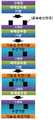
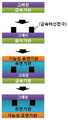
도 1 내지 도 4는 본 발명에 따른 유연투명전극 기판의 제조방법을 각 단계별로 개략적으로 나타낸 도면들이다.1 to 4 are diagrams schematically showing the manufacturing method of the flexible transparent electrode substrate according to the present invention in each step.
본 발명은The present invention
기판상으로 촉매금속층을 증착하는 단계(단계 1);Depositing a catalytic metal layer onto the substrate (step 1);
상기 단계 1의 촉매금속층 상부로 그래핀을 형성하는 단계(단계 2);Forming graphene on the catalytic metal layer of step 1 (step 2);
상기 단계 2에서 형성된 그래핀 상부로 금속 배선을 형성시키는 단계(단계 3);Forming a metal wire on the graphene formed in step 2 (step 3);
상기 단계 3에서 형성된 금속 배선에 유연기판을 형성시키는 단계(단계 4); 및Forming a flexible substrate on the metal wiring formed in the step 3 (step 4); And
상기 단계 1의 기판을 분리한 후, 촉매금속층을 제거하는 단계(단계 5)를 포함하는, 금속배선이 함몰되고 그래핀을 포함하는 유연(flexible) 투명전극 기판의 제조방법을 제공한다.
After separating the substrate of step 1, the step of removing the catalyst metal layer (step 5), the metal wiring is recessed and provides a method for manufacturing a flexible (electrode) transparent electrode substrate comprising a graphene.
이하, 본 발명에 따른 유연투명전극 기판의 제조방법을 각 단계별로 상세히 설명한다.
Hereinafter, the manufacturing method of the flexible transparent electrode substrate according to the present invention will be described in detail for each step.
본 발명에 따른 유연투명전극 기판의 제조방법에 있어서, 단계 1은 기판상으로 촉매금속층을 증착하는 단계이다. 이때, 상기 단계 1의 기판으로는 유리기판, 금속기판, 실리콘 웨이퍼, 세라믹기판 등을 사용할 수 있으나, 이에 제한되는 것은 아니다.In the method of manufacturing a flexible transparent electrode substrate according to the present invention, step 1 is a step of depositing a catalyst metal layer on the substrate. In this case, a glass substrate, a metal substrate, a silicon wafer, a ceramic substrate, and the like may be used as the substrate of step 1, but is not limited thereto.
또한, 상기 단계 1의 촉매금속은 니켈(Ni), 구리(Cu), 루테늄(Ru), 이리듐(Ir), 철(Fe), 백금(Pt), 알루미늄(Al) 등을 사용할 수 있다. 상기 촉매금속층을 증착함으로써 촉매금속층 상부로 그래핀을 형성시킬 수 있으며, 촉매금속층의 두께는 10 내지 300 nm인 것이 바람직하나, 이에 제한되는 것은 아니다.
In addition, the catalyst metal of step 1 may be nickel (Ni), copper (Cu), ruthenium (Ru), iridium (Ir), iron (Fe), platinum (Pt), aluminum (Al) and the like. Graphene may be formed on the catalyst metal layer by depositing the catalyst metal layer, and the thickness of the catalyst metal layer is preferably 10 to 300 nm, but is not limited thereto.
한편, 상기 단계 1의 촉매금속층을 형성시키기 전, 단계 1의 기판 표면은 플라즈마 처리되는 것이 바람직하다. 상기 플라즈마 처리는 차후 단계 1의 기판 제거를 더욱 용이하게 수행하기 위한 것으로, 별도의 제거도구 또는 제거공정 없이 물리적 힘을 가하여 단계 1의 기판을 제거할 수 있다.
Meanwhile, before forming the catalyst metal layer of step 1, the surface of the substrate of step 1 is preferably plasma treated. The plasma treatment is to facilitate the subsequent removal of the substrate of step 1, and may remove the substrate of step 1 by applying a physical force without a separate removal tool or removal process.
본 발명에 따른 유연투명전극 기판의 제조방법에 있어서, 단계 2는 상기 단계 1의 촉매금속층 상부로 그래핀을 형성하는 단계이다.In the method of manufacturing a flexible transparent electrode substrate according to the present invention, step 2 is a step of forming graphene on the catalyst metal layer of the step 1.
그래핀을 형성하는 방법 중 대표적인 제조방법으로는 기계적인 방법, 화학기상증착법(Chemical vapor deposition,CVD) 및 화학적 방법 등이 있으며, 상기 단계 2에서는 화학기상증착법을 통해 그래핀을 형성시킨다. 화학적 기상 증착법은 기체상의 성분들이 화학적으로 반응하여 특정 금속이 증착된 기판표면으로 그래핀 박막을 형성시키는 방법으로서, 화학기상증착법을 통해 비교적 결함이 적은 그래핀을 형성시킬 수 있다. 즉, 단계 2에서는 화학기상증착법을 통해 그래핀을 형성시키기 위해 상기 단계 1에서 형성된 촉매금속층 상부로 그래핀을 형성시키며, 이를 통해 결함이 적은 고품질의 그래핀을 형성시킬 수 있다.
Representative methods of forming graphene include mechanical methods, chemical vapor deposition (CVD), and chemical methods. In step 2, graphene is formed through chemical vapor deposition. Chemical vapor deposition is a method in which gaseous components react chemically to form a graphene thin film on a surface of a substrate on which a specific metal is deposited, and chemical vapor deposition can form relatively few defects. That is, in Step 2, to form graphene through chemical vapor deposition, graphene is formed on the catalyst metal layer formed in Step 1, thereby forming high quality graphene with fewer defects.
본 발명에 따른 유연투명전극 기판의 제조방법에 있어서, 단계 3은 상기 단계 2에서 형성된 그래핀 상부로 금속 배선을 형성시키는 단계이다.In the method of manufacturing a flexible transparent electrode substrate according to the present invention, step 3 is a step of forming a metal wiring on the graphene formed in the step 2.
상기 금속 배선은 은(Ag), 구리(Cu), 알루미늄(Al), 금(Au), 백금(Pt), 니켈(Ni) 등의 금속 또는 이들의 합금, 또는 인듐틴옥사이드(ITO), 인듐징크옥사이드(IZO), 인듐징크틴옥사이드(IZTO), 알루미늄징크옥사이드(AZO), 인듐틴옥사이드-은-인듐틴옥사이드(ITO-Ag-ITO), 인듐징크옥사이드-은-인듐징크옥사이드(IZO-Ag-IZO), 인듐징크틴옥사이드-은-인듐징크틴옥사이드(IZTO-Ag-IZTO), 알루미늄징크옥사이드-은-알루미늄징크옥사이드(AZO-Ag-AZO) 등의 전도성 금속 산화물 1종 이상을 프린팅, 전기도금, 진공증착, 열증착, 스퍼터링, 전자빔 증착 등의 방법으로 기판 상부에 코팅 또는 증착하여 형성될 수 있다.
The metal wiring may be a metal such as silver (Ag), copper (Cu), aluminum (Al), gold (Au), platinum (Pt), nickel (Ni) or an alloy thereof, or indium tin oxide (ITO) or indium. Zinc oxide (IZO), Indium zinc tin oxide (IZTO), Aluminum zinc oxide (AZO), Indium tin oxide-Silver-Indium tin oxide (ITO-Ag-ITO), Indium zinc oxide-Silver-Indium zinc oxide (IZO- Ag-IZO), indium zinc tin oxide-silver-indium zinc tin oxide (IZTO-Ag-IZTO), aluminum zinc oxide-silver-aluminum zinc oxide (AZO-Ag-AZO), and at least one conductive metal oxide It may be formed by coating or depositing on the substrate by a method such as electroplating, vacuum deposition, thermal deposition, sputtering, electron beam deposition.
본 발명에 따른 유연투명전극 기판의 제조방법에 있어서, 단계 4는 상기 단계 3에서 형성된 금속 배선에 유연기판을 형성시키는 단계이다. 상기 유연기판은 상기 단계 3에서 형성된 금속 배선 상부로 경화성 폴리머를 코팅한 후, 경화시킴으로써 형성될 수 있으며, 상기 경화성 폴리머는 폴리에틸렌 테레프탈레이트 (PET), 폴리에틸렌 설폰(PES), 폴리에틸렌 나프탈레이트(PEN), 폴리카보네이트(PC), 폴리메틸메타크릴레이트(PMMA), 폴리이미드 (PI), 에틸렌비닐아세테이트(EVA), 아몰포스폴리에틸렌테레프탈레이트(APET), 폴리프로필렌테레프탈레이트(PPT), 폴리에틸렌테레프탈레이트글리세롤(PETG),폴리사이클로헥실렌디메틸렌테레프탈레이트(PCTG), 변성트리아세틸셀룰로스(TAC), 사이클로올레핀폴리머(COP), 사이클로올레핀코폴리머(COC), 디시클로펜타디엔폴리머(DCPD), 시클로펜타디엔폴리머(CPD), 폴리아릴레이트(PAR), 폴리에테르이미드(PEI), 폴리다이메틸실론세인(PDMS), 실리콘수지, 불소수지, 변성에폭시수지 등을 사용할 수 있다. 상기 경화성 폴리머는 금속 배선 상부로 코팅된 후 열 경화, 자외선 경화, 습기 경화, 마이크로 웨이브 경화(microwave), 적외선(IR) 경화 등 사용되는 고분자의 특성에 맞는 경화방법으로 경화된다. 이때, 상기 코팅은 닥터블레이딩(doctor blading), 바코팅(bar coating), 스핀코팅(spin coating), 딥코팅(dip coating), 마이크로 그라비아 코팅(micro gravure), 임프린팅 (imprinting), 잉크젯 프린팅(injet pringting), 스프레이(spray) 등 용액공정이 가능한 코팅방법으로 수행될 수 있으나, 이에 제한되는 것은 아니다.
In the method of manufacturing a flexible transparent electrode substrate according to the present invention, step 4 is a step of forming a flexible substrate on the metal wiring formed in the step 3. The flexible substrate may be formed by coating a curable polymer on the metal wiring formed in step 3 and then curing the curable polymer, wherein the curable polymer is polyethylene terephthalate (PET), polyethylene sulfone (PES), and polyethylene naphthalate (PEN). , Polycarbonate (PC), polymethyl methacrylate (PMMA), polyimide (PI), ethylene vinyl acetate (EVA), amorphous polyethylene terephthalate (APET), polypropylene terephthalate (PPT), polyethylene terephthalate glycerol (PETG), polycyclohexylenedimethylene terephthalate (PCTG), modified triacetylcellulose (TAC), cycloolefin polymer (COP), cycloolefin copolymer (COC), dicyclopentadiene polymer (DCPD), cyclopenta Diene polymer (CPD), polyarylate (PAR), polyetherimide (PEI), polydimethylsiloncein (PDMS), silicone resin, fluorocarbon resin, modified epoxy Etc. it can not be used. The curable polymer is coated on top of the metal wiring and cured by a curing method suitable for the characteristics of the polymer used, such as thermal curing, ultraviolet curing, moisture curing, microwave curing, and infrared curing. At this time, the coating may be applied by doctor blading, bar coating, spin coating, dip coating, micro gravure, imprinting, inkjet printing but is not limited to, a coating method capable of performing a solution process such as spraying, spraying, and spraying.
본 발명에 따른 유연투명전극 기판의 제조방법에 있어서, 단계 5는 상기 단계 1의 기판을 분리한 후, 촉매금속층을 제거하는 단계이다. 단계 4까지 수행되어, 기판/촉매금속층/그래핀/금속 배선/유연기판의 순으로 적층된 적층체가 제조되고, 단계 5에서 기판을 분리한 후, 촉매금속층을 제거함으로써 그래핀을 포함하는 유연투명전극 기판을 제조할 수 있다. 이때, 상기 단계 5에서 단계 1의 기판을 제거하는 것은 일정한 물리적인 힘을 가하여 수행될 수 있으며, 단계 1의 기판 표면에 플라즈마 처리가 된 경우, 더욱 손쉽게 기판을 제거할 수 있다.In the method of manufacturing a flexible transparent electrode substrate according to the present invention, step 5 is a step of removing the catalyst metal layer after separating the substrate of step 1. Performed up to step 4, a laminate laminated in the order of substrate / catalyst metal layer / graphene / metal wiring / flexible substrate is prepared, and after removing the substrate in step 5, flexible transparent containing graphene by removing the catalyst metal layer An electrode substrate can be manufactured. In this case, removing the substrate of step 1 in step 5 may be performed by applying a constant physical force, and when the plasma treatment is performed on the surface of the substrate of step 1, the substrate may be more easily removed.
한편, 상기 촉매금속층의 제거는 KOH, FeCl3, HCl, HF 등의 에칭용액을 사용하여 수행될 수 있으나, 이에 제한되는 것은 아니다.
On the other hand, the catalyst metal layer may be removed using an etching solution such as KOH, FeCl3 , HCl, HF, but is not limited thereto.
본 발명에 따른 유연투명전극 기판의 제조방법은 유연투명전극 기판의 표면에 기능성 유연기판을 형성시키는 단계를 더 포함할 수 있다.The method of manufacturing a flexible transparent electrode substrate according to the present invention may further include forming a functional flexible substrate on the surface of the flexible transparent electrode substrate.
상기 기능성 유연기판은 폴리머 기판, 종이 기판, 금속 기판 등을 사용할 수 있으며, 상기 금속기판으로는 STS 기판, 알루미늄 기판, 구리기판 등을 이용할 수 있다. 상기 기능성 유연기판의 표면은 자외선 차단막, 파장제어막, 광 집속막, 방오성막 또는 투습/투산소 방지막이 코팅되어, 자외선 차단 기능, 파장 변환 기능, 가시광선 및 적외선 영역 집속 기능(렌즈 기능), 지문 및 스크래치(scratch) 방지 기능, 수분 및 산소 방지 기능 등의 복합효과를 나타낼 수 있다. 또한, 상기 기능성 유연기판 표면은 텍스쳐링(texturing) 처리되어, 특정한 패턴을 나타낼 수 있다.
The functional flexible substrate may be a polymer substrate, a paper substrate, a metal substrate, or the like, and the metal substrate may be an STS substrate, an aluminum substrate, a copper substrate, or the like. The surface of the functional flexible substrate is coated with an ultraviolet blocking film, a wavelength control film, a light focusing film, an antifouling film or a moisture permeable / anti-oxygen film, and includes a UV blocking function, a wavelength conversion function, a visible light and an infrared region focusing function (lens function), A combination effect such as a fingerprint and scratch prevention function, and a moisture and oxygen prevention function can be exhibited. In addition, the functional flexible substrate surface may be textured to exhibit a specific pattern.
또한, 본 발명은In addition,
금속기판상으로 그래핀을 형성하는 단계(단계 1);Forming graphene on a metal substrate (step 1);
상기 단계 1에서 형성된 그래핀 상부로 금속 배선을 형성시키는 단계(단계 2);Forming a metal wire on the graphene formed in step 1 (step 2);
상기 단계 2에서 형성된 금속배선에 유연기판을 형성시키는 단계(단계 3); 및Forming a flexible substrate on the metal wire formed in step 2 (step 3); And
상기 단계 1의 금속기판을 제거하는 단계(단계 4)를 포함하는, 금속배선이 함몰되고 그래핀을 포함하는 유연(flexible) 투명전극 기판의 제조방법을 제공한다.
Provided is a method of manufacturing a flexible transparent electrode substrate including a graphene recessed in metal wiring and including a step (step 4) of removing the metal substrate of step 1.
이하, 본 발명에 따른 유연투명전극 기판의 제조방법을 각 단계별로 상세히 설명한다.
Hereinafter, the manufacturing method of the flexible transparent electrode substrate according to the present invention will be described in detail for each step.
본 발명에 따른 유연투명전극 기판의 제조방법에 있어서, 단계 1은 금속기판상으로 그래핀을 형성하는 단계이다. 그래핀을 형성하는 방법 중 대표적인 제조방법으로는 기계적인 방법, 화학기상증착법(Chemical vapor deposition,CVD) 및 화학적 방법 등이 있으며, 상기 단계 1에서는 화학기상증착법을 통해 그래핀을 형성시킨다. 화학적 기상 증착법은 기체상의 성분들이 화학적으로 반응하여 특정 금속이 증착된 기판표면으로 그래핀 박막을 형성시키는 방법으로서, 화학기상증착법을 통해 비교적 결함이 적은 그래핀을 형성시킬 수 있다.In the method of manufacturing a flexible transparent electrode substrate according to the present invention, step 1 is a step of forming graphene on a metal substrate. Representative methods of forming graphene include mechanical methods, chemical vapor deposition (CVD), and chemical methods. In step 1, graphene is formed through chemical vapor deposition. Chemical vapor deposition is a method in which gaseous components react chemically to form a graphene thin film on a surface of a substrate on which a specific metal is deposited, and chemical vapor deposition can form relatively few defects.
이때, 상기 단계 1의 금속기판은 니켈, 구리, 루테늄, 이리듐, 철, 백금 및 알루미늄으로 이루어진 군으로부터 선택되는 1종 이상의 금속을 포함하는 금속기판인 것이 바람직하다. 화학기상증착법을 통해 그래핀을 형성시키기 위해서는 촉매금속이 필요하다. 그러나, 상기 금속들은 그래핀 형성 시 촉매작용을 수행하는 금속들로써, 상기 금속들을 포함하는 금속기판을 사용함으로써 추가적인 촉매물질 없이도 그래핀을 형성할 수 있다. 즉, 촉매금속을 포함하는 금속재질의 기판을 이용하여 촉매금속층 없이 그래핀을 형성할 수 있다.
At this time, the metal substrate of step 1 is preferably a metal substrate containing at least one metal selected from the group consisting of nickel, copper, ruthenium, iridium, iron, platinum and aluminum. Catalytic metals are needed to form graphene through chemical vapor deposition. However, the metals are metals that catalyze the formation of graphene, and thus, graphene may be formed without additional catalyst material by using a metal substrate including the metals. That is, graphene may be formed without a catalytic metal layer by using a metal substrate including a catalytic metal.
본 발명에 따른 유연투명전극 기판의 제조방법에 있어서, 단계 2는 상기 단계 1에서 형성된 그래핀 상부로 금속 배선을 형성시키는 단계이다.In the method of manufacturing a flexible transparent electrode substrate according to the present invention, step 2 is a step of forming a metal wiring on the graphene formed in the step 1.
상기 금속 배선은 은(Ag), 구리(Cu), 알루미늄(Al), 금(Au), 백금(Pt), 니켈(Ni) 등의 금속 또는 이들의 합금, 또는 인듐틴옥사이드(ITO), 인듐징크옥사이드(IZO), 인듐징크틴옥사이드(IZTO), 알루미늄징크옥사이드(AZO), 인듐틴옥사이드-은-인듐틴옥사이드(ITO-Ag-ITO), 인듐징크옥사이드-은-인듐징크옥사이드(IZO-Ag-IZO), 인듐징크틴옥사이드-은-인듐징크틴옥사이드(IZTO-Ag-IZTO), 알루미늄징크옥사이드-은-알루미늄징크옥사이드(AZO-Ag-AZO) 등의 전도성 금속 산화물 1종 이상을 프린팅, 전기도금, 진공증착, 열증착, 스퍼터링, 전자빔 증착 등의 방법으로 기판 상부에 코팅 또는 증착하여 형성될 수 있다.
The metal wiring may be a metal such as silver (Ag), copper (Cu), aluminum (Al), gold (Au), platinum (Pt), nickel (Ni) or an alloy thereof, or indium tin oxide (ITO) or indium. Zinc oxide (IZO), Indium zinc tin oxide (IZTO), Aluminum zinc oxide (AZO), Indium tin oxide-Silver-Indium tin oxide (ITO-Ag-ITO), Indium zinc oxide-Silver-Indium zinc oxide (IZO- Ag-IZO), indium zinc tin oxide-silver-indium zinc tin oxide (IZTO-Ag-IZTO), aluminum zinc oxide-silver-aluminum zinc oxide (AZO-Ag-AZO), and at least one conductive metal oxide It may be formed by coating or depositing on the substrate by a method such as electroplating, vacuum deposition, thermal deposition, sputtering, electron beam deposition.
본 발명에 따른 유연투명전극 기판의 제조방법에 있어서, 단계 3은 상기 단계 2에서 형성된 금속배선에 유연기판을 형성시키는 단계이다. 상기 유연기판은 상기 단계 2에서 형성된 금속배선에 경화성 폴리머를 코팅한 후, 경화시킴으로써 형성될 수 있으며, 상기 경화성 폴리머는 폴리에틸렌 테레프탈레이트 (PET), 폴리에틸렌 설폰(PES), 폴리에틸렌 나프탈레이트(PEN), 폴리카보네이트(PC), 폴리메틸메타크릴레이트(PMMA), 폴리이미드 (PI), 에틸렌비닐아세테이트(EVA), 아몰포스폴리에틸렌테레프탈레이트(APET), 폴리프로필렌테레프탈레이트(PPT), 폴리에틸렌테레프탈레이트글리세롤(PETG),폴리사이클로헥실렌디메틸렌테레프탈레이트(PCTG), 변성트리아세틸셀룰로스(TAC), 사이클로올레핀폴리머(COP), 사이클로올레핀코폴리머(COC), 디시클로펜타디엔폴리머(DCPD), 시클로펜타디엔폴리머(CPD), 폴리아릴레이트(PAR), 폴리에테르이미드(PEI), 폴리다이메틸실론세인(PDMS), 실리콘수지, 불소수지, 변성에폭시수지 등을 사용할 수 있다. 상기 경화성 폴리머는 금속 배선 상부로 코팅된 후 열 경화, 자외선 경화, 습기 경화, 마이크로 웨이브 경화(microwave), 적외선(IR) 경화 등 사용되는 고분자의 특성에 맞는 경화방법으로 경화된다. 이때, 상기 코팅은 닥터블레이딩(doctor blading), 바코팅(bar coating), 스핀코팅(spin coating), 딥코팅(dip coating), 마이크로 그라비아 코팅(micro gravure), 임프린팅 (imprinting), 잉크젯 프린팅(injet pringting), 스프레이(spray) 등 용액공정이 가능한 코팅방법으로 수행될 수 있으나, 이에 제한되는 것은 아니다.
In the method of manufacturing a flexible transparent electrode substrate according to the present invention, step 3 is a step of forming a flexible substrate on the metal wiring formed in the step 2. The flexible substrate may be formed by coating a curable polymer on the metal wiring formed in step 2 and then curing the curable polymer, wherein the curable polymer is polyethylene terephthalate (PET), polyethylene sulfone (PES), polyethylene naphthalate (PEN), Polycarbonate (PC), Polymethylmethacrylate (PMMA), Polyimide (PI), Ethylene Vinyl Acetate (EVA), Amorphous Polyethylene Terephthalate (APET), Polypropylene Terephthalate (PPT), Polyethylene Terephthalate Glycerol ( PETG), polycyclohexylenedimethylene terephthalate (PCTG), modified triacetylcellulose (TAC), cycloolefin polymer (COP), cycloolefin copolymer (COC), dicyclopentadiene polymer (DCPD), cyclopentadiene Polymer (CPD), Polyarylate (PAR), Polyetherimide (PEI), Polydimethylsiloncene (PDMS), Silicone Resin, Fluorine Resin, Modified Epoxy Resin The can be used. The curable polymer is coated on top of the metal wiring and cured by a curing method suitable for the characteristics of the polymer used, such as thermal curing, ultraviolet curing, moisture curing, microwave curing, and infrared curing. At this time, the coating may be applied by doctor blading, bar coating, spin coating, dip coating, micro gravure, imprinting, inkjet printing but is not limited to, a coating method capable of performing a solution process such as spraying, spraying, and spraying.
본 발명에 따른 유연투명전극 기판의 제조방법에 있어서, 단계 4는 상기 단계 1의 금속기판을 제거하는 단계이다. 단계 3까지 수행되어, 금속기판/그래핀/금속 배선/유연기판의 순으로 적층된 적층체가 제조되고, 단계 4에서 금속기판을 제거함으로써, 그래핀을 포함하는 유연투명전극 기판을 제조할 수 있다. 상기 단계 4에서 단계 1의 금속기판을 제거하는 것은 KOH, FeCl3, HCl, HF 등의 에칭용액을 사용하여 수행될 수 있으나, 이에 제한되는 것은 아니다.
In the method of manufacturing a flexible transparent electrode substrate according to the present invention, step 4 is a step of removing the metal substrate of step 1. By performing the step 3, a laminate laminated in the order of metal substrate / graphene / metal wiring / flexible substrate is manufactured, and by removing the metal substrate in step 4, a flexible transparent electrode substrate including graphene can be manufactured. . Removing the metal substrate of step 1 in step 4 may be performed using an etching solution such as KOH, FeCl3 , HCl, HF, but is not limited thereto.
본 발명에 따른 유연투명전극 기판의 제조방법은 유연투명전극 기판의 표면에 기능성 유연기판을 형성시키는 단계를 더 포함할 수 있다.The method of manufacturing a flexible transparent electrode substrate according to the present invention may further include forming a functional flexible substrate on the surface of the flexible transparent electrode substrate.
상기 기능성 유연기판은 폴리머 기판, 종이 기판, 금속 기판 등을 사용할 수 있으며, 상기 금속기판으로는 STS 기판, 알루미늄 기판, 구리기판 등을 이용할 수 있다. 상기 기능성 유연기판의 표면은 자외선 차단막, 파장제어막, 광 집속막, 방오성막 또는 투습/투산소 방지막이 코팅되어, 자외선 차단 기능, 파장 변환 기능, 가시광선 및 적외선 영역 집속 기능(렌즈 기능), 지문 및 스크래치(scratch) 방지 기능, 수분 및 산소 방지 기능 등의 복합효과를 나타낼 수 있다. 또한, 상기 기능성 유연기판 표면은 텍스쳐링(texturing) 처리되어, 특정한 패턴을 나타낼 수 있다.
The functional flexible substrate may be a polymer substrate, a paper substrate, a metal substrate, or the like, and the metal substrate may be an STS substrate, an aluminum substrate, a copper substrate, or the like. The surface of the functional flexible substrate is coated with an ultraviolet blocking film, a wavelength control film, a light focusing film, an antifouling film or a moisture permeable / anti-oxygen film, and includes a UV blocking function, a wavelength conversion function, a visible light and an infrared region focusing function (lens function), A combination effect such as a fingerprint and scratch prevention function, and a moisture and oxygen prevention function can be exhibited. In addition, the functional flexible substrate surface may be textured to exhibit a specific pattern.
나아가, 본 발명은Further,
기판상으로 박리층을 형성하는 단계(단계 1);Forming a release layer on the substrate (step 1);
상기 단계 1에서 형성된 박리층 상부로 촉매금속층을 형성시키는 단계(단계 2);Forming a catalyst metal layer on the release layer formed in step 1 (step 2);
상기 단계 2에서 형성된 촉매금속층 상부로 그래핀을 형성하는 단계(단계 3);Forming graphene on the catalyst metal layer formed in step 2 (step 3);
상기 단계 3에서 형성된 그래핀 상부로 금속 배선을 형성시키는 단계(단계 4);Forming a metal wire on the graphene formed in step 3 (step 4);
상기 단계 4에서 형성된 금속배선에 유연기판을 형성시키는 단계(단계 5); 및Forming a flexible substrate on the metal wiring formed in step 4 (step 5); And
상기 단계 1의 기판으로부터 박리층을 제거한 후, 촉매금속층을 제거하는 단계(단계 6)를 포함하는 금속배선이 함몰되고 그래핀을 포함하는 유연(flexible) 투명전극 기판의 제조방법을 제공한다.
After removing the exfoliation layer from the substrate of step 1, the metal wiring including the step of removing the catalyst metal layer (step 6) is recessed and provides a method of manufacturing a flexible (electrode) transparent electrode substrate comprising a graphene.
이하, 본 발명에 따른 유연투명전극 기판의 제조방법을 각 단계별로 상세히 설명한다.
Hereinafter, the manufacturing method of the flexible transparent electrode substrate according to the present invention will be described in detail for each step.
본 발명에 따른 유연투명전극 기판의 제조방법에 있어서, 단계 1은 기판상으로 박리층을 형성하는 단계이다. 이때, 상기 단계 1의 기판으로는 유리기판, 금속기판, 실리콘 웨이퍼, 세라믹기판 등을 사용할 수 있으나, 이에 제한되는 것은 아니다.In the method of manufacturing a flexible transparent electrode substrate according to the present invention, step 1 is a step of forming a release layer on the substrate. In this case, a glass substrate, a metal substrate, a silicon wafer, a ceramic substrate, and the like may be used as the substrate of step 1, but is not limited thereto.
단계 1의 상기 박리층은 차후 단계 1의 기판 제거를 더욱 용이하게 수행하기 위한 것으로, 상기 박리층을 추가함으로써 기판으로부터 촉매금속층을 손쉽게 분리해낼 수 있다. 박리층을 형성시켜 기판을 분리하는 경우, 기판이 제거된 분리면의 표면을 더욱 평탄하게 할 수 있고, 물리적인 힘을 가함으로써 손쉽게 단계 1의 기판을 분리할 수 있는 효과가 있어 본 발명에 따른 유연투명전극 기판을 태양전지, 디스플레이 소자와 같은 전자소자에 적용하기 용이하다.The release layer of step 1 is to facilitate the subsequent removal of the substrate of step 1, by adding the release layer can be easily separated from the catalyst metal layer from the substrate. In the case of separating the substrate by forming a release layer, the surface of the separation surface from which the substrate is removed can be made even more smooth, and the substrate can be easily separated by applying a physical force, thereby making it easier to remove the substrate according to the present invention. The flexible transparent electrode substrate can be easily applied to electronic devices such as solar cells and display devices.
이때, 상기 박리층은 실리콘 수지, 불소수지, 다이아몬드 라이크 카본(diamond like carbon, DLC) 및 산화지르코늄 막으로 이루어지는 군으로부터 선택되는 1종 이상의 물질을 이용하여 형성될 수 있으나, 이에 제한되는 것은 아니다.
In this case, the release layer may be formed using one or more materials selected from the group consisting of silicone resins, fluororesins, diamond like carbon (DLC) and zirconium oxide films, but is not limited thereto.
본 발명에 따른 유연투명전극 기판의 제조방법에 있어서, 단계 2는 상기 단계 1에서 형성된 박리층 상부로 촉매금속층을 형성시키는 단계이다.In the method of manufacturing a flexible transparent electrode substrate according to the present invention, step 2 is a step of forming a catalyst metal layer on the release layer formed in step 1.
그래핀을 형성하는 방법 중 대표적인 제조방법으로는 기계적인 방법, 화학기상증착법(Chemical vapor deposition,CVD) 및 화학적 방법 등이 있다. 이때, 화학적 기상 증착법은 기체상의 성분들이 화학적으로 반응하여 특정 금속이 증착된 기판표면으로 그래핀 박막을 형성시키는 방법으로서, 화학기상증착법을 통해 비교적 결함이 적은 그래핀을 형성시킬 수 있다. 이에, 상기 단계 2에서는 화학기상증착법을 통해 그래핀을 형성시키기 위하여, 박리층 상부로 촉매금속층을 형성시킨다.Typical methods of forming graphene include mechanical methods, chemical vapor deposition (CVD), and chemical methods. In this case, the chemical vapor deposition method is a method of forming a graphene thin film on the surface of the substrate on which a specific metal is deposited by chemically reacting the gas phase components, it is possible to form a relatively small graphene through the chemical vapor deposition method. Thus, in step 2, in order to form graphene through chemical vapor deposition, a catalyst metal layer is formed on the release layer.
상기 단계 2의 촉매금속으로는 니켈(Ni), 구리(Cu), 루테늄(Ru), 이리듐(Ir), 철(Fe), 백금(Pt), 알루미늄(Al) 등을 사용할 수 있다. 상기 촉매금속층을 증착함으로써 촉매금속층 상부로 그래핀을 형성시킬 수 있으며, 촉매금속층의 두께는 10 내지 300 nm인 것이 바람직하나, 이에 제한되는 것은 아니다.
Nickel (Ni), copper (Cu), ruthenium (Ru), iridium (Ir), iron (Fe), platinum (Pt), aluminum (Al), etc. may be used as the catalyst metal of step 2. Graphene may be formed on the catalyst metal layer by depositing the catalyst metal layer, and the thickness of the catalyst metal layer is preferably 10 to 300 nm, but is not limited thereto.
본 발명에 따른 유연투명전극 기판의 제조방법에 있어서, 단계 3은 상기 단계 2에서 형성된 촉매금속층 상부로 그래핀을 형성하는 단계이다.In the method of manufacturing a flexible transparent electrode substrate according to the present invention, step 3 is a step of forming graphene on the catalyst metal layer formed in the step 2.
상기 단계 3에서는 상기 단계 2에서 형성된 촉매금속층 상부로 화학기상증착법을 통해 그래핀을 형성시키며, 이를 통해 결함이 적은 고품질의 그래핀을 형성시킬 수 있다.
In step 3, graphene is formed on the catalyst metal layer formed in step 2 by chemical vapor deposition, thereby forming high quality graphene with fewer defects.
본 발명에 따른 유연투명전극 기판의 제조방법에 있어서, 단계 4는 상기 단계 3에서 형성된 그래핀 상부로 금속 배선을 형성시키는 단계이다.In the method of manufacturing a flexible transparent electrode substrate according to the present invention, step 4 is a step of forming a metal wiring on the graphene formed in the step 3.
상기 금속 배선은 은(Ag), 구리(Cu), 알루미늄(Al), 금(Au), 백금(Pt), 니켈(Ni) 등의 금속 또는 이들의 합금, 또는 인듐틴옥사이드(ITO), 인듐징크옥사이드(IZO), 인듐징크틴옥사이드(IZTO), 알루미늄징크옥사이드(AZO), 인듐틴옥사이드-은-인듐틴옥사이드(ITO-Ag-ITO), 인듐징크옥사이드-은-인듐징크옥사이드(IZO-Ag-IZO), 인듐징크틴옥사이드-은-인듐징크틴옥사이드(IZTO-Ag-IZTO), 알루미늄징크옥사이드-은-알루미늄징크옥사이드(AZO-Ag-AZO) 등의 전도성 금속 산화물 1종 이상을 프린팅, 전기도금, 진공증착, 열증착, 스퍼터링, 전자빔 증착 등의 방법으로 기판 상부에 코팅 또는 증착하여 형성될 수 있다.
The metal wiring may be a metal such as silver (Ag), copper (Cu), aluminum (Al), gold (Au), platinum (Pt), nickel (Ni) or an alloy thereof, or indium tin oxide (ITO) or indium. Zinc oxide (IZO), Indium zinc tin oxide (IZTO), Aluminum zinc oxide (AZO), Indium tin oxide-Silver-Indium tin oxide (ITO-Ag-ITO), Indium zinc oxide-Silver-Indium zinc oxide (IZO- Ag-IZO), indium zinc tin oxide-silver-indium zinc tin oxide (IZTO-Ag-IZTO), aluminum zinc oxide-silver-aluminum zinc oxide (AZO-Ag-AZO), and at least one conductive metal oxide It may be formed by coating or depositing on the substrate by a method such as electroplating, vacuum deposition, thermal deposition, sputtering, electron beam deposition.
본 발명에 따른 유연투명전극 기판의 제조방법에 있어서, 단계 5는 상기 단계 4에서 형성된 금속배선에 유연기판을 형성시키는 단계이다. 상기 유연기판은 상기 단계 4에서 형성된 금속배선에 경화성 폴리머를 코팅한 후, 경화시킴으로써 형성될 수 있으며, 상기 경화성 폴리머는 폴리에틸렌 테레프탈레이트 (PET), 폴리에틸렌 설폰(PES), 폴리에틸렌 나프탈레이트(PEN), 폴리카보네이트(PC), 폴리메틸메타크릴레이트(PMMA), 폴리이미드 (PI), 에틸렌비닐아세테이트(EVA), 아몰포스폴리에틸렌테레프탈레이트(APET), 폴리프로필렌테레프탈레이트(PPT), 폴리에틸렌테레프탈레이트글리세롤(PETG),폴리사이클로헥실렌디메틸렌테레프탈레이트(PCTG), 변성트리아세틸셀룰로스(TAC), 사이클로올레핀폴리머(COP), 사이클로올레핀코폴리머(COC), 디시클로펜타디엔폴리머(DCPD), 시클로펜타디엔폴리머(CPD), 폴리아릴레이트(PAR), 폴리에테르이미드(PEI), 폴리다이메틸실론세인(PDMS), 실리콘수지, 불소수지, 변성에폭시수지 등을 사용할 수 있다. 상기 경화성 폴리머는 금속 배선 상부로 코팅된 후 열 경화, 자외선 경화, 습기 경화, 마이크로 웨이브 경화(microwave), 적외선(IR) 경화 등 사용되는 고분자의 특성에 맞는 경화방법으로 경화된다. 이때, 상기 코팅은 닥터블레이딩(doctor blading), 바코팅(bar coating), 스핀코팅(spin coating), 딥코팅(dip coating), 마이크로 그라비아 코팅(micro gravure), 임프린팅 (imprinting), 잉크젯 프린팅(injet pringting), 스프레이(spray) 등 용액공정이 가능한 코팅방법으로 수행될 수 있으나, 이에 제한되는 것은 아니다.
In the method of manufacturing a flexible transparent electrode substrate according to the present invention, step 5 is a step of forming a flexible substrate on the metal wiring formed in the step 4. The flexible substrate may be formed by coating a curable polymer on the metal wire formed in step 4 and then curing the curable polymer, wherein the curable polymer is polyethylene terephthalate (PET), polyethylene sulfone (PES), polyethylene naphthalate (PEN), Polycarbonate (PC), Polymethylmethacrylate (PMMA), Polyimide (PI), Ethylene Vinyl Acetate (EVA), Amorphous Polyethylene Terephthalate (APET), Polypropylene Terephthalate (PPT), Polyethylene Terephthalate Glycerol ( PETG), polycyclohexylenedimethylene terephthalate (PCTG), modified triacetylcellulose (TAC), cycloolefin polymer (COP), cycloolefin copolymer (COC), dicyclopentadiene polymer (DCPD), cyclopentadiene Polymer (CPD), Polyarylate (PAR), Polyetherimide (PEI), Polydimethylsiloncene (PDMS), Silicone Resin, Fluorine Resin, Modified Epoxy Resin The can be used. The curable polymer is coated on top of the metal wiring and cured by a curing method suitable for the characteristics of the polymer used, such as thermal curing, ultraviolet curing, moisture curing, microwave curing, and infrared curing. At this time, the coating may be applied by doctor blading, bar coating, spin coating, dip coating, micro gravure, imprinting, inkjet printing but is not limited to, a coating method capable of performing a solution process such as spraying, spraying, and spraying.
본 발명에 따른 유연투명전극 기판의 제조방법에 있어서, 단계 6은 상기 단계 1의 기판으로부터 박리층을 제거한 후, 촉매금속층을 제거하는 단계이다. 단계 5까지 수행되어, 기판/박리층/촉매금속층/그래핀/금속 배선/유연기판의 순으로 적층된 적층체가 제조되고, 단계 6에서 기판으로부터 촉매금속층을 분리한 후, 촉매금속층을 제거함으로써 그래핀을 포함하는 유연투명전극 기판을 제조할 수 있다.In the method of manufacturing a flexible transparent electrode substrate according to the present invention, step 6 is a step of removing the catalyst metal layer after removing the release layer from the substrate of step 1. Step 5 is carried out to produce a laminate laminated in the order of substrate / peel layer / catalyst metal layer / graphene / metal wiring / flexible substrate, and after separating the catalyst metal layer from the substrate in step 6, the catalyst metal layer is removed. A flexible transparent electrode substrate including a pin can be manufactured.
상기 촉매금속층의 제거는 KOH, FeCl3, HCl, HF 등의 에칭용액을 사용하여 수행될 수 있으나, 이에 제한되는 것은 아니다.
Removal of the catalyst metal layer may be performed using an etching solution such as KOH, FeCl3 , HCl, HF, but is not limited thereto.
본 발명에 따른 유연투명전극 기판의 제조방법은 유연투명전극 기판의 표면에 기능성 유연기판을 형성시키는 단계를 더 포함할 수 있다.The method of manufacturing a flexible transparent electrode substrate according to the present invention may further include forming a functional flexible substrate on the surface of the flexible transparent electrode substrate.
상기 기능성 유연기판은 폴리머 기판, 종이 기판, 금속 기판 등을 사용할 수 있으며, 상기 금속기판으로는 STS 기판, 알루미늄 기판, 구리기판 등을 이용할 수 있다. 상기 기능성 유연기판의 표면은 자외선 차단막, 파장제어막, 광 집속막, 방오성막 또는 투습/투산소 방지막이 코팅되어, 자외선 차단 기능, 파장 변환 기능, 가시광선 및 적외선 영역 집속 기능(렌즈 기능), 지문 및 스크래치(scratch) 방지 기능, 수분 및 산소 방지 기능 등의 복합효과를 나타낼 수 있다. 또한, 상기 기능성 유연기판 표면은 텍스쳐링(texturing) 처리되어, 특정한 패턴을 나타낼 수 있다.
The functional flexible substrate may be a polymer substrate, a paper substrate, a metal substrate, or the like, and the metal substrate may be an STS substrate, an aluminum substrate, a copper substrate, or the like. The surface of the functional flexible substrate is coated with an ultraviolet blocking film, a wavelength control film, a light focusing film, an antifouling film or a moisture permeable / anti-oxygen film, and includes a UV blocking function, a wavelength conversion function, a visible light and an infrared region focusing function (lens function), A combination effect such as a fingerprint and scratch prevention function, and a moisture and oxygen prevention function can be exhibited. In addition, the functional flexible substrate surface may be textured to exhibit a specific pattern.
도 1 내지 4는 본 발명에 따른 상기 제조방법들을 통해 그래핀을 포함하는 유연투명전극 기판을 제조하는 것을 각 단계별로 나타낸 도면들이다. 도 1 내지 4에 나타낸 바와 같이 본 발명에 따른 제조방법들을 통해 유연기판 내부에 함몰된 금속 배선 및 그래핀을 포함하는 유연투명전극 기판을 제조할 수 있으며, 제조된 유연투명전극 기판은 낮은 저항값을 나타낼 수 있고 유연한 특성으로 인하여 다양한 전자소자에 적용할 수 있을 것으로 예상된다.
1 to 4 are diagrams illustrating the steps of manufacturing the flexible transparent electrode substrate including graphene through the manufacturing methods according to the present invention. As shown in Figures 1 to 4 through the manufacturing method according to the present invention it can be produced a flexible transparent electrode substrate including a metal wiring and graphene recessed inside the flexible substrate, the manufactured transparent transparent electrode substrate has a low resistance value It is expected to be applicable to various electronic devices due to the flexible characteristics.
본 발명은 상기 제조방법에 의해 제조되어 그래핀을 포함하는 유연투명전극 기판을 제공한다.The present invention is manufactured by the above method to provide a flexible transparent electrode substrate comprising a graphene.
또한, 본 발명은 상기 유연투명전극 기판을 포함하는 전자소자를 제공한다.
In addition, the present invention provides an electronic device including the flexible transparent electrode substrate.
본 발명에 따른 그래핀을 포함하는 유연투명전극 기판은 종래의 ITO, AZO과 같은 투명전극물질이 유연성을 구비하지 못하여 유연기판에 적용하기 어려웠던 점을 개선하여 유연기판 내부에 함몰된 금속 배선 및 우수한 전기적 특성을 나타내는 그래핀을 포함함으로써, 낮은 저항값 및 유연성(flexibility)을 나타낼 수 있다.The flexible transparent electrode substrate including the graphene according to the present invention improves the difficulty of applying to a flexible substrate because the conventional transparent electrode materials such as ITO and AZO do not have flexibility, and the metal wiring recessed inside the flexible substrate and excellent By including graphene exhibiting electrical properties, low resistance and flexibility can be exhibited.
따라서, 본 발명에 따른 유연투명전극 기판은 최근 주목받고 있는 조명소자, 유연 전자소자 등에 적용할 수 있으며, 특히 유연 태양전지, 유연 디스플레이 소자 등에 적용할 수 있다.
Therefore, the flexible transparent electrode substrate according to the present invention can be applied to lighting devices, flexible electronic devices, and the like, which are recently attracting attention, and in particular, can be applied to flexible solar cells, flexible display devices, and the like.
이하, 본 발명을 실시예를 통해 보다 구체적으로 설명한다. 그러나, 하기 실시예는 본 발명을 설명하기 위한 것일 뿐, 하기 실시예에 의하여 본 발명의 권리범위가 한정되는 것은 아니다.
Hereinafter, the present invention will be described more specifically by way of examples. However, the following examples are intended to illustrate the present invention, but the scope of the present invention is not limited by the following examples.
<실시예 1> 금속배선이 결합된 유연투명전극 기판의 제조 1<Example 1> Fabrication of a flexible transparent electrode substrate combined with a metal wiring 1
단계 1 : 구리 재질의 금속기판 상부에 화학기상증착법을 이용하여 그래핀을 형성하였다. 이때, 상기 그래핀의 형성은 하기 방법을 통해 수행되었다.Step 1: Graphene was formed on the copper metal substrate by chemical vapor deposition. At this time, the formation of the graphene was performed through the following method.
구리 포일(foil)을 화학기상증착장비의 석영관내에 삽입하고, 구리 표면의 산화를 방지하기 위해서 90 mTorr의 압력에서 수소(H2)가 10% 혼합된 아르곤(Ar)가스를 주입하면서 그래핀 성장온도인 1000 ℃ 까지 가열하였다. 성장온도까지 가열한후, 성장온도를 10분간 유지하였으며, 1 torr의 압력에서 600W의 플라즈마를 발생시켰다. 이후, CH4를 약 30분 정도 주입함으로써 그래핀을 형성시켰으며, 상온까지 자연냉각시켰다.
Copper foil is inserted into the quartz tube of chemical vapor deposition equipment, and graphene while injecting argon (Ar) gas containing 10% hydrogen (H2 ) at a pressure of 90 mTorr to prevent oxidation of the copper surface. It heated to 1000 degreeC which is a growth temperature. After heating to the growth temperature, the growth temperature was maintained for 10 minutes, generating a plasma of 600W at a pressure of 1 torr. Then, graphene was formed by injecting CH4 in about 30 minutes, and naturally cooled to room temperature.
단계 2 : 그라비아 오프셋(Gravure Offset) 프린팅 장비를 이용하여 상기 단계 1에서 형성된 그래핀 상부로 Ag 페이스트(silver nano paste DGP, 나노신소재(ANP))를 코팅함으로써 40 μm의 선폭 및 2000 μm의 간격을 가지는 Ag 배선을 형성하였고, 형성된 배선을 200 ℃의 온도인 핫플레이트(hot-plate)에서 1시간 열처리 하였다. 열처리 후 Ag 배선의 두께는 약 1 ~ 2 μm를 나타내었다.
Step 2: The Ag paste (silver nano paste DGP) is coated on top of the graphene formed in Step 1 using a Gravure Offset printing apparatus to obtain a line width of 40 μm and a gap of 2000 μm. Eggplant was formed Ag wiring, the formed wiring was heat-treated for 1 hour in a hot-plate (hot-plate) at a temperature of 200 ℃. After the heat treatment, the thickness of the Ag wiring was about 1 to 2 μm.
단계 3 : 상기 단계 2에서 형성된 Ag 배선 상부로 폴리이미드 (PI)를 닥터블레이딩 (Doctor blading) 방법을 이용하여 일정한 두께를 가지는 액체상태의 막으로 코팅하였으며, 이를 경화시킴으로써 2 ~ 400 μm 두께를 가지는 유연기판을 형성시켰다.
Step 3: The polyimide (PI) was coated on the Ag wiring formed in step 2 with a liquid film having a constant thickness by using a doctor blading method, and cured to obtain a thickness of 2 to 400 μm. Eggplant formed a flexible substrate.
단계 4 : 상기 단계 1의 구리재질의 금속기판을 FeCl3 용액에 침지시켜 제거함으로써 금속배선이 함몰되고 그래핀을 포함하는 유연투명전극 기판을 제조하였다.
Step 4: The copper substrate of step 1 was immersed in a FeCl3 solution to remove the metal wiring, and a flexible transparent electrode substrate including graphene was prepared.
<실시예 2> 금속배선이 결합된 유연투명전극 기판의 제조 2Example 2 Fabrication of a Flexible Transparent Electrode Substrate Combined with Metal Wiring 2
단계 1 : 실리콘 웨이퍼 기판 상부에 200 nm 두께의 니켈금속층을 증착하였다. 이때, 상기 니켈금속층의 증착은 실리콘 웨이퍼 위에 SiO2가 증착된 기판을 사용하여 수행하였으며, DC 마그네트론 스퍼터링을 통해 니켈을 증착시켰다. 스퍼터링 파워는 50~100W로 설정하며, 20 sccm의 아르곤 가스를 주입하며 증착하였다. 증착된 니켈금속층의 두께는 약 50 ~ 300 nm였다.
Step 1: A 200 nm thick nickel metal layer was deposited on the silicon wafer substrate. In this case, the nickel metal layer was deposited using a substrate on which a SiO2 was deposited on a silicon wafer, and nickel was deposited through DC magnetron sputtering. Sputtering power was set to 50 ~ 100W, deposited by injecting 20 sccm of argon gas. The deposited nickel metal layer had a thickness of about 50 to 300 nm.
단계 2 : 상기 단계 1에서 코팅된 니켈금속층 상부로 화학기상증착법을 이용하여 그래핀을 형성하였다. 이때, 상기 그래핀의 형성은 하기 방법을 통해 수행되었다.Step 2: Graphene was formed on the nickel metal layer coated in step 1 by using chemical vapor deposition. At this time, the formation of the graphene was performed through the following method.
니켈금속층이 증착된 기판을 화학기상증착장비의 석영관 내에 삽입하고, 구리 표면의 산화를 방지하기 위해서 90 mTorr의 압력에서 수소(H2)가 10% 혼합된 아르곤(Ar)가스를 주입하면서 그래핀 성장온도인 1000 ℃ 까지 가열하였다. 성장온도까지 가열한후, 성장온도를 10분간 유지하였으며, 1 torr의 압력에서 600W의 플라즈마를 발생시켰다. 이후, CH4를 약 30분 정도 주입함으로써 그래핀을 형성시켰으며, 상온까지 자연냉각시켰다.
The substrate on which the nickel metal layer is deposited is inserted into a quartz tube of a chemical vapor deposition apparatus, and an argon (Ar) gas containing 10% hydrogen (H2 ) is injected at a pressure of 90 mTorr to prevent oxidation of the copper surface. It heated to 1000 degreeC which is fin growth temperature. After heating to the growth temperature, the growth temperature was maintained for 10 minutes, generating a plasma of 600W at a pressure of 1 torr. Then, graphene was formed by injecting CH4 in about 30 minutes, and naturally cooled to room temperature.
단계 3 : 그라비아 오프셋(Gravure Offset) 프린팅 장비를 이용하여 상기 단계 2에서 형성된 그래핀 상부로 Ag 페이스트(silver nano paste DGP, 나노신소재(ANP))를 코팅함으로써 40 μm의 선폭 및 2000 μm의 간격을 가지는 Ag 배선을 형성하였고, 형성된 배선을 200oC의 온도인 핫플레이트(hot-plate)에서 1시간 열처리 하였다. 열처리 후 Ag 배선의 두께는 약 1 ~ 2 μm를 나타내었다.
Step 3: Coating Ag paste (silver nano paste DGP) onto the graphene formed in Step 2 using a Gravure Offset printing apparatus to obtain a line width of 40 μm and a gap of 2000 μm. The eggplants were formed with Ag wiring, and the wirings were heat-treated for 1 hour on a hot plate having a temperature of 200° C. After the heat treatment, the thickness of the Ag wiring was about 1 to 2 μm.
단계 4 : 상기 단계 3에서 형성된 Ag 배선 상부로 폴리이미드 (PI)를 닥터블레이딩 (Doctor blading) 방법을 이용하여 일정한 두께를 가지는 액체상태의 막으로 코팅하였으며, 이를 경화시킴으로써 2 ~ 400 μm 두께를 가지는 유연기판을 형성시켰다.
Step 4: The polyimide (PI) was coated on the Ag wiring formed in Step 3 with a liquid film having a constant thickness using a doctor blading method, and then cured to obtain a thickness of 2 to 400 μm. Eggplant formed a flexible substrate.
단계 5 : 상기 단계 1의 실리콘 웨이퍼 기판으로 물리적인 힘을 가하여 실리콘 웨이퍼기판과 촉매금속층을 분리한 후, 촉매금속층(니켈금속층)을 제거하여 금속배선이 함몰되고 그래핀을 포함하는 유연투명전극 기판을 제조하였다. 이때, 상기 촉매금속층(니켈금속층)의 제거는 FeCl3 에칭용액을 이용하여 수행하였다.
Step 5: After separating the silicon wafer substrate and the catalyst metal layer by applying a physical force to the silicon wafer substrate of step 1, the catalyst metal layer (nickel metal layer) is removed, the metal wiring is recessed and the flexible transparent electrode substrate containing graphene Was prepared. At this time, the catalyst metal layer (nickel metal layer) was removed using a FeCl3 etching solution.
<실시예 3> 금속배선이 결합된 유연투명전극 기판의 제조 3Example 3 Fabrication of a Flexible Transparent Electrode Substrate Combined with Metal Wiring 3
단계 1 : 실리콘 웨이퍼 기판 상에 박리층으로 다이아몬드 라이크 카본(diamond like carbon, DLC) 박막을 화학기상증착법으로 약 10 ~ 200 nm 두께로 증착하였다.
Step 1: A diamond like carbon (DLC) thin film was deposited on the silicon wafer substrate to a thickness of about 10 to 200 nm by chemical vapor deposition.
단계 2 : 상기 단계 1에서 형성된 박리층 상부로 DC 마그네트론 스퍼터링을 이용하여 니켈을 증착시켜 니켈금속층을 형성시켰다. 이때, 스퍼터링 파워는 50~100W로 설정하였으며, 20 sccm의 아르곤 가스를 주입하며 증착을 수행하였다. 증착된 니켈금속층의 두께는 약 50 ~ 300 nm였다.
Step 2: Nickel was deposited on the release layer formed in Step 1 by using DC magnetron sputtering to form a nickel metal layer. At this time, the sputtering power was set to 50 ~ 100W, deposition was performed by injecting 20 sccm of argon gas. The deposited nickel metal layer had a thickness of about 50 to 300 nm.
단계 3 : 상기 단계 2에서 형성된 니켈금속층 상부로 화학기상증착법을 이용하여 그래핀을 형성하였다. 이때, 상기 그래핀의 형성은 하기 방법을 통해 수행되었다.Step 3: Graphene was formed on the nickel metal layer formed in Step 2 by using chemical vapor deposition. At this time, the formation of the graphene was performed through the following method.
니켈금속층이 증착된 기판을 화학기상증착장비의 석영관내에 삽입하고, 구리 표면의 산화를 방지하기 위해서 90 mTorr의 압력에서 수소(H2)가 10% 혼합된 아르곤(Ar)가스를 주입하면서 그래핀 성장온도인 1000 ℃ 까지 가열하였다. 성장온도까지 가열한후, 성장온도를 10분간 유지하였으며, 1 torr의 압력에서 600W의 플라즈마를 발생시켰다. 이후, CH4를 약 30분 정도 주입함으로써 그래핀을 형성시켰으며, 상온까지 자연냉각시켰다.
The substrate on which the nickel metal layer is deposited is inserted into a quartz tube of a chemical vapor deposition apparatus, and an argon (Ar) gas containing 10% of hydrogen (H2 ) is injected at a pressure of 90 mTorr to prevent oxidation of the copper surface. It heated to 1000 degreeC which is fin growth temperature. After heating to the growth temperature, the growth temperature was maintained for 10 minutes, generating a plasma of 600W at a pressure of 1 torr. Then, graphene was formed by injecting CH4 in about 30 minutes, and naturally cooled to room temperature.
단계 4 : 그라비아 오프셋(Gravure Offset) 프린팅 장비를 이용하여 상기 단계 3에서 형성된 그래핀 상부로 Ag 페이스트(silver nano paste DGP, 나노신소재(ANP))를 코팅함으로써 40 μm의 선폭 및 2000 μm의 간격을 가지는 Ag 배선을 형성하였고, 형성된 배선을 200oC의 온도인 핫플레이트(hot-plate)에서 1시간 열처리 하였다. 열처리 후 Ag 배선의 두께는 약 1 ~ 2 μm를 나타내었다.
Step 4: Coating Ag paste (silver nano paste DGP) onto the graphene formed in Step 3 using a Gravure Offset printing apparatus to obtain a line width of 40 μm and a gap of 2000 μm. The eggplants were formed with Ag wiring, and the wirings were heat-treated for 1 hour on a hot plate having a temperature of 200° C. After the heat treatment, the thickness of the Ag wiring was about 1 to 2 μm.
단계 5 : 상기 단계 4에서 형성된 Ag 배선 상부로 폴리이미드 (PI)를 닥터블레이딩 (Doctor blading) 방법을 이용하여 일정한 두께를 가지는 액체상태의 막으로 코팅하였으며, 이를 경화시킴으로써 2 ~ 400 μm 두께를 가지는 유연기판을 형성시켰다.
Step 5: The polyimide (PI) was coated on the Ag wiring formed in Step 4 with a liquid film having a constant thickness using a doctor blading method, and then cured to obtain a thickness of 2 to 400 μm. Eggplant formed a flexible substrate.
단계 6 : 상기 단계 1에서 형성된 박리층으로부터 상기 실리콘 웨이퍼 기판 물리적으로 분리한 후, 니켈금속층을 제거하여 그래핀을 포함하는 유연투명전극 기판을 제조하였다. 이때, 상기 니켈금속층의 제거는 FeCl, 에칭용액을 이용하여 수행하였다.
Step 6: After physically separating the silicon wafer substrate from the release layer formed in step 1, the nickel metal layer was removed to prepare a flexible transparent electrode substrate including graphene. At this time, the nickel metal layer was removed using FeCl, an etching solution.
<실시예 4> 금속배선이 결합된 유연투명전극 기판의 제조 4Example 4 Fabrication of a Flexible Transparent Electrode Substrate Combined with Metal Wiring 4
상기 실시예 2의 단계 1에서 니켈금속층을 코팅 증착하기 전, 실리콘 웨이퍼의 표면을 플라즈마 처리한 것을 제외하고는 상기 실시예 2와 동일하게 수행하여 그래핀을 포함하는 유연투명전극 기판을 제조하였다.
Before the coating deposition of the nickel metal layer in step 1 of Example 2, except that the surface of the silicon wafer was plasma-treated in the same manner as in Example 2 to prepare a flexible transparent electrode substrate including a graphene.
<비교예 1> 유연투명전극 기판의 제조 1Comparative Example 1 Preparation of a Flexible Transparent Electrode Substrate 1
단계 1 : 구리 재질의 금속기판 상부에 화학기상증착법을 이용하여 그래핀을 형성하였으며, 그래핀의 형성은 하기 방법을 통해 수행하였다.Step 1: The graphene was formed on the upper surface of the copper metal substrate by chemical vapor deposition, and the graphene was formed by the following method.
구리 포일(foil)을 화학기상증착장비의 석영관내에 삽입하고, 구리 표면의 산화를 방지하기 위해서 90 mTorr의 압력에서 수소(H2)가 10% 혼합된 아르곤(Ar)가스를 주입하면서 그래핀 성장온도인 1000 ℃ 까지 가열하였다. 성장온도까지 가열한후, 성장온도를 10분간 유지하였으며, 1 torr의 압력에서 600W의 플라즈마를 발생시켰다. 이후, CH4를 약 30분 정도 주입함으로써 그래핀을 형성시켰으며, 상온까지 자연냉각시켰다.
Copper foil is inserted into the quartz tube of chemical vapor deposition equipment, and graphene while injecting argon (Ar) gas containing 10% hydrogen (H2 ) at a pressure of 90 mTorr to prevent oxidation of the copper surface. It heated to 1000 degreeC which is a growth temperature. After heating to the growth temperature, the growth temperature was maintained for 10 minutes, generating a plasma of 600W at a pressure of 1 torr. Then, graphene was formed by injecting CH4 in about 30 minutes, and naturally cooled to room temperature.
단계 2 : 상기 단계 1에서 형성된 그래핀 상부로 폴리이미드 (PI)를 닥터블레이딩 (Doctor blading) 방법을 이용하여 일정한 두께를 가지는 액체상태의 막으로 코팅하였으며, 이를 경화시킴으로써 2 ~ 400 um 두께를 가지는 유연기판을 형성시켰다.
Step 2: The polyimide (PI) was coated on the graphene formed in Step 1 with a liquid film having a constant thickness using a doctor blading method, and then cured to obtain a thickness of 2 to 400 um. Eggplant formed a flexible substrate.
단계 3 : 상기 단계 1의 구리재질의 금속기판을 FeCl3 에칭용액에 침지시켜 제거함으로써 그래핀을 포함하는 유연투명전극 기판을 제조하였다.
Step 3: A flexible transparent electrode substrate including graphene was prepared by immersing and removing the copper substrate of step 1 in FeCl3 etching solution.
<비교예 2> 유연투명전극 기판의 제조 1Comparative Example 2 Fabrication of Flexible Transparent Electrode Substrate 1
단계 1 : 실리콘 웨이퍼 기판 상부에 200 nm 두께의 니켈금속층을 증착하였다. 이때, DC 마그네트론 스퍼터링을 이용하여 니켈을 증착시켜 니켈금속층을 형성시켰으며, 스퍼터링 파워는 50~100W로 설정하였으며, 20 sccm의 아르곤 가스를 주입하며 증착을 수행하였다. 증착된 니켈금속층의 두께는 약 50 ~ 300 nm였다.
Step 1: A 200 nm thick nickel metal layer was deposited on the silicon wafer substrate. At this time, nickel was deposited using DC magnetron sputtering to form a nickel metal layer. The sputtering power was set to 50 to 100 W, and deposition was performed by injecting 20 sccm of argon gas. The deposited nickel metal layer had a thickness of about 50 to 300 nm.
단계 2 : 상기 단계 1에서 코팅된 니켈금속층 상부로 화학기상증착법을 이용하여 그래핀을 형성하였으며, 그래핀의 형성은 하기 방법을 통해 수행하였다.Step 2: The graphene was formed on the nickel metal layer coated in step 1 by chemical vapor deposition, and the graphene was formed by the following method.
니켈금속층이 증착된 기판을 화학기상증착장비의 석영관내에 삽입하고, 구리 표면의 산화를 방지하기 위해서 90 mTorr의 압력에서 수소(H2)가 10% 혼합된 아르곤(Ar)가스를 주입하면서 그래핀 성장온도인 1000 ℃ 까지 가열하였다. 성장온도까지 가열한후, 성장온도를 10분간 유지하였으며, 1 torr의 압력에서 600W의 플라즈마를 발생시켰다. 이후, CH4를 약 30분 정도 주입함으로써 그래핀을 형성시켰으며, 상온까지 자연냉각시켰다.
The substrate on which the nickel metal layer is deposited is inserted into a quartz tube of a chemical vapor deposition apparatus, and an argon (Ar) gas containing 10% of hydrogen (H2 ) is injected at a pressure of 90 mTorr to prevent oxidation of the copper surface. It heated to 1000 degreeC which is fin growth temperature. After heating to the growth temperature, the growth temperature was maintained for 10 minutes, generating a plasma of 600W at a pressure of 1 torr. Then, graphene was formed by injecting CH4 in about 30 minutes, and naturally cooled to room temperature.
단계 3 : 상기 단계 2에서 형성된 그래핀 상부로 폴리이미드 (PI)를 닥터블레이딩 (Doctor blading) 방법을 이용하여 일정한 두께를 가지는 액체상태의 막으로 코팅하였으며, 이를 경화시킴으로써 2 ~ 400 um 두께를 가지는 유연기판을 형성시켰다.
Step 3: The polyimide (PI) was coated on the graphene formed in Step 2 with a liquid film having a constant thickness by using a doctor blading method, and then cured to obtain a thickness of 2 to 400 um. Eggplant formed a flexible substrate.
단계 4 : 상기 단계 1의 실리콘 웨이퍼 기판으로 물리적인 힘을 가하여 실리콘 웨이퍼기판과 촉매금속층을 분리한 후, 촉매금속층(니켈금속층)을 제거하여 그래핀을 포함하는 유연투명전극 기판을 제조하였다. 이때, 상기 니켈금속층의 제거는 FeCl3 에칭용액을 이용하여 수행하였다.
Step 4: After the physical force is applied to the silicon wafer substrate of step 1 to separate the silicon wafer substrate and the catalyst metal layer, the catalyst metal layer (nickel metal layer) is removed to prepare a flexible transparent electrode substrate including graphene. At this time, the removal of the nickel metal layer was performed using a FeCl3 etching solution.
<실험예 1> 투과도 분석Experimental Example 1 Analysis of Permeability
본 발명에 따른 실시예 1 내지 4와 비교예 1 및 2에서 제조된 그래핀을 포함하는 유연투명전극 기판의 투과도를 분석하기 위하여 UV-visible spectrophotometer를 이용하여 투과도를 분석하였고, 그 결과를 하기 표 1에 나타내었다.
In order to analyze the transmittance of the flexible transparent electrode substrate including the graphene prepared in Examples 1 to 4 and Comparative Examples 1 and 2 according to the present invention, the transmittance was analyzed using a UV-visible spectrophotometer. 1 is shown.
표 1에 나타낸 바와 같이, 본 발명에 따른 제조방법으로 금속 배선을 유연기판 내부에 함몰시켜 제조된 실시예 1의 유연투명전극 기판은 비교예 1과 비슷한 수준의 투과도를 보였으며, 또한 금속 배선을 유연기판 내부에 함몰시켜 제조된 실시예 2 내지 4의 유연투명전극 기판은 비교예 2와 비슷한 수준의 투과도를 보였다. 이를 통해, 본 발명에 따른 제조방법으로 금속 배선을 함몰시키더라도 투과도가 저하되는 문제점이 발생하지 않는 것을 확인할 수 있었다.
As shown in Table 1, the flexible transparent electrode substrate of Example 1 prepared by recessing the metal wiring inside the flexible substrate by the manufacturing method according to the present invention showed a level of transmittance similar to that of Comparative Example 1, The flexible transparent electrode substrates of Examples 2 to 4 prepared by recessing in the flexible substrate showed similar levels of transmittance as in Comparative Example 2. Through this, it was confirmed that the problem of lowering the transmittance does not occur even when the metal wiring is recessed by the manufacturing method according to the present invention.
<실험예 2> 면저항 분석Experimental Example 2 Sheet Resistance Analysis
본 발명에 따른 실시예 1 내지 3과 비교예 1 및 2에서 제조된 그래핀을 포함하는 유연투명전극 기판의 면저항을 분석하기 위하여 4 point probe를 이용하여 저항값을 분석하였고, 그 결과를 하기 표 2에 나타내었다.
In order to analyze the sheet resistance of the flexible transparent electrode substrate including the graphene prepared in Examples 1 to 3 and Comparative Examples 1 and 2 according to the present invention, the resistance value was analyzed using a 4 point probe, and the results are shown in the following table. 2 is shown.
표 2에 나타낸 바와 같이, 본 발명에 따른 제조방법으로 금속 배선을 유연기판 내부에 함몰시켜 제조된 실시예 1의 유연투명전극 기판은 비교예 1에서의 유연투명전극 기판보다 면저항이 매우 낮은 것을 알 수 있으며, 또한 금속 배선을 유연기판 내부에 함몰시켜 제조된 실시예 2 내지 4의 유연투명전극 기판은 비교예 2에서의 유연투명전극 기판보다 면저항이 매우 낮음을 알 수 있다. 이를 통해, 본 발명에 따른 제조방법으로 금속 배선을 유연기판 내부에 함몰시킴으로써 저항값을 현저히 낮출 수 있음을 확인하였다.As shown in Table 2, the flexible transparent electrode substrate of Example 1 prepared by recessing the metal wiring inside the flexible substrate by the manufacturing method according to the present invention was found to have a much lower sheet resistance than the flexible transparent electrode substrate of Comparative Example 1 In addition, it can be seen that the flexible transparent electrode substrates of Examples 2 to 4 manufactured by recessing the metal wiring inside the flexible substrate have much lower sheet resistance than the flexible transparent electrode substrate of Comparative Example 2. Through this, it was confirmed that the resistance value can be significantly lowered by recessing the metal wiring inside the flexible substrate by the manufacturing method according to the present invention.
Claims (20)
Translated fromKorean상기 단계 1의 촉매금속층 상부로 그래핀을 형성하는 단계(단계 2);
상기 단계 2에서 형성된 그래핀 상부로 금속 배선을 형성시키는 단계(단계 3);
상기 단계 3에서 형성된 금속 배선에 유연기판을 형성시키는 단계(단계 4); 및
상기 단계 1의 기판을 분리한 후, 촉매금속층을 제거하는 단계(단계 5)를 포함하는, 금속배선이 함몰되고 그래핀을 포함하는 유연(flexible) 투명전극 기판의 제조방법.
Depositing a catalytic metal layer onto the substrate (step 1);
Forming graphene on the catalytic metal layer of step 1 (step 2);
Forming a metal wire on the graphene formed in step 2 (step 3);
Forming a flexible substrate on the metal wiring formed in the step 3 (step 4); And
After separating the substrate of step 1, the step of removing the catalytic metal layer (step 5), the method of manufacturing a flexible transparent electrode substrate comprising a metal wiring is recessed and containing graphene.
상기 단계 1에서 형성된 그래핀 상부로 금속 배선을 형성시키는 단계(단계 2);
상기 단계 2에서 형성된 금속배선에 유연기판을 형성시키는 단계(단계 3); 및
상기 단계 1의 금속기판을 제거하는 단계(단계 4)를 포함하는, 금속배선이 함몰되고 그래핀을 포함하는 유연(flexible) 투명전극 기판의 제조방법.
Forming graphene on a metal substrate (step 1);
Forming a metal wire on the graphene formed in step 1 (step 2);
Forming a flexible substrate on the metal wire formed in step 2 (step 3); And
Including the step (step 4) of removing the metal substrate of step 1, a method for manufacturing a flexible transparent electrode substrate including a graphene recessed metal wiring.
상기 단계 1에서 형성된 박리층 상부로 촉매금속층을 형성시키는 단계(단계 2);
상기 단계 2에서 형성된 촉매금속층 상부로 그래핀을 형성하는 단계(단계 3);
상기 단계 3에서 형성된 그래핀 상부로 금속 배선을 형성시키는 단계(단계 4);
상기 단계 4에서 형성된 금속배선에 유연기판을 형성시키는 단계(단계 5); 및
상기 단계 1의 기판으로부터 박리층을 제거한 후, 촉매금속층을 제거하는 단계(단계 6)를 포함하는, 금속배선이 함몰되고 그래핀을 포함하는 유연(flexible) 투명전극 기판의 제조방법.
Forming a release layer on the substrate (step 1);
Forming a catalyst metal layer on the release layer formed in step 1 (step 2);
Forming graphene on the catalyst metal layer formed in step 2 (step 3);
Forming a metal wire on the graphene formed in step 3 (step 4);
Forming a flexible substrate on the metal wiring formed in step 4 (step 5); And
After removing the exfoliation layer from the substrate of step 1, the step of removing the catalytic metal layer (step 6), the method of manufacturing a flexible transparent electrode substrate including a graphene recessed metal wiring.
The method of claim 2, wherein the metal substrate of step 1 comprises at least one metal selected from the group consisting of nickel, copper, ruthenium, iridium, iron, platinum, and aluminum. .
The method of claim 1 or 3, wherein the catalytic metal layer is made of a flexible transparent electrode substrate characterized in that it comprises at least one metal selected from the group consisting of nickel, copper, ruthenium, iridium, iron, platinum and aluminum. Way.
The method of claim 1, wherein the surface of the substrate of step 1 is subjected to plasma treatment before depositing the catalytic metal layer.
The method of claim 3, wherein the release layer of step 1 comprises one release material selected from the group consisting of silicone resin, fluorocarbon resin, diamond like carbon (DLC) and zirconium oxide film. Method of manufacturing a flexible transparent electrode substrate.
The metal wire of claim 1, wherein the metal wire is silver (Ag), copper (Cu), aluminum (Al), gold (Au), platinum (Pt), nickel (Ni), chromium ( A method for manufacturing a flexible transparent electrode substrate, characterized in that it is formed of one metal selected from the group consisting of Cr), titanium (Ti), and alloys thereof.
The metal wire according to any one of claims 1 to 3, wherein the metal wiring is indium tin oxide (ITO), indium zinc oxide (IZO), indium zinc tin oxide (IZTO), aluminum zinc oxide (AZO), or gallium zinc oxide. (GZO), florin tin oxide (FTO), indium tin oxide-silver-indium tin oxide (ITO-Ag-ITO), indium zinc oxide-silver-indium zinc oxide (IZO-Ag-IZO), indium zinc tin oxide- Flexible transparency characterized in that it is formed of any one or a mixture thereof selected from the group consisting of silver-indium zinc tin oxide (IZTO-Ag-IZTO) and aluminum zinc oxide-silver-aluminum zinc oxide (AZO-Ag-AZO). Method of manufacturing an electrode substrate.
The process according to any one of claims 1 to 3, wherein the metal wiring is selected from the group consisting of inkjet printing, gravure printing, gravure offset, aerosol printing, screen printing, electroplating, vacuum deposition and photolithography processes. Method for producing a flexible transparent electrode substrate, characterized in that formed through.
The method of manufacturing a flexible transparent electrode substrate according to any one of claims 1 to 3, wherein the flexible substrate is a polymer flexible substrate.
The method of claim 11, wherein the polymer is polyethylene terephthalate (PET), polyethylene sulfone (PES), polyethylene naphthalate (PEN), polycarbonate (PC), polymethylmethacrylate (PMMA), polyimide (PI), Ethylene Vinyl Acetate (EVA), Amorphous Polyethylene Terephthalate (APET), Polypropylene Terephthalate (PPT), Polyethylene Terephthalate Glycerol (PETG), Polycyclohexylenedimethylene Terephthalate (PCTG), Modified Triacetyl Cellulose (TAC) ), Cycloolefin polymer (COP), cycloolefin copolymer (COC), dicyclopentadiene polymer (DCPD), cyclopentadiene polymer (CPD), polyarylate (PAR), polyetherimide (PEI), polydie A method for producing a flexible transparent electrode substrate, characterized in that it is selected from the group consisting of methylsiloncene (PDMS), silicone resins, fluorine resins and modified epoxy resins.
The method of manufacturing a flexible transparent electrode substrate according to any one of claims 1 to 3, further comprising forming a functional flexible substrate on the flexible substrate.
The method of claim 13, wherein the functional flexible substrate is a polymer substrate, a paper substrate, or a metal substrate.
15. The method of claim 14, wherein the metal substrate is an STS substrate, an aluminum (Al) substrate, or a copper (Cu) substrate.
The method of claim 13, wherein a surface of the functional flexible substrate is coated with an ultraviolet blocking film, a wavelength control film, a light focusing film, an antifouling film, or a moisture permeable / oxygen resistant film.
The method of claim 13, wherein the surface of the functional flexible substrate is textured.
A flexible transparent electrode substrate prepared by the manufacturing method of any one of claims 1 to 3 comprising graphene.
An electronic device comprising the flexible transparent electrode substrate of claim 18.
Priority Applications (1)
| Application Number | Priority Date | Filing Date | Title |
|---|---|---|---|
| KR1020110107568AKR101221581B1 (en) | 2011-10-20 | 2011-10-20 | Fabrication method of flexible transparent electrode substrate with graphene, and the flexible transparent electrode substrate substrate thereby |
Applications Claiming Priority (1)
| Application Number | Priority Date | Filing Date | Title |
|---|---|---|---|
| KR1020110107568AKR101221581B1 (en) | 2011-10-20 | 2011-10-20 | Fabrication method of flexible transparent electrode substrate with graphene, and the flexible transparent electrode substrate substrate thereby |
Publications (1)
| Publication Number | Publication Date |
|---|---|
| KR101221581B1true KR101221581B1 (en) | 2013-01-14 |
Family
ID=47841719
Family Applications (1)
| Application Number | Title | Priority Date | Filing Date |
|---|---|---|---|
| KR1020110107568AExpired - Fee RelatedKR101221581B1 (en) | 2011-10-20 | 2011-10-20 | Fabrication method of flexible transparent electrode substrate with graphene, and the flexible transparent electrode substrate substrate thereby |
Country Status (1)
| Country | Link |
|---|---|
| KR (1) | KR101221581B1 (en) |
Cited By (16)
| Publication number | Priority date | Publication date | Assignee | Title |
|---|---|---|---|---|
| CN103928295A (en)* | 2013-01-16 | 2014-07-16 | 中国科学院上海微系统与信息技术研究所 | Method for transferring graphene on flexible substrate |
| KR101495239B1 (en)* | 2013-06-17 | 2015-02-25 | 한국기계연구원 | Method for manufacturing flexible substrate with buried conducting trace using modification layer and flexible substrate manufactured thereby |
| JP2016152217A (en)* | 2015-02-19 | 2016-08-22 | 国立研究開発法人産業技術総合研究所 | Organic electroluminescence element |
| WO2016167583A1 (en)* | 2015-04-15 | 2016-10-20 | 엘지전자 주식회사 | Method for doping graphene, method for manufacturing graphene composite electrode, and graphene structure comprising same |
| KR20160122977A (en)* | 2015-04-15 | 2016-10-25 | 엘지전자 주식회사 | Method for manufacturing graphene hybrid electrode |
| WO2016190684A1 (en)* | 2015-05-26 | 2016-12-01 | 서울대학교산학협력단 | Electronic element and manufacturing method therefor |
| US9515144B2 (en) | 2014-09-23 | 2016-12-06 | Samsung Electronics Co., Ltd. | Fin-type graphene device |
| KR101728838B1 (en) | 2015-01-30 | 2017-04-21 | 한국과학기술연구원 | Sensing electrode comprising interconnected diamond nanoflakes and method for manufacturing the same |
| KR101741354B1 (en) | 2016-01-19 | 2017-05-30 | 경희대학교 산학협력단 | Manufacturing method of flexible films |
| WO2017217634A1 (en)* | 2016-06-17 | 2017-12-21 | 전자부품연구원 | Graphene composite electrode and method for manufacturing same |
| KR20170142368A (en)* | 2016-06-17 | 2017-12-28 | 전자부품연구원 | Electrode for electronic device with transparent substrate comprising bus electrode originated from metal catalyst layer for graphene growth and method of manufacturing the same |
| KR20200050816A (en) | 2018-11-02 | 2020-05-12 | 한국전기연구원 | Suspended electrode and manufacturing method thereof |
| WO2020116803A1 (en)* | 2018-12-07 | 2020-06-11 | 서울대학교산학협력단 | Stretchable and flexible wearable thermoelectric element configured to be coolable and heatable |
| KR20200093947A (en)* | 2019-01-29 | 2020-08-06 | 포항공과대학교 산학협력단 | Transparent electrode, manufacturing method of the same and use of the same |
| CN111708450A (en)* | 2020-05-27 | 2020-09-25 | 西华大学 | A wiring structure and preparation method thereof, flexible touch screen structure and electronic device |
| CN114390767A (en)* | 2020-10-16 | 2022-04-22 | 鹏鼎控股(深圳)股份有限公司 | Manufacturing method of transparent circuit board and transparent circuit board |
Citations (4)
| Publication number | Priority date | Publication date | Assignee | Title |
|---|---|---|---|---|
| JP2010087222A (en) | 2008-09-30 | 2010-04-15 | Toppan Printing Co Ltd | Method of manufacturing printed wiring board, and the printed wiring board |
| JP4647954B2 (en) | 2004-08-13 | 2011-03-09 | 新日鐵化学株式会社 | Method for producing laminate for flexible printed wiring board |
| KR20110031863A (en)* | 2009-09-21 | 2011-03-29 | 삼성테크윈 주식회사 | Method for producing graphene, graphene obtained by the production method, conductive thin film containing the graphene, transparent electrode, heat dissipation or heating element |
| KR20110090396A (en)* | 2010-02-03 | 2011-08-10 | 삼성테크윈 주식회사 | Electrode Formation Method of Touch Panel |
- 2011
- 2011-10-20KRKR1020110107568Apatent/KR101221581B1/ennot_activeExpired - Fee Related
Patent Citations (4)
| Publication number | Priority date | Publication date | Assignee | Title |
|---|---|---|---|---|
| JP4647954B2 (en) | 2004-08-13 | 2011-03-09 | 新日鐵化学株式会社 | Method for producing laminate for flexible printed wiring board |
| JP2010087222A (en) | 2008-09-30 | 2010-04-15 | Toppan Printing Co Ltd | Method of manufacturing printed wiring board, and the printed wiring board |
| KR20110031863A (en)* | 2009-09-21 | 2011-03-29 | 삼성테크윈 주식회사 | Method for producing graphene, graphene obtained by the production method, conductive thin film containing the graphene, transparent electrode, heat dissipation or heating element |
| KR20110090396A (en)* | 2010-02-03 | 2011-08-10 | 삼성테크윈 주식회사 | Electrode Formation Method of Touch Panel |
Cited By (25)
| Publication number | Priority date | Publication date | Assignee | Title |
|---|---|---|---|---|
| CN103928295A (en)* | 2013-01-16 | 2014-07-16 | 中国科学院上海微系统与信息技术研究所 | Method for transferring graphene on flexible substrate |
| KR101495239B1 (en)* | 2013-06-17 | 2015-02-25 | 한국기계연구원 | Method for manufacturing flexible substrate with buried conducting trace using modification layer and flexible substrate manufactured thereby |
| US9515144B2 (en) | 2014-09-23 | 2016-12-06 | Samsung Electronics Co., Ltd. | Fin-type graphene device |
| KR101728838B1 (en) | 2015-01-30 | 2017-04-21 | 한국과학기술연구원 | Sensing electrode comprising interconnected diamond nanoflakes and method for manufacturing the same |
| JP2016152217A (en)* | 2015-02-19 | 2016-08-22 | 国立研究開発法人産業技術総合研究所 | Organic electroluminescence element |
| WO2016167583A1 (en)* | 2015-04-15 | 2016-10-20 | 엘지전자 주식회사 | Method for doping graphene, method for manufacturing graphene composite electrode, and graphene structure comprising same |
| KR101706963B1 (en)* | 2015-04-15 | 2017-02-15 | 엘지전자 주식회사 | Method for manufacturing graphene hybrid electrode |
| KR20160122977A (en)* | 2015-04-15 | 2016-10-25 | 엘지전자 주식회사 | Method for manufacturing graphene hybrid electrode |
| US10497893B2 (en) | 2015-04-15 | 2019-12-03 | Lg Electronics Inc. | Method for doping graphene, method for manufacturing graphene composite electrode, and graphene structure comprising same |
| WO2016190684A1 (en)* | 2015-05-26 | 2016-12-01 | 서울대학교산학협력단 | Electronic element and manufacturing method therefor |
| KR20160139086A (en)* | 2015-05-26 | 2016-12-07 | 서울대학교산학협력단 | Electronic device and manufacturing method of the same |
| KR101723568B1 (en)* | 2015-05-26 | 2017-04-07 | 서울대학교산학협력단 | Electronic device and manufacturing method of the same |
| KR101741354B1 (en) | 2016-01-19 | 2017-05-30 | 경희대학교 산학협력단 | Manufacturing method of flexible films |
| WO2017217634A1 (en)* | 2016-06-17 | 2017-12-21 | 전자부품연구원 | Graphene composite electrode and method for manufacturing same |
| KR20170142368A (en)* | 2016-06-17 | 2017-12-28 | 전자부품연구원 | Electrode for electronic device with transparent substrate comprising bus electrode originated from metal catalyst layer for graphene growth and method of manufacturing the same |
| KR102252956B1 (en)* | 2016-06-17 | 2021-05-17 | 한국전자기술연구원 | Electrode for electronic device with transparent substrate comprising bus electrode originated from metal catalyst layer for graphene growth and method of manufacturing the same |
| KR20200050816A (en) | 2018-11-02 | 2020-05-12 | 한국전기연구원 | Suspended electrode and manufacturing method thereof |
| WO2020116803A1 (en)* | 2018-12-07 | 2020-06-11 | 서울대학교산학협력단 | Stretchable and flexible wearable thermoelectric element configured to be coolable and heatable |
| US11839157B2 (en) | 2018-12-07 | 2023-12-05 | Seoul National University R&Db Foundation | Bidirectional stretchable and flexible wearable thermoelectric module |
| KR20200093947A (en)* | 2019-01-29 | 2020-08-06 | 포항공과대학교 산학협력단 | Transparent electrode, manufacturing method of the same and use of the same |
| KR102174902B1 (en)* | 2019-01-29 | 2020-11-05 | 포항공과대학교 산학협력단 | Transparent electrode, manufacturing method of the same and use of the same |
| CN111708450A (en)* | 2020-05-27 | 2020-09-25 | 西华大学 | A wiring structure and preparation method thereof, flexible touch screen structure and electronic device |
| CN111708450B (en)* | 2020-05-27 | 2023-07-28 | 西华大学 | Wiring structure, preparation method thereof, flexible touch screen structure and electronic equipment |
| CN114390767A (en)* | 2020-10-16 | 2022-04-22 | 鹏鼎控股(深圳)股份有限公司 | Manufacturing method of transparent circuit board and transparent circuit board |
| CN114390767B (en)* | 2020-10-16 | 2024-03-15 | 鹏鼎控股(深圳)股份有限公司 | Manufacturing method of transparent circuit board and transparent circuit board |
Similar Documents
| Publication | Publication Date | Title |
|---|---|---|
| KR101221581B1 (en) | Fabrication method of flexible transparent electrode substrate with graphene, and the flexible transparent electrode substrate substrate thereby | |
| KR101161301B1 (en) | Fabrication method of flexible substrate having buried metal electrode using plasma, and the flexible substrate thereby | |
| KR101191865B1 (en) | Fabrication method of flexible substrate having buried metal electrode and the flexible substrate thereby | |
| TW201521984A (en) | Method for manufacturing buried flexible electrode film using thermal lamination transfer | |
| JP2021001112A (en) | Method for fabrication and transfer of graphene | |
| KR101284535B1 (en) | Transferring method of graphene, and graphene transferred flexible substrate thereby | |
| KR101273695B1 (en) | Method for forming graphene pattern and method for manufacturing electronic element having graphene pattern | |
| US20140205763A1 (en) | Growth of graphene films and graphene patterns | |
| JP5739175B2 (en) | Graphene / polymer laminate and use thereof | |
| KR102017251B1 (en) | Method for Preparation of Graphene Thin Film without Transfer Process | |
| TWI526559B (en) | Process for forming carbon film or inorganic material film on substrate by physical vapor deposition | |
| WO2017040469A1 (en) | Methods for transferring graphene films and substrates comprising graphene films | |
| KR101877500B1 (en) | Method for in-situ Preparation of Graphene Thin Film | |
| CN103378222A (en) | Preparation method for inducing graphene by using laser | |
| WO2015060419A1 (en) | Method for producing graphene film | |
| Cabrero-Vilatela et al. | Atomic layer deposited oxide films as protective interface layers for integrated graphene transfer | |
| KR101463227B1 (en) | Apparatus for manufacturing the flexible substrate with buried metal trace | |
| KR101798720B1 (en) | Method for manufacturing graphene using pre-doping and multy-layer graphene manufactured by the same | |
| JP6725122B2 (en) | Method for improving conductivity of graphene sheet and electrode structure using graphene sheet with improved conductivity | |
| JP5756834B2 (en) | Transfer film, method for producing the same, and method for producing transparent conductive laminate | |
| KR20160048546A (en) | Conductive member and method for manufacturing the same | |
| KR101452802B1 (en) | Manufacturing method for electrode materials and transparent electrode using heat treatment plasma processing of raw materials graphene flakes, and transparent electrode and transparent electrode substrate using the same | |
| KR101495239B1 (en) | Method for manufacturing flexible substrate with buried conducting trace using modification layer and flexible substrate manufactured thereby | |
| WO2012144827A2 (en) | Method for manufacturing a flexible substrate having metal wiring embedded therein, and flexible substrate manufactured by the method | |
| CN111508641A (en) | Transparent Conductive Film |
Legal Events
| Date | Code | Title | Description |
|---|---|---|---|
| A201 | Request for examination | ||
| PA0109 | Patent application | St.27 status event code:A-0-1-A10-A12-nap-PA0109 | |
| PA0201 | Request for examination | St.27 status event code:A-1-2-D10-D11-exm-PA0201 | |
| D13-X000 | Search requested | St.27 status event code:A-1-2-D10-D13-srh-X000 | |
| D14-X000 | Search report completed | St.27 status event code:A-1-2-D10-D14-srh-X000 | |
| E902 | Notification of reason for refusal | ||
| PE0902 | Notice of grounds for rejection | St.27 status event code:A-1-2-D10-D21-exm-PE0902 | |
| P11-X000 | Amendment of application requested | St.27 status event code:A-2-2-P10-P11-nap-X000 | |
| P13-X000 | Application amended | St.27 status event code:A-2-2-P10-P13-nap-X000 | |
| E701 | Decision to grant or registration of patent right | ||
| PE0701 | Decision of registration | St.27 status event code:A-1-2-D10-D22-exm-PE0701 | |
| GRNT | Written decision to grant | ||
| PR0701 | Registration of establishment | St.27 status event code:A-2-4-F10-F11-exm-PR0701 | |
| PR1002 | Payment of registration fee | St.27 status event code:A-2-2-U10-U11-oth-PR1002 Fee payment year number:1 | |
| PG1601 | Publication of registration | St.27 status event code:A-4-4-Q10-Q13-nap-PG1601 | |
| FPAY | Annual fee payment | Payment date:20151209 Year of fee payment:4 | |
| PR1001 | Payment of annual fee | St.27 status event code:A-4-4-U10-U11-oth-PR1001 Fee payment year number:4 | |
| FPAY | Annual fee payment | Payment date:20161207 Year of fee payment:5 | |
| PR1001 | Payment of annual fee | St.27 status event code:A-4-4-U10-U11-oth-PR1001 Fee payment year number:5 | |
| P22-X000 | Classification modified | St.27 status event code:A-4-4-P10-P22-nap-X000 | |
| R18-X000 | Changes to party contact information recorded | St.27 status event code:A-5-5-R10-R18-oth-X000 | |
| LAPS | Lapse due to unpaid annual fee | ||
| PC1903 | Unpaid annual fee | St.27 status event code:A-4-4-U10-U13-oth-PC1903 Not in force date:20180108 Payment event data comment text:Termination Category : DEFAULT_OF_REGISTRATION_FEE | |
| PC1903 | Unpaid annual fee | St.27 status event code:N-4-6-H10-H13-oth-PC1903 Ip right cessation event data comment text:Termination Category : DEFAULT_OF_REGISTRATION_FEE Not in force date:20180108 | |
| R18-X000 | Changes to party contact information recorded | St.27 status event code:A-5-5-R10-R18-oth-X000 | |
| P22-X000 | Classification modified | St.27 status event code:A-4-4-P10-P22-nap-X000 |