KR101220480B1 - Method for atomic layer deposition - Google Patents
Method for atomic layer depositionDownload PDFInfo
- Publication number
- KR101220480B1 KR101220480B1KR1020110127638AKR20110127638AKR101220480B1KR 101220480 B1KR101220480 B1KR 101220480B1KR 1020110127638 AKR1020110127638 AKR 1020110127638AKR 20110127638 AKR20110127638 AKR 20110127638AKR 101220480 B1KR101220480 B1KR 101220480B1
- Authority
- KR
- South Korea
- Prior art keywords
- thin film
- reactant
- gas
- substrate
- atomic layer
- Prior art date
- Legal status (The legal status is an assumption and is not a legal conclusion. Google has not performed a legal analysis and makes no representation as to the accuracy of the status listed.)
- Active
Links
- 238000000034methodMethods0.000titleclaimsabstractdescription43
- 238000000231atomic layer depositionMethods0.000titleclaimsdescription37
- 239000010409thin filmSubstances0.000claimsabstractdescription61
- 239000000758substrateSubstances0.000claimsabstractdescription45
- 238000000151depositionMethods0.000claimsabstractdescription39
- 238000006243chemical reactionMethods0.000claimsabstractdescription35
- 230000008021depositionEffects0.000claimsabstractdescription32
- 239000000463materialSubstances0.000claimsabstractdescription14
- 238000000427thin-film depositionMethods0.000claimsabstractdescription8
- 239000000376reactantSubstances0.000claimsdescription63
- 239000007789gasSubstances0.000claimsdescription50
- 238000010926purgeMethods0.000claimsdescription22
- 238000005728strengtheningMethods0.000claimsdescription14
- 239000007788liquidSubstances0.000claimsdescription5
- MYMOFIZGZYHOMD-UHFFFAOYSA-NDioxygenChemical groupO=OMYMOFIZGZYHOMD-UHFFFAOYSA-N0.000claimsdescription3
- UFHFLCQGNIYNRP-UHFFFAOYSA-NHydrogenChemical group[H][H]UFHFLCQGNIYNRP-UHFFFAOYSA-N0.000claimsdescription3
- 229910001882dioxygenInorganic materials0.000claimsdescription3
- 238000011065in-situ storageMethods0.000claimsdescription3
- 230000002378acidificating effectEffects0.000claimsdescription2
- 230000003014reinforcing effectEffects0.000claims1
- 238000000137annealingMethods0.000abstractdescription4
- 230000002787reinforcementEffects0.000abstract1
- QGZKDVFQNNGYKY-UHFFFAOYSA-NAmmoniaChemical compoundNQGZKDVFQNNGYKY-UHFFFAOYSA-N0.000description16
- 238000005260corrosionMethods0.000description7
- 230000007797corrosionEffects0.000description7
- VEXZGXHMUGYJMC-UHFFFAOYSA-NHydrochloric acidChemical compoundClVEXZGXHMUGYJMC-UHFFFAOYSA-N0.000description6
- 229910021529ammoniaInorganic materials0.000description6
- 239000010410layerSubstances0.000description6
- MHAJPDPJQMAIIY-UHFFFAOYSA-NHydrogen peroxideChemical compoundOOMHAJPDPJQMAIIY-UHFFFAOYSA-N0.000description5
- 239000007795chemical reaction productSubstances0.000description5
- 239000002245particleSubstances0.000description5
- 239000000047productSubstances0.000description5
- 238000005229chemical vapour depositionMethods0.000description4
- 239000000126substanceSubstances0.000description3
- XUIMIQQOPSSXEZ-UHFFFAOYSA-NSiliconChemical compound[Si]XUIMIQQOPSSXEZ-UHFFFAOYSA-N0.000description2
- CBWUNQZJGJFJLZ-UHFFFAOYSA-N[Cl].ClChemical compound[Cl].ClCBWUNQZJGJFJLZ-UHFFFAOYSA-N0.000description2
- 235000011114ammonium hydroxideNutrition0.000description2
- 239000011521glassSubstances0.000description2
- 238000005240physical vapour depositionMethods0.000description2
- 239000004065semiconductorSubstances0.000description2
- 229910052710siliconInorganic materials0.000description2
- 239000010703siliconSubstances0.000description2
- XLYOFNOQVPJJNP-UHFFFAOYSA-NwaterSubstancesOXLYOFNOQVPJJNP-UHFFFAOYSA-N0.000description2
- 239000002253acidSubstances0.000description1
- 238000010276constructionMethods0.000description1
- 238000010924continuous productionMethods0.000description1
- 238000005137deposition processMethods0.000description1
- 238000010586diagramMethods0.000description1
- 230000000694effectsEffects0.000description1
- 239000010408filmSubstances0.000description1
- 229910000041hydrogen chlorideInorganic materials0.000description1
- IXCSERBJSXMMFS-UHFFFAOYSA-Nhydrogen chlorideSubstancesCl.ClIXCSERBJSXMMFS-UHFFFAOYSA-N0.000description1
- QOSATHPSBFQAML-UHFFFAOYSA-Nhydrogen peroxide;hydrateChemical compoundO.OOQOSATHPSBFQAML-UHFFFAOYSA-N0.000description1
- 239000012535impuritySubstances0.000description1
- 239000004973liquid crystal related substanceSubstances0.000description1
- 238000012986modificationMethods0.000description1
- 230000004048modificationEffects0.000description1
- 239000002994raw materialSubstances0.000description1
- 239000002356single layerSubstances0.000description1
- 238000004544sputter depositionMethods0.000description1
Images


Classifications
- H—ELECTRICITY
- H01—ELECTRIC ELEMENTS
- H01L—SEMICONDUCTOR DEVICES NOT COVERED BY CLASS H10
- H01L21/00—Processes or apparatus adapted for the manufacture or treatment of semiconductor or solid state devices or of parts thereof
- H01L21/02—Manufacture or treatment of semiconductor devices or of parts thereof
- H01L21/02104—Forming layers
- H01L21/02107—Forming insulating materials on a substrate
- H01L21/02225—Forming insulating materials on a substrate characterised by the process for the formation of the insulating layer
- H01L21/0226—Forming insulating materials on a substrate characterised by the process for the formation of the insulating layer formation by a deposition process
- H01L21/02263—Forming insulating materials on a substrate characterised by the process for the formation of the insulating layer formation by a deposition process deposition from the gas or vapour phase
- H01L21/02271—Forming insulating materials on a substrate characterised by the process for the formation of the insulating layer formation by a deposition process deposition from the gas or vapour phase deposition by decomposition or reaction of gaseous or vapour phase compounds, i.e. chemical vapour deposition
- H01L21/0228—Forming insulating materials on a substrate characterised by the process for the formation of the insulating layer formation by a deposition process deposition from the gas or vapour phase deposition by decomposition or reaction of gaseous or vapour phase compounds, i.e. chemical vapour deposition deposition by cyclic CVD, e.g. ALD, ALE, pulsed CVD
- H—ELECTRICITY
- H01—ELECTRIC ELEMENTS
- H01L—SEMICONDUCTOR DEVICES NOT COVERED BY CLASS H10
- H01L21/00—Processes or apparatus adapted for the manufacture or treatment of semiconductor or solid state devices or of parts thereof
- H01L21/02—Manufacture or treatment of semiconductor devices or of parts thereof
- H01L21/02041—Cleaning
- H01L21/02043—Cleaning before device manufacture, i.e. Begin-Of-Line process
- H01L21/02046—Dry cleaning only
- H—ELECTRICITY
- H01—ELECTRIC ELEMENTS
- H01L—SEMICONDUCTOR DEVICES NOT COVERED BY CLASS H10
- H01L21/00—Processes or apparatus adapted for the manufacture or treatment of semiconductor or solid state devices or of parts thereof
- H01L21/02—Manufacture or treatment of semiconductor devices or of parts thereof
- H01L21/04—Manufacture or treatment of semiconductor devices or of parts thereof the devices having potential barriers, e.g. a PN junction, depletion layer or carrier concentration layer
- H01L21/18—Manufacture or treatment of semiconductor devices or of parts thereof the devices having potential barriers, e.g. a PN junction, depletion layer or carrier concentration layer the devices having semiconductor bodies comprising elements of Group IV of the Periodic Table or AIIIBV compounds with or without impurities, e.g. doping materials
- H01L21/30—Treatment of semiconductor bodies using processes or apparatus not provided for in groups H01L21/20 - H01L21/26
- H01L21/324—Thermal treatment for modifying the properties of semiconductor bodies, e.g. annealing, sintering
Landscapes
- Engineering & Computer Science (AREA)
- Physics & Mathematics (AREA)
- Condensed Matter Physics & Semiconductors (AREA)
- General Physics & Mathematics (AREA)
- Manufacturing & Machinery (AREA)
- Computer Hardware Design (AREA)
- Microelectronics & Electronic Packaging (AREA)
- Power Engineering (AREA)
- Chemical & Material Sciences (AREA)
- Chemical Kinetics & Catalysis (AREA)
- Chemical Vapour Deposition (AREA)
Abstract
Description
Translated fromKorean본 발명은 원자층 증착방법에 관한 것으로, 증착된 박막의 밀도와 내식성을 증가시킬 수 있는 원자층 증착방법을 제공하기 위한 것이다.
The present invention relates to an atomic layer deposition method, to provide an atomic layer deposition method that can increase the density and corrosion resistance of the deposited thin film.
일반적으로, 반도체 기판이나 글라스 등의 기판 상에 소정 두께의 박막을 증착하는 방법으로는 스퍼터링(sputtering)과 같이 물리적인 충돌을 이용하는 물리 기상 증착법(physical vapor deposition, PVD)과, 화학반응을 이용하는 화학 기상 증착법(chemical vapor deposition, CVD) 등이 있다. 최근 반도체 소자의 디자인 룰(design rule)이 급격하게 미세해짐에 따라 미세 패턴의 박막이 요구되고 박막이 형성되는 영역의 단차 또한 매우 커졌다. 이러한 추세로 인해 원자층 두께의 미세 패턴을 매우 균일하게 형성할 수 있을 뿐만 아니라 스텝 커버리지(step coverage)가 우수한 원자층 증착방법(atomic layer deposition, ALD)의 사용이 증대되고 있다.In general, a method of depositing a thin film having a predetermined thickness on a substrate such as a semiconductor substrate or glass includes physical vapor deposition (PVD) using physical collision, such as sputtering, and chemical reaction using a chemical reaction. Chemical vapor deposition (CVD) and the like. Recently, as the design rules of semiconductor devices are drastically fined, thin films of fine patterns are required, and the step height of regions where thin films are formed is also very large. Due to this trend, the use of atomic layer deposition (ALD), which is capable of forming a very uniform pattern of atomic layer thickness very uniformly and has excellent step coverage, has been increasing.
ALD는 기체 분자들 간의 화학반응을 이용한다는 점에 있어서 일반적인 화학 기상 증착방법과 유사하다. 하지만, 통상의 CVD가 다수의 기체 분자들을 동시에 챔버 내로 주입하여 발생된 반응 생성물을 기판에 증착하는 것과 달리, ALD는 하나의 소스 물질을 포함하는 가스를 챔버 내로 주입하여 가열된 기판에 화학흡착시키고 이후 다른 소스 물질을 포함하는 가스를 챔버에 주입함으로써 기판 표면에서 소스 물질 사이의 화학반응에 의한 생성물이 증착된다는 점에서 차이가 있다. 이러한 ALD는 스텝 커버리지 특성이 매우 우수하며 불순물 함유량이 낮은 순수한 박막을 증착하는 것이 가능하다는 장점을 갖고 있어 현재 널리 각광받고 있다.ALD is similar to the general chemical vapor deposition method in that it uses chemical reactions between gas molecules. However, in contrast to conventional CVD in which multiple gas molecules are simultaneously injected into a chamber to deposit the reaction product generated on the substrate, ALD injects a gas containing one source material into the chamber to chemisorb the heated substrate. There is a difference in that a product by chemical reaction between the source materials is deposited on the substrate surface by injecting a gas containing another source material into the chamber. These ALDs are widely attracting attention because they have the advantage of being able to deposit pure thin films having excellent step coverage characteristics and low impurity contents.
그런데, 기존의 ALD에 의해 형성된 박막은 밀도와 내식성이 약해서 박막의 밀도와 내식성을 향상시킬 수 있는 ALD에 대한 연구가 필요하다 할 것이다.
However, the thin film formed by the existing ALD is weak in density and corrosion resistance, it is necessary to study the ALD that can improve the density and corrosion resistance of the thin film.
본 발명의 실시예들에 따르면 원자층 증착공정에서 박막의 밀도와 내식성을 향상시킬 수 있는 원자층 증착방법을 제공하기 위한 것이다.
According to embodiments of the present invention to provide an atomic layer deposition method that can improve the density and corrosion resistance of the thin film in the atomic layer deposition process.
상술한 본 발명의 실시예들에 따른 박막 품질을 향상시킬 수 있는 원자층 증착방법은, 기판에 제1 증착가스와 제2 증착가스를 순차적으로 제공하여 박막을 증착하는 단계 및 상기 박막이 증착된 기판에 상기 박막의 강화를 위한 제1 반응물질 및 제2 반응물질을 순차적으로 제공하여, 상기 제1 및 제2 반응물질이 상기 기판 표면에서 반응함에 따라 상기 박막을 강화시키는 단계를 포함한다. 여기서, 상기 제1 및 제2 반응물질은 서로 반응하여 발열반응이 발생하는 물질들이 사용된다.The atomic layer deposition method for improving the thin film quality according to the embodiments of the present invention described above, the step of depositing a thin film by sequentially providing a first deposition gas and a second deposition gas on the substrate and the thin film is deposited Sequentially providing a first reactant and a second reactant for strengthening the thin film on the substrate, thereby strengthening the thin film as the first and second reactants react on the substrate surface. Here, the first and second reactants are used to react with each other to generate an exothermic reaction.
일 측에 따르면, 상기 제1 반응물질과 상기 제2 반응물질은 산성 물질과 염기성 물질이 각각 사용된다. 또한, 상기 제1 및 제2 반응물질은 액체 또는 기체 중 어느 하나의 상태 물질이 사용된다. 일 예로, 상기 제1 반응물질은 수소 가스이고, 제2 반응물질은 산소 가스가 사용될 수 있다. 또는, 상기 제1 반응물질은 과산화수소(H2O2)이고 상기 제2 반응물질은 암모니아(NH3)일 수 있다. 또는, 상기 제1 반응물질은 염산 또는 염화수소(HCl)이고 상기 제2 반응물질은 암모니아(NH3)일 수 있다.According to one side, the first reactant and the second reactant is an acidic substance and a basic substance, respectively. In addition, the first and second reactants may be used as a state substance of either liquid or gas. For example, the first reactant may be hydrogen gas, and the second reactant may be oxygen gas. Alternatively, the first reactant may be hydrogen peroxide (H 2 O 2) and the second reactant may be ammonia (NH 3). Alternatively, the first reactant may be hydrochloric acid or hydrogen chloride (HCl) and the second reactant may be ammonia (NH 3).
일 측에 따르면, 상기 박막 증착 단계와 상기 박막 강화 단계는 동일 프로세스 챔버 내에서 인시튜(in-situ)로 수행된다.According to one side, the thin film deposition step and the thin film strengthening step is performed in-situ in the same process chamber.
일 측에 따르면, 상기 박막을 강화시키는 단계는, 상기 제1 반응물질을 제공하는 단계, 퍼지가스를 제공하는 단계, 상기 제2 반응물질을 제공하는 단계 및 퍼지가스를 제공하는 단계를 포함하여 구성된다. 또는, 상기 제1 반응물질을 제공하는 단계 및 상기 제2 반응물질을 제공하는 단계를 포함할 수 있다.
According to one side, the step of strengthening the thin film comprises the steps of providing the first reactant, providing a purge gas, providing the second reactant and providing a purge gas do. Alternatively, the method may include providing the first reactant and providing the second reactant.
이상에서 본 바와 같이, 본 발명의 실시예들에 따르면, 원자층 증착공정 중 일정 두께의 박막이 형성되거나 증착이 완료된 후 동일 챔버 내에서 어닐링을 수행함으로써 박막의 밀도 및 내식성을 향상시킬 수 있다.As described above, according to the embodiments of the present invention, the density and the corrosion resistance of the thin film may be improved by performing annealing in the same chamber after the thin film having a predetermined thickness is formed or the deposition is completed in the atomic layer deposition process.
또한, 동일 챔버 내에서 연속 공정으로 어닐링을 수행하므로 공정의 스루풋이 저하되는 것과 생산성 저하를 방지할 수 있다.
In addition, since the annealing is performed in a continuous process in the same chamber, it is possible to prevent a decrease in throughput and a decrease in productivity of the process.
도 1은 본 발명의 일 실시예에 따른 원자층 증착방법을 설명하기 위한 순서도이다.
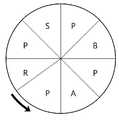
도 2는 본 발명의 일 실시예에 따른 원자층 증착방법을 설명하기 위한 모식도이다.
도 3은 도 2의 변형 실시예에 따른 원자층 증착방법을 설명하기 위한 모식도이다.1 is a flowchart illustrating an atomic layer deposition method according to an embodiment of the present invention.
2 is a schematic view for explaining an atomic layer deposition method according to an embodiment of the present invention.
FIG. 3 is a schematic view illustrating an atomic layer deposition method according to a modified embodiment of FIG. 2.
이하 첨부된 도면들을 참조하여 본 발명의 실시예들을 상세하게 설명하지만, 본 발명이 실시예에 의해 제한되거나 한정되는 것은 아니다. 본 발명을 설명함에 있어서, 공지된 기능 혹은 구성에 대해 구체적인 설명은 본 발명의 요지를 명료하게 하기 위하여 생략될 수 있다.DETAILED DESCRIPTION OF THE PREFERRED EMBODIMENTS Hereinafter, embodiments of the present invention will be described in detail with reference to the accompanying drawings, but the present invention is not limited to or limited by the embodiments. In describing the present invention, a detailed description of well-known functions or constructions may be omitted for clarity of the present invention.
이하, 도 1 내지 도 3을 참조하여 본 발명의 실시예들에 따른 박막 품질 향상이 가능한 원자층 증착방법에 대해서 상세하게 설명한다.Hereinafter, an atomic layer deposition method capable of improving thin film quality according to embodiments of the present invention will be described in detail with reference to FIGS. 1 to 3.
참고적으로, 도 1은 본 발명의 일 실시예에 따른 원자층 증착방법을 설명하기 위한 순서도의 일부이다. 그리고 도 2는 본 발명의 일 실시예에 따른 원자층 증착방법을 설명하기 위한 모식도로써, 증착가스의 제공 순서를 설명하기 위한 도면이다. 도 3은 도 2의 변형 실시예에 따른 원자층 증착방법을 설명하기 위한 모식도이다.For reference, FIG. 1 is a part of a flowchart illustrating an atomic layer deposition method according to an embodiment of the present invention. 2 is a schematic view for explaining an atomic layer deposition method according to an embodiment of the present invention, a diagram for explaining the order of providing the deposition gas. FIG. 3 is a schematic view illustrating an atomic layer deposition method according to a modified embodiment of FIG. 2.
원자층 증착방법은 원자층 증착공정을 이용하여 기판에 소정의 박막을 형성함과 더불어, 상기 형성된 기판 상에 발열 반응이 발생하는 물질을 제공함으로써 형성된 박막의 밀도와 내식성을 향상시키는 어닐링(annealing) 효과를 갖는다.The atomic layer deposition method uses an atomic layer deposition process to form a predetermined thin film on the substrate, and annealing to improve the density and corrosion resistance of the formed thin film by providing a material that generates an exothermic reaction on the formed substrate. Has an effect.
본 실시예에서는 스루풋(throughput)을 향상시키기 위해서 다수(예를 들어, 4장 또는 6장)의 기판에 대해 동시에 증착 공정이 수행되며, 박막의 품질을 확보하기 위해서 각 기판을 수평으로 배치하여 증착이 수행되는 세미 배치 타입(semi-batch type)의 원자층 증착장치를 이용한 원자층 증착방법을 예로 들어 설명한다. 여기서, 세미 배치 타입 원자층 증착장치의 상세한 기술구성은 본 발명의 요지가 아니므로 자세한 설명 및 도시를 생략한다.In this embodiment, a deposition process is performed on a plurality of substrates (for example, four or six sheets) at the same time in order to improve throughput, and in order to ensure the quality of the thin film, the substrates are placed horizontally and deposited. The atomic layer deposition method using the semi-batch type atomic layer deposition apparatus performed will be described as an example. Here, since the detailed technical configuration of the semi-batch type atomic layer deposition apparatus is not the gist of the present invention, detailed description and illustration are omitted.
본 실시예에서 증착 대상이 되는 기판은 실리콘 웨이퍼(silicon wafer)일 수 있다. 그러나 본 발명의 대상이 실리콘 웨이퍼에 한정되는 것은 아니며, 기판은 LCD(liquid crystal display), PDP(plasma display panel)와 같은 평판 디스플레이 장치용으로 사용하는 글라스를 포함하는 투명 기판일 수 있다. 또한, 기판의 형상 및 크기가 도면에 의해 한정되는 것은 아니며, 원형 및 사각형 등 실질적으로 다양한 형상과 크기를 가질 수 있다.In this embodiment, the substrate to be deposited may be a silicon wafer. However, the object of the present invention is not limited to the silicon wafer, and the substrate may be a transparent substrate including glass used for a flat panel display device such as a liquid crystal display (LCD) and a plasma display panel (PDP). In addition, the shape and size of the substrate is not limited by the drawings, and may have substantially various shapes and sizes, such as a circle and a rectangle.
참고적으로 본 발명에서 '제1 증착가스'와 '제2 증착가스'라 함은 서로 기판에 소정 박막을 증착하기 위한 가스들로써, 기판에 증착하고자 하는 박막의 구성 원료 물질을 포함하는 적어도 한 종류 이상의 가스를 말한다. 그리고 '퍼지가스'라 함은 제1 및 제2 증착가스와 화학적으로 반응을 하지 않는 안정한 가스로써, 기판에서 제1 증착가스와 제2 증착가스를 제거하는 역할을 한다. 그리고 '반응물질'이라 함은,//For reference, in the present invention, the 'first deposition gas' and 'second deposition gas' are gases for depositing a predetermined thin film on a substrate, and include at least one kind of a raw material of a thin film to be deposited on a substrate. Say more than gas. The purge gas is a stable gas that does not react chemically with the first and second deposition gases, and serves to remove the first deposition gas and the second deposition gas from the substrate. And "reactant" means //
한편, 원자층 증착공정에서 도 2 또는 도 3에 도시한 바와 같이, 기판에 가스들이 1회씩 제공되면 기판 표면에 단원자층이 증착되는데, 이와 같이 기판에 한 층의 단원자층이 증착되는 것을 1사이클(cycle)이라 한다.On the other hand, as shown in Figure 2 or 3 in the atomic layer deposition process, once the gas is provided to the substrate once, the monoatomic layer is deposited on the surface of the substrate, as described above, a cycle of depositing a single monolayer layer on the substrate It is called a cycle.
한편, 도 2와 도 3에서 부채꼴 형태의 영역들은, 기판에 제1 증착가스가 제공되는 제1 증착영역(S), 퍼지가스가 제공되는 퍼지영역(P), 제2 증착가스가 제공되는 제2 증착영역(R), 그리고 제1 반응물질이 제공되는 제1 반응영역(A)과 제2 반응물질이 제공되는 제2 반응영역(B)이라 한다. 여기서, 도 2와 도 3에서 도시된 영역들은 원자층 증착장치에서 기판이 각각 통과하는 동안 소정의 가스가 제공되는 영역을 말한다.Meanwhile, in FIGS. 2 and 3, the fan-shaped regions may include a first deposition region S in which a first deposition gas is provided on a substrate, a purge region P in which a purge gas is provided, and a second deposition gas in which a second deposition gas is provided. The second deposition region R, and the first reaction region A provided with the first reactant and the second reaction region B provided with the second reactant are provided. Here, the regions shown in FIGS. 2 and 3 refer to regions in which a predetermined gas is provided during the passage of the substrate in the atomic layer deposition apparatus.
도면을 참고하면, 원자층 증착공정이 수행되어 박막이 증착된 후(S11), 상기 박막을 강화시키기 위한 박막 강화 단계(S12)가 수행되며, 이와 같이 박막 증착 단계와 박막 강화 단계가 1사이클이 된다. 여기서, 박막을 강화시키는 단계는 박막을 증착하는 단계와 동일 프로세스 챔버 내부에서 인시튜(in-situ) 공정으로 수행된다.Referring to the drawings, after the atomic layer deposition process is performed to deposit a thin film (S11), the thin film strengthening step (S12) is performed to strengthen the thin film. do. Herein, the step of strengthening the thin film is performed in an in-situ process in the same process chamber as the step of depositing the thin film.
예를 들어, 도 2를 참조하면, 원자층 증착공정은, 기판에 순차적으로 제1 증착가스, 퍼지가스, 제2 증착가스 및 퍼지가스가 제공됨에 따라 기판에 소정의 박막이 단원자층에 해당하는 두께로 증착된다. 다음으로, 상기와 같이 박막이 증착된 기판에 제1 반응물질, 퍼지가스, 제2 반응물질 및 퍼지가스가 제공됨에 따라 박막이 어닐링되어 막질이 강화된다.For example, referring to FIG. 2, in the atomic layer deposition process, as the first deposition gas, the purge gas, the second deposition gas, and the purge gas are sequentially provided to the substrate, a predetermined thin film corresponds to the monoatomic layer. Deposited to thickness. Next, as the first reactant, the purge gas, the second reactant and the purge gas are provided on the substrate on which the thin film is deposited as described above, the thin film is annealed to strengthen the film quality.
상세하게는, 기판이 제1 증착영역(S)을 통과하면 기판 상에 제1 증착가스가 화학흡착되고, 제1 퍼지영역(P)을 통과하는 동안 기판에 흡착되지 않은 잉여 제1 증착가스가 제거된다. 다음으로, 제2 증착영역(R)을 통과하는 동안 제공되는 제2 증착가스가 상술한 단계에서 기판에 화학흡착된 제1 증착가스와 화학적으로 반응함에 따라 반응 생성물이 기판 상에 소정 두께로 증착되어 단원자층에 해당하는 박막이 형성된다. 그리고 제2 퍼지영역(P)을 통과하면서 퍼지가스에 의해 기판에서 잔류 제2 증착가스와 기판에 증착되지 않은 반응 생성물들이 제거된다. 이와 같이 각각 1 번씩의 증착가스가 제공되면 기판에 단원자층의 박막이 형성된다.In detail, when the substrate passes through the first deposition region S, the first deposition gas is chemisorbed on the substrate, and the excess first deposition gas that is not adsorbed onto the substrate is passed through the first purge region P. Removed. Next, as the second deposition gas provided while passing through the second deposition region R chemically reacts with the first deposition gas chemisorbed on the substrate in the above-described step, the reaction product is deposited to a predetermined thickness on the substrate. Thus, a thin film corresponding to the monoatomic layer is formed. The remaining second deposition gas and the reaction products not deposited on the substrate are removed from the substrate by the purge gas while passing through the second purge region P. FIG. When the deposition gas is provided once each, a thin film of monoatomic layer is formed on the substrate.
다음으로, 박막이 증착된 기판이 제1 반응영역(A)을 통과하는 동안 박막 표면에 제1 반응물질이 흡착된다. 마찬가지로 퍼지영역(P)을 통과하면서 상기 박막에 흡착되지 않은 제1 반응물질의 잔류가스 또는 잔류물이 제거된다. 다음으로, 기판이 제2 반응영역(B)을 통과하면 제2 반응물질이 박막 표면에서 제1 반응물질과 화학적으로 반응하면서 열이 발생하고, 이와 같이 발생하는 열이 박막을 어닐링하여 박막의 밀도를 증가시킨다. 마지막으로 퍼지영역(P)에서는 미반응 반응물질들이 제거된다.Next, the first reactant is adsorbed onto the surface of the thin film while the substrate on which the thin film is deposited passes through the first reaction region A. Similarly, while passing through the purge region (P), the residual gas or residue of the first reactant which is not adsorbed to the thin film is removed. Next, when the substrate passes through the second reaction region B, heat is generated while the second reactant chemically reacts with the first reactant on the surface of the thin film, and the heat generated as described above anneals the thin film to give a density of the thin film. To increase. Finally, unreacted reactants are removed from the purge zone P.
여기서, 제1 및 제2 반응물질은 서로 화학적으로 반응하였을 때 열이 발생하는 물질들을 포함한다. 또한, 반응 생성물이 박막에 영향을 미치는 파티클이 발생하지 않는 물질들이 사용된다. 예를 들어, 제1 반응물질은 수소 가스를 포함하고, 제2 반응 가스는 산소 가스를 포함할 수 있다. 그리고 제1 반응물질과 제2 반응물질이 제공되면 기판 표면에서 서로 반응하여 물(H2O)가 생성되는데, 상기와 같은 제1 및 제2 반응물질의 화학반응은 발열반응이므로 열이 발생한다. 그리고 제1 및 제2 반응물질의 반응 후 생성물은 물이기 때문에, 제1 및 제2 반응물질의 화학 반응 후 생성물로 인해 파티클이 발생하지 않아서 박막의 품질을 저하시키는 것을 방지할 수 있다.Here, the first and second reactants include materials that generate heat when chemically reacted with each other. In addition, materials are used which do not generate particles in which the reaction product affects the thin film. For example, the first reactant may include hydrogen gas and the second reactant gas may include oxygen gas. In addition, when the first reactant and the second reactant are provided, water (H 2 O) is generated by reacting with each other on the surface of the substrate. Since the chemical reaction of the first and second reactants is an exothermic reaction, heat is generated. Since the product after the reaction of the first and second reactants is water, particles may not be generated due to the product after the chemical reaction of the first and second reactants, thereby preventing the quality of the thin film.
이외에도 제1 및 제2 반응물질은 서로 반응하여 발열반응이 발생하고, 반응 후 생성물이 파티클이 발생하지 않는 물질이면 실질적으로 다양한 물질들이 사용될 수 있다. 일 예로, 염기성 가스나 액체와 산성 가스나 액체가 사용될 수 있다.In addition, the first and second reactants react with each other to generate an exothermic reaction, and after the reaction, a variety of materials may be used as long as the product does not generate particles. For example, basic gas or liquid and acid gas or liquid may be used.
예를 들어, 제1 반응물질은 과산화수소(H2O2)이고 제2 반응물질은 암모니아(NH3)가 사용될 수 있다. 여기서, 제1 반응물질은 과산화수소 가스 또는 액상의 과산화수소수가 사용되고, 제2 반응물질은 암모니아 가스 또는 액상의 암모니아수가 모두 사용될 수 있다. 이 경우, 제1 및 제2 반응물질인 과산화수소(H2O2)와 암모니아(NH3)의 화학 반응은 발열반응으로, 이러한 발열반응에서 발생하는 열에 의해 기판에 증착된 박막이 어닐링되어 강화된다. 그리고 제1 및 제2 반응물질의 반응 후 생성물은 파티클을 발생시키지 않고 배기가스로 제거된다.For example, the first reactant may be hydrogen peroxide (H 2 O 2) and the second reactant may be ammonia (NH 3). Here, the first reactant may be hydrogen peroxide gas or liquid hydrogen peroxide water, and the second reactant may be both ammonia gas or liquid ammonia water. In this case, the chemical reaction between hydrogen peroxide (H 2 O 2) and ammonia (NH 3), which are the first and second reactants, is an exothermic reaction, and the thin film deposited on the substrate is annealed and strengthened by the heat generated in the exothermic reaction. And after the reaction of the first and second reactants, the product is removed with exhaust gas without generating particles.
또는, 제1 반응물질은 염소(HCl)이고 제2 반응물질은 암모니아(NH3)가 사용될 수 있다. 여기서, 제1 반응물질은 염화수소 가스 또는 염산이 사용될 수 있다. 그리고 제2 반응물질은 암모니아 가스 또는 액상의 암모니아수가 모두 사용될 수 있다. 이 경우에도 제1 및 제2 반응물질인 염소(HCl)와 암모니아(NH3)가 반응하면 발열반응이 발생하고, 반응 생성물은 파티클을 발생시키지 않는다.Alternatively, the first reactant may be chlorine (HCl) and the second reactant may be ammonia (NH 3). Here, hydrogen chloride gas or hydrochloric acid may be used as the first reactant. And the second reactant may be used both ammonia gas or liquid ammonia water. Even in this case, exothermic reaction occurs when chlorine (HCl) and ammonia (NH 3), which are the first and second reactants, react, and the reaction product does not generate particles.
본 실시예에 따르면 박막 강화 단계는, 기판에 증착된 박막 상에 소정의 반응물질을 제공하고, 상기 반응물질이 박막 상에서 서로 반응하여 발생하는 열에 의해 박막의 밀도를 증가되고 내식성이 향상된다.According to the present embodiment, the thin film strengthening step provides a predetermined reactant on the thin film deposited on the substrate, and increases the density of the thin film and improves corrosion resistance by heat generated by the reactants reacting with each other on the thin film.
한편, 상술한 실시예에서는 8분기 원자층 증착공정 상에서 박막 증착 및 박막 강화를 수행하는 것을 예를 들어 설명하였다. 그러나, 제1 및 제2 반응물질을 제공한 후 퍼지시키는 단계를 생략할 수 있다.Meanwhile, in the above-described embodiment, the thin film deposition and the thin film strengthening on the 8th quarter atomic layer deposition process are described as an example. However, purging after providing the first and second reactants may be omitted.
예를 들어, 도 3에 도시한 바와 같이, 제1 증착영역(S), 퍼지영역(P), 제2 증착영역(R), 퍼지영역(P), 제1 반응영역(A) 및 제2 반응영역(B)과 같이 6분기로 구성하는 것도 가능하다. 즉, 제1 반응영역(A)과 제2 반응영역(B) 사이에 퍼지영역을 배치하는 것을 생략할 수 있다. 이 경우, 상술한 실시예와 실질적으로 동일하게 박막 증착 및 박막 강화 단계가 수행된다.For example, as shown in FIG. 3, the first deposition region S, the purge region P, the second deposition region R, the purge region P, the first reaction region A and the second Like the reaction zone (B), it can also be configured in six quarters. That is, disposing a purge zone between the first reaction zone A and the second reaction zone B may be omitted. In this case, the thin film deposition and thin film strengthening steps are performed substantially the same as the above-described embodiment.
또는 도2에 도시한 8분기 원자층 증착공정에서 제1 증착영역(S), 퍼지영역(P), 제2 증착영역(R), 퍼지영역(P), 제1 반응영역(A), 제2 반응영역(B) 및 제1 반응영역(A), 제2 반응영역(B) 순서로 배치되는 것도 가능하다.Alternatively, in the eight-quarter atomic layer deposition process shown in FIG. 2, the first deposition region S, the purge region P, the second deposition region R, the purge region P, the first reaction region A, The second reaction zone B, the first reaction zone A, and the second reaction zone B may be arranged in this order.
한편, 상술한 실시예들에서는 1회의 박막 증착 단계 후에 1회의 박막 강화 단계가 수행되는 것을 예시하였으나, 본 발명이 이에 한정되는 것은 아니며 최종 증착하고자 하는 박막의 두께에 따라 다수의 박막 증착 단계와 다수의 박막 강화 단계를 교번적으로 수행하는 것도 가능하다.Meanwhile, the above-described embodiments illustrate that one thin film strengthening step is performed after one thin film deposition step, but the present invention is not limited thereto, and a plurality of thin film deposition steps and a plurality of thin film deposition steps may be performed according to the thickness of the thin film to be finally deposited. It is also possible to alternately perform the thin film strengthening step of.
이상과 같이 본 발명에서는 구체적인 구성 요소 등과 같은 특정 사항들과 한정된 실시예 및 도면에 의해 설명되었으나 이는 본 발명의 보다 전반적인 이해를 돕기 위해서 제공된 것이다. 또한, 본 발명이 상술한 실시예들에 한정되는 것은 아니며, 본 발명이 속하는 분야에서 통상적인 지식을 가진 자라면 이러한 기재로부터 다양한 수정 및 변형이 가능하다. 그러므로, 본 발명의 사상은 상술한 실시예에 국한되어 정해져서는 아니 되며, 후술하는 특허청구범위뿐 아니라 특허청구범위와 균등하거나 등가적 변형이 있는 모든 것들은 본 발명 사상의 범주에 속한다고 할 것이다.As described above, the present invention has been described by specific embodiments, such as specific components, and limited embodiments and drawings, but this is provided to help a more general understanding of the present invention. In addition, the present invention is not limited to the above-described embodiments, and various modifications and variations are possible to those skilled in the art to which the present invention pertains. Therefore, the spirit of the present invention should not be limited to the above-described embodiments, and all the things that are equivalent to or equivalent to the scope of the claims as well as the claims to be described later belong to the scope of the present invention.
Claims (7)
Translated fromKorean기판에 제1 증착가스와 제2 증착가스를 순차적으로 제공하여 박막을 증착하는 단계; 및
상기 박막이 증착된 기판에 상기 박막의 강화를 위한 제1 반응물질 및 제2 반응물질을 순차적으로 제공하여, 상기 제1 및 제2 반응물질이 상기 기판 표면에서 반응함에 따라 상기 박막을 강화시키는 단계;
를 포함하고,
상기 제1 및 제2 반응물질은 서로 반응하여 발열반응이 발생하는 물질인 원자층 증착방법.
In the atomic layer deposition method,
Depositing a thin film by sequentially providing a first deposition gas and a second deposition gas on a substrate; And
Sequentially providing a first reactant and a second reactant for strengthening the thin film to the substrate on which the thin film is deposited, thereby strengthening the thin film as the first and second reactants react on the surface of the substrate ;
Including,
And the first and second reactants react with each other to generate an exothermic reaction.
상기 제1 반응물질과 상기 제2 반응물질은 산성 물질과 염기성 물질이 각각 사용되는 원자층 증착방법.
The method of claim 1,
The first reactant and the second reactant is an atomic layer deposition method using an acidic material and a basic material, respectively.
상기 제1 및 제2 반응물질은 액체 또는 기체 중 어느 하나의 상태 물질이 사용되는 원자층 증착방법.
The method of claim 2,
The first and second reactants are atomic layer deposition method using a state material of any one of liquid or gas.
상기 제1 반응물질은 수소 가스이고, 제2 반응물질은 산소 가스인 원자층 증착방법.
The method of claim 2,
Wherein the first reactant is hydrogen gas and the second reactant is oxygen gas.
상기 박막 증착 단계와 상기 박막 강화 단계는 동일 프로세스 챔버 내에서 인시튜(in-situ)로 수행되는 원자층 증착방법.
The method of claim 1,
And the thin film deposition step and the thin film strengthening step are performed in-situ in the same process chamber.
상기 박막을 강화시키는 단계는,
상기 제1 반응물질을 제공하는 단계;
퍼지가스를 제공하는 단계;
상기 제2 반응물질을 제공하는 단계; 및
퍼지가스를 제공하는 단계;
를 포함하는 원자층 증착방법.
The method of claim 1,
Reinforcing the thin film,
Providing the first reactant;
Providing a purge gas;
Providing the second reactant; And
Providing a purge gas;
Atomic layer deposition method comprising a.
상기 제1 반응물질을 제공하는 단계; 및
상기 제2 반응물질을 제공하는 단계;
를 포함하는 원자층 증착방법.The method of claim 1,
Providing the first reactant; And
Providing the second reactant;
Atomic layer deposition method comprising a.
Priority Applications (1)
| Application Number | Priority Date | Filing Date | Title |
|---|---|---|---|
| KR1020110127638AKR101220480B1 (en) | 2011-12-01 | 2011-12-01 | Method for atomic layer deposition |
Applications Claiming Priority (1)
| Application Number | Priority Date | Filing Date | Title |
|---|---|---|---|
| KR1020110127638AKR101220480B1 (en) | 2011-12-01 | 2011-12-01 | Method for atomic layer deposition |
Publications (1)
| Publication Number | Publication Date |
|---|---|
| KR101220480B1true KR101220480B1 (en) | 2013-01-21 |
Family
ID=47841545
Family Applications (1)
| Application Number | Title | Priority Date | Filing Date |
|---|---|---|---|
| KR1020110127638AActiveKR101220480B1 (en) | 2011-12-01 | 2011-12-01 | Method for atomic layer deposition |
Country Status (1)
| Country | Link |
|---|---|
| KR (1) | KR101220480B1 (en) |
Citations (4)
| Publication number | Priority date | Publication date | Assignee | Title |
|---|---|---|---|---|
| KR20060003939A (en)* | 2004-07-05 | 2006-01-12 | 삼성전자주식회사 | A film forming method of a semiconductor device and a film forming device of a semiconductor device for performing the same |
| KR20070004780A (en)* | 2004-03-26 | 2007-01-09 | 가부시키가이샤 알박 | Unit layer post-treatment catalytic chemical vapor deposition apparatus and film formation method |
| KR20110045652A (en)* | 2009-10-27 | 2011-05-04 | 주식회사 케이씨텍 | Atomic Layer Deposition Apparatus and Method |
| KR20110087475A (en)* | 2010-01-26 | 2011-08-03 | 서울시립대학교 산학협력단 | Method for forming silicon-based insulator thin film and method for manufacturing thin film transistor substrate using same |
- 2011
- 2011-12-01KRKR1020110127638Apatent/KR101220480B1/enactiveActive
Patent Citations (4)
| Publication number | Priority date | Publication date | Assignee | Title |
|---|---|---|---|---|
| KR20070004780A (en)* | 2004-03-26 | 2007-01-09 | 가부시키가이샤 알박 | Unit layer post-treatment catalytic chemical vapor deposition apparatus and film formation method |
| KR20060003939A (en)* | 2004-07-05 | 2006-01-12 | 삼성전자주식회사 | A film forming method of a semiconductor device and a film forming device of a semiconductor device for performing the same |
| KR20110045652A (en)* | 2009-10-27 | 2011-05-04 | 주식회사 케이씨텍 | Atomic Layer Deposition Apparatus and Method |
| KR20110087475A (en)* | 2010-01-26 | 2011-08-03 | 서울시립대학교 산학협력단 | Method for forming silicon-based insulator thin film and method for manufacturing thin film transistor substrate using same |
Similar Documents
| Publication | Publication Date | Title |
|---|---|---|
| CN1712560B (en) | CVD method using vertical CVD equipment | |
| CN104395987B (en) | Substrate processing apparatus and method | |
| US20070234961A1 (en) | Vertical plasma processing apparatus and method for semiconductor process | |
| KR20100128863A (en) | Atomic Layer Deposition Apparatus and Method | |
| US20050287775A1 (en) | Film formation apparatus and method for semiconductor process | |
| KR20130067123A (en) | Atomic layer deposition method of improving film properties | |
| CN104916569A (en) | Vertical heat treatment apparatus, method of operating vertical heat treatment apparatus, and storage medium | |
| TWI325020B (en) | Deposition methods, and deposition apparatuses | |
| KR20060004976A (en) | Passivation of reactor surface through chemical deactivation | |
| CN105316656A (en) | Film forming apparatus | |
| US10253414B2 (en) | Liquid phase atomic layer deposition | |
| TW202301413A (en) | Apparatus for processing substrate | |
| US20120100308A1 (en) | Ternary metal alloys with tunable stoichiometries | |
| KR100949913B1 (en) | Atomic layer deposition apparatus | |
| KR20180125481A (en) | Plasma electrode and plasma processing device | |
| KR20120098440A (en) | Method of forming titanium nitride film, apparatus for forming titanium nitride film, and storage medium storing program | |
| TW201829828A (en) | TiN TiN-based film and TiN-based film forming method | |
| KR101220480B1 (en) | Method for atomic layer deposition | |
| JP6807275B2 (en) | Film formation method and film deposition equipment | |
| US20230407477A1 (en) | Substrate processing apparatus including improved exhaust structure | |
| KR101163610B1 (en) | Apparatus and method for atomic layer deposition | |
| CN108456872A (en) | Film deposition apparatus | |
| CN105803426B (en) | Use the membrane deposition method and the precipitation equipment of the precipitation equipment with superthin structure | |
| KR101559629B1 (en) | Atomic layer deposition apparatus | |
| JP5803488B2 (en) | Film forming method and film forming apparatus on flexible substrate by atomic layer deposition method |
Legal Events
| Date | Code | Title | Description |
|---|---|---|---|
| A201 | Request for examination | ||
| PA0109 | Patent application | Patent event code:PA01091R01D Comment text:Patent Application Patent event date:20111201 | |
| PA0201 | Request for examination | ||
| E701 | Decision to grant or registration of patent right | ||
| PE0701 | Decision of registration | Patent event code:PE07011S01D Comment text:Decision to Grant Registration Patent event date:20121228 | |
| GRNT | Written decision to grant | ||
| PR0701 | Registration of establishment | Comment text:Registration of Establishment Patent event date:20130103 Patent event code:PR07011E01D | |
| PR1002 | Payment of registration fee | Payment date:20130104 End annual number:3 Start annual number:1 | |
| PG1601 | Publication of registration | ||
| FPAY | Annual fee payment | Payment date:20160104 Year of fee payment:4 | |
| PR1001 | Payment of annual fee | Payment date:20160104 Start annual number:4 End annual number:4 | |
| FPAY | Annual fee payment | Payment date:20170102 Year of fee payment:5 | |
| PR1001 | Payment of annual fee | Payment date:20170102 Start annual number:5 End annual number:5 | |
| FPAY | Annual fee payment | Payment date:20180103 Year of fee payment:6 | |
| PR1001 | Payment of annual fee | Payment date:20180103 Start annual number:6 End annual number:6 | |
| FPAY | Annual fee payment | Payment date:20190103 Year of fee payment:7 | |
| PR1001 | Payment of annual fee | Payment date:20190103 Start annual number:7 End annual number:7 | |
| FPAY | Annual fee payment | Payment date:20200102 Year of fee payment:8 | |
| PR1001 | Payment of annual fee | Payment date:20200102 Start annual number:8 End annual number:8 | |
| PR1001 | Payment of annual fee | Payment date:20210104 Start annual number:9 End annual number:9 | |
| PR1001 | Payment of annual fee | Payment date:20220103 Start annual number:10 End annual number:10 | |
| PR1001 | Payment of annual fee | Payment date:20231226 Start annual number:12 End annual number:12 | |
| PR1001 | Payment of annual fee | Payment date:20241226 Start annual number:13 End annual number:13 |