KR101220464B1 - Express interface apparatus using optical connection - Google Patents
Express interface apparatus using optical connectionDownload PDFInfo
- Publication number
- KR101220464B1 KR101220464B1KR1020090110105AKR20090110105AKR101220464B1KR 101220464 B1KR101220464 B1KR 101220464B1KR 1020090110105 AKR1020090110105 AKR 1020090110105AKR 20090110105 AKR20090110105 AKR 20090110105AKR 101220464 B1KR101220464 B1KR 101220464B1
- Authority
- KR
- South Korea
- Prior art keywords
- optical
- signal
- module
- electrical
- external device
- Prior art date
- Legal status (The legal status is an assumption and is not a legal conclusion. Google has not performed a legal analysis and makes no representation as to the accuracy of the status listed.)
- Expired - Fee Related
Links
Images


Classifications
- G—PHYSICS
- G06—COMPUTING OR CALCULATING; COUNTING
- G06F—ELECTRIC DIGITAL DATA PROCESSING
- G06F13/00—Interconnection of, or transfer of information or other signals between, memories, input/output devices or central processing units
- G06F13/14—Handling requests for interconnection or transfer
- H—ELECTRICITY
- H04—ELECTRIC COMMUNICATION TECHNIQUE
- H04B—TRANSMISSION
- H04B10/00—Transmission systems employing electromagnetic waves other than radio-waves, e.g. infrared, visible or ultraviolet light, or employing corpuscular radiation, e.g. quantum communication
- H04B10/80—Optical aspects relating to the use of optical transmission for specific applications, not provided for in groups H04B10/03 - H04B10/70, e.g. optical power feeding or optical transmission through water
- H04B10/801—Optical aspects relating to the use of optical transmission for specific applications, not provided for in groups H04B10/03 - H04B10/70, e.g. optical power feeding or optical transmission through water using optical interconnects, e.g. light coupled isolators, circuit board interconnections
- G—PHYSICS
- G06—COMPUTING OR CALCULATING; COUNTING
- G06F—ELECTRIC DIGITAL DATA PROCESSING
- G06F13/00—Interconnection of, or transfer of information or other signals between, memories, input/output devices or central processing units
- G06F13/38—Information transfer, e.g. on bus
- G06F13/40—Bus structure
Landscapes
- Engineering & Computer Science (AREA)
- Physics & Mathematics (AREA)
- Theoretical Computer Science (AREA)
- General Engineering & Computer Science (AREA)
- Electromagnetism (AREA)
- Computer Networks & Wireless Communication (AREA)
- Signal Processing (AREA)
- General Physics & Mathematics (AREA)
- Computer Hardware Design (AREA)
- Information Transfer Systems (AREA)
- Optical Couplings Of Light Guides (AREA)
Abstract
Translated fromKorean
Description
Translated fromKorean본 발명은 고속 인터페이스 장치에 관한 것으로, 보다 상세하게는 고속의 신호처리를 지원하는 PCIE(Peripheral Component Interconnect Express)와 광 신호 전송을 지원하는 외부장치간의 고속의 데이터 송수신을 위하여 광/전 변환 및 신호처리 등을 수행함으로써, 고속의 데이터 전송에서 왜곡현상이나 병목현상 없이 신호를 송수신할 수 있도록 한 광 연결을 이용한 고속 인터페이스 장치에 관한 것이다.The present invention relates to a high speed interface device, and more particularly, optical / electric conversion and signal for high speed data transmission and reception between a peripheral component interconnect express (PCIE) supporting high speed signal processing and an external device supporting optical signal transmission. The present invention relates to a high speed interface apparatus using an optical connection capable of transmitting and receiving signals without distortion or bottleneck in high speed data transmission.
일반적으로, 범용 직렬 버스(Universal Serial Bus, 이하 'USB'라 함)는 유니버셜 직렬 버스로서, 종래의 일반적인 직렬 포트를 대체하는 차세대 인터페이스의 규약이며, 컴퓨터 시스템과 키보드, 마우스, 모니터, 모뎀, 프린터 등의 주변기기를 연결하는 외부 버스라고 할 수 있다.In general, the universal serial bus (hereinafter referred to as "USB") is a universal serial bus, and is a protocol of next generation interface that replaces a conventional serial port. It is a computer system, a keyboard, a mouse, a monitor, a modem, and a printer. It can be said to be an external bus connecting peripherals.
이러한 USB 방식으로 데이터를 송수신하기 위해서 사용되는 USB 커넥터는 컴 퓨터 시스템에 결합되는 A-타입 플러그와, 주변기기에 결합되는 미니타입 플러그가 케이블에 의해 연결되어 형성되는 것이 보편적인 것으로, 컴퓨터와 주변기기와의 접속을 위해서 뿐만 아니라, 휴대폰, 휴대용 컴퓨터, 팜PC, PDA, 전자수첩 등의 휴대용 전자장치들과 컴퓨터 시스템과의 상호 데이터 공유를 위해서도 사용된다.The USB connector used to transmit and receive data using the USB method is generally formed by connecting an A-type plug to a computer system and a mini-type plug to a peripheral device by a cable. It is used not only for connection, but also for mutual data sharing with portable electronic devices such as mobile phones, portable computers, palm PCs, PDAs, electronic notebooks, and computer systems.
최근에는, MP3 플레이어나 충전카드, 디지탈 카메라폰 또는 휴대용 메모리 저장장치가 널리 사용되고 있으며, 이러한 휴대용 전자장치와 컴퓨터 시스템과의 결합을 위한 블루터스용 USB 커넥터는, 케이블 대신 A-타입 플러그와 미니타입 플러그의 연결을 위해 일반 PCB(Printed Circuit Board)나 플렉시블 PCB를 사용하고 있다.Recently, MP3 players, charging cards, digital camera phones or portable memory storage devices are widely used, and the Bluetooth connectors for combining these portable electronics with computer systems are A-type plugs and mini-types instead of cables. To connect the plug, a general PCB (Printed Circuit Board) or flexible PCB is used.
따라서, 사용자는 상기 기기들에 장착된 USB 커넥터를 바로 개인용 PC나 기타의 PC에 구비되어 있는 USB 포트에 꽂아 노래를 다운 받거나 또는 기타의 자료를 다운 받아 사용하고 있으며, 별도의 케이블 없이 바로 연결이 가능하여 사용성이 매우 편리한 장점을 가지고 있다.Therefore, the user can directly download a song or other data by plugging the USB connector of the device directly into a USB port provided in a personal PC or other PC, and the connection is made without a separate cable. It has the advantage of being very convenient to use.
그러나, 저장용량과 인터넷 속도가 G(기가)세대에 진입함과 더불어, PC와 주변장치의 데이터 연결은 더 높은 전송속도를 요구하고 있기 때문에, USB 2.0은 날로 높아 가는 접근 속도의 요구를 만족시키지 못하고 있는 바, PC와 주변장치의 데이터 연결에 새로운 인터페이스 규격을 사용하는 것이 절실히 요구되고 있다.However, as storage and Internet speeds enter G (Giga) generations, data connections between PCs and peripherals require higher transfer rates, so USB 2.0 does not meet the demand for ever-increasing access speeds. As a result, there is an urgent need to use new interface specifications for data connections between PCs and peripherals.
하나의 해결방안으로서 eSATA(e Serial Advanced Technology Attachment) 인터페이스를 이용하여 SATA 인터페이스를 컴퓨터 케이스로부터 인출하는 것이 있다. 이러한 인터페이스는 3Gb/S의 대역폭을 지원할 수 있다. 그러나, 전원 신호를 제공 하지 않기 때문에 장치에 전력을 공급할 수 없고, 또한 간단한 기억장치만을 지원하기 때문에 다수의 소비형 전자제품이 이러한 인터페이스를 이용하여 컴퓨터와 연결할 수 없다. 또한 상기 방안은 종래의 많은 USB 장치와도 호환성이 없는 단점을 가지고 있다.One solution is to extract the SATA interface from the computer case using the e Serial Advanced Technology Attachment (eSATA) interface. These interfaces can support 3Gb / S bandwidth. However, because it does not provide a power signal, it cannot power the device, and because it supports only simple storage devices, many consumer electronics cannot connect to a computer using this interface. In addition, the above method has a disadvantage that is incompatible with many conventional USB devices.
한편, 일반적인 컴퓨터 시스템은 대표적인 입/출력 버스로서 PCI(Peripheral Component Interconnect) 버스를 사용하고 있으며, 최근에는 PCI 버스를 대체할 새로운 PCI Express(이하 'PCIE'라 함)가 대두되고 있다.In general, a typical computer system uses a Peripheral Component Interconnect (PCI) bus as a representative input / output bus, and recently, a new PCI Express (hereinafter referred to as 'PCIE') has been introduced to replace the PCI bus.
상기 PCIE는 포인트 투 포인트 연결(Point to Point Connection) 접속을 지원하는 시리얼 버스로써, 수신측과 송신측을 정리한 인터페이스로서의 최소 구성을 x1이라고 정의되며, 어플리케이션의 요구에 따라 x2, x4, x8, x16, x32로 구성되어, 이를 이용해 대역폭을 확장할 수가 있는 가변 대역폭(Scalable Band Width)을 제공한다.The PCIE is a serial bus that supports a point-to-point connection, and the minimum configuration as an interface that combines the receiving side and the transmitting side is defined as x1, and x2, x4, x8, Composed of x16 and x32, it provides scalable bandwidth, which can be used to expand the bandwidth.
현재, 데스크탑용 범용 입/출력(I/O) 슬롯에는 x1이, 그래픽용으로는 x16 구성을 각각 이용하도록 되어 있다. 더불어, PCIE는 포인트 투 포인트 연결, 가변 대역폭(Scalable Band Width), 낮은 전압 차별 신호(Low Voltage Differential Signaling) 등을 특징으로 하고 있으며, 앞으로 데스크 탑 PC 및 노트북 PC뿐만 아니라 서버 영역까지 응용될 수 있다.Currently, x1 is used for the universal input / output (I / O) slot for the desktop, and x16 is used for the graphics. In addition, PCIE features point-to-point connectivity, scalable bandwidth, low voltage differential signaling, and can be used in server areas as well as desktop PCs and notebook PCs. .
PCIE 인터페이스를 지원하는 칩셋을 장착한 PC 플랫폼에서 적용 가능한 어플리케이션에는 기가비트 이더넷(Gigabit Ethernet), 스토리지(Storage), 무선통신(Wireless Communication) 등이 있는데, 이들 장치와 칩셋간의 인터페이스는 데 이터 패스(Data Path, DP)와 클럭 패스(Clock Path, CP)로 구성된다. 그러나, 종래의 PCIE 인터페이스 장치는 광 신호를 지원하는 외부장치와의 호환성이 없는 문제점이 있다.Applications applicable to PC platforms with chipsets that support the PCIE interface include Gigabit Ethernet, Storage, and Wireless Communication. Path, DP) and clock path (Clock Path, CP). However, the conventional PCIE interface device has a problem that is incompatible with an external device supporting the optical signal.
본 발명은 전술한 문제점을 해결하기 위하여 안출된 것으로서, 본 발명의 목적은 고속의 신호처리를 지원하는 PCIE(Peripheral Component Interconnect Express)와 광 신호 전송을 지원하는 외부장치간의 고속의 데이터 송수신을 위하여 광/전 변환 및 신호처리 등을 수행함으로써, 고속의 데이터 전송에서 왜곡현상이나 병목현상 없이 신호를 송수신할 수 있도록 한 광 연결을 이용한 고속 인터페이스 장치를 제공하는데 있다.SUMMARY OF THE INVENTION The present invention has been made to solve the above problems, and an object of the present invention is to provide a high speed data transmission / reception between a peripheral component interconnect express (PCIE) supporting high speed signal processing and an external device supporting optical signal transmission. By performing pre-conversion and signal processing, the present invention provides a high-speed interface device using an optical connection capable of transmitting and receiving signals without distortion or bottleneck in high-speed data transmission.
전술한 목적을 달성하기 위하여 본 발명의 일 측면은, 컴퓨터 시스템 내부의 중앙처리장치(CPU)와 광 신호 전송을 지원하는 외부장치간에 고속의 신호처리를 지원하는 PCIE(Peripheral Component Interconnect Express) 방식을 이용하여 서로 연결하기 위한 고속 인터페이스 장치로서, 광 신호가 입/출력되도록 상기 외부장치를 연결하기 위한 광연결모듈; 상기 광연결모듈로부터 전송된 광 신호를 전기신호로 변환하거나 전기신호를 광 신호로 변환하는 광/전 변환모듈; 상기 광/전 변환모듈과 연결되어 전기신호를 분할 또는 취합하도록 신호처리를 수행하는 신호처리모듈; 및 상기 신호처리모듈로부터 처리된 신호를 제어하여 PCIE 슬롯을 통해 상기 중앙처리장치(CPU)로 전달함과 아울러 상기 중앙처리장치(CPU)와 상기 외부장치간에 송수신되는 고속의 데이터를 제어하는 PCIE 제어모듈을 포함하는 것을 특징으로 하는 광 연결을 이용한 고속 인터페이스 장치를 제공하는 것이다.In order to achieve the above object, an aspect of the present invention provides a Peripheral Component Interconnect Express (PCIE) scheme that supports high-speed signal processing between a central processing unit (CPU) inside a computer system and an external device supporting optical signal transmission. A high speed interface device for connecting to each other by using, comprising: an optical connection module for connecting the external device to input / output an optical signal; An optical / electric conversion module for converting an optical signal transmitted from the optical connection module into an electrical signal or converting an electrical signal into an optical signal; A signal processing module connected to the photoelectric conversion module for performing signal processing to divide or collect an electrical signal; And controlling the signal processed by the signal processing module and transferring the signal to the CPU through a PCIE slot and controlling high-speed data transmitted and received between the CPU and the external device. It is to provide a high-speed interface device using an optical connection comprising a module.
여기서, 상기 광연결모듈과 상기 광/전 변환모듈간에 광 신호 전송을 위한 광전송수단을 통해 서로 연결됨이 바람직하다.Here, it is preferable that the optical connection module and the optical / electric conversion module are connected to each other through optical transmission means for optical signal transmission.
바람직하게, 상기 광전송수단은 광섬유, 광도파로 또는 광 PCB 중 어느 하나로 이루어질 수 있다.Preferably, the optical transmission means may be made of any one of an optical fiber, an optical waveguide or an optical PCB.
바람직하게, 상기 광/전 변환모듈과 상기 신호처리모듈간에 고속의 신호를 전송할 수 있도록 구비된 전기적인 링크를 통해 연결될 수 있다.Preferably, the photoelectric conversion module and the signal processing module may be connected via an electrical link provided to transmit a high speed signal.
바람직하게, 상기 광연결모듈은, 제1 및 제2 광연결부재로 이루어지되, 상기 제1 광연결부재는 적어도 하나의 광섬유 또는 광도파로로 이루어진 광전송로와 가이드 홀이 형성된 제1 커넥터로 이루어지며, 상기 제2 광연결부재는 적어도 하나의 광섬유 또는 광도파로로 이루어진 광전송로와 상기 가이드 홀에 삽입되는 가이드 핀이 형성된 제2 커넥터로 이루어질 수 있다.Preferably, the optical connection module is composed of first and second optical connection members, wherein the first optical connection member is composed of at least one optical fiber or optical waveguide and a first connector formed with a guide hole. The second optical connection member may include an optical transmission path formed of at least one optical fiber or an optical waveguide, and a second connector including a guide pin inserted into the guide hole.
바람직하게, 상기 가이드 홀 및 가이드 핀은 전력선을 통해 상기 PCIE 슬롯의 전원단자에 연결되어 상기 외부장치에 전원이 공급되도록 할 수 있다.Preferably, the guide hole and the guide pin may be connected to a power terminal of the PCIE slot through a power line to supply power to the external device.
바람직하게, 전기신호 전송을 지원하는 외부장치와 연결하기 위한 전기 슬롯부; 및 상기 광/전 변환모듈과 상기 신호처리모듈 사이에 연결되며, 상기 광연결모듈 및 상기 전기 슬롯부에 각각 연결된 외부장치의 신호에 따라 상기 신호처리모듈을 상기 전기 슬롯부 또는 상기 광/전 변환모듈에 선택적으로 연결되도록 스위칭하기 위한 스위치부를 더 포함할 수 있다.Preferably, the electrical slot unit for connecting to an external device for supporting electrical signal transmission; And converting the signal processing module into the electrical slot unit or the photoelectric conversion unit according to a signal from an external device connected between the optical / electric conversion module and the signal processing module and respectively connected to the optical connection module and the electrical slot unit. It may further include a switch unit for switching to selectively connect to the module.
이상에서 설명한 바와 같은 본 발명의 광 연결을 이용한 고속 인터페이스 장치에 따르면, 고속의 신호처리를 지원하는 PCIE(Peripheral Component Interconnect Express)와 광 신호 전송을 지원하는 외부장치간의 고속의 데이터 송수신을 위하여 광/전 변환 및 신호처리 등을 수행함으로써, 고속의 데이터 전송에서 왜곡현상이나 병목현상 없이 신호를 송수신할 수 있는 이점이 있다.According to the high speed interface apparatus using the optical connection of the present invention as described above, for the high speed data transmission and reception between the Peripheral Component Interconnect Express (PCIE) supporting high-speed signal processing and the external device supporting the optical signal transmission By performing pre-conversion and signal processing, there is an advantage that signals can be transmitted and received without distortion or bottleneck in high-speed data transmission.
이하, 첨부 도면을 참조하여 본 발명의 실시예를 상세하게 설명한다. 그러나, 다음에 예시하는 본 발명의 실시예는 여러 가지 다른 형태로 변형될 수 있으며, 본 발명의 범위가 다음에 상술하는 실시예에 한정되는 것은 아니다. 본 발명의 실시예는 당업계에서 통상의 지식을 가진 자에게 본 발명을 보다 완전하게 설명하기 위하여 제공되어지는 것이다.Hereinafter, embodiments of the present invention will be described in detail with reference to the accompanying drawings. However, the following embodiments of the present invention may be modified into various other forms, and the scope of the present invention is not limited to the embodiments described below. The embodiments of the present invention are provided to enable those skilled in the art to more fully understand the present invention.
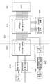
도 1은 본 발명의 실시예에 따른 고속 인터페이스 장치를 적용한 컴퓨터 시스템을 설명하기 위한 전체적인 블록 구성도이다.1 is an overall block diagram illustrating a computer system employing a high speed interface device according to an embodiment of the present invention.
도 1을 참조하면, 본 발명의 실시예에 따른 고속 인터페이스 장치를 적용한 컴퓨터 시스템(Computer System)은, 프로세서인 중앙처리장치(Central Processing Unit, CPU)(100), 메인보드 칩셋(Chipset)(200), 각종 입/출력포트(I/O port)(예컨대, USB 포트 등)(300), PCI(Peripheral Component Interconnect)/PCIE(Peripheral Component Interconnect Express) 등의 확장 슬롯(slot)(400), 바이오스(BIOS: Basic Input Output System)를 탑재한 롬(ROM) 또는 플래시(Flash) 메모리 등의 메인 메모리(500), 광 신호 전송을 지원하는 외부장치를 PCIE 슬롯을 통해 연결하기 위한 고속 인터페이스 장치(600), 기타 그래픽 카드(Graphic Card)(미도시), 사운드 카드(Sound Card)(미도시), 랜 카드(LAN Card)(미도시) 등의 주변 장치를 포함할 수 있다.Referring to FIG. 1, a computer system to which a high speed interface device according to an exemplary embodiment of the present invention is applied includes a central processing unit (CPU) 100 that is a processor and a
여기서, 컴퓨터 시스템 전체를 하드웨어적으로 제어하는 기능을 수행하는 메인보드 칩셋(200)은 노스 브리지 칩셋 (North Bridge Chipset)(210) 및 사우스 브리지 칩셋(South Bridge Chipset)(220)을 포함할 수 있다.Here, the
노스 브리지 칩셋(210)은 중앙처리장치(CPU)(100), 메인 메모리(500), PCIE 확장 슬롯, 그래픽 카드(미도시) 등의 고속으로 동작하는 장치를 제어하는 기능을 수행하는 칩셋이고, 사우스 브리지 칩셋(220)은 메인보드에 부착된 각 구성요소(예컨대, HDD, Audio Controller, BIOS ROM, Ethernet/Wireless LAN/Minicard, Turbo Memory, USB, Embeded Controller 등) 사이의 입/출력을 제어하는 기능을 수행하는 칩셋이다.The
예를 들면, 노스 브리지 칩셋(210) 및 사우스 브리지 칩셋(220)의 구성은 예컨대, 인텔사, AMD사, nVIDIA사, VIS사, SIS사 등의 제품으로 구성할 수 있다.For example, the configurations of the
특히, 본 발명에 따른 고속 인터페이스 장치(600)는, 컴퓨터 시스템 내부의 중앙처리장치(CPU)(100)와 광 신호 전송을 지원하는 외부장치간에 고속의 신호처리를 지원하는 PCIE 방식을 이용하여 서로 연결하기 위한 장치로서, 컴퓨터의 메인보 드에 연결되는 슬롯과, 상기 슬롯에서의 신호를 적합하게 제어하는 제어모듈, 상기 제어모듈로부터 제어된 신호를 광 신호 전송에 적합한 신호로 변환해주는 신호처리모듈, 상기 신호처리모듈로부터 처리된 전기신호를 광 신호로 변환해주는 광/전 변환모듈, 상기 광 신호를 전송하는 광전송수단 등으로 구성된다.In particular, the high-
도 2는 본 발명의 일 실시예에 따른 광 연결을 이용한 고속 인터페이스 장치를 구체적으로 설명하기 위한 블록 구성도이고, 도 3은 본 발명의 실시예에 적용된 광연결모듈을 설명하기 위한 평면도이다.FIG. 2 is a block diagram illustrating a high speed interface device using an optical connection according to an embodiment of the present invention in detail. FIG. 3 is a plan view illustrating an optical connection module applied to an embodiment of the present invention.
도 2 및 도 3을 참조하면, 본 발명의 일 실시예에 따른 광 연결을 이용한 고속 인터페이스 장치(600)는, 크게 광연결모듈(610), 광/전 변환모듈(620), 신호처리모듈(630), PCIE 제어모듈(640) 및 PCIE 슬롯(650) 등을 포함하여 이루어진다.2 and 3, the high
여기서, 광연결모듈(610)은 광 시리얼 버스(Optical Serial Bus, OSB)라고도 칭하며, 광 신호를 전송하기 위한 신호 전송 수단으로서 광의적으로는 광 신호를 전송하는 광 PCB(Printed Circuit Board)와, 본 발명의 고속 인터페이스 장치를 외부와 연결하는 포트의 물리적 장치와 이를 통해 광 신호를 전송하는 것을 모두 포함할 수 있으나, 본 발명에서는 외부에 광 신호를 전송할 수 있도록 암/수 포트(Port) 즉, 제1 및 제2 광연결부재(611 및 612)를 지칭하기로 한다.Here, the
도 3에 도시된 바와 같이, 광연결모듈(610)은 광 신호가 입/출력되도록 외부장치를 연결하기 위한 것으로서, 제1 및 제2 광연결부재(611 및 612)로 구성되어 있다.As shown in FIG. 3, the
제1 광연결부재(611)는 예컨대, 적어도 하나의 광섬유(Optical fiber) 또는 광도파로가 적층된 광전송로(611-1)와 적어도 하나의 가이드 홀(Guide Hole)(611-2)이 형성된 MT 페룰(ferrule) 혹은 이에 상응하는 제1 커넥터(Connector)(611-3)로 구성되어 있다.The first
제2 광연결부재(612)는 예컨대, 적어도 하나의 광섬유(Optical fiber) 또는 광도파로가 적층된 광전송로(612-1)와 가이드 홀(611-2)에 삽입되는 가이드 핀(Guide Pin)(612-2)이 형성된 MT 페룰(ferrule) 혹은 이에 상응하는 제2 커넥터(612-3)로 구성되어 있다.The second optical connecting
즉, 제2 연결부재(611 및 612)는 내부에 가이드 핀(612-2)과 광전송로(612-1)를 일정한 거리로 유지시켜 고정시킴과 동시에 외부장치와 연결되어 본 발명의 고속 인터페이스 장치를 지지해주는 작용을 한다. 그리고, 가이드 핀(612-2)은 가이드 홀(611-2)에 연결되어 본 발명의 고속 인터페이스 장치를 지지하는 작용을 하며, 광전송로(611-1 및 612-1)는 광 신호를 외부장치에 송수신하는 작용을 수행한다.That is, the
한편, 가이드 홀(611-2) 및 가이드 핀(612-2)은 전력선(611-4 및 612-4)을 통해 PCIE 슬롯(650)의 전원단자(PWR) 및 접지(GND)에 연결되어 외부장치에 전원이 공급되도록 할 수 있다(도 4 참조).Meanwhile, the guide hole 611-2 and the guide pin 612-2 are connected to the power terminal PWR and ground GND of the
광/전 변환모듈(620)은 광전송모듈(615)을 통해 광연결모듈(610)과 연결되어 있으며, 광연결모듈(610)로부터 전송된 광 신호를 전기신호로 변환하거나 전기신호를 광 신호로 변환하는 기능을 수행한다.The optical /
이러한 광/전 변환모듈(620)은 광 신호에 반응하여 전기신호로 변환시켜주는 포토 디텍터(Photo Detector), 레이저 다이오드(Laser Diode) 및 이를 적절한 수준의 전기신호로 송수신하게 하는 드라이버(Driver) IC, 리시버(Receiver) IC 등으로 구성될 수 있다.The photo /
즉, 광/전 변환모듈(620)은 광전송모듈(615)을 통해 수신된 광 신호를 전기신호로 변환하거나, 신호처리모듈(630)에서의 전기신호를 광 신호로 변환하는 작용을 하는데, 수신된 광 신호는 상기 포토 디텍터를 통해 전기신호로 변환되어 상기 리시버 IC에서 적합한 신호 처리를 거친 후 신호처리모듈(630)로 송신되고, 신호처리모듈(630)로부터 수신한 전기신호의 경우 상기 드라이버 IC와 레이저 다이오드를 통해 광 신호로 변환되어 광연결모듈(610)로 전송된다.That is, the
그리고, 광전송모듈(615)은 광연결모듈(610)의 광 신호를 광/전 변환모듈(620)로 연결시켜주는 일명 광 링크(Optical Link)로서, 본 발명에서의 광전송로로 한정하기로 하며, 바람직하게는 PCB에 적층된 형태의 광섬유이지만 예컨대, 웨이브-가이드(Wave Guide)나 폴리머(Polymer) 등을 이용하여 적층하거나 적층하지 않고 광도파로들을 광전송로로 사용할 수도 있다.In addition, the
즉, 광전송모듈(615)은 전술한 바와 같이 광섬유가 적층된 광 PCB 혹은 동일한 작용을 할 수 있는 광도파로로서, 광연결모듈(610)의 광 신호를 광/전 변환모듈(620)로 전송하는 작용을 한다.That is, the
신호처리모듈(630)은 광/전 변환모듈(620)과 전기적인 링크(Electrical Link)(예컨대, 전력선 등)(625)를 통해 연결되어 있으며, 예컨대, 직렬 전기신호를 병렬 전기신호로 분할하거나 병렬 전기신호를 직결 전기신호로 취합하도록 신호처리를 수행하는 기능을 수행한다.The
이러한 신호처리모듈(630)은 서데스(SerDes, Serializer and Deserializer) 혹은 이에 상응하는 먹싱/디먹싱(Muxing/DeMuxing) 기능을 수행하는 장치와 이의 작용을 클럭(Clock)에 맞춰 적합하게 도와주는 장치 등으로 이루어질 수 있다.The
즉, 신호처리모듈(630)은 고속의 신호를 PCIE 제어모듈(640)의 처리 속도에 맞는 신호로 분할하거나 그 반대로 PCIE 제어모듈(640)의 신호를 고속의 신호로 취합하는 작용을 한다.That is, the
이때, 전기신호를 취합하거나 분할하는 작용은 상기 서데스(SerDes)에서 이루어지며, 상기 서데스(SerDes)에서 이러한 작용을 적합하게 이루어지게 할 수 있도록 예컨대, PLL, 클럭(Clock) 등의 회로들이 상기 서데스(SerDes)에 연결되어 신호를 보정하는 작용을 수행한다.At this time, the action of collecting or dividing an electrical signal is performed in the SerDes, and circuits such as a PLL and a clock may be used to make such an operation suitably in the Serdes. It is connected to the SerDes to perform a function of correcting a signal.
PCIE 제어모듈(640)은 신호처리모듈(630)과 전기적인 링크(625)를 통해 연결되어 있으며, 신호처리모듈(630)로부터 처리된 신호를 제어하여 PCIE 슬롯(650)을 통해 상기 중앙처리장치(CPU)로 전달함과 아울러 상기 중앙처리장치(CPU)와 상기 외부장치간에 송수신되는 고속의 데이터를 제어하는 기능을 수행한다.The
즉, PCIE 제어모듈(640)은 PCIE 슬롯(650)을 통해 컴퓨터 시스템의 메인보드의 노스 브릿지 칩셋(210, 도 1 참조)에 연결되어 신호를 송수신함에 있어 신호 체계에 따른 올바른 작용을 할 수 있도록 제어하는 작용을 수행한다.That is, the
한편, PCIE 슬롯(650)은 PCIE의 표준에 맞는 규격의 전기신호 전송로로 구성 되어 있으며, 본 발명에서 언급한 PCB는 예컨대, 다층 FR4 혹은 세라믹(Seramic) 등의 고속 신호 전송에 적합한 재질로 제조될 수 있다.On the other hand, the
도 4는 본 발명의 다른 실시예에 따른 광 연결을 이용한 고속 인터페이스 장치를 구체적으로 설명하기 위한 블록 구성도로서, 광 신호 전송을 지원하는 외부장치와 전기신호 전송을 지원하는 외부장치를 함께 사용할 경우를 나타낸 블록 구성도이다.FIG. 4 is a block diagram illustrating a high speed interface device using an optical connection according to another embodiment of the present invention in detail. When an external device supporting optical signal transmission and an external device supporting electrical signal transmission are used together, FIG. It is a block diagram showing the following.
도 4를 참조하면, 본 발명의 다른 실시예에 따른 광 연결을 이용한 고속 인터페이스 장치(600')는, 크게 광연결모듈(610), 광/전 변환모듈(620), 신호처리모듈(630), PCIE 제어모듈(640), PCIE 슬롯(650), 스위치부(660) 및 전기 슬롯부(670) 등을 포함하여 이루어진다.Referring to FIG. 4, the high
여기서, 광연결모듈(610), 광/전 변환모듈(620), 신호처리모듈(630), PCIE 제어모듈(640) 및 PCIE 슬롯(650)은 전술한 본 발명의 일 실시예와 동일한 구성요소로서, 이에 대한 상세한 설명은 생략하기로 한다.Here, the
스위치부(660)는 광/전 변환모듈(620)과 신호처리모듈(630) 사이에 전기적인 링크(Electrical Link)(625)를 통해 연결되어 있으며, 광연결모듈(610)에 연결된 외부장치와 전기 슬롯부(670)에 연결된 외부장치의 입/출력 신호에 따라 신호처리모듈(630)을 전기 슬롯부(670) 또는 광/전 변환모듈(620)에 선택적으로 연결되도록 스위칭하는 기능을 수행한다.The
전기 슬롯부(670)는 전기적인 링크(665)를 통해 스위치부(660)와 연결되어 있으며, 전기신호 전송을 지원하는 외부장치(예컨대, USB 장치)와 연결하기 위한 전송로의 작용을 수행한다.The
상기와 같이 구성된 본 발명의 다른 실시예에 따른 고속 인터페이스 장치는, 광/전 변환모듈(620)과 신호처리모듈(630) 사이에 스위치부(660)가 구성되어, 외부장치가 지원하는 포트와 신호 체계에 따라 외부 두 개의 입/출력 단자와의 연결을 선택하도록 구성되어 있다.In the high-speed interface device according to another embodiment of the present invention configured as described above, a
만약, 스위치부(660)가 전기적인 링크(665)에 연결될 경우, 전기신호 전송을 지원하는 외부장치(예컨대, USB 장치)의 신호를 신호처리모듈(630)에 통신하여 신호 체계에 적합한 신호 체계 변환 과정을 거쳐 PCIE 슬롯(650)에 전달하게 되며, 스위치부(660)가 광 링크(Optical Link)인 광전송모듈(615)을 통해 연결될 경우 전술한 본 발명의 일 실시예와 같은 작용을 하게 된다.If the
한편, 본 발명의 실시예들에 따른 고속 인터페이스 장치는 바람직하게 PCIE 슬롯(650)에 연결되는데, PCIE가 노스 브리지 칩셋(210)에 직접 연결됨으로써, 비교적 고속의 데이터 전송을 수행할 수 있기 때문이다.On the other hand, the high speed interface device according to the embodiments of the present invention is preferably connected to the
즉, 본 발명은 고속의 데이터 전송을 수행할 수 있는 PCIE의 특징을 이용하여 PCIE와 USB 3.0을 연결하는 용도 혹은 고속의 광 전송을 하는 외부장치를 PCIE 슬롯(650)을 이용하여 컴퓨터 시스템의 노스 브리지 칩셋(210)에 연결하는 작용을 수행한다.That is, the present invention uses the PCIE and USB 3.0 to use the features of the PCIE capable of performing high-speed data transmission, or the North of the computer system using the
상기와 같은 본 발명은 USB 3.0 등의 고속 데이터 전송을 지원하는 차세대 이동식 장치와 고속의 광 신호 전송을 지원하는 장치를 컴퓨터 시스템에 적합하게 연결될 수 있는 장치를 제공하는 효과를 가진다.The present invention as described above has the effect of providing a device that can be suitably connected to a next-generation mobile device that supports high-speed data transmission, such as USB 3.0 and a device that supports high-speed optical signal transmission to a computer system.
또한, 본 발명에 의하면, 현 시점에서 가장 빠른 외부장치 연결을 제공하는 PCIE와 외부장치를 연결할 수 있는 장치를 제공함으로써, 외부장치 본래의 데이터 전송 속도의 손실을 막을 수 있으며, 이는 기술이 발달함에 따라 PCIE가 아닌 다른 형식의 슬롯(slot)이 될 수도 있다.In addition, according to the present invention, by providing a device capable of connecting the PCIE and the external device that provides the fastest external device connection at this time, it is possible to prevent the loss of the original data transmission speed of the external device, which is due to the development of technology Therefore, it may be a slot of a type other than PCIE.
또한, 본 발명에 의하면, 광 연결을 적용함으로써 임피던스 미스 매칭에 의한 왜곡 현상과 고속 전송에서 쉽게 일어나는 데이터의 불안정성을 상당 부분 해소할 수 있으며, 이는 고속의 차세대 컴퓨터 개발에 이바지할 수 있는 효과가 있다.In addition, according to the present invention, by applying the optical connection can significantly solve the distortion caused by impedance mismatch and instability of data easily occurring in high-speed transmission, which can contribute to the development of high-speed next-generation computer .
전술한 본 발명에 따른 광 연결을 이용한 고속 인터페이스 장치에 대한 바람직한 실시예에 대하여 설명하였지만, 본 발명은 이에 한정되는 것이 아니고 특허청구범위와 발명의 상세한 설명 및 첨부한 도면의 범위 안에서 여러 가지로 변형하여 실시하는 것이 가능하고 이 또한 본 발명에 속한다.Although a preferred embodiment of the high speed interface apparatus using the optical connection according to the present invention described above has been described, the present invention is not limited to this, but various modifications within the scope of the claims and the detailed description of the invention and the accompanying drawings. It is possible to carry out by this and this also belongs to the present invention.
도 1은 본 발명의 실시예에 따른 고속 인터페이스 장치를 적용한 컴퓨터 시스템을 설명하기 위한 전체적인 블록 구성도이다.1 is an overall block diagram illustrating a computer system employing a high speed interface device according to an embodiment of the present invention.
도 2는 본 발명의 일 실시예에 따른 광 연결을 이용한 고속 인터페이스 장치를 구체적으로 설명하기 위한 블록 구성도이다.2 is a block diagram illustrating in detail a high speed interface device using an optical connection according to an embodiment of the present invention.
도 3은 본 발명의 실시예에 적용된 광연결모듈을 설명하기 위한 평면도이다.3 is a plan view illustrating an optical connection module applied to an embodiment of the present invention.
도 4는 본 발명의 다른 실시예에 따른 광 연결을 이용한 고속 인터페이스 장치를 구체적으로 설명하기 위한 블록 구성도이다.4 is a block diagram illustrating in detail a high speed interface device using an optical connection according to another embodiment of the present invention.
Claims (7)
Translated fromKoreanPriority Applications (2)
| Application Number | Priority Date | Filing Date | Title |
|---|---|---|---|
| KR1020090110105AKR101220464B1 (en) | 2009-11-16 | 2009-11-16 | Express interface apparatus using optical connection |
| US12/696,668US20110116807A1 (en) | 2009-11-16 | 2010-01-29 | Express interface apparatus using optical connection |
Applications Claiming Priority (1)
| Application Number | Priority Date | Filing Date | Title |
|---|---|---|---|
| KR1020090110105AKR101220464B1 (en) | 2009-11-16 | 2009-11-16 | Express interface apparatus using optical connection |
Publications (2)
| Publication Number | Publication Date |
|---|---|
| KR20110053536A KR20110053536A (en) | 2011-05-24 |
| KR101220464B1true KR101220464B1 (en) | 2013-01-10 |
Family
ID=44011365
Family Applications (1)
| Application Number | Title | Priority Date | Filing Date |
|---|---|---|---|
| KR1020090110105AExpired - Fee RelatedKR101220464B1 (en) | 2009-11-16 | 2009-11-16 | Express interface apparatus using optical connection |
Country Status (2)
| Country | Link |
|---|---|
| US (1) | US20110116807A1 (en) |
| KR (1) | KR101220464B1 (en) |
Families Citing this family (17)
| Publication number | Priority date | Publication date | Assignee | Title |
|---|---|---|---|---|
| US8661268B2 (en)* | 2010-02-22 | 2014-02-25 | Apple Inc. | Methods and apparatus for intelligently providing power to a device |
| TWI514151B (en)* | 2011-12-12 | 2015-12-21 | Hon Hai Prec Ind Co Ltd | Computer and computer data transmitting system thereof |
| CN103164373B (en)* | 2011-12-14 | 2017-12-12 | 赛恩倍吉科技顾问(深圳)有限公司 | Computer and its data transfer of computer system |
| CN103164377A (en)* | 2011-12-19 | 2013-06-19 | 鸿富锦精密工业(深圳)有限公司 | Computer data transmission system and computer mainboard thereof |
| US9043526B2 (en)* | 2012-06-20 | 2015-05-26 | International Business Machines Corporation | Versatile lane configuration using a PCIe PIe-8 interface |
| CN103392305A (en)* | 2012-12-26 | 2013-11-13 | 华为技术有限公司 | Pcie signal transmission method and apparatus |
| WO2015027320A1 (en)* | 2013-08-29 | 2015-03-05 | Dan Oprea | Method and apparatus to manage the direct interconnect switch wiring and growth in computer networks |
| KR102339060B1 (en) | 2014-11-12 | 2021-12-14 | 주식회사 바텍 | Digital X-Ray Imaging Apparatus And Digital X-Ray Imaging System Comprising The Same |
| US9501118B2 (en)* | 2014-11-19 | 2016-11-22 | Dell Products L.P. | Information handling system multi-purpose connector guide pin structure |
| US9891680B2 (en)* | 2014-11-19 | 2018-02-13 | Dell Products L.P. | Information handling system multi-purpose connector guide pin structure |
| US9791906B2 (en) | 2014-11-19 | 2017-10-17 | Dell Products L.P. | Information handling system multi-purpose connector guide pin structure |
| US10320128B2 (en) | 2014-11-19 | 2019-06-11 | Dell Products L.P. | Information handling system multi-purpose connector guide pin structure |
| KR102340667B1 (en) | 2015-10-08 | 2021-12-20 | 삼성전자주식회사 | Apparatus for Processing Video, Driving Method of Apparatus for Processing Video, and Computer Readable Recording Medium |
| US10797797B2 (en)* | 2017-03-31 | 2020-10-06 | Nexans | Fiber optic extender |
| US10789188B1 (en)* | 2019-02-08 | 2020-09-29 | Facebook, Inc. | Systems and methods for providing semi-custom printed circuit boards based on standard interconnections |
| KR20200139643A (en) | 2019-06-04 | 2020-12-14 | 한국과학기술원 | Apparatus for interfacing optical using optical Printed Circuit Board with built-in optical waveguide |
| CN116974829A (en)* | 2022-04-24 | 2023-10-31 | 富联精密电子(天津)有限公司 | Substrate management controller detection system and method |
Citations (3)
| Publication number | Priority date | Publication date | Assignee | Title |
|---|---|---|---|---|
| KR20000062142A (en)* | 1999-03-10 | 2000-10-25 | 윤종용 | Connector and Cable having Transducer and Receiver for Optical Transmission |
| JP2008065818A (en)* | 2006-09-07 | 2008-03-21 | Internatl Business Mach Corp <Ibm> | System and method for executing function of pci express function card away from data processing system |
| KR20090011545A (en)* | 2007-07-26 | 2009-02-02 | 주식회사 다산네트웍스 | Passive Optical Termination for Computer |
Family Cites Families (7)
| Publication number | Priority date | Publication date | Assignee | Title |
|---|---|---|---|---|
| US5293626A (en)* | 1990-06-08 | 1994-03-08 | Cray Research, Inc. | Clock distribution apparatus and processes particularly useful in multiprocessor systems |
| US7296936B2 (en)* | 2005-06-20 | 2007-11-20 | Intel Corporation | Method, apparatus, and system for using an optical link with electrical link receiver detection |
| GB0524217D0 (en)* | 2005-11-28 | 2006-01-04 | Amphotonix Ltd | Fibre-optic module |
| US7597592B2 (en)* | 2006-12-27 | 2009-10-06 | Intel Corporation | Automatic configuration of an interface to a host or client |
| CN101335736B (en)* | 2007-06-28 | 2011-05-25 | 联想(北京)有限公司 | High-speed peripheral interconnecting interface |
| US8135282B2 (en)* | 2008-07-31 | 2012-03-13 | Finisar Corporation | Fiberoptic transceiver module with integral status indicators |
| KR100973079B1 (en)* | 2008-08-13 | 2010-07-29 | 한국전자통신연구원 | High speed PCI signal transmission device and control method |
- 2009
- 2009-11-16KRKR1020090110105Apatent/KR101220464B1/ennot_activeExpired - Fee Related
- 2010
- 2010-01-29USUS12/696,668patent/US20110116807A1/ennot_activeAbandoned
Patent Citations (3)
| Publication number | Priority date | Publication date | Assignee | Title |
|---|---|---|---|---|
| KR20000062142A (en)* | 1999-03-10 | 2000-10-25 | 윤종용 | Connector and Cable having Transducer and Receiver for Optical Transmission |
| JP2008065818A (en)* | 2006-09-07 | 2008-03-21 | Internatl Business Mach Corp <Ibm> | System and method for executing function of pci express function card away from data processing system |
| KR20090011545A (en)* | 2007-07-26 | 2009-02-02 | 주식회사 다산네트웍스 | Passive Optical Termination for Computer |
Also Published As
| Publication number | Publication date |
|---|---|
| KR20110053536A (en) | 2011-05-24 |
| US20110116807A1 (en) | 2011-05-19 |
Similar Documents
| Publication | Publication Date | Title |
|---|---|---|
| KR101220464B1 (en) | Express interface apparatus using optical connection | |
| EP2375340B1 (en) | Apparatus interoperable with backward compatible optical USB device | |
| EP2375339B1 (en) | Backward compatible optical USB device | |
| CN100507890C (en) | Intermediate devices capable of communicating using different communication protocols | |
| CN103827841B (en) | IO connector with configurable bandwidth | |
| US8224185B2 (en) | USB compatible apparatus for connecting between optical USB device and electrical USB device | |
| CN111538689B (en) | Multi-channel PCIE (peripheral component interface express) adapter card with two heterogeneous ends | |
| CN103246314A (en) | Mainboard with expansion connector | |
| EP3637270A1 (en) | External electrical connector and computer system | |
| CN105898493A (en) | Asynchronous receiver transmitter and USB interface multiplexing circuit and circuit board | |
| CN110362058A (en) | The system tested for multiple interfaces | |
| US20120096286A1 (en) | Charging management method, charging control circuit and the host apparatus having the same | |
| CN102096457B (en) | processing device and operating system | |
| CN107707362B (en) | A transfer card, structure and method supporting 100G network | |
| TWI428759B (en) | Optical usb device and operation method | |
| CN114840461B (en) | Expansion device of server and server | |
| CN107480085A (en) | Multiplex roles integrated test system | |
| CN204360266U (en) | riser card | |
| US8583849B2 (en) | Signal switch connector set applied to motherboard of computer system | |
| CN115952120A (en) | Interface switching device, mainboard interface expansion circuit and computer equipment | |
| CN116107943A (en) | Signal transmission circuit and computing equipment | |
| US9928198B2 (en) | Adapter card with a computer module form factor | |
| TWI512482B (en) | Motherboard assembly and information handling system thereof | |
| CN103631749B (en) | expansion module | |
| CN221899552U (en) | Computer motherboard and computer |
Legal Events
| Date | Code | Title | Description |
|---|---|---|---|
| A201 | Request for examination | ||
| PA0109 | Patent application | St.27 status event code:A-0-1-A10-A12-nap-PA0109 | |
| PA0201 | Request for examination | St.27 status event code:A-1-2-D10-D11-exm-PA0201 | |
| D13-X000 | Search requested | St.27 status event code:A-1-2-D10-D13-srh-X000 | |
| D14-X000 | Search report completed | St.27 status event code:A-1-2-D10-D14-srh-X000 | |
| E902 | Notification of reason for refusal | ||
| PE0902 | Notice of grounds for rejection | St.27 status event code:A-1-2-D10-D21-exm-PE0902 | |
| AMND | Amendment | ||
| E13-X000 | Pre-grant limitation requested | St.27 status event code:A-2-3-E10-E13-lim-X000 | |
| P11-X000 | Amendment of application requested | St.27 status event code:A-2-2-P10-P11-nap-X000 | |
| P13-X000 | Application amended | St.27 status event code:A-2-2-P10-P13-nap-X000 | |
| PG1501 | Laying open of application | St.27 status event code:A-1-1-Q10-Q12-nap-PG1501 | |
| E601 | Decision to refuse application | ||
| PE0601 | Decision on rejection of patent | St.27 status event code:N-2-6-B10-B15-exm-PE0601 | |
| AMND | Amendment | ||
| E13-X000 | Pre-grant limitation requested | St.27 status event code:A-2-3-E10-E13-lim-X000 | |
| P11-X000 | Amendment of application requested | St.27 status event code:A-2-2-P10-P11-nap-X000 | |
| P13-X000 | Application amended | St.27 status event code:A-2-2-P10-P13-nap-X000 | |
| PX0901 | Re-examination | St.27 status event code:A-2-3-E10-E12-rex-PX0901 | |
| PX0601 | Decision of rejection after re-examination | St.27 status event code:N-2-6-B10-B17-rex-PX0601 | |
| J201 | Request for trial against refusal decision | ||
| PJ0201 | Trial against decision of rejection | St.27 status event code:A-3-3-V10-V11-apl-PJ0201 | |
| PJ1301 | Trial decision | St.27 status event code:A-3-3-V10-V15-crt-PJ1301 Decision date:20121217 Appeal event data comment text:Appeal Kind Category : Appeal against decision to decline refusal, Appeal Ground Text : 2009 0110105 Appeal request date:20120116 Appellate body name:Patent Examination Board Decision authority category:Office appeal board Decision identifier:2012101000443 | |
| PS0901 | Examination by remand of revocation | St.27 status event code:A-6-3-E10-E12-rex-PS0901 | |
| PS0701 | Decision of registration after remand of revocation | St.27 status event code:A-3-4-F10-F13-rex-PS0701 | |
| GRNT | Written decision to grant | ||
| PR0701 | Registration of establishment | St.27 status event code:A-2-4-F10-F11-exm-PR0701 | |
| PR1002 | Payment of registration fee | St.27 status event code:A-2-2-U10-U11-oth-PR1002 Fee payment year number:1 | |
| PG1601 | Publication of registration | St.27 status event code:A-4-4-Q10-Q13-nap-PG1601 | |
| R18-X000 | Changes to party contact information recorded | St.27 status event code:A-5-5-R10-R18-oth-X000 | |
| PN2301 | Change of applicant | St.27 status event code:A-5-5-R10-R13-asn-PN2301 St.27 status event code:A-5-5-R10-R11-asn-PN2301 | |
| R18-X000 | Changes to party contact information recorded | St.27 status event code:A-5-5-R10-R18-oth-X000 | |
| FPAY | Annual fee payment | Payment date:20151229 Year of fee payment:4 | |
| PR1001 | Payment of annual fee | St.27 status event code:A-4-4-U10-U11-oth-PR1001 Fee payment year number:4 | |
| FPAY | Annual fee payment | Payment date:20170110 Year of fee payment:5 | |
| PR1001 | Payment of annual fee | St.27 status event code:A-4-4-U10-U11-oth-PR1001 Fee payment year number:5 | |
| PC1903 | Unpaid annual fee | St.27 status event code:A-4-4-U10-U13-oth-PC1903 Not in force date:20180104 Payment event data comment text:Termination Category : DEFAULT_OF_REGISTRATION_FEE | |
| FPAY | Annual fee payment | Payment date:20180808 Year of fee payment:6 | |
| K11-X000 | Ip right revival requested | St.27 status event code:A-6-4-K10-K11-oth-X000 | |
| PC1903 | Unpaid annual fee | St.27 status event code:N-4-6-H10-H13-oth-PC1903 Ip right cessation event data comment text:Termination Category : DEFAULT_OF_REGISTRATION_FEE Not in force date:20180104 | |
| PR0401 | Registration of restoration | St.27 status event code:A-6-4-K10-K13-oth-PR0401 | |
| PR1001 | Payment of annual fee | St.27 status event code:A-4-4-U10-U11-oth-PR1001 Fee payment year number:6 | |
| R401 | Registration of restoration | ||
| LAPS | Lapse due to unpaid annual fee | ||
| PC1903 | Unpaid annual fee | St.27 status event code:A-4-4-U10-U13-oth-PC1903 Not in force date:20190104 Payment event data comment text:Termination Category : DEFAULT_OF_REGISTRATION_FEE | |
| R18-X000 | Changes to party contact information recorded | St.27 status event code:A-5-5-R10-R18-oth-X000 | |
| PC1903 | Unpaid annual fee | St.27 status event code:N-4-6-H10-H13-oth-PC1903 Ip right cessation event data comment text:Termination Category : DEFAULT_OF_REGISTRATION_FEE Not in force date:20190104 | |
| PN2301 | Change of applicant | St.27 status event code:A-5-5-R10-R13-asn-PN2301 St.27 status event code:A-5-5-R10-R11-asn-PN2301 | |
| R18-X000 | Changes to party contact information recorded | St.27 status event code:A-5-5-R10-R18-oth-X000 | |
| R18-X000 | Changes to party contact information recorded | St.27 status event code:A-5-5-R10-R18-oth-X000 | |
| R18-X000 | Changes to party contact information recorded | St.27 status event code:A-5-5-R10-R18-oth-X000 |