KR101216381B1 - Method of forming thin film - Google Patents
Method of forming thin filmDownload PDFInfo
- Publication number
- KR101216381B1 KR101216381B1KR1020050126906AKR20050126906AKR101216381B1KR 101216381 B1KR101216381 B1KR 101216381B1KR 1020050126906 AKR1020050126906 AKR 1020050126906AKR 20050126906 AKR20050126906 AKR 20050126906AKR 101216381 B1KR101216381 B1KR 101216381B1
- Authority
- KR
- South Korea
- Prior art keywords
- nitrogen
- thin film
- boron
- gas
- containing gas
- Prior art date
- Legal status (The legal status is an assumption and is not a legal conclusion. Google has not performed a legal analysis and makes no representation as to the accuracy of the status listed.)
- Active
Links
Images


Classifications
- H—ELECTRICITY
- H01—ELECTRIC ELEMENTS
- H01L—SEMICONDUCTOR DEVICES NOT COVERED BY CLASS H10
- H01L21/00—Processes or apparatus adapted for the manufacture or treatment of semiconductor or solid state devices or of parts thereof
- H01L21/02—Manufacture or treatment of semiconductor devices or of parts thereof
- H01L21/02104—Forming layers
- H01L21/02107—Forming insulating materials on a substrate
- H01L21/02225—Forming insulating materials on a substrate characterised by the process for the formation of the insulating layer
- H01L21/0226—Forming insulating materials on a substrate characterised by the process for the formation of the insulating layer formation by a deposition process
- H01L21/02263—Forming insulating materials on a substrate characterised by the process for the formation of the insulating layer formation by a deposition process deposition from the gas or vapour phase
- H01L21/02271—Forming insulating materials on a substrate characterised by the process for the formation of the insulating layer formation by a deposition process deposition from the gas or vapour phase deposition by decomposition or reaction of gaseous or vapour phase compounds, i.e. chemical vapour deposition
- H01L21/0228—Forming insulating materials on a substrate characterised by the process for the formation of the insulating layer formation by a deposition process deposition from the gas or vapour phase deposition by decomposition or reaction of gaseous or vapour phase compounds, i.e. chemical vapour deposition deposition by cyclic CVD, e.g. ALD, ALE, pulsed CVD
- H—ELECTRICITY
- H01—ELECTRIC ELEMENTS
- H01L—SEMICONDUCTOR DEVICES NOT COVERED BY CLASS H10
- H01L21/00—Processes or apparatus adapted for the manufacture or treatment of semiconductor or solid state devices or of parts thereof
- H01L21/02—Manufacture or treatment of semiconductor devices or of parts thereof
- H01L21/02104—Forming layers
- H01L21/02107—Forming insulating materials on a substrate
- H01L21/02109—Forming insulating materials on a substrate characterised by the type of layer, e.g. type of material, porous/non-porous, pre-cursors, mixtures or laminates
- H01L21/02112—Forming insulating materials on a substrate characterised by the type of layer, e.g. type of material, porous/non-porous, pre-cursors, mixtures or laminates characterised by the material of the layer
- H01L21/02123—Forming insulating materials on a substrate characterised by the type of layer, e.g. type of material, porous/non-porous, pre-cursors, mixtures or laminates characterised by the material of the layer the material containing silicon
- H—ELECTRICITY
- H01—ELECTRIC ELEMENTS
- H01L—SEMICONDUCTOR DEVICES NOT COVERED BY CLASS H10
- H01L21/00—Processes or apparatus adapted for the manufacture or treatment of semiconductor or solid state devices or of parts thereof
- H01L21/02—Manufacture or treatment of semiconductor devices or of parts thereof
- H01L21/02104—Forming layers
- H01L21/02107—Forming insulating materials on a substrate
- H01L21/02296—Forming insulating materials on a substrate characterised by the treatment performed before or after the formation of the layer
- H01L21/02318—Forming insulating materials on a substrate characterised by the treatment performed before or after the formation of the layer post-treatment
- H01L21/02337—Forming insulating materials on a substrate characterised by the treatment performed before or after the formation of the layer post-treatment treatment by exposure to a gas or vapour
Landscapes
- Engineering & Computer Science (AREA)
- Physics & Mathematics (AREA)
- Condensed Matter Physics & Semiconductors (AREA)
- General Physics & Mathematics (AREA)
- Manufacturing & Machinery (AREA)
- Computer Hardware Design (AREA)
- Microelectronics & Electronic Packaging (AREA)
- Power Engineering (AREA)
- Chemical & Material Sciences (AREA)
- Chemical Kinetics & Catalysis (AREA)
- Formation Of Insulating Films (AREA)
- Chemical Vapour Deposition (AREA)
Abstract
Translated fromKoreanDescription
Translated fromKorean도 1a 내지 도 1d는 본 발명의 제 1 실시예에 따른 박막 형성 방법을 설명하기 위한 단면도.1A to 1D are cross-sectional views illustrating a method of forming a thin film according to a first embodiment of the present invention.
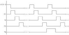
도 2는 본 실시예에 따른 박막 형성 방법을 위한 가스의 공급 순서를 도시한 도면.2 is a view showing a gas supply sequence for a thin film forming method according to the present embodiment.
도 3a 및 도 3b는 본 실시예의 변형예에 따른 박막 형성 방법을 설명하기 위한 단면도.3A and 3B are cross-sectional views for explaining a method of forming a thin film according to a modification of the present embodiment.
도 4a 내지 도 4c는 본 변형예에 따른 박막 형성 방법을 위한 가스의 공급 순서를 도시한 도면.4A to 4C are diagrams showing a supply sequence of gases for the thin film forming method according to the present modification.
도 5a 내지 도 5c는 본 발명의 제 2 실시예에 따른 박막 형성 방법을 설명하기 위한 단면도.5A to 5C are cross-sectional views illustrating a method of forming a thin film according to a second embodiment of the present invention.
<도면의 주요 부분에 대한 부호의 설명><Explanation of symbols for the main parts of the drawings>
110 : 기판120, 121, 122 : SiNx 막110
130, 131, 132 : BN막130, 131, 132: BN film
본 발명은 박막 형성 방법에 관한 것으로, 특히, BN/SiBN막의 막질을 향상시킬 수 있는 박막 형성 방법에 관한 것이다.The present invention relates to a thin film forming method, and more particularly, to a thin film forming method capable of improving the film quality of a BN / SiBN film.
반도체 제조공정 중 사용되는 절연 물질로는 SiNx는 실리콘 산화막에 대한 식각 선택비가 우수하고, 내마모성과 내 산화성 및 확산 배리어로서의 특성이 뛰어나 광범위하게 사용되었다. 하지만, 종래의 LPCVD방법으로 증착된 SiNx막은 그 유전 상수가 7로서 높기 때문에 소자의 크기 축소(65㎚이하)에 따른 기생 캐패시턴스의 증가로 인한 지연전달과 같은 문제를 유발하게 되었다.As an insulating material used in the semiconductor manufacturing process, SiNx has been widely used because of its excellent etching selectivity with respect to the silicon oxide film, its excellent wear resistance, oxidation resistance, and diffusion barrier properties. However, since the SiNx film deposited by the conventional LPCVD method has a high dielectric constant of 7, it causes problems such as delayed transfer due to an increase in parasitic capacitance due to the size reduction of the device (less than 65 nm).
이에 65㎚이하의 선폭을 갖는 반도체 소자에서는 LPCVD SiNx막 대신 낮은 유전 상수를 갖는 BN/SiBN막을 사용하고자 하는 노력이 활발히 진행중이다. 이러한 BN/SiBN막은 열 부담(thermal budget) 문제로 인해 550도 이하의 낮은 온도를 요구하고 있다. 그러나, 낮은 온도에서 BN/SiBN막이 증착되기 때문에 붕소(B) 및 질소(N)의 막내 함유량 조절이 용이하지 않은 문제가 있다. 즉, BN/SiBN막의 증착 조건에 따라 막의 유전율은 물론 막의 특성이 크게 변화하게 된다. 붕소의 농도에 따라 막의 식각율(막의 경화성)에 큰 차이가 있다. 이로인해 식각 배리어막으로 충분한 역할을 하지 못하게 되는 문제가 발생한다.Accordingly, efforts are being made to use BN / SiBN films having a low dielectric constant instead of LPCVD SiNx films in semiconductor devices having a line width of 65 nm or less. Such BN / SiBN films require low temperatures of 550 degrees or less due to thermal budget problems. However, since the BN / SiBN film is deposited at a low temperature, there is a problem that the in-film content control of boron (B) and nitrogen (N) is not easy. That is, the dielectric constant of the film and the properties of the film are greatly changed depending on the deposition conditions of the BN / SiBN film. There is a big difference in the etching rate (curability of the film) of the film according to the concentration of boron. This causes a problem that the etching barrier film does not play a sufficient role.
종래에는 이러한 문제를 해결하기 위한 방법으로 증착 온도를 높이거나, 붕소를 포함하는 기타 막을 구성하는 소스 가스들의 유입량을 변화시켜 붕소의 함유량을 조절하고자 하였다. 그러나, 종래에는 낮은 온도를 유지하면서 붕소의 농도를 조절하는 것이 매우 어려운 실정이었다.Conventionally, in order to solve this problem, the boron content is controlled by increasing the deposition temperature or by changing the inflow rate of source gases constituting the boron-containing film. However, in the past, it was very difficult to control the concentration of boron while maintaining a low temperature.
상술한 붕소 및 질소의 농도 조절을 위해 SiN/BN/SiBN 구조의 박막을 ALD 방법을 통해 증착한 다음 별도의 열처리 장치를 이용하여 SiN/BN/SiBN 구조의 박막을 열처리하였다. 그러나, ALD 방법을 적용한 공정에서는 N의 원료 가스로 NH3를 사용하게 되며, 이 경우 챔버 유입시 반응성을 고려하여 리모트 플라즈마(remote plasma)를 거쳐 챔버로 유입시키게 된다. 리모트 플라즈마를 사용하는 경우에는 NH3의 반응성 향상을 위해 마이크로 웨이브 방식의 장치를 장착하여 사용하는 경우가 많아지고 있다. 하지만 마이크로 웨이브 장치를 사용하는 경우 전체 증착 장비가 복잡해지고 추가 비용도 상당히 발생하여 제조 원가를 상승시키는 원인이 될 수 있다. 상술한 마스크로 웨이브 장치를 사용한 경우에도 N의 반응성이 불균일하여 막질의 개선에는 한계가 있다.In order to control the concentration of boron and nitrogen described above, a thin film of SiN / BN / SiBN structure was deposited through an ALD method, and then the thin film of SiN / BN / SiBN structure was heat-treated using a separate heat treatment apparatus. However, in the process using the ALD method, NH3 is used as a source gas of N. In this case, the reaction is introduced into the chamber via a remote plasma in consideration of the reactivity when the chamber is introduced. When using a remote plasma, there is a case of using a microwave method of mounting apparatus for improving the reactivity of NH3 increases. However, the use of microwave devices can complicate the overall deposition equipment and incur significant additional costs, leading to higher manufacturing costs. Even when the wave device is used as the mask described above, the reactivity of N is nonuniform and there is a limit to the improvement of the film quality.
또한, ALD를 이용하여 SiN/BN/SiBN 구조의 박막을 증착 한 다음 질소 함유 가스를 공급하면서 고온에서 열처리 공정을 실시하기로 하지만 이는 별도의 열처리 장치를 추가하여야 하고, 증착 후, 진공 파기 및 SiN/BN/SiBN 막이 증착된 기판의 이송 및 열처리 등의 공정 단계가 추가되어 박막 형성 공정이 복잡해지는 문제가 발생하고, 질소가 BN/SiBN막의 표면만을 트리트먼트 하여 막의 하부 및 내부 영역 의 막질이 향상되지 않게 된다.In addition, ALD is used to deposit a thin film of SiN / BN / SiBN structure and then perform a heat treatment process at a high temperature while supplying a nitrogen-containing gas, but this requires adding a separate heat treatment device, and after vacuum deposition and SiN Process steps such as transfer and heat treatment of the substrate on which the / BN / SiBN film is deposited are complicated, and the thin film forming process is complicated. Nitrogen treats only the surface of the BN / SiBN film to improve the film quality of the lower and inner regions of the film. Will not be.
이와 같이 종래의 BN/SiBN 박막의 형성 방법으로는 (B, N)결합비의 불균형에 의한 막질 저하로 인해 소자에서 요구하는 박막 특성을 얻는데 그 한계가 있고, 다수의 장치의 추가로 인한 제조 공정 단가가 상승되는 문제가 발생하였다.As described above, the conventional method of forming the BN / SiBN thin film has a limitation in obtaining thin film properties required by the device due to a decrease in film quality due to an imbalance in the (B, N) bonding ratio, and a manufacturing process due to the addition of a plurality of devices. There was a problem that the unit price increased.
따라서, 본 발명은 상기의 문제점을 해결하기 위하여 ALD를 이용하여 질소와 붕소를 포함하는 박막의 형성 전 또는 막 형성 과정 중 또는 막 형성 후에 구성 원소(B, N)중 하나를 이용한 트리트먼트를 실시하여 붕소와 질소의 결합비를 조절하여 막질을 향상시킬 수 있는 박막 형성 방법을 제공하는 것을 그 목적으로 한다.Therefore, in order to solve the above problems, the present invention performs treatment using one of the constituent elements (B, N) before, during or after the formation of a thin film containing nitrogen and boron using ALD. It is an object of the present invention to provide a method for forming a thin film which can improve the film quality by controlling the bonding ratio of boron and nitrogen.
본 발명에 따른 반도체 기판을 준비하는 단계와, 상기 반도체 기판 상에 붕소와 질소를 포함하는 1차 박막을 형성하는 단계와, 상기 붕소 또는 상기 질소 함유 가스로 트리트먼트를 실시하는 1차 가스 처리 단계와, 상기 1차 박막 상에 상기 붕소와 질소를 포함하는 2차 박막을 형성하는 단계와, 상기 붕소 또는 상기 질소 함유 가스로 트리트먼트를 실시하는 2차 가스 처리 단계를 포함하는 박막 형성 방법을 제공한다.Preparing a semiconductor substrate according to the present invention, forming a primary thin film containing boron and nitrogen on the semiconductor substrate, and the primary gas treatment step of performing a treatment with the boron or the nitrogen-containing gas And forming a secondary thin film containing boron and nitrogen on the primary thin film, and performing a secondary gas treatment step of treating with the boron or the nitrogen-containing gas. do.
상술한 상기 박막을 형성하는 단계와, 상기 가스 처리하는 단계를 인시츄로 다수번 반복 실시하는 것이 바람직하다.It is preferable to repeatedly perform the above-described step of forming the thin film and the gas treatment in situ a plurality of times.
상기의 박막은 ALD 공정을 통해 형성되고, 상기 가스 처리 단계는 증착되는 박막의 매 10 내지 40Å 두께마다 실시하는 것이 바람지하다.The thin film is formed through an ALD process, and the gas treatment step is preferably performed every 10 to 40 mm thick of the thin film to be deposited.
그리고 상기 가스 처리 단계는 상기 붕소 또는 질소 함유 가스를 플라즈마를 이용하여 활성화시켜 상기 박막에 공급하는 것이 바람직하다.In the gas treatment step, the boron or nitrogen-containing gas may be activated by using a plasma and supplied to the thin film.
물론 상기 가스 처리 단계는 상기 붕소 또는 질소 함유 가스를 상기 박막에 공급하고 열처리하는 것이 효과적이다.Of course, the gas treatment step is effective to supply the boron or nitrogen-containing gas to the thin film and heat treatment.
이때, 상기 1차 및 2차 박막 중 적어도 어느 하나의 박막은 실리콘을 더 포함하는 것이 바람직하다.In this case, it is preferable that at least one thin film of the primary and secondary thin films further includes silicon.
상기 질소 함유 가스로는 N2, NH3, N2H2, N2O, NO2 중 적어도 어느 하나를 사용하고, 상기 붕소 함유 가스로 BCl3, BBr3, B2H6 또는 BF3 중 적어도 어느 하나를 사용하는 것이 바람직하다.At least one of N2 , NH3 , N2 H2 , N2 O, and NO2 is used as the nitrogen-containing gas, and at least one of BCl3 , BBr3 , B2 H6, or BF3 is used as the boron-containing gas. It is preferable to use either.
또한, 본 발명에 따른 반도체 기판을 준비하는 단계와, 상기 반도체 기판을 활성화된 붕소 또는 질소 함유 가스를 이용하여 표면 처리하는 단계와, 상기 표면 처리된 상기 반도체 기판 상에 붕소와 질소를 포함하는 박막을 형성하는 단계와, 상기 붕소 또는 상기 질소 함유 가스로 트리트먼트를 실시하는 가스 처리 단계를 포함하는 박막 형성 방법을 제공한다.In addition, preparing a semiconductor substrate according to the present invention, surface-treating the semiconductor substrate using an activated boron or nitrogen-containing gas, and a thin film containing boron and nitrogen on the surface-treated semiconductor substrate And forming a gas treatment step of treating the boron or the nitrogen-containing gas.
이하, 첨부된 도면을 참조하여 본 발명의 실시예를 더욱 상세히 설명하기로 한다. 그러나 본 발명은 이하에서 개시되는 실시예에 한정되는 것이 아니라 서로 다른 다양한 형태로 구현될 것이며, 단지 본 실시예들은 본 발명의 개시가 완전하도록 하며, 통상의 지식을 가진 자에게 발명의 범주를 완전하게 알려주기 위해 제공되는 것이다. 도면상에서 동일 부호는 동일한 요소를 지칭한다.Hereinafter, with reference to the accompanying drawings will be described an embodiment of the present invention in more detail. However, the present invention is not limited to the embodiments disclosed below, but will be implemented in various forms, and only the embodiments are intended to complete the disclosure of the present invention, and to those skilled in the art to fully understand the scope of the invention. It is provided to inform you. Wherein like reference numerals refer to like elements throughout.
SiNx/BN/SiBN막의 경우 소자에서 요구하는 박막의 특성이 막내의 붕소의 함량에 의해 큰 영향을 받는 것으로 보고되고 있기 때문에 종래에는 붕소 유입을 제어하기 위해 붕소 소스 가스의 유량 증가에 중점을 두고 연구가 진행중이다. 하지만 붕소의 함량은 이와 결합되는 질소의 함량에 따라 제어될 수도 있다. 즉, 질소를 유기적으로 제어하여 BN/SiBN막의 조성비를 조절하여 궁극적으로 B의 막내 함유량을 조절할 수 있다. 따라서 본 실시예에서는 박막의 형성 전, 형성 중간 또는 형성 후에 붕소 또는 질소 함유 가스를 이용한 트리트먼트 공정을 실시한다. 하기 실시예들에서는 ALD 방법을 통해 SiNx막 상에 BN막을 형성함을 중심으로 설명하지만 본 발명은 이에 한정되지 않고, SiNx/BN/SiBN 구조의 박막 및 BN 및 SiBN 중 어느 하나를 포함하고, 그 외에 SiNx을 포함하는 구조의 모든 조합이 가능하다. 또한, 하기 실시예에서는 질소 함유 가스를 이용한 트리트먼트 공정과 표면 처리 공정을 중심으로 설명하지만 본 발명은 이에 한정되지 않고 붕소 함유 가스를 사용할 수도 있다.In the case of SiNx / BN / SiBN films, since the characteristics of the thin film required by the device are reported to be greatly influenced by the content of boron in the film, conventionally, in order to control the boron inflow, the emphasis has been placed on increasing the flow rate of the boron source gas. Research is ongoing. However, the content of boron may be controlled according to the content of nitrogen bonded thereto. That is, by controlling the nitrogen organically to control the composition ratio of the BN / SiBN film, it is possible to ultimately control the content of B in the film. Therefore, in the present embodiment, a treatment process using boron or nitrogen-containing gas is performed before, during or after formation of the thin film. In the following examples, the BN film is formed on the SiNx film through the ALD method. However, the present invention is not limited thereto, and includes a thin film having a SiNx / BN / SiBN structure and any one of BN and SiBN. In addition, all combinations of structures including SiNx are possible. In addition, although the following example demonstrates the treatment process and surface treatment process using nitrogen containing gas, this invention is not limited to this, A boron containing gas can also be used.
도 1a 내지 도 1d는 본 발명의 제 1 실시예에 따른 박막 형성 방법을 설명하기 위한 단면도이다. 도 2는 본 실시예에 따른 박막 형성 방법을 위한 가스의 공급 순서를 도시한 도면이다. 도 3a 및 도 3b는 본 실시예의 변형예에 따른 박막 형성 방법을 설명하기 위한 단면도이다. 도 4a 내지 도 4c는 본 변형예에 따른 박막 형성 방법을 위한 가스의 공급 순서를 도시한 도면이다.1A to 1D are cross-sectional views illustrating a method of forming a thin film according to a first embodiment of the present invention. 2 is a diagram illustrating a gas supply sequence for the method of forming a thin film according to the present embodiment. 3A and 3B are cross-sectional views illustrating a method of forming a thin film according to a modification of the present embodiment. 4A to 4C are diagrams illustrating a gas supply sequence for the thin film forming method according to the present modification.
도 1a를 참조하면, 기판(110) 상에 ALD 방법으로 원자층 단위의 SiNx막(121)을 형성하고 질소 함유 가스를 이용한 트리트먼트 공정을 실시한다.Referring to FIG. 1A, a SiNx film 121 in atomic layer units is formed on an
챔버(미도시)에 상기 기판(110)을 로딩한 다음 챔버 내부가 진공이 되도록 한다. 이후, 도 2에 도시된 가스 공급 순서를 따라 ALD 방법을 통해 기판(110) 상에 SiNx막(121)을 형성한 다음 질소 함유 가스를 이용한 트리트먼트 공정을 실시한다.After loading the
도 2의 가스 공급 순서도에 도시된 바와 같이 먼저 상기 기판(110) 상에 실리콘 가스(A)를 공급한다. 이를 통해 기판(110) 상에 실리콘가 흡착 되도록 한다. 이후, 실리콘 가스(A)의 공급을 차단하고, 제 1 퍼지 가스(P1)를 공급한다. 이를 통해 기판(110) 상에 흡착되지 못한 실리콘 가스(A)를 제거한다. 다음으로 제 1 퍼지 가스(P1)의 공급을 차단하고 질소 함유 가스(N)를 공급한다. 이를 통해 기판(110) 상에 흡착된 실리콘과 질소 함유 가스(N)를 반응시킨다. 다음으로 질소 함유 가스(N)의 공급을 차단하고 제 2 퍼지 가스(P2)를 공급한다. 이를 통해 실리콘 가스(A)와 반응하지 못한 잔류 질소 함유 가스(N)를 제거하여 원자층 단위의 SiNx막(121)을 형성한다. 이때, 본 실시예에서는 상기 소스 가스(A) 공급, 제 1 퍼지 가스(P1) 공급, 질소 함유 가스(N) 공급 및 제 2 퍼지 가스(P2) 공급을 하나의 사이 클로 하여 원자층 단위의 SiNx막(121)을 형성하였지만 이에 한정되지 않고, 이러한 사이클을 다수번 반복하여 소정 두께의 SiNx막을 형성할 수도 있다. 상기에서 질소 함유 가스(N)는 플라즈마에 의해 활성화된 상태로 공급되는 것이 바람직하다.As shown in the gas supply flowchart of FIG. 2, first, silicon gas A is supplied onto the
다음으로 ALD 공정을 통해 SiNx막(121) 형성 후 질소 함유 가스를 이용하여 SiNx막을 트리트먼트 한다.Next, treatments SiNx film using the nitrogen-containing gas after forming SiNx film 121 via the ALD process.
질소 함유 가스를 이용한 트리트먼트 공정은 제 2 퍼지 가스(P2)의 공급을 차단한 다음 질소 함유 가스(TN)를 공급하고, 플라즈마를 이용하여 이를 활성화하여 활성화된 질소 함유 가스를 기판(110)에 공급하여 실시하거나, 제 2 퍼지 가스(P2)의 공급을 차단한 다음, 질소 함유 가스(TN)를 챔버 내부에 공급하고, 챔버 내부의 온도를 상승시켜 열처리를 실시하여 수행할 수도 있다. 이러한 상기 트리트먼트 공정시 주입되는 질소 함유 가스(TN)의 양과, 열처리의 온도 그리고, 트리트먼트 시간에 따라 SiNx막(121)의 질소의 농도를 조절할 수 있게 된다. 질소 함유 가스를 이용한 트리트먼트 공정은 상술한 두가지 방법(플라즈마, 열처리) 모두를 다 사용할 수도 있고, 복수의 트리트먼트 공정시 이들을 서로 번갈아 가며 사용할 수도 있다. 상술한 설명에서는 ALD 공정 완료 후 질소 함유 가스를 이용한 트리트먼트 공정을 수행함에 관해 설명하였지만 이에 한정되지 않고, ALD 공정 중 즉, 한 사이클 중간에 상술한 트리트먼트 공정을 실시할 수도 있다. 예를들어 질소 함유 가스 주입 단계와 제 2 퍼지 가스 주입 단계 사이에 질소 함유 가스를 이용한 트리 트먼트 공정을 수행할 수 있다.The treatment process using the nitrogen-containing gas interrupts the supply of the second purge gas P2 and then supplies the nitrogen-containing gas (TN), and activates it by using plasma to supply the activated nitrogen-containing gas to the
상기의 ALD공정과 트리트먼트 공정시 사용되는 활성화된 질소 함유 가스는 챔버 내에 질소 함유 가스를 공급하고, 이를 ICP, CCP, RF 또는 마이크로 웨이브 플라즈마를 이용하여 활성화시키는 것이 바람직하다. 이때, 활성화된 질소 함유 가스는 라디칼 형태로 공급되는 것이 바람직하고, 챔버 내에서 직접 활성화되어 공급될 수도 있고, 리모트 타입으로 챔버 외부에서 부터 공급될 수도 있다.The activated nitrogen-containing gas used in the ALD process and the treatment process is preferably supplied with a nitrogen-containing gas in the chamber and activated using ICP, CCP, RF or microwave plasma. At this time, the activated nitrogen-containing gas is preferably supplied in the form of a radical, may be directly activated and supplied in the chamber, or may be supplied from the outside of the chamber in a remote type.
상기에서 실리콘 가스(A)로는 DCS(dichlorosilane; SiH2Cl2), SiCl4, Si2H6, HCD(hexachlorosilane), BTBAS(bis(tertiary-butylamino)silane), TDMAS(Tris(dimethylamido)silane), TSA(trisilylamine), DSA(disilylamine) 및 SiH4 중 적어도 어느 하나를 사용한다. 그리고, 상기 질소 함유 가스로(N, TN)는 N2, NH3, N2H2, N2O, NO2 중 적어도 어느 하나를 사용한다. 상기 질소 함유 가스(N, TN)로 산소(O)를 포함하는 가스의 사용은 가급적 제한하는 것이 바람직하다. 상기 제 1 및 제 2 퍼지 가스(P1, P2)로 Ar, He 등과 같은 비활성 가스 또는 N2가스를 사용하는 것이 효과적이다.As the silicon gas (A), DCS (dichlorosilane; SiH2 Cl2 ), SiCl4 , Si2 H6 , HCD (hexachlorosilane), BTBAS (tertiary-butylamino) silane (BTBAS), TriDMA (dimethylamido) silane (TDMAS) , At least one of TSA (trisilylamine), DSA (disilylamine) and SiH4 is used. The nitrogen-containing gas furnaces (N, TN) use at least one of N2 , NH3 , N2 H2 , N2 O, and NO2 . It is preferable to limit the use of a gas containing oxygen (O) as the nitrogen-containing gas (N, TN). It is effective to use an inert gas such as Ar, He, or N2 gas as the first and second purge gases P1 and P2.
도 1b를 참조하면, 상기 원자층 단위의 SiNx막(121) 상에 원자층 단위의 BN막(131)을 형성하고, 질소 함유 가스를 이용한 트리트먼트 공정을 실시한다.Referring to FIG. 1B, a
즉, 도 2의 가스 주입 순서도에 도시된 바와 같이 SiNx막(121) 상에 순차적으로 붕소 함유 가스(B), 제 1 퍼지 가스(P1), 질소 함유 가스(N) 및 제 2 퍼지가 스(P2)를 공급하여 원자층 단위의 BN막(131)을 형성한다. 이후, 원자층 단위의 BN막(131)을 질소 함유 가스를 이용하여 트리트먼트한다. 이를 통해 상기의 원자층 단위의 BN막(131) 내의 질소 함유량을 조절하게 되고, 이로 인해 BN막 전체의 붕소와 질소의 결합비를 조절할 수 있게 된다.That is, the boron-containing gas (B), the first purge gas (P1), the nitrogen-containing gas (N) and the second purge gas sequentially on the SiNx film 121 as shown in the gas injection flowchart of FIG. 2. (P2) is supplied to form the
여기서, 상기 붕소 함유 가스(B)로 BCl3, BBr3, B2H6 또는 BF3 중 적어도 어느 하나를 사용한다.Here, at least one of BCl3 , BBr3 , B2 H6, or BF3 is used as the boron-containing gas (B).
도 1c를 참조하면, 상기 원자층 단위의 BN막(131) 상에 앞선 도 1a에서 설명한 바와 같이 원자층 단위의 SiNx막(122)을 형성하고 질소 함유 가스를 이용한 트리트먼트를 실시한다.Referring to FIG. 1C, as described above with reference to FIG. 1A, the SiNx film 122 in atomic layer units is formed on the
도 1d를 참조하면, 상기 원자층 단위의 SiNx막(122) 상에 앞선 도 1b에서 설명한 바와 같이 원자층 단위의 BN막(132)을 형성하고, 질소 함유 가스를 이용한 트리트먼트를 실시한다.Referring to FIG. 1D, a
이를 통해 도 1d에 도시된 바와 같이 각기 질소 함유 가스에 의해 트리트먼트된 4개의 원자층 단위의 막(SiNx/BN/SiNx/BN)을 포함하는 절연막을 형성할 수 있게 된다. 이때, 앞서 설명한 도 1a 및 도 1b의 박막 형성 공정을 복수번 반복하여 질소 함유 가스에 의해 트리트먼트된 원자층 단위의 SiNx막 및 BN막이 복수번 적층된 형상의 막을 형성할 수 있다. 이를 통해 목표로 하는 두께의 SiNx/BN 구조의 박막을 제조할 수 있게 되고, 또한 질소 함유 가스를 이용하여 트리트 먼트를 실시함 으로서 SiNx/BN 구조의 막 내부의 붕소와 질소의 결합비를 용이하게 조절할 수 있게 된다. 이를 통해 SiNx/BN 막의 막질 특성 즉, 경화성 향상으로 인한 식각 배리어 특성을 향상시킬 수 있다. 또한, ALD공정을 통해 SiNx막과 BN막을 형성하여 원자층 증착의 장점인 스텝 커버리지 특성이 뛰어나고, 막의 균일도가 향상되며 저온에서 박막 형성이 가능하다.As a result, as illustrated in FIG. 1D, an insulating film including four atomic layer units (SiNx / BN / SiNx / BN), each treated by a nitrogen-containing gas, may be formed. In this case, the aforementioned thin film forming process of FIGS. 1A and 1B may be repeated a plurality of times to form a film in which the SiNx film and the BN film of the atomic layer unit, which have been treated with nitrogen-containing gas, are stacked a plurality of times. This makes it possible to produce a thin film of SiNx / BN structure of the target thickness, and by treating with a nitrogen-containing gas to reduce the bonding ratio of boron and nitrogen in the SiNx / BN structure film It can be easily adjusted. Through this, the film quality of the SiNx / BN film, that is, the etching barrier property due to the improvement of the curability may be improved. In addition, the SiNx film and the BN film are formed through the ALD process, so that the step coverage characteristic, which is an advantage of atomic layer deposition, is excellent, the uniformity of the film is improved, and the thin film can be formed at low temperature.
본 실시예의 변형예로 목표로 하는 두께의 SiNx막을 ALD 방법으로 형성한 다음 질소 함유 가스 트리트먼트 공정을 실시하고, 그 상부에 목표로 하는 두께의 BN막을 형성한 다음 질소 함유 가스 트리트먼트 공정을 실시할 수 있다.As a modification of the present embodiment, a target SiNx film having a target thickness was formed by an ALD method, followed by a nitrogen containing gas treatment process, a BN film having a target thickness formed thereon, and then a nitrogen containing gas treatment process. It can be carried out.
도 3a를 참조하면, 기판(110) 상에 ALD 방법으로 소정 두께의 SiNx막(120)을 형성하고, 질소 함유 가스를 이용한 트리트먼트 공정을 실시한다.Referring to FIG. 3A, a SiNx film 120 having a predetermined thickness is formed on the
도 4a에 도시된 바와 같이 실리콘 가스(A), 제 1 퍼지 가스(P1), 질소 함유 가스(N) 및 제 2 퍼지 가스(P2)를 순차적으로 공급하여 원자층 막을 형성함을 하나의 사이클로 하고, 이를 다수번 반복하여 목표로 하는 두께의 SiNx막(120)을 형성한 다음 질소 함유 가스를 이용한 트리트먼트 공정을 인시츄로 실시한다.As shown in FIG. 4A, the atomic layer film is sequentially formed by supplying the silicon gas (A), the first purge gas (P1), the nitrogen-containing gas (N), and the second purge gas (P2) sequentially. Then, this process is repeated a number of times to form a target thickness of the SiNx film 120, and then a treatment process using a nitrogen-containing gas in-situ.
도 3b를 참조하면, SiNx막(120) 상에 도 4a에 도시된 바와 같이 붕소 함유 가스(B), 제 1 퍼지 가스(P1), 질소 함유 가스(N) 및 제 2 퍼지 가스(P2)를 순차적으로 공급하여 원자층 막을 형성함을 하나의 사이클로 하고, 이를 다수번 반복하여 목표로 하는 두께의 BN막(130)을 형성한 다음 질소 함유 가스를 이용한 트리트먼트 공정을 인시츄로 실시한다. 이를 통해 SiNx/BN막(120, 130) 내부에 질소를 공급하여 막 내부의 붕소와 질소의 결합비를 균일하게 유지할 뿐만 아니라 증착된 막표면에 캐핑층(capping layer)으로 작용할 수도 있다. 이를 통해 SiNx/BN막(120, 130) 형성 완료후 ALD 챔버의 진공 브레이크시 발생하는 막질 열화를 방지할 수 있다.Referring to FIG. 3B, a boron-containing gas (B), a first purge gas (P1), a nitrogen-containing gas (N), and a second purge gas (P2) on the SiNx film 120 as shown in FIG. 4A. Is sequentially supplied to form an atomic layer film, and repeated a plurality of times to form a
또한, 본 실시예는 상술한 변형예에 한정되지 않고, 도 4b에 도시된 바와 같이 소정 두께의 SiNx막(120) 또는 BN막(130) 형성을 위한 일 사이클이 완료된 후에 활성화된 질소 함유 가스를 이용한 트리트먼트 공정을 실시할 수도 있고, 도 4c에 도시된 바와 같이 일정 두께의 SiNx막(120)을 형성한 다음마다 활성화된 질소 함유 가스를 이용한 트리트먼트 공정을 실시할 수 있다. 즉, 통상 목표로 하는 박막의 두께가 200Å이하이기 때문에 매 10 내지 40Å두께마다 질소 함유 가스를 이용한 트리트먼트 공정을 실시하는 것이 효과적이다. 예를 들어 매 10 내지 40Å 두께마다 질소 함유 가스(NH3)를 이용한 열처리를 실시하여 박막의 특성을 극대화할 수 있다.In addition, the present embodiment is not limited to the above-described modification, and as shown in FIG. 4B, the nitrogen-containing gas activated after one cycle for forming the SiNx film 120 or the
앞서 언급하였지만, 본 실시예에서는 SiNx/BN구조를 중심으로 설명하였지만, 본 발명은 이에 한정되지 않고, SiNx/BN/SiBN, SiNx/SiBN/BN, BN/SiBN, SiBN/BN 등의 구조는 물론 이러한 구조를 복수번 적층한 구조를 갖는 박막을 제조할 수 있다.As mentioned above, the present embodiment has been described with reference to the SiNx / BN structure, but the present invention is not limited thereto, and the present invention is not limited thereto, such as SiNx / BN / SiBN, SiNx / SiBN / BN, BN / SiBN, SiBN / BN, and the like. As well as the structure, a thin film having a structure in which such a structure is stacked a plurality of times can be produced.
또한, 본 발명은 ALD를 이용한 박막 형성 공정전에 기판 표면을 질소 함유 가스를 이용한 표면처리를 실시한 다음 박막을 형성할 수도 있다. 하기에서는 질소 함유 가스를 이용한 표면 처리를 포함하는 본 실시예의 제 2 실시예에 따른 박막 형성 방법을 설명한다. 후술되는 설명중 앞서 설명한 실시예와 중복되는 설명은 생략한다.In addition, according to the present invention, the surface of the substrate may be treated with a nitrogen-containing gas before the thin film forming process using ALD, and then a thin film may be formed. Hereinafter, the thin film forming method according to the second embodiment of the present embodiment including the surface treatment using the nitrogen-containing gas will be described. Descriptions overlapping with the above-described embodiments will be omitted.
도 5a 내지 도 5c는 본 발명의 제 2 실시예에 따른 박막 형성 방법을 설명하기 위한 단면도이다.5A to 5C are cross-sectional views illustrating a method of forming a thin film according to a second embodiment of the present invention.
도 5a를 참조하면, 박막이 형성될 기판(110) 상에 질소 함유 가스를 이용한 표면 처리를 실시한다.Referring to FIG. 5A, a surface treatment using a nitrogen-containing gas is performed on a
챔버 내부로 기판(110)을 로딩한 다음 챔버 내부가 진공이 되도록 한다. 이후, 챔버 내부에 플라즈마를 통해 활성화된 질소 함유 가스를 공급하여 기판(110)의 표면 처리를 실시한다. 이는 박막 증착을 위한 소스 가스의 공급 전에 미리 챔버 분위기를 활성화된 반응성 가스 분위기로 만들어 놓은 후에 소스 가스를 공급하여 리모트 플라즈마에 의한 반응성 감소 인해 박막 내에 부족한 질소를 공급할 수가 있게 된다.The
도 5b를 참조하면, 상기와 같이 활성화된 질소 함유 가스를 이용하여 표면 처리된 기판(110) 상에 ALD공정을 통해 SiNx/BN막(120, 130)을 형성한다.Referring to FIG. 5B, SiNx /
실리콘 가스, 제 1 퍼지 가스, 질소 함유 가스, 제 2 퍼지가스를 순차적으로 공급하는 일 사이클을 다수번 반복하고, 다시 붕소 함유 가스, 제 1 퍼지 가스, 질소 함유 가스, 제 2 퍼지 가스를 순차적으로 공급하는 일 사이클을 다수번 반복하여 SiNx/BN막(120, 130)을 형성할 수 있다. 물론 이에 한정되지 않고, 실리콘 가스, 제 1 퍼지 가스, 질소 함유 가스, 제 2 퍼지가스를 순차적으로 공급하고, 이후, 붕소 함유 가스, 제 1 퍼지 가스, 질소 함유 가스, 제 2 퍼지 가스를 순차적으로 공급하는 것을 반복적으로 실시하여 SiNx/BN막(120, 130)이 적층된 형태로 형성할 수도 있다.One cycle of sequentially supplying the silicon gas, the first purge gas, the nitrogen containing gas, and the second purge gas is repeated a plurality of times, and the boron containing gas, the first purge gas, the nitrogen containing gas, and the second purge gas are sequentially The SiNx /
또한, 이에 한정되지 않고, 실리콘 가스, 제 1 퍼지 가스, 질소 함유 가스, 제 2 퍼지 가스, 붕소 함유 가스, 제 3 퍼지 가스, 질소 함유 가스, 제 4 퍼지가스를 순차적으로 공급하는 일 사이클을 다수번 반복하여 박막을 형성할 수 있다. 이때, 상기 질소 함유 가스와 붕소 함유 가스의 주입 순서는 바뀔 수도 있고, 상기 실리콘 가스와 붕소 함유 가스의 주입 순서 또한 바뀔 수 있다.In addition, the present invention is not limited thereto, and a plurality of cycles for sequentially supplying a silicon gas, a first purge gas, a nitrogen containing gas, a second purge gas, a boron containing gas, a third purge gas, a nitrogen containing gas, and a fourth purge gas are provided. Repeated times can form a thin film. At this time, the injection order of the nitrogen-containing gas and the boron-containing gas may be changed, and the injection order of the silicon gas and the boron-containing gas may also be changed.
또한, 앞서 설명한 실시예에서와 같이 상기의 사이클 후에 질소 함유 가스를 이용한 트리트먼트를 실시할 수도 있고, 상기 사이클 중에 질소 함유 가스를 이용한 트리트먼트를 실시할 수도 있다. 또한, 소정 두께(10 내지 40Å)마다 중간에 질소 함유 가스를 이용한 트리트먼트 공정을 실시할 수 있다.In addition, as in the above-described embodiment, the treatment using the nitrogen-containing gas may be performed after the cycle, or the treatment using the nitrogen-containing gas may be performed during the cycle. Moreover, the treatment process using a nitrogen containing gas can be performed in between every predetermined thickness (10-40 kPa).
도 5c를 참조하면, ALD 공정을 통해 SiNx막(120)/BN막(130)을 형성한 다음 질소 함유 가스를 이용한 트리트먼트 공정을 실시한다. 박막 형성 후, 질소 함유 가스를 이용한 트리트먼트를 통해 막 내부에 질소를 공급하여 막질을 향상시킬 수 있고, 막 표면에 캐핑층을 형성할 수 있다.Referring to FIG. 5C, a SiNx film 120 /
상술한 바와 같이 붕소와 질소를 포함하는 박막을 ALD를 이용하여 저온에서 증착시킬 수 있고, 저온 증착에 따른 박막 조성의 불균형으로 발생되는 막질 저하 를 질소 트리트먼트를 통해 질소를 박막에 공급하여 박막 내부에서의 붕소 함유량을 조절하여 막질을 향상시킬 수 있다. 또한, 박막의 증착과 질소 트리트먼트 공정을 단일 챔버 내에서 진행할 수 있어 공정을 단순화시켜 생산성을 향상시킬 수 있다.As described above, the thin film containing boron and nitrogen can be deposited at low temperature using ALD, and the nitrogen depletion caused by the unbalance of thin film composition caused by the low temperature deposition is supplied to the thin film through nitrogen treatment to provide the inside of the thin film. The film quality can be improved by adjusting the boron content in. In addition, the thin film deposition and nitrogen treatment processes can be performed in a single chamber, thereby simplifying the process and improving productivity.
상술한 실시예에서는 질소 트리트먼트를 중심으로 설명하였지만, 상술한 질소 트리트먼트 대신 붕소 트리트먼트를 수행하여 박막 내부에 붕소를 주입하여 박막 내부의 붕소 함유량을 조절하여 막질을 향상시킬 수도 있다.In the above-described embodiment, the nitrogen treatment has been described. However, instead of the nitrogen treatment described above, the boron treatment may be performed to inject boron into the thin film to adjust the boron content in the thin film to improve the film quality.
상술한 바와 같이 본 발명은 붕소와 질소를 포함하는 저유전율의 박막을 ALD공정을 통해 저온에서 실시할 수 있다.As described above, the present invention can be carried out at a low temperature through a low dielectric constant thin film containing boron and nitrogen.
또한, 질소 트리트먼트에 의한 박막 내의 질소 조절로 붕소의 함유량을 조절하여 저온 증착에 따른 붕소와 질소를 포함하는 박막의 조성의 불균형으로 발생되는 막질 저하 현상을 방지할 수 있다.In addition, by adjusting the nitrogen content in the thin film by the nitrogen treatment, it is possible to prevent the film quality degradation caused by the imbalance of the composition of the thin film containing boron and nitrogen due to low temperature deposition.
또한, 질소 트리트먼트 공정을 소정 두께의 박막 형성후 매번 실시하여 막질을 개선시킬 수 있다.In addition, the nitrogen treatment process may be performed every time after forming a thin film having a predetermined thickness to improve film quality.
또한, 질소 트리트먼트에 의해 막질이 향상된 붕소와 질소를 포함하는 박막은 실리콘 산화막에 대한 식각 선택비가 우수하고, 내마모성과 내 산화성 및 확산 배리어로서의 특성이 뛰어나 반도체 소자의 제조에 광범위하게 사용될 수 있다.In addition, the thin film containing boron and nitrogen whose film quality is improved by nitrogen treatment is excellent in etching selectivity with respect to the silicon oxide film, and is excellent in wear resistance, oxidation resistance, and diffusion barrier properties, and thus can be widely used in the manufacture of semiconductor devices.
또한, 붕소와 질소를 포함하는 박막 증착과, 질소 트리트먼트 공정을 인시츄 (in-situ)로 진행하여 진공 파기없이 공정을 진행할 수 있어 공정 시간 및 비용을 줄여 생산성을 향상시킬 수 있다.In addition, the thin film deposition and boron and nitrogen treatment process in-situ (in-situ) to proceed the process without vacuum destruction can be improved productivity by reducing the process time and cost.
본 발명을 첨부 도면과 전술된 바람직한 실시예를 참조하여 설명하였으나, 본 발명은 그에 한정되지 않으며, 후술되는 특허청구범위에 의해 한정된다. 따라서, 본 기술분야의 통상의 지식을 가진 자라면 후술되는 특허청구범위의 기술적 사상에서 벗어나지 않는 범위 내에서 본 발명을 다양하게 변형 및 수정할 수 있다.Although the present invention has been described with reference to the accompanying drawings and the preferred embodiments described above, the present invention is not limited thereto but is limited by the following claims. Accordingly, those skilled in the art will appreciate that various modifications and changes may be made thereto without departing from the spirit of the following claims.
Claims (8)
Translated fromKoreanPriority Applications (1)
| Application Number | Priority Date | Filing Date | Title |
|---|---|---|---|
| KR1020050126906AKR101216381B1 (en) | 2005-12-21 | 2005-12-21 | Method of forming thin film |
Applications Claiming Priority (1)
| Application Number | Priority Date | Filing Date | Title |
|---|---|---|---|
| KR1020050126906AKR101216381B1 (en) | 2005-12-21 | 2005-12-21 | Method of forming thin film |
Publications (2)
| Publication Number | Publication Date |
|---|---|
| KR20070066114A KR20070066114A (en) | 2007-06-27 |
| KR101216381B1true KR101216381B1 (en) | 2012-12-28 |
Family
ID=38365195
Family Applications (1)
| Application Number | Title | Priority Date | Filing Date |
|---|---|---|---|
| KR1020050126906AActiveKR101216381B1 (en) | 2005-12-21 | 2005-12-21 | Method of forming thin film |
Country Status (1)
| Country | Link |
|---|---|
| KR (1) | KR101216381B1 (en) |
Families Citing this family (6)
| Publication number | Priority date | Publication date | Assignee | Title |
|---|---|---|---|---|
| CN102076882B (en) | 2008-04-25 | 2013-12-25 | Asm国际公司 | Synthesis and use of precursors for ALD of tellurium and selenium thin films |
| WO2011056519A2 (en) | 2009-10-26 | 2011-05-12 | Asm International N.V. | Synthesis and use of precursors for ald of group va element containing thin films |
| KR101333914B1 (en)* | 2011-02-22 | 2013-11-27 | 타이완 세미콘덕터 매뉴팩쳐링 컴퍼니 리미티드 | Method for fabricating a semiconductor device with soft error rate (ser) reduced in advanced silicon processes and such semiconductor device |
| KR102218552B1 (en)* | 2014-04-28 | 2021-02-23 | 주성엔지니어링(주) | Method of forming a thin film and method of manufacturing a nonvolatile memory device using the same |
| US9607842B1 (en) | 2015-10-02 | 2017-03-28 | Asm Ip Holding B.V. | Methods of forming metal silicides |
| KR20220049261A (en) | 2020-10-14 | 2022-04-21 | 주성엔지니어링(주) | Method for processing substrate |
- 2005
- 2005-12-21KRKR1020050126906Apatent/KR101216381B1/enactiveActive
Also Published As
| Publication number | Publication date |
|---|---|
| KR20070066114A (en) | 2007-06-27 |
Similar Documents
| Publication | Publication Date | Title |
|---|---|---|
| US20140273530A1 (en) | Post-Deposition Treatment Methods For Silicon Nitride | |
| KR102301585B1 (en) | Methods and apparatus for selective dry etching | |
| KR101442212B1 (en) | ALD of metal silicate films | |
| TWI426547B (en) | Treatment processes for a batch ald reactor | |
| US9139906B2 (en) | Doping with ALD technology | |
| US8105647B2 (en) | Method of forming oxide film and oxide deposition apparatus | |
| KR101300604B1 (en) | Method of manufacturing semiconductor device, method of processing substrate, and substrate processing apparatus | |
| KR101147727B1 (en) | Method of cyclic deposition thin film | |
| JP2005536055A (en) | Low temperature deposition of silicon oxide and silicon oxynitride | |
| JP2013542580A (en) | Deposition method of cyclic thin film | |
| WO2014134476A1 (en) | LOW TEMPERATURE ATOMIC LAYER DEPOSITION OF FILMS COMPRISING SiCN OR SiCON | |
| KR101991550B1 (en) | Film deposition method of silicon-containing film | |
| KR102805139B1 (en) | Methods for Depositing Silicon Nitride | |
| KR102080114B1 (en) | Method of fabricating nitride film | |
| US7129189B1 (en) | Aluminum phosphate incorporation in silica thin films produced by rapid surface catalyzed vapor deposition (RVD) | |
| KR102862828B1 (en) | Peald nitride films | |
| KR20180018372A (en) | Additive for ald deposition profile tuning in gap features | |
| KR101829281B1 (en) | Method for forming dielectric layer of ONO structure using in-situ process | |
| KR20190061877A (en) | Method of depositing thin film | |
| KR101216381B1 (en) | Method of forming thin film | |
| US11978625B2 (en) | Methods of forming metal nitride films | |
| KR102676605B1 (en) | In-situ film annealing using spatial atomic layer deposition | |
| KR102716357B1 (en) | Apparatus and Method for Deposition of Thin Film | |
| KR101301683B1 (en) | Method of forming nitride | |
| KR101576639B1 (en) | Method for depositing insulating film |
Legal Events
| Date | Code | Title | Description |
|---|---|---|---|
| PA0109 | Patent application | Patent event code:PA01091R01D Comment text:Patent Application Patent event date:20051221 | |
| PG1501 | Laying open of application | ||
| A201 | Request for examination | ||
| PA0201 | Request for examination | Patent event code:PA02012R01D Patent event date:20101220 Comment text:Request for Examination of Application Patent event code:PA02011R01I Patent event date:20051221 Comment text:Patent Application | |
| E902 | Notification of reason for refusal | ||
| PE0902 | Notice of grounds for rejection | Comment text:Notification of reason for refusal Patent event date:20110929 Patent event code:PE09021S01D | |
| E902 | Notification of reason for refusal | ||
| PE0902 | Notice of grounds for rejection | Comment text:Notification of reason for refusal Patent event date:20120419 Patent event code:PE09021S01D | |
| E701 | Decision to grant or registration of patent right | ||
| PE0701 | Decision of registration | Patent event code:PE07011S01D Comment text:Decision to Grant Registration Patent event date:20121029 | |
| GRNT | Written decision to grant | ||
| PR0701 | Registration of establishment | Comment text:Registration of Establishment Patent event date:20121221 Patent event code:PR07011E01D | |
| PR1002 | Payment of registration fee | Payment date:20121221 End annual number:3 Start annual number:1 | |
| PG1601 | Publication of registration | ||
| FPAY | Annual fee payment | Payment date:20150825 Year of fee payment:4 | |
| PR1001 | Payment of annual fee | Payment date:20150825 Start annual number:4 End annual number:4 | |
| FPAY | Annual fee payment | Payment date:20160922 Year of fee payment:5 | |
| PR1001 | Payment of annual fee | Payment date:20160922 Start annual number:5 End annual number:5 | |
| FPAY | Annual fee payment | Payment date:20170907 Year of fee payment:6 | |
| PR1001 | Payment of annual fee | Payment date:20170907 Start annual number:6 End annual number:6 | |
| FPAY | Annual fee payment | Payment date:20180817 Year of fee payment:7 | |
| PR1001 | Payment of annual fee | Payment date:20180817 Start annual number:7 End annual number:7 | |
| PR1001 | Payment of annual fee | Payment date:20220822 Start annual number:11 End annual number:11 | |
| PR1001 | Payment of annual fee | Payment date:20240826 Start annual number:13 End annual number:13 |