KR101213175B1 - Semiconductor package having memory devices stacked on logic chip - Google Patents
Semiconductor package having memory devices stacked on logic chipDownload PDFInfo
- Publication number
- KR101213175B1 KR101213175B1KR1020070083607AKR20070083607AKR101213175B1KR 101213175 B1KR101213175 B1KR 101213175B1KR 1020070083607 AKR1020070083607 AKR 1020070083607AKR 20070083607 AKR20070083607 AKR 20070083607AKR 101213175 B1KR101213175 B1KR 101213175B1
- Authority
- KR
- South Korea
- Prior art keywords
- memory
- chip
- disposed
- signal
- terminal
- Prior art date
- Legal status (The legal status is an assumption and is not a legal conclusion. Google has not performed a legal analysis and makes no representation as to the accuracy of the status listed.)
- Active
Links
Images


Classifications
- G—PHYSICS
- G11—INFORMATION STORAGE
- G11C—STATIC STORES
- G11C5/00—Details of stores covered by group G11C11/00
- G11C5/02—Disposition of storage elements, e.g. in the form of a matrix array
- G11C5/025—Geometric lay-out considerations of storage- and peripheral-blocks in a semiconductor storage device
- H—ELECTRICITY
- H01—ELECTRIC ELEMENTS
- H01L—SEMICONDUCTOR DEVICES NOT COVERED BY CLASS H10
- H01L23/00—Details of semiconductor or other solid state devices
- H01L23/12—Mountings, e.g. non-detachable insulating substrates
- G—PHYSICS
- G11—INFORMATION STORAGE
- G11C—STATIC STORES
- G11C5/00—Details of stores covered by group G11C11/00
- G11C5/02—Disposition of storage elements, e.g. in the form of a matrix array
- G—PHYSICS
- G11—INFORMATION STORAGE
- G11C—STATIC STORES
- G11C5/00—Details of stores covered by group G11C11/00
- G11C5/06—Arrangements for interconnecting storage elements electrically, e.g. by wiring
- G11C5/063—Voltage and signal distribution in integrated semi-conductor memory access lines, e.g. word-line, bit-line, cross-over resistance, propagation delay
- H—ELECTRICITY
- H01—ELECTRIC ELEMENTS
- H01L—SEMICONDUCTOR DEVICES NOT COVERED BY CLASS H10
- H01L25/00—Assemblies consisting of a plurality of semiconductor or other solid state devices
- H01L25/03—Assemblies consisting of a plurality of semiconductor or other solid state devices all the devices being of a type provided for in a single subclass of subclasses H10B, H10D, H10F, H10H, H10K or H10N, e.g. assemblies of rectifier diodes
- H01L25/04—Assemblies consisting of a plurality of semiconductor or other solid state devices all the devices being of a type provided for in a single subclass of subclasses H10B, H10D, H10F, H10H, H10K or H10N, e.g. assemblies of rectifier diodes the devices not having separate containers
- H01L25/065—Assemblies consisting of a plurality of semiconductor or other solid state devices all the devices being of a type provided for in a single subclass of subclasses H10B, H10D, H10F, H10H, H10K or H10N, e.g. assemblies of rectifier diodes the devices not having separate containers the devices being of a type provided for in group H10D89/00
- H01L25/0657—Stacked arrangements of devices
- H—ELECTRICITY
- H01—ELECTRIC ELEMENTS
- H01L—SEMICONDUCTOR DEVICES NOT COVERED BY CLASS H10
- H01L25/00—Assemblies consisting of a plurality of semiconductor or other solid state devices
- H01L25/18—Assemblies consisting of a plurality of semiconductor or other solid state devices the devices being of the types provided for in two or more different main groups of the same subclass of H10B, H10D, H10F, H10H, H10K or H10N
- H—ELECTRICITY
- H01—ELECTRIC ELEMENTS
- H01L—SEMICONDUCTOR DEVICES NOT COVERED BY CLASS H10
- H01L2224/00—Indexing scheme for arrangements for connecting or disconnecting semiconductor or solid-state bodies and methods related thereto as covered by H01L24/00
- H01L2224/01—Means for bonding being attached to, or being formed on, the surface to be connected, e.g. chip-to-package, die-attach, "first-level" interconnects; Manufacturing methods related thereto
- H01L2224/02—Bonding areas; Manufacturing methods related thereto
- H01L2224/04—Structure, shape, material or disposition of the bonding areas prior to the connecting process
- H01L2224/05—Structure, shape, material or disposition of the bonding areas prior to the connecting process of an individual bonding area
- H01L2224/0554—External layer
- H01L2224/05573—Single external layer
- H—ELECTRICITY
- H01—ELECTRIC ELEMENTS
- H01L—SEMICONDUCTOR DEVICES NOT COVERED BY CLASS H10
- H01L2224/00—Indexing scheme for arrangements for connecting or disconnecting semiconductor or solid-state bodies and methods related thereto as covered by H01L24/00
- H01L2224/01—Means for bonding being attached to, or being formed on, the surface to be connected, e.g. chip-to-package, die-attach, "first-level" interconnects; Manufacturing methods related thereto
- H01L2224/02—Bonding areas; Manufacturing methods related thereto
- H01L2224/04—Structure, shape, material or disposition of the bonding areas prior to the connecting process
- H01L2224/05—Structure, shape, material or disposition of the bonding areas prior to the connecting process of an individual bonding area
- H01L2224/0554—External layer
- H01L2224/05599—Material
- H01L2224/056—Material with a principal constituent of the material being a metal or a metalloid, e.g. boron [B], silicon [Si], germanium [Ge], arsenic [As], antimony [Sb], tellurium [Te] and polonium [Po], and alloys thereof
- H01L2224/05638—Material with a principal constituent of the material being a metal or a metalloid, e.g. boron [B], silicon [Si], germanium [Ge], arsenic [As], antimony [Sb], tellurium [Te] and polonium [Po], and alloys thereof the principal constituent melting at a temperature of greater than or equal to 950°C and less than 1550°C
- H01L2224/05655—Nickel [Ni] as principal constituent
- H—ELECTRICITY
- H01—ELECTRIC ELEMENTS
- H01L—SEMICONDUCTOR DEVICES NOT COVERED BY CLASS H10
- H01L2224/00—Indexing scheme for arrangements for connecting or disconnecting semiconductor or solid-state bodies and methods related thereto as covered by H01L24/00
- H01L2224/01—Means for bonding being attached to, or being formed on, the surface to be connected, e.g. chip-to-package, die-attach, "first-level" interconnects; Manufacturing methods related thereto
- H01L2224/02—Bonding areas; Manufacturing methods related thereto
- H01L2224/04—Structure, shape, material or disposition of the bonding areas prior to the connecting process
- H01L2224/05—Structure, shape, material or disposition of the bonding areas prior to the connecting process of an individual bonding area
- H01L2224/0554—External layer
- H01L2224/05599—Material
- H01L2224/056—Material with a principal constituent of the material being a metal or a metalloid, e.g. boron [B], silicon [Si], germanium [Ge], arsenic [As], antimony [Sb], tellurium [Te] and polonium [Po], and alloys thereof
- H01L2224/05663—Material with a principal constituent of the material being a metal or a metalloid, e.g. boron [B], silicon [Si], germanium [Ge], arsenic [As], antimony [Sb], tellurium [Te] and polonium [Po], and alloys thereof the principal constituent melting at a temperature of greater than 1550°C
- H01L2224/05666—Titanium [Ti] as principal constituent
- H—ELECTRICITY
- H01—ELECTRIC ELEMENTS
- H01L—SEMICONDUCTOR DEVICES NOT COVERED BY CLASS H10
- H01L2224/00—Indexing scheme for arrangements for connecting or disconnecting semiconductor or solid-state bodies and methods related thereto as covered by H01L24/00
- H01L2224/01—Means for bonding being attached to, or being formed on, the surface to be connected, e.g. chip-to-package, die-attach, "first-level" interconnects; Manufacturing methods related thereto
- H01L2224/02—Bonding areas; Manufacturing methods related thereto
- H01L2224/04—Structure, shape, material or disposition of the bonding areas prior to the connecting process
- H01L2224/05—Structure, shape, material or disposition of the bonding areas prior to the connecting process of an individual bonding area
- H01L2224/0554—External layer
- H01L2224/05599—Material
- H01L2224/056—Material with a principal constituent of the material being a metal or a metalloid, e.g. boron [B], silicon [Si], germanium [Ge], arsenic [As], antimony [Sb], tellurium [Te] and polonium [Po], and alloys thereof
- H01L2224/05663—Material with a principal constituent of the material being a metal or a metalloid, e.g. boron [B], silicon [Si], germanium [Ge], arsenic [As], antimony [Sb], tellurium [Te] and polonium [Po], and alloys thereof the principal constituent melting at a temperature of greater than 1550°C
- H01L2224/05681—Tantalum [Ta] as principal constituent
- H—ELECTRICITY
- H01—ELECTRIC ELEMENTS
- H01L—SEMICONDUCTOR DEVICES NOT COVERED BY CLASS H10
- H01L2224/00—Indexing scheme for arrangements for connecting or disconnecting semiconductor or solid-state bodies and methods related thereto as covered by H01L24/00
- H01L2224/01—Means for bonding being attached to, or being formed on, the surface to be connected, e.g. chip-to-package, die-attach, "first-level" interconnects; Manufacturing methods related thereto
- H01L2224/02—Bonding areas; Manufacturing methods related thereto
- H01L2224/04—Structure, shape, material or disposition of the bonding areas prior to the connecting process
- H01L2224/05—Structure, shape, material or disposition of the bonding areas prior to the connecting process of an individual bonding area
- H01L2224/0554—External layer
- H01L2224/05599—Material
- H01L2224/056—Material with a principal constituent of the material being a metal or a metalloid, e.g. boron [B], silicon [Si], germanium [Ge], arsenic [As], antimony [Sb], tellurium [Te] and polonium [Po], and alloys thereof
- H01L2224/05663—Material with a principal constituent of the material being a metal or a metalloid, e.g. boron [B], silicon [Si], germanium [Ge], arsenic [As], antimony [Sb], tellurium [Te] and polonium [Po], and alloys thereof the principal constituent melting at a temperature of greater than 1550°C
- H01L2224/05684—Tungsten [W] as principal constituent
- H—ELECTRICITY
- H01—ELECTRIC ELEMENTS
- H01L—SEMICONDUCTOR DEVICES NOT COVERED BY CLASS H10
- H01L2224/00—Indexing scheme for arrangements for connecting or disconnecting semiconductor or solid-state bodies and methods related thereto as covered by H01L24/00
- H01L2224/01—Means for bonding being attached to, or being formed on, the surface to be connected, e.g. chip-to-package, die-attach, "first-level" interconnects; Manufacturing methods related thereto
- H01L2224/10—Bump connectors; Manufacturing methods related thereto
- H01L2224/12—Structure, shape, material or disposition of the bump connectors prior to the connecting process
- H01L2224/13—Structure, shape, material or disposition of the bump connectors prior to the connecting process of an individual bump connector
- H01L2224/13001—Core members of the bump connector
- H01L2224/1302—Disposition
- H01L2224/13025—Disposition the bump connector being disposed on a via connection of the semiconductor or solid-state body
- H—ELECTRICITY
- H01—ELECTRIC ELEMENTS
- H01L—SEMICONDUCTOR DEVICES NOT COVERED BY CLASS H10
- H01L2224/00—Indexing scheme for arrangements for connecting or disconnecting semiconductor or solid-state bodies and methods related thereto as covered by H01L24/00
- H01L2224/01—Means for bonding being attached to, or being formed on, the surface to be connected, e.g. chip-to-package, die-attach, "first-level" interconnects; Manufacturing methods related thereto
- H01L2224/10—Bump connectors; Manufacturing methods related thereto
- H01L2224/15—Structure, shape, material or disposition of the bump connectors after the connecting process
- H01L2224/16—Structure, shape, material or disposition of the bump connectors after the connecting process of an individual bump connector
- H01L2224/161—Disposition
- H01L2224/16135—Disposition the bump connector connecting between different semiconductor or solid-state bodies, i.e. chip-to-chip
- H01L2224/16145—Disposition the bump connector connecting between different semiconductor or solid-state bodies, i.e. chip-to-chip the bodies being stacked
- H—ELECTRICITY
- H01—ELECTRIC ELEMENTS
- H01L—SEMICONDUCTOR DEVICES NOT COVERED BY CLASS H10
- H01L2224/00—Indexing scheme for arrangements for connecting or disconnecting semiconductor or solid-state bodies and methods related thereto as covered by H01L24/00
- H01L2224/01—Means for bonding being attached to, or being formed on, the surface to be connected, e.g. chip-to-package, die-attach, "first-level" interconnects; Manufacturing methods related thereto
- H01L2224/10—Bump connectors; Manufacturing methods related thereto
- H01L2224/15—Structure, shape, material or disposition of the bump connectors after the connecting process
- H01L2224/16—Structure, shape, material or disposition of the bump connectors after the connecting process of an individual bump connector
- H01L2224/161—Disposition
- H01L2224/16151—Disposition the bump connector connecting between a semiconductor or solid-state body and an item not being a semiconductor or solid-state body, e.g. chip-to-substrate, chip-to-passive
- H01L2224/16221—Disposition the bump connector connecting between a semiconductor or solid-state body and an item not being a semiconductor or solid-state body, e.g. chip-to-substrate, chip-to-passive the body and the item being stacked
- H01L2224/16225—Disposition the bump connector connecting between a semiconductor or solid-state body and an item not being a semiconductor or solid-state body, e.g. chip-to-substrate, chip-to-passive the body and the item being stacked the item being non-metallic, e.g. insulating substrate with or without metallisation
- H—ELECTRICITY
- H01—ELECTRIC ELEMENTS
- H01L—SEMICONDUCTOR DEVICES NOT COVERED BY CLASS H10
- H01L2225/00—Details relating to assemblies covered by the group H01L25/00 but not provided for in its subgroups
- H01L2225/03—All the devices being of a type provided for in the same main group of the same subclass of class H10, e.g. assemblies of rectifier diodes
- H01L2225/04—All the devices being of a type provided for in the same main group of the same subclass of class H10, e.g. assemblies of rectifier diodes the devices not having separate containers
- H01L2225/065—All the devices being of a type provided for in the same main group of the same subclass of class H10
- H01L2225/06503—Stacked arrangements of devices
- H01L2225/06513—Bump or bump-like direct electrical connections between devices, e.g. flip-chip connection, solder bumps
- H—ELECTRICITY
- H01—ELECTRIC ELEMENTS
- H01L—SEMICONDUCTOR DEVICES NOT COVERED BY CLASS H10
- H01L2225/00—Details relating to assemblies covered by the group H01L25/00 but not provided for in its subgroups
- H01L2225/03—All the devices being of a type provided for in the same main group of the same subclass of class H10, e.g. assemblies of rectifier diodes
- H01L2225/04—All the devices being of a type provided for in the same main group of the same subclass of class H10, e.g. assemblies of rectifier diodes the devices not having separate containers
- H01L2225/065—All the devices being of a type provided for in the same main group of the same subclass of class H10
- H01L2225/06503—Stacked arrangements of devices
- H01L2225/06517—Bump or bump-like direct electrical connections from device to substrate
- H—ELECTRICITY
- H01—ELECTRIC ELEMENTS
- H01L—SEMICONDUCTOR DEVICES NOT COVERED BY CLASS H10
- H01L2225/00—Details relating to assemblies covered by the group H01L25/00 but not provided for in its subgroups
- H01L2225/03—All the devices being of a type provided for in the same main group of the same subclass of class H10, e.g. assemblies of rectifier diodes
- H01L2225/04—All the devices being of a type provided for in the same main group of the same subclass of class H10, e.g. assemblies of rectifier diodes the devices not having separate containers
- H01L2225/065—All the devices being of a type provided for in the same main group of the same subclass of class H10
- H01L2225/06503—Stacked arrangements of devices
- H01L2225/06541—Conductive via connections through the device, e.g. vertical interconnects, through silicon via [TSV]
- H—ELECTRICITY
- H01—ELECTRIC ELEMENTS
- H01L—SEMICONDUCTOR DEVICES NOT COVERED BY CLASS H10
- H01L2225/00—Details relating to assemblies covered by the group H01L25/00 but not provided for in its subgroups
- H01L2225/03—All the devices being of a type provided for in the same main group of the same subclass of class H10, e.g. assemblies of rectifier diodes
- H01L2225/04—All the devices being of a type provided for in the same main group of the same subclass of class H10, e.g. assemblies of rectifier diodes the devices not having separate containers
- H01L2225/065—All the devices being of a type provided for in the same main group of the same subclass of class H10
- H01L2225/06503—Stacked arrangements of devices
- H01L2225/06572—Auxiliary carrier between devices, the carrier having an electrical connection structure
- H—ELECTRICITY
- H01—ELECTRIC ELEMENTS
- H01L—SEMICONDUCTOR DEVICES NOT COVERED BY CLASS H10
- H01L2924/00—Indexing scheme for arrangements or methods for connecting or disconnecting semiconductor or solid-state bodies as covered by H01L24/00
- H01L2924/15—Details of package parts other than the semiconductor or other solid state devices to be connected
- H01L2924/151—Die mounting substrate
- H01L2924/153—Connection portion
- H01L2924/1531—Connection portion the connection portion being formed only on the surface of the substrate opposite to the die mounting surface
- H01L2924/15311—Connection portion the connection portion being formed only on the surface of the substrate opposite to the die mounting surface being a ball array, e.g. BGA
- H—ELECTRICITY
- H01—ELECTRIC ELEMENTS
- H01L—SEMICONDUCTOR DEVICES NOT COVERED BY CLASS H10
- H01L2924/00—Indexing scheme for arrangements or methods for connecting or disconnecting semiconductor or solid-state bodies as covered by H01L24/00
- H01L2924/15—Details of package parts other than the semiconductor or other solid state devices to be connected
- H01L2924/151—Die mounting substrate
- H01L2924/153—Connection portion
- H01L2924/1532—Connection portion the connection portion being formed on the die mounting surface of the substrate
- H01L2924/15321—Connection portion the connection portion being formed on the die mounting surface of the substrate being a ball array, e.g. BGA
Landscapes
- Engineering & Computer Science (AREA)
- Microelectronics & Electronic Packaging (AREA)
- Power Engineering (AREA)
- Physics & Mathematics (AREA)
- Condensed Matter Physics & Semiconductors (AREA)
- General Physics & Mathematics (AREA)
- Computer Hardware Design (AREA)
- Semiconductor Memories (AREA)
- Semiconductor Integrated Circuits (AREA)
Abstract
Translated fromKoreanDescription
Translated fromKorean본 발명은 반도체장치에 관한 것으로, 특히 로직 칩에 층층이 쌓인 메모리장치들을 구비하는 반도체패키지에 관한 것이다.BACKGROUND OF THE INVENTION 1. Field of the Invention The present invention relates to a semiconductor device, and more particularly to a semiconductor package having memory devices stacked on a logic chip.
전자시스템의 경박단소화 및 다기능화에 따라 대용량, 고속동작, 및 저전력소모 특성을 갖는 메모리장치의 수요가 증가하고 있다. 이에 따라, 복수의 메모리장치들을 하나의 반도체패키지 내에 적층 하는 기술이 시도되고 있다. 상기 메모리장치들을 적층 하는 기술은 대용량 메모리장치를 낮은 비용으로 구현할 수 있으며, 신호전달경로의 단축에 따른 동작속도의 증가와 전력소모의 감소에 유리하다.BACKGROUND With the shorter, lighter, shorter and more versatile electronic systems, there is an increasing demand for memory devices having high capacity, high speed operation, and low power consumption. Accordingly, a technique of stacking a plurality of memory devices in one semiconductor package has been attempted. The stacking technique of the memory devices can implement a large-capacity memory device at low cost, and is advantageous in increasing the operation speed and reducing power consumption by shortening the signal transmission path.
도 1은 종래기술에 의한 복수의 메모리칩들을 구비하는 반도체패키지를 보여주는 개략도이다.1 is a schematic view showing a semiconductor package having a plurality of memory chips according to the prior art.
도 1을 참조하면, 종래의 반도체패키지는 로직 칩(5) 상에 층층이 쌓인 제 1 내지 제 4 메모리칩들(11, 13, 15, 17)을 구비한다. 상기 제 1 내지 제 4 메모리칩들(11, 13, 15, 17)의 각각은 복수의 메모리 신호 단자들(12, 14, 16, 18)을 구비 한다. 상기 메모리 신호 단자들(12, 14, 16, 18)은 상기 제 1 내지 제 4 메모리칩들(11, 13, 15, 17)에 제공된 메모리 셀들(도시하지 않음)에 전기적으로 접속된다. 상기 로직 칩(5)은 복수의 로직 신호 단자들(6)을 구비한다. 상기 메모리 신호 단자들(12, 14, 16, 18)은 관통 전극(through silicon via; TSV)과 같은 데이터버스(10)를 통하여 상기 로직 신호 단자들(6) 중 대응하는 하나에 직렬접속된다.Referring to FIG. 1, a conventional semiconductor package includes first to
상기 로직 칩(5)은 상기 제 1 내지 제 4 메모리칩들(11, 13, 15, 17)에 데이터를 입출력하는 역할을 한다. 즉, 상기 제 1 내지 제 4 메모리칩들(11, 13, 15, 17)에 저장된 데이터는 상기 데이터버스(10)를 통하여 읽어내고, 외부로부터 입력되는 데이터는 상기 데이터버스(10)를 통하여 상기 제 1 내지 제 4 메모리칩들(11, 13, 15, 17)에 분배된다.The
그런데 상기 제 1 메모리칩(11)에 상기 데이터버스(10)를 통하여 데이터를 입출력하는 동안 상기 제 2 내지 제 4 메모리칩들(13, 15, 17)은 대기하여야 한다. 이와 마찬가지로 상기 제 2 메모리칩(13)에 상기 데이터버스(10)를 통하여 데이터를 입출력하는 동안 상기 제 1, 제 3 및 제 4 메모리칩들(11 15, 17)은 대기하여야 한다. 즉, 상기 제 1 내지 제 4 메모리칩들(11, 13, 15, 17)에 데이터를 입출력하는 것은 직렬접속에 따른 신호지연이 발생한다.However, the second to
한편. 복수의 메모리칩들을 구비하는 반도체패키지에 관한 기술이 미국공개특허 US2005/0170600 호에 "삼차원 반도체패키지 및 그에 채택되는 스페이서 칩(Three-dimensional semiconductor package, and spacer chip used therein)"이라는 제목으로 후쿠조(Fukuzo)에 의해 개시된 바 있다.Meanwhile. A technology for a semiconductor package having a plurality of memory chips is disclosed in US Patent Publication No. US2005 / 0170600 entitled "Three-dimensional semiconductor package, and spacer chip used therein." (Fukuzo).
본 발명이 이루고자 하는 기술적 과제는 상술한 종래기술의 문제점을 개선하기 위한 것으로서, 고속 입출력특성을 갖는 반도체장치를 제공하는 데 있다.SUMMARY OF THE INVENTION The present invention has been made in an effort to improve the above-described problems of the related art, and to provide a semiconductor device having high speed input / output characteristics.
본 발명이 이루고자 하는 다른 기술적 과제는, 고속 입출력특성을 갖는 반도체메모리장치를 제공하는 데 있다.Another object of the present invention is to provide a semiconductor memory device having high speed input / output characteristics.
상기 기술적 과제를 달성하기 위하여 본 발명은, 반도체장치를 제공한다. 베이스기판 상에 로직 칩이 배치된다. 상기 로직 칩은 서로 마주보는 제 1 표면 및 제 2 표면을 구비한다. 또한, 상기 로직 칩은 다수의 제 1 신호 단자, 상기 제 1 신호 단자와 떨어진 다수의 제 2 신호 단자, 및 상기 제 1 및 제 2 신호 단자들에 전기적으로 접속된 직병렬변환기(SerDes)를 구비한다. 상기 제 1 표면에 제 1 반도체칩이 배치된다. 상기 제 1 반도체칩은 상기 제 1 신호 단자들에 전기적으로 접속된다. 상기 제 2 표면에 제 2 반도체칩이 배치된다. 상기 제 2 반도체칩은 상기 제 2 신호 단자들에 전기적으로 접속된다.In order to achieve the above technical problem, the present invention provides a semiconductor device. The logic chip is disposed on the base substrate. The logic chip has a first surface and a second surface facing each other. In addition, the logic chip includes a plurality of first signal terminals, a plurality of second signal terminals away from the first signal terminal, and a serial-to-parallel converter (SerDes) electrically connected to the first and second signal terminals. do. A first semiconductor chip is disposed on the first surface. The first semiconductor chip is electrically connected to the first signal terminals. The second semiconductor chip is disposed on the second surface. The second semiconductor chip is electrically connected to the second signal terminals.
본 발명의 몇몇 실시 예에 있어서, 상기 로직 칩은 기판영역 및 상기 기판영역 상에 제공된 회로영역을 구비할 수 있다. 여기서, 상기 제 1 표면은 상기 회로영역에 제공될 수 있으며, 상기 제 2 표면은 상기 기판영역에 제공될 수 있다. 상기 제 1 신호 단자는 상기 회로영역에 배치될 수 있으며, 상기 제 2 신호 단자는 상기 기판영역에 배치될 수 있다. 상기 제 2 신호 단자는 상기 기판영역을 관통하는 관통 전극일 수 있다. 또한, 상기 로직 칩은 상기 직병렬변환기에 전기적으로 접속된 다수의 입출력 단자를 구비할 수 있다.In some embodiments of the present disclosure, the logic chip may include a substrate region and a circuit region provided on the substrate region. Here, the first surface may be provided in the circuit area, and the second surface may be provided in the substrate area. The first signal terminal may be disposed in the circuit region, and the second signal terminal may be disposed in the substrate region. The second signal terminal may be a through electrode penetrating the substrate region. In addition, the logic chip may include a plurality of input / output terminals electrically connected to the serial-to-parallel converter.
다른 실시 예에 있어서, 상기 입출력 단자 및 상기 베이스기판 사이에 연결수단이 제공될 수 있다. 상기 연결수단은 도전성 볼(conductive ball), 도전성 범프(conductive bump), 도전성 와이어(conductive wire), 및 도전성 스페이서(conductive spacer)로 이루어진 일군에서 선택된 하나일 수 있다.In another embodiment, a connection means may be provided between the input / output terminal and the base substrate. The connection means may be one selected from the group consisting of conductive balls, conductive bumps, conductive wires, and conductive spacers.
또 다른 실시 예에 있어서, 상기 제 1 신호 단자 및 상기 제 1 반도체칩 사이에 제 1 도전성 범프가 배치될 수 있다. 상기 제 2 신호 단자 및 상기 제 2 반도체칩 사이에 제 2 도전성 범프가 배치될 수 있다.In another embodiment, a first conductive bump may be disposed between the first signal terminal and the first semiconductor chip. A second conductive bump may be disposed between the second signal terminal and the second semiconductor chip.
또 다른 실시 예에 있어서, 상기 제 1 반도체칩 및 상기 제 2 반도체칩은 서로 다른 크기를 갖는 것일 수 있다.In another embodiment, the first semiconductor chip and the second semiconductor chip may have different sizes.
또한, 본 발명은, 반도체메모리장치를 제공한다. 베이스기판 상에 로직 칩이 배치된다. 상기 로직 칩은 서로 마주보는 제 1 표면 및 제 2 표면을 구비한다. 상기 로직 칩은 다수의 제 1 신호 단자, 상기 제 1 신호 단자와 떨어진 다수의 제 2 신호 단자, 및 상기 제 1 및 제 2 신호 단자들에 전기적으로 접속된 직병렬변환기(SerDes)를 구비한다. 상기 제 1 표면 상에 배치되고 상기 제 1 신호 단자에 전기적으로 접속된 하나 또는 다수의 메모리장치가 제공된다. 상기 제 2 표면 상에 배치되고 상기 제 2 신호 단자에 전기적으로 접속된 하나 또는 다수의 다른 메모리장치가 제공된다.The present invention also provides a semiconductor memory device. The logic chip is disposed on the base substrate. The logic chip has a first surface and a second surface facing each other. The logic chip includes a plurality of first signal terminals, a plurality of second signal terminals away from the first signal terminal, and a serial-to-parallel converter (SerDes) electrically connected to the first and second signal terminals. One or more memory devices are provided disposed on the first surface and electrically connected to the first signal terminals. One or more other memory devices are provided disposed on the second surface and electrically connected to the second signal terminals.
몇몇 실시 예에 있어서, 상기 로직 칩은 기판영역 및 상기 기판영역 상에 제공된 회로영역을 구비할 수 있다. 상기 제 1 표면은 상기 회로영역에 제공될 수 있으며, 상기 제 2 표면은 상기 기판영역에 제공될 수 있다. 상기 제 1 신호 단자는 상기 회로영역에 배치될 수 있으며, 상기 제 2 신호 단자는 상기 기판영역에 배치될 수 있다. 상기 제 2 신호 단자는 상기 기판영역을 관통하는 관통 전극일 수 있다.In some embodiments, the logic chip may include a substrate region and a circuit region provided on the substrate region. The first surface may be provided in the circuit area, and the second surface may be provided in the substrate area. The first signal terminal may be disposed in the circuit region, and the second signal terminal may be disposed in the substrate region. The second signal terminal may be a through electrode penetrating the substrate region.
다른 실시 예에 있어서, 상기 다수의 메모리장치는 상기 제 1 신호 단자에 직렬연결될 수 있으며, 상기 다수의 다른 메모리장치는 상기 제 2 신호 단자에 직렬연결될 수 있다. 상기 메모리장치 및 상기 다른 메모리장치는 다수의 메모리 신호 단자를 구비할 수 있다. 상기 메모리 신호 단자는 관통 전극일 수 있다. 상기 제 1 및 제 2 신호 단자들과 상기 메모리 신호 단자 사이에 도전성 범프가 배치될 수 있다.In another embodiment, the plurality of memory devices may be connected in series to the first signal terminal, and the plurality of other memory devices may be connected in series to the second signal terminal. The memory device and the other memory device may include a plurality of memory signal terminals. The memory signal terminal may be a through electrode. A conductive bump may be disposed between the first and second signal terminals and the memory signal terminal.
또 다른 실시 예에 있어서, 상기 로직 칩 및 상기 메모리장치 사이에 제 1 인터포저(first interposer)가 배치될 수 있다. 상기 로직 칩 및 상기 다른 메모리장치 사이에 배치된 제 2 인터포저(second interposer)가 배치될 수 있다. 상기 제 1 인터포저는 다수의 제 1 재배선 단자를 구비할 수 있다. 상기 제 1 재배선 단자는 상기 제 1 신호 단자에 대응하는 크기 및 간격을 갖는 관통 전극일 수 있다. 상기 제 2 인터포저는 다수의 제 2 재배선 단자 및 상기 제 2 재배선 단자에 전기적으로 접속된 다수의 제 3 재배선 단자를 구비할 수 있다. 상기 제 2 재배선 단자는 상기 제 2 신호 단자에 대응하는 크기 및 간격을 갖는 것일 수 있다.In another embodiment, a first interposer may be disposed between the logic chip and the memory device. A second interposer may be disposed between the logic chip and the other memory device. The first interposer may include a plurality of first redistribution terminals. The first redistribution terminal may be a through electrode having a size and a spacing corresponding to the first signal terminal. The second interposer may include a plurality of second redistribution terminals and a plurality of third redistribution terminals electrically connected to the second redistribution terminal. The second redistribution terminal may have a size and an interval corresponding to the second signal terminal.
또 다른 실시 예에 있어서, 상기 다른 메모리장치는 상기 메모리장치와 다른 크기를 갖는 것일 수 있다. 상기 다른 메모리장치는 상기 메모리장치의 축소판(shrink version)일 수 있다. 상기 다른 메모리장치는 상기 제 3 재배선 단자에 대응하는 크기 및 간격을 갖는 다수의 메모리 신호 단자를 구비할 수 있다.In another embodiment, the other memory device may have a size different from that of the memory device. The other memory device may be a thumbnail version of the memory device. The other memory device may include a plurality of memory signal terminals having a size and a spacing corresponding to the third redistribution terminal.
본 발명에 따르면, 로직 칩의 양측에 메모리장치들이 배치될 수 있다. 상기 메모리장치들은 상기 로직 칩에 내장된 직병렬변환기(SerDes)에 병렬접속된다. 따라서 고속 입출력특성을 갖는 반도체장치를 구현할 수 있다.According to the present invention, memory devices may be disposed on both sides of a logic chip. The memory devices are connected in parallel to a serial-to-parallel converter SerDes embedded in the logic chip. Therefore, a semiconductor device having high speed input / output characteristics can be realized.
첨부한 도면들을 참조하여 본 발명의 바람직한 실시 예들을 상세히 설명하기로 한다. 그러나 본 발명은 여기서 설명되는 실시 예들에 한정되지 않고 다른 형태로 구체화될 수도 있다. 오히려, 여기서 소개되는 실시 예들은 개시된 내용이 철저하고 완전해질 수 있도록 그리고 당업자에게 본 발명의 사상이 충분히 전달될 수 있도록 하기 위해 제공되는 것이다. 도면들에 있어서, 층 및 영역들의 두께는 명확성을 기하기 위하여 과장된 것이다. 또한, 층이 다른 층 또는 기판 "상"에 있다고 언급되는 경우에 그것은 다른 층 또는 기판 상에 직접 형성될 수 있거나 또는 그들 사이에 제 3의 층이 개재될 수도 있다. 명세서 전체에 걸쳐서 동일한 참조번호로 표시된 부분들은 동일한 구성요소들을 의미한다.Hereinafter, exemplary embodiments of the present invention will be described in detail with reference to the accompanying drawings. However, the present invention is not limited to the embodiments described herein but may be embodied in other forms. Rather, the embodiments disclosed herein are provided so that the disclosure can be thorough and complete, and will fully convey the scope of the invention to those skilled in the art. In the drawings, the thicknesses of layers and regions are exaggerated for clarity. Also, when a layer is referred to as being "on" another layer or substrate, it may be formed directly on another layer or substrate, or a third layer may be interposed therebetween. Like numbers refer to like elements throughout the specification.
도 2 내지 도 5는 본 발명의 제 1 내지 제 4 실시 예들에 따른 로직 칩에 층층이 쌓인 메모리칩들을 구비하는 반도체패키지를 설명하기 위한 단면도들이다.2 to 5 are cross-sectional views illustrating a semiconductor package including memory chips stacked with layers in a logic chip according to the first to fourth embodiments of the present invention.
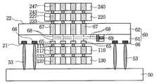
도 2를 참조하면, 본 발명의 제 1 실시 예에 따른 반도체패키지는 베이스기판(50), 로직 칩(60), 제 1 메모리칩(110), 제 2 메모리칩(220), 제 3 메모리칩(130), 및 제 4 메모리칩(240)을 포함할 수 있다.Referring to FIG. 2, the semiconductor package according to the first embodiment of the present invention may include a
상기 베이스기판(50)은 외부입출력단자들을 포함하는 인쇄회로기판 또는 반도체기판일 수 있다. 상기 로직 칩(60)은 상기 베이스기판(50) 상에 배치될 수 있다. 상기 로직 칩(60)은 제 1 표면(21) 및 상기 제 1 표면(21)과 대향하는 제 2 표면(22)을 포함할 수 있다. 상기 제 1 메모리칩(110) 및 상기 제 3 메모리칩(130)은 상기 제 1 표면(21) 상에 순차적으로 부착될 수 있다. 상기 제 2 메모리칩(220) 및 상기 제 4 메모리칩(240)은 상기 제 2 표면(22) 상에 순차적으로 부착될 수 있다. 상기 제 1 메모리칩(110) 및 상기 제 3 메모리칩(130)은 상기 베이스기판(50) 및 상기 로직 칩(60) 사이에 배치될 수 있다.The
상기 로직 칩(60)은 회로영역(61) 및 기판영역(62)으로 분류될 수 있다. 상기 회로영역(61)은 상기 기판영역(62) 상에 배치될 수 있다. 상기 회로영역(61)에 상기 제 1 표면(21)이 제공될 수 있다. 상기 기판영역(62)에 상기 제 2 표면(22)이 제공될 수 있다. 상기 제 1 표면(21)은 상기 로직 칩(60)의 전면(front surface)일 수 있으며 상기 제 2 표면(22)은 상기 로직 칩(60)의 후면(back surface)일 수 있다. 상기 제 1 표면(21)은 상기 로직 칩(60)의 상면일 수 있으며 상기 제 2 표면(22)은 상기 로직 칩(60)의 하면일 수 있다. 상기 제 1 표면(21) 및 상기 제 2 표면(22)은 서로 평행할 수 있다.The
상기 로직 칩(60)은 다수의 제 1 신호 단자(65), 다수의 제 2 신호 단자(67), 다수의 입출력 단자(66), 직병렬변환기(serializer/deserializer; SerDes; 69), 및 다수의 상호연결배선(interconnection; 68)을 포함할 수 있다. 상기 제 1 신호 단자(65), 상기 입출력 단자(66), 상기 직병렬변환기(69), 및 상기 상호연결배선(68)은 상기 회로영역(61)에 형성될 수 있다. 상기 제 2 신호 단자(67)는 상기 기판영역(62)을 관통하는 티에스브이(through silicon via; TSV)와 같은 관통 전극일 수 있다.The
상기 제 1 신호 단자(65) 및 상기 제 2 신호 단자(67)는 서로 떨어지도록 형성될 수 있다. 상기 제 1 신호 단자(65) 및 상기 제 2 신호 단자(67)는 각각 상기 상호연결배선(68)을 통하여 상기 직병렬변환기(69)에 전기적으로 접속될 수 있다. 상기 입출력 단자(66) 또한 다른 배선(도시하지 않음)을 통하여 상기 직병렬변환기(69)에 전기적으로 접속될 수 있다. 상기 제 1 신호 단자(65) 및 상기 입출력 단자(66)는 상기 제 1 표면(21)에 노출될 수 있다.The
상기 입출력 단자(66)는 도전성 볼(conductive ball), 도전성 범프(conductive bump), 도전성 와이어(conductive wire), 또는 도전성 스페이서(conductive spacer)와 같은 연결수단(53)에 의하여 상기 베이스기판(50)에 전기적으로 접속될 수 있다. 예를 들면, 상기 도전성 볼은 솔더 볼(solder ball), 골드 볼(gold ball), 실버 볼(silver ball), 또는 이들의 조합일 수 있다. 상기 도전성 범프는 솔더 범프(solder bump), 골드 범프(gold bump), 실버 범프(silver bump), 니켈 범프(Ni bump), 또는 이들의 조합일 수 있다. 상기 도전성 와이어는 골드 와이어(gold wire), 실버 와이어(silver wire), 알루미늄 와이어(aluminum wire), 또 는 이들의 조합일 수 있다. 상기 도전성 스페이서는 구리 스페이서(copper spacer), 알루미늄 스페이서(aluminum spacer), 질화티타늄 스페이서(TiN spacer), 질화탄탈룸 스페이서(TaN spacer), 골드 스페이서(gold spacer), 실버 스페이서(silver spacer), 백금 스페이서(Pt spacer), 니켈 스페이서(Ni spacer), 텅스텐 스페이서(W spacer), 또는 이들의 조합일 수 있다.The input /
상기 제 1 메모리칩(110)은 서로 떨어지도록 배치된 다수의 제 1 메모리 신호 단자(117)를 포함할 수 있으며, 상기 제 2 메모리칩(220)은 서로 떨어지도록 배치된 다수의 제 2 메모리 신호 단자(227)를 포함할 수 있고, 상기 제 3 메모리칩(130)은 서로 떨어지도록 배치된 다수의 제 3 메모리 신호 단자(137)를 포함할 수 있으며, 상기 제 4 메모리칩(240)은 서로 떨어지도록 배치된 다수의 제 4 메모리 신호 단자(247)를 포함할 수 있다. 상기 제 1 내지 제 4 메모리칩들(110, 220, 130, 240)의 각각은 다수의 메모리 셀(도시하지 않음), 상기 메모리 셀에 전기적으로 접속된 비트라인(도시하지 않음) 및 워드라인(도시하지 않음)을 포함할 수 있으나, 간략한 설명을 위하여 생략하기로 한다. 상기 메모리 셀은 상기 제 1 내지 제 4 메모리 신호 단자(117, 227, 137, 247) 중 대응하는 하나에 전기적으로 접속될 수 있다.The
상기 제 1 내지 제 4 메모리 신호 단자(117, 227, 137, 247)는 티에스브이(through silicon via; TSV)와 같은 관통 전극일 수 있다. 상기 제 1 내지 제 4 메모리 신호 단자(117, 227, 137, 247)는 구리(Cu), 티타늄(Ti), 탄탈룸(Ta), 질화티타늄(TiN), 질화탄탈룸(TaN), 니켈(Ni), 텅스텐(W), 및 이들의 조합으로 이루어 진 일군에게서 선택된 하나일 수 있다. 예를 들면, 상기 제 1 내지 제 4 메모리 신호 단자(117, 227, 137, 247)는 Ti/TiN 막일 수 있다.The first to fourth
상기 제 1 메모리 신호 단자(117) 및 상기 제 1 신호 단자(65) 사이에 제 1 도전성 범프(113)가 배치될 수 있다. 상기 제 2 메모리 신호 단자(227) 및 상기 제 2 신호 단자(67) 사이에 제 2 도전성 범프(223)가 배치될 수 있다. 상기 제 3 메모리 신호 단자(137) 및 상기 제 1 메모리 신호 단자(117) 사이에 제 3 도전성 범프(133)가 배치될 수 있다. 상기 제 4 메모리 신호 단자(247) 및 상기 제 2 메모리 신호 단자(227) 사이에 제 4 도전성 범프(243)가 배치될 수 있다. 상기 제 1 내지 제 4 도전성 범프(113, 223, 133, 243)는 솔더 범프(solder bump), 골드 범프(gold bump), 실버 범프(silver bump), 니켈 범프(Ni bump), 또는 이들의 조합일 수 있다.A first
다른 실시 예들에서 상기 제 1 내지 제 4 도전성 범프(113, 223, 133, 243)는 도전성 볼(conductive ball), 도전성 와이어(conductive wire), 또는 도전성 스페이서(conductive spacer)로 대체될 수 있다.In other embodiments, the first to fourth
이제 도 2를 다시 참조하여 본 발명의 제 1 실시 예에 따른 반도체패키지의 동작을 설명하기로 한다.Referring to FIG. 2 again, the operation of the semiconductor package according to the first embodiment of the present invention will be described.
도 2를 다시 참조하면, 상기 직병렬변환기(69)는 병렬신호를 입력받아 직렬신호 또는 병렬신호를 출력할 수 있으며, 이와 반대로, 직렬신호를 입력받아 병렬신호 또는 직렬신호를 출력하는 역할을 할 수 있다.Referring to FIG. 2 again, the serial-to-
상술한 바와 같이, 상기 직병렬변환기(69)는 상기 상호연결배선(68), 상기 제 1 신호 단자(65), 상기 제 1 도전성 범프(113) 및 상기 제 1 메모리 신호 단자(117)를 통하여 상기 제 1 메모리칩(110)에 내장된 메모리 셀과 전기적으로 접속될 수 있다. 또한, 상기 직병렬변환기(69)는 상기 상호연결배선(68), 상기 제 2 신호 단자(67), 상기 제 2 도전성 범프(223) 및 상기 제 2 메모리 신호 단자(227)를 통하여 상기 제 2 메모리칩(220)에 내장된 메모리 셀과 전기적으로 접속될 수 있다. 즉, 상기 제 1 메모리칩(110)에 내장된 메모리 셀 및 상기 제 2 메모리칩(220)에 내장된 메모리 셀은 상기 직병렬변환기(69)에 병렬접속될 수 있다.As described above, the serial-to-
이에 따라, 상기 제 1 메모리칩(110)에 저장된 데이터 및 상기 제 2 메모리칩(220)에 저장된 데이터는 상기 직병렬변환기(69)에 병렬접속될 수 있다. 이 경우에, 상기 직병렬변환기(69)는 상기 제 1 메모리칩(110) 및 상기 제 2 메모리칩(220)에 저장된 데이터들을 동시에 읽어내고 상기 입출력 단자들(66) 및 상기 베이스기판(50)을 경유하여 외부로 출력할 수 있다. 이와 마찬가지로, 상기 직병렬변환기(69)는 상기 입출력 단자들(66)을 통하여 외부로부터 입력된 데이터들을 상기 제 1 메모리칩(110) 및 상기 제 2 메모리칩(220)에 분배하는 역할을 병렬 수행할 수 있다. 즉, 상기 제 1 메모리칩(110) 및 상기 제 2 메모리칩(220)이 상기 직병렬변환기(69)에 직렬접속된 경우에 비하여 상대적으로 빠른 입출력특성을 보일 수 있다.Accordingly, the data stored in the
이에 더하여, 상기 직병렬변환기(69)는 상기 상호연결배선(68), 상기 제 1 신호 단자(65), 상기 제 1 도전성 범프(113), 상기 제 1 메모리 신호 단자(117), 상기 제 3 도전성 범프(133), 및 상기 제 3 메모리 신호 단자(137)를 통하여 상기 제 3 메모리칩(130)에 내장된 메모리 셀과 전기적으로 접속될 수 있다. 이 경우에, 상기 제 1 메모리 신호 단자(117) 및 상기 제 3 메모리 신호 단자(137)는 직렬접속될 수 있다. 또한, 상기 직병렬변환기(69)는 상기 상호연결배선(68), 상기 제 2 신호 단자(67), 상기 제 2 도전성 범프(223), 상기 제 2 메모리 신호 단자(227), 상기 제 4 도전성 범들(243), 및 상기 제 4 메모리 신호 단자(247)를 통하여 상기 제 4 메모리칩(240)에 내장된 메모리 셀과 전기적으로 접속될 수 있다.In addition, the serial-to-
즉, 상기 제 1 메모리칩(110) 및 상기 제 3 메모리칩(130)에 내장된 메모리 셀들은 상기 제 1 신호 단자(65)를 통하여 상기 직병렬변환기(69)에 직렬접속될 수 있으며, 상기 제 2 메모리칩(220) 및 상기 제 4 메모리칩(240)에 내장된 메모리 셀들은 상기 제 2 신호 단자(67)를 통하여 상기 직병렬변환기(69)에 직렬접속될 수 있다. 이에 따라, 상기 제 1 내지 제 4 메모리칩들(110, 220, 130, 240)이 모두 상기 직병렬변환기(69)에 직렬접속된 경우에 비하여 상대적으로 빠른 입출력특성을 보일 수 있다.That is, the memory cells embedded in the
도 3을 참조하면, 본 발명의 제 2 실시 예에 따른 반도체패키지는 베이스기판(50), 로직 칩(60), 제 1 메모리칩(110), 제 2 메모리칩(220), 제 3 메모리칩(130), 제 4 메모리칩(240), 제 5 메모리칩(150), 및 제 6 메모리칩(260)을 구비할 수 있다. 이에 더하여, 상기 제 3 메모리칩(130) 및 상기 제 5 메모리칩(150) 사이에 하나 이상의 다른 메모리칩들이 배치될 수 있다. 더 나아가서, 상기 제 4 메모리칩(240) 및 상기 제 6 메모리칩(260) 사이에 하나 이상의 또 다른 메모리칩들이 배치될 수 있다. 이하에서는 본 발명의 제 1 실시 예와의 차이점만 간략하게 설명하기로 한다.Referring to FIG. 3, the semiconductor package according to the second embodiment of the present invention may include a
상기 베이스기판(50)은 외부입출력단자들을 구비하는 인쇄회로기판 또는 반도체기판일 수 있다. 상기 로직 칩(60)은 상기 베이스기판(50) 상에 배치될 수 있다. 상기 로직 칩(60)은 제 1 표면(21) 및 상기 제 1 표면(21)과 마주보는 제 2 표면(22)을 구비할 수 있다. 상기 제 1 메모리칩(110), 상기 제 3 메모리칩(130), 및 상기 제 5 메모리칩(150)은 상기 제 1 표면(21) 상에 순차적으로 부착될 수 있다. 상기 제 2 메모리칩(220), 상기 제 4 메모리칩(240), 및 상기 제 6 메모리칩(260)은 상기 제 2 표면(22) 상에 순차적으로 부착될 수 있다. 상기 제 1 메모리칩(110), 상기 제 3 메모리칩(130), 및 상기 제 5 메모리칩(150)은 상기 베이스기판(50) 및 상기 로직 칩(60) 사이에 배치될 수 있다.The
상기 로직 칩(60)은 회로영역(61) 및 기판영역(62)으로 분류될 수 있다. 상기 회로영역(61)에 상기 제 1 표면(21)이 제공될 수 있다. 상기 기판영역(62)에 상기 제 2 표면(22)이 제공될 수 있다.The
상기 로직 칩(60)은 다수의 제 1 신호 단자(65), 다수의 제 2 신호 단자(67), 다수의 입출력 단자(66), 직병렬변환기(serializer/deserializer; SerDes; 69), 및 다수의 상호연결배선(interconnection; 68)을 구비할 수 있다. 상기 제 1 신호 단자(65), 상기 입출력 단자(66), 상기 직병렬변환기(69), 및 상기 상호연결배선(68)은 상기 회로영역(61)에 배치될 수 있다. 상기 제 2 신호 단자(67)는 상기 기판영역(62)을 관통하는 티에스브이(through silicon via; TSV)와 같은 관통 전극일 수 있다.The
상기 제 1 신호 단자(65) 및 상기 제 2 신호 단자(67)는 서로 떨어지도록 배치될 수 있다. 상기 제 1 신호 단자(65) 및 상기 제 2 신호 단자(67)는 각각 상기 상호연결배선(68)을 통하여 상기 직병렬변환기(69)에 전기적으로 접속될 수 있다. 상기 입출력 단자(66) 또한 다른 배선(도시하지 않음)을 통하여 상기 직병렬변환기(69)에 전기적으로 접속될 수 있다. 상기 제 1 신호 단자(65) 및 상기 입출력 단자(66)는 상기 제 1 표면(21)에 노출될 수 있다.The
상기 제 5 메모리칩(150)은 서로 떨어지도록 배치된 다수의 제 5 메모리 신호 단자(157)를 구비할 수 있으며, 상기 제 6 메모리칩(260)은 서로 떨어지도록 배치된 다수의 제 6 메모리 신호 단자(267)를 구비할 수 있다. 상기 제 1 내지 제 6 메모리칩(110, 220, 130, 240, 150, 260)은 다수의 메모리 셀(도시하지 않음), 상기 메모리 셀에 전기적으로 접속된 비트라인(도시하지 않음) 및 워드라인(도시하지 않음)을 구비할 수 있으나, 간략한 설명을 위하여 생략하기로 한다. 상기 메모리 셀은 상기 제 1 내지 제 6 메모리 신호 단자(117, 227, 137, 247, 157, 267) 중 대응하는 하나에 전기적으로 접속될 수 있다.The
상기 제 1 내지 제 6 메모리 신호 단자(117, 227, 137, 247, 157, 267)는 티에스브이(through silicon via; TSV)와 같은 관통 전극일 수 있다. 상기 제 1 내지 제 6 메모리 신호 단자(117, 227, 137, 247, 157, 267)는 구리(Cu), 티타늄(Ti), 탄탈룸(Ta), 질화티타늄(TiN), 질화탄탈룸(TaN), 니켈(Ni), 텅스텐(W), 및 이들의 조합으로 이루어진 일군에게서 선택된 하나일 수 있다. 예를 들면, 상기 제 1 내지 제 6 메모리 신호 단자(117, 227, 137, 247, 157, 267)는 Ti/TiN 막일 수 있다.The first to sixth
상기 제 3 메모리 신호 단자(137) 및 상기 제 5 메모리 신호 단자(137) 사이에 제 5 도전성 범프(153)가 배치될 수 있다. 상기 제 4 메모리 신호 단자(247) 및 상기 제 6 메모리 신호 단자(267) 사이에 제 6 도전성 범프(263)가 배치될 수 있다. 상기 제 1 내지 제 6 도전성 범프(113, 223, 133, 243, 153, 263)는 솔더 범프(solder bump), 골드 범프(gold bump), 실버 범프(silver bump), 니켈 범프(Ni bump), 또는 이들의 조합일 수 있다.A fifth
다른 실시 예들에서, 상기 제 1 내지 제 6 도전성 범프(113, 223, 133, 243, 153, 263)는 도전성 볼(conductive ball), 도전성 와이어(conductive wire), 또는 도전성 스페이서(conductive spacer)로 대체될 수 있다.In other embodiments, the first to sixth
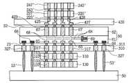
도 4를 참조하면, 본 발명의 제 3 실시 예에 따른 반도체패키지는 베이스기판(50), 로직 칩(60), 제 1 메모리칩(110), 제 2 메모리칩(220), 제 3 메모리칩(130), 및 제 4 메모리칩(240)을 구비할 수 있다. 이하에서는 본 발명의 제 1 실시 예와의 차이점만 간략하게 설명하기로 한다.Referring to FIG. 4, the semiconductor package according to the third embodiment of the present invention may include a
상기 베이스기판(50)은 외부입출력단자들을 구비하는 인쇄회로기판 또는 반도체기판일 수 있다. 상기 로직 칩(60)은 상기 베이스기판(50) 상에 배치될 수 있다. 상기 로직 칩(60)은 제 1 표면(21) 및 상기 제 1 표면(21)과 마주보는 제 2 표면(22)을 구비할 수 있다. 상기 제 1 메모리칩(110) 및 상기 제 3 메모리칩(130)은 상기 제 1 표면(21) 상에 순차적으로 부착될 수 있다. 상기 제 2 메모리칩(220) 및 상기 제 4 메모리칩(240)은 상기 제 2 표면(22) 상에 순차적으로 부착될 수 있다. 상기 제 1 메모리칩(110) 및 상기 제 3 메모리칩(130)은 상기 베이스기판(50) 및 상기 로직 칩(60) 사이에 배치될 수 있다.The
상기 로직 칩(60)은 회로영역(61) 및 기판영역(62)으로 분류될 수 있다. 상기 회로영역(61)은 상기 기판영역(62) 상에 배치될 수 있다. 상기 회로영역(61)에 상기 제 1 표면(21)이 제공될 수 있다. 상기 기판영역(62)에 상기 제 2 표면(22)이 제공될 수 있다. 상기 제 1 표면(21)은 상기 로직 칩(60)의 전면(front surface)일 수 있으며 상기 제 2 표면(22)은 상기 로직 칩(60)의 후면(back surface)일 수 있다.The
상기 로직 칩(60)은 다수의 제 1 신호 단자(65'), 다수의 제 2 신호 단자(67'), 다수의 입출력 단자(66), 직병렬변환기(serializer/deserializer; SerDes; 69), 및 다수의 상호연결배선(interconnection; 68)을 구비할 수 있다. 상기 제 1 신호 단자(65'), 상기 입출력 단자(66), 상기 직병렬변환기(69), 및 상기 상호연결배선(68)은 상기 회로영역(61)에 배치될 수 있다. 상기 제 2 신호 단자(67')는 상기 기판영역(62) 및 상기 회로영역(61)을 관통하는 티에스브이(through silicon via; TSV)와 같은 관통 전극일 수 있다.The
상기 제 1 신호 단자(65') 및 상기 제 2 신호 단자(67')는 서로 떨어지도록 배치될 수 있다. 상기 제 1 신호 단자(65') 및 상기 제 2 신호 단자(67')는 각각 상기 상호연결배선(68)을 통하여 상기 직병렬변환기(69)에 전기적으로 접속될 수 있다. 상기 입출력 단자(66) 또한 다른 배선(도시하지 않음)을 통하여 상기 직병렬변환기(69)에 전기적으로 접속될 수 있다. 상기 제 1 신호 단자(65') 및 상기 입출력 단자(66)는 상기 제 1 표면(21)에 노출될 수 있다.The
상기 입출력 단자들(66)의 각각은 도전성 볼(conductive ball), 도전성 범프(conductive bump), 도전성 와이어(conductive wire), 또는 도전성 스페이서(conductive spacer)와 같은 연결수단들(53)에 의하여 상기 베이스기판(50)에 전기적으로 접속될 수 있다.Each of the input /
상기 제 1 메모리칩(110)은 서로 떨어지도록 배치된 다수의 제 1 메모리 신호 단자(117)를 구비할 수 있으며, 상기 제 2 메모리칩(220)은 서로 떨어지도록 배치된 다수의 제 2 메모리 신호 단자(227)를 구비할 수 있고, 상기 제 3 메모리칩(130)은 서로 떨어지도록 배치된 다수의 제 3 메모리 신호 단자(137)를 구비할 수 있으며, 상기 제 4 메모리칩(240)은 서로 떨어지도록 배치된 다수의 제 4 메모리 신호 단자(247)를 구비할 수 있다. 상기 제 1 내지 제 4 메모리칩(110, 220, 130, 240)은 다수의 메모리 셀(도시하지 않음), 상기 메모리 셀에 전기적으로 접속된 비트라인(도시하지 않음) 및 워드라인(도시하지 않음)을 구비할 수 있으나, 간략한 설명을 위하여 생략하기로 한다. 상기 메모리 셀은 상기 제 1 내지 제 4 메모리 신호 단자(117, 227, 137, 247) 중 대응하는 하나에 전기적으로 접속될 수 있다.The
상기 제 1 메모리 신호 단자(117) 및 상기 제 1 신호 단자(65') 사이에 제 1 도전성 범프(113)가 배치될 수 있다. 상기 제 2 메모리 신호 단자(227) 및 상기 제 2 신호 단자(67') 사이에 제 2 도전성 범프(223)가 배치될 수 있다. 이 경우에, 상기 제 1 메모리칩(110) 및 상기 제 2 메모리칩(220)은 서로 어긋나게 배치될 수 있다. 상기 제 3 메모리 신호 단자(137) 및 상기 제 1 메모리 신호 단자(117) 사이에 제 3 도전성 범프(133)가 배치될 수 있다. 상기 제 4 메모리 신호 단자(247) 및 상기 제 2 메모리 신호 단자(227) 사이에 제 4 도전성 범프(243)가 배치될 수 있다. 상기 제 1 내지 제 4 도전성 범프(113, 223, 133, 243)는 솔더 범프(solder bump), 골드 범프(gold bump), 실버 범프(silver bump), 니켈 범프(Ni bump), 또는 이들의 조합일 수 있다.A first
다른 실시 예들에서 상기 제 1 내지 제 4 도전성 범프(113, 223, 133, 243)는 도전성 볼(conductive ball), 도전성 와이어(conductive wire), 또는 도전성 스페이서(conductive spacer)로 대체될 수 있다.In other embodiments, the first to fourth
도 5를 참조하면, 본 발명의 제 4 실시 예에 따른 반도체패키지는 베이스기판(50), 로직 칩(60), 제 1 메모리칩(110), 제 2 메모리칩(220), 제 3 메모리칩(130), 제 4 메모리칩(240), 제 1 인터포저(first interposer; 310) 및 제 2 인터포저(second interposer; 420)를 구비할 수 있다.Referring to FIG. 5, the semiconductor package according to the fourth embodiment of the present invention may include a
상기 베이스기판(50)은 외부입출력단자들을 구비하는 인쇄회로기판 또는 반도체기판일 수 있다. 상기 로직 칩(60)은 상기 베이스기판(50) 상에 배치될 수 있다. 상기 로직 칩(60)은 제 1 표면(21) 및 상기 제 1 표면(21)과 마주보는 제 2 표면(22)을 구비할 수 있다. 상기 제 1 메모리칩(110) 및 상기 제 3 메모리칩(130)은 상기 제 1 표면(21) 상에 순차적으로 부착될 수 있다. 상기 제 2 메모리칩(220) 및 상기 제 4 메모리칩(240)은 상기 제 2 표면(22) 상에 순차적으로 부착될 수 있다. 상기 제 1 메모리칩(110) 및 상기 제 3 메모리칩(130)은 상기 베이스기판(50) 및 상기 로직 칩(60) 사이에 배치될 수 있다.The
상기 제 1 인터포저(310)는 상기 로직 칩(60) 및 상기 제 1 메모리칩(110) 사이에 배치될 수 있다. 즉, 상기 제 1 인터포저(310)는 상기 제 1 표면(21) 상에 부착될 수 있다. 상기 제 2 인터포저(420)는 상기 로직 칩(60) 및 상기 제 2 메모리칩(220) 사이에 배치될 수 있다. 즉, 상기 제 2 인터포저(420)는 상기 제 2 표면(22) 상에 부착될 수 있다.The
상기 로직 칩(60)은 회로영역(61) 및 기판영역(62)으로 분류될 수 있다. 상기 회로영역(61)은 상기 기판영역(62) 상에 배치될 수 있다. 상기 회로영역(61)에 상기 제 1 표면(21)이 제공될 수 있다. 상기 기판영역(62)에 상기 제 2 표면(22)이 제공될 수 있다. 상기 제 1 표면(21)은 상기 로직 칩(60)의 전면(front surface)일 수 있으며 상기 제 2 표면(22)은 상기 로직 칩(60)의 후면(back surface)일 수 있다.The
상기 로직 칩(60)은 다수의 제 1 신호 단자(65), 다수의 제 2 신호 단자(67), 다수의 입출력 단자(66), 직병렬변환기(serializer/deserializer; SerDes; 69), 및 다수의 상호연결배선(interconnection; 68)을 구비할 수 있다. 상기 제 1 신호 단자(65), 상기 입출력 단자(66), 상기 직병렬변환기(69), 및 상기 상호연결배선(68)은 상기 회로영역(61)에 배치될 수 있다. 상기 제 2 신호 단자(67)는 상기 기판영역(62)을 관통하는 티에스브이(through silicon via; TSV)와 같은 관통 전극일 수 있다.The
상기 제 1 신호 단자(65) 및 상기 제 2 신호 단자(67)는 서로 떨어지도록 배치될 수 있다. 상기 제 1 신호 단자(65) 및 상기 제 2 신호 단자(67)는 각각 상기 상호연결배선(68)을 통하여 상기 직병렬변환기(69)에 전기적으로 접속될 수 있다. 상기 입출력 단자(66) 또한 다른 배선(도시하지 않음)을 통하여 상기 직병렬변환기(69)에 전기적으로 접속될 수 있다. 상기 제 1 신호 단자(65) 및 상기 입출력 단자(66)는 상기 제 1 표면(21)에 노출될 수 있다.The
상기 제 1 인터포저(310) 및 상기 제 2 인터포저(420)는 재배선 층의 역할을 할 수 있다. 상기 제 1 인터포저(310)는 다수의 제 1 재배선 단자(317) 및 다수의 입출력 관통 전극(327)을 구비할 수 있다. 상기 제 1 재배선 단자들(317)은 티에스브이(through silicon via; TSV)와 같은 관통 전극일 수 있다. 상기 제 1 재배선 단자들(317)은 상기 제 1 신호 단자들(65)에 대응하는 크기 및 간격을 구비하도록 배치된 것일 수 있다. 상기 입출력 관통 전극(327)은 상기 입출력 단자(66)에 대응하는 크기 및 간격을 구비하도록 배치된 것일 수 있다.The
상기 제 2 인터포저(420)의 일면에 다수의 제 2 재배선 단자(427)가 제공될 수 있다. 상기 제 2 재배선 단자(427)는 상기 제 2 신호 단자(67)에 대응하는 크기 및 간격을 구비하도록 배치된 것일 수 있다. 상기 제 2 인터포저(420)의 다른 일면에 다수의 제 3 재배선 단자(428)가 제공될 수 있다. 상기 제 3 재배선 단자(428)는 인터포저 배선(425)을 통하여 상기 제 2 재배선 단자(427) 중 대응하는 하나에 전기적으로 접속될 수 있다.A plurality of
상기 제 1 재배선 단자(317), 상기 입출력 관통 전극(327), 상기 제 2 재배선 단자(427), 상기 제 3 재배선 단자(428) 및 상기 인터포저 배선(425)은 구리(Cu), 티타늄(Ti), 탄탈룸(Ta), 질화티타늄(TiN), 질화탄탈룸(TaN), 니켈(Ni), 텅스텐(W), 및 이들의 조합으로 이루어진 일군에게서 선택된 하나일 수 있다.The
상기 제 1 재배선 단자(317) 및 상기 제 1 신호 단자(65) 사이에 제 1 재배선 범프(313)가 배치될 수 있다. 또한, 상기 입출력 관통 전극(327) 및 상기 입출력 단자(66) 사이에도 상기 제 1 재배선 범프(313)가 배치될 수 있다. 상기 제 2 재배선 단자(427) 및 상기 제 2 신호 단자(67) 사이에 제 2 재배선 범프(423)가 배치될 수 있다. 상기 제 1 재배선 범프(313) 및 상기 제 2 재배선 범프(423)는 솔더 범프(solder bump), 골드 범프(gold bump), 실버 범프(silver bump), 니켈 범프(Ni bump), 또는 이들의 조합일 수 있다.A
다른 실시 예들에서 상기 제 1 재배선 범프(313) 및 상기 제 2 재배선 범프(423)는 도전성 볼(conductive ball), 도전성 와이어(conductive wire), 또는 도전성 스페이서(conductive spacer)로 대체될 수 있다.In other embodiments, the
상기 입출력 관통 전극(327)은 도전성 볼(conductive ball), 도전성 범프(conductive bump), 도전성 와이어(conductive wire), 또는 도전성 스페이서(conductive spacer)와 같은 연결수단들(53')에 의하여 상기 베이스기판(50)에 전기적으로 접속될 수 있다. 예를 들면, 상기 도전성 볼은 솔더 볼(solder ball), 골드 볼(gold ball), 실버 볼(silver ball), 또는 이들의 조합일 수 있다. 상기 도전성 범프는 솔더 범프(solder bump), 골드 범프(gold bump), 실버 범프(silver bump), 니켈 범프(Ni bump), 또는 이들의 조합일 수 있다. 상기 도전성 와이어는 골드 와이어(gold wire), 실버 와이어(silver wire), 알루미늄 와이어(aluminum wire), 또는 이들의 조합일 수 있다. 상기 도전성 스페이서는 구리 스페이 서(copper spacer), 알루미늄 스페이서(aluminum spacer), 질화티타늄 스페이서(TiN spacer), 질화탄탈룸 스페이서(TaN spacer), 골드 스페이서(gold spacer), 실버 스페이서(silver spacer), 백금 스페이서(Pt spacer), 니켈 스페이서(Ni spacer), 텅스텐 스페이서(W spacer), 또는 이들의 조합일 수 있다.The input / output through
상기 제 1 메모리칩(110)은 서로 떨어지도록 배치된 다수의 제 1 메모리 신호 단자(117)를 구비할 수 있으며, 상기 제 2 메모리칩(220')은 서로 떨어지도록 배치된 다수의 제 2 메모리 신호 단자(227')를 구비할 수 있고, 상기 제 3 메모리칩(130)은 서로 떨어지도록 배치된 다수의 제 3 메모리 신호 단자(137)를 구비할 수 있으며, 상기 제 4 메모리칩(240')은 서로 떨어지도록 배치된 다수의 제 4 메모리 신호 단자(247')를 구비할 수 있다.The
상기 제 1 메모리칩(110) 및 상기 제 2 메모리칩(220')은 서로 다른 규격을 갖는 것일 수 있다. 예를 들면, 상기 제 2 메모리칩(220')은 상기 제 1 메모리칩(110)의 축소판(shrink version)일 수 있다. 상기 제 3 메모리칩(130)은 상기 제 1 메모리칩(110)과 동일한 규격을 갖는 것일 수 있다. 또한, 상기 제 4 메모리칩(240')은 상기 제 2 메모리칩(220')과 동일한 규격을 갖는 것일 수 있다.The
상기 제 1 내지 제 4 메모리칩들(110, 220', 130, 240')의 각각은 다수의 메모리 셀(도시하지 않음), 상기 메모리 셀에 전기적으로 접속된 비트라인(도시하지 않음) 및 워드라인(도시하지 않음)을 구비할 수 있으나, 간략한 설명을 위하여 생략하기로 한다. 상기 메모리 셀은 상기 제 1 내지 제 4 메모리 신호 단자(117, 227', 137, 247') 중 대응하는 하나에 전기적으로 접속될 수 있다.Each of the first to
상기 제 1 내지 제 4 메모리 신호 단자(117, 227', 137, 247')는 티에스브이(through silicon via; TSV)와 같은 관통 전극일 수 있다. 상기 제 1 내지 제 4 메모리 신호 단자(117, 227', 137, 247')는 구리(Cu), 티타늄(Ti), 탄탈룸(Ta), 질화티타늄(TiN), 질화탄탈룸(TaN), 니켈(Ni), 텅스텐(W), 및 이들의 조합으로 이루어진 일군에게서 선택된 하나일 수 있다. 예를 들면, 상기 제 1 내지 제 4 메모리 신호 단자(117, 227', 137, 247')는 Ti/TiN 막일 수 있다.The first to fourth
상기 제 1 메모리 신호 단자(117)은 상기 제 1 재배선 단자(317)에 대응하는 크기 및 간격을 구비하도록 배치된 것일 수 있다. 상기 제 1 메모리 신호 단자(117) 및 상기 제 1 재배선 단자(317) 사이에 제 1 도전성 범프(113)가 배치될 수 있다. 상기 제 2 메모리 신호 단자(227')는 상기 제 3 재배선 단자(428)에 대응하는 크기 및 간격을 구비하도록 배치된 것일 수 있다. 상기 제 2 메모리 신호 단자(227') 및 상기 제 3 재배선 단자(428) 사이에 제 2 도전성 범프(223')가 배치될 수 있다. 상기 제 3 메모리 신호 단자(137) 및 상기 제 1 메모리 신호 단자(117) 사이에 제 3 도전성 범프(133)가 배치될 수 있다. 상기 제 4 메모리 신호 단자(247') 및 상기 제 2 메모리 신호 단자(227') 사이에 제 4 도전성 범프(243')가 배치될 수 있다. 상기 제 1 내지 제 4 도전성 범프(113, 223', 133, 243')는 솔더 범프(solder bump), 골드 범프(gold bump), 실버 범프(silver bump), 니켈 범프(Ni bump), 또는 이들의 조합일 수 있다.The first
다른 실시 예들에서 상기 제 1 내지 제 4 도전성 범프(113, 223', 133, 243')는 도전성 볼(conductive ball), 도전성 와이어(conductive wire), 또는 도전 성 스페이서(conductive spacer)로 대체될 수 있다.In other embodiments, the first to fourth
도 4에 도시된 바와 같이, 상기 제 1 인터포저(310) 및 상기 제 2 인터포저(420)를 이용하여 서로 다른 크기를 갖는 상기 제 1 메모리칩(110) 및 상기 제 2 메모리칩(220')을 상기 로직 칩(60)에 병렬접속할 수 있다.As shown in FIG. 4, the
본 발명은 상술한 실시 예들에 한정되지 않고 본 발명의 사상 내에서 여러 가지의 다른 형태로 변형될 수 있다. 예를 들면, 상기 메모리칩들(110, 220, 130, 240, 150, 260)은 반도체칩(semiconductor chip), 반도체 메모리코아(semiconductor memory core), 반도체 메모리패키지(semiconductor memory package), 또는 이들의 조합과 같은 다른 반도체장치로 대체될 수 있다.The present invention is not limited to the above-described embodiments and can be modified in various other forms within the spirit of the present invention. For example, the
도 1은 종래기술에 의한 복수의 메모리칩들을 구비하는 반도체패키지를 보여주는 개략도이다.1 is a schematic view showing a semiconductor package having a plurality of memory chips according to the prior art.
도 2 내지 도 5는 본 발명의 제 1 내지 제 4 실시 예들에 따른 로직 칩에 층층이 쌓인 메모리칩들을 구비하는 반도체패키지를 설명하기 위한 단면도들이다.2 to 5 are cross-sectional views illustrating a semiconductor package including memory chips stacked with layers in a logic chip according to the first to fourth embodiments of the present invention.
Claims (20)
Translated fromKoreanPriority Applications (3)
| Application Number | Priority Date | Filing Date | Title |
|---|---|---|---|
| KR1020070083607AKR101213175B1 (en) | 2007-08-20 | 2007-08-20 | Semiconductor package having memory devices stacked on logic chip |
| US12/190,224US7834450B2 (en) | 2007-08-20 | 2008-08-12 | Semiconductor package having memory devices stacked on logic device |
| US12/946,141US8253244B2 (en) | 2007-08-20 | 2010-11-15 | Semiconductor package having memory devices stacked on logic device |
Applications Claiming Priority (1)
| Application Number | Priority Date | Filing Date | Title |
|---|---|---|---|
| KR1020070083607AKR101213175B1 (en) | 2007-08-20 | 2007-08-20 | Semiconductor package having memory devices stacked on logic chip |
Publications (2)
| Publication Number | Publication Date |
|---|---|
| KR20090019297A KR20090019297A (en) | 2009-02-25 |
| KR101213175B1true KR101213175B1 (en) | 2012-12-18 |
Family
ID=40381978
Family Applications (1)
| Application Number | Title | Priority Date | Filing Date |
|---|---|---|---|
| KR1020070083607AActiveKR101213175B1 (en) | 2007-08-20 | 2007-08-20 | Semiconductor package having memory devices stacked on logic chip |
Country Status (2)
| Country | Link |
|---|---|
| US (2) | US7834450B2 (en) |
| KR (1) | KR101213175B1 (en) |
Cited By (1)
| Publication number | Priority date | Publication date | Assignee | Title |
|---|---|---|---|---|
| US10199079B2 (en) | 2017-02-21 | 2019-02-05 | SK Hynix Inc. | Semiconductor memory device |
Families Citing this family (189)
| Publication number | Priority date | Publication date | Assignee | Title |
|---|---|---|---|---|
| SG130055A1 (en) | 2005-08-19 | 2007-03-20 | Micron Technology Inc | Microelectronic devices, stacked microelectronic devices, and methods for manufacturing microelectronic devices |
| US8569876B2 (en) | 2006-11-22 | 2013-10-29 | Tessera, Inc. | Packaged semiconductor chips with array |
| US7691668B2 (en)* | 2006-12-19 | 2010-04-06 | Spansion Llc | Method and apparatus for multi-chip packaging |
| US8405196B2 (en) | 2007-03-05 | 2013-03-26 | DigitalOptics Corporation Europe Limited | Chips having rear contacts connected by through vias to front contacts |
| US8232183B2 (en)* | 2007-05-04 | 2012-07-31 | Taiwan Semiconductor Manufacturing Company, Ltd. | Process and apparatus for wafer-level flip-chip assembly |
| WO2009017835A2 (en) | 2007-07-31 | 2009-02-05 | Tessera, Inc. | Semiconductor packaging process using through silicon vias |
| KR101213175B1 (en)* | 2007-08-20 | 2012-12-18 | 삼성전자주식회사 | Semiconductor package having memory devices stacked on logic chip |
| US8492263B2 (en)* | 2007-11-16 | 2013-07-23 | Taiwan Semiconductor Manufacturing Company, Ltd. | Protected solder ball joints in wafer level chip-scale packaging |
| US8334170B2 (en)* | 2008-06-27 | 2012-12-18 | Taiwan Semiconductor Manufacturing Company, Ltd. | Method for stacking devices |
| US7851346B2 (en)* | 2008-07-21 | 2010-12-14 | Taiwan Semiconductor Manufacturing Company, Ltd. | Bonding metallurgy for three-dimensional interconnect |
| KR100915832B1 (en) | 2008-08-08 | 2009-09-07 | 주식회사 하이닉스반도체 | Read operation control circuit of semiconductor memory device |
| US8634245B2 (en) | 2008-08-08 | 2014-01-21 | Hynix Semiconductor Inc. | Control circuit of read operation for semiconductor memory apparatus |
| US8932906B2 (en) | 2008-08-19 | 2015-01-13 | Taiwan Semiconductor Manufacturing Company, Ltd. | Through silicon via bonding structure |
| US8399336B2 (en) | 2008-08-19 | 2013-03-19 | International Business Machines Corporation | Method for fabricating a 3D integrated circuit device having lower-cost active circuitry layers stacked before higher-cost active circuitry layer |
| US8334599B2 (en)* | 2008-08-21 | 2012-12-18 | Qimonda Ag | Electronic device having a chip stack |
| US8014166B2 (en)* | 2008-09-06 | 2011-09-06 | Broadpak Corporation | Stacking integrated circuits containing serializer and deserializer blocks using through silicon via |
| US9524945B2 (en) | 2010-05-18 | 2016-12-20 | Taiwan Semiconductor Manufacturing Company, Ltd. | Cu pillar bump with L-shaped non-metal sidewall protection structure |
| KR20100046760A (en) | 2008-10-28 | 2010-05-07 | 삼성전자주식회사 | Semiconductor package |
| US7943421B2 (en)* | 2008-12-05 | 2011-05-17 | Taiwan Semiconductor Manufacturing Company, Ltd. | Component stacking using pre-formed adhesive films |
| US9117828B2 (en)* | 2009-03-27 | 2015-08-25 | Taiwan Semiconductor Manufacturing Company, Ltd. | Method of handling a thin wafer |
| US8552563B2 (en)* | 2009-04-07 | 2013-10-08 | Taiwan Semiconductor Manufacturing Company, Ltd. | Three-dimensional semiconductor architecture |
| US8841766B2 (en) | 2009-07-30 | 2014-09-23 | Taiwan Semiconductor Manufacturing Company, Ltd. | Cu pillar bump with non-metal sidewall protection structure |
| US8377816B2 (en) | 2009-07-30 | 2013-02-19 | Taiwan Semiconductor Manufacturing Company, Ltd. | Method of forming electrical connections |
| US8324738B2 (en) | 2009-09-01 | 2012-12-04 | Taiwan Semiconductor Manufacturing Company, Ltd. | Self-aligned protection layer for copper post structure |
| US8803332B2 (en)* | 2009-09-11 | 2014-08-12 | Taiwan Semiconductor Manufacturing Company, Ltd. | Delamination resistance of stacked dies in die saw |
| US8659155B2 (en) | 2009-11-05 | 2014-02-25 | Taiwan Semiconductor Manufacturing Company, Ltd. | Mechanisms for forming copper pillar bumps |
| US8299616B2 (en)* | 2010-01-29 | 2012-10-30 | Taiwan Semiconductor Manufacturing Company, Ltd. | T-shaped post for semiconductor devices |
| US10297550B2 (en) | 2010-02-05 | 2019-05-21 | Taiwan Semiconductor Manufacturing Company, Ltd. | 3D IC architecture with interposer and interconnect structure for bonding dies |
| US8610270B2 (en) | 2010-02-09 | 2013-12-17 | Taiwan Semiconductor Manufacturing Company, Ltd. | Semiconductor device and semiconductor assembly with lead-free solder |
| US8803319B2 (en) | 2010-02-11 | 2014-08-12 | Taiwan Semiconductor Manufacturing Company, Ltd. | Pillar structure having a non-planar surface for semiconductor devices |
| US8318596B2 (en) | 2010-02-11 | 2012-11-27 | Taiwan Semiconductor Manufacturing Company, Ltd. | Pillar structure having a non-planar surface for semiconductor devices |
| US9385095B2 (en) | 2010-02-26 | 2016-07-05 | Taiwan Semiconductor Manufacturing Company, Ltd. | 3D semiconductor package interposer with die cavity |
| US8519537B2 (en) | 2010-02-26 | 2013-08-27 | Taiwan Semiconductor Manufacturing Company, Ltd. | 3D semiconductor package interposer with die cavity |
| US8378480B2 (en)* | 2010-03-04 | 2013-02-19 | Taiwan Semiconductor Manufacturing Company, Ltd. | Dummy wafers in 3DIC package assemblies |
| US8455995B2 (en) | 2010-04-16 | 2013-06-04 | Taiwan Semiconductor Manufacturing Company, Ltd. | TSVs with different sizes in interposers for bonding dies |
| WO2011139496A2 (en) | 2010-04-26 | 2011-11-10 | Rambus Inc. | Techniques for interconnecting stacked dies using connection sites |
| US8441124B2 (en) | 2010-04-29 | 2013-05-14 | Taiwan Semiconductor Manufacturing Company, Ltd. | Cu pillar bump with non-metal sidewall protection structure |
| US8716867B2 (en) | 2010-05-12 | 2014-05-06 | Taiwan Semiconductor Manufacturing Company, Ltd. | Forming interconnect structures using pre-ink-printed sheets |
| US8674513B2 (en) | 2010-05-13 | 2014-03-18 | Taiwan Semiconductor Manufacturing Company, Ltd. | Interconnect structures for substrate |
| US9142533B2 (en) | 2010-05-20 | 2015-09-22 | Taiwan Semiconductor Manufacturing Company, Ltd. | Substrate interconnections having different sizes |
| US8901736B2 (en) | 2010-05-28 | 2014-12-02 | Taiwan Semiconductor Manufacturing Company, Ltd. | Strength of micro-bump joints |
| US9018758B2 (en) | 2010-06-02 | 2015-04-28 | Taiwan Semiconductor Manufacturing Company, Ltd. | Cu pillar bump with non-metal sidewall spacer and metal top cap |
| US8426961B2 (en) | 2010-06-25 | 2013-04-23 | Taiwan Semiconductor Manufacturing Company, Ltd. | Embedded 3D interposer structure |
| US8241963B2 (en) | 2010-07-13 | 2012-08-14 | Taiwan Semiconductor Manufacturing Company, Ltd. | Recessed pillar structure |
| US8581418B2 (en) | 2010-07-21 | 2013-11-12 | Taiwan Semiconductor Manufacturing Company, Ltd. | Multi-die stacking using bumps with different sizes |
| US9640437B2 (en) | 2010-07-23 | 2017-05-02 | Tessera, Inc. | Methods of forming semiconductor elements using micro-abrasive particle stream |
| US8791575B2 (en) | 2010-07-23 | 2014-07-29 | Tessera, Inc. | Microelectronic elements having metallic pads overlying vias |
| US8796135B2 (en) | 2010-07-23 | 2014-08-05 | Tessera, Inc. | Microelectronic elements with rear contacts connected with via first or via middle structures |
| US8901747B2 (en) | 2010-07-29 | 2014-12-02 | Mosys, Inc. | Semiconductor chip layout |
| US8629568B2 (en) | 2010-07-30 | 2014-01-14 | Taiwan Semiconductor Manufacturing Company, Ltd. | Semiconductor device cover mark |
| US8540506B2 (en) | 2010-08-16 | 2013-09-24 | Taiwan Semiconductor Manufacturing Company, Ltd. | Semiconductor molding chamber |
| US8546254B2 (en) | 2010-08-19 | 2013-10-01 | Taiwan Semiconductor Manufacturing Company, Ltd. | Mechanisms for forming copper pillar bumps using patterned anodes |
| US8541262B2 (en) | 2010-09-02 | 2013-09-24 | Taiwan Semiconductor Manufacturing Company, Ltd. | Die edge contacts for semiconductor devices |
| US9343436B2 (en) | 2010-09-09 | 2016-05-17 | Taiwan Semiconductor Manufacturing Company, Ltd. | Stacked package and method of manufacturing the same |
| US8847380B2 (en) | 2010-09-17 | 2014-09-30 | Tessera, Inc. | Staged via formation from both sides of chip |
| US8610259B2 (en) | 2010-09-17 | 2013-12-17 | Tessera, Inc. | Multi-function and shielded 3D interconnects |
| US9064879B2 (en) | 2010-10-14 | 2015-06-23 | Taiwan Semiconductor Manufacturing Company, Ltd. | Packaging methods and structures using a die attach film |
| US8936966B2 (en) | 2012-02-08 | 2015-01-20 | Taiwan Semiconductor Manufacturing Company, Ltd. | Packaging methods for semiconductor devices |
| US8105875B1 (en) | 2010-10-14 | 2012-01-31 | Taiwan Semiconductor Manufacturing Company, Ltd. | Approach for bonding dies onto interposers |
| US8338945B2 (en) | 2010-10-26 | 2012-12-25 | Taiwan Semiconductor Manufacturing Company, Ltd. | Molded chip interposer structure and methods |
| US9167694B2 (en)* | 2010-11-02 | 2015-10-20 | Georgia Tech Research Corporation | Ultra-thin interposer assemblies with through vias |
| US8637968B2 (en)* | 2010-12-02 | 2014-01-28 | Tessera, Inc. | Stacked microelectronic assembly having interposer connecting active chips |
| US8736066B2 (en) | 2010-12-02 | 2014-05-27 | Tessera, Inc. | Stacked microelectronic assemby with TSVS formed in stages and carrier above chip |
| US8587126B2 (en) | 2010-12-02 | 2013-11-19 | Tessera, Inc. | Stacked microelectronic assembly with TSVs formed in stages with plural active chips |
| US8610264B2 (en) | 2010-12-08 | 2013-12-17 | Tessera, Inc. | Compliant interconnects in wafers |
| US8797057B2 (en) | 2011-02-11 | 2014-08-05 | Taiwan Semiconductor Manufacturing Company, Ltd. | Testing of semiconductor chips with microbumps |
| US8952548B2 (en) | 2011-03-31 | 2015-02-10 | Taiwan Semiconductor Manufacturing Company, Ltd. | Apparatus and method for increasing bandwidths of stacked dies |
| US8930647B1 (en) | 2011-04-06 | 2015-01-06 | P4tents1, LLC | Multiple class memory systems |
| US9176671B1 (en) | 2011-04-06 | 2015-11-03 | P4tents1, LLC | Fetching data between thread execution in a flash/DRAM/embedded DRAM-equipped system |
| US9432298B1 (en) | 2011-12-09 | 2016-08-30 | P4tents1, LLC | System, method, and computer program product for improving memory systems |
| US9158546B1 (en) | 2011-04-06 | 2015-10-13 | P4tents1, LLC | Computer program product for fetching from a first physical memory between an execution of a plurality of threads associated with a second physical memory |
| US9164679B2 (en) | 2011-04-06 | 2015-10-20 | Patents1, Llc | System, method and computer program product for multi-thread operation involving first memory of a first memory class and second memory of a second memory class |
| US9170744B1 (en) | 2011-04-06 | 2015-10-27 | P4tents1, LLC | Computer program product for controlling a flash/DRAM/embedded DRAM-equipped system |
| US8664760B2 (en) | 2011-05-30 | 2014-03-04 | Taiwan Semiconductor Manufacturing Company, Ltd. | Connector design for packaging integrated circuits |
| US8610285B2 (en) | 2011-05-30 | 2013-12-17 | Taiwan Semiconductor Manufacturing Company, Ltd. | 3D IC packaging structures and methods with a metal pillar |
| US8580683B2 (en) | 2011-09-27 | 2013-11-12 | Taiwan Semiconductor Manufacturing Company, Ltd. | Apparatus and methods for molding die on wafer interposers |
| US8501590B2 (en) | 2011-07-05 | 2013-08-06 | Taiwan Semiconductor Manufacturing Company, Ltd. | Apparatus and methods for dicing interposer assembly |
| US8476770B2 (en) | 2011-07-07 | 2013-07-02 | Taiwan Semiconductor Manufacturing Company, Ltd. | Apparatus and methods for forming through vias |
| KR101202452B1 (en) | 2011-07-13 | 2012-11-16 | 에스티에스반도체통신 주식회사 | Semiconductor package and method of manuafacturing thereof |
| US8647796B2 (en) | 2011-07-27 | 2014-02-11 | Taiwan Semiconductor Manufacturing Company, Ltd. | Photoactive compound gradient photoresist |
| US9417754B2 (en) | 2011-08-05 | 2016-08-16 | P4tents1, LLC | User interface system, method, and computer program product |
| US20130040423A1 (en) | 2011-08-10 | 2013-02-14 | Taiwan Semiconductor Manufacturing Company, Ltd. | Method of Multi-Chip Wafer Level Packaging |
| US8754514B2 (en) | 2011-08-10 | 2014-06-17 | Taiwan Semiconductor Manufacturing Company, Ltd. | Multi-chip wafer level package |
| US8557684B2 (en) | 2011-08-23 | 2013-10-15 | Taiwan Semiconductor Manufacturing Company, Ltd. | Three-dimensional integrated circuit (3DIC) formation process |
| US8963334B2 (en) | 2011-08-30 | 2015-02-24 | Taiwan Semiconductor Manufacturing Company, Ltd. | Die-to-die gap control for semiconductor structure and method |
| US9530761B2 (en) | 2011-09-02 | 2016-12-27 | Taiwan Semiconductor Manufacturing Company, Ltd. | Package systems including passive electrical components |
| US8531032B2 (en) | 2011-09-02 | 2013-09-10 | Taiwan Semiconductor Manufacturing Company, Ltd. | Thermally enhanced structure for multi-chip device |
| US9390060B2 (en) | 2011-09-02 | 2016-07-12 | Taiwan Semiconductor Manufacturing Company, Ltd. | Packaging methods, material dispensing methods and apparatuses, and automated measurement systems |
| US9245773B2 (en) | 2011-09-02 | 2016-01-26 | Taiwan Semiconductor Manufacturing Company, Ltd. | Semiconductor device packaging methods and structures thereof |
| US9418876B2 (en) | 2011-09-02 | 2016-08-16 | Taiwan Semiconductor Manufacturing Company, Ltd. | Method of three dimensional integrated circuit assembly |
| KR101236483B1 (en)* | 2011-09-23 | 2013-02-22 | 전자부품연구원 | Stackage type semiconductor package and method for manufacturing the same |
| US9219016B2 (en) | 2011-09-28 | 2015-12-22 | Taiwan Semiconductor Manufacturing Company, Ltd. | Structure design for 3DIC testing |
| US10475759B2 (en) | 2011-10-11 | 2019-11-12 | Taiwan Semiconductor Manufacturing Company, Ltd. | Integrated circuit structure having dies with connectors of different sizes |
| US8878182B2 (en) | 2011-10-12 | 2014-11-04 | Taiwan Semiconductor Manufacturing Company, Ltd. | Probe pad design for 3DIC package yield analysis |
| US8634221B2 (en)* | 2011-11-01 | 2014-01-21 | Avago Technologies General Ip (Singapore) Pte. Ltd. | Memory system that utilizes a wide input/output (I/O) interface to interface memory storage with an interposer and that utilizes a SerDes interface to interface a memory controller with an integrated circuit, and a method |
| US8518753B2 (en) | 2011-11-15 | 2013-08-27 | Taiwan Semiconductor Manufacturing Company, Ltd. | Assembly method for three dimensional integrated circuit |
| US8629043B2 (en) | 2011-11-16 | 2014-01-14 | Taiwan Semiconductor Manufacturing Company, Ltd. | Methods for de-bonding carriers |
| US8759118B2 (en) | 2011-11-16 | 2014-06-24 | Taiwan Semiconductor Manufacturing Company, Ltd. | Plating process and structure |
| US8779599B2 (en) | 2011-11-16 | 2014-07-15 | Taiwan Semiconductor Manufacturing Company, Ltd. | Packages including active dies and dummy dies and methods for forming the same |
| US8772929B2 (en) | 2011-11-16 | 2014-07-08 | Taiwan Semiconductor Manufacturing Company, Ltd. | Package for three dimensional integrated circuit |
| US8779588B2 (en) | 2011-11-29 | 2014-07-15 | Taiwan Semiconductor Manufacturing Company, Ltd. | Bump structures for multi-chip packaging |
| US8643148B2 (en) | 2011-11-30 | 2014-02-04 | Taiwan Semiconductor Manufacturing Company, Ltd. | Chip-on-Wafer structures and methods for forming the same |
| US8653658B2 (en) | 2011-11-30 | 2014-02-18 | Taiwan Semiconductor Manufacturing Company, Ltd. | Planarized bumps for underfill control |
| US8557631B2 (en) | 2011-12-01 | 2013-10-15 | Taiwan Semiconductor Manufacturing Co., Ltd. | Interposer wafer bonding method and apparatus |
| US8536573B2 (en) | 2011-12-02 | 2013-09-17 | Taiwan Semiconductor Manufacturing Company, Ltd. | Plating process and structure |
| US8558229B2 (en) | 2011-12-07 | 2013-10-15 | Taiwan Semiconductor Manufacturing Company, Ltd. | Passivation layer for packaged chip |
| US20130154106A1 (en) | 2011-12-14 | 2013-06-20 | Broadcom Corporation | Stacked Packaging Using Reconstituted Wafers |
| US8828848B2 (en) | 2011-12-16 | 2014-09-09 | Taiwan Semiconductor Manufacturing Company, Ltd. | Die structure and method of fabrication thereof |
| US8871568B2 (en) | 2012-01-06 | 2014-10-28 | Taiwan Semiconductor Manufacturing Company, Ltd. | Packages and method of forming the same |
| US8518796B2 (en) | 2012-01-09 | 2013-08-27 | Taiwan Semiconductor Manufacturing Company, Ltd. | Semiconductor die connection system and method |
| KR101896665B1 (en)* | 2012-01-11 | 2018-09-07 | 삼성전자주식회사 | Semiconductor package |
| US9437564B2 (en) | 2013-07-09 | 2016-09-06 | Taiwan Semiconductor Manufacturing Company, Ltd. | Interconnect structure and method of fabricating same |
| US9401308B2 (en) | 2013-03-12 | 2016-07-26 | Taiwan Semiconductor Manufacturing Company, Ltd. | Packaging devices, methods of manufacture thereof, and packaging methods |
| US9257333B2 (en) | 2013-03-11 | 2016-02-09 | Taiwan Semiconductor Manufacturing Company, Ltd. | Interconnect structures and methods of forming same |
| US9263839B2 (en) | 2012-12-28 | 2016-02-16 | Taiwan Semiconductor Manufacturing Company, Ltd. | System and method for an improved fine pitch joint |
| US9368398B2 (en) | 2012-01-12 | 2016-06-14 | Taiwan Semiconductor Manufacturing Company, Ltd. | Interconnect structure and method of fabricating same |
| US10015888B2 (en) | 2013-02-15 | 2018-07-03 | Taiwan Semiconductor Manufacturing Company, Ltd. | Interconnect joint protective layer apparatus and method |
| US9607921B2 (en) | 2012-01-12 | 2017-03-28 | Taiwan Semiconductor Manufacturing Company, Ltd. | Package on package interconnect structure |
| US9589862B2 (en) | 2013-03-11 | 2017-03-07 | Taiwan Semiconductor Manufacturing Company, Ltd. | Interconnect structures and methods of forming same |
| US9548251B2 (en) | 2012-01-12 | 2017-01-17 | Broadcom Corporation | Semiconductor interposer having a cavity for intra-interposer die |
| US8691706B2 (en) | 2012-01-12 | 2014-04-08 | Taiwan Semiconductor Manufacturing Company, Ltd. | Reducing substrate warpage in semiconductor processing |
| US9620430B2 (en) | 2012-01-23 | 2017-04-11 | Taiwan Semiconductor Manufacturing Company, Ltd. | Sawing underfill in packaging processes |
| US20130187284A1 (en) | 2012-01-24 | 2013-07-25 | Broadcom Corporation | Low Cost and High Performance Flip Chip Package |
| US8698308B2 (en) | 2012-01-31 | 2014-04-15 | Taiwan Semiconductor Manufacturing Company, Ltd. | Bump structural designs to minimize package defects |
| US9406500B2 (en) | 2012-02-08 | 2016-08-02 | Taiwan Semiconductor Manufacturing Company, Ltd. | Flux residue cleaning system and method |
| US9230932B2 (en) | 2012-02-09 | 2016-01-05 | Taiwan Semiconductor Manufacturing Company, Ltd. | Interconnect crack arrestor structure and methods |
| US8975183B2 (en) | 2012-02-10 | 2015-03-10 | Taiwan Semiconductor Manufacturing Co., Ltd. | Process for forming semiconductor structure |
| US8816495B2 (en) | 2012-02-16 | 2014-08-26 | Taiwan Semiconductor Manufacturing Company, Ltd. | Structures and formation methods of packages with heat sinks |
| US8900922B2 (en) | 2012-02-16 | 2014-12-02 | Taiwan Semiconductor Manufacturing Company, Ltd. | Fine-pitch package-on-package structures and methods for forming the same |
| US8558395B2 (en) | 2012-02-21 | 2013-10-15 | Broadcom Corporation | Organic interface substrate having interposer with through-semiconductor vias |
| US8587132B2 (en) | 2012-02-21 | 2013-11-19 | Broadcom Corporation | Semiconductor package including an organic substrate and interposer having through-semiconductor vias |
| US9646942B2 (en) | 2012-02-23 | 2017-05-09 | Taiwan Semiconductor Manufacturing Company, Ltd. | Mechanisms for controlling bump height variation |
| US8749072B2 (en) | 2012-02-24 | 2014-06-10 | Broadcom Corporation | Semiconductor package with integrated selectively conductive film interposer |
| US9275976B2 (en) | 2012-02-24 | 2016-03-01 | Broadcom Corporation | System-in-package with integrated socket |
| US8872321B2 (en) | 2012-02-24 | 2014-10-28 | Broadcom Corporation | Semiconductor packages with integrated heat spreaders |
| US8928128B2 (en) | 2012-02-27 | 2015-01-06 | Broadcom Corporation | Semiconductor package with integrated electromagnetic shielding |
| US8953336B2 (en) | 2012-03-06 | 2015-02-10 | Taiwan Semiconductor Manufacturing Co., Ltd. | Surface metal wiring structure for an IC substrate |
| US8962392B2 (en) | 2012-03-13 | 2015-02-24 | Taiwan Semiconductor Manufacturing Company, Ltd. | Underfill curing method using carrier |
| US9006004B2 (en) | 2012-03-23 | 2015-04-14 | Taiwan Semiconductor Manufacturing Company, Ltd. | Probing chips during package formation |
| US9034695B2 (en) | 2012-04-11 | 2015-05-19 | Taiwan Semiconductor Manufacturing Company, Ltd. | Integrated thermal solutions for packaging integrated circuits |
| US9391000B2 (en) | 2012-04-11 | 2016-07-12 | Taiwan Semiconductor Manufacturing Company, Ltd. | Methods for forming silicon-based hermetic thermal solutions |
| US9646923B2 (en) | 2012-04-17 | 2017-05-09 | Taiwan Semiconductor Manufacturing Company, Ltd. | Semiconductor devices, methods of manufacture thereof, and packaged semiconductor devices |
| US9425136B2 (en) | 2012-04-17 | 2016-08-23 | Taiwan Semiconductor Manufacturing Company, Ltd. | Conical-shaped or tier-shaped pillar connections |
| US9299674B2 (en) | 2012-04-18 | 2016-03-29 | Taiwan Semiconductor Manufacturing Company, Ltd. | Bump-on-trace interconnect |
| US9515036B2 (en) | 2012-04-20 | 2016-12-06 | Taiwan Semiconductor Manufacturing Company, Ltd. | Methods and apparatus for solder connections |
| US8741691B2 (en) | 2012-04-20 | 2014-06-03 | Taiwan Semiconductor Manufacturing Company, Ltd. | Method of fabricating three dimensional integrated circuit |
| KR101904926B1 (en)* | 2012-05-04 | 2018-10-08 | 에스케이하이닉스 주식회사 | Semiconductor package |
| US9576830B2 (en) | 2012-05-18 | 2017-02-21 | Taiwan Semiconductor Manufacturing Company, Ltd. | Method and apparatus for adjusting wafer warpage |
| US9583365B2 (en) | 2012-05-25 | 2017-02-28 | Taiwan Semiconductor Manufacturing Company, Ltd. | Method of forming interconnects for three dimensional integrated circuit |
| KR101923535B1 (en)* | 2012-06-28 | 2018-12-03 | 삼성전자주식회사 | Package on package device and method of fabricating the same |
| US9082776B2 (en) | 2012-08-24 | 2015-07-14 | Taiwan Semiconductor Manufacturing Company, Ltd. | Semiconductor package having protective layer with curved surface and method of manufacturing same |
| US8970035B2 (en) | 2012-08-31 | 2015-03-03 | Taiwan Semiconductor Manufacturing Company, Ltd. | Bump structures for semiconductor package |
| US9111817B2 (en) | 2012-09-18 | 2015-08-18 | Taiwan Semiconductor Manufacturing Company, Ltd. | Bump structure and method of forming same |
| US8628990B1 (en) | 2012-09-27 | 2014-01-14 | Taiwan Semiconductor Manufacturing Company, Ltd. | Image device and methods of forming the same |
| US9646894B2 (en) | 2013-03-15 | 2017-05-09 | Taiwan Semiconductor Manufacturing Company, Ltd. | Packaging mechanisms for dies with different sizes of connectors |
| US9070644B2 (en) | 2013-03-15 | 2015-06-30 | Taiwan Semiconductor Manufacturing Company, Ltd. | Packaging mechanisms for dies with different sizes of connectors |
| US9484350B2 (en)* | 2013-09-27 | 2016-11-01 | Taiwan Semiconductor Manufacturing Company, Ltd. | Semiconductor device having an inter-layer via (ILV), and method of making same |
| US9059163B2 (en) | 2013-10-17 | 2015-06-16 | International Business Machines Corporation | Structure for logic circuit and serializer-deserializer stack |
| KR102149150B1 (en)* | 2013-10-21 | 2020-08-28 | 삼성전자주식회사 | Electronic Device |
| US9653443B2 (en) | 2014-02-14 | 2017-05-16 | Taiwan Semiconductor Manufacturing Company, Ltd. | Thermal performance structure for semiconductor packages and method of forming same |
| US9935090B2 (en) | 2014-02-14 | 2018-04-03 | Taiwan Semiconductor Manufacturing Company, Ltd. | Substrate design for semiconductor packages and method of forming same |
| US10056267B2 (en) | 2014-02-14 | 2018-08-21 | Taiwan Semiconductor Manufacturing Company, Ltd. | Substrate design for semiconductor packages and method of forming same |
| US9768090B2 (en) | 2014-02-14 | 2017-09-19 | Taiwan Semiconductor Manufacturing Company, Ltd. | Substrate design for semiconductor packages and method of forming same |
| US10026671B2 (en) | 2014-02-14 | 2018-07-17 | Taiwan Semiconductor Manufacturing Company, Ltd. | Substrate design for semiconductor packages and method of forming same |
| KR20150109209A (en)* | 2014-03-19 | 2015-10-01 | 에스케이하이닉스 주식회사 | Semiconductor apparatus |
| KR102215826B1 (en) | 2014-12-22 | 2021-02-16 | 삼성전자주식회사 | Stacked memory chip having reduced input-output load, memory module and memory system including the same |
| US9564416B2 (en) | 2015-02-13 | 2017-02-07 | Taiwan Semiconductor Manufacturing Company, Ltd. | Package structures and methods of forming the same |
| US9601471B2 (en) | 2015-04-23 | 2017-03-21 | Apple Inc. | Three layer stack structure |
| US9613931B2 (en) | 2015-04-30 | 2017-04-04 | Taiwan Semiconductor Manufacturing Company, Ltd. | Fan-out stacked system in package (SIP) having dummy dies and methods of making the same |
| KR102492527B1 (en) | 2015-10-12 | 2023-01-31 | 삼성전자주식회사 | data storage device and electric apparatus including the same |
| US10090881B2 (en)* | 2015-11-13 | 2018-10-02 | Renesas Electronics Corporation | Semiconductor device |
| JP6719228B2 (en)* | 2015-11-13 | 2020-07-08 | ルネサスエレクトロニクス株式会社 | Semiconductor device |
| US9892962B2 (en) | 2015-11-30 | 2018-02-13 | Taiwan Semiconductor Manufacturing Company, Ltd. | Wafer level chip scale package interconnects and methods of manufacture thereof |
| WO2017108121A1 (en)* | 2015-12-23 | 2017-06-29 | Intel IP Corporation | Semiconductor die package with more than one hanging die |
| KR102558044B1 (en) | 2016-06-14 | 2023-07-20 | 에스케이하이닉스 주식회사 | Comparison circuit and semiconductor device |
| JP2018074065A (en)* | 2016-11-01 | 2018-05-10 | 富士通株式会社 | Semiconductor device |
| US10630296B2 (en)* | 2017-09-12 | 2020-04-21 | iCometrue Company Ltd. | Logic drive with brain-like elasticity and integrality based on standard commodity FPGA IC chips using non-volatile memory cells |
| KR102395446B1 (en) | 2017-09-28 | 2022-05-10 | 삼성전자주식회사 | Stacked semiconductor device, system including the same and method of transferring signals in the same |
| US11101209B2 (en) | 2017-09-29 | 2021-08-24 | Taiwan Semiconductor Manufacturing Company, Ltd. | Redistribution structures in semiconductor packages and methods of forming same |
| US10957665B2 (en) | 2018-01-19 | 2021-03-23 | International Business Machines Corporation | Direct C4 to C4 bonding without substrate |
| US11581282B2 (en)* | 2018-08-30 | 2023-02-14 | Intel Corporation | Serializer-deserializer die for high speed signal interconnect |
| CN112542445A (en)* | 2019-09-05 | 2021-03-23 | 芯盟科技有限公司 | Semiconductor structure and forming method thereof, and chip and forming method thereof |
| KR102766659B1 (en)* | 2020-05-20 | 2025-02-12 | 에스케이하이닉스 주식회사 | Stack package including core die stacked over controlling die |
| US11462519B2 (en)* | 2020-06-01 | 2022-10-04 | Nanya Technology Corporation | Semiconductor device with active interposer and method for fabricating the same |
| KR102816598B1 (en) | 2020-09-04 | 2025-06-04 | 삼성전자주식회사 | Semiconductor package and method of manufacturing the same |
| CN114188311A (en)* | 2020-09-15 | 2022-03-15 | 联华电子股份有限公司 | Semiconductor structure |
| KR20220150137A (en) | 2021-05-03 | 2022-11-10 | 삼성전자주식회사 | Semiconductor package |
| KR20220162469A (en) | 2021-06-01 | 2022-12-08 | 삼성전자주식회사 | Semiconductor device and semiconductor package comprising the same |
| KR20250047016A (en)* | 2023-09-27 | 2025-04-03 | 삼성전자주식회사 | Integrated circuit including vertical electrical connection connecting plurality of semicondunctor dies and electronic device including same |
Citations (4)
| Publication number | Priority date | Publication date | Assignee | Title |
|---|---|---|---|---|
| JP2002164507A (en) | 2000-11-22 | 2002-06-07 | Niigata Seimitsu Kk | Semiconductor device |
| US6874107B2 (en) | 2001-07-24 | 2005-03-29 | Xilinx, Inc. | Integrated testing of serializer/deserializer in FPGA |
| KR100541130B1 (en) | 2003-04-21 | 2006-01-10 | 엘피다 메모리, 아이엔씨. | Memory module and memory system |
| US7122892B2 (en) | 2004-10-07 | 2006-10-17 | Agere Systems Inc. | Multi-chip integrated circuit module for high-frequency operation |
Family Cites Families (10)
| Publication number | Priority date | Publication date | Assignee | Title |
|---|---|---|---|---|
| US3461431A (en)* | 1966-11-07 | 1969-08-12 | Ncr Co | High speed thin film memory |
| US5682062A (en)* | 1995-06-05 | 1997-10-28 | Harris Corporation | System for interconnecting stacked integrated circuits |
| JP2003060153A (en) | 2001-07-27 | 2003-02-28 | Nokia Corp | Semiconductor package |
| DE10142119B4 (en)* | 2001-08-30 | 2007-07-26 | Infineon Technologies Ag | Electronic component and method for its production |
| JP4587676B2 (en)* | 2004-01-29 | 2010-11-24 | ルネサスエレクトロニクス株式会社 | Three-dimensional semiconductor device having a stacked chip configuration |
| US7296124B1 (en)* | 2004-06-29 | 2007-11-13 | National Semiconductor Corporation | Memory interface supporting multi-stream operation |
| US7491582B2 (en) | 2004-08-31 | 2009-02-17 | Seiko Epson Corporation | Method for manufacturing semiconductor device and semiconductor device |
| JP2007036104A (en) | 2005-07-29 | 2007-02-08 | Nec Electronics Corp | Semiconductor device and its manufacturing method |
| JP5616636B2 (en)* | 2006-12-14 | 2014-10-29 | ラムバス・インコーポレーテッド | Multi-die memory device |
| KR101213175B1 (en)* | 2007-08-20 | 2012-12-18 | 삼성전자주식회사 | Semiconductor package having memory devices stacked on logic chip |
- 2007
- 2007-08-20KRKR1020070083607Apatent/KR101213175B1/enactiveActive
- 2008
- 2008-08-12USUS12/190,224patent/US7834450B2/enactiveActive
- 2010
- 2010-11-15USUS12/946,141patent/US8253244B2/enactiveActive
Patent Citations (4)
| Publication number | Priority date | Publication date | Assignee | Title |
|---|---|---|---|---|
| JP2002164507A (en) | 2000-11-22 | 2002-06-07 | Niigata Seimitsu Kk | Semiconductor device |
| US6874107B2 (en) | 2001-07-24 | 2005-03-29 | Xilinx, Inc. | Integrated testing of serializer/deserializer in FPGA |
| KR100541130B1 (en) | 2003-04-21 | 2006-01-10 | 엘피다 메모리, 아이엔씨. | Memory module and memory system |
| US7122892B2 (en) | 2004-10-07 | 2006-10-17 | Agere Systems Inc. | Multi-chip integrated circuit module for high-frequency operation |
Cited By (1)
| Publication number | Priority date | Publication date | Assignee | Title |
|---|---|---|---|---|
| US10199079B2 (en) | 2017-02-21 | 2019-02-05 | SK Hynix Inc. | Semiconductor memory device |
Also Published As
| Publication number | Publication date |
|---|---|
| US8253244B2 (en) | 2012-08-28 |
| US7834450B2 (en) | 2010-11-16 |
| KR20090019297A (en) | 2009-02-25 |
| US20110057310A1 (en) | 2011-03-10 |
| US20090052218A1 (en) | 2009-02-26 |
Similar Documents
| Publication | Publication Date | Title |
|---|---|---|
| KR101213175B1 (en) | Semiconductor package having memory devices stacked on logic chip | |
| US11693801B2 (en) | Stacked semiconductor device assembly in computer system | |
| US10643977B2 (en) | Microelectronic package having stub minimization using symmetrically-positioned duplicate sets of terminals for wirebond assemblies without windows | |
| US7791175B2 (en) | Method for stacking serially-connected integrated circuits and multi-chip device made from same | |
| KR101109562B1 (en) | Ultra high bandwidth memory die stack | |
| US8659142B2 (en) | Stub minimization for wirebond assemblies without windows | |
| CN104064551B (en) | A kind of chip stack package structure and electronic equipment | |
| US20160093339A1 (en) | Stub minimization using duplicate sets of signal terminals | |
| US20240257897A1 (en) | Integrated circuit chip and die test without cell array | |
| CN104779218B (en) | Chip package structure | |
| US9293444B2 (en) | Co-support for XFD packaging | |
| US11791316B2 (en) | Semiconductor devices with redistribution structures configured for switchable routing | |
| US20120049361A1 (en) | Semiconductor integrated circuit | |
| CN116057692A (en) | Semiconductor device with thermal isolation structure | |
| CN118398565A (en) | Flexible integrated device |
Legal Events
| Date | Code | Title | Description |
|---|---|---|---|
| PA0109 | Patent application | Patent event code:PA01091R01D Comment text:Patent Application Patent event date:20070820 | |
| PG1501 | Laying open of application | ||
| A201 | Request for examination | ||
| PA0201 | Request for examination | Patent event code:PA02012R01D Patent event date:20110211 Comment text:Request for Examination of Application Patent event code:PA02011R01I Patent event date:20070820 Comment text:Patent Application | |
| E902 | Notification of reason for refusal | ||
| PE0902 | Notice of grounds for rejection | Comment text:Notification of reason for refusal Patent event date:20120502 Patent event code:PE09021S01D | |
| E701 | Decision to grant or registration of patent right | ||
| PE0701 | Decision of registration | Patent event code:PE07011S01D Comment text:Decision to Grant Registration Patent event date:20120917 | |
| GRNT | Written decision to grant | ||
| PR0701 | Registration of establishment | Comment text:Registration of Establishment Patent event date:20121211 Patent event code:PR07011E01D | |
| PR1002 | Payment of registration fee | Payment date:20121212 End annual number:3 Start annual number:1 | |
| PG1601 | Publication of registration | ||
| PR1001 | Payment of annual fee | Payment date:20201130 Start annual number:9 End annual number:9 | |
| PR1001 | Payment of annual fee | Payment date:20211124 Start annual number:10 End annual number:10 | |
| PR1001 | Payment of annual fee | Payment date:20241126 Start annual number:13 End annual number:13 |