KR101212745B1 - Flash Memory Apparatus and Program Verify Method Therefor - Google Patents
Flash Memory Apparatus and Program Verify Method ThereforDownload PDFInfo
- Publication number
- KR101212745B1 KR101212745B1KR1020100095067AKR20100095067AKR101212745B1KR 101212745 B1KR101212745 B1KR 101212745B1KR 1020100095067 AKR1020100095067 AKR 1020100095067AKR 20100095067 AKR20100095067 AKR 20100095067AKR 101212745 B1KR101212745 B1KR 101212745B1
- Authority
- KR
- South Korea
- Prior art keywords
- program
- voltage
- verification
- memory cell
- cells
- Prior art date
- Legal status (The legal status is an assumption and is not a legal conclusion. Google has not performed a legal analysis and makes no representation as to the accuracy of the status listed.)
- Active
Links
Images


Classifications
- G—PHYSICS
- G11—INFORMATION STORAGE
- G11C—STATIC STORES
- G11C16/00—Erasable programmable read-only memories
- G11C16/02—Erasable programmable read-only memories electrically programmable
- G11C16/06—Auxiliary circuits, e.g. for writing into memory
- G11C16/10—Programming or data input circuits
- G—PHYSICS
- G11—INFORMATION STORAGE
- G11C—STATIC STORES
- G11C16/00—Erasable programmable read-only memories
- G11C16/02—Erasable programmable read-only memories electrically programmable
- G11C16/06—Auxiliary circuits, e.g. for writing into memory
- G11C16/34—Determination of programming status, e.g. threshold voltage, overprogramming or underprogramming, retention
- G11C16/3436—Arrangements for verifying correct programming or erasure
- G11C16/3454—Arrangements for verifying correct programming or for detecting overprogrammed cells
Landscapes
- Read Only Memory (AREA)
Abstract
Translated fromKoreanDescription
Translated fromKorean본 발명은 반도체 메모리 장치에 관한 것으로, 보다 구체적으로는 플래시 메모리 장치 및 검증 방법에 관한 것이다.The present invention relates to a semiconductor memory device, and more particularly to a flash memory device and a verification method.
비휘발성 메모리 장치의 일종인 플래시 메모리 장치는 전기적으로 셀의 데이터를 일괄적으로 소거할 수 있는 특성이 있어 컴퓨터 및 메모리 카드 등으로 사용되고 있다. 아울러, 무선통신 단말기, 디지털 카메라 등과 같은 휴대용 정보기기의 사용이 급증함에 따라 하드디스크를 대체하여 플래시 메모리 장치가 널리 사용되고 있다.A flash memory device, which is a kind of nonvolatile memory device, is electrically used to erase data of a cell collectively and is used in computers and memory cards. In addition, as the use of portable information devices such as wireless communication terminals, digital cameras, and the like proliferate, flash memory devices are widely used to replace hard disks.
도 1은 일반적인 플래시 메모리 장치의 구성도이다.1 is a block diagram of a general flash memory device.
도시한 것과 같이, 플래시 메모리 장치(10)는 메모리 셀 어레이(110), 페이지 버퍼부(120), Y 디코더(130), X 디코더(140), 전압 공급부(150) 및 전체적인 동작을 제어하는 컨트롤러(160)를 포함한다.As shown, the
메모리 셀 어레이(110)에는 데이터를 저장하는 복수의 메모리 셀이 메모리 셀을 선택하여 활성화하는 워드라인(WL)과 메모리 셀의 데이터를 입출력하는 비트라인(BL) 간에 매트릭스 형태로 접속되어 있다.In the
페이지 버퍼부(120)는 비트라인(BL)을 통해 메모리 셀 어레이(110)와 접속되는 복수의 페이지 버퍼를 포함하여, 메모리 셀 어레이(110)의 선택된 메모리 셀에 프로그램 데이터를 제공하거나, 메모리 셀 어레이(110)의 선택된 메모리 셀로부터 데이터를 리드하여 저장한다.The
Y 디코더(130)는 컨트롤러(160)의 제어에 따라 페이지 버퍼부(120)의 페이지 버퍼들에 데이터 입출력 경로를 제공하며, X 디코더(140)는 컨트롤러(160)의 제어에 따라 메모리 셀 어레이(110)의 워드라인(WL)을 선택한다.The
전압 공급부(150)는 컨트롤러(160)의 제어에 따라 동작 모드(프로그램, 소거, 리드)에 따른 동작 전압을 생성하고, 생성된 동작 전압을 X 디코더(140)를 통해 워드라인(WL) 또는 페이지 버퍼부(120)로 공급한다.The
이러한 플래시 메모리 장치에서 프로그램 동작은 일반적으로 ISPP(Incremental Step Pulse Program) 방식으로 수행된다.Program operation in such a flash memory device is generally performed by an incremental step pulse program (ISPP) method.
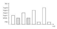
도 2는 일반적인 플래시 메모리 장치에서의 프로그램 방법을 설명하기 위한 도면이다.2 is a diagram for describing a program method in a general flash memory device.
먼저, 제 1 단계의 프로그램 펄스(Vpgm1)를 인가하여 선택된 메모리 셀들에 대한 프로그램을 수행한다. 이후, 선택된 메모리 셀들에 검증전압(PVB)을 인가하여 문턱전압(Vth)이 검증전압(PVB)보다 높은 메모리 셀들을 패스시킨다.First, the program pulse Vpgm1 of the first step is applied to program the selected memory cells. Thereafter, the verification voltage PVB is applied to the selected memory cells to pass the memory cells whose threshold voltage Vth is higher than the verification voltage PVB.
이후, 문턱전압(Vth)이 검증전압(PVB) 이하인 메모리 셀들에 대하여 프로그램 전압을 일정한 스텝으로 증가시켜 제 2 단계의 프로그램 펄스(Vpgm2)를 인가하여 프로그램을 수행한다. 이때, 검증전압(PVB)보다 문턱전압(Vth)이 높아 패스된 셀들에 대해서는 프로그램이 금지되도록 하여 오버 프로그램되는 것을 방지한다.Subsequently, the program voltage is increased in a predetermined step to the memory cells having the threshold voltage Vth equal to or less than the verification voltage PVB, and the program is performed by applying the program pulse Vpgm2 of the second step. At this time, the program is inhibited for the cells that have passed the threshold voltage Vth higher than the verification voltage PVB to prevent overprogramming.
마찬가지로, 제 2 단계의 프로그램 펄스(Vpgm2)를 인가하여 프로그램을 수행한 후에도 셀의 문턱전압(Vth)과 검증전압(PVB)을 비교, 모든 셀에 대한 프로그램이 완료될 때까지 프로그램 펄스를 점차 증가(Vpgm3, Vpgm4, …)시키면서 프로그램 및 검증을 수행한다.Similarly, even after the program is executed by applying the program pulse Vpgm2 of the second step, the threshold voltage Vth and the verify voltage PVB of the cell are compared, and the program pulse is gradually increased until the program for all cells is completed. Program and verify with (Vpgm3, Vpgm4,…).
만약, 프로그램 대상이 되는 모든 메모리 셀이 동일한 프로그램 속도를 갖는다면 프로그램이 완료된 후 프로그램된 메모리 셀의 문턱전압이 프로그램 전과 동일한 분포를 갖게 될 것이다.If all the memory cells to be programmed have the same program speed, the threshold voltages of the programmed memory cells after the program is completed will have the same distribution as before the program.
하지만 메모리 장치의 제조 공정 상에 발생되는 여러 가지 이유, 메모리 장치의 사용량에 따른 외부 조건의 변화 등에 의해 메모리 셀은 동일한 프로그램 속도를 가질 수 없다. 따라서, 프로그램 동작시 고속 프로그램되는 셀들과 저속 프로그램되는 셀들이 혼재하게 된다. 즉, 프로그램 동작은 저속 프로그램 셀들이 모두 프로그램되어야 완료될 수 있다.However, the memory cells may not have the same program speed due to various reasons occurring in the manufacturing process of the memory device, a change in external conditions according to the usage of the memory device, and the like. Therefore, cells programmed at high speed and cells programmed at low speed are mixed in the program operation. That is, the program operation can be completed when all of the low speed program cells are programmed.
이와 같이 프로그램 속도의 차이가 존재함에도 불구하고, 동일한 프로그램 펄스에 의해 동일한 시간동안 프로그램이 수행되면, 고속 프로그램 셀의 문턱전압이 계속 상승하여 저속 프로그램 셀과의 문턱전압 차이가 크게 벌어지게 된다.Even though there is a difference in program speed as described above, when the program is executed for the same time by the same program pulse, the threshold voltage of the high speed program cell continues to increase, thereby greatly increasing the threshold voltage difference with the low speed program cell.
도 3은 일반적인 플래시 메모리 장치에서 셀의 문턱전압 분포를 설명하기 위한 도면이다.3 is a diagram illustrating a threshold voltage distribution of a cell in a general flash memory device.
문턱전압 레벨이 낮은 셀들(CL0)을 높은 문턱전압 레벨의 셀들(CL1)로 프로그램하는 경우를 가정한다.Assume a case where cells CL0 having a low threshold voltage level are programmed to cells CL1 having a high threshold voltage level.
문턱전압 레벨이 낮은 셀들(CL0) 중에는 고속 프로그램 셀(FC)과 저속 프로그램 셀(SC)이 혼재되어 있으며, 이들에 대하여 동일한 프로그램 펄스를 동일한 시간동안 인가함에 따라, 이미 프로그램된 고속 프로그램 셀(FC)의 문턱전압이 계속 상승한다.Among the cells CL0 having a low threshold voltage level, the high speed program cell FC and the low speed program cell SC are mixed, and the same program pulse is applied to the high speed program cell FC as the same program pulse is applied for the same time. Threshold voltage continues to rise.
프로그램 동작은 모든 셀의 문턱전압이 검증전압(PVB)보다 커야 완료되는데, 이와 같은 과정이 진행되는 동안 고속 프로그램 셀(FC)의 문턱전압은 계속 상승하여, 문턱전압 레벨이 높은 셀들(CL1)의 문턱전압 분포가 넓어지게 하는 결과를 초래한다.The program operation is completed when the threshold voltages of all the cells are greater than the verification voltage PVB. During this process, the threshold voltages of the fast program cells FC continue to rise, so that the cells CL1 having the high threshold voltage levels are maintained. This results in widening the threshold voltage distribution.
셀의 문턱전압 분포가 넓어지는 것을 방지하기 위해서, 프로그램 펄스의 증가 정도를 작게 하여, 세밀하게 프로그램하는 방법을 고려할 수 있다. 하지만, 프로그램 펄스가 세밀하게 증가함에 따라 프로그램에 긴 시간이 소요되고, 긴 시간 동안 프로그램이 수행됨에 따라 셀간 간섭 현상에 의해 오류가 발생하는 등의 문제를 배제할 수 없다.In order to prevent the threshold voltage distribution of the cell from being widened, a method of finely programming with a small increase in the program pulse can be considered. However, as the program pulse increases in detail, the program takes a long time, and as the program is executed for a long time, an error occurs due to an inter-cell interference phenomenon.
더욱이 플래시 메모리 장치에서 셀의 문턱전압 분포는 오버 프로그램과 리드 마진에 따른 디바이스 성능을 좌우하는 요소이다. 따라서 셀의 문턱전압 분포를 고르게 하기 위한 다양한 연구가 이루어지고 있는 실정이다.In addition, the threshold voltage distribution of a cell in a flash memory device is a factor in determining device performance according to over program and read margin. Therefore, various studies have been conducted to even the threshold voltage distribution of the cell.
본 발명은 셀의 문턱전압 분포를 고르게 할 수 있는 플래시 메모리 장치 및 프로그램 검증 방법을 제공하는 데 그 기술적 과제가 있다.The present invention has a technical problem to provide a flash memory device and a program verification method that can evenly distribute the threshold voltage of a cell.
본 발명의 다른 기술적 과제는 리드 마진을 향상시킨 플래시 메모리 장치 및 프로그램 검증 방법을 제공하는 데 있다.Another object of the present invention is to provide a flash memory device and a program verification method having improved read margins.
상술한 기술적 과제를 달성하기 위한 본 발명의 일 실시예에 의한 플래시 메모리 장치는 메모리 셀 어레이; 동작 모드에 따라 동작 전압을 생성하여 상기 메모리 셀 어레이로 제공하는 전압 공급부; 및 메모리 셀의 문턱전압을 제 2 검증전압 이상으로 프로그램하는 프로그램 검증 동작시 상기 제 2 검증전압 및 상기 제 2 검증전압보다 높은 레벨의 제 1 검증전압을 상기 메모리 셀 어레이로 제공하며, 프로그램을 위해 선택된 메모리 셀에 대하여 문턱전압이 상기 제 1 검증전압보다 높은 셀이 적어도 하나 검출되면, 상기 선택된 메모리 셀 중 문턱전압이 상기 제 2 검증전압보다 높은 메모리 셀을 검출하여 프로그램 금지 상태로 설정하는 컨트롤러;를 포함할 수 있다.According to an aspect of the present invention, there is provided a flash memory device including a memory cell array; A voltage supply unit configured to generate an operating voltage according to an operation mode and provide the operating voltage to the memory cell array; And providing a first verify voltage having a level higher than the second verify voltage and the second verify voltage to the memory cell array during a program verify operation of programming a threshold voltage of a memory cell above a second verify voltage. A controller configured to detect a memory cell having a threshold voltage higher than the second verification voltage and set the program prohibition state when at least one cell having a threshold voltage higher than the first verification voltage is detected for the selected memory cell; It may include.
한편, 본 발명의 일 실시예에 의한 프로그램 검증 방법은 컨트롤러의 제어에 의해 메모리 셀 어레이의 선택된 메모리 셀을 제 2 검증전압 이상으로 프로그램하는 플래시 메모리 장치의 프로그램 검증 방법으로서, 프로그램 펄스를 인가하여 상기 선택된 메모리 셀이 프로그램됨에 따라, 상기 제 2 검증전압 보다 높은 레벨의 제 1 검증전압을 제공받아, 상기 제 1 검증전압보다 문턱전압이 높은 셀이 적어도 하나 검출되면, 상기 선택된 메모리 셀 중 문턱전압이 상기 제 2 검증전압보다 높은 메모리 셀을 고속 프로그램 셀로 검출하는 단계; 및 상기 선택된 메모리 셀 중 고속 프로그램 셀로 검출된 셀을 제외한 메모리 셀에 대하여 상기 프로그램 펄스를 순차적으로 증가시켜 프로그램이 수행됨에 따라, 상기 제 2 검증전압에 의해 프로그램 검증을 수행하는 단계;를 포함할 수 있다.Meanwhile, the program verifying method according to an exemplary embodiment of the present invention is a program verifying method of a flash memory device for programming a selected memory cell of a memory cell array above a second verifying voltage under the control of a controller. When the selected memory cell is programmed, when a first verification voltage having a level higher than the second verification voltage is received and at least one cell having a threshold voltage higher than the first verification voltage is detected, a threshold voltage among the selected memory cells is increased. Detecting a memory cell higher than the second verify voltage as a fast program cell; And performing a program verification by the second verification voltage as the program is sequentially performed on the memory cells except for the cells detected as the fast program cells among the selected memory cells. have.
본 발명에서는 프로그램 동작시 프로그램이 완료된 고속 프로그램 셀들을 먼저 검출하여 프로그램이 금지되도록 한 상태에서, 프로그램 펄스를 증가시켜 나머지 셀들에 대한 프로그램을 수행한다.According to the present invention, a program pulse is increased to detect a fast program cell in which a program is completed and the program is inhibited.
따라서, 고속 프로그램 셀들에 불필요한 프로그램 펄스가 인가되는 것을 방지하여 문턱전압이 상승하는 것을 방지할 수 있다.Therefore, it is possible to prevent unnecessary program pulses from being applied to the high-speed program cells, thereby preventing the threshold voltage from rising.
셀의 문턱전압 분포는 메모리 셀의 리드 마진을 결정하는 중요한 요소이다. 본 발명에서는 고속 프로그램 셀들을 먼저 검출하여 두고, 이후 저속 프로그램 셀들에 대한 프로그램을 완료함으로써, 셀의 문턱전압 분포를 고르게 할 수 있다.The threshold voltage distribution of the cell is an important factor in determining the read margin of the memory cell. According to the present invention, the threshold voltage distribution of the cell can be evened by detecting the high speed program cells first and then completing the program for the low speed program cells.
결국, 플래시 메모리 장치의 리드 마진을 개선함은 물론, 셀 데이터의 분포 마진 확대, 데이터 리텐션(retention) 특성 또한 향상시킬 수 있다.As a result, the read margin of the flash memory device may be improved, as well as the distribution margin of the cell data may be expanded and the data retention characteristic may be improved.
도 1은 일반적인 플래시 메모리 장치의 구성도,
도 2는 일반적인 플래시 메모리 장치에서의 프로그램 방법을 설명하기 위한 도면,
도 3은 일반적인 플래시 메모리 장치에서 셀의 문턱전압 분포를 설명하기 위한 도면,
도 4는 본 발명의 일 실시예에 의한 플래시 메모리 장치의 구성도,
도 5는 본 발명의 일 실시예에 의한 플래시 메모리 장치의 프로그램 검증 방법을 설명하기 위한 흐름도,
도 6은 도 5에 도시한 고속 프로그램 셀 검출 과정을 설명하기 위한 흐름도,
도 7은 본 발명의 일 실시예에 의한 프로그램 검증 방법을 설명하기 위한 개념도,
도 8은 본 발명에 의한 프로그램 검증 방법에 따른 셀의 문턱전압 분포를 설명하기 위한 도면이다.1 is a configuration diagram of a general flash memory device;
2 is a diagram for describing a program method in a general flash memory device;
3 is a diagram illustrating a threshold voltage distribution of a cell in a general flash memory device;
4 is a configuration diagram of a flash memory device according to an embodiment of the present invention;
5 is a flowchart illustrating a program verification method of a flash memory device according to an embodiment of the present invention;
6 is a flowchart for explaining a fast program cell detection process shown in FIG. 5;
7 is a conceptual diagram illustrating a program verification method according to an embodiment of the present invention;
8 is a diagram illustrating a threshold voltage distribution of a cell according to the program verifying method according to the present invention.
이하, 첨부된 도면을 참조하여 본 발명의 실시예를 보다 구체적으로 설명한다.Hereinafter, with reference to the accompanying drawings will be described an embodiment of the present invention in more detail.
도 4는 본 발명의 일 실시예에 의한 플래시 메모리 장치의 구성도이다.4 is a block diagram of a flash memory device according to an embodiment of the present invention.
도 4를 참조하면, 본 발명의 일 실시예에 의한 플래시 메모리 장치(20)는 전체적인 동작을 제어하는 컨트롤러(270), 메모리 셀 어레이(210), 페이지 버퍼부(220), Y 디코더(230), X 디코더(240), 전압 공급부(250) 및 검증전압 제어부(260)를 포함한다.Referring to FIG. 4, a
메모리 셀 어레이(210)에는 데이터를 저장하는 복수의 메모리 셀이 메모리 셀을 선택하여 활성화하는 워드라인(WL)과 메모리 셀의 데이터를 입출력하는 비트라인(BL) 간에 매트릭스 형태로 접속되어 있다.In the
페이지 버퍼부(220)는 비트라인(BL)을 통해 메모리 셀 어레이(210)와 접속되는 복수의 페이지 버퍼를 포함하여, 메모리 셀 어레이(210)의 선택된 메모리 셀에 프로그램 데이터를 제공하거나, 메모리 셀 어레이(210)의 선택된 메모리 셀로부터 데이터를 리드하여 저장한다.The
Y 디코더(230)는 컨트롤러(260)의 제어에 따라 페이지 버퍼부(220)의 페이지 버퍼들에 데이터 입출력 경로를 제공하며, X 디코더(240)는 컨트롤러(260)의 제어에 따라 메모리 셀 어레이(210)의 워드라인(WL)을 선택한다.The
전압 공급부(250)는 컨트롤러(260)의 제어에 따라 동작 모드(프로그램, 소거, 리드)에 따른 동작 전압을 생성하고, 생성된 동작 전압을 X 디코더(240)를 통해 워드라인(WL) 또는 페이지 버퍼부(220)로 공급한다.The
검증전압 제어부(260)는 선택된 메모리 셀의 문턱전압을 제 1 레벨 이상으로 프로그램하는 프로그램 검증 동작시 고속 프로그램 셀을 검출하기 위한 제 1 검증전압 및 저속 메모리 셀을 검출하기 위한 제 2 검증전압을 전압 공급부(250)로 제공한다. 본 실시예에서는 검증전압 제어부(260)가 컨트롤러(270)와 별도의 구성을 갖는 것으로 도시하였으나 이에 한정되지 않는다. 즉, 검증전압 제어부(260)는 컨트롤러(270) 내에 포함시켜, 컨트롤러(270)가 검증전압 제어부(260)의 기능을 수행하도록 구성하는 것도 가능하다.The verify
여기에서, 프로그램은 ISPP 방식으로 수행될 수 있으며, 제 1 검증전압은 제 1 레벨보다 크고 최초 프로그램 펄스의 레벨보다 작은 레벨을 갖도록 설정할 수 있다. 그리고, 제 2 검증전압은 제 1 레벨의 전압이 될 수 있다.Here, the program may be performed in an ISPP manner, and the first verify voltage may be set to have a level larger than the first level and smaller than the level of the initial program pulse. The second verification voltage may be a voltage of a first level.
보다 구체적으로 설명하면, 선택된 메모리 셀에 대해 ISPP 방식으로 프로그램 동작을 수행할 때, 최초 프로그램 펄스를 인가하여 프로그램을 수행한다. 이후, 검증 과정이 수행되는데, 검증전압 제어부(260)는 제 1 레벨보다 크고 최초 프로그램 펄스의 레벨보다 작은 레벨의 제 1 검증전압을 전압 공급부(250)로 제공한다. 이에 따라, 컨트롤러(270)는 프로그램 대상 메모리 셀들 중 문턱전압이 제 1 검증전압보다 높은 셀이 하나라도 검출되는지 확인한다.In more detail, when the program operation is performed in the ISPP method on the selected memory cell, the program is performed by applying an initial program pulse. Thereafter, a verification process is performed, and the
문턱전압이 제 1 검증전압보다 높은 적어도 하나의 셀이 검출되는 경우, 컨트롤러(270)는 해당 셀들을 프로그램 완료된 셀들로 판단하여 프로그램 금지 상태로 설정한다. 아울러, 컨트롤러(270)는 문턱전압이 제 1 레벨보다 크고 제 1 검증전압보다 낮은 메모리 셀들을 검출, 마찬가지로 프로그램 완료된 셀들로 판단하여 프로그램 금지 상태로 설정한다.When at least one cell having a threshold voltage higher than the first verification voltage is detected, the
이러한 상태에서 모든 메모리 셀에 대한 프로그램이 완료되지 않은 경우에는 프로그램 펄스를 일정 스텝으로 증가시켜, 프로그램 미완료된 셀들에 대해 프로그램 펄스를 인가한다. 아울러, 검증전압 제어부(260)는 전압 공급부(250)로 제 1 레벨의 전압을 제 2 검증전압으로 제공한다. 컨트롤러(270)는 제 2 검증전압을 이용한 검증을 수행, 모든 셀에 대한 프로그램이 완료될 때까지 프로그램 펄스를 증가시키면서 제 1 레벨의 제 2 검증전압을 이용한 프로그램 검증을 수행한다.In this state, when the program for all the memory cells is not completed, the program pulse is incremented by a predetermined step to apply a program pulse to the cells which are not programmed. In addition, the
결국, 제 1 검증전압에 의해 고속 프로그램 셀들을 검출하여 프로그램 금지 상태로 설정한 후, 프로그램이 미완료된 저속 프로그램 셀들에 대해 프로그램 펄스를 인가하여, 이미 프로그램이 완료된 셀들에 불필요한 프로그램 펄스가 인가되어 문턱전압이 상승하는 것을 방지할 수 있다.As a result, after detecting the high-speed program cells by the first verification voltage and setting the program-prohibited state, a program pulse is applied to the low-speed program cells in which the program is not completed, and unnecessary program pulses are applied to the cells in which the program is completed. It is possible to prevent the voltage from rising.
도 5는 본 발명의 일 실시예에 의한 플래시 메모리 장치의 프로그램 검증 방법을 설명하기 위한 흐름도이다.5 is a flowchart illustrating a program verification method of a flash memory device according to an exemplary embodiment of the present invention.
플래시 메모리 장치에서, 선택된 메모리 셀들의 문턱전압이 제 1 레벨(PVB)이상이 되도록 프로그램하기 위하여 페이지 버퍼부(220)로 데이터를 입력하여(S10) ISPP(Incremental Step Pulse Program) 방식으로 프로그램을 수행(S20)한 후에는 전압 공급부(250), 검증전압 제어부(260) 및 제어부(270)에 의해 모든 셀의 문턱전압이 기 설정된 레벨을 초과하는지 확인하는 검증 과정이 수행된다.In the flash memory device, in order to program the threshold voltages of the selected memory cells to be equal to or greater than the first level PVB, data is input to the page buffer unit 220 (S10) to perform a program in an incremental step pulse program (ISPP) method. After operation S20, a verification process is performed by the
본 발명에서는 고속 프로그램 셀들에 대해 불필요한 프로그램 펄스가 인가되는 것을 방지하기 위해, 최초 프로그램 펄스를 이용하여 프로그램을 수행한 후(S20), 제 1 검증 전압을 이용하여 고속 프로그램 셀을 검출한다(S30).In the present invention, in order to prevent unnecessary program pulses from being applied to the fast program cells, after the program is executed using the first program pulse (S20), the fast program cell is detected using the first verify voltage (S30). .
고속 프로그램 셀을 검출하는 방법은 도 6에 도시하였다.A method of detecting a fast program cell is shown in FIG.
도 6을 참조하면, 컨트롤러(270)는 최초 프로그램 펄스에 의해 프로그램이 수행된 셀들 중, 문턱전압이 제 1 검증전압(MPVB)을 초과하는 셀이 적어도 하나라도 검출되는지 확인한다(S301). 여기에서, 제 1 검증전압(MPVB)의 레벨은 제 1 레벨보다 크고 최초 프로그램 펄스의 레벨보다 작은 레벨을 갖도록 설정한다. 아울러, 제 2 검증전압(PVB)은 제 1 레벨의 전압이 될 수 있다.Referring to FIG. 6, the
만약, 단계 S301의 확인 결과 문턱전압이 제 1 검증전압(MPVB)보다 높은 셀이 검출되지 않으면, 컨트롤러(270)는 프로그램 펄스를 증가시켜 다시 프로그램을 수행한다. 반면, 문턱전압이 제 1 검증전압(MPVB)보다 높은 셀이 하나라도 검출되면 컨트롤러(270)는 문턱전압이 제 2 검증전압(PVB)보다 높은 셀들을 프로그램 금지 상태로 설정한다(S303).If the cell of which the threshold voltage is higher than the first verification voltage MPVB is not detected as a result of checking in step S301, the
결국, 단계 S301 및 S303을 통해 프로그램 속도가 빠른 셀들을 검출하여 프로그램 금지 상태로 설정할 수 있게 된다.As a result, cells having a high program speed can be detected and set to a program inhibit state through steps S301 and S303.
이후, 컨트롤러(270)는 선택된 모든 셀이 프로그램되었는지 즉, 선택된 모든 셀의 문턱전압이 제 2 검증전압(PVB)보다 큰지 확인한다(S40). 만약, 선택된 모든 셀의 문턱전압이 제 2 검증전압(PVB) 즉, 제 1 레벨보다 크면 프로그램 동작을 완료한다(S70).Thereafter, the
한편, 선택된 셀 중 문턱전압이 제 2 검증전압(PVB) 이하인 셀이 존재하는 경우에는 프로그램 펄스를 증가시켜 프로그램을 수행하고(S50), 제 2 검증전압(PVB)을 이용한 검증 과정을 수행한다(S60).On the other hand, if there is a cell having a threshold voltage less than or equal to the second verification voltage PVB among the selected cells, the program is increased by increasing the program pulse (S50), and a verification process using the second verification voltage PVB is performed ( S60).
고속 프로그램 셀 검출 후의 프로그램 및 검증 과정(S50, S60)은 선택된 모든 셀에 대한 프로그램이 완료될 때까지 반복 수행됨은 물론이다.The program and verification process (S50, S60) after the fast program cell detection is repeatedly performed until the program for all selected cells is completed.
도 7은 본 발명의 일 실시예에 의한 프로그램 검증 방법을 설명하기 위한 개념도이다.7 is a conceptual diagram illustrating a program verification method according to an embodiment of the present invention.
본 발명에서는 ISPP 방식의 프로그램 과정 중, 프로그램 검증을 수행하기 위해 셀의 목표 문턱전압(제 1 레벨, 제 2 검증전압)보다 높고, 최초 프로그램 펄스의 레벨(Vpgm1)보다 낮은 레벨의 제 1 검증전압(MPVB)을 이용하여 검증을 수행한다. 즉, 고속 프로그램 셀을 검출하는 것이다.In the present invention, during the ISPP program process, a first verification voltage higher than a target threshold voltage (first level and second verification voltage) of a cell and lower than a level Vpgm1 of an initial program pulse to perform program verification. Perform verification using (MPVB). In other words, the fast program cell is detected.
문턱전압이 제 1 검증전압(MPVB)보다 큰 적어도 하나의 셀이 검출되면, 문턱전압이 제 2 검증전압(PVB)보다 큰 메모리 셀을 프로그램 금지 상태로 설정하여, 더 이상 프로그램 펄스가 인가되지 않도록 한다.When at least one cell having a threshold voltage greater than the first verification voltage MPVB is detected, the memory cell having the threshold voltage greater than the second verification voltage PVB is set to the program inhibited state so that a program pulse is no longer applied. do.
이후에는 프로그램 미완료된 셀에 대해 프로그램 펄스를 증가시키면서 제 2 검증전압(PVB)을 이용한 검증을 수행, 모든 셀이 프로그램되도록 한다.Subsequently, verification is performed using the second verification voltage PVB while increasing the program pulse with respect to the unprogrammed cells so that all cells are programmed.
도 8은 본 발명에 의한 프로그램 검증 방법에 따른 셀의 문턱전압 분포를 설명하기 위한 도면이다.8 is a diagram illustrating a threshold voltage distribution of a cell according to the program verifying method according to the present invention.
고속 프로그램 셀들을 미리 검출하여 프로그램 금지 상태로 설정함에 따라, 도 8에 도시한 것과 같이 셀의 문턱전압 분포를 고르게 할 수 있다.By detecting the high-speed program cells in advance and setting them to the program prohibition state, the threshold voltage distribution of the cells can be evened as shown in FIG. 8.
즉, 프로그램 속도가 빨라 이미 프로그램이 완료되었는데도 동일한 프로그램 펄스를 동일한 시간동안 인가하였던 현재의 기술과 비교하여, 프로그램이 고속으로 완료된 셀들을 미리 분류하여 프로그램 금지 상태로 둠으로써 이들의 문턱전압이 상승하는 것을 방지할 수 있다.That is, compared with the current technology in which the same program pulse is applied for the same time even though the program is completed because the program speed is fast, the threshold voltage is increased by pre-classifying the cells in which the program is completed at high speed and leaving the program prohibit state. Can be prevented.
따라서, 플래시 메모리 장치의 리드 마진을 개선함은 물론, 셀 데이터의 분포 마진 확대, 데이터 리텐션(retention) 특성 또한 향상시킬 수 있다.Accordingly, the read margin of the flash memory device may be improved, as well as the distribution margin distribution and data retention characteristics of the cell data may be improved.
이상에서는 플래시 메모리 장치에서 프로그램 과정 중의 검증을 예로 들어 설명하였으나 본 발명은 이에 한정되지 않는다. 즉, 캐쉬 프로그램 검증, 카피백 프로그램 검증, 시스템 온 칩(SOC) 프로그램 검증 과정 등 다양한 검증 과정이 본 발명을 적용할 수 있다.In the above description, the verification during the program process in the flash memory device has been described as an example, but the present invention is not limited thereto. That is, various verification processes, such as cache program verification, copyback program verification, and system on chip (SOC) program verification, may be applied to the present invention.
이와 같이, 본 발명이 속하는 기술분야의 당업자는 본 발명이 그 기술적 사상이나 필수적 특징을 변경하지 않고서 다른 구체적인 형태로 실시될 수 있다는 것을 이해할 수 있을 것이다. 그러므로 이상에서 기술한 실시예들은 모든 면에서 예시적인 것이며 한정적인 것이 아닌 것으로서 이해해야만 한다. 본 발명의 범위는 상기 상세한 설명보다는 후술하는 특허청구범위에 의하여 나타내어지며, 특허청구범위의 의미 및 범위 그리고 그 등가개념으로부터 도출되는 모든 변경 또는 변형된 형태가 본 발명의 범위에 포함되는 것으로 해석되어야 한다.Thus, those skilled in the art will appreciate that the present invention may be embodied in other specific forms without departing from the spirit or essential characteristics thereof. It is therefore to be understood that the embodiments described above are to be considered in all respects only as illustrative and not restrictive. The scope of the present invention is defined by the appended claims rather than the detailed description and all changes or modifications derived from the meaning and scope of the claims and their equivalents are to be construed as being included within the scope of the present invention do.
20 : 플래시 메모리 장치
210 : 메모리 셀 어레이
220 : 페이지 버퍼부
230 : Y 디코더
240 : X 디코더
250 : 전압 공급부
260 : 검증전압 제어부
270 : 컨트롤러20: flash memory device
210: memory cell array
220: page buffer unit
230: Y decoder
240: X decoder
250: voltage supply
260: verification voltage control unit
270 controller
Claims (9)
Translated fromKorean동작 모드에 따라 동작 전압을 생성하여 상기 메모리 셀 어레이로 제공하는 전압 공급부; 및
메모리 셀의 문턱전압을 제 2 검증전압 이상으로 프로그램하는 프로그램 검증 동작시 상기 제 2 검증전압 및 상기 제 2 검증전압보다 높은 레벨의 제 1 검증전압을 상기 메모리 셀 어레이로 제공하며, 프로그램을 위해 선택된 메모리 셀에 대하여 문턱전압이 상기 제 1 검증전압보다 높은 셀이 적어도 하나 검출되면, 상기 선택된 메모리 셀 중 문턱전압이 상기 제 2 검증전압보다 높은 메모리 셀을 검출하여 프로그램 금지 상태로 설정하는 컨트롤러;
를 포함하는 플래시 메모리 장치.A memory cell array;
A voltage supply unit configured to generate an operating voltage according to an operation mode and provide the operating voltage to the memory cell array; And
In the program verifying operation of programming a threshold voltage of a memory cell above the second verifying voltage, the first verifying voltage having a level higher than the second verifying voltage and the second verifying voltage is provided to the memory cell array and selected for the program. A controller configured to detect a memory cell having a threshold voltage higher than the second verification voltage and set the program prohibition state when at least one cell having a threshold voltage higher than the first verification voltage is detected for the memory cell;
Flash memory device comprising a.
상기 컨트롤러는 프로그램 펄스를 순차적으로 증가시켜 상기 선택된 메모리 셀을 프로그램하며,
상기 선택된 메모리 셀의 문턱전압을 상기 제 2 검증전압 이상으로 프로그램하는 경우 상기 제 1 검증전압은 상기 제 2 검증전압보다 높고 최초 프로그램 펄스의 레벨보다 작은 레벨을 갖는 플래시 메모리 장치.The method of claim 1,
The controller sequentially increments a program pulse to program the selected memory cell,
And when the threshold voltage of the selected memory cell is programmed to be greater than or equal to the second verify voltage, the first verify voltage has a level higher than the second verify voltage and smaller than a level of an initial program pulse.
상기 컨트롤러는 상기 선택된 메모리 셀 중 프로그램 금지 상태에 있지 않은 모든 메모리 셀의 문턱전압이 상기 제 2 검증전압을 초과할 때까지 프로그램 펄스를 순차적으로 증가시켜 프로그램을 수행하는 플래시 메모리 장치.The method of claim 1,
The controller performs a program by sequentially increasing a program pulse until the threshold voltages of all the memory cells that are not in the program prohibition state among the selected memory cells exceed the second verification voltage.
프로그램 펄스를 인가하여 상기 선택된 메모리 셀이 프로그램됨에 따라, 상기 제 2 검증전압 보다 높은 레벨의 제 1 검증전압을 제공받아, 상기 제 1 검증전압보다 문턱전압이 높은 셀이 적어도 하나 검출되면, 상기 선택된 메모리 셀 중 문턱전압이 상기 제 2 검증전압보다 높은 메모리 셀을 고속 프로그램 셀로 검출하는 단계; 및
상기 선택된 메모리 셀 중 고속 프로그램 셀로 검출된 셀을 제외한 메모리 셀에 대하여 상기 프로그램 펄스를 순차적으로 증가시켜 프로그램이 수행됨에 따라, 상기 제 2 검증전압에 의해 프로그램 검증을 수행하는 단계;
를 포함하는 플래시 메모리 장치의 프로그램 검증 방법.A program verification method of a flash memory device for programming a selected memory cell of a memory cell array above a second verification voltage under control of a controller,
When the selected memory cell is programmed by applying a program pulse, when the first verification voltage of a level higher than the second verification voltage is received and at least one cell having a threshold voltage higher than the first verification voltage is detected, the selected memory cell is selected. Detecting a memory cell having a threshold voltage higher than the second verification voltage as a fast program cell among the memory cells; And
Performing program verification by the second verification voltage as the program is sequentially performed on the memory cells except for the cells detected as the high-speed program cells among the selected memory cells by sequentially increasing the program pulses;
Program verification method of a flash memory device comprising a.
상기 프로그램 펄스에 의해 프로그램된 셀 중 문턱전압이 상기 제 1 검증전압보다 높은 메모리 셀이 검출되지 않는 경우, 상기 프로그램 펄스를 증가시키도록 하는 플래시 메모리 장치의 프로그램 검증 방법.The method according to claim 6,
And if the memory cell having a threshold voltage higher than the first verification voltage is not detected among the cells programmed by the program pulse, increasing the program pulse.
상기 제 2 검증전압에 의해 프로그램 검증을 수행하는 단계는, 상기 프로그램 펄스의 레벨을 증가시켜 프로그램이 수행될 때마다 프로그램 대상 메모리 셀 중 문턱전압이 상기 제 2 검증전압보다 높은 메모리 셀을 프로그램 금지 상태로 설정하는 단계인 플래시 메모리 장치의 프로그램 검증 방법.The method according to claim 6,
In the performing of the program verify by the second verify voltage, the program prohibit state is performed by increasing the level of the program pulse so that a memory cell having a threshold voltage higher than the second verify voltage is programmed among memory cells to be programmed every time the program is executed. Program verification method of setting a memory device.
Priority Applications (2)
| Application Number | Priority Date | Filing Date | Title |
|---|---|---|---|
| KR1020100095067AKR101212745B1 (en) | 2010-09-30 | 2010-09-30 | Flash Memory Apparatus and Program Verify Method Therefor |
| US13/243,945US9007840B2 (en) | 2010-09-30 | 2011-09-23 | Semiconductor memory apparatus and program verification method |
Applications Claiming Priority (1)
| Application Number | Priority Date | Filing Date | Title |
|---|---|---|---|
| KR1020100095067AKR101212745B1 (en) | 2010-09-30 | 2010-09-30 | Flash Memory Apparatus and Program Verify Method Therefor |
Publications (2)
| Publication Number | Publication Date |
|---|---|
| KR20120033511A KR20120033511A (en) | 2012-04-09 |
| KR101212745B1true KR101212745B1 (en) | 2012-12-14 |
Family
ID=45889722
Family Applications (1)
| Application Number | Title | Priority Date | Filing Date |
|---|---|---|---|
| KR1020100095067AActiveKR101212745B1 (en) | 2010-09-30 | 2010-09-30 | Flash Memory Apparatus and Program Verify Method Therefor |
Country Status (2)
| Country | Link |
|---|---|
| US (1) | US9007840B2 (en) |
| KR (1) | KR101212745B1 (en) |
Families Citing this family (4)
| Publication number | Priority date | Publication date | Assignee | Title |
|---|---|---|---|---|
| KR102118979B1 (en)* | 2013-09-13 | 2020-06-05 | 삼성전자주식회사 | Non-volatile memory device and program method thereof |
| US10354724B2 (en)* | 2017-09-15 | 2019-07-16 | Sandisk Technologies Llc | Methods and apparatus for programming barrier modulated memory cells |
| KR102504295B1 (en) | 2017-11-24 | 2023-02-27 | 삼성전자 주식회사 | Nonvolatile Memory Device, and Programming Method Thereof |
| CN111727477A (en) | 2020-05-06 | 2020-09-29 | 长江存储科技有限责任公司 | Control method and controller of 3D NAND flash memory |
Family Cites Families (5)
| Publication number | Priority date | Publication date | Assignee | Title |
|---|---|---|---|---|
| US7656710B1 (en)* | 2005-07-14 | 2010-02-02 | Sau Ching Wong | Adaptive operations for nonvolatile memories |
| US7352629B2 (en) | 2005-12-29 | 2008-04-01 | Sandisk Corporation | Systems for continued verification in non-volatile memory write operations |
| US7596028B2 (en)* | 2006-12-28 | 2009-09-29 | Macronix International Co., Ltd. | Variable program and program verification methods for a virtual ground memory in easing buried drain contacts |
| WO2009006513A1 (en) | 2007-07-03 | 2009-01-08 | Sandisk Corporation | Coarse/fine program verification in non-volatile memory using different reference levels for improved sensing |
| JP4693859B2 (en)* | 2008-03-21 | 2011-06-01 | 株式会社東芝 | Nonvolatile semiconductor memory device and control method thereof |
- 2010
- 2010-09-30KRKR1020100095067Apatent/KR101212745B1/enactiveActive
- 2011
- 2011-09-23USUS13/243,945patent/US9007840B2/enactiveActive
Also Published As
| Publication number | Publication date |
|---|---|
| US9007840B2 (en) | 2015-04-14 |
| US20120081970A1 (en) | 2012-04-05 |
| KR20120033511A (en) | 2012-04-09 |
Similar Documents
| Publication | Publication Date | Title |
|---|---|---|
| US10360987B2 (en) | Managing refresh for flash memory | |
| US9324436B2 (en) | Method and apparatus for controlling operation of flash memory | |
| JP6154986B2 (en) | Nonvolatile memory device and operation method thereof | |
| US8929149B2 (en) | Semiconductor memory device and method of operating the same | |
| KR102031742B1 (en) | Nonvolatile memory device and operating method thereof | |
| KR102192910B1 (en) | Semiconductor device and memory system and operating method thereof | |
| US9496041B2 (en) | Memory programming method, memory control circuit unit and memory storage device | |
| TW201346908A (en) | Enhanced programming and erasure schemes for analog memory cells | |
| TWI859181B (en) | Memory controller, memory system and operating method thereof | |
| KR20080027419A (en) | Memory system and its program method | |
| KR20120070012A (en) | Non-volatile memory device and cache program method of the same | |
| KR20140024723A (en) | Semiconductor memory device and operating method thereof | |
| KR101212745B1 (en) | Flash Memory Apparatus and Program Verify Method Therefor | |
| US8243519B2 (en) | Writing method of a nonvolatile memory device | |
| US9378829B2 (en) | Non-volatile memory device with an EPLI comparator | |
| KR20150104858A (en) | Semiconductor device and operating method thereof | |
| TWI523011B (en) | Programming and erasure schemes for analog memory cells | |
| CN104599705A (en) | Memory devices | |
| US20120159280A1 (en) | Method for controlling nonvolatile memory apparatus | |
| US8000154B2 (en) | Non-volatile memory device and method of controlling a bulk voltage thereof | |
| CN106297882A (en) | Method and apparatus for programming non-volatile memory device to reduce bit line disturb | |
| KR20140019538A (en) | Nonvolatile memory device and operating method thereof | |
| JP2006190488A (en) | Write-in method in semiconductor memory device | |
| CN112614532A (en) | SSD with parallelized multi-level program voltage verification | |
| US12327596B2 (en) | Semiconductor storage device |
Legal Events
| Date | Code | Title | Description |
|---|---|---|---|
| A201 | Request for examination | ||
| PA0109 | Patent application | Patent event code:PA01091R01D Comment text:Patent Application Patent event date:20100930 | |
| PA0201 | Request for examination | ||
| E902 | Notification of reason for refusal | ||
| PE0902 | Notice of grounds for rejection | Comment text:Notification of reason for refusal Patent event date:20111124 Patent event code:PE09021S01D | |
| PG1501 | Laying open of application | ||
| E90F | Notification of reason for final refusal | ||
| PE0902 | Notice of grounds for rejection | Comment text:Final Notice of Reason for Refusal Patent event date:20120516 Patent event code:PE09021S02D | |
| E701 | Decision to grant or registration of patent right | ||
| PE0701 | Decision of registration | Patent event code:PE07011S01D Comment text:Decision to Grant Registration Patent event date:20121127 | |
| GRNT | Written decision to grant | ||
| PR0701 | Registration of establishment | Comment text:Registration of Establishment Patent event date:20121210 Patent event code:PR07011E01D | |
| PR1002 | Payment of registration fee | Payment date:20121211 End annual number:3 Start annual number:1 | |
| PG1601 | Publication of registration | ||
| FPAY | Annual fee payment | Payment date:20151120 Year of fee payment:4 | |
| PR1001 | Payment of annual fee | Payment date:20151120 Start annual number:4 End annual number:4 | |
| FPAY | Annual fee payment | Payment date:20161125 Year of fee payment:5 | |
| PR1001 | Payment of annual fee | Payment date:20161125 Start annual number:5 End annual number:5 | |
| FPAY | Annual fee payment | Payment date:20171124 Year of fee payment:6 | |
| PR1001 | Payment of annual fee | Payment date:20171124 Start annual number:6 End annual number:6 | |
| FPAY | Annual fee payment | Payment date:20181126 Year of fee payment:7 | |
| PR1001 | Payment of annual fee | Payment date:20181126 Start annual number:7 End annual number:7 | |
| FPAY | Annual fee payment | Payment date:20191125 Year of fee payment:8 | |
| PR1001 | Payment of annual fee | Payment date:20191125 Start annual number:8 End annual number:8 | |
| PR1001 | Payment of annual fee | Payment date:20201124 Start annual number:9 End annual number:9 | |
| PR1001 | Payment of annual fee | Payment date:20221124 Start annual number:11 End annual number:11 | |
| PR1001 | Payment of annual fee | Payment date:20241126 Start annual number:13 End annual number:13 |