KR101211113B1 - Clock and data recovery circuit including binary phase detector - Google Patents
Clock and data recovery circuit including binary phase detectorDownload PDFInfo
- Publication number
- KR101211113B1 KR101211113B1KR1020110082191AKR20110082191AKR101211113B1KR 101211113 B1KR101211113 B1KR 101211113B1KR 1020110082191 AKR1020110082191 AKR 1020110082191AKR 20110082191 AKR20110082191 AKR 20110082191AKR 101211113 B1KR101211113 B1KR 101211113B1
- Authority
- KR
- South Korea
- Prior art keywords
- phase
- clock
- outputting
- current
- binary phase
- Prior art date
- Legal status (The legal status is an assumption and is not a legal conclusion. Google has not performed a legal analysis and makes no representation as to the accuracy of the status listed.)
- Active
Links
- 238000011084recoveryMethods0.000titleclaimsdescription30
- 238000000034methodMethods0.000claimsdescription5
- 239000003990capacitorSubstances0.000claimsdescription4
- 238000005070samplingMethods0.000abstractdescription4
- 238000010586diagramMethods0.000description9
- 230000005540biological transmissionEffects0.000description1
- 238000004891communicationMethods0.000description1
- 238000012986modificationMethods0.000description1
- 230000004048modificationEffects0.000description1
- 230000000737periodic effectEffects0.000description1
Images


Classifications
- H—ELECTRICITY
- H04—ELECTRIC COMMUNICATION TECHNIQUE
- H04L—TRANSMISSION OF DIGITAL INFORMATION, e.g. TELEGRAPHIC COMMUNICATION
- H04L7/00—Arrangements for synchronising receiver with transmitter
- H04L7/02—Speed or phase control by the received code signals, the signals containing no special synchronisation information
- H04L7/033—Speed or phase control by the received code signals, the signals containing no special synchronisation information using the transitions of the received signal to control the phase of the synchronising-signal-generating means, e.g. using a phase-locked loop
- H04L7/0331—Speed or phase control by the received code signals, the signals containing no special synchronisation information using the transitions of the received signal to control the phase of the synchronising-signal-generating means, e.g. using a phase-locked loop with a digital phase-locked loop [PLL] processing binary samples, e.g. add/subtract logic for correction of receiver clock
- H—ELECTRICITY
- H03—ELECTRONIC CIRCUITRY
- H03D—DEMODULATION OR TRANSFERENCE OF MODULATION FROM ONE CARRIER TO ANOTHER
- H03D13/00—Circuits for comparing the phase or frequency of two mutually-independent oscillations
- H03D13/003—Circuits for comparing the phase or frequency of two mutually-independent oscillations in which both oscillations are converted by logic means into pulses which are applied to filtering or integrating means
- H—ELECTRICITY
- H03—ELECTRONIC CIRCUITRY
- H03K—PULSE TECHNIQUE
- H03K5/00—Manipulating of pulses not covered by one of the other main groups of this subclass
- H03K5/13—Arrangements having a single output and transforming input signals into pulses delivered at desired time intervals
- H03K5/135—Arrangements having a single output and transforming input signals into pulses delivered at desired time intervals by the use of time reference signals, e.g. clock signals
- H—ELECTRICITY
- H03—ELECTRONIC CIRCUITRY
- H03L—AUTOMATIC CONTROL, STARTING, SYNCHRONISATION OR STABILISATION OF GENERATORS OF ELECTRONIC OSCILLATIONS OR PULSES
- H03L7/00—Automatic control of frequency or phase; Synchronisation
- H03L7/06—Automatic control of frequency or phase; Synchronisation using a reference signal applied to a frequency- or phase-locked loop
- H03L7/08—Details of the phase-locked loop
- H03L7/085—Details of the phase-locked loop concerning mainly the frequency- or phase-detection arrangement including the filtering or amplification of its output signal
- H03L7/093—Details of the phase-locked loop concerning mainly the frequency- or phase-detection arrangement including the filtering or amplification of its output signal using special filtering or amplification characteristics in the loop
Landscapes
- Engineering & Computer Science (AREA)
- Physics & Mathematics (AREA)
- Nonlinear Science (AREA)
- Power Engineering (AREA)
- Computer Networks & Wireless Communication (AREA)
- Signal Processing (AREA)
- Stabilization Of Oscillater, Synchronisation, Frequency Synthesizers (AREA)
Abstract
Translated fromKoreanDescription
Translated fromKorean본 발명은 클럭 및 데이터 복원 회로에 관한 것으로, 보다 구체적으로는 고속 직렬통신 등에서 NRZ (non return to zero) 형태의 비주기적 수신 데이터로부터 클럭을 복원하고, 복원된 클럭 신호를 이용하여 다시 데이터를 복원하는 클럭 및 데이터 복원회로에 관한 것이다.
The present invention relates to a clock and data recovery circuit, and more particularly, to recover a clock from non-periodic received data in the form of non return to zero (NRZ) in high speed serial communication, and to restore the data again using the restored clock signal. The present invention relates to a clock and data recovery circuit.
종래의 클럭 및 데이터 복원 회로는 바이너리 위상 검출기(binary phase detector)와 선형 위상 검출기(linear phase detector) 중 어느 하나를 선택하여 설계되었다. 특히 초고속 동작을 하는 클럭 및 데이터 복원회로는 속도, 전력 소모 및 구현의 용이함으로 인하여 일반적으로 바이너리 위상 검출기가 선호되고 있다.Conventional clock and data recovery circuits are designed by selecting one of a binary phase detector and a linear phase detector. In particular, clock and data recovery circuits that operate at high speed are generally favored by binary phase detectors due to speed, power consumption, and ease of implementation.
일반적인 바이너리 위상 검출기를 포함하는 클럭 및 데이터 복원회로의 구성 및 특징을 간단히 설명하면 다음과 같다. 도 1은 종래의 바이너리 위상 검출기를 사용한 클럭 및 데이터 복원 회로를 나타내는 블록도로서, 일반적으로 바이너리 위상 검출기(binary phase detector, 100), 챠지 펌프(charge pump, 200), 루프 필터(loop filter, 300), 전압 제어 오실레이터(VCO, 400) 및 D 플립플롭(D flipflop, 600)으로 구성된다.The configuration and features of a clock and data recovery circuit including a general binary phase detector will be briefly described as follows. 1 is a block diagram illustrating a clock and data recovery circuit using a conventional binary phase detector. In general, a
바이너리 위상 검출기를 사용할 경우, 수신 데이터와 복원된 클럭의 위상 차이에 따른 챠지 펌프의 출력 전류는, 도 2에 도시한 바와 같이 비선형 특성을 갖는다. 즉, 수신 데이터가 복원된 클럭보다 위상이 빠를 경우 챠지 펌프의 전류는 +I0가 되고, 반대로 수신 데이터가 복원된 클럭보다 위상이 느릴 경우 챠지 펌프의 전류는 -I0가 된다. 이렇게 바이너리 위상 검출기는 수신 데이터와 복원된 클럭 중에서 어느 것이 위상이 더 빠른지 만을 검출하고, 그에 따른 챠지 펌프의 전류(이 경우 +I0 또는 -I0)를 출력할 뿐, 수신 데이터와 복원된 클럭의 위상 차이의 크기를 검출하지는 못하는 한계를 갖는다.When the binary phase detector is used, the output current of the charge pump according to the phase difference between the received data and the restored clock has a nonlinear characteristic as shown in FIG. That is, when the received data is out of phase with the recovered clock, the charge pump current becomes + I0. On the contrary, when the received data is out of phase with the recovered clock, the charge pump current becomes −I0 . In this way, the binary phase detector detects only the phase of the received data and the recovered clock is faster, and outputs the current of the charge pump accordingly (+ I0 or -I0 in this case). There is a limit in not detecting the magnitude of the phase difference.
이러한 바이너리 위상 검출기의 비선형 특성은 클럭 및 데이터 복원 회로가 수신 데이터의 지터를 트래킹(jitter tracking)할 때, 수신 데이터와 복원된 클럭의 위상 차이에 상관없이 항상 일정한 속도로 수신 데이터의 지터를 트래킹하기 때문에, 도 3에 도시된 바와 같이 지터 트래킹 (jitter tracking) 시 슬루잉(slewing) 문제가 발생하며, 이는 바이너리 위상 검출기를 사용하는 클럭 및 데이터 복원 회로의 지터 톨러런스(jitter tolerance) 성능이 제한되는 주된 요인이 된다.
The nonlinear nature of these binary phase detectors ensures that when the clock and data recovery circuits track jitter of the received data, they always track the jitter of the received data at a constant rate regardless of the phase difference between the received data and the recovered clock. As a result, as shown in FIG. 3, slewing problems occur during jitter tracking, which is a major limitation in jitter tolerance performance of clock and data recovery circuits using binary phase detectors. It becomes a factor.
본 발명은 바이너리 위상 검출기(binary phase detector)의 비선형 위상 검출기 이득(nonlinear phase detector gain)으로 인하여 발생하는 수신 데이터의 지터 트래킹 (jitter tracking) 시 슬루잉(slewing) 문제를 해결하는 것을 목적으로 하는 클럭 및 데이터 복원 회로에 관한 것이다.
SUMMARY OF THE INVENTION The present invention is directed to a clock aimed at solving a slewing problem in jitter tracking of received data caused by a nonlinear phase detector gain of a binary phase detector. And a data recovery circuit.
본 발명의 일 측면에 따르면, 수신 데이터와 다 위상 복원된 클럭들의 위상 차이를 비교하여 그에 따른 업/다운 신호들을 출력하는 2n+1(여기서, n은 1 이상의 자연수) 개의 바이너리 위상 검출기(binary phase detector); 상기 바이너리 위상 검출기들로부터 입력되는 업/다운 신호들에 상응하는 업/다운 전류를 생성하는, 상기 바이너리 위상 검출기들의 개수와 동수(同數)로 구성되는 챠지 펌프(charge pump); 상기 챠지 펌프들로부터 입력되는 업/다운 전류에 상응하는 아날로그 전압 조정 신호를 출력하는 루프 필터; 상기 아날로그 전압 조정 신호에 따라 변화된 주파수의 클럭을 출력하는 전압 제어 오실레이터(VCO); 상기 전압 제어 오실레이터로부터 출력되는 클럭으로부터 상호 간 미세한 위상 차이(Dq)를 갖는 다 위상 복원된 클럭들을 출력하는 다 위상 클럭 발생기; 및 수신 데이터를 상기 다 위상 복원된 클럭들 중 어느 한 클럭으로 샘플링하여 복원된 데이터를 출력하는 D 플립플롭을 포함하는 클럭 및 데이터 복원 회로가 제공된다.
According to an aspect of the present invention, 2n + 1 binary phase detectors (n, where n is a natural number of 1 or more) for comparing the phase difference between the received data and the multi-phase reconstructed clocks and outputting corresponding up / down signals. detector); A charge pump configured to equal the number of the binary phase detectors to generate an up / down current corresponding to the up / down signals inputted from the binary phase detectors; A loop filter outputting an analog voltage adjustment signal corresponding to an up / down current input from the charge pumps; A voltage controlled oscillator (VCO) for outputting a clock of a frequency changed according to the analog voltage adjustment signal; A multi-phase clock generator for outputting multi-phase reconstructed clocks having a fine phase difference Dq from each other from a clock output from the voltage controlled oscillator; And a D flip-flop for sampling received data with one of the multi-phase recovered clocks and outputting the recovered data.
본 발명의 실시예에 의하면, 종래의 클럭 및 데이터 복원회로와 달리 새로이 제안하는 홀수 개의 바이너리 위상 검출기(binary phase detector)들과 동수의 챠지 펌프들을 사용하여 구현함으로써, 수신 데이터와 복원된 클럭 간의 위상 차이가 클 경우, 보다 큰 챠지 펌프 전류를 루프 필터에 흐르게 하여 지터 트래킹(jitter tracking) 시 슬루잉(slewing) 문제를 완화하고, 클럭 및 데이터 복원 회로의 지터 톨러런스 (jitter tolerance) 성능을 향상시키는 장점을 가지고 있다.
According to an embodiment of the present invention, unlike the conventional clock and data recovery circuit, the phase between the received data and the recovered clock is implemented by using the newly proposed odd number of binary phase detectors and the same number of charge pumps. Larger differences allow larger charge pump currents to flow through the loop filter to mitigate slewing during jitter tracking and improve jitter tolerance in clock and data recovery circuits Have
도 1은 종래의 바이너리 위상 검출기(binary phase detector)를 사용한 클럭 및 데이터 복원 회로를 나타내는 블록도.
도 2는 도 1의 종래의 바이너리 위상 검출기(binary phase detector)를 사용할 경우, 수신 데이터와 복원된 클럭의 위상 차이에 따른 챠지 펌프 출력 전류를 나타낸 도면.
도 3은 바이너리 위상 검출기(binary phase detector)를 사용할 경우, 시간에 따라 복원된 클럭의 위상이 수신 데이터의 위상을 트래킹하는 파형을 나타낸 도면.
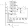
도 4는 본 발명의 일 실시예에 따른 3개의 바이너리 위상 검출기(binary phase detector)들을 사용한 클럭 및 데이터 복원 회로를 나타내는 블록도.
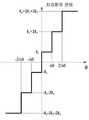
도 5는 도 4에서와 같이 3개의 바이너리 위상 검출기(binary phase detector)들을 사용할 경우, 수신 데이터와 복원된 클럭의 위상 차이에 따른 챠지 펌프 출력 전류를 나타낸 도면.
도 6은 본 발명의 다른 실시예에 따른 5개의 바이너리 위상 검출기(binary phase detector)들을 사용한 클럭 및 데이터 복원 회로를 나타내는 블록도.
도 7은 도 6에서와 같이 5개의 바이너리 위상 검출기(binary phase detector)들을 사용할 경우, 수신 데이터와 복원된 클럭의 위상 차이에 따른 챠지 펌프 출력 전류를 나타낸 도면.1 is a block diagram illustrating a clock and data recovery circuit using a conventional binary phase detector.
FIG. 2 is a diagram illustrating a charge pump output current according to a phase difference between received data and a restored clock when the conventional binary phase detector of FIG. 1 is used.
3 shows waveforms in which the phase of a clock recovered over time tracks the phase of received data when using a binary phase detector;
4 is a block diagram illustrating a clock and data recovery circuit using three binary phase detectors in accordance with one embodiment of the present invention.
FIG. 5 is a diagram illustrating a charge pump output current according to a phase difference between received data and a restored clock when using three binary phase detectors as in FIG. 4; FIG.
6 is a block diagram illustrating a clock and data recovery circuit using five binary phase detectors in accordance with another embodiment of the present invention.
FIG. 7 is a diagram illustrating a charge pump output current according to a phase difference between received data and a restored clock when five binary phase detectors are used as shown in FIG. 6.
본 발명은 다양한 변경을 가할 수 있고 여러 가지 실시예를 가질 수 있는 바, 특정 실시예들을 도면에 예시하고 이를 상세한 설명을 통해 상세히 설명하고자 한다. 그러나, 이는 본 발명을 특정한 실시 형태에 대해 한정하려는 것이 아니며, 본 발명의 사상 및 기술 범위에 포함되는 모든 변경, 균등물 내지 대체물을 포함하는 것으로 이해되어야 한다.The present invention may be variously modified and have various embodiments, and specific embodiments will be illustrated in the drawings and described in detail with reference to the accompanying drawings. It should be understood, however, that the invention is not intended to be limited to the particular embodiments, but includes all modifications, equivalents, and alternatives falling within the spirit and scope of the invention.
본 발명을 설명함에 있어서, 관련된 공지 기술에 대한 구체적인 설명이 본 발명의 요지를 불필요하게 흐릴 수 있다고 판단되는 경우 그 상세한 설명을 생략한다. 또한, 본 명세서의 설명 과정에서 이용되는 숫자(예를 들어, 제1, 제2 등)는 하나의 구성요소를 다른 구성요소와 구분하기 위한 식별기호에 불과하다.DETAILED DESCRIPTION OF THE PREFERRED EMBODIMENTS Hereinafter, the present invention will be described in detail with reference to the accompanying drawings. In addition, numerals (e.g., first, second, etc.) used in the description of the present invention are merely an identifier for distinguishing one component from another.
이하, 첨부된 도면들을 참조하여 본 발명의 실시예들에 관하여 상세히 설명한다.
Hereinafter, embodiments of the present invention will be described in detail with reference to the accompanying drawings.
도 4는 본 발명의 일 실시예에 따른 3개의 바이너리 위상 검출기(binary phase detector)를 사용한 클럭 및 데이터 복원 회로를 나타내는 블록도이다.4 is a block diagram illustrating a clock and data recovery circuit using three binary phase detectors according to an embodiment of the present invention.
도 1에 도시한 종래의 바이너리 위상 검출기(binary phase detector, 100) 와 챠지 펌프(charge pump, 200)를 사용한 클럭 및 데이터 복원 회로에 추가적으로 두 개의 바이너리 위상 검출기(110, 120), 두 개의 챠지 펌프(210, 220) 및 상호 간 미세한 위상 차이(Dq)를 갖는 다 위상 클럭들을 출력하는 다 위상 클럭 발생기(500)를 포함하여 구성된다. 도 4에 도시된 다 위상 클럭 발생기(500)는 일례로 3개의 위상을 갖는 클럭들을 출력하고 있다.In addition to the clock and data recovery circuit using the conventional
따라서, 본 발명의 일 실시예에 따른 클럭 및 데이터 복원회로는, 수신 데이터와 복원된 다 위상 클럭들의 위상 차이를 비교하여 그에 따른 업/다운 신호들을 출력하는 3개의 바이너리 위상 검출기(100, 110, 120), 상기 3개의 바이너리 위상 검출기(100, 110, 120)들로부터 입력되는 업/다운 신호들에 상응하는 업/다운 전류를 생성하는 3개의 챠지 펌프(200, 210, 220), 상기 3개의 챠지 펌프(200, 210, 220)들로부터 입력되는 업/다운 전류에 상응하는 아날로그 전압 조정 신호를 출력하는 루프 필터(300), 상기 아날로그 전압 조정 신호에 따라 주파수가 변하는 전압 제어 오실레이터(VCO, 400), 상기 전압 제어 오실레이터(400)로부터 출력되는 클럭으로부터 상호 미세한 위상 차이(Dq)를 갖는 다 위상 복원된 클럭들을 출력하는 다 위상 클럭 발생기(500), 및 수신 데이터를 상기 다 위상 복원된 클럭들 중 어느 한 클럭으로 샘플링하여 복원된 데이터를 출력하는 D 플립플롭(600)으로 구성될 수 있다.Accordingly, the clock and data recovery circuits according to an embodiment of the present invention compare three phase differences between the received data and the restored multi-phase clocks and output three up / down signals according to the three
여기서, 바이너리 위상 검출기(100, 110, 120) 각각은, 수신 데이터와 복원된 클럭의 위상 차이를 비교하여, 수신 데이터의 위상이 복원된 클럭의 위상보다 앞서면(즉, 빠르면) 업 신호를 출력하고, 뒤지면(즉, 느리면) 다운 신호를 출력한다. 이러한 업 신호 또는 다운 신호는, 각 바이너리 위상 검출기(100, 110, 120)의 출력단과 연결된 챠지 펌프(200, 210, 220)로 입력된다.Here, each of the
이 경우, 챠지 펌프(200, 210, 220)는 바이너리 위상 검출기(100, 110, 120)로부터 각각 입력된 업/다운 신호에 상응하는 업/다운 전류를 생성하게 된다. 이를 위해, 챠지 펌프(200, 210, 220) 각각에는 업 전류를 생성하는 업 전류원 및 다운 전류를 생성하는 다운 전류원이 포함될 수 있다.In this case, the
루프 필터(300)는 챠지 펌프(200, 210, 220)들로부터 입력되는 업/다운 전류에 상응하는 아날로그 전압 조정 신호를 출력한다. 구체적으로, 루프 필터(300)는, 챠지 펌프(200, 210, 220)의 출력단과 접지 사이에 서로 직렬 연결된 저항(R) 및 제1 캐패시터(C1)와, 챠지 펌프(200, 210, 220)의 출력단과 접지 사이에 연결된 제2 캐패시터(C2)를 포함하여 구성될 수 있다. 이에 따라, 챠지 펌프(200, 210, 220)들로부터 출력된 업/다운 전류는 루프 필터(300)를 거치면서 전압 제어 오실레이터(400)의 조정 전압으로 바뀌게 된다.The
전압 제어 오실레이터(400)는, 상기 루프 필터(300)에서 출력되는 아날로그 전압 조정 신호에 따라 변화된 주파수 및 위상을 갖는 클럭을 복원하고, 복원된 클럭을 다 위상 클럭 발생기(500)로 피드백시킨다.The
다 위상 클럭 발생기(500)는, 전압 제어 오실레이터(400)로부터 출력된 클럭을 입력받고, 상호 미세한 위상 차이(Dq)를 갖는 다 위상 복원된 클럭들을 출력한다. 이러한 다 위상 클럭 발생기(500)는 도 4에 도시된 바와 같이, 복수의 미세 지연셀들로 구성될 수 있다. 이때, 미세 지연셀은 바이너리 위상 검출기(100, 110, 120)의 개수와 동수로 구성될 수 있다. 그리고 미세 지연셀은 복원된 클럭의 주파수에 따라서, 구체적으로 인버터(inverter)로 구현되거나, 저이득 차동 증폭기(low gain differential amplifier)로 구현되거나, 또는 전송선(transmission line)등으로 구현될 수 있다.The
그리고 D 플리플롭(600)은, 수신 데이터 및 상기 다 위상 클럭 발생기(500)에 의해 복원된 클럭들 중 어느 한 클럭을 입력받고, 수신 데이터를 상기 다 위상 복원된 클럭들 중 입력된 어느 한 클럭으로 샘플링하여 복원 데이터를 생성(출력)한다.The D flip-
이상에서는 도 4의 클럭 및 데이터 복원 회로의 상세 구성에 대하여 설명하였는 바, 이하, 도 4의 클럭 및 데이터 복원 회로의 특징에 대하여 설명하기로 한다. 이를 위해, 도 4에서 종래의 챠지 펌프(200) 의 전류량을 I0라고 하고, 본 발명의 일 실시예에 따라 추가된 두 개의 챠지 펌프(210, 220)의 전류량을 I1이라 가정한다.The detailed configuration of the clock and data recovery circuit of FIG. 4 has been described above. Hereinafter, the features of the clock and data recovery circuit of FIG. 4 will be described. To this end, in FIG. 4, the current amount of the
제1 케이스로서, 도 4의 다 위상 클럭 발생기(500)로부터 출력된 3개의 위상을 갖는 클럭들의 위상이 모두 수신 데이터의 위상 보다 느릴 경우, 첫 번째 챠지 펌프(210) 의 전류는 I1, 두 번째 챠지 펌프(200)의 전류는 I0 그리고 세 번째 챠지 펌프(220)의 전류는 I1이 되어 총 I0+2I1의 전류가 3개의 챠지 펌프(200, 210, 220)들로부터 출력된다.As a first case, when the phases of the clocks having three phases output from the
제2 케이스로서, 도 4의 다 위상 클럭 발생기(500)로부터 출력된 3개의 위상을 갖는 클럭들 중 위상이 제일 빠른 클럭의 위상이 수신 데이터의 위상 보다 빠르고, 나머지 두 클럭들의 위상이 수신 데이터의 위상 보다 느릴 경우, 첫 번째 챠지 펌프(210)의 전류는 -I1, 두 번째 챠지 펌프(200)의 전류는 I0 그리고 세 번째 챠지 펌프(220)의 전류는 I1이 되어 총 I0의 전류가 3개의 챠지 펌프(200, 210, 220)들로부터 출력된다.As a second case, among the clocks having three phases output from the
제3 케이스로서, 도 4의 다 위상 클럭 발생기(500)로부터 출력된 3개의 위상을 갖는 클럭들 중 위상이 빠른 두 클럭의 위상이 수신 데이터의 위상 보다 빠르고, 나머지 클럭의 위상이 수신 데이터의 위상 보다 느릴 경우, 첫 번째 챠지 펌프(210)의 전류는 -I1, 두 번째 챠지 펌프(200)의 전류는 -I0 그리고 세 번째 챠지 펌프(220)의 전류는 I1이 되어 총 -I0의 전류가 3개의 챠지 펌프(200, 210, 220)들로부터 출력된다.As a third case, of the clocks having three phases output from the
마지막 제4 케이스로서, 도 4의 다 위상 클럭 발생기(500)로부터 출력된 3개의 위상을 갖는 클럭들의 위상이 모두 수신 데이터의 위상 보다 빠를 경우, 첫 번째 챠지 펌프(210)의 전류는 -I1, 두 번째 챠지 펌프(200)의 전류는 -I0 그리고 세 번째 챠지 펌프(220)의 전류는 -I1이 되어 총 -I0-2I1의 전류가 3개의 챠지 펌프(200, 210, 220)들로부터 출력된다.As a fourth case, when the phases of the three phase clocks output from the
위와 같이 3개의 챠지 펌프(200, 210, 220)들의 출력 전류는, 수신 데이터와 복원된 클럭의 위상 차이에 따라 달라지며, 이를 도시하면 도 5와 같게 된다.As described above, the output currents of the three charge pumps 200, 210, and 220 depend on the phase difference between the received data and the restored clock, which is illustrated in FIG. 5.
여기서, 도 5의 본 발명에 따른 바이너리 위상 검출기 이득 곡선과 도 3의 종래의 바이너리 위상 검출기 이득 곡선을 상호 비교하면, 본 발명의 일 실시예에 따른 바이너리 위상 검출기는, 수신 데이터와 복원된 클럭의 위상 차이(q)가 클 경우, 보다 큰 챠지 펌프 전류를 출력함으로써, 지터 트래킹시 슬루잉(slewing) 문제를 완화하고, 따라서 클럭 및 데이터 복원회로의 지터 톨러런스(jitter tolerance) 성능을 개선함을 알 수 있다.
Here, when comparing the binary phase detector gain curve of FIG. 5 with the conventional binary phase detector gain curve of FIG. If the phase difference q is large, outputting a larger charge pump current alleviates the slewing problem during jitter tracking, thus improving the jitter tolerance performance of the clock and data recovery circuitry. Can be.
아울러, 도 4에 도시된 클럭 및 데이터 복원 회로에 두 개의 바이너리 위상 검출기(130, 140)와 두 개의 챠지 펌프(230, 240)를 더 추가하고, 다 위상 클럭 발생기(500)에서 5개의 위상을 갖는 클럭들을 출력함으로써, 도 6과 같이 5개의 바이너리 위상 검출기(100, 110, 120, 130, 140)와 5개의 챠지 펌프(200, 210, 220, 230, 240)를 갖는 클럭 및 데이터 복원회로를 구현할 수도 있다. 여기서, 도 6은 본 발명의 다른 실시예에 따른 5개의 바이너리 위상 검출기(binary phase detector)들을 사용한 클럭 및 데이터 복원 회로를 나타내는 블록도이다.In addition, two
이 경우에도, 도 7에 도시한 바와 같이, 수신 데이터와 복원된 클럭의 보다 세분화된 위상 차이(q)에 따라 챠지펌프 전류의 크기가 변화됨을 알 수 있다. 보다 구체적인 설명을 위해, 도 6에서, 종래의 챠지 펌프(200) 의 전류량을 I0라고 하고, 도 4의 실시예에서와 같이 추가된 두 개의 챠지 펌프(210, 220)의 전류량을 I1이라 하고, 도 6의 실시예에서 새롭게 추가된 두 개의 차지 펌프(230, 240)의 전류량을 I2라 가정하여, 본 발명의 다른 실시예에 따른 클럭 및 데이터 복원회로의 특징을 설명하면 다음과 같다. 이는 앞선 도 4 및 도 5의 설명에서와 유사하게 설명될 수 있다.In this case also, as shown in FIG. 7, it can be seen that the magnitude of the charge pump current changes according to the more detailed phase difference q between the received data and the restored clock. For more detailed description, in FIG. 6, the current amount of the
제1 케이스로서, 도 6의 다 위상 클럭 발생기(500)로부터 출력된 5개의 위상을 갖는 클럭들의 위상이 모두 수신 데이터의 위상 보다 느릴 경우, 첫 번째 챠지 펌프(230) 의 전류는 I2, 두 번째 챠지 펌프(210)의 전류는 I1, 세 번째 챠지 펌프(200)의 전류는 I0, 네 번째 챠지 펌프(220)의 전류는 I1, 그리고 다섯 번째 챠지 펌프(240)의 전류는 I2가 되어 총 I0+2I1+2I2 의 전류가 5개의 챠지 펌프(200, 210, 220, 230, 240)들로부터 출력된다.As a first case, when the phases of the clocks having five phases output from the
제2 케이스로서, 도 6의 다 위상 클럭 발생기(500)로부터 출력된 5개의 위상을 갖는 클럭들의 위상 중 제일 빠른 클럭의 위상이 수신 데이터의 위상 보다 빠르고, 나머지 4개의 클럭들의 위상이 수신 데이터의 위상 보다 느릴 경우, 첫 번째 챠지 펌프(230) 의 전류는 -I2, 두 번째 챠지 펌프(210)의 전류는 I1, 세 번째 챠지 펌프(200)의 전류는 I0, 네 번째 챠지 펌프(220)의 전류는 I1, 그리고 다섯 번째 챠지 펌프(240)의 전류는 I2가 되어 총 I0+2I1의 전류가 5개의 챠지 펌프(200, 210, 220, 230, 240)들로부터 출력된다.As a second case, the phase of the fastest clock among the phases of the five phases output from the
제3 케이스로서, 도 6의 다 위상 클럭 발생기(500)로부터 출력된 5개의 위상을 갖는 클럭들의 위상 중 빠른 순의 2개의 클럭의 위상이 수신 데이터의 위상 보다 빠르고, 나머지 3개의 클럭들의 위상이 수신 데이터의 위상 보다 느릴 경우, 첫 번째 챠지 펌프(230) 의 전류는 -I2, 두 번째 챠지 펌프(210)의 전류는 -I1, 세 번째 챠지 펌프(200)의 전류는 I0, 네 번째 챠지 펌프(220)의 전류는 I1, 그리고 다섯 번째 챠지 펌프(240)의 전류는 I2가 되어 총 I0의 전류가 5개의 챠지 펌프(200, 210, 220, 230, 240)들로부터 출력된다.As a third case, the phase of the two clocks in the order of the clock of the five phases output from the
제4 케이스로서, 도 6의 다 위상 클럭 발생기(500)로부터 출력된 5개의 위상을 갖는 클럭들의 위상 중 빠른 순의 3개의 클럭의 위상이 수신 데이터의 위상 보다 빠르고, 나머지 2개의 클럭들의 위상이 수신 데이터의 위상 보다 느린 경우, 첫 번째 챠지 펌프(230) 의 전류는 -I2, 두 번째 챠지 펌프(210)의 전류는 -I1, 세 번째 챠지 펌프(200)의 전류는 -I0, 네 번째 챠지 펌프(220)의 전류는 I1, 그리고 다섯 번째 챠지 펌프(240)의 전류는 I2가 되어 총 -I0 의 전류가 5개의 챠지 펌프(200, 210, 220, 230, 240)들로부터 출력된다.As a fourth case, among the phases of the clocks having five phases output from the
제5 케이스로서, 도 6의 다 위상 클럭 발생기(500)로부터 출력된 5개의 위상을 갖는 클럭들의 위상 중 빠른 순의 4개의 클럭의 위상이 수신 데이터의 위상 보다 빠르고, 나머지 1개의 클럭(즉, 가장 느린 클럭)의 위상이 수신 데이터의 위상 보다 느린 경우, 첫 번째 챠지 펌프(230) 의 전류는 -I2, 두 번째 챠지 펌프(210)의 전류는 -I1, 세 번째 챠지 펌프(200)의 전류는 -I0, 네 번째 챠지 펌프(220)의 전류는 -I1, 그리고 다섯 번째 챠지 펌프(240)의 전류는 I2가 되어 총 -I0-2I1 의 전류가 5개의 챠지 펌프(200, 210, 220, 230, 240)들로부터 출력된다.As a fifth case, the phase of the four clocks in the highest order among the phases of the five phase clocks output from the
마지막 제6 케이스로서, 도 6의 다 위상 클럭 발생기(500)로부터 출력된 5개의 위상을 갖는 클럭들의 위상이 모두 수신 데이터의 위상 보다 빠른 경우, 첫 번째 챠지 펌프(230) 의 전류는 -I2, 두 번째 챠지 펌프(210)의 전류는 -I1, 세 번째 챠지 펌프(200)의 전류는 -I0, 네 번째 챠지 펌프(220)의 전류는 -I1, 그리고 다섯 번째 챠지 펌프(240)의 전류는 -I2가 되어 총 -I0-2I1-2I2 의 전류가 5개의 챠지 펌프(200, 210, 220, 230, 240)들로부터 출력된다.
As the sixth case, when the phases of the five phase clocks output from the
상술한 바와 같은 본 발명에 따른 클럭 및 데이터 복원회로에서, 사용하는 바이너리 위상 검출기의 개수는 반드시 도 4 및 도 6과 같이 3개 또는 5개로 한정되는 것은 아니다. 바이너리 위상 검출기 이득은 사용되는 바이너리 위상 검출기의 개수가 일곱 개, 아홉 개로 증가할수록 점점 더 선형적인 특성을 갖게 되고, 따라서 클럭 및 데이터 복원회로의 지터 톨러런스 성능이 보다 더 개선될 수 있다. 하지만, 사용되는 바이너리 위상 검출기의 개수가 증가함에 따라 전력 소모 및 회로 면적이 커지고, 구현이 복잡해지는 단점이 있으므로, 적정한 바이너리 위상 검출기의 개수는 사용하는 공정, 설계자의 취향 및 경험에 따라 결정될 수 있다.In the clock and data recovery circuit according to the present invention as described above, the number of binary phase detectors used is not necessarily limited to three or five as shown in FIGS. The binary phase detector gain becomes more linear as the number of binary phase detectors used increases to seven or nine, so that the jitter tolerance performance of the clock and data recovery circuits can be further improved. However, as the number of binary phase detectors used increases, power consumption, circuit area, and implementation complexity are complicated. Therefore, an appropriate number of binary phase detectors may be determined according to a process, a designer's taste, and experience. .
이상에서는 본 발명의 실시예를 참조하여 설명하였지만, 해당 기술 분야에서 통상의 지식을 가진 자라면 하기의 특허 청구의 범위에 기재된 본 발명의 사상 및 영역으로부터 벗어나지 않는 범위 내에서 본 발명을 다양하게 수정 및 변경시킬 수 있음을 쉽게 이해할 수 있을 것이다.
Although the above has been described with reference to embodiments of the present invention, those skilled in the art may variously modify the present invention without departing from the spirit and scope of the present invention as set forth in the claims below. And can be changed easily.
100 : 종래의 바이너리 위상 검출기 (binary phase detector)
110, 120, 130, 140 : 본 발명에서 추가된 바이너리 위상 검출기 (binary phase detector)
200 : 종래의 챠지펌프 (charge pump) 회로
210, 220, 230, 240 : 본 발명에서 추가된 챠지 펌프 (charge pump) 회로
300 : 루프 필터 (loop filter)
400 : 전압 제어 오실레이터 (voltage controlled oscillator)
500 : 다 위상 클럭 발생기
600 : D 플립플롭 (D flipflop)100: conventional binary phase detector
110, 120, 130, 140: binary phase detector added in the present invention
200: conventional charge pump (charge pump) circuit
210, 220, 230, 240: Charge pump circuit added in the present invention
300: loop filter
400: voltage controlled oscillator
500: Multi Phase Clock Generator
600: D flipflop
Claims (5)
Translated fromKorean상기 바이너리 위상 검출기들로부터 입력되는 업/다운 신호들에 상응하는 업/다운 전류를 생성하는, 상기 바이너리 위상 검출기들의 개수와 동수(同數)로 구성되는 챠지 펌프(charge pump);
상기 챠지 펌프들로부터 입력되는 업/다운 전류에 상응하는 아날로그 전압 조정 신호를 출력하는 루프 필터;
상기 아날로그 전압 조정 신호에 따라 변화된 주파수의 클럭을 출력하는 전압 제어 오실레이터(VCO);
상기 전압 제어 오실레이터로부터 출력되는 클럭으로부터 상호 간 미세한 위상 차이(Dq)를 갖는 다 위상 복원된 클럭들을 출력하는 다 위상 클럭 발생기; 및
수신 데이터를 상기 다 위상 복원된 클럭들 중 어느 한 클럭으로 샘플링하여 복원된 데이터를 출력하는 D 플립플롭
을 포함하는 클럭 및 데이터 복원 회로.2n + 1 binary phase detectors for comparing the phase difference between the received data and the multi-phase reconstructed clocks and outputting up / down signals accordingly;
A charge pump configured to equal the number of the binary phase detectors to generate an up / down current corresponding to the up / down signals inputted from the binary phase detectors;
A loop filter outputting an analog voltage adjustment signal corresponding to an up / down current input from the charge pumps;
A voltage controlled oscillator (VCO) for outputting a clock of a frequency changed according to the analog voltage adjustment signal;
A multi-phase clock generator for outputting multi-phase reconstructed clocks having a fine phase difference Dq from each other from a clock output from the voltage controlled oscillator; And
A D flip-flop that samples received data into one of the multi-phase recovered clocks and outputs the recovered data
Clock and data recovery circuit comprising a.
상기 다 위상 클럭 발생기는 미세한 위상 차이(Dq)에 해당하는 지연 시간을 갖는 미세 지연셀들로 구성되는 것을 특징으로 하는 클럭 및 데이터 복원 회로.
The method of claim 1,
The multi-phase clock generator is composed of fine delay cells having a delay time corresponding to a fine phase difference (Dq).
상기 미세 지연셀들은 상기 바이너리 위상 검출기들의 개수와 동수(同數)로 구성되고, 상기 미세 지연셀들 각각은 상호간 동일한 위상 차이(Dq) 만큼씩 쉬프트된 복원 클럭을 출력하는 것을 특징으로 하는 클럭 및 데이터 복원 회로.The method of claim 2,
The fine delay cells comprise the same number as the number of binary phase detectors, and each of the fine delay cells outputs a recovered clock shifted by the same phase difference Dq. Data recovery circuit.
상기 미세 지연셀들 각각으로부터 출력된 복원 클럭은, 상기 바이너리 위상 검출기들로 1 대 1로 매칭되어 입력되는 것을 특징으로 하는 클럭 및 데이터 복원 회로.
The method of claim 3,
And a reconstructed clock output from each of the fine delay cells is input in a one-to-one match to the binary phase detectors.
상기 루프 필터는, 상기 챠지 펌프들의 출력단과 접지 사이에 서로 직렬 연결된 저항(R) 및 제1 캐패시터(C1)와, 상기 챠지 펌프들의 출력단과 접지 사이에 연결된 제2 캐패시터(C2)를 포함하여 구성되는 것을 특징으로 하는 클럭 및 데이터 복원 회로.The method of claim 1,
The loop filter includes a resistor (R) and a first capacitor (C1 ) connected in series with each other between the output terminal and the ground of the charge pumps, and a second capacitor (C2 ) connected between the output terminal and the ground of the charge pumps. Clock and data recovery circuit, characterized in that configured to.
Priority Applications (1)
| Application Number | Priority Date | Filing Date | Title |
|---|---|---|---|
| KR1020110082191AKR101211113B1 (en) | 2011-08-18 | 2011-08-18 | Clock and data recovery circuit including binary phase detector |
Applications Claiming Priority (1)
| Application Number | Priority Date | Filing Date | Title |
|---|---|---|---|
| KR1020110082191AKR101211113B1 (en) | 2011-08-18 | 2011-08-18 | Clock and data recovery circuit including binary phase detector |
Publications (1)
| Publication Number | Publication Date |
|---|---|
| KR101211113B1true KR101211113B1 (en) | 2012-12-11 |
Family
ID=47907434
Family Applications (1)
| Application Number | Title | Priority Date | Filing Date |
|---|---|---|---|
| KR1020110082191AActiveKR101211113B1 (en) | 2011-08-18 | 2011-08-18 | Clock and data recovery circuit including binary phase detector |
Country Status (1)
| Country | Link |
|---|---|
| KR (1) | KR101211113B1 (en) |
Citations (2)
| Publication number | Priority date | Publication date | Assignee | Title |
|---|---|---|---|---|
| US6041090A (en) | 1995-08-09 | 2000-03-21 | Lsi Logic Corporation | Data sampling and recover in a phase-locked loop (PLL) |
| KR100989848B1 (en) | 2009-08-31 | 2010-10-29 | 동국대학교 산학협력단 | Clock and data recovery circuit |
- 2011
- 2011-08-18KRKR1020110082191Apatent/KR101211113B1/enactiveActive
Patent Citations (2)
| Publication number | Priority date | Publication date | Assignee | Title |
|---|---|---|---|---|
| US6041090A (en) | 1995-08-09 | 2000-03-21 | Lsi Logic Corporation | Data sampling and recover in a phase-locked loop (PLL) |
| KR100989848B1 (en) | 2009-08-31 | 2010-10-29 | 동국대학교 산학협력단 | Clock and data recovery circuit |
Similar Documents
| Publication | Publication Date | Title |
|---|---|---|
| US11632114B2 (en) | Data-driven phase detector element for phase locked loops | |
| US10686584B2 (en) | Quadrature and duty cycle error correction in matrix phase lock loop | |
| US11804845B2 (en) | Multi-modal data-driven clock recovery circuit | |
| US9520883B2 (en) | Frequency detection circuit and reception circuit | |
| US20180351769A1 (en) | Methods and systems for background calibration of multi-phase parallel receivers | |
| KR100728301B1 (en) | Digitally Controlled Multiphase Clock Generator | |
| CN103684438A (en) | Delay locked loop | |
| EP3072237B1 (en) | Quadrature-based injection locking of ring oscillators | |
| US10608847B2 (en) | Multi-stage sampler with increased gain | |
| US8406271B2 (en) | Spread spectrum clock generating circuit | |
| CN109478890B (en) | Method and apparatus for clock phase generation | |
| CN113841103A (en) | Circuit system | |
| JP4992947B2 (en) | Parallel-serial converter and parallel data output device | |
| KR102476654B1 (en) | Clock generating circuit and semiconductor apparatus including the same | |
| US9059837B1 (en) | Clock data recovery circuit and clock data recovery method | |
| KR101211113B1 (en) | Clock and data recovery circuit including binary phase detector | |
| CN111034137B (en) | Multi-stage sampler with larger gain | |
| US9887552B2 (en) | Fine timing adjustment method | |
| TW201911755A (en) | Phase detector and clock and data recovery device | |
| CN105634474A (en) | Multiphase delay locking loop | |
| KR101295900B1 (en) | Phase detector and phase locked loop comprising the same | |
| JPH06164374A (en) | Phase detection oscillator |
Legal Events
| Date | Code | Title | Description |
|---|---|---|---|
| A201 | Request for examination | ||
| PA0109 | Patent application | Patent event code:PA01091R01D Comment text:Patent Application Patent event date:20110818 | |
| PA0201 | Request for examination | ||
| E701 | Decision to grant or registration of patent right | ||
| PE0701 | Decision of registration | Patent event code:PE07011S01D Comment text:Decision to Grant Registration Patent event date:20121126 | |
| GRNT | Written decision to grant | ||
| PR0701 | Registration of establishment | Comment text:Registration of Establishment Patent event date:20121205 Patent event code:PR07011E01D | |
| PR1002 | Payment of registration fee | Payment date:20121206 End annual number:3 Start annual number:1 | |
| PG1601 | Publication of registration | ||
| FPAY | Annual fee payment | Payment date:20171204 Year of fee payment:6 | |
| PR1001 | Payment of annual fee | Payment date:20171204 Start annual number:6 End annual number:6 | |
| FPAY | Annual fee payment | Payment date:20191128 Year of fee payment:8 | |
| PR1001 | Payment of annual fee | Payment date:20191128 Start annual number:8 End annual number:8 | |
| PR1001 | Payment of annual fee | Payment date:20201202 Start annual number:9 End annual number:9 |