KR101210066B1 - Light conversion member and display device having the same - Google Patents
Light conversion member and display device having the sameDownload PDFInfo
- Publication number
- KR101210066B1 KR101210066B1KR1020110009833AKR20110009833AKR101210066B1KR 101210066 B1KR101210066 B1KR 101210066B1KR 1020110009833 AKR1020110009833 AKR 1020110009833AKR 20110009833 AKR20110009833 AKR 20110009833AKR 101210066 B1KR101210066 B1KR 101210066B1
- Authority
- KR
- South Korea
- Prior art keywords
- light
- refractive index
- tube
- host
- guide plate
- Prior art date
- Legal status (The legal status is an assumption and is not a legal conclusion. Google has not performed a legal analysis and makes no representation as to the accuracy of the status listed.)
- Active
Links
- 238000006243chemical reactionMethods0.000titleclaimsabstractdescription75
- 239000002245particleSubstances0.000claimsabstractdescription33
- 239000012790adhesive layerSubstances0.000claimsdescription38
- 239000002096quantum dotSubstances0.000claimsdescription24
- 238000000034methodMethods0.000claimsdescription15
- 238000007789sealingMethods0.000claimsdescription14
- 239000000945fillerSubstances0.000claimsdescription13
- 239000004065semiconductorSubstances0.000claimsdescription7
- 239000011521glassSubstances0.000claimsdescription5
- 150000003377silicon compoundsChemical class0.000claims1
- 230000003287optical effectEffects0.000abstractdescription13
- 239000010410layerSubstances0.000description16
- 239000004973liquid crystal related substanceSubstances0.000description16
- 239000002159nanocrystalSubstances0.000description11
- 239000000463materialSubstances0.000description9
- 239000011342resin compositionSubstances0.000description8
- 150000001875compoundsChemical class0.000description6
- 239000006060molten glassSubstances0.000description6
- 239000003822epoxy resinSubstances0.000description5
- 239000013110organic ligandSubstances0.000description5
- 229920000647polyepoxidePolymers0.000description5
- 239000000758substrateSubstances0.000description5
- IJGRMHOSHXDMSA-UHFFFAOYSA-NAtomic nitrogenChemical compoundN#NIJGRMHOSHXDMSA-UHFFFAOYSA-N0.000description4
- VYPSYNLAJGMNEJ-UHFFFAOYSA-NSilicium dioxideChemical compoundO=[Si]=OVYPSYNLAJGMNEJ-UHFFFAOYSA-N0.000description4
- 229910052814silicon oxideInorganic materials0.000description4
- 230000015572biosynthetic processEffects0.000description3
- 230000000694effectsEffects0.000description3
- 238000004519manufacturing processMethods0.000description3
- 238000012986modificationMethods0.000description3
- 230000004048modificationEffects0.000description3
- 239000000126substanceSubstances0.000description3
- 238000003786synthesis reactionMethods0.000description3
- 239000004925Acrylic resinSubstances0.000description2
- 229920000178Acrylic resinPolymers0.000description2
- 229910004613CdTeInorganic materials0.000description2
- 229910004262HgTeInorganic materials0.000description2
- XYFCBTPGUUZFHI-UHFFFAOYSA-NPhosphineChemical compoundPXYFCBTPGUUZFHI-UHFFFAOYSA-N0.000description2
- JUJWROOIHBZHMG-UHFFFAOYSA-NPyridineChemical compoundC1=CC=NC=C1JUJWROOIHBZHMG-UHFFFAOYSA-N0.000description2
- 229910052581Si3N4Inorganic materials0.000description2
- 229910007709ZnTeInorganic materials0.000description2
- 229910052956cinnabarInorganic materials0.000description2
- 230000005611electricityEffects0.000description2
- ORUIBWPALBXDOA-UHFFFAOYSA-Lmagnesium fluorideChemical compound[F-].[F-].[Mg+2]ORUIBWPALBXDOA-UHFFFAOYSA-L0.000description2
- 239000000203mixtureSubstances0.000description2
- 229910052757nitrogenInorganic materials0.000description2
- 229920000642polymerPolymers0.000description2
- 239000002243precursorSubstances0.000description2
- SBIBMFFZSBJNJF-UHFFFAOYSA-Nselenium;zincChemical compound[Se]=[Zn]SBIBMFFZSBJNJF-UHFFFAOYSA-N0.000description2
- HQVNEWCFYHHQES-UHFFFAOYSA-Nsilicon nitrideChemical compoundN12[Si]34N5[Si]62N3[Si]51N64HQVNEWCFYHHQES-UHFFFAOYSA-N0.000description2
- 229910052950sphaleriteInorganic materials0.000description2
- 238000001771vacuum depositionMethods0.000description2
- 229910052984zinc sulfideInorganic materials0.000description2
- 229910016423CuZnSInorganic materials0.000description1
- LFQSCWFLJHTTHZ-UHFFFAOYSA-NEthanolChemical compoundCCOLFQSCWFLJHTTHZ-UHFFFAOYSA-N0.000description1
- 230000004888barrier functionEffects0.000description1
- 230000008033biological extinctionEffects0.000description1
- UHYPYGJEEGLRJD-UHFFFAOYSA-Ncadmium(2+);selenium(2-)Chemical compound[Se-2].[Cd+2]UHYPYGJEEGLRJD-UHFFFAOYSA-N0.000description1
- 239000011247coating layerSubstances0.000description1
- 238000001816coolingMethods0.000description1
- 239000013078crystalSubstances0.000description1
- 230000003247decreasing effectEffects0.000description1
- 239000000975dyeSubstances0.000description1
- 239000007850fluorescent dyeSubstances0.000description1
- LNEPOXFFQSENCJ-UHFFFAOYSA-NhaloperidolChemical compoundC1CC(O)(C=2C=CC(Cl)=CC=2)CCN1CCCC(=O)C1=CC=C(F)C=C1LNEPOXFFQSENCJ-UHFFFAOYSA-N0.000description1
- 238000005286illuminationMethods0.000description1
- 229910001635magnesium fluorideInorganic materials0.000description1
- QSHDDOUJBYECFT-UHFFFAOYSA-NmercuryChemical compound[Hg]QSHDDOUJBYECFT-UHFFFAOYSA-N0.000description1
- 229910052753mercuryInorganic materials0.000description1
- 239000002105nanoparticleSubstances0.000description1
- 239000012299nitrogen atmosphereSubstances0.000description1
- 239000003960organic solventSubstances0.000description1
- 229910000073phosphorus hydrideInorganic materials0.000description1
- 239000004033plasticSubstances0.000description1
- 231100000614poisonToxicity0.000description1
- UMJSCPRVCHMLSP-UHFFFAOYSA-NpyridineNatural productsCOC1=CC=CN=C1UMJSCPRVCHMLSP-UHFFFAOYSA-N0.000description1
- 238000006862quantum yield reactionMethods0.000description1
- 239000002990reinforced plasticSubstances0.000description1
- 230000035939shockEffects0.000description1
- 230000000087stabilizing effectEffects0.000description1
- PXQLVRUNWNTZOS-UHFFFAOYSA-NsulfanylChemical class[SH]PXQLVRUNWNTZOS-UHFFFAOYSA-N0.000description1
- MDDUHVRJJAFRAU-YZNNVMRBSA-Ntert-butyl-[(1r,3s,5z)-3-[tert-butyl(dimethyl)silyl]oxy-5-(2-diphenylphosphorylethylidene)-4-methylidenecyclohexyl]oxy-dimethylsilaneChemical compoundC1[C@@H](O[Si](C)(C)C(C)(C)C)C[C@H](O[Si](C)(C)C(C)(C)C)C(=C)\C1=C/CP(=O)(C=1C=CC=CC=1)C1=CC=CC=C1MDDUHVRJJAFRAU-YZNNVMRBSA-N0.000description1
- 125000003396thiol groupChemical class[H]S*0.000description1
- 239000003440toxic substanceSubstances0.000description1
Images


Classifications
- G—PHYSICS
- G02—OPTICS
- G02B—OPTICAL ELEMENTS, SYSTEMS OR APPARATUS
- G02B6/00—Light guides; Structural details of arrangements comprising light guides and other optical elements, e.g. couplings
- G02B6/10—Light guides; Structural details of arrangements comprising light guides and other optical elements, e.g. couplings of the optical waveguide type
- G02B6/12—Light guides; Structural details of arrangements comprising light guides and other optical elements, e.g. couplings of the optical waveguide type of the integrated circuit kind
- G02B6/122—Basic optical elements, e.g. light-guiding paths
- G02B6/125—Bends, branchings or intersections
- G—PHYSICS
- G02—OPTICS
- G02B—OPTICAL ELEMENTS, SYSTEMS OR APPARATUS
- G02B6/00—Light guides; Structural details of arrangements comprising light guides and other optical elements, e.g. couplings
- G02B6/0001—Light guides; Structural details of arrangements comprising light guides and other optical elements, e.g. couplings specially adapted for lighting devices or systems
- G02B6/0011—Light guides; Structural details of arrangements comprising light guides and other optical elements, e.g. couplings specially adapted for lighting devices or systems the light guides being planar or of plate-like form
- G02B6/0013—Means for improving the coupling-in of light from the light source into the light guide
- G02B6/0023—Means for improving the coupling-in of light from the light source into the light guide provided by one optical element, or plurality thereof, placed between the light guide and the light source, or around the light source
- G02B6/0026—Wavelength selective element, sheet or layer, e.g. filter or grating
- F—MECHANICAL ENGINEERING; LIGHTING; HEATING; WEAPONS; BLASTING
- F21—LIGHTING
- F21V—FUNCTIONAL FEATURES OR DETAILS OF LIGHTING DEVICES OR SYSTEMS THEREOF; STRUCTURAL COMBINATIONS OF LIGHTING DEVICES WITH OTHER ARTICLES, NOT OTHERWISE PROVIDED FOR
- F21V9/00—Elements for modifying spectral properties, polarisation or intensity of the light emitted, e.g. filters
- G—PHYSICS
- G02—OPTICS
- G02B—OPTICAL ELEMENTS, SYSTEMS OR APPARATUS
- G02B6/00—Light guides; Structural details of arrangements comprising light guides and other optical elements, e.g. couplings
- G02B6/0001—Light guides; Structural details of arrangements comprising light guides and other optical elements, e.g. couplings specially adapted for lighting devices or systems
- G02B6/0003—Light guides; Structural details of arrangements comprising light guides and other optical elements, e.g. couplings specially adapted for lighting devices or systems the light guides being doped with fluorescent agents
- G—PHYSICS
- G02—OPTICS
- G02B—OPTICAL ELEMENTS, SYSTEMS OR APPARATUS
- G02B6/00—Light guides; Structural details of arrangements comprising light guides and other optical elements, e.g. couplings
- G02B6/0001—Light guides; Structural details of arrangements comprising light guides and other optical elements, e.g. couplings specially adapted for lighting devices or systems
- G02B6/0011—Light guides; Structural details of arrangements comprising light guides and other optical elements, e.g. couplings specially adapted for lighting devices or systems the light guides being planar or of plate-like form
- G02B6/0066—Light guides; Structural details of arrangements comprising light guides and other optical elements, e.g. couplings specially adapted for lighting devices or systems the light guides being planar or of plate-like form characterised by the light source being coupled to the light guide
- G02B6/0068—Arrangements of plural sources, e.g. multi-colour light sources
- G—PHYSICS
- G02—OPTICS
- G02B—OPTICAL ELEMENTS, SYSTEMS OR APPARATUS
- G02B6/00—Light guides; Structural details of arrangements comprising light guides and other optical elements, e.g. couplings
- G02B6/0001—Light guides; Structural details of arrangements comprising light guides and other optical elements, e.g. couplings specially adapted for lighting devices or systems
- G02B6/0011—Light guides; Structural details of arrangements comprising light guides and other optical elements, e.g. couplings specially adapted for lighting devices or systems the light guides being planar or of plate-like form
- G02B6/0066—Light guides; Structural details of arrangements comprising light guides and other optical elements, e.g. couplings specially adapted for lighting devices or systems the light guides being planar or of plate-like form characterised by the light source being coupled to the light guide
- G02B6/0073—Light emitting diode [LED]
- G—PHYSICS
- G02—OPTICS
- G02F—OPTICAL DEVICES OR ARRANGEMENTS FOR THE CONTROL OF LIGHT BY MODIFICATION OF THE OPTICAL PROPERTIES OF THE MEDIA OF THE ELEMENTS INVOLVED THEREIN; NON-LINEAR OPTICS; FREQUENCY-CHANGING OF LIGHT; OPTICAL LOGIC ELEMENTS; OPTICAL ANALOGUE/DIGITAL CONVERTERS
- G02F1/00—Devices or arrangements for the control of the intensity, colour, phase, polarisation or direction of light arriving from an independent light source, e.g. switching, gating or modulating; Non-linear optics
- G02F1/01—Devices or arrangements for the control of the intensity, colour, phase, polarisation or direction of light arriving from an independent light source, e.g. switching, gating or modulating; Non-linear optics for the control of the intensity, phase, polarisation or colour
- G02F1/13—Devices or arrangements for the control of the intensity, colour, phase, polarisation or direction of light arriving from an independent light source, e.g. switching, gating or modulating; Non-linear optics for the control of the intensity, phase, polarisation or colour based on liquid crystals, e.g. single liquid crystal display cells
- G02F1/133—Constructional arrangements; Operation of liquid crystal cells; Circuit arrangements
- G02F1/1333—Constructional arrangements; Manufacturing methods
- G02F1/1335—Structural association of cells with optical devices, e.g. polarisers or reflectors
- G02F1/1336—Illuminating devices
- G02F1/133614—Illuminating devices using photoluminescence, e.g. phosphors illuminated by UV or blue light
- G—PHYSICS
- G02—OPTICS
- G02F—OPTICAL DEVICES OR ARRANGEMENTS FOR THE CONTROL OF LIGHT BY MODIFICATION OF THE OPTICAL PROPERTIES OF THE MEDIA OF THE ELEMENTS INVOLVED THEREIN; NON-LINEAR OPTICS; FREQUENCY-CHANGING OF LIGHT; OPTICAL LOGIC ELEMENTS; OPTICAL ANALOGUE/DIGITAL CONVERTERS
- G02F1/00—Devices or arrangements for the control of the intensity, colour, phase, polarisation or direction of light arriving from an independent light source, e.g. switching, gating or modulating; Non-linear optics
- G02F1/01—Devices or arrangements for the control of the intensity, colour, phase, polarisation or direction of light arriving from an independent light source, e.g. switching, gating or modulating; Non-linear optics for the control of the intensity, phase, polarisation or colour
- G02F1/13—Devices or arrangements for the control of the intensity, colour, phase, polarisation or direction of light arriving from an independent light source, e.g. switching, gating or modulating; Non-linear optics for the control of the intensity, phase, polarisation or colour based on liquid crystals, e.g. single liquid crystal display cells
- G02F1/133—Constructional arrangements; Operation of liquid crystal cells; Circuit arrangements
- G02F1/1333—Constructional arrangements; Manufacturing methods
- G02F1/1335—Structural association of cells with optical devices, e.g. polarisers or reflectors
- G02F1/1336—Illuminating devices
- G02F1/133615—Edge-illuminating devices, i.e. illuminating from the side
- G—PHYSICS
- G02—OPTICS
- G02F—OPTICAL DEVICES OR ARRANGEMENTS FOR THE CONTROL OF LIGHT BY MODIFICATION OF THE OPTICAL PROPERTIES OF THE MEDIA OF THE ELEMENTS INVOLVED THEREIN; NON-LINEAR OPTICS; FREQUENCY-CHANGING OF LIGHT; OPTICAL LOGIC ELEMENTS; OPTICAL ANALOGUE/DIGITAL CONVERTERS
- G02F2202/00—Materials and properties
- G02F2202/36—Micro- or nanomaterials
Landscapes
- Physics & Mathematics (AREA)
- General Physics & Mathematics (AREA)
- Optics & Photonics (AREA)
- Nonlinear Science (AREA)
- Engineering & Computer Science (AREA)
- Mathematical Physics (AREA)
- Chemical & Material Sciences (AREA)
- Crystallography & Structural Chemistry (AREA)
- Microelectronics & Electronic Packaging (AREA)
- Spectroscopy & Molecular Physics (AREA)
- General Engineering & Computer Science (AREA)
- Planar Illumination Modules (AREA)
Abstract
Translated fromKoreanDescription
Translated fromKorean실시예는 광 변환 부재 및 이를 포함하는 표시장치에 관한 것이다.Embodiments relate to a light conversion member and a display device including the same.
발광다이오드(LED, Light Emitting Diode)는 화합물 반도체의 특성을 이용해 전기를 자외선, 가시광선, 적외선 등으로 전환시키는 반도체 소자로서 주로 가전제품, 리모컨, 대형 전광판 등에 사용되고 있다.Light emitting diodes (LEDs) are semiconductor devices that convert electricity into ultraviolet rays, visible rays, and infrared rays by using the characteristics of compound semiconductors. They are mainly used in home appliances, remote controllers, and large electric sign boards.
고휘도의 LED 광원은 조명등으로 사용되고 있으며, 에너지 효율이 매우 높고 수명이 길어 교체 비용이 적으며 진동이나 충격에도 강하고 수은 등 유독물질의 사용이 불필요하기 때문에 에너지 절약, 환경보호, 비용절감 차원에서 기존의 백열전구나 형광등을 대체하고 있다.The high-intensity LED light source is used as an illumination light. It has high energy efficiency, long life and low replacement cost. It is resistant to vibration and shock, and it does not require the use of toxic substances such as mercury. It is replacing incandescent lamps and fluorescent lamps.
또한, LED는 중대형 LCD TV, 모니터 등의 광원으로서도 매우 유리하다. 현재 LCD(Liquid Crystal Display)에 주로 사용되고 있는 냉음극 형광등(CCFL, Cold Cathode Fluorescent Lamp)에 비하여 색순수도가 우수하고 소비전력이 적으며 소형화가 용이하여 이를 적용한 시제품이 양산되고 있으며, 더욱 활발한 연구가 진행되고 있는 상태이다.Also, the LED is very advantageous as a light source such as a medium and large-sized LCD TV and a monitor. Compared to CCFL (Cold Cathode Fluorescent Lamp), which is mainly used in LCD (Liquid Crystal Display), it has excellent color purity, low power consumption, and easy miniaturization, Is in progress.
최근, 청색 LED를 사용하고 형광체로서 적색광 및 녹색광을 방출하는 양자점(QD)을 이용하여 백색광을 구현하는 기술이 다수 선보이고 있다. 이는 양자점을 이용하여 구현되는 백색광이 고휘도와 우수한 색채 재현성을 갖기 때문이다.Recently, a number of techniques for implementing white light using quantum dots (QDs) using blue LEDs and emitting red light and green light as phosphors have been introduced. This is because white light implemented using quantum dots has high luminance and excellent color reproducibility.
그럼에도, 이를 LED 백라이트 유닛에 적용하는 경우, 발생할 수 있는 광 손실을 줄이고 색 균일성을 개선하기 위한 연구의 필요성은 여전히 대두된다.Nevertheless, when applied to the LED backlight unit, the need for research to reduce the light loss that can occur and to improve the color uniformity still remains.
실시예는 향상된 광학적 특성을 가지는 광 변환 부재 및 이를 포함하는 표시장치를 제공하고자 한다.Embodiments provide a light conversion member having an improved optical characteristic and a display device including the same.
일 실시예에 따른 광 변환 부재는 튜브; 상기 튜브 내측에 배치되는 호스트; 및 상기 호스트에 분산되는 다수 개의 광 변환 입자들을 포함하고, 상기 튜브는 제 1 굴절율을 가지는 입광부; 및 상기 제 1 굴절율과 다른 제 2 굴절율을 가지는 출광부를 포함한다.In one embodiment, the light conversion member comprises a tube; A host disposed inside the tube; And a plurality of light conversion particles dispersed in the host, wherein the tube comprises: a light incident part having a first refractive index; And a light output part having a second refractive index different from the first refractive index.
일 실시예에 따른 표시장치는 도광판; 상기 도광판 상에 배치되는 표시패널; 상기 도광판의 측면에 배치되는 광원; 및 상기 광원 및 상기 도광판 사이에 개재되는 광 변환 부재를 포함하고, 상기 광 변환 부재는 호스트; 상기 호스트 내에 분산되는 광 변환 입자들; 및 상기 호스트를 둘러싸는 상기 튜브를 포함한다.In one embodiment, a display device includes: a light guide plate; A display panel on the light guide plate; A light source disposed on a side of the light guide plate; And a light conversion member interposed between the light source and the light guide plate, wherein the light conversion member comprises a host; Light converting particles dispersed in the host; And the tube surrounding the host.
실시예에 따른 광 변환부재는 굴절율이 서로 다른 입광부 및 출광부를 포함하는 튜브를 포함한다. 이때, 상기 입광부 및 상기 출광부의 굴절율은 실시예에 따른 광 변환부재가 최적의 입광 효율 및 출광 효율을 가지도록 조절될 수 있다.The light conversion member according to the embodiment includes a tube including a light incident part and a light exit part having different refractive indices. In this case, the refractive index of the light incident part and the light exit part may be adjusted so that the light conversion member according to the embodiment has an optimal light efficiency and light efficiency.
예를 들어, 상기 호스트의 굴절율은 상기 제 1 굴절율 및 상기 제 2 굴절율 사이일 수 있다. 또한, 상기 제 2 굴절율은 상기 호스트의 굴절율 및 상기 도광판의 굴절율 사이일 수 있다. 또한, 상기 도광판의 굴절율은 상기 제 2 굴절율보다 더 크고, 상기 제 2 굴절율은 상기 제 1 굴절율보다 더 클 수 있다. 또한, 상기 광원의 충진재의 굴절율은 상기 제 1 굴절율보다 낮고, 상기 제 1 굴절율은 상기 제 2 굴절율보다 더 낮을 수 있다.For example, the refractive index of the host may be between the first refractive index and the second refractive index. The second refractive index may be between the refractive index of the host and the refractive index of the light guide plate. In addition, the refractive index of the light guide plate may be greater than the second refractive index, and the second refractive index may be greater than the first refractive index. In addition, the refractive index of the filler of the light source may be lower than the first refractive index, the first refractive index may be lower than the second refractive index.
이에 따라서, 실시예에 따른 광 변환 부재는 굴절율이 서로 다른 부분들을 포함하는 튜브를 사용하여, 반사에 의한 광 손실을 줄이고, 향상된 입광 효율 및 출광 효율을 구현할 수 있다.Accordingly, the light conversion member according to the embodiment may reduce the light loss due to reflection by using a tube including portions having different refractive indices, and implement an improved light incidence efficiency and light emission efficiency.
또한, 실시예에 따른 광 변환 부재는 반사 방지막을 추가로 포함할 수 있다. 즉, 상기 입광부 및 상기 출광부에 상기 반사 방지막이 배치되어, 반사에 의한 광 손실을 줄이고, 입광 효율 및 출광 효율을 향상시킬 수 있다.In addition, the light conversion member according to the embodiment may further include an anti-reflection film. That is, the anti-reflection film is disposed on the light incident portion and the light exit portion, thereby reducing light loss due to reflection and improving light incident efficiency and light exit efficiency.
이에 따라서, 실시예에 따른 광 변환 부재는 향상된 광학적 특성을 가지고, 이를 포함하는 표시장치는 향상된 휘도를 가질 수 있다.Accordingly, the light conversion member according to the embodiment may have improved optical characteristics, and the display device including the same may have improved luminance.
도 1은 제 1 실시예에 따른 액정표시장치를 도시한 분해사시도이다.
도 2는 도 1에서 A-A`를 따라서 절단한 단면을 도시한 단면도이다.
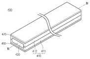
도 3은 제 1 실시예에 따른 광 변환 부재를 도시한 사시도이다.
도 4는 도 3에서 B-B`를 따라서 절단한 단면을 도시한 단면도이다.
도 5 내지 도 8은 광 변환 부재를 제조하는 과정을 도시한 도면들이다.1 is an exploded perspective view showing a liquid crystal display device according to a first embodiment.
FIG. 2 is a cross-sectional view showing a section cut along AA 'in FIG. 1; FIG.
3 is a perspective view showing a light conversion member according to the first embodiment.
FIG. 4 is a cross-sectional view showing a section cut along BB 'in FIG. 3; FIG.
5 to 8 are views illustrating a process of manufacturing the light conversion member.
실시 예의 설명에 있어서, 각 기판, 프레임, 시트, 층 또는 패턴 등이 각 기판, 프레임, 시트, 층 또는 패턴 등의 "상(on)"에 또는 "아래(under)"에 형성되는 것으로 기재되는 경우에 있어, "상(on)"과 "아래(under)"는 "직접(directly)" 또는 "다른 구성요소를 개재하여 (indirectly)" 형성되는 것을 모두 포함한다. 또한 각 구성요소의 상 또는 아래에 대한 기준은 도면을 기준으로 설명한다. 도면에서의 각 구성요소들의 크기는 설명을 위하여 과장될 수 있으며, 실제로 적용되는 크기를 의미하는 것은 아니다.In the description of the embodiments, it is described that each substrate, frame, sheet, layer or pattern, etc., is formed on or "under" of each substrate, frame, sheet, layer or pattern, etc. In the case, “on” and “under” include both being formed “directly” or “indirectly” through other components. In addition, the upper or lower reference of each component is described with reference to the drawings. The size of each component in the drawings may be exaggerated for the sake of explanation and does not mean the size actually applied.
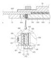
도 1은 제 1 실시예에 따른 액정표시장치를 도시한 분해사시도이다. 도 2는 도 1에서 A-A`를 따라서 절단한 단면을 도시한 단면도이다. 도 3은 제 1 실시예에 따른 광 변환 부재를 도시한 사시도이다. 도 4는 도 3에서 B-B`를 따라서 절단한 단면을 도시한 단면도이다. 도 5 내지 도 8은 광 변환 부재를 제조하는 과정을 도시한 도면들이다.1 is an exploded perspective view showing a liquid crystal display device according to a first embodiment. FIG. 2 is a cross-sectional view illustrating a cross section taken along line AA ′ in FIG. 1. FIG. 3 is a perspective view showing the light conversion member according to the first embodiment. FIG. Fig. 4 is a cross-sectional view showing a section cut along the line B-B 'in Fig. 3; Fig. 5 to 8 are views illustrating a process of manufacturing the light conversion member.
도 1 내지 도 4를 참조하면, 실시예에 따른 액정표시장치는 몰드 프레임(10), 백라이트 어셈블리(20) 및 액정패널(30)을 포함한다.1 to 4, a liquid crystal display device according to an embodiment includes a
상기 몰드 프레임(10)은 상기 백라이트 어셈블리(20) 및 상기 액정패널(30)을 수용한다. 상기 몰드 프레임(10)은 사각 틀 형상을 가지며, 상기 몰드 프레임(10)으로 사용하는 물질의 예로서는 플라스틱 또는 강화 플라스틱 등을 들 수 있다.The
또한, 상기 몰드 프레임(10) 아래에는 상기 몰드 프레임(10)을 감싸며, 상기 백라이트 어셈블리(20)를 지지하는 샤시가 배치될 수 있다. 상기 샤시는 상기 몰드 프레임(10)의 측면에도 배치될 수 있다.In addition, a chassis supporting the
상기 백라이트 어셈블리(20)는 상기 몰드 프레임(10) 내측에 배치되며, 광을 발생시켜 상기 액정패널(30)을 향하여 출사한다. 상기 백라이트 어셈블리(20)는 반사시트(100), 도광판(200), 발광다이오드(300), 광 변환 부재(400), 다수 개의 광학 시트들(500) 및 연성인쇄회로기판(flexible printed circuit board;FPCB)(600)을 포함한다.The
상기 반사시트(100)는 상기 발광다이오드(300)로부터 발생하는 광을 상방으로 반사시킨다.The
상기 도광판(200)은 상기 반사시트(100) 상에 배치되며, 상기 발광다이오드(300)로부터 출사되는 광을 입사받아, 반사, 굴절 및 산란 등을 통해서 상방으로 반사시킨다.The
상기 도광판(200)은 상기 발광다이오드(300)를 향하는 입사면을 포함한다. 즉, 상기 도광판(200)의 측면들 중 상기 발광다이오드(300)를 향하는 면이 입사면이다.The
상기 발광다이오드(300)는 상기 도광판(200)의 측면에 배치된다. 더 자세하게, 상기 발광다이오드(300)는 상기 입사면에 배치된다.The
상기 발광다이오드(300)는 광을 발생시키는 광원이다. 더 자세하게, 상기 발광다이오드(300)는 상기 광 변환 부재(400)를 향하여 광을 출사한다. 또한, 상기 발광다이오드(300)는 광을 발생시키는 발광다이오드 칩(310) 및 상기 발광다이오드 칩(310)을 덮는 충진재(320)를 포함할 수 있다. 또한, 상기 발광다이오드(300)는 상기 발광다이오드 칩(310)을 수용하는 몸체 및 상기 발광다이오드 칩(310)과 전기적으로 연결되는 리드 전극 등을 더 포함할 수 있다.The
상기 발광다이오드(300)는 청색 광을 발생시키는 청색 발광다이오드 또는 자외선을 발생시키는 UV 발광다이오드일 수 있다. 즉, 상기 발광다이오드(300)는 약 430㎚ 내지 약 470㎚ 사이의 파장대를 가지는 청색광 또는 약 300㎚ 내지 약 400㎚ 사이의 파장대를 가지는 자외선을 발생시킬 수 있다.The
상기 발광다이오드(300)는 상기 연성인쇄회로기판(600)에 실장된다. 상기 발광다이오드(300)는 상기 연성인쇄회로기판(600) 아래에 배치된다. 상기 발광다이오드(300)는 상기 연성인쇄회로기판(600)을 통하여 구동신호를 인가받아 구동된다.The
상기 광 변환 부재(400)는 상기 발광다이오드(300) 및 상기 도광판(200) 사이에 개재된다. 상기 광 변환 부재(400)는 상기 도광판(200)의 측면에 접착된다. 더 자세하게, 상기 광 변환 부재(400)는 상기 도광판(200)의 입사면에 부착된다. 또한, 상기 광 변환 부재(400)는 상기 발광다이오드(300)에 접착될 수 있다.The
상기 광 변환 부재(400)는 상기 발광다이오드(300)로부터 출사되는 광을 입사받아, 파장을 변환시킨다. 예를 들어, 상기 광 변환 부재(400)는 상기 발광다이오드(300)로부터 출사되는 청색광을 녹색광 및 적색광으로 변환시킬 수 있다. 즉, 상기 광 변환 부재(400)는 상기 청색광의 일부를 약 520㎚ 내지 약 560㎚ 사이의 파장대를 가지는 녹색광으로 변환시키고, 상기 청색광의 다른 일부를 약 630㎚ 내지 약 660㎚ 사이의 파장대를 가지는 적색광으로 변환시킬 수 있다.The
또한, 상기 광 변환 부재(400)는 상기 발광다이오드(300)로부터 출사되는 자외선을 청색광, 녹색광 및 적색광으로 변환시킬 수 있다. 즉, 상기 광 변환 부재(400)는 상기 자외선의 일부를 약 430㎚ 내지 약 470㎚ 사이의 파장대를 가지는 청색광으로 변환시키고, 상기 자외선의 다른 일부를 약 520㎚ 내지 약 560㎚ 사이의 파장대를 가지는 녹색광으로 변환시키고, 상기 자외선의 또 다른 일부를 약 630㎚ 내지 약 660㎚ 사이의 파장대를 가지는 적색광으로 변환시킬 수 있다.The
이에 따라서, 상기 광 변환 부재(400)를 통과하는 광 및 상기 광 변환 부재(400)에 의해서 변환된 광들은 백색광을 형성할 수 있다. 즉, 청색광, 녹색광 및 적색광이 조합되어, 상기 도광판(200)에는 백색광이 입사될 수 있다.Accordingly, the light passing through the
도 2 내지 도 4에 도시된 바와 같이, 상기 광 변환 부재(400)는 튜브(410), 밀봉부재(420), 다수 개의 광 변환 입자들(430), 호스트(440), 제 1 반사 방지막(460) 및 제 2 반사 방지막(470)을 포함한다.2 to 4, the
상기 튜브(410)는 상기 밀봉부재(420), 상기 광 변환 입자들(430) 및 상기 호스트(440)를 수용한다. 즉, 상기 튜브(410)는 상기 밀봉부재(420), 상기 광 변환 입자들(430) 및 상기 호스트(440)를 수용하는 용기이다. 또한, 상기 튜브(410)는 일 방향으로 길게 연장되는 형상을 가진다.The
상기 튜브(410)는 사각 튜브(410) 형상을 가질 수 있다. 즉, 상기 튜브(410)의 길이 방향에 대하여 수직한 단면은 직사각형 형상을 가질 수 있다. 또한, 상기 튜브(410)의 폭은 약 0.6㎜이고, 상기 튜브(410)의 높이는 약 0.2㎜일 수 있다. 즉, 상기 튜브(410)는 모세관일 수 있다.The
상기 튜브(410)는 입광부(411) 및 출광부(412)를 포함한다. 이때, 상기 입광부(411) 및 상기 출광부(412)는 일체로 형성될 수 있다. 도면에서는 상기 입광부(411) 및 상기 출광부(412)의 경계를 명확하게 도시하였지만, 상기 입광부(411) 및 상기 출광부(412)의 경계는 모호할 수 있다. 또한, 상기 튜브(410)는 상기 입광부(411) 및 상기 출광부(412)로 이루어질 수 있다.The
상기 입광부(411)는 상기 발광다이오드(300)와 마주본다. 더 자세하게, 상기 입광부(411)는 상기 발광다이오드(300)의 출사면에 대향된다. 즉, 상기 입광부(411)는 상기 출광부(412)보다 상기 발광다이오드(300)에 더 가깝다.The
상기 출광부(412)는 상기 도광판(200)과 마주본다. 더 자세하게, 상기 출광부(412)는 상기 도광판(200)의 측면에 대향된다. 즉, 상기 출광부(412)는 상기 입광부(411)보다 상기 도광판(200)에 더 가깝다.The
상기 입광부(411) 및 상기 출광부(412)는 상기 호스트(440)를 사이에 두고 서로 마주본다. 즉, 상기 호스트(440)는 상기 입광부(411) 및 상기 출광부(412) 사이에 개재된다.The
상기 입광부(411) 및 상기 출광부(412)의 굴절율은 서로 다르다. 상기 입광부(411) 및 상기 출광부(412)는 광학적 설계에 따라서 다양한 굴절율을 가질 수 있다. 예를 들어, 상기 입광부(411)의 제 1 굴절율은 상기 출광부(412)의 제 2 굴절율보다 더 낮을 수 있다. 이와는 다르게, 상기 제 1 굴절율은 상기 제 2 굴절율보다 더 클 수 있다.The refractive indices of the
상기 튜브(410)는 투명하다. 상기 튜브(410)로 사용되는 물질의 예로서는 유리 등을 들 수 있다. 즉, 상기 튜브(410)는 유리 모세관일 수 있다. 또한, 상기 입광부(411) 및 상기 출광부(412)는 모두 유리로 형성될 수 있다. 이때, 상기 입광부(411) 및 상기 출광부(412)에는 서로 다른 성분의 유리가 사용되어, 상기 입광부(411) 및 상기 출광부(412)의 굴절율은 서로 다르게 된다.The
상기 밀봉부재(420)는 상기 튜브(410)의 내부에 배치된다. 상기 밀봉부재(420)는 상기 튜브(410)의 끝단에 배치된다. 상기 밀봉부재(420)는 상기 튜브(410)의 내부를 밀봉한다. 상기 밀봉부재(420)는 에폭시계 수지(epoxy resin)를 포함할 수 있다.The sealing
상기 광 변환 입자들(430)은 상기 튜브(410)의 내부에 배치된다. 더 자세하게, 상기 광 변환 입자들(430)은 상기 호스트(440)에 균일하게 분산되고, 상기 호스트(440)는 상기 튜브(410)의 내부에 배치된다.The photo-
상기 광 변환 입자들(430)은 상기 발광다이오드(300)로부터 출사되는 광의 파장을 변환시킨다. 상기 광 변환 입자들(430)은 상기 발광다이오드(300)로부터 출사되는 광을 입사받아, 파장을 변환시킨다. 예를 들어, 상기 광 변환 입자들(430)은 상기 발광다이오드(300)로부터 출사되는 청색광을 녹색광 및 적색광으로 변환시킬 수 있다. 즉, 상기 광 변환 입자들(430) 중 일부는 상기 청색광을 약 520㎚ 내지 약 560㎚ 사이의 파장대를 가지는 녹색광으로 변환시키고, 상기 광 변환 입자들(430) 중 다른 일부는 상기 청색광을 약 630㎚ 내지 약 660㎚ 사이의 파장대를 가지는 적색광으로 변환시킬 수 있다.The
이와는 다르게, 상기 광 변환 입자들(430)은 상기 발광다이오드(300)로부터 출사되는 자외선을 청색광, 녹색광 및 적색광으로 변환시킬 수 있다. 즉, 상기 광 변환 입자들(430) 중 일부는 상기 자외선을 약 430㎚ 내지 약 470㎚ 사이의 파장대를 가지는 청색광으로 변환시키고, 상기 광 변환 입자들(430) 중 다른 일부는 상기 자외선을 약 520㎚ 내지 약 560㎚ 사이의 파장대를 가지는 녹색광으로 변환시킬 수 있다. 또한, 상기 광 변환 입자들(430) 중 또 다른 일부는 상기 자외선을 약 630㎚ 내지 약 660㎚ 사이의 파장대를 가지는 적색광으로 변환시킬 수 있다.Alternatively, the
즉, 상기 발광다이오드(300)가 청색광을 발생시키는 청색 발광다이오드인 경우, 청색광을 녹색광 및 적색광으로 각각 변환시키는 광 변환 입자들(430)이 사용될 수 있다. 이와는 다르게, 상기 발광다이오드(300)가 자외선을 발생시키는 UV 발광다이오드인 경우, 자외선을 청색광, 녹색광 및 적색광으로 각각 변환시키는 광 변환 입자들(430)이 사용될 수 있다.That is, when the
상기 광 변환 입자들(430)은 다수 개의 양자점(QD, Quantum Dot)들일 수 있다. 상기 양자점은 코어 나노 결정 및 상기 코어 나노 결정을 둘러싸는 껍질 나노 결정을 포함할 수 있다. 또한, 상기 양자점은 상기 껍질 나노 결정에 결합되는 유기 리간드를 포함할 수 있다. 또한, 상기 양자점은 상기 껍질 나노 결정을 둘러싸는 유기 코팅층을 포함할 수 있다.The
상기 껍질 나노 결정은 두 층 이상으로 형성될 수 있다. 상기 껍질 나노 결정은 상기 코어 나노 결정의 표면에 형성된다. 상기 양자점은 상기 코어 나오 결정으로 입광되는 빛의 파장을 껍질층을 형성하는 상기 껍질 나노 결정을 통해서 파장을 길게 변환시키고 빛의 효율을 증가시길 수 있다.The shell nanocrystals may be formed of two or more layers. The shell nanocrystals are formed on the surface of the core nanocrystals. The quantum dot may convert the wavelength of the light incident on the core core crystal into a long wavelength through the shell nanocrystals forming the shell layer and increase the light efficiency.
상기 양자점은 Ⅱ족 화합물 반도체, Ⅲ족 화합물 반도체, Ⅴ족 화합물 반도체 그리고 VI족 화합물 반도체 중에서 적어도 한가지 물질을 포함할 수 있다. 보다 상세하게, 상기 코어 나노 결정은 Cdse, InGaP, CdTe, CdS, ZnSe, ZnTe, ZnS, HgTe 또는 HgS를 포함할 수 있다. 또한, 상기 껍질 나노 결정은 CuZnS, CdSe, CdTe, CdS, ZnSe, ZnTe, ZnS, HgTe 또는 HgS를 포함할 수 있다. 상기 양자점의 지름은 1 nm 내지 10 nm일 수 있다.The quantum dot may include at least one of a group II compound semiconductor, a group III compound semiconductor, a group V compound semiconductor, and a group VI compound semiconductor. More specifically, the core nanocrystals may include Cdse, InGaP, CdTe, CdS, ZnSe, ZnTe, ZnS, HgTe or HgS. The shell nanocrystals may include CuZnS, CdSe, CdTe, CdS, ZnSe, ZnTe, ZnS, HgTe or HgS. The diameter of the quantum dot may be 1 nm to 10 nm.
상기 양자점에서 방출되는 빛의 파장은 상기 양자점의 크기 또는 합성 과정에서의 분자 클러스터 화합물(molecular cluster compound)와 나노입자 전구체 (precurser)의 몰분율 (molar ratio)에 따라 조절이 가능하다. 상기 유기 리간드는 피리딘(pyridine), 메르캅토 알콜(mercapto alcohol), 티올(thiol), 포스핀(phosphine) 및 포스핀 산화물(phosphine oxide) 등을 포함할 수 있다. 상기 유기 리간드는 합성 후 불안정한 양자점을 안정화시키는 역할을 한다. 합성 후에 댕글링 본드(dangling bond)가 외곽에 형성되며, 상기 댕글링 본드 때문에, 상기 양자점이 불안정해 질 수도 있다. 그러나, 상기 유기 리간드의 한 쪽 끝은 비결합 상태이고, 상기 비결합된 유기 리간드의 한 쪽 끝이 댕글링 본드와 결합해서, 상기 양자점을 안정화 시킬 수 있다.The wavelength of light emitted from the quantum dots can be controlled by the size of the quantum dots or the molar ratio of the molecular cluster compound and the nanoparticle precursor in the synthesis process. The organic ligand may include pyridine, mercapto alcohol, thiol, phosphine, phosphine oxide, and the like. The organic ligands serve to stabilize unstable quantum dots after synthesis. After synthesis, a dangling bond is formed on the outer periphery, and the quantum dots may become unstable due to the dangling bonds. However, one end of the organic ligand is in an unbonded state, and one end of the unbound organic ligand bonds with the dangling bond, thereby stabilizing the quantum dot.
특히, 상기 양자점은 그 크기가 빛, 전기 등에 의해 여기되는 전자와 정공이 이루는 엑시톤(exciton)의 보어 반경(Bohr raidus)보다 작게 되면 양자구속효과가 발생하여 띄엄띄엄한 에너지 준위를 가지게 되며 에너지 갭의 크기가 변화하게 된다. 또한, 전하가 양자점 내에 국한되어 높은 발광효율을 가지게 된다.Particularly, when the quantum dot has a size smaller than the Bohr radius of an exciton formed by electrons and holes excited by light, electricity or the like, a quantum confinement effect is generated to have a staggering energy level and an energy gap The size of the image is changed. Further, the charge is confined within the quantum dots, so that it has a high luminous efficiency.
이러한 상기 양자점은 일반적 형광 염료와 달리 입자의 크기에 따라 형광파장이 달라진다. 즉, 입자의 크기가 작아질수록 짧은 파장의 빛을 내며, 입자의 크기를 조절하여 원하는 파장의 가시광선영역의 형광을 낼 수 있다. 또한, 일반적 염료에 비해 흡광계수(extinction coefficient)가 100~1000배 크고 양자효율(quantum yield)도 높으므로 매우 센 형광을 발생한다.Unlike general fluorescent dyes, the quantum dots vary in fluorescence wavelength depending on the particle size. That is, as the size of the particle becomes smaller, it emits light having a shorter wavelength, and the particle size can be adjusted to produce fluorescence in a visible light region of a desired wavelength. In addition, since the extinction coefficient is 100 to 1000 times higher than that of a general dye, and the quantum yield is also high, it produces very high fluorescence.
상기 양자점은 화학적 습식방법에 의해 합성될 수 있다. 여기에서, 화학적 습식방법은 유기용매에 전구체 물질을 넣어 입자를 성장시키는 방법으로서, 화학적 습식방법에 의해서, 상기 양자점이 합성될 수 있다.The quantum dot can be synthesized by a chemical wet process. Here, the chemical wet method is a method of growing particles by adding a precursor material to an organic solvent, and the quantum dots can be synthesized by a chemical wet method.
상기 호스트(440)는 상기 광 변환 입자들(430)을 둘러싼다. 즉, 상기 호스트(440)는 상기 광 변환 입자들(430)을 균일하게 내부에 분산시킨다. 상기 호스트(440)는 폴리머로 구성될 수 있다. 상기 호스트(440)는 투명하다. 즉, 상기 호스트(440)는 투명한 폴리머로 형성될 수 있다.The
상기 호스트(440)는 상기 튜브(410) 내부에 배치된다. 즉, 상기 호스트(440)는 전체적으로 상기 튜브(410) 내부에 채워진다. 상기 호스트(440)는 상기 튜브(410)의 내면에 밀착될 수 있다.The
상기 밀봉부재(420) 및 상기 호스트(440) 사이에는 공기층(450)이 형성된다. 상기 공기층(450)에는 질소로 채워진다. 상기 공기층(450)은 상기 밀봉부재(420) 및 상기 호스트(440) 사이에서 완충 기능을 수행한다.An
상기 제 1 반사 방지막(460)은 상기 튜브(410)의 외부 표면에 배치된다. 더 자세하게, 상기 제 1 반사 방지막(460)은 상기 입광부(411)에 배치된다. 상기 제 1 반사 방지막(460)은 상기 튜브(410) 및 상기 발광다이오드(300) 사이에 배치된다. 더 자세하게, 상기 제 1 반사 방지막(460)은 상기 입광부(411)의 외부 표면에 코팅된다.The first
상기 제 1 반사 방지막(460)은 상기 발광다이오드(300)로부터 입사되는 광의 반사를 감소시킨다. 상기 제 1 반사 방지막(460)은 투명하다. 상기 제 1 반사 방지막(460)으로 사용되는 물질의 예로서는 실리콘 옥사이드(silicon oxide) 또는 실리콘 나이트라이드(silicon nitride)와 같은 실리콘 산화물 등을 들 수 있다. 또한, 상기 제 1 반사 방지막(460)으로 마그네슘 플루오라이드(magnesium fluoride, MgF2) 등이 사용될 수 있다. 광학적 설계에 따라서, 상기 제 1 반사 방지막(460)으로 적절한 굴절율을 가지는 물질이 사용될 수 있다.The first
마찬가지로, 광학적 설계에 따라서, 상기 제 1 반사 방지막(460)의 두께는 달라질 수 있다. 예를 들어, 상기 제 1 반사 방지막(460)의 두께는 약 100Å 내지 약 800Å일 수 있다.Similarly, depending on the optical design, the thickness of the first
상기 제 2 반사 방지막(470)은 상기 튜브(410)의 외부 표면에 배치된다. 더 자세하게, 상기 제 2 반사 방지막(470)은 상기 출광부(412)에 배치된다. 즉, 상기 제 2 반사 방지막(470)은 상기 튜브(410) 및 상기 도광판(200) 사이에 배치된다. 더 자세하게, 상기 제 2 반사 방지막(470)은 상기 출광부(412)의 외부 표면에 코팅된다.The second
상기 제 2 반사 방지막(470)은 상기 튜브(410)로부터 출사되는 광의 출광 효율을 증가시킨다. 상기 제 2 반사 방지막(470)은 투명하다. 상기 제 2 반사 방지막(470)으로 사용되는 물질의 예로서는 실리콘 옥사이드 또는 실리콘 나이트라이드와 같은 실리콘 산화물 등을 들 수 있다. 또한, 상기 제 2 반사 방지막(470)으로 마그네슘 플루오라이드 등이 사용될 수 있다. 광학적 설계에 따라서, 상기 제 2 반사 방지막(470)으로 적절한 굴절율을 가지는 물질이 사용될 수 있다.The second
마찬가지로, 광학적 설계에 따라서, 상기 제 2 반사 방지막(470)의 두께는 달라질 수 있다. 예를 들어, 상기 제 2 반사 방지막(470)의 두께는 약 100Å 내지 약 800Å일 수 있다.Similarly, depending on the optical design, the thickness of the second
도 2를 참조하면, 상기 광 변환 부재(400)는 상기 발광다이오드(300)에 접착된다. 상기 광 변환 부재(400) 및 상기 발광다이오드(300) 사이에는 제 1 접착층(101)이 개재된다. 상기 광 변환 부재(400)는 상기 제 1 접착층(101)을 통하여, 상기 발광다이오드(300)의 출사면에 접착될 수 있다.Referring to FIG. 2, the
상기 광 변환 부재(400)는 상기 제 1 접착층(101)에 밀착된다. 더 자세하게, 상기 제 1 반사 방지막(460)은 상기 제 1 접착층(101)에 밀착된다. 또한, 상기 제 1 접착층(101)은 상기 발광다이오드(300)에 밀착된다. 더 자세하게, 상기 제 1 접착층(101)은 상기 충진재(320)에 밀착된다. 이에 따라서, 상기 발광다이오드(300) 및 상기 광 변환 부재(400) 사이에는 공기층이 존재하지 않는다.The
상기 제 1 접착층(101)은 투명하다. 상기 제 1 접착층(101)으로 사용되는 물질의 예로서는 에폭시계 수지 또는 아크릴계 수지 등을 들 수 있다.The first
또한, 상기 광 변환 부재(400)는 상기 도광판(200)에 접착된다. 상기 광 변환 부재(400) 및 상기 도광판(200) 사이에는 제 2 접착층(201)이 개재되고, 상기 광 변환 부재(400)는 상기 제 2 접착층(201)을 통하여, 상기 도광판(200)의 측면에 접착된다.In addition, the
상기 광 변환 부재(400)는 상기 제 2 접착층(201)에 밀착된다. 더 자세하게, 상기 제 2 반사 방지막(470)은 상기 제 2 접착층(201)에 밀착된다. 또한, 상기 제 2 접착층(201)은 상기 도광판(200)에 밀착된다. 즉, 상기 제 1 접착층(101)은 상기 도광판(200)의 측면에 밀착된다. 이에 따라서, 상기 광 변환 부재(400) 및 상기 도광판(200) 사이에는 공기층이 존재하지 않게 된다.The
상기 제 2 접착층(201)은 투명하다. 상기 제 2 접착층(201)으로 사용되는 물질의 예로서는 에폭시계 수지 또는 아크릴계 수지 등을 들 수 있다.The second
이와 같이, 상기 제 1 접착층(101) 및 상기 제 2 접착층(201)에 의해서, 상기 발광다이오드(300)로부터 출사되는 광은 공기층을 통과하지 않고, 상기 광 변환 부재(400)를 통과하여, 상기 도광판(200)에 입사될 수 있다.As described above, the light emitted from the
상기 발광다이오드 칩(310)에 의해서 발생되는 광은 상기 충진재(320), 상기 제 1 접착층(101), 상기 제 1 반사 방지막(460), 상기 입광부(411), 상기 호스트(440), 상기 출광부(412), 상기 제 2 반사 방지막(470) 및 상기 제 2 접착층(201)을 통과하여, 상기 도광판(200)에 입사된다.Light generated by the light emitting
따라서, 상기 도광판(200)으로의 입광 효율을 향상시키기 위해서, 상기 충진재(320), 상기 제 1 접착층(101), 상기 제 1 반사 방지막(460), 상기 입광부(411), 상기 호스트(440), 상기 출광부(412), 상기 제 2 반사 방지막(470), 상기 제 2 접착층(201) 및 상기 도광판(200)의 굴절율이 적절하게 조절되어야 한다.Therefore, in order to improve light incident efficiency to the
상기 튜브(410)는 상기 입광부(411) 및 상기 출광부(412)의 굴절율을 서로 다르도록 설계될 수 있으므로, 본 실시예에 따른 액정표시장치는 향상된 휘도를 가질 수 있다.Since the
예를 들어, 상기 충진재(320), 상기 제 1 접착층(101), 상기 제 1 반사 방지막(460), 상기 입광부(411), 상기 호스트(440), 상기 출광부(412), 상기 제 2 반사 방지막(470), 상기 제 2 접착층(201) 및 상기 도광판(200)의 순으로 굴절율이 커질 수 있다.For example, the
즉, 상기 출광부(412)의 굴절율은 상기 도광판(200)의 굴절율보다 더 낮을 수 있다. 또한, 상기 입광부(411)의 굴절율은 상기 출광부(412)의 굴절율보다 더 낮을 수 있다. 또한, 상기 제 1 반사 방지막(460)의 굴절율은 상기 입광부(411)의 굴절율보다 더 낮을 수 있다. 또한, 상기 제 2 반사 방지막(470)의 굴절율은 상기 출광부(412)의 굴절율보다 더 클 수 있다. 또한, 상기 제 1 접착층(101)의 굴절율은 상기 입광부(411)의 굴절율보다 더 낮을 수 있다. 또한, 상기 제 2 접착층(201)의 굴절율은 상기 출광부(412)의 굴절율보다 더 클 수 있다.That is, the refractive index of the
이와는 다르게, 상기 충진재(320), 상기 제 1 접착층(101), 상기 제 1 반사 방지막(460), 상기 입광부(411), 상기 호스트(440), 상기 출광부(412), 상기 제 2 반사 방지막(470), 상기 제 2 접착층(201) 및 상기 도광판(200) 순으로 굴절율이 작아질 수 있다.Alternatively, the
또한, 상기 입광부(411)의 굴절율은 상기 호스트(440)의 굴절율 및 상기 충진재(320)의 굴절율 사이일 수 있다. 더 자세하게, 상기 입광부(411)의 굴절율은 상기 제 1 반사 방지막(460) 및 상기 호스트(440)의 굴절율 사이일 수 있다.In addition, the refractive index of the
또한, 상기 출광부(412)의 굴절율은 상기 호스트(440)의 굴절율 및 상기 도광판(200)의 굴절율 사이일 수 있다. 더 자세하게, 상기 출광부(412)의 굴절율은 상기 호스트(440)의 굴절율 및 상기 제 2 반사 방지막(470)의 굴절율 사이일 수 있다.In addition, the refractive index of the
또한, 상기 호스트(440)의 굴절율은 상기 입광부(411)의 굴절율 및 상기 출광부(412)의 굴절율 사이일 수 있다.In addition, the refractive index of the
또한, 상기 제 1 반사 방지막(460)의 굴절율은 상기 충진재(320)의 굴절율 및 상기 입광부(411)의 굴절율 사이일 수 있다. 상기 제 1 반사 방지막(460)의 굴절율은 상기 제 1 접착층(101)의 굴절율 및 상기 입광부(411)의 굴절율 사이일 수 있다.In addition, the refractive index of the first
또한, 상기 제 2 반사 방지막(470)의 굴절율은 상기 출광부(412)의 굴절율 및 상기 도광판(200)의 굴절율 사이일 수 있다. 더 자세하게, 상기 제 2 반사 방지막(470)의 굴절율은 상기 출광부(412) 및 상기 제 2 접착층(201)의 굴절율 사이일 수 있다.In addition, the refractive index of the second
또한, 상기 제 1 접착층(101)의 굴절율은 상기 충진재(320)의 굴절율 및 상기 입광부(411)의 굴절율 사이일 수 있다. 더 자세하게, 상기 제 1 접착층(101)의 굴절율은 상기 충진재(320)의 굴절율 및 상기 제 1 반사 방지막(460)의 굴절율 사이일 수 있다.In addition, the refractive index of the first
또한, 상기 제 2 접착층(201)의 굴절율은 상기 출광부(412)의 굴절율 및 상기 도광판(200)의 굴절율 사이일 수 있다. 더 자세하게, 상기 제 2 접착층(201)의 굴절율은 상기 제 2 반사 방지막(470)의 굴절율 및 상기 도광판(200)의 굴절율 사이일 수 있다.In addition, the refractive index of the second
결과적으로, 광이 통과되는 층들(320, 101, 460, 411, 440, 412, 470, 201, 200)의 굴절율은, 서로 인접하는 층들 사이의 굴절율의 차이가 최소화되도록, 설계될 수 있다.As a result, the refractive indices of the
이와 같이, 다양한 방법으로 상기 광이 통과되는 층들(320, 101, 460, 411, 440, 412, 470, 201, 200)의 굴절율이 적절하게 조절되고, 이에 따라서, 실시예에 따른 액정 표시장치는 높은 휘도를 가질 수 있다.As such, the refractive indices of the
상기 광학 시트들(500)은 상기 도광판(200) 상에 배치된다. 상기 광학 시트들(500)은 통과하는 광의 특성을 향상시킨다.The
상기 연성인쇄회로기판(600)은 상기 발광다이오드(300)에 전기적으로 연결된다. 상기 발광다이오드(300)를 실장할 수 있다. 상기 연성인쇄회로기판(600)은 연성인쇄회로기판이며, 상기 몰드 프레임(10) 내측에 배치된다. 상기 연성인쇄회로기판(600)은 상기 도광판(200) 상에 배치된다.The flexible printed
상기 몰드 프레임(10) 및 상기 백라이트 어셈블리(20)에 의해서 백라이트 유닛이 구성된다. 즉, 상기 백라이트 유닛은 상기 몰드 프레임(10) 및 상기 백라이트 어셈블리(20)를 포함한다.The
상기 액정패널(30)은 상기 몰드 프레임(10) 내측에 배치되고, 상기 광학시트들(500)상에 배치된다.The
상기 액정패널(30)은 통과하는 광의 세기를 조절하여 영상을 표시한다. 즉, 상기 액정패널(300)은 영상을 표시하는 표시패널이다. 상기 액정패널(30)은 TFT기판, 컬러필터기판, 두 기판들 사이에 개재되는 액정층 및 편광필터들을 포함한다.The
도 5 내지 도 8은 상기 광 변환 부재(400)를 제조하는 과정을 도시한 도면들이다. 상기 광 변환 부재(400)는 다음과 같은 방법에 의해서 형성될 수 있다.5 to 8 illustrate a process of manufacturing the
도 5를 참조하면, 입광부(411) 및 출광부(412)를 포함하는 튜브(410)가 형성된다. 더 자세하게, 상기 입광부(411)는 제 1 용융 유리(410a)가 인상되어 형성되고, 상기 출광부(412)는 제 2 용융 유리(410b)가 인상되어 형성될 수 있다.Referring to FIG. 5, a
즉, 상기 튜브(410)는 상기 제 1 용융 유리(410a) 및 상기 제 2 용융 유리(410b)가 동시에 인상 및 냉각되어, 형성될 수 있다. 이때, 상기 제 1 용융 유리(410a) 및 상기 제 2 용융 유리(410b)는 서로 다른 성분을 포함할 수 있다.That is, the
도 6을 참조하면, 수지 조성물(441)에 상기 광 변환 입자들(430)이 균일하게 분산된다. 상기 수지 조성물(441)은 투명하다. 상기 수지 조성물(441)은 광 경화성을 가질 수 있다.Referring to FIG. 6, the
이후, 상기 튜브(410)의 내부는 감압되고, 상기 광 변환 입자들(430)이 분산된 수지 조성물(441)에 상기 튜브(410)의 입구가 잠기고, 주위의 압력이 상승된다. 이에 따라서, 상기 광 변환 입자들(430)이 분산된 수지 조성물(441)은 상기 튜브(410) 내부로 유입된다.Thereafter, the inside of the
도 7을 참조하면, 상기 튜브(410) 내로 유입된 수지 조성물(441)의 일부가 제거되고, 상기 튜브(410)의 입구 부분이 비워진다. 이후, 상기 튜브(410) 내로 유입된 수지 조성물(441)은 자외선 등에 의해서 경화되고, 상기 호스트(440)가 형성된다.Referring to FIG. 7, a portion of the
도 8을 참조하면, 상기 튜브(410)의 입구 부분에 에폭시계 수지 조성물이 유입된다. 이후, 유입된 에폭시계 수지 조성물은 경화되고, 상기 밀봉부재(420)가 형성된다. 상기 밀봉부재(420)가 형성되는 공정은 질소 분위기에서 진행되고, 이에 따라서, 질소를 포함하는 공기층(450)이 상기 밀봉부재(420) 및 상기 호스트(440) 사이에 형성될 수 있다.Referring to FIG. 8, an epoxy resin composition flows into an inlet portion of the
도 9를 참조하면, 진공 증착 등의 공정에 의해서, 상기 입광부(411)에 상기 제 1 반사 방지막(460)이 형성된다. 또한, 진공 증착 등의 공정으로, 상기 출광부(412)에 상기 제 2 반사 방지막(470)이 형성된다.Referring to FIG. 9, the
상기 제 1 반사 방지막(460) 및 상기 제 2 반사 방지막(470)은 상기 튜브(410)가 형성된 후, 바로 형성될 수 있다. 즉, 상기 제 1 반사 방지막(460) 및 상기 제 2 반사 방지막(470)은 상기 수지 조성물(441)이 상기 튜브(410) 내로 유입되기 전에 형성될 수 있다.The first
이와 같은 방식으로, 상기 광 변환 부재(400)가 형성될 수 있다.In this manner, the
앞서 설명한 바와 같이, 상기 튜브(410)는 굴절율이 서로 다른 상기 입광부(411) 및 상기 출광부(412)를 포함한다. 이때, 상기 입광부(411) 및 상기 출광부(412)의 굴절율은 실시예에 따른 광 변환 부재(400)가 최적의 입광 효율 및 출광 효율을 가지도록 조절될 수 있다.As described above, the
이에 따라서, 상기 광 변환 부재(400)는 굴절율이 서로 다른 부분들(411, 412)을 포함하는 상기 튜브(410)를 사용하여, 반사에 의한 광 손실을 줄이고, 향상된 입광 효율 및 출광 효율을 구현할 수 있다.Accordingly, the
또한, 상기 광 변환 부재(400)는 상기 제 1 반사 방지막(460) 및 상기 제 2 반사 방지막(470)을 사용하여, 반사에 의한 광 손실을 줄이고, 입광 효율 및 출광 효율을 향상시킬 수 있다.In addition, the
이에 따라서, 실시예에 따른 액정 표시장치는 향상된 광학적 특성을 가지고, 향상된 휘도를 가질 수 있다.Accordingly, the liquid crystal display according to the embodiment may have improved optical characteristics and improved luminance.
또한, 이상에서 실시예들에 설명된 특징, 구조, 효과 등은 본 발명의 적어도 하나의 실시예에 포함되며, 반드시 하나의 실시예에만 한정되는 것은 아니다. 나아가, 각 실시예에서 예시된 특징, 구조, 효과 등은 실시예들이 속하는 분야의 통상의 지식을 가지는 자에 의해 다른 실시예들에 대해서도 조합 또는 변형되어 실시 가능하다. 따라서 이러한 조합과 변형에 관계된 내용들은 본 발명의 범위에 포함되는 것으로 해석되어야 할 것이다.In addition, the features, structures, effects and the like described in the embodiments are included in at least one embodiment of the present invention, and are not necessarily limited to only one embodiment. Furthermore, the features, structures, effects, and the like illustrated in each embodiment may be combined or modified with respect to other embodiments by those skilled in the art to which the embodiments belong. Therefore, it should be understood that the present invention is not limited to these combinations and modifications.
이상에서 실시예를 중심으로 설명하였으나 이는 단지 예시일 뿐 본 발명을 한정하는 것이 아니며, 본 발명이 속하는 분야의 통상의 지식을 가진 자라면 본 실시예의 본질적인 특성을 벗어나지 않는 범위에서 이상에 예시되지 않은 여러 가지의 변형과 응용이 가능함을 알 수 있을 것이다. 예를 들어, 실시예에 구체적으로 나타난 각 구성 요소는 변형하여 실시할 수 있는 것이다. 그리고 이러한 변형과 응용에 관계된 차이점들은 첨부된 청구 범위에서 규정하는 본 발명의 범위에 포함되는 것으로 해석되어야 할 것이다.While the present invention has been particularly shown and described with reference to exemplary embodiments thereof, it is to be understood that the invention is not limited to the disclosed exemplary embodiments, but, on the contrary, It will be understood that various modifications and applications are possible. For example, each component specifically shown in the embodiments can be modified and implemented. It is to be understood that all changes and modifications that come within the meaning and range of equivalency of the claims are therefore intended to be embraced therein.
Claims (15)
Translated fromKorean상기 튜브 내측에 배치되는 호스트; 및
상기 호스트에 분산되는 다수 개의 광 변환 입자들을 포함하고,
상기 튜브는
제 1 굴절율을 가지는 입광부;
상기 제 1 굴절율과 다른 제 2 굴절율을 가지는 출광부; 및
상기 튜브의 일 끝단에 배치되는 밀봉부재를 포함하고,
상기 광 변환 입자는 양자점(QD, Quantum Dot)을 포함하는 광 변환 부재.tube;
A host disposed inside the tube; And
It includes a plurality of light conversion particles dispersed in the host,
The tube is
A light incident part having a first refractive index;
A light emitting part having a second refractive index different from the first refractive index; And
A sealing member disposed at one end of the tube,
The light conversion particle includes a quantum dot (QD).
상기 출광부에 배치되는 제 2 반사 방지막을 포함하는 광 변환 부재.The display apparatus of claim 1, further comprising: a first anti-reflection film disposed on the light incident part; And
And a second anti-reflection film disposed on the light exit portion.
상기 제 2 반사 방지막의 굴절율은 상기 제 2 굴절율보다 더 큰 광 변환 부재.The method of claim 5, wherein the refractive index of the first anti-reflection film is lower than the first refractive index,
And the refractive index of the second anti-reflection film is greater than the second refractive index.
상기 도광판 상에 배치되는 표시패널;
상기 도광판의 측면에 배치되는 광원; 및
상기 광원 및 상기 도광판 사이에 개재되는 광 변환 부재를 포함하고,
상기 광 변환 부재는
호스트;
상기 호스트 내에 분산되는 광 변환 입자들; 및
상기 호스트를 둘러싸는 튜브; 및
상기 튜브의 일 끝단에 배치되는 밀봉부재를 포함하고,
상기 튜브는
제 1 굴절율을 가지는 입광부; 및
상기 제 1 굴절율과 다른 제 2 굴절율을 가지는 출광부를 포함하고,
상기 광 변환 입자는 양자점을 포함하는 표시장치.Light guide plate;
A display panel on the light guide plate;
A light source disposed on a side of the light guide plate; And
A light conversion member interposed between the light source and the light guide plate,
The light conversion member
Host;
Light converting particles dispersed in the host; And
A tube surrounding the host; And
A sealing member disposed at one end of the tube,
The tube is
A light incident part having a first refractive index; And
A light emitting part having a second refractive index different from the first refractive index,
The light conversion particle includes a quantum dot.
상기 출광부 및 상기 도광판에 접착되는 제 2 접착층을 포함하고,
상기 제 1 굴절율은 상기 제 1 접착층의 굴절율보다 더 크고,
상기 제 2 굴절율은 상기 제 2 접착층의 굴절율보다 더 낮은 표시장치.The semiconductor device of claim 10, further comprising: a first adhesive layer adhered to the light incident part and the light source; And
A second adhesive layer adhered to the light emitting part and the light guide plate;
The first refractive index is greater than the refractive index of the first adhesive layer,
And the second refractive index is lower than the refractive index of the second adhesive layer.
광을 발생시키는 발광다이오드 칩; 및
상기 발광다이오드 칩을 덮는 충진재를 포함하고,
상기 제 1 굴절율은 상기 충진재의 굴절율보다 더 크고,
상기 제 2 굴절율은 상기 제 1 굴절율보다 더 큰 표시장치.The method of claim 10, wherein the light source
Light emitting diode chip for generating light; And
A filler covering the light emitting diode chip;
The first refractive index is greater than the refractive index of the filler,
And the second refractive index is greater than the first refractive index.
Priority Applications (4)
| Application Number | Priority Date | Filing Date | Title |
|---|---|---|---|
| KR1020110009833AKR101210066B1 (en) | 2011-01-31 | 2011-01-31 | Light conversion member and display device having the same |
| US13/982,916US9581748B2 (en) | 2011-01-31 | 2011-11-30 | Optical member and display device including the same |
| PCT/KR2011/009232WO2012105746A1 (en) | 2011-01-31 | 2011-11-30 | Optical member and display device including the same |
| US15/407,944US9720159B2 (en) | 2011-01-31 | 2017-01-17 | Optical member and display device including the same |
Applications Claiming Priority (1)
| Application Number | Priority Date | Filing Date | Title |
|---|---|---|---|
| KR1020110009833AKR101210066B1 (en) | 2011-01-31 | 2011-01-31 | Light conversion member and display device having the same |
Publications (2)
| Publication Number | Publication Date |
|---|---|
| KR20120088470A KR20120088470A (en) | 2012-08-08 |
| KR101210066B1true KR101210066B1 (en) | 2012-12-07 |
Family
ID=46602932
Family Applications (1)
| Application Number | Title | Priority Date | Filing Date |
|---|---|---|---|
| KR1020110009833AActiveKR101210066B1 (en) | 2011-01-31 | 2011-01-31 | Light conversion member and display device having the same |
Country Status (3)
| Country | Link |
|---|---|
| US (2) | US9581748B2 (en) |
| KR (1) | KR101210066B1 (en) |
| WO (1) | WO2012105746A1 (en) |
Cited By (1)
| Publication number | Priority date | Publication date | Assignee | Title |
|---|---|---|---|---|
| US10488709B2 (en) | 2014-06-25 | 2019-11-26 | Samsung Display Co., Ltd. | Fluorescent sheet and light unit and liquid crystal display including the same |
Families Citing this family (13)
| Publication number | Priority date | Publication date | Assignee | Title |
|---|---|---|---|---|
| KR101508284B1 (en) | 2009-12-15 | 2015-04-06 | 엘지이노텍 주식회사 | Backlight unit using quantum dot and liquid crystal display device including the same |
| RU2633924C2 (en)* | 2012-08-31 | 2017-10-19 | Филипс Лайтинг Холдинг Б.В. | Lighting device on basis of heat-conductive sheet with light-diffusing particles |
| US9551826B2 (en)* | 2014-01-27 | 2017-01-24 | Shenzhen China Star Optoelectronics Technology Co., Ltd. | LCD with backlight module having quantum dot unit and frame |
| KR102160919B1 (en)* | 2014-02-05 | 2020-10-06 | 삼성디스플레이 주식회사 | Backlight assembly and display divece having the same |
| KR20150093890A (en)* | 2014-02-07 | 2015-08-19 | 삼성디스플레이 주식회사 | Quantum dot filling tube, quantum dot filling tube manafacturing method and display device having the same |
| KR102232783B1 (en)* | 2014-10-16 | 2021-03-29 | 삼성디스플레이 주식회사 | Backlight unit and liquid crystal display device including same |
| US9958596B2 (en) | 2014-11-12 | 2018-05-01 | E Ink Holdings Inc. | Display device, multilayer light guide plate structure and front light module |
| KR101686737B1 (en)* | 2015-04-30 | 2016-12-14 | 엘지전자 주식회사 | Light conversion plate, light emitting diode package, backlight unit and display device comprising the same |
| KR102689844B1 (en)* | 2017-01-23 | 2024-07-29 | 삼성디스플레이 주식회사 | Wavelength conversion member and backlight unit including the same |
| KR102433161B1 (en)* | 2017-08-18 | 2022-08-17 | 삼성디스플레이 주식회사 | Optical member and display including the same |
| US10495925B2 (en)* | 2017-12-28 | 2019-12-03 | Huizhou China Star Optoelectronics Technology Co., Ltd. | Backlight module and display device |
| JP6947989B2 (en)* | 2019-03-28 | 2021-10-13 | 日亜化学工業株式会社 | Linear light source and planar light emitting device |
| JP2024077811A (en)* | 2022-11-29 | 2024-06-10 | 株式会社ジャパンディスプレイ | Display device |
Citations (2)
| Publication number | Priority date | Publication date | Assignee | Title |
|---|---|---|---|---|
| JP2004303441A (en)* | 2003-03-28 | 2004-10-28 | Minebea Co Ltd | Planar lighting system |
| KR100867066B1 (en) | 2000-09-25 | 2008-11-04 | 미츠비시 레이온 가부시키가이샤 | Surface light source device |
Family Cites Families (107)
| Publication number | Priority date | Publication date | Assignee | Title |
|---|---|---|---|---|
| JP3931355B2 (en) | 1995-09-06 | 2007-06-13 | 日亜化学工業株式会社 | Planar light source |
| TW383508B (en) | 1996-07-29 | 2000-03-01 | Nichia Kagaku Kogyo Kk | Light emitting device and display |
| US6608332B2 (en) | 1996-07-29 | 2003-08-19 | Nichia Kagaku Kogyo Kabushiki Kaisha | Light emitting device and display |
| US20050146258A1 (en) | 1999-06-02 | 2005-07-07 | Shimon Weiss | Electronic displays using optically pumped luminescent semiconductor nanocrystals |
| JP4573946B2 (en) | 2000-05-16 | 2010-11-04 | 株式会社きもと | Light diffusing sheet |
| US6723478B2 (en) | 2000-12-08 | 2004-04-20 | Hitachi, Ltd. | Color filter and liquid crystal display provided therewith |
| US20030066998A1 (en) | 2001-08-02 | 2003-04-10 | Lee Howard Wing Hoon | Quantum dots of Group IV semiconductor materials |
| JP2003255562A (en) | 2002-03-04 | 2003-09-10 | Sharp Corp | Pattern forming method and display device using the method |
| TWI292961B (en) | 2002-09-05 | 2008-01-21 | Nichia Corp | Semiconductor device and an optical device using the semiconductor device |
| JP4072632B2 (en) | 2002-11-29 | 2008-04-09 | 豊田合成株式会社 | Light emitting device and light emitting method |
| JP2004315661A (en) | 2003-04-16 | 2004-11-11 | Mitsubishi Chemicals Corp | Semiconductor ultrafine particles and electroluminescent device |
| US7040774B2 (en) | 2003-05-23 | 2006-05-09 | Goldeneye, Inc. | Illumination systems utilizing multiple wavelength light recycling |
| US7517728B2 (en) | 2004-03-31 | 2009-04-14 | Cree, Inc. | Semiconductor light emitting devices including a luminescent conversion element |
| DE102005030128B4 (en) | 2004-06-28 | 2011-02-03 | Kyocera Corp. | Light-emitting device and lighting device |
| US7255469B2 (en)* | 2004-06-30 | 2007-08-14 | 3M Innovative Properties Company | Phosphor based illumination system having a light guide and an interference reflector |
| JP2006054088A (en) | 2004-08-11 | 2006-02-23 | Alps Electric Co Ltd | Surface light-emitting device and liquid crystal display device |
| KR20060030350A (en) | 2004-10-05 | 2006-04-10 | 삼성전자주식회사 | White light generating unit, backlight assembly having same and liquid crystal display having same |
| CN1758114A (en) | 2004-10-09 | 2006-04-12 | 台达电子工业股份有限公司 | Backlight module |
| DE102005063433B4 (en) | 2004-10-29 | 2009-11-26 | Lg Display Co., Ltd. | Backlight unit and liquid crystal display device |
| US7481562B2 (en) | 2004-11-18 | 2009-01-27 | Avago Technologies Ecbu Ip (Singapore) Pte. Ltd. | Device and method for providing illuminating light using quantum dots |
| KR100735148B1 (en) | 2004-11-22 | 2007-07-03 | (주)케이디티 | Backlight unit by phosphorescent diffusion sheet |
| KR100637201B1 (en) | 2004-12-20 | 2006-10-23 | 삼성에스디아이 주식회사 | Organic electroluminescent device and manufacturing method thereof |
| US7316497B2 (en) | 2005-03-29 | 2008-01-08 | 3M Innovative Properties Company | Fluorescent volume light source |
| KR100681521B1 (en) | 2005-04-06 | 2007-02-09 | (주)케이디티 | Backlight unit |
| KR101129434B1 (en) | 2005-04-26 | 2012-03-27 | 삼성전자주식회사 | Display device |
| EP1881741A1 (en) | 2005-05-12 | 2008-01-23 | Idemitsu Kosan Co., Ltd. | Color converting material composition and color converting medium including same |
| KR101082898B1 (en) | 2005-05-25 | 2011-11-11 | 삼성전자주식회사 | Backlight assembly and liquid crystal display apparatus having the same |
| US7632000B2 (en) | 2005-05-25 | 2009-12-15 | Samsung Electronics Co., Ltd. | Backlight assembly and liquid crystal display device having the same |
| KR20060129835A (en) | 2005-06-13 | 2006-12-18 | 삼성전자주식회사 | Back light assembly and liquid crystal display device having same |
| JP4469307B2 (en) | 2005-05-31 | 2010-05-26 | セイコーインスツル株式会社 | Display device |
| JP4579065B2 (en) | 2005-06-23 | 2010-11-10 | セイコーインスツル株式会社 | Illumination device and display device including the same |
| US20060268537A1 (en) | 2005-05-31 | 2006-11-30 | Makoto Kurihara | Phosphor film, lighting device using the same, and display device |
| WO2007103310A2 (en) | 2006-03-07 | 2007-09-13 | Qd Vision, Inc. | An article including semiconductor nanocrystals |
| CN1881034A (en) | 2005-06-15 | 2006-12-20 | 精工电子有限公司 | Color display unit |
| DE102005061828B4 (en) | 2005-06-23 | 2017-05-24 | Osram Opto Semiconductors Gmbh | Wavelength-converting converter material, light-emitting optical component and method for its production |
| KR20070002210A (en) | 2005-06-30 | 2007-01-05 | 삼성전자주식회사 | Flat fluorescent lamp and display device including same |
| TW200707025A (en) | 2005-07-08 | 2007-02-16 | Toshiba Kk | Backlight and liquid crystal display using the same |
| KR100665219B1 (en) | 2005-07-14 | 2007-01-09 | 삼성전기주식회사 | Wavelength Converting LED Package |
| JP4771837B2 (en) | 2005-11-28 | 2011-09-14 | 京セラ株式会社 | Wavelength converter and light emitting device |
| US20090014688A1 (en) | 2006-01-27 | 2009-01-15 | Konica Minola Medical & Graphic, Inc. | Semiconductor Nanoparticles and Manufacturing Method of The Same |
| KR20070079204A (en) | 2006-02-01 | 2007-08-06 | 삼성전자주식회사 | Method for manufacturing optical plate, liquid crystal display device comprising optical plate and optical plate thereby |
| KR100867519B1 (en) | 2006-02-02 | 2008-11-07 | 삼성전기주식회사 | Light emitting diode module |
| JP4931628B2 (en) | 2006-03-09 | 2012-05-16 | セイコーインスツル株式会社 | Illumination device and display device including the same |
| KR100773993B1 (en) | 2006-03-10 | 2007-11-08 | (주)케이디티 | Light sheet |
| KR100728940B1 (en) | 2006-03-10 | 2007-06-14 | (주)케이디티 | Light sheet |
| US7731377B2 (en) | 2006-03-21 | 2010-06-08 | Semiconductor Energy Laboratory Co., Ltd. | Backlight device and display device |
| KR20080110754A (en) | 2006-03-23 | 2008-12-19 | 이데미쓰 고산 가부시키가이샤 | Light emitting device |
| JP2007273562A (en) | 2006-03-30 | 2007-10-18 | Toshiba Corp | Semiconductor light emitting device |
| TWI336013B (en) | 2006-04-04 | 2011-01-11 | Wintek Corp | Color liquid crystal display |
| US20070263408A1 (en) | 2006-05-09 | 2007-11-15 | Chua Janet Bee Y | Backlight module and method of making the module |
| KR20080043541A (en) | 2006-11-14 | 2008-05-19 | 삼성에스디아이 주식회사 | Display device |
| KR20080063986A (en) | 2007-01-03 | 2008-07-08 | 삼성전기주식회사 | Diffusion sheet for wavelength conversion and backlight unit using the same |
| KR100862532B1 (en) | 2007-03-13 | 2008-10-09 | 삼성전기주식회사 | Manufacturing method of light emitting diode package |
| CA2678798C (en) | 2007-03-19 | 2017-06-20 | Nanosys, Inc. | Methods for encapsulating nanocrystals |
| US20100155749A1 (en) | 2007-03-19 | 2010-06-24 | Nanosys, Inc. | Light-emitting diode (led) devices comprising nanocrystals |
| US20100110728A1 (en) | 2007-03-19 | 2010-05-06 | Nanosys, Inc. | Light-emitting diode (led) devices comprising nanocrystals |
| CN101688979B (en) | 2007-05-17 | 2011-02-09 | Prysm公司 | Multilayer screen with luminous strips for scanning beam display systems |
| JP4976196B2 (en) | 2007-05-18 | 2012-07-18 | セイコーインスツル株式会社 | Display device and lighting device |
| US7859175B2 (en) | 2007-05-18 | 2010-12-28 | Seiko Instruments Inc. | Illuminating device, display device and optical film |
| TW200848809A (en) | 2007-06-04 | 2008-12-16 | Ching-Bin Lin | Light guide plate and backlight module capable of converting light source wavelength and enhancing light uniformity |
| KR101730164B1 (en) | 2007-07-18 | 2017-04-25 | 삼성전자주식회사 | Quantum dot-based light sheets useful for solid-state lighting |
| US8585273B2 (en) | 2007-07-31 | 2013-11-19 | Rambus Delaware Llc | Illumination assembly including wavelength converting material |
| JP5019289B2 (en) | 2007-08-10 | 2012-09-05 | オリンパス株式会社 | Fiber optic lighting equipment |
| JP2010537364A (en) | 2007-08-16 | 2010-12-02 | コーニンクレッカ フィリップス エレクトロニクス エヌ ヴィ | Lighting assembly |
| KR101361908B1 (en) | 2007-08-29 | 2014-02-12 | 엘지디스플레이 주식회사 | Backlight unit and liquid crystal display device having the same |
| DE102008012316B4 (en) | 2007-09-28 | 2023-02-02 | OSRAM Opto Semiconductors Gesellschaft mit beschränkter Haftung | Semiconductor light source with a primary radiation source and a luminescence conversion element |
| JP4613947B2 (en) | 2007-12-07 | 2011-01-19 | ソニー株式会社 | Illumination device, color conversion element, and display device |
| JP5280106B2 (en) | 2007-12-07 | 2013-09-04 | デクセリアルズ株式会社 | Light source device and display device |
| TW200939534A (en)* | 2008-03-14 | 2009-09-16 | Forhouse Corp | LED light source module |
| WO2009119034A1 (en) | 2008-03-26 | 2009-10-01 | Panasonic Corporation | Semiconductor light-emitting apparatus |
| JP5418762B2 (en) | 2008-04-25 | 2014-02-19 | ソニー株式会社 | Light emitting device and display device |
| JP4633147B2 (en) | 2008-07-22 | 2011-02-16 | 三菱電機株式会社 | Surface light source device |
| US8459855B2 (en) | 2008-07-28 | 2013-06-11 | Munisamy Anandan | UV LED based color pixel backlight incorporating quantum dots for increasing color gamut of LCD |
| JP2010061708A (en) | 2008-09-01 | 2010-03-18 | Showa Denko Kk | Method of manufacturing magnetic recording medium, and magnetic recording/reproducing apparatus |
| KR100982991B1 (en) | 2008-09-03 | 2010-09-17 | 삼성엘이디 주식회사 | Light emitting device including quantum dot wavelength converter, method of manufacturing quantum dot wavelength converter and quantum dot wavelength converter |
| JP5440064B2 (en) | 2008-10-21 | 2014-03-12 | 東芝ライテック株式会社 | Lighting device |
| KR101577300B1 (en) | 2008-10-28 | 2015-12-15 | 삼성디스플레이 주식회사 | Light Emitting Diode Using Quantum Dot And Backlight Assembly Having The Same |
| KR101629654B1 (en) | 2008-12-19 | 2016-06-13 | 삼성전자주식회사 | Light emitting device package, backlight unit, display device and illumination device |
| JP5717949B2 (en) | 2009-01-26 | 2015-05-13 | デクセリアルズ株式会社 | Optical member and display device |
| US7972023B2 (en) | 2009-03-10 | 2011-07-05 | Nepes Led Corporation | Lamp-cover structure containing luminescent material |
| US7828453B2 (en) | 2009-03-10 | 2010-11-09 | Nepes Led Corporation | Light emitting device and lamp-cover structure containing luminescent material |
| US20110044046A1 (en) | 2009-04-21 | 2011-02-24 | Abu-Ageel Nayef M | High brightness light source and illumination system using same |
| KR101328783B1 (en) | 2009-05-26 | 2013-11-13 | 엘지디스플레이 주식회사 | Liquid crystal display |
| KR101068866B1 (en) | 2009-05-29 | 2011-09-30 | 삼성엘이디 주식회사 | Wavelength conversion sheet and light emitting device using the same |
| TW201044067A (en) | 2009-06-01 | 2010-12-16 | Chi Mei Optoelectronics Corp | Backlight module and liquid crystal display |
| JP5238618B2 (en) | 2009-06-12 | 2013-07-17 | スタンレー電気株式会社 | Semiconductor light emitting device |
| JP5255527B2 (en) | 2009-07-03 | 2013-08-07 | デクセリアルズ株式会社 | Color conversion member and display device |
| KR20110012246A (en) | 2009-07-30 | 2011-02-09 | 엘지이노텍 주식회사 | Backlight unit |
| KR101508284B1 (en)* | 2009-12-15 | 2015-04-06 | 엘지이노텍 주식회사 | Backlight unit using quantum dot and liquid crystal display device including the same |
| CN102102817A (en) | 2009-12-22 | 2011-06-22 | 株式会社住田光学玻璃 | Light-emitting device, light source and method of manufacturing the same |
| TWI398700B (en) | 2009-12-30 | 2013-06-11 | Au Optronics Corp | Display device with quantum dot phosphor and manufacturing method thereof |
| MX2012012033A (en) | 2010-04-16 | 2013-05-20 | Flex Lighting Ii Llc | Illumination device comprising a film-based lightguide. |
| KR101636441B1 (en) | 2010-04-23 | 2016-07-06 | 삼성전자주식회사 | Color filter and display device employing the same |
| KR101701835B1 (en) | 2010-06-29 | 2017-02-02 | 엘지전자 주식회사 | Mobile terminal |
| TWI407199B (en) | 2010-10-29 | 2013-09-01 | Au Optronics Corp | Flat panel display structure and manufacturing method thereof |
| KR102496406B1 (en) | 2010-11-10 | 2023-02-06 | 나노시스, 인크. | Quantum dot films, lighting devices, and lighting methods |
| KR101272993B1 (en) | 2010-12-21 | 2013-06-10 | 엘지이노텍 주식회사 | Display device and method for fabricating light transforming member |
| TW201227092A (en) | 2010-12-31 | 2012-07-01 | Ind Tech Res Inst | Mixing light module |
| KR101210180B1 (en) | 2011-04-21 | 2012-12-07 | 엘지이노텍 주식회사 | Optical member and method for fabricating the same |
| KR20130009020A (en) | 2011-07-14 | 2013-01-23 | 엘지이노텍 주식회사 | Optical member, display device having the same and method of fabricating the same |
| KR101273127B1 (en) | 2011-07-14 | 2013-06-13 | 엘지이노텍 주식회사 | Optical member, display device having the same and method of fabricating the same |
| KR101823684B1 (en) | 2011-07-18 | 2018-01-30 | 엘지이노텍 주식회사 | Display device |
| KR101262541B1 (en) | 2011-07-18 | 2013-05-08 | 엘지이노텍 주식회사 | Display device |
| KR101893494B1 (en) | 2011-07-18 | 2018-08-30 | 엘지이노텍 주식회사 | Optical member and display device having the same |
| KR101294415B1 (en) | 2011-07-20 | 2013-08-08 | 엘지이노텍 주식회사 | Optical member and display device having the same |
| TW201321846A (en) | 2011-11-17 | 2013-06-01 | Au Optronics Corp | Color filter array on pixel array substrate and display panel |
| KR20150145798A (en) | 2014-06-19 | 2015-12-31 | 삼성디스플레이 주식회사 | Back-light assembly and display device having the same |
- 2011
- 2011-01-31KRKR1020110009833Apatent/KR101210066B1/enactiveActive
- 2011-11-30WOPCT/KR2011/009232patent/WO2012105746A1/enactiveApplication Filing
- 2011-11-30USUS13/982,916patent/US9581748B2/enactiveActive
- 2017
- 2017-01-17USUS15/407,944patent/US9720159B2/enactiveActive
Patent Citations (2)
| Publication number | Priority date | Publication date | Assignee | Title |
|---|---|---|---|---|
| KR100867066B1 (en) | 2000-09-25 | 2008-11-04 | 미츠비시 레이온 가부시키가이샤 | Surface light source device |
| JP2004303441A (en)* | 2003-03-28 | 2004-10-28 | Minebea Co Ltd | Planar lighting system |
Cited By (1)
| Publication number | Priority date | Publication date | Assignee | Title |
|---|---|---|---|---|
| US10488709B2 (en) | 2014-06-25 | 2019-11-26 | Samsung Display Co., Ltd. | Fluorescent sheet and light unit and liquid crystal display including the same |
Also Published As
| Publication number | Publication date |
|---|---|
| KR20120088470A (en) | 2012-08-08 |
| US20170123132A1 (en) | 2017-05-04 |
| US9581748B2 (en) | 2017-02-28 |
| US9720159B2 (en) | 2017-08-01 |
| US20140029298A1 (en) | 2014-01-30 |
| WO2012105746A1 (en) | 2012-08-09 |
Similar Documents
| Publication | Publication Date | Title |
|---|---|---|
| KR101210066B1 (en) | Light conversion member and display device having the same | |
| KR101251738B1 (en) | Display device | |
| JP6243376B2 (en) | Display device | |
| KR101210163B1 (en) | Optical sheet and method of fabricating the same | |
| US9110203B2 (en) | Display device with light guide plate and optical path conversion unit | |
| KR101241511B1 (en) | Light conversion member and display device having the same | |
| KR101210158B1 (en) | Display device and method of fabricating light transforming member | |
| KR101210101B1 (en) | Display device | |
| KR101294415B1 (en) | Optical member and display device having the same | |
| KR101241549B1 (en) | Optical member, display device having the same and method of fabricating the same | |
| KR101262634B1 (en) | Display device | |
| KR20120107793A (en) | Display device and light conversion member | |
| KR101199064B1 (en) | Light conversion member, display device including same and manufacturing method thereof | |
| KR101134760B1 (en) | Light transforming member and display device having the same | |
| KR101272993B1 (en) | Display device and method for fabricating light transforming member | |
| KR101814803B1 (en) | Display device | |
| KR101210084B1 (en) | Optical member and method of fabricating the same | |
| KR101877489B1 (en) | Display | |
| KR101219953B1 (en) | Light transforming member, display device having the same and method of fabricating the same | |
| KR101189326B1 (en) | Display and method of fabricating wavelength conversion member | |
| KR101905849B1 (en) | Optical member, display device having the same and method of fabricating the same | |
| KR101305569B1 (en) | Optical member, display device and method of fabricating optical member | |
| KR101273138B1 (en) | Display device | |
| KR101262538B1 (en) | Display device and method of fabricating the same | |
| KR101854777B1 (en) | Display device and mrthod of fabricating the same |
Legal Events
| Date | Code | Title | Description |
|---|---|---|---|
| A201 | Request for examination | ||
| PA0109 | Patent application | Patent event code:PA01091R01D Comment text:Patent Application Patent event date:20110131 | |
| PA0201 | Request for examination | ||
| E902 | Notification of reason for refusal | ||
| PE0902 | Notice of grounds for rejection | Comment text:Notification of reason for refusal Patent event date:20120323 Patent event code:PE09021S01D | |
| E90F | Notification of reason for final refusal | ||
| PE0902 | Notice of grounds for rejection | Comment text:Final Notice of Reason for Refusal Patent event date:20120731 Patent event code:PE09021S02D | |
| PG1501 | Laying open of application | ||
| E701 | Decision to grant or registration of patent right | ||
| PE0701 | Decision of registration | Patent event code:PE07011S01D Comment text:Decision to Grant Registration Patent event date:20121114 | |
| GRNT | Written decision to grant | ||
| PR0701 | Registration of establishment | Comment text:Registration of Establishment Patent event date:20121203 Patent event code:PR07011E01D | |
| PR1002 | Payment of registration fee | Payment date:20121203 End annual number:3 Start annual number:1 | |
| PG1601 | Publication of registration | ||
| FPAY | Annual fee payment | Payment date:20151105 Year of fee payment:4 | |
| PR1001 | Payment of annual fee | Payment date:20151105 Start annual number:4 End annual number:4 | |
| FPAY | Annual fee payment | Payment date:20161104 Year of fee payment:5 | |
| PR1001 | Payment of annual fee | Payment date:20161104 Start annual number:5 End annual number:5 | |
| FPAY | Annual fee payment | Payment date:20171107 Year of fee payment:6 | |
| PR1001 | Payment of annual fee | Payment date:20171107 Start annual number:6 End annual number:6 | |
| FPAY | Annual fee payment | Payment date:20181112 Year of fee payment:7 | |
| PR1001 | Payment of annual fee | Payment date:20181112 Start annual number:7 End annual number:7 | |
| FPAY | Annual fee payment | Payment date:20191111 Year of fee payment:8 | |
| PR1001 | Payment of annual fee | Payment date:20191111 Start annual number:8 End annual number:8 | |
| PR1001 | Payment of annual fee | Payment date:20201116 Start annual number:9 End annual number:9 | |
| PR1001 | Payment of annual fee | Payment date:20211115 Start annual number:10 End annual number:10 | |
| PR1001 | Payment of annual fee | Payment date:20221114 Start annual number:11 End annual number:11 | |
| PR1001 | Payment of annual fee | Payment date:20231113 Start annual number:12 End annual number:12 | |
| PR1001 | Payment of annual fee | Payment date:20241118 Start annual number:13 End annual number:13 |