KR101210046B1 - Solar cell and method of fabricating the same - Google Patents
Solar cell and method of fabricating the sameDownload PDFInfo
- Publication number
- KR101210046B1 KR101210046B1KR1020110106121AKR20110106121AKR101210046B1KR 101210046 B1KR101210046 B1KR 101210046B1KR 1020110106121 AKR1020110106121 AKR 1020110106121AKR 20110106121 AKR20110106121 AKR 20110106121AKR 101210046 B1KR101210046 B1KR 101210046B1
- Authority
- KR
- South Korea
- Prior art keywords
- buffer layer
- layer
- light absorbing
- solar cell
- forming
- Prior art date
- Legal status (The legal status is an assumption and is not a legal conclusion. Google has not performed a legal analysis and makes no representation as to the accuracy of the status listed.)
- Expired - Fee Related
Links
Images


Classifications
- H—ELECTRICITY
- H10—SEMICONDUCTOR DEVICES; ELECTRIC SOLID-STATE DEVICES NOT OTHERWISE PROVIDED FOR
- H10F—INORGANIC SEMICONDUCTOR DEVICES SENSITIVE TO INFRARED RADIATION, LIGHT, ELECTROMAGNETIC RADIATION OF SHORTER WAVELENGTH OR CORPUSCULAR RADIATION
- H10F10/00—Individual photovoltaic cells, e.g. solar cells
- H—ELECTRICITY
- H10—SEMICONDUCTOR DEVICES; ELECTRIC SOLID-STATE DEVICES NOT OTHERWISE PROVIDED FOR
- H10F—INORGANIC SEMICONDUCTOR DEVICES SENSITIVE TO INFRARED RADIATION, LIGHT, ELECTROMAGNETIC RADIATION OF SHORTER WAVELENGTH OR CORPUSCULAR RADIATION
- H10F77/00—Constructional details of devices covered by this subclass
- H10F77/10—Semiconductor bodies
- H10F77/12—Active materials
- H10F77/123—Active materials comprising only Group II-VI materials, e.g. CdS, ZnS or HgCdTe
- H—ELECTRICITY
- H10—SEMICONDUCTOR DEVICES; ELECTRIC SOLID-STATE DEVICES NOT OTHERWISE PROVIDED FOR
- H10F—INORGANIC SEMICONDUCTOR DEVICES SENSITIVE TO INFRARED RADIATION, LIGHT, ELECTROMAGNETIC RADIATION OF SHORTER WAVELENGTH OR CORPUSCULAR RADIATION
- H10F10/00—Individual photovoltaic cells, e.g. solar cells
- H10F10/10—Individual photovoltaic cells, e.g. solar cells having potential barriers
- H10F10/16—Photovoltaic cells having only PN heterojunction potential barriers
- H10F10/167—Photovoltaic cells having only PN heterojunction potential barriers comprising Group I-III-VI materials, e.g. CdS/CuInSe2 [CIS] heterojunction photovoltaic cells
- H—ELECTRICITY
- H10—SEMICONDUCTOR DEVICES; ELECTRIC SOLID-STATE DEVICES NOT OTHERWISE PROVIDED FOR
- H10F—INORGANIC SEMICONDUCTOR DEVICES SENSITIVE TO INFRARED RADIATION, LIGHT, ELECTROMAGNETIC RADIATION OF SHORTER WAVELENGTH OR CORPUSCULAR RADIATION
- H10F71/00—Manufacture or treatment of devices covered by this subclass
- H10F71/125—The active layers comprising only Group II-VI materials, e.g. CdS, ZnS or CdTe
- H—ELECTRICITY
- H10—SEMICONDUCTOR DEVICES; ELECTRIC SOLID-STATE DEVICES NOT OTHERWISE PROVIDED FOR
- H10F—INORGANIC SEMICONDUCTOR DEVICES SENSITIVE TO INFRARED RADIATION, LIGHT, ELECTROMAGNETIC RADIATION OF SHORTER WAVELENGTH OR CORPUSCULAR RADIATION
- H10F77/00—Constructional details of devices covered by this subclass
- H10F77/10—Semiconductor bodies
- H10F77/12—Active materials
- H10F77/126—Active materials comprising only Group I-III-VI chalcopyrite materials, e.g. CuInSe2, CuGaSe2 or CuInGaSe2 [CIGS]
- Y—GENERAL TAGGING OF NEW TECHNOLOGICAL DEVELOPMENTS; GENERAL TAGGING OF CROSS-SECTIONAL TECHNOLOGIES SPANNING OVER SEVERAL SECTIONS OF THE IPC; TECHNICAL SUBJECTS COVERED BY FORMER USPC CROSS-REFERENCE ART COLLECTIONS [XRACs] AND DIGESTS
- Y02—TECHNOLOGIES OR APPLICATIONS FOR MITIGATION OR ADAPTATION AGAINST CLIMATE CHANGE
- Y02E—REDUCTION OF GREENHOUSE GAS [GHG] EMISSIONS, RELATED TO ENERGY GENERATION, TRANSMISSION OR DISTRIBUTION
- Y02E10/00—Energy generation through renewable energy sources
- Y02E10/50—Photovoltaic [PV] energy
- Y02E10/541—CuInSe2 material PV cells
- Y—GENERAL TAGGING OF NEW TECHNOLOGICAL DEVELOPMENTS; GENERAL TAGGING OF CROSS-SECTIONAL TECHNOLOGIES SPANNING OVER SEVERAL SECTIONS OF THE IPC; TECHNICAL SUBJECTS COVERED BY FORMER USPC CROSS-REFERENCE ART COLLECTIONS [XRACs] AND DIGESTS
- Y02—TECHNOLOGIES OR APPLICATIONS FOR MITIGATION OR ADAPTATION AGAINST CLIMATE CHANGE
- Y02E—REDUCTION OF GREENHOUSE GAS [GHG] EMISSIONS, RELATED TO ENERGY GENERATION, TRANSMISSION OR DISTRIBUTION
- Y02E10/00—Energy generation through renewable energy sources
- Y02E10/50—Photovoltaic [PV] energy
- Y02E10/543—Solar cells from Group II-VI materials
- Y—GENERAL TAGGING OF NEW TECHNOLOGICAL DEVELOPMENTS; GENERAL TAGGING OF CROSS-SECTIONAL TECHNOLOGIES SPANNING OVER SEVERAL SECTIONS OF THE IPC; TECHNICAL SUBJECTS COVERED BY FORMER USPC CROSS-REFERENCE ART COLLECTIONS [XRACs] AND DIGESTS
- Y02—TECHNOLOGIES OR APPLICATIONS FOR MITIGATION OR ADAPTATION AGAINST CLIMATE CHANGE
- Y02P—CLIMATE CHANGE MITIGATION TECHNOLOGIES IN THE PRODUCTION OR PROCESSING OF GOODS
- Y02P70/00—Climate change mitigation technologies in the production process for final industrial or consumer products
- Y02P70/50—Manufacturing or production processes characterised by the final manufactured product
Landscapes
- Photovoltaic Devices (AREA)
- Life Sciences & Earth Sciences (AREA)
- Engineering & Computer Science (AREA)
- Sustainable Energy (AREA)
Abstract
Translated fromKoreanDescription
Translated fromKorean실시예는 태양전지 및 이의 제조방법에 관한 것이다.An embodiment relates to a solar cell and a manufacturing method thereof.
태양광 발전을 위한 태양전지의 제조방법은 다음과 같다. 먼저, 기판이 제공되고, 상기 기판 상에 후면전극층이 형성되고, 레이저에 의해서 패터닝되어, 다수 개의 이면전극들이 형성된다.A manufacturing method of a solar cell for solar power generation is as follows. First, a substrate is provided, a back electrode layer is formed on the substrate, and patterned by a laser to form a plurality of back electrodes.
이후, 상기 이면전극들 상에 광 흡수층, 버퍼층 및 고저항 버퍼층이 차례로 형성된다. 상기 광 흡수층을 형성하기 위해서 구리, 인듐, 갈륨, 셀레늄을 동시 또는 구분하여 증발시키면서 구리-인듐-갈륨-셀레나이드계(Cu(In,Ga)Se2;CIGS계)의 광 흡수층을 형성하는 방법과 금속 프리커서 막을 형성시킨 후 셀레니제이션(Selenization) 공정에 의해 형성시키는 방법이 폭넓게 사용되고 있다. 상기 광 흡수층의 에너지 밴드갭(band gap)은 약 1 내지 1.8 eV 이다.Thereafter, a light absorbing layer, a buffer layer, and a high resistance buffer layer are sequentially formed on the back electrodes. A method of forming a light absorbing layer of copper-indium-gallium-selenide (Cu (In, Ga) Se2; CIGS) while simultaneously evaporating copper, indium, gallium, and selenium to form the light absorbing layer; The method of forming a metal precursor film and forming it by a selenization process is widely used. The energy band gap of the light absorbing layer is about 1 to 1.8 eV.
이후, 상기 광 흡수층 상에 황화 카드뮴(CdS)을 포함하는 버퍼층이 스퍼터링 공정에 의해서 형성된다. 상기 버퍼층의 에너지 밴드갭은 약 2.2 내지 2.4 eV 이다. 이후, 상기 버퍼층 상에 징크 옥사이드(ZnO)를 포함하는 고저항 버퍼층이 스퍼터링 공정에 의해서 형성된다. 상기 고저항 버퍼층의 에너지 밴드갭은 약 3.1 내지 3.3 eV 이다.Thereafter, a buffer layer containing cadmium sulfide (CdS) is formed on the light absorbing layer by a sputtering process. The energy bandgap of the buffer layer is about 2.2 to 2.4 eV. Thereafter, a high resistance buffer layer including zinc oxide (ZnO) is formed on the buffer layer by a sputtering process. The energy bandgap of the high resistance buffer layer is about 3.1 to 3.3 eV.
이후, 상기 광 흡수층, 상기 버퍼층 및 상기 고저항 버퍼층에 홈 패턴이 형성될 수 있다.Thereafter, a groove pattern may be formed in the light absorbing layer, the buffer layer, and the high resistance buffer layer.
이후, 상기 고저항 버퍼층 상에 투명한 도전물질이 적층되고, 상기 홈패턴이 상기 투명한 도전물질이 채워진다. 이에 따라서, 상기 고저항 버퍼층 상에 투명전극층이 형성되고, 상기 홈 패턴 내측에 접속배선들이 각각 형성된다. 상기 투명전극층 및 상기 접속배선으로 사용되는 물질의 예로서는 알루미늄 도핑된 징크 옥사이드 등을 들 수 있다. 상기 투명전극층의 에너지 밴드갭은 약 3.1 내지 3.3 eV 이다.Thereafter, a transparent conductive material is stacked on the high resistance buffer layer, and the groove pattern is filled with the transparent conductive material. Accordingly, a transparent electrode layer is formed on the high resistance buffer layer, and connection wirings are formed inside the groove pattern, respectively. Examples of the material used for the transparent electrode layer and the connection wiring include aluminum doped zinc oxide and the like. The energy band gap of the transparent electrode layer is about 3.1 to 3.3 eV.
이후, 상기 투명전극층 등에 홈 패턴이 형성되어, 다수 개의 태양전지들이 형성될 수 있다. 상기 투명전극들 및 상기 고저항 버퍼들은 각각의 셀에 대응한다. 상기 투명전극들 및 상기 고저항 버퍼들은 스트라이프 형태 또는 매트릭스 형태로 배치될 수 있다.Thereafter, a groove pattern is formed in the transparent electrode layer, and a plurality of solar cells may be formed. The transparent electrodes and the high resistance buffers correspond to respective cells. The transparent electrodes and the high resistance buffers may be arranged in a stripe form or a matrix form.
상기 투명전극들 및 상기 이면전극들은 서로 미스 얼라인되며, 상기 투명전극들 및 상기 이면전극들은 상기 접속배선들에 의해서 각각 전기적으로 연결된다. 이에 따라서, 다수 개의 태양전지들이 서로 전기적으로 직렬로 연결될 수 있다.The transparent electrodes and the back electrodes are misaligned with each other, and the transparent electrodes and the back electrodes are electrically connected to each other by the connection wirings. Accordingly, a plurality of solar cells can be electrically connected in series with each other.
이와 같이, 태양광을 전기에너지로 변환시키기 위해서, 다양한 형태의 태양광 발전장치가 제조되고, 사용될 수 있다. 이와 같은 태양광 발전장치는 특허 공개 공보 10-2008-0088744 등에 개시된다.As such, in order to convert sunlight into electrical energy, various types of photovoltaic devices may be manufactured and used. Such a photovoltaic device is disclosed in Patent Publication No. 10-2008-0088744 and the like.
한편, 이와 같은 태양전지에서는 버퍼층과 광 흡수층의 에너지 밴드갭 차이를 줄여 광기전력 수득을 용이하게 하는 것이 관건이다. 따라서, 버퍼층과 광 흡수층이 유사한 에너지 밴드갭을 가질 수 있도록 하는 연구가 활발하게 진행되고 있다.On the other hand, in such a solar cell, it is important to reduce the energy band gap difference between the buffer layer and the light absorbing layer to facilitate photovoltaic power acquisition. Therefore, studies are being actively conducted to allow the buffer layer and the light absorbing layer to have a similar energy band gap.
실시예는 향상된 광-전 변환 효율을 가지는 태양전지를 제공하고자 한다.Embodiments provide a solar cell having improved photoelectric conversion efficiency.
실시예에 따른 태양전지는 후면전극층; 상기 후면전극층 상에 배치되는 광 흡수층; 및 상기 광 흡수층 상에 배치되는 버퍼층을 포함하고, 상기 버퍼층은 제1 버퍼층, 상기 제1 버퍼층 상에 위치하는 제2 버퍼층 및 상기 제2 버퍼층 상에 위치하는 제3 버퍼층을 포함하며, 상기 제1 버퍼층은 1족 및 6족계 화합물을 포함한다.Solar cell according to the embodiment is a rear electrode layer; A light absorbing layer disposed on the back electrode layer; And a buffer layer disposed on the light absorbing layer, wherein the buffer layer includes a first buffer layer, a second buffer layer positioned on the first buffer layer, and a third buffer layer positioned on the second buffer layer. The buffer layer includes Group 1 and Group 6 compounds.
실시예에 따른 태양전지의 제조 방법은 기판 상에 후면전극층을 형성하는 단계; 상기 후면 전극층 상에 광 흡수층을 형성하는 단계; 상기 광 흡수층 상에 셀레늄을 포함하는 제2 버퍼층을 형성하는 단계; 및 상기 제2 버퍼층 상에 황화물을 포함하는 제3 버퍼층을 형성하는 단계를 포함한다.Method for manufacturing a solar cell according to the embodiment comprises the steps of forming a back electrode layer on a substrate; Forming a light absorbing layer on the back electrode layer; Forming a second buffer layer including selenium on the light absorbing layer; And forming a third buffer layer including a sulfide on the second buffer layer.
실시예에 따른 태양전지에 포함되는 버퍼층은 제2 버퍼층 및 제3 버퍼층으로 구분되기 때문에, 순차적인 에너지 밴드갭을 가진다.Since the buffer layer included in the solar cell according to the embodiment is divided into a second buffer layer and a third buffer layer, the buffer layer has a sequential energy band gap.
즉, 광 흡수층과 상기 버퍼층사이의 에너지 밴드갭 차이를 줄여 광기전력 수득을 용이하게 할 수 있다.That is, it is possible to reduce the energy band gap difference between the light absorbing layer and the buffer layer to facilitate photovoltaic gain.
따라서, 상기 버퍼층을 통하여, 전자가 용이하게 수송될 수 있고, 실시예에 따른 태양전지는 향상된 효율을 가진다.Therefore, electrons can be easily transported through the buffer layer, and the solar cell according to the embodiment has improved efficiency.
즉, 황화 카드뮴만으로 이루어진 버퍼층을 가지는 기존 태양전지와 비교하여, 실시예에 따른 태양전지는 향상된 효율을 가진다.That is, compared with the conventional solar cell having a buffer layer consisting of only cadmium sulfide, the solar cell according to the embodiment has improved efficiency.
다른 실시예에 따른 태양전지에 포함되는 버퍼층은 제1 버퍼층, 제2 버퍼층 및 제3 버퍼층을 포함한다. 상기 제1 버퍼층이 광흡수층 및 상기 제2 버퍼층 사이에 삽입됨으로써, 상기 광흡수층 및 상기 제2 버퍼층과의 결합구조를 높일 수 있다.The buffer layer included in the solar cell according to another embodiment includes a first buffer layer, a second buffer layer, and a third buffer layer. The first buffer layer may be inserted between the light absorbing layer and the second buffer layer to increase the coupling structure between the light absorbing layer and the second buffer layer.
또한, 상기 제1 버퍼층이 삽입됨으로써, 상기 광흡수층의 구리 베이컨시(Cu vacancy)에 나트륨이 도핑될 수 있다. 상기 광흡수층의 상기 제1 버퍼층과 가깝게 위치한 면에서 나트륨이 많이 분포함으로써, 상기 광흡수층과 상기 버퍼층이 유사한 에너지 밴드갭을 가질 수 있다. 이를 통해. 전자의 수득율을 높일 수 있다.In addition, sodium may be doped into the copper vacancy of the light absorption layer by inserting the first buffer layer. Since sodium is distributed in the surface of the light absorbing layer close to the first buffer layer, the light absorbing layer and the buffer layer may have a similar energy band gap. because of this. The yield of electrons can be raised.
실시예에 따른 태양전지의 제조 방법은 상술한 효과를 가지는 태양전지를 제조할 수 있다.The method of manufacturing a solar cell according to the embodiment may produce a solar cell having the above-described effect.
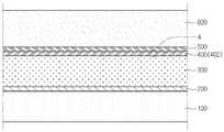
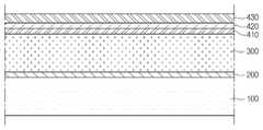
도 1은 제1 실시예에 따른 태양전지의 일 단면을 도시한 단면도이다.
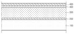
도 2는 도 1의 A를 확대하여 도시한 확대도이다.
도 3은 제2 실시예에 따른 태양전지에 포함되는 버퍼층의 단면도이다.
도 4는 제2 실시예에 따른 태양전지의 각 층에 포함되는 나트륨 농도를 도시한 그래프이다.
도 5 내지 도 7은 제1 실시예에 따른 태양전지를 제조하기 위한 공정을 도시한 단면도들이다.
도 8 내지 도 10은 제2 실시예에 따른 태양전지를 제조하기 위한 공정을 도시한 단면도들이다.1 is a cross-sectional view showing a cross section of a solar cell according to a first embodiment.
FIG. 2 is an enlarged view of an enlarged view of portion A of FIG. 1.
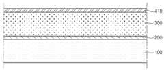
3 is a cross-sectional view of the buffer layer included in the solar cell according to the second embodiment.
4 is a graph illustrating sodium concentration included in each layer of the solar cell according to the second embodiment.
5 to 7 are cross-sectional views illustrating a process for manufacturing the solar cell according to the first embodiment.
8 to 10 are cross-sectional views illustrating a process for manufacturing a solar cell according to the second embodiment.
실시예들의 설명에 있어서, 각 층(막), 영역, 패턴 또는 구조물들이 기판, 각 층(막), 영역, 패드 또는 패턴들의 “상/위(on)”에 또는 “하/아래(under)”에 형성된다는 기재는, 직접(directly) 또는 다른 층을 개재하여 형성되는 것을 모두 포함한다. 각 층의 상/위 또는 하/아래에 대한 기준은 도면을 기준으로 설명한다.In the description of embodiments, each layer, region, pattern, or structure may be “on” or “under” the substrate, each layer, region, pad, or pattern. Substrate formed in ”includes all formed directly or through another layer. Criteria for the top / bottom or bottom / bottom of each layer will be described with reference to the drawings.
도면에서 각 층(막), 영역, 패턴 또는 구조물들의 두께나 크기는 설명의 명확성 및 편의를 위하여 변형될 수 있으므로, 실제 크기를 전적으로 반영하는 것은 아니다.The thickness or the size of each layer (film), region, pattern or structure in the drawings may be modified for clarity and convenience of explanation, and thus does not entirely reflect the actual size.
이하, 첨부한 도면을 참조하여 본 발명의 실시예를 상세하게 설명하면 다음과 같다.Hereinafter, embodiments of the present invention will be described in detail with reference to the accompanying drawings.
먼저 도 1 및 도 2를 참조하여, 제1 실시예에 따른 태양전지를 상세하게 설명한다. 도 1은 제1 실시예에 따른 태양전지의 일 단면을 도시한 단면도이다. 도 2는 도 1의 A를 확대하여 도시한 확대도이다.First, the solar cell according to the first embodiment will be described in detail with reference to FIGS. 1 and 2. 1 is a cross-sectional view showing a cross section of a solar cell according to a first embodiment. FIG. 2 is an enlarged view of an enlarged view of portion A of FIG. 1.
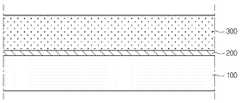
도 1을 참조하면, 태양전지는 지지기판(100), 후면전극층(200), 광 흡수층(300), 버퍼층(400), 고저항 버퍼층(500) 및 전면전극층(600)을 포함한다.Referring to FIG. 1, the solar cell includes a
상기 지지기판(100)은 플레이트 형상을 가지며, 상기 후면전극층(200), 상기 광 흡수층(300), 버퍼층(400), 고저항 버퍼층(500) 및 상기 전면전극층(600)을 지지한다.The supporting
상기 지지기판(100)은 절연체일 수 있다. 상기 지지기판(100)은 유리기판, 플라스틱기판 또는 금속기판일 수 있다. 더 자세하게, 상기 지지기판(100)은 소다 라임 글래스(soda lime glass) 기판일 수 있다. 상기 지지기판(100)은 투명할 수 있다. 상기 지지기판(100)은 리지드하거나 플렉서블할 수 있다.The
상기 후면전극층(200)은 상기 지지기판(100)의 상면에 배치된다. 상기 후면전극층(200)은 도전층이다. 상기 후면전극층(200)으로 사용되는 물질의 예로서는 몰리브덴(Mo) 등의 금속을 들 수 있다.The
또한, 상기 후면전극층(200)은 두 개 이상의 층들을 포함할 수 있다. 이때, 각각의 층들은 같은 금속으로 형성되거나, 서로 다른 금속으로 형성될 수 있다.In addition, the
상기 광 흡수층(300)은 상기 후면전극층(200) 상에 배치된다. 상기 광 흡수층(300)은 Ⅰ-Ⅲ-Ⅵ족계 화합물을 포함한다. 예를 들어, 상기 광 흡수층(300)은 구리-인듐-갈륨-셀레나이드계(Cu(In,Ga)Se2;CIGS계) 결정 구조, 구리-인듐-셀레나이드계 또는 구리-갈륨-셀레나이드계 결정 구조를 가질 수 있다.The light
상기 광 흡수층(300)의 에너지 밴드갭(band gap)은 약 1eV 내지 1.8eV일 수 있다.The energy band gap of the
상기 버퍼층(400)은 상기 광 흡수층(300) 상에 배치된다. 상기 버퍼층(400)은 상기 광 흡수층(300)에 직접 접촉한다.The
상기 버퍼층(400)은 두 개 이상의 층을 포함할 수 있다. 구체적으로, 도 2를 참조하면, 상기 버퍼층(400)은 제2 버퍼층(420) 및 제3 버퍼층(430)을 포함할 수 있다.The
상기 제2 버퍼층(420)은 상기 광 흡수층(300) 상에 위치한다.The
상기 제2 버퍼층(420)은 셀레늄(Se)을 포함한다. 구체적으로, 상기 제2 버퍼층(420)은 카드뮴셀레나이드(CdSe)를 포함한다.The
상기 제2 버퍼층(420)의 두께는 10 nm 내지 20 nm 일 수 있다.The thickness of the
상기 제2 버퍼층(420)의 에너지 밴드갭(band gap)은 약 1.7 eV 일 수 있다.The energy band gap of the
상기 제3 버퍼층(430)은 상기 제2 버퍼층(420) 상에 위치한다.The
상기 제3 버퍼층(430)은 황화물을 포함한다. 구체적으로, 상기 제3 버퍼층(430)은 황화카드뮴(CdS)을 포함한다.The
상기 제3 버퍼층(430)의 두께는 30 nm 내지 40 nm 일 수 있다.The thickness of the
상기 제3 버퍼층(430)의 에너지 밴드갭은 약 2.4 eV 일 수 있다.The energy band gap of the
상기 버퍼층(400)의 에너지 밴드갭은 계단 형상, 즉, 순차적으로 증가한다. 즉, 상기 버퍼층(400)은 제2 버퍼층(420) 및 제3 버퍼층(430)으로 구분되기 때문에, 순차적인 에너지 밴드갭을 가진다.The energy band gap of the
즉, 상기 광 흡수층(300)과 상기 버퍼층(400)사이의 에너지 밴드갭 차이를 줄여 광기전력 수득을 용이하게 할 수 있다.That is, the energy band gap difference between the light absorbing
따라서, 상기 버퍼층(400)을 통하여, 전자가 용이하게 수송될 수 있고, 실시예에 따른 태양전지는 향상된 효율을 가진다.Therefore, electrons can be easily transported through the
즉, 황화 카드뮴만으로 이루어진 버퍼층(400)을 가지는 기존 태양전지와 비교하여, 실시예에 따른 태양전지는 향상된 효율을 가진다.That is, compared with the conventional solar cell having a
상기 고저항 버퍼층(500)은 상기 버퍼층(400) 상에 배치된다. 상기 고저항 버퍼층(500)은 불순물이 도핑되지 않은 징크 옥사이드(i-ZnO)를 포함한다. 상기 고저항 버퍼층(500)의 에너지 밴드갭은 약 3.1eV 내지 3.3eV일 수 있다.The high
상기 전면전극층(600)은 상기 광 흡수층(300) 상에 배치된다. 더 자세하게, 상기 전면전극층(600)은 상기 고저항 버퍼층(500) 상에 배치된다.The
상기 전면전극층(600)은 상기 고저항 버퍼층(500) 상에 배치된다. 상기 전면전극층(600)은 투명하다. 상기 전면전극층(600)으로 사용되는 물질의 예로서는 알루미늄이 도핑된 징크 옥사이드(Al doped ZnO;AZO), 인듐 징크 옥사이드(indium zinc oxide;IZO) 또는 인듐 틴 옥사이드(indium tin oxide;ITO) 등을 들 수 있다.The
상기 전면전극층(600)의 두께는 약 500㎚ 내지 약 1.5㎛일 수 있다. 또한, 상기 전면전극층(600)이 알루미늄이 도핑되는 징크 옥사이드로 형성되는 경우, 알루미늄은 약 2.5wt% 내지 약 3.5wt%의 비율로 도핑될 수 있다. 상기 전면전극층(600)은 도전층이다.The
이하, 도 3 및 도 4를 참조하여, 제2 실시예에 따른 태양전지를 설명한다. 명확하고 간략한 설명을 위하여 제1 실시예와 동일 또는 유사한 부분에 대해서는 상세한 설명을 생략한다.Hereinafter, a solar cell according to a second embodiment will be described with reference to FIGS. 3 and 4. Detailed descriptions of parts identical or similar to those of the first embodiment will be omitted for clarity and simplicity.
도 3은 제2 실시예에 따른 태양전지에 포함되는 버퍼층(400)의 단면도이다. 도 4는 제2 실시예에 따른 태양전지의 각 층에 포함되는 나트륨 농도를 도시한 그래프이다.3 is a cross-sectional view of the
도 3을 참조하면, 제2 실시예에 따른 태양전지에 포함되는 버퍼층(400)은 제1 버퍼층(410), 제2 버퍼층(420) 및 제3 버퍼층(430)을 포함한다.Referring to FIG. 3, the
상기 제1 버퍼층(410)은 상기 광 흡수층(300) 상에 위치한다.The
상기 제1 버퍼층(410)은 1족 및 6족계 화합물을 포함한다. 상기 제1 버퍼층(410)은 나트륨(Na)을 포함할 수 있다. 구체적으로, 상기 제1 버퍼층(410)은 셀렌화나트륨(Na2Se)를 포함할 수 있다.The
상기 제1 버퍼층(410)의 두께는 10 nm 이하일 수 있다.The thickness of the
상기 제2 버퍼층(420)은 상기 제1 버퍼층(410) 상에 위치한다.The
상기 제2 버퍼층(420) 및 상기 제3 버퍼층(430)은 제1 실시예에 포함되는 제2 버퍼층(420) 및 제3 버퍼층(430)과 동일 또는 유사하므로 상세한 설명을 생략한다.Since the
상기 제1 버퍼층(410)이 상기 광 흡수층(300) 및 상기 제2 버퍼층(420) 사이에 삽입됨으로써, 상기 광 흡수층(300) 및 상기 제2 버퍼층(420)과의 결합구조를 높일 수 있다.The
또한, 상기 제1 버퍼층(410)이 삽입됨으로써, 상기 광 흡수층(300)의 구리 베이컨시(Cu vacancy)에 나트륨이 도핑될 수 있다. 도 4를 참조하면, 상기 광 흡수층(300)의 나트륨(Na) 농도는 상기 제1 버퍼층(410)에 가까워질수록 증가한다. 즉, 상기 광 흡수층(300)의 상기 제1 버퍼층(410)과 가깝게 위치한 면에서 나트륨이 많이 분포함으로써, 상기 광 흡수층(300)과 상기 버퍼층(400)이 유사한 에너지 밴드갭을 가질 수 있다. 이를 통해, 전자의 수득율을 높일 수 있다.In addition, sodium may be doped into the copper vacancy of the
이하, 도 5 내지 도 7을 참조하여, 제1 실시예에 따른 태양전지의 제조 방법을 설명한다. 도 5 내지 도 7은 제1 실시예에 따른 태양전지를 제조하기 위한 공정을 도시한 단면도들이다.Hereinafter, a method of manufacturing the solar cell according to the first embodiment will be described with reference to FIGS. 5 to 7. 5 to 7 are cross-sectional views illustrating a process for manufacturing the solar cell according to the first embodiment.
제1 실시예에 따른 태양전지의 제조 방법은, 지지기판(100) 상에 후면전극층(200)을 형성하는 단계, 광 흡수층(300)을 형성하는 단계, 제2 버퍼층(420)을 형성하는 단계 및 제3 버퍼층(430)을 형성하는 단계를 포함한다.In the method of manufacturing a solar cell according to the first embodiment, forming the
도 5를 참조하면, 지지기판(100) 상에 스퍼터링 공정에 의해서 몰리브덴 등과 같은 금속이 증착되고, 후면전극층(200)이 형성된다. 상기 후면전극층(200)은 공정 조건이 서로 다른 두 번의 공정들에 의해서 형성될 수 있다.Referring to FIG. 5, a metal such as molybdenum is deposited on the
상기 지지기판(100) 및 상기 후면전극층(200) 사이에는 확산 방지막과 같은 추가적인 층이 개재될 수 있다.An additional layer such as a diffusion barrier may be interposed between the
이어서, 상기 후면전극층(200) 상에 광 흡수층(300)이 형성된다. 상기 광 흡수층(300)은 스퍼터링 공정 또는 증발법 등에 의해서 형성될 수 있다.Subsequently, the
예를 들어, 상기 광 흡수층(300)을 형성하기 위해서 구리, 인듐, 갈륨, 셀레늄을 동시 또는 구분하여 증발시키면서 구리-인듐-갈륨-셀레나이드계(Cu(In,Ga)Se2;CIGS계)의 광 흡수층(300)을 형성하는 방법과 금속 프리커서 막을 형성시킨 후 셀레니제이션(Selenization) 공정에 의해 형성시키는 방법이 폭넓게 사용되고 있다.For example, a copper-indium-gallium-selenide-based (Cu (In, Ga) Se 2; CIGS-based) light-emitting layer is formed while simultaneously evaporating copper, indium, gallium, A method of forming the
금속 프리커서 막을 형성시킨 후 셀레니제이션 하는 것을 세분화하면, 구리 타겟, 인듐 타겟, 갈륨 타겟을 사용하는 스퍼터링 공정에 의해서, 상기 이면전극(200) 상에 금속 프리커서 막이 형성된다.After the metal precursor film is formed and then subjected to selenization, a metal precursor film is formed on the
이후, 상기 금속 프리커서 막은 셀레이제이션(selenization) 공정에 의해서, 구리-인듐-갈륨-셀레나이드계(Cu(In,Ga)Se2;CIGS계)의 광 흡수층(300)이 형성된다.Subsequently, the metal precursor film is formed of a copper-indium-gallium-selenide (Cu (In, Ga) Se 2; CIGS-based) light absorbing
이와는 다르게, 상기 구리 타겟, 인듐 타겟, 갈륨 타겟을 사용하는 스퍼터링 공정 및 상기 셀레니제이션 공정은 동시에 진행될 수 있다.Alternatively, the copper target, the indium target, the sputtering process using the gallium target, and the selenization process may be performed simultaneously.
이와는 다르게, 구리 타겟 및 인듐 타겟 만을 사용하거나, 구리 타겟 및 갈륨 타겟을 사용하는 스퍼터링 공정 및 셀레니제이션 공정에 의해서, CIS계 또는 CIG계 광 흡수층(300)이 형성될 수 있다.Alternatively, the CIS-based or CIG-based
이후, 도 6을 참조하면, 상기 광 흡수층(300) 상에 제2 버퍼층(420)이 형성된다.Thereafter, referring to FIG. 6, a
상기 제2 버퍼층(420)은 화학 용액 증착 공정(chemical bath depositon;CBD), 화학 기상 증착(chemical vapor deposition;CVD) 공정, 스프레이법 또는 물리 기상 증착(physical vapor deposition;PVD) 공정에 의해서 형성될 수 있다.The
일례로, 상기 제2 버퍼층(420)은 Cd(EtBu-dsc)2 전구체를 이용한 화학 기상 증착 공정을 통해 형성될 수 있다.For example, the
이후, 도 7을 참조하면, 상기 제2 버퍼층(420) 상에 제3 버퍼층(430)이 형성된다.Subsequently, referring to FIG. 7, a
상기 제3 버퍼층(430)은 CBD, CVD 공정, 스프레이법 또는 PVD 공정에 의해서 형성될 수 있다.The
일례로, 상기 제3 버퍼층(430)은 화학 용액 증착 공정(CBD)에 의해서 형성될 수 있다. 예를 들어, 상기 제2 버퍼층(420)이 형성된 후, 상기 제2 버퍼층(420)은 황화 카드뮴을 형성하기 위한 물질들을 포함하는 용액에 침지되고, 상기 제2 버퍼층(420) 상에 황화 카드뮴을 포함하는 상기 제3 버퍼층(430)이 형성된다.For example, the
이후, 상기 제3 버퍼층(430) 상에 징크 옥사이드가 스퍼터링 공정 등에 의해서 증착되고, 고저항 버퍼층이 형성된다.Thereafter, zinc oxide is deposited on the
상기 고저항 버퍼층 상에 전면전극층이 형성된다. 상기 전면전극층을 형성하기 위해서, 상기 고저항 버퍼층 상에 투명한 도전물질이 적층된다. 상기 투명한 도전물질의 예로서는 알루미늄 도핑된 징크 옥사이드 등을 들 수 있다.The front electrode layer is formed on the high resistance buffer layer. In order to form the front electrode layer, a transparent conductive material is stacked on the high resistance buffer layer. Examples of the transparent conductive material include aluminum doped zinc oxide and the like.
이하, 도 8 내지 도 10을 참조하여, 제2 실시예에 따른 태양전지의 제조 방법을 설명한다.Hereinafter, a method of manufacturing a solar cell according to a second embodiment will be described with reference to FIGS. 8 to 10.
도 8 내지 도 10은 제2 실시예에 따른 태양전지를 제조하기 위한 공정을 도시한 단면도들이다.8 to 10 are cross-sectional views illustrating a process for manufacturing a solar cell according to the second embodiment.
도 8을 참조하면, 상기 광 흡수층(300) 상에 제1 버퍼층(410)이 형성된다.Referring to FIG. 8, a
상기 제1 버퍼층(410)은 CBD, CVD 공정, 스프레이법 또는 PVD 공정에 의해서 형성될 수 있다.The
이후, 도 9 및 도 10을 참조하면, 상기 제1 버퍼층(410) 상에 제2 버퍼층(420) 및 제3 버퍼층(430)이 형성될 수 있다.9 and 10, a
상술한 실시예에 설명된 특징, 구조, 효과 등은 본 발명의 적어도 하나의 실시예에 포함되며, 반드시 하나의 실시예에만 한정되는 것은 아니다. 나아가, 각 실시예에서 예시된 특징, 구조, 효과 등은 실시예들이 속하는 분야의 통상의 지식을 가지는 자에 의하여 다른 실시예들에 대해서도 조합 또는 변형되어 실시 가능하다. 따라서 이러한 조합과 변형에 관계된 내용들은 본 발명의 범위에 포함되는 것으로 해석되어야 할 것이다.The features, structures, effects and the like described in the foregoing embodiments are included in at least one embodiment of the present invention and are not necessarily limited to one embodiment. In addition, the features, structures, effects, and the like illustrated in the embodiments may be combined or modified with respect to other embodiments by those skilled in the art to which the embodiments belong. Therefore, it should be understood that the present invention is not limited to these combinations and modifications.
또한, 이상에서 실시예들을 중심으로 설명하였으나 이는 단지 예시일 뿐 본 발명을 한정하는 것이 아니며, 본 발명이 속하는 분야의 통상의 지식을 가진 자라면 본 실시예의 본질적인 특성을 벗어나지 않는 범위에서 이상에 예시되지 않은 여러 가지의 변형과 응용이 가능함을 알 수 있을 것이다. 예를 들어, 실시예들에 구체적으로 나타난 각 구성 요소는 변형하여 실시할 수 있는 것이다. 그리고 이러한 변형과 응용에 관계된 차이점들은 첨부한 청구 범위에서 규정하는 본 발명의 범위에 포함되는 것으로 해석되어야 할 것이다.While the present invention has been particularly shown and described with reference to exemplary embodiments thereof, it is clearly understood that the same is by way of illustration and example only and is not to be construed as limiting the scope of the present invention. It can be seen that various modifications and applications are possible. For example, each component specifically shown in the embodiments may be modified. It is to be understood that the present invention may be embodied in many other specific forms without departing from the spirit or essential characteristics thereof.
Claims (10)
Translated fromKorean상기 후면전극층 상에 배치되는 광 흡수층; 및
상기 광 흡수층 상에 배치되는 버퍼층을 포함하고,
상기 버퍼층은 제1 버퍼층, 상기 제1 버퍼층 상에 위치하는 제2 버퍼층 및 상기 제2 버퍼층 상에 위치하는 제3 버퍼층을 포함하며,
상기 제1 버퍼층은 1족 및 6족계 화합물을 포함하는 태양전지.A rear electrode layer;
A light absorbing layer disposed on the back electrode layer; And
And a buffer layer disposed on the light absorbing layer,
The buffer layer includes a first buffer layer, a second buffer layer positioned on the first buffer layer, and a third buffer layer positioned on the second buffer layer,
The first buffer layer is a solar cell comprising a group 1 and 6-based compound.
상기 제1 버퍼층은 셀렌화나트륨(Na2Se)를 포함하는 태양전지.The method of claim 1,
The first buffer layer is a solar cell containing sodium selenide (Na 2 Se).
상기 제2 버퍼층은 카드뮴셀레나이드(CdSe)를 포함하는 태양전지.The method of claim 1,
The second buffer layer includes a cadmium selenide (CdSe).
상기 제3 버퍼층은 황화카드뮴(CdS)을 포함하는 태양전지.The method of claim 1,
The third buffer layer is a solar cell containing cadmium sulfide (CdS).
상기 광 흡수층은 상기 제1 버퍼층에 가까워질수록 나트륨(Na) 농도가 증가하는 태양전지.The method of claim 1,
The light absorbing layer is a solar cell increases the concentration of sodium (Na) closer to the first buffer layer.
상기 제1 버퍼층의 두께는 10 nm 이하인 태양전지.The method of claim 1,
The first buffer layer has a thickness of 10 nm or less.
상기 제2 버퍼층의 두께는 10 nm 내지 20 nm 인 태양전지.The method of claim 1,
The second buffer layer has a thickness of 10 nm to 20 nm solar cell.
상기 제3 버퍼층의 두께는 30 nm 내지 40 nm 인 태양전지.The method of claim 1,
The third buffer layer has a thickness of 30 nm to 40 nm.
상기 후면 전극층 상에 광 흡수층을 형성하는 단계;
상기 광 흡수층 상에 셀레늄을 포함하는 제2 버퍼층을 형성하는 단계; 및
상기 제2 버퍼층 상에 황화물을 포함하는 제3 버퍼층을 형성하는 단계를 포함하는 태양전지 제조 방법.Forming a back electrode layer on the substrate;
Forming a light absorbing layer on the back electrode layer;
Forming a second buffer layer including selenium on the light absorbing layer; And
Forming a third buffer layer including a sulfide on the second buffer layer solar cell manufacturing method.
상기 광 흡수층을 형성하는 단계 및 상기 제2 버퍼층을 형성하는 단계 사이에 상기 광 흡수층 상에 1족 및 6족계 화합물을 포함하는 제1 버퍼층을 형성하는 단계를 포함하는 태양전지 제조 방법.10. The method of claim 9,
And forming a first buffer layer including Group 1 and Group 6 compounds on the light absorbing layer between the forming of the light absorbing layer and the forming of the second buffer layer.
Priority Applications (4)
| Application Number | Priority Date | Filing Date | Title |
|---|---|---|---|
| KR1020110106121AKR101210046B1 (en) | 2011-10-17 | 2011-10-17 | Solar cell and method of fabricating the same |
| PCT/KR2012/008444WO2013058521A1 (en) | 2011-10-17 | 2012-10-16 | Solar cell and method of fabricating the same |
| CN201280062499.8ACN103999236B (en) | 2011-10-17 | 2012-10-16 | Solar cell and manufacturing method thereof |
| US14/352,385US9640685B2 (en) | 2011-10-17 | 2012-10-16 | Solar cell and method of fabricating the same |
Applications Claiming Priority (1)
| Application Number | Priority Date | Filing Date | Title |
|---|---|---|---|
| KR1020110106121AKR101210046B1 (en) | 2011-10-17 | 2011-10-17 | Solar cell and method of fabricating the same |
Publications (1)
| Publication Number | Publication Date |
|---|---|
| KR101210046B1true KR101210046B1 (en) | 2012-12-07 |
Family
ID=47907229
Family Applications (1)
| Application Number | Title | Priority Date | Filing Date |
|---|---|---|---|
| KR1020110106121AExpired - Fee RelatedKR101210046B1 (en) | 2011-10-17 | 2011-10-17 | Solar cell and method of fabricating the same |
Country Status (4)
| Country | Link |
|---|---|
| US (1) | US9640685B2 (en) |
| KR (1) | KR101210046B1 (en) |
| CN (1) | CN103999236B (en) |
| WO (1) | WO2013058521A1 (en) |
Cited By (1)
| Publication number | Priority date | Publication date | Assignee | Title |
|---|---|---|---|---|
| WO2021107221A1 (en)* | 2019-11-28 | 2021-06-03 | 한국과학기술연구원 | Cis-based thin film, solar cell comprising same, and production method therefor |
Families Citing this family (3)
| Publication number | Priority date | Publication date | Assignee | Title |
|---|---|---|---|---|
| JP6738078B2 (en)* | 2017-02-27 | 2020-08-12 | 国立研究開発法人産業技術総合研究所 | Solar cell and manufacturing method thereof |
| CN108321216A (en)* | 2018-01-30 | 2018-07-24 | 北京铂阳顶荣光伏科技有限公司 | A kind of oxygen zinc-magnesium material, preparation method and the solar cell of adjustable optical band gap |
| CN110061087B (en)* | 2019-04-26 | 2020-02-21 | 圣晖莱南京能源科技有限公司 | A kind of solar cell and its buffer layer and preparation method |
Citations (2)
| Publication number | Priority date | Publication date | Assignee | Title |
|---|---|---|---|---|
| JP2002373995A (en) | 2001-06-15 | 2002-12-26 | Honda Motor Co Ltd | Solar cell manufacturing method |
| WO2009110093A1 (en) | 2008-03-07 | 2009-09-11 | 昭和シェル石油株式会社 | Integrated structure of cis-type solar battery |
Family Cites Families (14)
| Publication number | Priority date | Publication date | Assignee | Title |
|---|---|---|---|---|
| US5501744A (en)* | 1992-01-13 | 1996-03-26 | Photon Energy, Inc. | Photovoltaic cell having a p-type polycrystalline layer with large crystals |
| US5261968A (en)* | 1992-01-13 | 1993-11-16 | Photon Energy, Inc. | Photovoltaic cell and method |
| JP3527815B2 (en)* | 1996-11-08 | 2004-05-17 | 昭和シェル石油株式会社 | Method for producing transparent conductive film of thin film solar cell |
| JP2007123720A (en)* | 2005-10-31 | 2007-05-17 | Rohm Co Ltd | Photoelectric conversion device and manufacturing method thereof |
| EP1964180B1 (en)* | 2005-12-21 | 2010-08-04 | Saint-Gobain Glass France S.A. | Process of making a thin-film photovoltaic device |
| US20080023059A1 (en)* | 2006-07-25 | 2008-01-31 | Basol Bulent M | Tandem solar cell structures and methods of manufacturing same |
| WO2009012345A2 (en)* | 2007-07-16 | 2009-01-22 | Ascent Solar Technologies, Inc. | Hybrid multi-junction photovoltaic cells and associated methods |
| JP4974986B2 (en) | 2007-09-28 | 2012-07-11 | 富士フイルム株式会社 | Solar cell substrate and solar cell |
| US8779283B2 (en)* | 2007-11-29 | 2014-07-15 | General Electric Company | Absorber layer for thin film photovoltaics and a solar cell made therefrom |
| FR2939240B1 (en)* | 2008-12-03 | 2011-02-18 | Saint Gobain | LAYERED ELEMENT AND PHOTOVOLTAIC DEVICE COMPRISING SUCH A MEMBER |
| KR101231364B1 (en) | 2009-10-01 | 2013-02-07 | 엘지이노텍 주식회사 | Solar cell and method of fabircating the same |
| KR101034150B1 (en) | 2009-11-02 | 2011-05-13 | 엘지이노텍 주식회사 | Solar cell and manufacturing method thereof |
| CN102484164B (en) | 2010-03-05 | 2015-04-29 | 株式会社东芝 | Compound thin film solar cell and manufacturing method thereof |
| US8551802B2 (en)* | 2011-09-12 | 2013-10-08 | Intermolecular, Inc. | Laser annealing for thin film solar cells |
- 2011
- 2011-10-17KRKR1020110106121Apatent/KR101210046B1/ennot_activeExpired - Fee Related
- 2012
- 2012-10-16USUS14/352,385patent/US9640685B2/ennot_activeExpired - Fee Related
- 2012-10-16WOPCT/KR2012/008444patent/WO2013058521A1/enactiveApplication Filing
- 2012-10-16CNCN201280062499.8Apatent/CN103999236B/ennot_activeExpired - Fee Related
Patent Citations (2)
| Publication number | Priority date | Publication date | Assignee | Title |
|---|---|---|---|---|
| JP2002373995A (en) | 2001-06-15 | 2002-12-26 | Honda Motor Co Ltd | Solar cell manufacturing method |
| WO2009110093A1 (en) | 2008-03-07 | 2009-09-11 | 昭和シェル石油株式会社 | Integrated structure of cis-type solar battery |
Cited By (1)
| Publication number | Priority date | Publication date | Assignee | Title |
|---|---|---|---|---|
| WO2021107221A1 (en)* | 2019-11-28 | 2021-06-03 | 한국과학기술연구원 | Cis-based thin film, solar cell comprising same, and production method therefor |
Also Published As
| Publication number | Publication date |
|---|---|
| CN103999236A (en) | 2014-08-20 |
| US20140238486A1 (en) | 2014-08-28 |
| WO2013058521A1 (en) | 2013-04-25 |
| CN103999236B (en) | 2016-08-24 |
| US9640685B2 (en) | 2017-05-02 |
Similar Documents
| Publication | Publication Date | Title |
|---|---|---|
| KR101219948B1 (en) | Solar cell apparatus and method of fabricating the same | |
| KR101283113B1 (en) | Solar cell module and manufacturing method thereof | |
| US9379266B2 (en) | Solar cell module and method of fabricating the same | |
| KR101210046B1 (en) | Solar cell and method of fabricating the same | |
| KR101210110B1 (en) | Solar cell and method of fabricating the same | |
| KR101405639B1 (en) | Solar cell and method of fabricating the same | |
| KR101173419B1 (en) | Solar cell and method of fabricating the same | |
| KR20150039535A (en) | Solar cell and method of fabricating the same | |
| KR101210034B1 (en) | Solar cell and method of fabricating the same | |
| KR101306525B1 (en) | Solar cell module and method of fabricating the same | |
| KR101382819B1 (en) | Photovoltaic apparatus and method of fabricating the same | |
| KR101393743B1 (en) | Solar cell and method of fabricating the same | |
| KR20130070461A (en) | Solar cell and method of fabricating the same | |
| KR101349596B1 (en) | Solar cell and method of fabricating the same | |
| US20150136223A1 (en) | Solar cell and method for manufacturing the same | |
| KR101349432B1 (en) | Photovoltaic apparatus and method of fabricating the same | |
| KR101306436B1 (en) | Solar cell apparatus and method of fabricating the same | |
| KR20150031978A (en) | Solar cell | |
| KR101326885B1 (en) | Solar cell and method of fabricating the same | |
| KR20140003802A (en) | Solar cell and method of fabricating the same | |
| KR101273123B1 (en) | Solar cell apparatus and method of fabricating the same | |
| KR20140047258A (en) | Solar cell and method of fabricating the same | |
| KR101417321B1 (en) | Solar cell and method of fabricating the same | |
| KR101231398B1 (en) | Solar cell apparatus and method of fabricating the same | |
| KR101144475B1 (en) | Solar cell apparatus and method of fabricating the same |
Legal Events
| Date | Code | Title | Description |
|---|---|---|---|
| A201 | Request for examination | ||
| PA0109 | Patent application | St.27 status event code:A-0-1-A10-A12-nap-PA0109 | |
| PA0201 | Request for examination | St.27 status event code:A-1-2-D10-D11-exm-PA0201 | |
| D13-X000 | Search requested | St.27 status event code:A-1-2-D10-D13-srh-X000 | |
| D14-X000 | Search report completed | St.27 status event code:A-1-2-D10-D14-srh-X000 | |
| E701 | Decision to grant or registration of patent right | ||
| PE0701 | Decision of registration | St.27 status event code:A-1-2-D10-D22-exm-PE0701 | |
| GRNT | Written decision to grant | ||
| PR0701 | Registration of establishment | St.27 status event code:A-2-4-F10-F11-exm-PR0701 | |
| PR1002 | Payment of registration fee | St.27 status event code:A-2-2-U10-U11-oth-PR1002 Fee payment year number:1 | |
| PG1601 | Publication of registration | St.27 status event code:A-4-4-Q10-Q13-nap-PG1601 | |
| P22-X000 | Classification modified | St.27 status event code:A-4-4-P10-P22-nap-X000 | |
| PN2301 | Change of applicant | St.27 status event code:A-5-5-R10-R13-asn-PN2301 St.27 status event code:A-5-5-R10-R11-asn-PN2301 | |
| FPAY | Annual fee payment | Payment date:20151105 Year of fee payment:4 | |
| PR1001 | Payment of annual fee | St.27 status event code:A-4-4-U10-U11-oth-PR1001 Fee payment year number:4 | |
| FPAY | Annual fee payment | Payment date:20161104 Year of fee payment:5 | |
| PR1001 | Payment of annual fee | St.27 status event code:A-4-4-U10-U11-oth-PR1001 Fee payment year number:5 | |
| R18-X000 | Changes to party contact information recorded | St.27 status event code:A-5-5-R10-R18-oth-X000 | |
| FPAY | Annual fee payment | Payment date:20171107 Year of fee payment:6 | |
| PR1001 | Payment of annual fee | St.27 status event code:A-4-4-U10-U11-oth-PR1001 Fee payment year number:6 | |
| R18-X000 | Changes to party contact information recorded | St.27 status event code:A-5-5-R10-R18-oth-X000 | |
| LAPS | Lapse due to unpaid annual fee | ||
| PC1903 | Unpaid annual fee | St.27 status event code:A-4-4-U10-U13-oth-PC1903 Not in force date:20181204 Payment event data comment text:Termination Category : DEFAULT_OF_REGISTRATION_FEE | |
| PC1903 | Unpaid annual fee | St.27 status event code:N-4-6-H10-H13-oth-PC1903 Ip right cessation event data comment text:Termination Category : DEFAULT_OF_REGISTRATION_FEE Not in force date:20181204 | |
| R18-X000 | Changes to party contact information recorded | St.27 status event code:A-5-5-R10-R18-oth-X000 | |
| PN2301 | Change of applicant | St.27 status event code:A-5-5-R10-R13-asn-PN2301 St.27 status event code:A-5-5-R10-R11-asn-PN2301 | |
| P22-X000 | Classification modified | St.27 status event code:A-4-4-P10-P22-nap-X000 |