KR101209651B1 - Apparatus to Sputter - Google Patents
Apparatus to SputterDownload PDFInfo
- Publication number
- KR101209651B1 KR101209651B1KR1020100023465AKR20100023465AKR101209651B1KR 101209651 B1KR101209651 B1KR 101209651B1KR 1020100023465 AKR1020100023465 AKR 1020100023465AKR 20100023465 AKR20100023465 AKR 20100023465AKR 101209651 B1KR101209651 B1KR 101209651B1
- Authority
- KR
- South Korea
- Prior art keywords
- target
- magnets
- pole plate
- substrate
- magnet
- Prior art date
- Legal status (The legal status is an assumption and is not a legal conclusion. Google has not performed a legal analysis and makes no representation as to the accuracy of the status listed.)
- Expired - Fee Related
Links
Images


Landscapes
- Chemical & Material Sciences (AREA)
- Engineering & Computer Science (AREA)
- Chemical Kinetics & Catalysis (AREA)
- Materials Engineering (AREA)
- Mechanical Engineering (AREA)
- Metallurgy (AREA)
- Organic Chemistry (AREA)
- Physical Vapour Deposition (AREA)
- Physics & Mathematics (AREA)
- Plasma & Fusion (AREA)
- Analytical Chemistry (AREA)
Abstract
Translated fromKoreanDescription
Translated fromKorean본 발명은, 스퍼터 장치에 관한 것으로서, 보다 상세하게는, 타겟에 대한 마그네트의 위치를 손쉽게 조정하면서 세팅할 수 있어 종래기술 대비 마그네트의 세팅 작업에 따른 실패 비용 및 시간 손실을 현저하게 감소시킬 수 있는 스퍼터 장치에 관한 것이다.The present invention relates to a sputtering device, and more particularly, it can be set while easily adjusting the position of the magnet relative to the target, which can significantly reduce the failure cost and time loss due to the setting operation of the magnet compared to the prior art It relates to a sputter apparatus.
LCD(Liquid Crystal Display), PDP(Plasma Display Panel) 및 OLED(Organic Light Emitting Diodes) 등의 평판디스플레이나 반도체는 박막 증착(Deposition), 식각(Etching) 등의 다양한 공정을 거쳐 제품으로 출시된다.Flat panel displays and semiconductors, such as liquid crystal displays (LCDs), plasma display panels (PDPs), and organic light emitting diodes (OLEDs), are released as products through various processes such as thin film deposition and etching.
다양한 공정 중에서 특히 박막 증착 공정은, 증착의 중요한 원칙에 따라 크게 두 가지로 나뉜다.Among the various processes, in particular, the thin film deposition process is largely divided into two according to the important principles of deposition.
하나는 화학적 기상 증착(Chemical Vapor deposition, CVD)이고, 다른 하나는 물리적 기상 증착(Physical Vapor Deposition, PVD)이며, 이들은 현재 공정의 특성에 맞게 널리 사용되고 있다.One is Chemical Vapor Deposition (CVD) and the other is Physical Vapor Deposition (PVD), which is now widely used to suit the nature of the process.
화학적 기상 증착은, 외부의 고주파 전원에 의해 플라즈마(Plasma)화 되어 높은 에너지를 갖는 실리콘계 화합물 이온(ion)이 전극을 통해 샤워헤드로부터 분출되어 기판 상에 증착되도록 하는 방식이다.Chemical vapor deposition is a method in which plasma is formed by an external high frequency power source so that silicon-based compound ions having high energy are ejected from a showerhead through an electrode and deposited on a substrate.
이에 반해, 스퍼터 장치로 대변될 수 있는 물리적 기상 증착은, 플라즈마 내의 이온에 충분한 에너지를 걸어주어 타겟에 충돌되도록 한 후에 타겟으로부터 튀어나오는, 즉 스퍼터되는 타겟 원자가 기판 상에 증착되도록 하는 방식이다.In contrast, physical vapor deposition, which can be represented by a sputter device, is a method in which sufficient energy is applied to the ions in the plasma to impinge on the target and then ejected from the target, i.e., sputtered target atoms are deposited on the substrate.
물론, 물리적 기상 증착에는 전술한 스퍼터(Sputter) 방식 외에도 이-빔(E-Beam), 이베퍼레이션(Evaporation), 서멀 이베퍼레이션(Thermal Evaporation) 등의 방식이 있기는 하지만, 이하에서는 스퍼터링 방식의 스퍼터 장치를 물리적 기상 증착라 하기로 한다.Of course, physical vapor deposition includes a method such as E-Beam, Evaporation, and Thermal Evaporation in addition to the above-mentioned sputter method, but the sputtering method will be described below. The sputtering apparatus of is called physical vapor deposition.
종래의 스퍼터 장치는, 스퍼터 방식의 공정이 진행되는 챔버 바디와, 챔버 바디 내에서 증착 위치에 놓인 기판을 향하여 증착 물질을 제공하는 스퍼터 소스로서의 타겟을 구비한다.Conventional sputtering apparatuses include a chamber body through which a sputtering process proceeds, and a target as a sputter source for providing a deposition material toward a substrate placed in a deposition position within the chamber body.
한편, 타겟의 내부 또는 타겟의 일측에는 일정한 크기로 분할된 여러 개의 마그네트(magnet, 영구자석)가 마련된다.On the other hand, inside the target or one side of the target is provided with a plurality of magnets (magnet, permanent magnet) divided into a predetermined size.
이 마그네트들은, 타겟과의 간격, 타겟의 재질 및 두께 등의 요인에 따른 자기장의 세기 등이 시뮬레이션을 통해 고려되어 위치된 후에 세팅되는 것이 일반적이다.These magnets are generally set after the magnetic field strength, etc., depending on factors such as the distance to the target, the material and the thickness of the target, etc. are considered and placed through simulation.
특히, 증착에 있어서 타겟 표면에서의 자기장 세기가 중요한 요인으로 작용한다는 점을 감안할 때 실제 증착에 따른 자기장 세기 등의 최적값을 확인한 후 양산용으로 제작하는 것이 일반적인데, 현재까지는 양산을 위해 많은 시행착오를 거칠 수밖에 없는 것이 현실이다.In particular, considering that the magnetic field strength at the target surface acts as an important factor in the deposition, it is common to check the optimal value of the magnetic field strength according to the actual deposition and to manufacture it for mass production. The reality is that you have to go through error.
이처럼 종래기술의 경우에는 마그네트와 타겟 간의 간격, 타겟의 재질 및 두께 등의 요인에 따라 달라질 수 있는 자기장의 세기 등의 적절한 값을 찾기 위해 많은 시행착오를 거칠 수밖에 없으므로 마그네트의 세팅 작업에 있어 그만큼 실패 비용 및 시간 손실을 유발시키는 문제점이 발생된다.As described above, in the prior art, a lot of trial and error is required to find an appropriate value such as the strength of the magnetic field, which may vary depending on factors such as the distance between the magnet and the target, the material and thickness of the target, and thus fail in setting the magnet. Problems arise that cause cost and time loss.
본 발명의 목적은, 타겟에 대한 마그네트의 위치를 손쉽게 조정하면서 세팅할 수 있어 종래기술 대비 마그네트의 세팅 작업에 따른 실패 비용 및 시간 손실을 현저하게 감소시킬 수 있는 스퍼터 장치를 제공하는 것이다.It is an object of the present invention to provide a sputtering device which can be set while easily adjusting the position of a magnet relative to a target, which can significantly reduce the cost and time lost of failure due to the setting operation of the magnet compared to the prior art.
상기 목적은, 본 발명에 따라, 챔버 바디 내에서 증착 위치에 놓인 기판을 향하여 증착 물질을 제공하는 스퍼터 소스(sputter source)로서의 타겟; 및 상기 타겟에 대해 적어도 일 방향으로 상대 위치 조정 가능한 다수의 마그네트를 구비하며, 상기 타겟의 일측에 배치되어 상기 기판과의 사이에 증착을 위한 자기장을 발생시키는 마그네트 유닛을 포함하는 것을 특징으로 하는 스퍼터 장치에 의해 달성된다.The object is, in accordance with the present invention, a target as a sputter source for providing a deposition material towards a substrate placed in a deposition position within a chamber body; And a magnet unit having a plurality of magnets capable of adjusting relative positions in at least one direction with respect to the target, the magnet unit being disposed on one side of the target to generate a magnetic field for deposition between the substrate and the substrate. Achieved by the device.
여기서, 상기 마그네트 유닛은, 상기 다수의 마그네트에 대한 베이스(base)를 형성하는 베이스 폴 플레이트; 및 상기 베이스 폴 플레이트에 대해 상대 위치 조정 가능하게 상기 베이스 폴 플레이트에 결합되며, 상기 다수의 마그네트가 개별적으로 각각 접착되는 다수의 개별 폴 플레이트를 포함할 수 있다.Here, the magnet unit, the base pole plate for forming a base (base) for the plurality of magnets; And a plurality of individual pole plates coupled to the base pole plate to be adjustable relative to the base pole plate and to which the plurality of magnets are individually bonded.
상기 베이스 폴 플레이트와 상기 개별 폴 플레이트를 상호간 체결시키는 다수의 세팅볼트를 더 포함할 수 있다.It may further include a plurality of setting bolts for fastening the base pole plate and the individual pole plate to each other.
상기 다수의 세팅볼트는, 상기 베이스 폴 플레이트에 대해 상기 개별 폴 플레이트의 갭 또는 각도를 조절하는 조절볼트를 포함할 수 있다.The plurality of setting bolts may include adjusting bolts for adjusting the gap or angle of the individual pole plate with respect to the base pole plate.
상기 다수의 세팅볼트는, 상기 베이스 폴 플레이트와 상기 개별 폴 플레이트를 상호간 체결시키는 체결볼트를 더 포함할 수 있다.The plurality of setting bolts may further include a fastening bolt for fastening the base pole plate and the individual pole plate to each other.
상기 다수의 마그네트는, 상기 베이스 폴 플레이트의 중앙 영역에 배치되는 중심부 마그네트; 및 상기 중심부 마그네트의 외곽에서 상기 베이스 폴 플레이트의 외곽에 배치되되 상기 베이스 폴 플레이트에 대한 돌출 높이가 상기 중심부 마그네트보다 낮거나 상기 중심부 마그네트의 사이즈보다 부피가 작은 다수의 외곽부 마그네트를 포함할 수 있다.The plurality of magnets, the central magnet disposed in the central region of the base pole plate; And a plurality of outer magnets disposed at an outer side of the base pole plate at an outer side of the central magnet, the protrusion height of the base pole plate being lower than the central magnet or smaller than the size of the central magnet. .
상기 중심부 마그네트의 개별 폴 플레이트에는 상기 체결볼트를 사이에 두고 양측에 상기 조절볼트가 결합될 수 있으며, 상기 다수의 외곽부 마그네트의 개별 폴 플레이트에는 적어도 하나의 상기 조절볼트 및 적어도 하나의 상기 체결볼트가 결합될 수 있다.The adjusting bolts may be coupled to both sides of the central pole plate with the fastening bolts interposed therebetween, and at least one of the adjusting bolts and the at least one fastening bolts to the individual pole plates of the plurality of outer magnets. Can be combined.
상기 다수의 외곽부 마그네트들은 위치별로 그 사이즈가 다르게 마련될 수 있다.The plurality of outer magnets may be provided in different sizes for each location.
상기 타겟은 평면 타입의 타겟 또는 회전 타입의 타겟일 수 있다.The target may be a plane type target or a rotation type target.
상기 마그네트 유닛이 내부에 마련되고 외표면의 일측에 상기 타겟이 결합되며, RF 또는 DC 전원의 파워(power)가 전기적으로 연결되는 캐소드 백킹 플레이트(cathode backing plate); 및 상기 캐소드 백킹 플레이트와 상기 챔버 바디의 상부에 마련되는 커버 사이에서 상기 캐소드 백킹 플레이트와 상기 커버를 기밀유지시키는 캐소드 인슐레이터(cathode insulator)를 더 포함할 수 있다.A cathode backing plate having the magnet unit provided therein and having the target coupled to one side of an outer surface thereof, and having a power of an RF or DC power source electrically connected thereto; And a cathode insulator for hermetically maintaining the cathode backing plate and the cover between the cathode backing plate and the cover provided on the chamber body.
상기 타겟을 제외한 상기 캐소드 백킹 플레이트의 외부 영역을 둘러싸는 형태로 상기 커버에 결합되어 상기 캐소드 백킹 플레이트 영역으로 증착 물질이 향하는 것을 저지하는 쉴드(shield); 및 상기 타겟 영역의 냉각을 위하여 상기 챔버 바디의 외부에서 상기 캐소드 백킹 플레이트의 내부로 연통되는 냉각수 유입관 및 냉각수 배출관을 더 포함할 수 있다.A shield coupled to the cover in a form surrounding the outer region of the cathode backing plate except for the target to prevent the deposition material from being directed to the cathode backing plate region; And a cooling water inlet pipe and a cooling water discharge pipe communicating with the inside of the cathode backing plate from the outside of the chamber body for cooling the target area.
본 발명에 따르면, 타겟에 대한 마그네트의 위치를 손쉽게 조정하면서 세팅할 수 있어 종래기술 대비 마그네트의 세팅 작업에 따른 실패 비용 및 시간 손실을 현저하게 감소시킬 수 있다.According to the present invention, it is possible to easily set the position of the magnet relative to the target, thereby significantly reducing the cost and time lost of failure due to the setting operation of the magnet compared to the prior art.
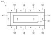
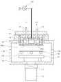
도 1은 본 발명의 제1 실시예에 따른 스퍼터 장치의 구조도이다.
도 2는 마그네트 유닛의 평면 구조도이다.
도 3은 도 2의 종방향 단면 구조로서의 마그네트 유닛과 타겟 간의 배치 상태도이다.
도 4는 도 2의 횡방향 단면 구조로서의 마그네트 유닛과 타겟 간의 배치 상태도이다.
도 5는 본 발명의 제2 실시예에 따른 스퍼터 장치의 구조도이다.
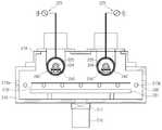
도 6은 본 발명의 제3 실시예에 따른 스퍼터 장치의 구조도이다.
도 7은 본 발명의 제4 실시예에 따른 스퍼터 장치의 구조도이다.1 is a structural diagram of a sputter apparatus according to a first embodiment of the present invention.
2 is a plan view of the magnet unit.
3 is a layout view of the magnet unit and the target as the longitudinal cross-sectional structure of FIG. 2.
FIG. 4 is a layout view of the magnet unit and the target as the lateral cross-sectional structure of FIG. 2.
5 is a structural diagram of a sputter apparatus according to a second embodiment of the present invention.
6 is a structural diagram of a sputtering apparatus according to a third embodiment of the present invention.
7 is a structural diagram of a sputter apparatus according to a fourth embodiment of the present invention.
본 발명과 본 발명의 동작상의 이점 및 본 발명의 실시에 의하여 달성되는 목적을 충분히 이해하기 위해서는 본 발명의 바람직한 실시예를 예시하는 첨부 도면 및 첨부 도면에 기재된 내용을 참조하여야만 한다.In order to fully understand the present invention, operational advantages of the present invention, and objects achieved by the practice of the present invention, reference should be made to the accompanying drawings and the accompanying drawings which illustrate preferred embodiments of the present invention.
이하, 첨부도면을 참조하여 본 발명의 바람직한 실시예를 설명함으로써, 본 발명을 상세히 설명한다. 각 도면에 제시된 동일한 참조부호는 동일한 부재를 나타낸다.DETAILED DESCRIPTION OF THE PREFERRED EMBODIMENTS Hereinafter, preferred embodiments of the present invention will be described in detail with reference to the accompanying drawings. Like reference symbols in the drawings denote like elements.
도면 대비 설명에 앞서, 이하에서 설명될 기판이란 LCD(Liquid Crystal Display), PDP(Plasma Display Panel) 및 OLED(Organic Light Emitting Diodes) 등의 평면디스플레이 기판이거나 아니면 태양전지용 기판, 혹은 반도체 웨이퍼 기판일 수 있는데, 이하에서는 별도의 구분 없이 기판이라는 용어로 통일하도록 한다.Prior to the description of the drawings, the substrate to be described below may be a planar display substrate such as a liquid crystal display (LCD), a plasma display panel (PDP) and organic light emitting diodes (OLED), a solar cell substrate, or a semiconductor wafer substrate. However, hereinafter will be unified in the term substrate without any separate.
도 1은 본 발명의 제1 실시예에 따른 스퍼터 장치의 구조도이고, 도 2는 마그네트 유닛의 평면 구조도이며, 도 3은 도 2의 종방향 단면 구조로서의 마그네트 유닛과 타겟 간의 배치 상태도이고, 도 4는 도 2의 횡방향 단면 구조로서의 마그네트 유닛과 타겟 간의 배치 상태도이다.1 is a structural diagram of a sputtering apparatus according to a first embodiment of the present invention, FIG. 2 is a plan structural diagram of a magnet unit, FIG. 3 is a layout view of a magnet unit and a target as a longitudinal cross-sectional structure of FIG. 2 is an arrangement state diagram between the magnet unit and the target as the lateral cross-sectional structure of FIG. 2.
이들 도면에 도시된 바와 같이, 본 실시예의 스퍼터 장치는, 챔버 바디(110, chamber body)와, 챔버 바디(110) 내에 마련되어 기판을 이송 가능하게 지지하는 기판 이송 지지부(130)와, 챔버 바디(110)의 상부 영역에 마련되어 기판 이송 지지부(130) 상에서 증착 위치에 놓인 기판을 향하여 증착 물질을 제공하는 스퍼터 소스(sputter source)로서의 타겟(140)과, 타겟(140)의 일측에 배치되어 기판과의 사이에 증착을 위한 자기장(도 3 및 도 4의 자기장선 참조)을 발생시키는 마그네트 유닛(150)을 포함한다.As shown in these figures, the sputtering apparatus of this embodiment includes a
챔버 바디(110)는 외관 벽체를 형성하는 부분으로서 증착 공정 시 그 내부는 밀폐되고 고진공 상태를 유지한다. 이를 위해, 챔버 바디(110)의 하부 영역에는 게이트 밸브(111)가 마련되고, 게이트 밸브(111) 영역에는 진공 펌프(112)가 마련된다. 이에, 게이트 밸브(111)가 개방된 상태에서 진공 펌프(112)로부터의 진공압이 발생되면 챔버 바디(110)의 내부는 고진공 상태를 유지할 수 있다.The
챔버 바디(110)의 일측벽에는 챔버 바디(110)의 내부로 기판이 인입되는 기판입구(113a)가 형성되고 챔버 바디(110)의 타측벽에는 챔버 바디(110)로부터의 기판이 인출되는 기판출구(113b)가 형성된다. 기판입구(113a)와 기판출구(113b)에도 별도의 게이트 밸브가 마련될 수 있다.A substrate inlet 113a through which a substrate is introduced into the
챔버 바디(110)의 상부 영역에는 타겟(140)과 마그네트 유닛(150) 영역을 외부에서 둘러싸는 형태로 챔버 바디(110)와 결합되는 커버(114)가 마련된다. 본 실시예의 경우, 챔버 바디(110) 내에 두 개의 타겟(140)과 마그네트 유닛(150)이 마련되고 있으므로 커버(114)는 타겟(140)과 마그네트 유닛(150)이 위치된 두 군데의 영역에서 챔버 바디(110)의 상부로 솟은 형태를 취한다. 이 경우, 커버(114)들은 리드(115, lid)에 의해 상호 기밀하게 연결된다. 물론, 본 발명의 권리범위가 이에 제한될 필요는 없으므로 타겟(140)과 마그네트 유닛(150)은 하나씩 마련될 수도 있다.A
기판 이송 지지부(130)는 챔버 바디(110) 내의 중앙 영역에 배치되어 기판을 지지함과 동시에 기판입구(113a)로 인입된 기판을 기판출구(113b)로 이송시키는 역할을 한다.The substrate
기판 이송 지지부(130)는 롤러로 적용될 수 있는데, 통상 챔버 바디(110)의 내부가 고온 상태를 유지한다는 점을 감안할 때 기판 이송 지지부(130)는 내열성 및 내구성이 우수한 재질로 제작되는 것이 바람직하다.The
이러한 기판 이송 지지부(130)의 하부 영역에는 기판 이송 지지부(130) 상에 놓인 기판을, 특히 기판의 증착면을 가열하는 히터(131)가 마련된다. 히터(131)는 타겟(140)으로부터 제공되는 증착 물질이 기판에 잘 증착될 수 있도록 기판을 수백도 이상으로 가열하는 역할을 한다. 이러한 히터(131)는 기판의 전면을 골고루, 또한 급속으로 가열할 수 있도록 기판의 사이즈와 유사하거나 그보다 큰 사이즈를 가질 수 있다.The lower region of the
타겟(140)은 챔버 바디(110)의 상부 영역에 마련되어 기판 이송 지지부(130) 상에서 증착 위치에 놓인 기판을 향하여 증착 물질을 제공하는 스퍼터 소스(sputter source)의 역할을 한다.The
통상적으로 타겟(140)과 마그네트 유닛(150) 영역이 음극(cathode)을 형성하고 기판 영역이 양극(anode)을 형성한다. 본 실시예에서 타겟(140)은 평면 타입의 타겟(140), 즉 고정된 해당 위치에서 하부 영역의 기판을 향해 증착 물질을 제공하는 평면 타입의 타겟(140)으로 마련된다.Typically, the region of the
타겟(140)이 설치되기 위해, 또한 마그네트 유닛(150)이 기밀하게 설치되기 위해, 마그네트 유닛(150)을 둘러싸는 형태로 캐소드 백킹 플레이트(120, cathode backing plate)가 마련된다. 캐소드 백킹 플레이트(120)는 RF 또는 DC 전원의 파워(123, power)와 연결된다. 캐소드 백킹 플레이트(120)와 커버(114) 사이에는 이들 사이를 기밀유지시키는 캐소드 인슐레이터(121, cathode insulator)가 마련된다.In order to install the
이러한 구조에서 타겟(140)은 기판을 향한 캐소드 백킹 플레이트(120)의 표면 일측에 결합되는데, 챔버 바디(110)와 캐소드 백킹 플레이트(120) 사이에는 증착 물질이 캐소드 백킹 플레이트(120) 쪽으로 향하는 것을 저지하는 쉴드(122, shield)가 마련된다. 쉴드(122)는 타겟(140)을 제외한 캐소드 백킹 플레이트(120)의 외부 영역을 둘러싸는 형태로 커버(114)에 결합될 수 있다. 타겟(140) 영역의 냉각을 위하여 챔버 바디(110)의 외측에서 냉각수 유입관(124)과 냉각수 배출관(125)이 캐소드 백킹 플레이트(120)의 내부와 연결된다.In this structure, the
한편, 마그네트 유닛(150)은 타겟(140)의 일측, 다시 말해 캐소드 백킹 플레이트(120)의 내부에 배치되어 기판과의 사이에 증착을 위한 자기장(도 3 및 도 4의 자기장선 참조)을 발생시키는 역할을 한다.On the other hand, the
이러한 마그네트 유닛(150)은 도 2 내지 도 4에 도시된 바와 같이, 적어도 일 방향으로 위치 이동 가능한 다수의 마그네트(161~163)와, 다수의 마그네트(161~163)에 대한 베이스(base)를 형성하는 베이스 폴 플레이트(170)와, 베이스 폴 플레이트(170)에 대해 다수의 마그네트(161~163)를 개별적으로 지지하는 개별 폴 플레이트(181~183)를 구비한다.As shown in FIGS. 2 to 4, the
다수의 마그네트(161~163)는 베이스 폴 플레이트(170)의 중앙 영역에 배치되는 중심부 마그네트(161)와, 중심부 마그네트(161)의 외곽에서 중심부 마그네트(161)의 외곽에 배치되는 외곽부 마그네트(162,163)를 구비한다.The plurality of
이때, 외곽부 마그네트(162,163)는 외곽부 마그네트(162,163)에 대한 그 돌출 높이가 중심부 마그네트(161)보다 낮거나 혹은 중심부 마그네트(161)의 사이즈보다 부피가 작게 마련된다. 이는 자기장의 흐름 또는 세기를 고려한 디자인인데, 경우에 따라 변경될 수도 있다. 외곽부 마그네트(162,163)들은 도 2에 도시된 바와 같이, 위치별로 그 사이즈가 다르게 마련될 수 있다.In this case, the
베이스 폴 플레이트(170)는 개별 폴 플레이트(181~183)를 통해 다수의 마그네트(161~163)를 지지하는 부분이다. 베이스 폴 플레이트(170)로 인해 개별 폴 플레이트(181~183)와 다수의 마그네트(161~163)는 일체형의 한 유닛 구조를 형성할 수 있다. 도면에 보면 베이스 폴 플레이트(170)의 두께가 개별 폴 플레이트(181~183)의 두께보다 두껍게 도시되어 있지만 본 발명의 권리범위가 이에 제한될 필요는 없다.The
개별 폴 플레이트(181~183)는 베이스 폴 플레이트(170)에 대하여 마그네트(161~163)들을 개별적으로 지지하는 부분이다. 예컨대 도 2처럼 중심부 마그네트(161)와 외곽부 마그네트(162,163)의 개수가 11개라면 개별 폴 플레이트(181~183) 역시 11개가 마련되어 해당 위치에서 마그네트(161~163)들을 개별적으로 지지한다. 따라서 마그네트(161~163)들과 개별 폴 플레이트(181~183)들은 상호간 대응되는 것끼리 결합되어 있어야 하는데 이들은 접착 방식에 의해 결합될 수 있다.The
한편, 마그네트(161~163)들을 개별적으로 지지하는 개별 폴 플레이트(181~183)들은 다수의 세팅볼트(191,192)에 의해 베이스 폴 플레이트(170)에 체결될 수 있다.Meanwhile, the
이때, 다수의 세팅볼트(191,192)는 그 위치 또는 기능에 따라 베이스 폴 플레이트(170)와 개별 폴 플레이트(181~183)를 상호간 체결시키는 체결볼트(191)와, 베이스 폴 플레이트(170)에 대해 개별 폴 플레이트(181~183)의 갭 또는 각도를 조절하는 조절볼트(192)로 나뉠 수 있다.In this case, the plurality of setting
예컨대, 사이즈가 가장 큰 중심부 마그네트(161)를 그 예로 들면, 중심부 마그네트(161)의 개별 폴 플레이트(181)에는 체결볼트(191)를 사이에 두고 양측에 조절볼트(192)가 결합될 수 있다. 물론, 사이즈에 따라 중심부 마그네트(161)에 마련되는 체결볼트(191)와 조절볼트(192)의 개수는 더 증가될 수도 있다.For example, the
그리고 도면에는 단면의 위치상 외곽부 마그네트(162,163)들에 조절볼트(192)만이 도시되어 있지만 외곽부 마그네트(162,163)들에도 체결볼트(191)와 조절볼트(192)가 결합될 수 있다.In addition, although only the adjusting
이처럼 체결볼트(191)와 조절볼트(192)가 마련되는 경우, 조절볼트(192)를 먼저 조절하여 베이스 폴 플레이트(170)에 대해 개별 폴 플레이트(181~183)의 갭 또는 각도를 조절한 상태에서 체결볼트(191)를 통해 베이스 폴 플레이트(170)에 대해 개별 폴 플레이트(181~183)를 견고하게 고정시키면 된다.When the
물론, 도 3 및 도 4의 그림은 하나의 예시에 불과하므로 만약 조절의 기능을 수행하면서 체결할 수 있는 볼트라면 베이스 폴 플레이트(170)와 모든 개별 폴 플레이트(181~183)에 하나씩의 체결볼트(191) 혹은 조절볼트(192)만이 결합되어도 좋고, 아니면 체결볼트(191)와 조절볼트(192)가 하나씩 혹은 다수 개씩 결합되어도 좋다.Of course, Figure 3 and Figure 4 is only one example, so if the bolt that can be tightened while performing the function of adjustment, one fastening bolt on the
어떠한 조합을 갖더라도 본 실시예의 마그네트 유닛(150)의 경우에는 마그네트(161~163)들을 개별적으로 지지하는 개별 폴 플레이트(181~183)가 베이스 폴 플레이트(170)에 대해 조절될 수 있기 때문에, 도 3 및 도 4처럼 타겟(140)에 대한 마그네트(161~163)들의 간격(L1,L2,L3) 조정이 자유롭다.In the case of the
때문에 타겟(140)과의 간격, 타겟(140)의 재질 및 두께 등의 요인에 따라 달라질 수 있는 자기장의 세기 등에 기초한 시뮬레이션을 통해 마그네트(161~163)들의 위치를 세팅하는 세팅 작업을 용이하게 수행할 수 있게 되고, 이에 따라 종래기술 대비 마그네트(161~163)들의 세팅 작업에 따른 실패 비용 및 시간 손실을 현저하게 감소시킬 수 있게 되는 것이다.Therefore, the setting operation for setting the positions of the
참고로, 타겟(140)에 대한 마그네트(161~163)들의 간격(L1,L2,L3) 조정이란 타겟(140)에 대한 마그네트(161~163)들의 직진 거리만을 의미하지는 않는다. 예컨대, 도 3 및 도 4의 도면과 달리, 조절볼트(192)들이 개별 폴 플레이트(181~183)의 중앙 영역에서 일측으로 편심된 위치에 배치될 경우라면 타겟(140)에 대한 마그네트(161~163)들이 약간 경사진 방향으로 접근될 것인데, 이러한 조정 작업 역시 필요에 따라 충분히 수행될 수 있을 것이다.For reference, adjusting the distances L1, L2, and L3 of the
이러한 구성을 갖는 스퍼터 장치의 작용에 대해 설명하면 다음과 같다.The operation of the sputtering device having such a configuration will be described below.
우선, 타겟(140)의 재질 및 두께 등의 요인에 따라 달라질 수 있는 자기장의 세기 등에 기초한 시뮬레이션을 통해 마그네트(161~163)들의 위치를 세팅한다. 즉 마그네트(161~163)들의 위치 세팅 시 자기장의 세기 등에 기초한 시뮬레이션을 통해 조절볼트(192)로 먼저 마그네트(161~163)들의 위치를 잡은 후에 체결볼트(191)로 체결하면 되는데, 이처럼 세팅 작업이 용이하기 때문에 종래기술 대비 마그네트(161~163)들의 세팅 작업에 따른 실패 비용 및 시간 손실을 현저하게 감소시킬 수 있게 된다.First, the positions of the
도 1과 같이 장치의 조립이 세팅되고 나면, 챔버 바디(110)의 기판입구(113a)를 통해 기판이 유입되어 기판 이송 지지부(130) 상의 증착 위치로 배치되고 증착 공정이 개시된다. 즉 챔버 바디(110) 내로 예컨대 아르곤(Ar) 가스가 충진되고, 챔버 바디(110)는 그 내부가 밀폐되면서 고진공을 유지한다.After the assembly of the apparatus is set as shown in FIG. 1, the substrate is introduced through the
이 상태에서 파워(123)로부터 타겟(140) 쪽에 음극 전압이 가해지면, 타겟(140)으로부터 방출된 전자들이 아르곤(Ar) 가스와 충돌하여 아르곤(Ar) 가스가 이온화된다.In this state, when a negative voltage is applied from the
이온화된 아르곤(Ar) 가스는 전위차에 의해 타겟(140) 방향으로 가속되어 타겟(140)의 표면과 충돌하게 되고, 이때 타겟(140) 원자, 즉 증착 물질이 타겟(140)으로부터 발생되어 기판의 증착면에 떨어지면서 기판의 증착 공정이 진행된다.The ionized argon (Ar) gas is accelerated toward the
증착 공정이 완료되면, 챔버 바디(110) 내의 진공이 해제되고 기판출구(113b)가 열리면서 기판출구(113b)를 통해 기판이 취출되고, 다시 새로운 기판이 기판입구(113a) 쪽으로 유입되어 증착 공정을 진행하게 된다.When the deposition process is completed, the vacuum in the
이와 같이, 본 실시예에 따르면, 타겟(140)에 대한 마그네트(161~163)들의 위치를 손쉽게 조정하면서 세팅할 수 있어 종래기술 대비 마그네트(161~163)들의 세팅 작업에 따른 실패 비용 및 시간 손실을 현저하게 감소시킬 수 있게 된다.As described above, according to the present exemplary embodiment, it is possible to easily set the positions of the
도 5는 본 발명의 제2 실시예에 따른 스퍼터 장치의 구조도이고, 도 6은 본 발명의 제3 실시예에 따른 스퍼터 장치의 구조도이다.5 is a structural diagram of a sputtering apparatus according to a second embodiment of the present invention, and FIG. 6 is a structural diagram of a sputtering apparatus according to a third embodiment of the present invention.
도 5의 경우에는 타겟(140a)과 마그네트 유닛(150a)이 각각 하나씩 마련되는 스퍼터 장치에 관한 도면이다. 그리고 도 6의 경우에는 도 1처럼 타겟(140b)과 마그네트 유닛(150b)이 각각 두개씩 마련되되 도 1과는 달리 이들이 하부에 배치되고 반대로 기판이 상부에 배치되는 구조를 갖는 스퍼터 장치에 관한 도면이다. 도 5 및 도 6과 같은 스퍼터 장치의 경우에도 본 발명의 효과를 제공하는 데에는 아무런 무리가 없다.5 illustrates a sputtering device in which one
도 7은 본 발명의 제4 실시예에 따른 스퍼터 장치의 구조도이다.7 is a structural diagram of a sputter apparatus according to a fourth embodiment of the present invention.
본 실시예는 회전 타입의 타겟(240)을 구비하는 스퍼터 장치에 대한 도면이다. 대부분의 구성은 제1 실시예와 동일하다. 따라서 도 7에 대한 자세한 설명은 생략하는 대신에 제1 실시예와 대응되는 부분에 참조부호가 200번대로 시작하도록 도면부호를 부여하였다.This embodiment is a diagram of a sputtering device having a
도 7과 같은 회전 타입의 타겟(240)은 타겟(240)이 회전하면서 증착 물질을 발생시키기 때문에 제1 실시예보다 증착 시간 및 효율을 상대적으로 더 높일 수 있는 이점이 있다.Since the
이처럼 회전 타입의 타겟(240)이 적용되더라도 그 일측에는 마그네트 유닛(250)이 마련되는데, 마그네트 유닛(250)은 도 2 내지 도 4에서 설명한 것 그대로를 적용할 수 있다. 다만, 본 실시예의 경우에는 마그네트 유닛(250)을 중심으로 하여 타겟(240)이 원주 방향으로 배치되는 형태를 가지므로 마그네트 유닛(250) 내의 마그네트(161~163, 도 2 내지 도 4 참조)의 위치 조정은 전술한 실시예보다 좀 더 세밀하게, 즉 직진 방향뿐만 아니라 곡선 방향으로도 위치가 조정될 수 있도록 하는 것이 유리하다. 이의 구조는 조절볼트(192, 도 2 내지 도 4 참조)의 위치를 변경시킴으로써 간단하게 구현할 수 있으므로 생략하였다.As described above, even when the
본 실시예처럼 구현하더라도 타겟(240)에 대한 마그네트(161~163)들의 위치를 손쉽게 조정하면서 세팅할 수 있어 종래기술 대비 마그네트(161~163)들의 세팅 작업에 따른 실패 비용 및 시간 손실을 현저하게 감소시킬 수 있게 된다는 본 발명의 효과를 제공하기에 충분하다.Even if implemented as in this embodiment, it is possible to easily set while setting the position of the magnets (161 ~ 163) relative to the
이와 같이 본 발명은 기재된 실시예에 한정되는 것이 아니고, 본 발명의 사상 및 범위를 벗어나지 않고 다양하게 수정 및 변형할 수 있음은 이 기술의 분야에서 통상의 지식을 가진 자에게 자명하다. 따라서 그러한 수정예 또는 변형예들은 본 발명의 특허청구범위에 속한다 하여야 할 것이다.It will be apparent to those skilled in the art that various modifications and variations can be made in the present invention without departing from the spirit or scope of the invention. Accordingly, such modifications or variations are intended to fall within the scope of the appended claims.
110 : 챔버 바디 111 : 게이트 밸브
112 : 진공 펌프 114 : 커버
115 : 리드 120 : 캐소드 백킹 플레이트
121 : 캐소드 인슐레이터 122 : 쉴드
123 : 파워 130 : 기판 이송 지지부
140 : 타겟 150 : 마그네트 유닛
161~163 : 마그네트 170 : 베이스 폴 플레이트
181~183 : 개별 폴 플레이트 191 : 체결볼트
192 : 조절볼트110: chamber body 111: gate valve
112: vacuum pump 114: cover
115: lead 120: cathode backing plate
121: cathode insulator 122: shield
123: power 130: substrate transfer support
140: target 150: magnet unit
161 to 163: Magnet 170: Base pole plate
181 ~ 183: Individual pole plate 191: Fastening bolt
192: adjusting bolt
Claims (11)
Translated fromKorean다수의 마그네트를 구비하며, 상기 타겟에 이웃하게 배치되어 상기 기판과의 사이에 증착을 위한 자기장을 발생시키는 마그네트 유닛을 포함하며,
상기 마그네트 유닛은,
상기 다수의 마그네트에 대한 베이스(base)를 형성하는 베이스 폴 플레이트;
상기 베이스 폴 플레이트에 대해 상대 위치 조정 가능하게 상기 베이스 폴 플레이트에 결합되며, 상기 다수의 마그네트가 개별적으로 각각 접착되는 다수의 개별 폴 플레이트; 및
상기 베이스 폴 플레이트에 대해 상기 개별 폴 플레이트의 갭 또는 각도를 조절하는 조절볼트와, 상기 베이스 폴 플레이트와 상기 개별 폴 플레이트를 상호간 체결시키는 체결볼트를 구비하는 다수의 세팅볼트를 포함하는 것을 특징으로 하는 스퍼터 장치.A target as a sputter source for providing a deposition material towards a substrate placed in a deposition position within the chamber body; And
A magnet unit having a plurality of magnets, the magnet unit being disposed adjacent to the target to generate a magnetic field for deposition between the substrate,
The magnet unit,
A base pole plate forming a base for the plurality of magnets;
A plurality of individual pole plates coupled to the base pole plate to be adjustable relative to the base pole plate, the plurality of magnets being individually bonded to each other; And
And a plurality of setting bolts having adjustment bolts for adjusting the gap or angle of the individual pole plates with respect to the base pole plate, and fastening bolts for fastening the base pole plate and the individual pole plates to each other. Sputter device.
상기 다수의 마그네트는,
상기 베이스 폴 플레이트의 중앙 영역에 배치되는 중심부 마그네트; 및
상기 중심부 마그네트의 외곽에서 상기 베이스 폴 플레이트의 외곽에 배치되되 상기 베이스 폴 플레이트에 대한 돌출 높이가 상기 중심부 마그네트보다 낮거나 상기 중심부 마그네트의 사이즈보다 부피가 작은 다수의 외곽부 마그네트를 포함하는 것을 특징으로 하는 스퍼터 장치.The method of claim 1,
The plurality of magnets,
A central magnet disposed in the central area of the base pole plate; And
And a plurality of outer magnets disposed at an outer side of the base pole plate at an outer side of the central magnet, the protrusion height of the base pole plate being lower than the central magnet or smaller than the size of the central magnet. Sputter device.
상기 중심부 마그네트의 개별 폴 플레이트에는 상기 체결볼트를 사이에 두고 양측에 상기 조절볼트가 결합되며,
상기 다수의 외곽부 마그네트의 개별 폴 플레이트에는 적어도 하나의 상기 조절볼트 및 적어도 하나의 상기 체결볼트가 결합되는 것을 특징으로 하는 스퍼터 장치.The method according to claim 6,
The adjusting pole is coupled to both sides of the central pole plate with the fastening bolt between the individual pole plates,
At least one adjustment bolt and at least one fastening bolt are coupled to individual pole plates of the plurality of outer magnets.
상기 다수의 외곽부 마그네트들은 위치별로 그 사이즈가 다르게 마련되는 것을 특징으로 하는 스퍼터 장치.The method according to claim 6,
Sputtering apparatus characterized in that the plurality of outer magnets are provided in a different size for each position.
상기 타겟은 평면 타입의 타겟 또는 회전 타입의 타겟인 것을 특징으로 하는 스퍼터 장치.The method of claim 1,
And the target is a planar target or a rotational target.
상기 마그네트 유닛이 내부에 마련되고 외표면의 일측에 상기 타겟이 결합되며, RF 또는 DC 전원의 파워(power)가 전기적으로 연결되는 캐소드 백킹 플레이트(cathode backing plate); 및
상기 캐소드 백킹 플레이트와 상기 챔버 바디의 상부에 마련되는 커버 사이에서 상기 캐소드 백킹 플레이트와 상기 커버를 기밀유지시키는 캐소드 인슐레이터(cathode insulator)를 더 포함하는 것을 특징으로 하는 스퍼터 장치.The method of claim 1,
A cathode backing plate having the magnet unit provided therein and having the target coupled to one side of an outer surface thereof, and having a power of an RF or DC power source electrically connected thereto; And
And a cathode insulator for hermetically holding the cathode backing plate and the cover between the cathode backing plate and the cover provided on the chamber body.
상기 타겟을 제외한 상기 캐소드 백킹 플레이트의 외부 영역을 둘러싸는 형태로 상기 커버에 결합되어 상기 캐소드 백킹 플레이트 영역으로 증착 물질이 향하는 것을 저지하는 쉴드(shield); 및
상기 타겟 영역의 냉각을 위하여 상기 챔버 바디의 외부에서 상기 캐소드 백킹 플레이트의 내부로 연통되는 냉각수 유입관 및 냉각수 배출관을 더 포함하는 것을 특징으로 하는 스퍼터 장치.The method of claim 10,
A shield coupled to the cover in a form surrounding the outer region of the cathode backing plate except for the target to prevent the deposition material from being directed to the cathode backing plate region; And
And a coolant inlet pipe and a coolant discharge pipe communicating with the inside of the cathode backing plate from the outside of the chamber body for cooling the target area.
Priority Applications (1)
| Application Number | Priority Date | Filing Date | Title |
|---|---|---|---|
| KR1020100023465AKR101209651B1 (en) | 2010-03-16 | 2010-03-16 | Apparatus to Sputter |
Applications Claiming Priority (1)
| Application Number | Priority Date | Filing Date | Title |
|---|---|---|---|
| KR1020100023465AKR101209651B1 (en) | 2010-03-16 | 2010-03-16 | Apparatus to Sputter |
Publications (2)
| Publication Number | Publication Date |
|---|---|
| KR20110104362A KR20110104362A (en) | 2011-09-22 |
| KR101209651B1true KR101209651B1 (en) | 2012-12-07 |
Family
ID=44955161
Family Applications (1)
| Application Number | Title | Priority Date | Filing Date |
|---|---|---|---|
| KR1020100023465AExpired - Fee RelatedKR101209651B1 (en) | 2010-03-16 | 2010-03-16 | Apparatus to Sputter |
Country Status (1)
| Country | Link |
|---|---|
| KR (1) | KR101209651B1 (en) |
Cited By (1)
| Publication number | Priority date | Publication date | Assignee | Title |
|---|---|---|---|---|
| KR101604977B1 (en) | 2015-02-24 | 2016-03-22 | 주식회사 아바코 | Reactive sputtering apparatus |
Families Citing this family (2)
| Publication number | Priority date | Publication date | Assignee | Title |
|---|---|---|---|---|
| KR101379221B1 (en)* | 2012-06-29 | 2014-04-07 | 한밭대학교 산학협력단 | Fabrication method of SiCx Passivation layer and Solar cell usint the same |
| KR102152706B1 (en)* | 2014-03-06 | 2020-09-07 | 삼성전자주식회사 | Layer deposition systems and methods of forming conductive patterns using the same |
Citations (1)
| Publication number | Priority date | Publication date | Assignee | Title |
|---|---|---|---|---|
| JPS60262970A (en) | 1984-06-11 | 1985-12-26 | Ulvac Corp | Cathode apparatus for magnetic material target |
- 2010
- 2010-03-16KRKR1020100023465Apatent/KR101209651B1/ennot_activeExpired - Fee Related
Patent Citations (1)
| Publication number | Priority date | Publication date | Assignee | Title |
|---|---|---|---|---|
| JPS60262970A (en) | 1984-06-11 | 1985-12-26 | Ulvac Corp | Cathode apparatus for magnetic material target |
Cited By (1)
| Publication number | Priority date | Publication date | Assignee | Title |
|---|---|---|---|---|
| KR101604977B1 (en) | 2015-02-24 | 2016-03-22 | 주식회사 아바코 | Reactive sputtering apparatus |
Also Published As
| Publication number | Publication date |
|---|---|
| KR20110104362A (en) | 2011-09-22 |
Similar Documents
| Publication | Publication Date | Title |
|---|---|---|
| KR100776861B1 (en) | Improved magnetron sputtering system for large-area substrates | |
| US7815782B2 (en) | PVD target | |
| KR101209652B1 (en) | Apparatus to Sputter | |
| JP2001192805A (en) | Inclined sputtering target with shield for blocking contaminant | |
| CN105200381B (en) | The auxiliary magnetic control sputtering film plating device of anodic field | |
| US20070056845A1 (en) | Multiple zone sputtering target created through conductive and insulation bonding | |
| KR101209651B1 (en) | Apparatus to Sputter | |
| JP5718767B2 (en) | Sputtering equipment | |
| KR101694197B1 (en) | Apparatus to sputter | |
| TWI312012B (en) | Improved magnetron sputtering system for large-area substrates having removable anodes | |
| KR101209653B1 (en) | Apparatus to Sputter | |
| KR101288133B1 (en) | Glass deposition apparatus | |
| KR101430653B1 (en) | Inline sputtering apparatus | |
| KR101125557B1 (en) | Apparatus to Sputter | |
| JP2007031817A (en) | Sputtering apparatus and sputtering method | |
| KR101341433B1 (en) | Magnetron sputtering apparatus | |
| CN102373423B (en) | Sputtering coating device | |
| KR20140099340A (en) | Sputtering apparatus and method for sputtering of oxide semiconductor material | |
| KR101988336B1 (en) | Inline sputtering apparatus | |
| KR101430660B1 (en) | Apparatus to sputter | |
| KR101385590B1 (en) | Apparatus to sputter | |
| KR101617276B1 (en) | Plasma generator and substrate treatment apparatus having thereof | |
| KR101288131B1 (en) | Glass deposition apparatus | |
| US20160099135A1 (en) | Rectangular Hollow Sputter Source and Method of use Thereof | |
| KR101687302B1 (en) | Apparatus to sputter |
Legal Events
| Date | Code | Title | Description |
|---|---|---|---|
| A201 | Request for examination | ||
| PA0109 | Patent application | St.27 status event code:A-0-1-A10-A12-nap-PA0109 | |
| PA0201 | Request for examination | St.27 status event code:A-1-2-D10-D11-exm-PA0201 | |
| P11-X000 | Amendment of application requested | St.27 status event code:A-2-2-P10-P11-nap-X000 | |
| P13-X000 | Application amended | St.27 status event code:A-2-2-P10-P13-nap-X000 | |
| R15-X000 | Change to inventor requested | St.27 status event code:A-3-3-R10-R15-oth-X000 | |
| R16-X000 | Change to inventor recorded | St.27 status event code:A-3-3-R10-R16-oth-X000 | |
| D13-X000 | Search requested | St.27 status event code:A-1-2-D10-D13-srh-X000 | |
| D14-X000 | Search report completed | St.27 status event code:A-1-2-D10-D14-srh-X000 | |
| PG1501 | Laying open of application | St.27 status event code:A-1-1-Q10-Q12-nap-PG1501 | |
| PE0902 | Notice of grounds for rejection | St.27 status event code:A-1-2-D10-D21-exm-PE0902 | |
| E13-X000 | Pre-grant limitation requested | St.27 status event code:A-2-3-E10-E13-lim-X000 | |
| P11-X000 | Amendment of application requested | St.27 status event code:A-2-2-P10-P11-nap-X000 | |
| P13-X000 | Application amended | St.27 status event code:A-2-2-P10-P13-nap-X000 | |
| E701 | Decision to grant or registration of patent right | ||
| PE0701 | Decision of registration | St.27 status event code:A-1-2-D10-D22-exm-PE0701 | |
| GRNT | Written decision to grant | ||
| PR0701 | Registration of establishment | St.27 status event code:A-2-4-F10-F11-exm-PR0701 | |
| PR1002 | Payment of registration fee | St.27 status event code:A-2-2-U10-U11-oth-PR1002 Fee payment year number:1 | |
| PG1601 | Publication of registration | St.27 status event code:A-4-4-Q10-Q13-nap-PG1601 | |
| R18-X000 | Changes to party contact information recorded | St.27 status event code:A-5-5-R10-R18-oth-X000 | |
| PN2301 | Change of applicant | St.27 status event code:A-5-5-R10-R13-asn-PN2301 St.27 status event code:A-5-5-R10-R11-asn-PN2301 | |
| PR1001 | Payment of annual fee | St.27 status event code:A-4-4-U10-U11-oth-PR1001 Fee payment year number:4 | |
| P22-X000 | Classification modified | St.27 status event code:A-4-4-P10-P22-nap-X000 | |
| FPAY | Annual fee payment | Payment date:20161117 Year of fee payment:5 | |
| PR1001 | Payment of annual fee | St.27 status event code:A-4-4-U10-U11-oth-PR1001 Fee payment year number:5 | |
| R18-X000 | Changes to party contact information recorded | St.27 status event code:A-5-5-R10-R18-oth-X000 | |
| FPAY | Annual fee payment | Payment date:20171117 Year of fee payment:6 | |
| L13-X000 | Limitation or reissue of ip right requested | St.27 status event code:A-2-3-L10-L13-lim-X000 | |
| PR1001 | Payment of annual fee | St.27 status event code:A-4-4-U10-U11-oth-PR1001 Fee payment year number:6 | |
| U15-X000 | Partial renewal or maintenance fee paid modifying the ip right scope | St.27 status event code:A-4-4-U10-U15-oth-X000 | |
| PN2301 | Change of applicant | St.27 status event code:A-5-5-R10-R13-asn-PN2301 St.27 status event code:A-5-5-R10-R11-asn-PN2301 | |
| L13-X000 | Limitation or reissue of ip right requested | St.27 status event code:A-2-3-L10-L13-lim-X000 | |
| PR1001 | Payment of annual fee | St.27 status event code:A-4-4-U10-U11-oth-PR1001 Fee payment year number:7 | |
| U15-X000 | Partial renewal or maintenance fee paid modifying the ip right scope | St.27 status event code:A-4-4-U10-U15-oth-X000 | |
| FPAY | Annual fee payment | Payment date:20190930 Year of fee payment:8 | |
| PR1001 | Payment of annual fee | St.27 status event code:A-4-4-U10-U11-oth-PR1001 Fee payment year number:8 | |
| PC1903 | Unpaid annual fee | St.27 status event code:A-4-4-U10-U13-oth-PC1903 Not in force date:20201204 Payment event data comment text:Termination Category : DEFAULT_OF_REGISTRATION_FEE | |
| R18-X000 | Changes to party contact information recorded | St.27 status event code:A-5-5-R10-R18-oth-X000 | |
| PC1903 | Unpaid annual fee | St.27 status event code:N-4-6-H10-H13-oth-PC1903 Ip right cessation event data comment text:Termination Category : DEFAULT_OF_REGISTRATION_FEE Not in force date:20201204 |