KR101209003B1 - Method and apparatus for manufacturing memory device having 3 dimensional structure - Google Patents
Method and apparatus for manufacturing memory device having 3 dimensional structureDownload PDFInfo
- Publication number
- KR101209003B1 KR101209003B1KR1020100100092AKR20100100092AKR101209003B1KR 101209003 B1KR101209003 B1KR 101209003B1KR 1020100100092 AKR1020100100092 AKR 1020100100092AKR 20100100092 AKR20100100092 AKR 20100100092AKR 101209003 B1KR101209003 B1KR 101209003B1
- Authority
- KR
- South Korea
- Prior art keywords
- substrate
- insulating layer
- layer
- silicon oxide
- sacrificial layer
- Prior art date
- Legal status (The legal status is an assumption and is not a legal conclusion. Google has not performed a legal analysis and makes no representation as to the accuracy of the status listed.)
- Active
Links
- 238000004519manufacturing processMethods0.000titleclaimsabstractdescription30
- 238000000034methodMethods0.000titleclaimsdescription39
- 239000000758substrateSubstances0.000claimsabstractdescription124
- VYPSYNLAJGMNEJ-UHFFFAOYSA-NSilicium dioxideChemical compoundO=[Si]=OVYPSYNLAJGMNEJ-UHFFFAOYSA-N0.000claimsabstractdescription43
- 229910052814silicon oxideInorganic materials0.000claimsabstractdescription41
- 238000000151depositionMethods0.000claimsabstractdescription21
- MROCJMGDEKINLD-UHFFFAOYSA-NdichlorosilaneChemical compoundCl[SiH2]ClMROCJMGDEKINLD-UHFFFAOYSA-N0.000claimsabstractdescription19
- 230000000149penetrating effectEffects0.000claimsabstractdescription15
- 239000007789gasSubstances0.000claimsdescription38
- 238000003825pressingMethods0.000claimsdescription13
- 238000005530etchingMethods0.000claimsdescription11
- 125000001495ethyl groupChemical group[H]C([H])([H])C([H])([H])*0.000claimsdescription8
- OAICVXFJPJFONN-UHFFFAOYSA-NPhosphorusChemical compound[P]OAICVXFJPJFONN-UHFFFAOYSA-N0.000claimsdescription5
- AUEPDNOBDJYBBK-UHFFFAOYSA-N[Si].[C-]#[O+]Chemical group[Si].[C-]#[O+]AUEPDNOBDJYBBK-UHFFFAOYSA-N0.000claimsdescription5
- 125000002496methyl groupChemical group[H]C([H])([H])*0.000claimsdescription5
- 229910052698phosphorusInorganic materials0.000claimsdescription5
- 239000011574phosphorusSubstances0.000claimsdescription5
- ZOXJGFHDIHLPTG-UHFFFAOYSA-NBoronChemical compound[B]ZOXJGFHDIHLPTG-UHFFFAOYSA-N0.000claimsdescription4
- 229910052796boronInorganic materials0.000claimsdescription4
- 239000000463materialSubstances0.000claimsdescription3
- 229910010293ceramic materialInorganic materials0.000claimsdescription2
- 239000010408filmSubstances0.000description15
- 239000004065semiconductorSubstances0.000description13
- 239000010409thin filmSubstances0.000description13
- BLRPTPMANUNPDV-UHFFFAOYSA-NSilaneChemical compound[SiH4]BLRPTPMANUNPDV-UHFFFAOYSA-N0.000description6
- 229910000077silaneInorganic materials0.000description6
- 238000003860storageMethods0.000description5
- 239000012495reaction gasSubstances0.000description4
- 229910004298SiO 2Inorganic materials0.000description3
- 230000008021depositionEffects0.000description3
- GQPLMRYTRLFLPF-UHFFFAOYSA-NNitrous OxideChemical compound[O-][N+]#NGQPLMRYTRLFLPF-UHFFFAOYSA-N0.000description2
- 239000012535impuritySubstances0.000description2
- 238000009413insulationMethods0.000description2
- 238000000206photolithographyMethods0.000description2
- 229910021420polycrystalline siliconInorganic materials0.000description2
- 229920005591polysiliconPolymers0.000description2
- XUIMIQQOPSSXEZ-UHFFFAOYSA-NSiliconChemical compound[Si]XUIMIQQOPSSXEZ-UHFFFAOYSA-N0.000description1
- 229910000577Silicon-germaniumInorganic materials0.000description1
- RGNPXDXWLDQLRA-UHFFFAOYSA-N[B].[P].[B]Chemical compound[B].[P].[B]RGNPXDXWLDQLRA-UHFFFAOYSA-N0.000description1
- LEVVHYCKPQWKOP-UHFFFAOYSA-N[Si].[Ge]Chemical compound[Si].[Ge]LEVVHYCKPQWKOP-UHFFFAOYSA-N0.000description1
- 230000015572biosynthetic processEffects0.000description1
- 230000000903blocking effectEffects0.000description1
- 238000005229chemical vapour depositionMethods0.000description1
- 239000011248coating agentSubstances0.000description1
- 238000000576coating methodMethods0.000description1
- 150000001875compoundsChemical class0.000description1
- 239000013078crystalSubstances0.000description1
- 238000009826distributionMethods0.000description1
- 229910052732germaniumInorganic materials0.000description1
- GNPVGFCGXDBREM-UHFFFAOYSA-Ngermanium atomChemical compound[Ge]GNPVGFCGXDBREM-UHFFFAOYSA-N0.000description1
- 230000010354integrationEffects0.000description1
- 238000007747platingMethods0.000description1
- 229910052710siliconInorganic materials0.000description1
- 239000010703siliconSubstances0.000description1
- 235000012239silicon dioxideNutrition0.000description1
- 239000000377silicon dioxideSubstances0.000description1
- 239000000126substanceSubstances0.000description1
- 230000005641tunnelingEffects0.000description1
- 238000001039wet etchingMethods0.000description1
Images


Classifications
- H—ELECTRICITY
- H01—ELECTRIC ELEMENTS
- H01L—SEMICONDUCTOR DEVICES NOT COVERED BY CLASS H10
- H01L21/00—Processes or apparatus adapted for the manufacture or treatment of semiconductor or solid state devices or of parts thereof
- H01L21/02—Manufacture or treatment of semiconductor devices or of parts thereof
- H01L21/04—Manufacture or treatment of semiconductor devices or of parts thereof the devices having potential barriers, e.g. a PN junction, depletion layer or carrier concentration layer
- H01L21/18—Manufacture or treatment of semiconductor devices or of parts thereof the devices having potential barriers, e.g. a PN junction, depletion layer or carrier concentration layer the devices having semiconductor bodies comprising elements of Group IV of the Periodic Table or AIIIBV compounds with or without impurities, e.g. doping materials
- H01L21/30—Treatment of semiconductor bodies using processes or apparatus not provided for in groups H01L21/20 - H01L21/26
- H01L21/302—Treatment of semiconductor bodies using processes or apparatus not provided for in groups H01L21/20 - H01L21/26 to change their surface-physical characteristics or shape, e.g. etching, polishing, cutting
- H01L21/306—Chemical or electrical treatment, e.g. electrolytic etching
- H—ELECTRICITY
- H10—SEMICONDUCTOR DEVICES; ELECTRIC SOLID-STATE DEVICES NOT OTHERWISE PROVIDED FOR
- H10D—INORGANIC ELECTRIC SEMICONDUCTOR DEVICES
- H10D88/00—Three-dimensional [3D] integrated devices
- C—CHEMISTRY; METALLURGY
- C23—COATING METALLIC MATERIAL; COATING MATERIAL WITH METALLIC MATERIAL; CHEMICAL SURFACE TREATMENT; DIFFUSION TREATMENT OF METALLIC MATERIAL; COATING BY VACUUM EVAPORATION, BY SPUTTERING, BY ION IMPLANTATION OR BY CHEMICAL VAPOUR DEPOSITION, IN GENERAL; INHIBITING CORROSION OF METALLIC MATERIAL OR INCRUSTATION IN GENERAL
- C23C—COATING METALLIC MATERIAL; COATING MATERIAL WITH METALLIC MATERIAL; SURFACE TREATMENT OF METALLIC MATERIAL BY DIFFUSION INTO THE SURFACE, BY CHEMICAL CONVERSION OR SUBSTITUTION; COATING BY VACUUM EVAPORATION, BY SPUTTERING, BY ION IMPLANTATION OR BY CHEMICAL VAPOUR DEPOSITION, IN GENERAL
- C23C16/00—Chemical coating by decomposition of gaseous compounds, without leaving reaction products of surface material in the coating, i.e. chemical vapour deposition [CVD] processes
- C23C16/44—Chemical coating by decomposition of gaseous compounds, without leaving reaction products of surface material in the coating, i.e. chemical vapour deposition [CVD] processes characterised by the method of coating
- C23C16/458—Chemical coating by decomposition of gaseous compounds, without leaving reaction products of surface material in the coating, i.e. chemical vapour deposition [CVD] processes characterised by the method of coating characterised by the method used for supporting substrates in the reaction chamber
- C23C16/4582—Rigid and flat substrates, e.g. plates or discs
- C23C16/4583—Rigid and flat substrates, e.g. plates or discs the substrate being supported substantially horizontally
- C23C16/4585—Devices at or outside the perimeter of the substrate support, e.g. clamping rings, shrouds
- H—ELECTRICITY
- H01—ELECTRIC ELEMENTS
- H01L—SEMICONDUCTOR DEVICES NOT COVERED BY CLASS H10
- H01L21/00—Processes or apparatus adapted for the manufacture or treatment of semiconductor or solid state devices or of parts thereof
- H01L21/02—Manufacture or treatment of semiconductor devices or of parts thereof
- H01L21/02104—Forming layers
- H01L21/02107—Forming insulating materials on a substrate
- H01L21/02109—Forming insulating materials on a substrate characterised by the type of layer, e.g. type of material, porous/non-porous, pre-cursors, mixtures or laminates
- H01L21/02112—Forming insulating materials on a substrate characterised by the type of layer, e.g. type of material, porous/non-porous, pre-cursors, mixtures or laminates characterised by the material of the layer
- H01L21/02123—Forming insulating materials on a substrate characterised by the type of layer, e.g. type of material, porous/non-porous, pre-cursors, mixtures or laminates characterised by the material of the layer the material containing silicon
- H01L21/02126—Forming insulating materials on a substrate characterised by the type of layer, e.g. type of material, porous/non-porous, pre-cursors, mixtures or laminates characterised by the material of the layer the material containing silicon the material containing Si, O, and at least one of H, N, C, F, or other non-metal elements, e.g. SiOC, SiOC:H or SiONC
- H01L21/02129—Forming insulating materials on a substrate characterised by the type of layer, e.g. type of material, porous/non-porous, pre-cursors, mixtures or laminates characterised by the material of the layer the material containing silicon the material containing Si, O, and at least one of H, N, C, F, or other non-metal elements, e.g. SiOC, SiOC:H or SiONC the material being boron or phosphorus doped silicon oxides, e.g. BPSG, BSG or PSG
- H—ELECTRICITY
- H01—ELECTRIC ELEMENTS
- H01L—SEMICONDUCTOR DEVICES NOT COVERED BY CLASS H10
- H01L21/00—Processes or apparatus adapted for the manufacture or treatment of semiconductor or solid state devices or of parts thereof
- H01L21/02—Manufacture or treatment of semiconductor devices or of parts thereof
- H01L21/02104—Forming layers
- H01L21/02107—Forming insulating materials on a substrate
- H01L21/02109—Forming insulating materials on a substrate characterised by the type of layer, e.g. type of material, porous/non-porous, pre-cursors, mixtures or laminates
- H01L21/02112—Forming insulating materials on a substrate characterised by the type of layer, e.g. type of material, porous/non-porous, pre-cursors, mixtures or laminates characterised by the material of the layer
- H01L21/02123—Forming insulating materials on a substrate characterised by the type of layer, e.g. type of material, porous/non-porous, pre-cursors, mixtures or laminates characterised by the material of the layer the material containing silicon
- H01L21/02164—Forming insulating materials on a substrate characterised by the type of layer, e.g. type of material, porous/non-porous, pre-cursors, mixtures or laminates characterised by the material of the layer the material containing silicon the material being a silicon oxide, e.g. SiO2
- H—ELECTRICITY
- H01—ELECTRIC ELEMENTS
- H01L—SEMICONDUCTOR DEVICES NOT COVERED BY CLASS H10
- H01L21/00—Processes or apparatus adapted for the manufacture or treatment of semiconductor or solid state devices or of parts thereof
- H01L21/02—Manufacture or treatment of semiconductor devices or of parts thereof
- H01L21/02104—Forming layers
- H01L21/02107—Forming insulating materials on a substrate
- H01L21/02109—Forming insulating materials on a substrate characterised by the type of layer, e.g. type of material, porous/non-porous, pre-cursors, mixtures or laminates
- H01L21/02205—Forming insulating materials on a substrate characterised by the type of layer, e.g. type of material, porous/non-porous, pre-cursors, mixtures or laminates the layer being characterised by the precursor material for deposition
- H01L21/02208—Forming insulating materials on a substrate characterised by the type of layer, e.g. type of material, porous/non-porous, pre-cursors, mixtures or laminates the layer being characterised by the precursor material for deposition the precursor containing a compound comprising Si
- H01L21/02211—Forming insulating materials on a substrate characterised by the type of layer, e.g. type of material, porous/non-porous, pre-cursors, mixtures or laminates the layer being characterised by the precursor material for deposition the precursor containing a compound comprising Si the compound being a silane, e.g. disilane, methylsilane or chlorosilane
- H—ELECTRICITY
- H01—ELECTRIC ELEMENTS
- H01L—SEMICONDUCTOR DEVICES NOT COVERED BY CLASS H10
- H01L21/00—Processes or apparatus adapted for the manufacture or treatment of semiconductor or solid state devices or of parts thereof
- H01L21/02—Manufacture or treatment of semiconductor devices or of parts thereof
- H01L21/02104—Forming layers
- H01L21/02107—Forming insulating materials on a substrate
- H01L21/02225—Forming insulating materials on a substrate characterised by the process for the formation of the insulating layer
- H01L21/0226—Forming insulating materials on a substrate characterised by the process for the formation of the insulating layer formation by a deposition process
- H01L21/02263—Forming insulating materials on a substrate characterised by the process for the formation of the insulating layer formation by a deposition process deposition from the gas or vapour phase
- H01L21/02271—Forming insulating materials on a substrate characterised by the process for the formation of the insulating layer formation by a deposition process deposition from the gas or vapour phase deposition by decomposition or reaction of gaseous or vapour phase compounds, i.e. chemical vapour deposition
- H—ELECTRICITY
- H01—ELECTRIC ELEMENTS
- H01L—SEMICONDUCTOR DEVICES NOT COVERED BY CLASS H10
- H01L21/00—Processes or apparatus adapted for the manufacture or treatment of semiconductor or solid state devices or of parts thereof
- H01L21/02—Manufacture or treatment of semiconductor devices or of parts thereof
- H01L21/04—Manufacture or treatment of semiconductor devices or of parts thereof the devices having potential barriers, e.g. a PN junction, depletion layer or carrier concentration layer
- H01L21/18—Manufacture or treatment of semiconductor devices or of parts thereof the devices having potential barriers, e.g. a PN junction, depletion layer or carrier concentration layer the devices having semiconductor bodies comprising elements of Group IV of the Periodic Table or AIIIBV compounds with or without impurities, e.g. doping materials
- H01L21/30—Treatment of semiconductor bodies using processes or apparatus not provided for in groups H01L21/20 - H01L21/26
- H01L21/302—Treatment of semiconductor bodies using processes or apparatus not provided for in groups H01L21/20 - H01L21/26 to change their surface-physical characteristics or shape, e.g. etching, polishing, cutting
- H01L21/306—Chemical or electrical treatment, e.g. electrolytic etching
- H01L21/30604—Chemical etching
- H—ELECTRICITY
- H01—ELECTRIC ELEMENTS
- H01L—SEMICONDUCTOR DEVICES NOT COVERED BY CLASS H10
- H01L21/00—Processes or apparatus adapted for the manufacture or treatment of semiconductor or solid state devices or of parts thereof
- H01L21/02—Manufacture or treatment of semiconductor devices or of parts thereof
- H01L21/04—Manufacture or treatment of semiconductor devices or of parts thereof the devices having potential barriers, e.g. a PN junction, depletion layer or carrier concentration layer
- H01L21/18—Manufacture or treatment of semiconductor devices or of parts thereof the devices having potential barriers, e.g. a PN junction, depletion layer or carrier concentration layer the devices having semiconductor bodies comprising elements of Group IV of the Periodic Table or AIIIBV compounds with or without impurities, e.g. doping materials
- H01L21/30—Treatment of semiconductor bodies using processes or apparatus not provided for in groups H01L21/20 - H01L21/26
- H01L21/31—Treatment of semiconductor bodies using processes or apparatus not provided for in groups H01L21/20 - H01L21/26 to form insulating layers thereon, e.g. for masking or by using photolithographic techniques; After treatment of these layers; Selection of materials for these layers
- H01L21/3105—After-treatment
- H01L21/311—Etching the insulating layers by chemical or physical means
- H01L21/31105—Etching inorganic layers
- H01L21/31111—Etching inorganic layers by chemical means
- H—ELECTRICITY
- H01—ELECTRIC ELEMENTS
- H01L—SEMICONDUCTOR DEVICES NOT COVERED BY CLASS H10
- H01L21/00—Processes or apparatus adapted for the manufacture or treatment of semiconductor or solid state devices or of parts thereof
- H01L21/67—Apparatus specially adapted for handling semiconductor or electric solid state devices during manufacture or treatment thereof; Apparatus specially adapted for handling wafers during manufacture or treatment of semiconductor or electric solid state devices or components ; Apparatus not specifically provided for elsewhere
- H01L21/67005—Apparatus not specifically provided for elsewhere
- H01L21/67011—Apparatus for manufacture or treatment
- H01L21/67017—Apparatus for fluid treatment
- H01L21/67063—Apparatus for fluid treatment for etching
- H01L21/67069—Apparatus for fluid treatment for etching for drying etching
- H—ELECTRICITY
- H10—SEMICONDUCTOR DEVICES; ELECTRIC SOLID-STATE DEVICES NOT OTHERWISE PROVIDED FOR
- H10B—ELECTRONIC MEMORY DEVICES
- H10B43/00—EEPROM devices comprising charge-trapping gate insulators
- H10B43/20—EEPROM devices comprising charge-trapping gate insulators characterised by three-dimensional arrangements, e.g. with cells on different height levels
- H10B43/23—EEPROM devices comprising charge-trapping gate insulators characterised by three-dimensional arrangements, e.g. with cells on different height levels with source and drain on different levels, e.g. with sloping channels
- H10B43/27—EEPROM devices comprising charge-trapping gate insulators characterised by three-dimensional arrangements, e.g. with cells on different height levels with source and drain on different levels, e.g. with sloping channels the channels comprising vertical portions, e.g. U-shaped channels
- H—ELECTRICITY
- H10—SEMICONDUCTOR DEVICES; ELECTRIC SOLID-STATE DEVICES NOT OTHERWISE PROVIDED FOR
- H10D—INORGANIC ELECTRIC SEMICONDUCTOR DEVICES
- H10D30/00—Field-effect transistors [FET]
- H10D30/01—Manufacture or treatment
- H10D30/021—Manufacture or treatment of FETs having insulated gates [IGFET]
- H10D30/0413—Manufacture or treatment of FETs having insulated gates [IGFET] of FETs having charge-trapping gate insulators, e.g. MNOS transistors
- H—ELECTRICITY
- H10—SEMICONDUCTOR DEVICES; ELECTRIC SOLID-STATE DEVICES NOT OTHERWISE PROVIDED FOR
- H10D—INORGANIC ELECTRIC SEMICONDUCTOR DEVICES
- H10D30/00—Field-effect transistors [FET]
- H10D30/60—Insulated-gate field-effect transistors [IGFET]
- H10D30/69—IGFETs having charge trapping gate insulators, e.g. MNOS transistors
- H10D30/693—Vertical IGFETs having charge trapping gate insulators
Landscapes
- Engineering & Computer Science (AREA)
- Physics & Mathematics (AREA)
- Condensed Matter Physics & Semiconductors (AREA)
- General Physics & Mathematics (AREA)
- Manufacturing & Machinery (AREA)
- Computer Hardware Design (AREA)
- Microelectronics & Electronic Packaging (AREA)
- Power Engineering (AREA)
- Chemical & Material Sciences (AREA)
- Chemical Kinetics & Catalysis (AREA)
- General Chemical & Material Sciences (AREA)
- Materials Engineering (AREA)
- Mechanical Engineering (AREA)
- Metallurgy (AREA)
- Organic Chemistry (AREA)
- Inorganic Chemistry (AREA)
- Semiconductor Memories (AREA)
- Non-Volatile Memory (AREA)
- Formation Of Insulating Films (AREA)
- Drying Of Semiconductors (AREA)
- Weting (AREA)
Abstract
Translated fromKoreanDescription
Translated fromKorean본 발명은 메모리 소자를 제조하는 방법 및 장치에 관한 것으로, 더욱 상세하게는 3차원 구조의 메모리 소자를 제조하는 방법 및 장치에 관한 것이다.The present invention relates to a method and apparatus for manufacturing a memory device, and more particularly, to a method and apparatus for manufacturing a memory device having a three-dimensional structure.
전자 제품은 그 부피가 점점 작아지면서도 고용량의 데이터 처리를 요하고 있다. 이에 따라, 이러한 전자 제품에 사용되는 메모리 소자의 부피를 줄이면서 그 집적도를 높일 필요가 있으며, 이러한 점에서, 종래의 평면형 구조 대신에 3차원 구조를 갖는 메모리 소자가 고려되고 있다.Electronic products are getting smaller and bulkier and require higher data throughput. Accordingly, it is necessary to increase the degree of integration while reducing the volume of memory devices used in such electronic products. In this regard, memory devices having a three-dimensional structure instead of a conventional planar structure are considered.
본 발명의 목적은 메모리 소자의 부피를 줄일 수 있는 메모리 소자를 제조하는 방법 및 장치를 제공하는 데 있다.An object of the present invention is to provide a method and apparatus for manufacturing a memory device that can reduce the volume of the memory device.
본 발명의 다른 목적은 3차원 구조의 메모리 소자를 효율적으로 제조할 수 있는 방법 및 장치를 제공하는 데 있다.Another object of the present invention is to provide a method and apparatus for efficiently manufacturing a three-dimensional memory device.
본 발명의 또 다른 목적은 복수의 박막을 증착하는 공정에서 박막의 응력 차이로 인해 발생하는 기판의 변형을 방지할 수 있는 메모리 소자를 제조하는 방법 및 장치를 제공하는 데 있다.It is still another object of the present invention to provide a method and apparatus for manufacturing a memory device capable of preventing deformation of a substrate caused by a difference in stress of a thin film in a process of depositing a plurality of thin films.
본 발명의 또 다른 목적들은 다음의 상세한 설명과 첨부한 도면으로부터 보다 명확해질 것이다.Still other objects of the present invention will become more apparent from the following detailed description and the accompanying drawings.
본 발명의 일 실시예에 의하면, 3차원 구조의 메모리 소자를 제조하는 방법은 기판 상에 하나 이상의 절연층 및 하나 이상의 희생층을 교대로 적층하는 단계; 상기 절연층 및 상기 희생층을 관통하는 관통홀을 형성하는 단계; 상기 관통홀을 채우는 패턴을 형성하는 단계; 상기 절연층 및 상기 희생층을 관통하는 개구를 형성하는 단계; 그리고 상기 개구를 통해 에천트를 공급하여 상기 희생층을 제거하는 단계를 포함하되, 상기 절연층을 적층하는 단계는 상기 기판에 SiH4, Si2H6, Si3H8, Si4H10을 포함하는 군으로부터 선택된 하나 이상의 가스를 공급하여 제1 실리콘 산화막을 증착하는 단계를 포함하며, 상기 희생층을 적층하는 단계는 상기 기판에 디클로로실란(SiCl2H2)을 공급하여 제2 실리콘 산화막을 증착하는 단계를 포함한다.According to an embodiment of the present invention, a method of manufacturing a memory device having a three-dimensional structure includes alternately stacking one or more insulating layers and one or more sacrificial layers on a substrate; Forming a through hole penetrating the insulating layer and the sacrificial layer; Forming a pattern filling the through hole; Forming an opening penetrating the insulating layer and the sacrificial layer; And removing the sacrificial layer by supplying an etchant through the opening, and stacking the insulating layer comprises SiH4 , Si2 H6 , Si3 H8 , and Si4 H10 on the substrate. Supplying at least one gas selected from the group including the depositing of the first silicon oxide layer, and depositing the sacrificial layer comprises supplying dichlorosilane (SiCl2 H2 ) to the substrate to form the second silicon oxide layer. Depositing.
상기 절연층 및 상기 희생층은 상기 에천트에 대해 식각 선택비(etch selectivity)를 가지며, 상기 희생층의 식각률은 상기 절연층의 식각률에 비해 5배 내지 300배일 수 있다.The insulating layer and the sacrificial layer may have an etch selectivity with respect to the etchant, and the etch rate of the sacrificial layer may be 5 to 300 times that of the etching layer.
상기 에천트는 HF 또는 BOE 중 어느 하나를 포함할 수 있다.The etchant may comprise either HF or BOE.
상기 절연층을 적층하는 단계는 에틸계열의 가스를 공급하는 단계를 더 포함하며, 상기 제1 실리콘 산화막은 SiCO(Silicon Carbon Oxide)일 수 있다.The stacking of the insulating layer may further include supplying an ethyl series gas, and the first silicon oxide layer may be silicon carbon oxide (SiCO).
상기 절연층을 적층하는 단계는 메틸계열의 가스를 공급하는 단계를 더 포함하며, 상기 제1 실리콘 산화막은 SiCO(Silicon Carbon Oxide)일 수 있다.The stacking of the insulating layer may further include supplying a gas of methyl series, and the first silicon oxide layer may be silicon carbon oxide (SiCO).
상기 기판의 온도는 300 내지 790도를 유지하며, 상기 기판의 공정압력은 10 mTorr 내지 250 Torr를 유지할 수 있다.The temperature of the substrate may be maintained at 300 to 790 degrees, and the process pressure of the substrate may be maintained at 10 mTorr to 250 Torr.
상기 제1 실리콘 산화막과 상기 제2 실리콘 산화막은 서로 다른 두께를 가질 수 있다.The first silicon oxide film and the second silicon oxide film may have different thicknesses.
상기 절연층 및 희생층을 교대로 적층하는 단계는 에지링을 이용하여 상기 기판의 에지부를 가압하는 단계를 더 포함할 수 있다.The alternate stacking of the insulating layer and the sacrificial layer may further include pressing an edge portion of the substrate using an edge ring.
상기 기판의 에지부는 상기 기판의 에지로부터 0.5 ㎜ 내지 3 ㎜ 내측에 해당할 수 있다.The edge portion of the substrate may correspond to 0.5 mm to 3 mm inward from the edge of the substrate.
상기 에지링은 세라믹 재질일 수 있다.The edge ring may be a ceramic material.
본 발명의 다른 실시예에 의하면, 3차원 구조의 메모리 소자를 제조하는 방법은 기판 상에 하나 이상의 절연층 및 하나 이상의 희생층을 교대로 적층하는 단계; 상기 절연층 및 상기 희생층을 관통하는 관통홀을 형성하는 단계; 상기 관통홀을 채우는 패턴을 형성하는 단계; 상기 절연층 및 상기 희생층을 관통하는 개구를 형성하는 단계; 그리고 상기 개구를 통해 에천트를 공급하여 상기 희생층을 제거하는 단계를 포함하되, 상기 절연층을 적층하는 단계는 상기 기판에 SiH4, Si2H6, Si3H8, Si4H10을 포함하는 군으로부터 선택된 하나 이상의 가스를 공급하여 제1 실리콘 산화막을 증착하는 단계를 포함하며, 상기 희생층을 적층하는 단계는 상기 기판에 SiH4, Si2H6, Si3H8, Si4H10, 디클로로실란(SiCl2H2)을 포함하는 군으로부터 선택된 하나 이상의 가스와 B2H6, PH3를 포함하는 군으로부터 선택된 하나 이상의 가스를 공급하여 보론(boron) 또는 인(phosphorus)이 주입된 제2 실리콘 산화막을 증착하는 단계를 포함한다.According to another embodiment of the present invention, a method of manufacturing a memory device having a three-dimensional structure includes alternately stacking one or more insulating layers and one or more sacrificial layers on a substrate; Forming a through hole penetrating the insulating layer and the sacrificial layer; Forming a pattern filling the through hole; Forming an opening penetrating the insulating layer and the sacrificial layer; And removing the sacrificial layer by supplying an etchant through the opening, and stacking the insulating layer comprises SiH4 , Si2 H6 , Si3 H8 , and Si4 H10 on the substrate. Supplying at least one gas selected from the group comprising the step of depositing a first silicon oxide layer, and the step of depositing the sacrificial layer is SiH4 , Si2 H6 , Si3 H8 , Si4 H10 Boron or phosphorus is injected by supplying at least one gas selected from the group containing dichlorosilane (SiCl2 H2 ) and at least one gas selected from the group containing B2 H6 , PH3 . And depositing a second silicon oxide film.
본 발명의 일 실시예에 의하면, 기판 상에 하나 이상의 절연층 및 하나 이상의 희생층을 교대로 적층하여 3차원 구조의 메모리 소자를 제조하는 장치는 기판에 대한 공정이 이루어지는 챔버; 상기 챔버 내에 설치되어 상기 기판이 놓여지는 기판지지대; 그리고 상기 기판 상에 상기 절연층을 적층할 때 상기 기판에 SiH4, Si2H6, Si3H8, Si4H10을 포함하는 군으로부터 선택된 하나 이상의 가스를 공급하며, 상기 기판 상에 상기 희생층을 적층할 때 상기 기판에 디클로로실란(SiCl2H2)을 공급하는 샤워헤드를 포함한다.According to an embodiment of the present invention, an apparatus for manufacturing a memory device having a three-dimensional structure by alternately stacking one or more insulating layers and one or more sacrificial layers on a substrate includes a chamber in which a process for a substrate is performed; A substrate support installed in the chamber and on which the substrate is placed; And supplying at least one gas selected from the group including SiH4 , Si2 H6 , Si3 H8 , and Si4 H10 to the substrate when the insulating layer is laminated on the substrate, It includes a showerhead for supplying dichlorosilane (SiCl2 H2 ) to the substrate when the sacrificial layer is laminated.
본 발명의 다른 실시예에 의하면, 기판 상에 하나 이상의 절연층 및 하나 이상의 희생층을 교대로 적층하여 3차원 구조의 메모리 소자를 제조하는 장치는 기판에 대한 공정이 이루어지는 챔버; 상기 챔버 내에 설치되어 상기 기판이 놓여지는 기판지지대; 그리고 상기 기판 상에 상기 절연층을 적층할 때 상기 기판에 SiH4, Si2H6, Si3H8, Si4H10을 포함하는 군으로부터 선택된 하나 이상의 가스를 공급하며, 상기 기판 상에 상기 희생층을 적층할 때 상기 기판에 SiH4, Si2H6, Si3H8, Si4H10, 디클로로실란(SiCl2H2)을 포함하는 군으로부터 선택된 하나 이상의 가스와 B2H6, PH3를 포함하는 군으로부터 선택된 하나 이상의 가스를 공급하는 샤워헤드를 포함한다.According to another embodiment of the present invention, an apparatus for manufacturing a memory device having a three-dimensional structure by alternately stacking one or more insulating layers and one or more sacrificial layers on a substrate includes a chamber in which a process for the substrate is performed; A substrate support installed in the chamber and on which the substrate is placed; And supplying at least one gas selected from the group including SiH4 , Si2 H6 , Si3 H8 , and Si4 H10 to the substrate when the insulating layer is laminated on the substrate, At least one gas selected from the group comprising SiH4 , Si2 H6 , Si3 H8 , Si4 H10 , dichlorosilane (SiCl2 H2 ), B2 H6 , And a showerhead for supplying one or more gases selected from the group comprising PH3 .
본 발명의 실시예들에 의하면 메모리 소자를 3차원 구조로 형성함으로써 메모리 소자의 부피를 줄일 수 있다. 또한, 기판 상에 형성된 절연층과 희생층을 교대로 적층형성한 후, 반도체 트랜지스터의 채널로 이용되는 폴리실리콘 박막과 같은 패턴에 의해 절연층을 지지한 상태에서 희생층을 효과적으로 제거할 수 있다. 또한, 복수의 박막을 증착하는 공정에서 박막의 응력 차이로 인해 발생하는 기판의 변형을 방지할 수 있다.According to embodiments of the present invention, the volume of the memory device may be reduced by forming the memory device in a three-dimensional structure. In addition, after the insulating layer and the sacrificial layer formed on the substrate are alternately stacked, the sacrificial layer can be effectively removed while the insulating layer is supported by a pattern such as a polysilicon thin film used as a channel of the semiconductor transistor. In addition, in the process of depositing a plurality of thin films, it is possible to prevent deformation of the substrate caused by the difference in stress of the thin films.
도 1 내지 도 6은 본 발명의 일 실시예에 따른 메모리 소자의 제조방법을 보여주는 개략적인 단면도이다.
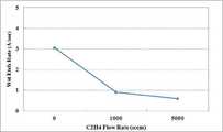
도 7은 에틸 계열의 가스의 공급량과 증착된 박막의 식각률의 관계를 나타내는 그래프이다.
도 8은 본 발명의 일 실시예에 따른 반도체 제조장치를 개략적으로 나타내는 도면이다.
도 9는 본 발명의 다른 실시예에 따른 메모리 소자 제조장치를 개략적으로 나타내는 도면이다.
도 10은 도 9에 도시한 에지링을 개략적으로 나타내는 사시도이다.
도 11 및 도 12는 도 9에 도시한 에지링의 동작을 나타내는 도면이다.1 to 6 are schematic cross-sectional views illustrating a method of manufacturing a memory device according to an embodiment of the present invention.
7 is a graph showing the relationship between the amount of ethyl-based gas supplied and the etch rate of the deposited thin film.
8 is a schematic view of a semiconductor manufacturing apparatus according to an embodiment of the present invention.
9 is a schematic view of a memory device manufacturing apparatus according to another embodiment of the present invention.
FIG. 10 is a perspective view schematically illustrating the edge ring shown in FIG. 9.
11 and 12 are views showing the operation of the edge ring shown in FIG.
이하, 본 발명의 바람직한 실시예들을 첨부된 도 1 내지 도 12를 참고하여 더욱 상세히 설명한다. 본 발명의 실시예들은 여러 가지 형태로 변형될 수 있으며, 본 발명의 범위가 아래에서 설명하는 실시예들에 한정되는 것으로 해석되어서는 안 된다. 본 실시예들은 당해 발명이 속하는 기술분야에서 통상의 지식을 가진 자에게 본 발명을 더욱 상세하게 설명하기 위해서 제공되는 것이다. 따라서 도면에 나타난 각 요소의 형상은 보다 분명한 설명을 강조하기 위하여 과장될 수 있다.
Hereinafter, preferred embodiments of the present invention will be described in more detail with reference to FIGS. 1 to 12. The embodiments of the present invention can be modified in various forms, and the scope of the present invention should not be construed as being limited to the embodiments described below. The embodiments are provided to explain the present invention to a person having ordinary skill in the art to which the present invention belongs. Accordingly, the shape of each element shown in the drawings may be exaggerated to emphasize a clearer description.
도 1 내지 도 6은 본 발명의 일 실시예에 따른 메모리 소자의 제조방법을 보여주는 개략적인 단면도이다. 이하 도 1 내지 도 6을 참고하여 메모리 소자의 제조방법을 설명하기로 한다.
1 to 6 are schematic cross-sectional views illustrating a method of manufacturing a memory device according to an embodiment of the present invention. Hereinafter, a method of manufacturing a memory device will be described with reference to FIGS. 1 to 6.
먼저, 도 1에 도시한 바와 같이, 기판(105)이 제공될 수 있다. 기판(105)은 반도체 물질, 예컨대 Ⅳ족 반도체, Ⅲ-Ⅴ족 화합물 반도체, 또는 Ⅱ-Ⅵ족 산화물 반도체를 포함할 수 있다. 예를 들어, Ⅳ족 반도체는 실리콘, 게르마늄 또는 실리콘-게르마늄을 포함할 수 있다. 기판(105)은 벌크 웨이퍼 또는 에피택셜층으로 제공될 수 있다.
First, as shown in FIG. 1, a
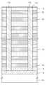
다음으로, 기판(105)의 상부에 불순물들을 주입하여 불순물 영역(110)을 한정할 수 있다. 이어서 기판(105) 상에 절연층들(115) 및 희생층들(120)을 교대로 적층할 수 있다. 절연층들(115)과 희생층들(120)은 8×8이나 18×18, 또는 n×n의 다중층을 이룰 수 있다. 본 실시예에서는 절연층(115)이 먼저 적층되고, 희생층(120)이 나중에 적층되는 것으로 설명하고 있으나, 필요에 따라 절연층(115)과 희생층(120)의 적층 순서는 바뀔 수 있다.
Next, impurities may be implanted in the upper portion of the
절연층(115)은 실리콘산화막(Silicon Dioxide, SiO2)일 수 있으며, 기판(105) 상에 공급된 실란(SiH4)과 산화질소(N2O)를 반응시켜 형성될 수 있다. 실란(SiH4)은 Si2H6, Si3H8, Si4H10 등으로 대체될 수 있다. 마찬가지로, 희생층(120)은 실리콘산화막일 수 있으며, 기판(105) 상에 공급된 디클로로실란(SiCl2H2)(DCS)과 산화질소(N2O)를 반응시켜 형성될 수 있다. 또한, 본 실시예와 달리, 희생층(120)은 기판(105) 상에 SiH4, Si2H6, Si3H8, Si4H10, 디클로로실란(SiCl2H2)을 포함하는 군으로부터 선택된 하나 이상의 가스와 B2H6, PH3를 포함하는 군으로부터 선택된 하나 이상의 가스를 공급하여 형성된 실리콘산화막일 수 있으며, 이 경우, 실리콘 산화막 상에 보론(boron) 또는 인(phosphorus)(보론과 인이 동시에 주입가능)이 주입될 수 있다.
The
다음, 도 2에 도시한 바와 같이, 절연층들(115) 및 희생층들(120)을 식각하여 복수의 관통홀들(125)을 형성할 수 있으며, 관통홀들(125)은 절연층들(115) 및 희생층들(120)을 관통한다. 관통홀들(125)은 공지된 포토리소그래피 및 식각 기술을 이용하여 형성할 수 있다. 이어서, 이미 공지된 반도체 트랜지스터를 형성하기 위한 채널 형성 공정(또는 폴리실리콘 박막을 형성하는 공정)을 통해 관통홀들(125)을 채우도록 패턴들(130)을 형성할 수 있다. 이때, 패턴들(130)은 속이 비어 있는 원통 형상일 수 있으며, 마찬가지로, 패턴들(130)은 절연층들(115) 및 희생층들(120)을 관통한다. 예를 들어, 패턴들(130)은 다결정 구조로 형성하거나 또는 단결정 구조의 에피택셜층과 같은 박막 형상일 수도 있다.
Next, as illustrated in FIG. 2, the plurality of through
다음, 도 3에 도시한 바와 같이, 패턴들(130) 사이의 절연층들(115) 및 희생층들(120)을 식각하여 개구들(135)을 형성할 수 있다. 개구들(135)은 포토리소그래피 및 식각 기술을 이용하여 형성할 수 있다.
Next, as shown in FIG. 3, the
다음, 도 4에 도시한 바와 같이, 희생층들(120)을 제거할 수 있다. 앞서 설명한 바와 같이, 절연층(115)은 실란에 의해 형성된 실리콘산화막이며, 희생층(120)은 디클로로실란에 의해 형성된 실리콘산화막이거나 SiH4, Si2H6, Si3H8, Si4H10, 디클로로실란(SiCl2H2)을 포함하는 군으로부터 선택된 하나 이상의 가스와 B2H6, PH3를 포함하는 군으로부터 선택된 하나 이상의 가스를 공급하여 형성되어 보론(boron) 또는 인(phosphorus)(보론과 인이 동시에 주입가능)이 주입된 실리콘산화막일 수 있다. 아래는 실란에 의해 형성된 실리콘산화막과 디클로로실란에 의해 형성된 실리콘산화막이 가지는 특성을 나타낸다.
Next, as shown in FIG. 4, the
E/R(HF)
100:1
(A/sec)(As Dep)
E / R (HF)
100: 1
(A / sec)
위 표에 나타낸 바와 같이, 희생층(120)은 절연층(115)에 대해서 식각 선택비(etch selectivity)를 가지며, 희생층(120)의 식각률은 절연층(115)의 식각률에 비해 20배 가량의 크기를 가진다. 따라서, 절연층(115)과 희생층(120)이 동일한 시간 동안 에천트에 노출되었을 때, 식각된 희생층(120)의 크기는 식각된 절연층(115)의 크기에 20배 이상이며, 절연층(115)의 식각된 정도는 매우 작다. 디클로로실란에 의해 형성된 실리콘산화막과 같이 Cl기를 가지는 실리콘산화막은 증착 박막의 밀도가 상대적으로 낮아 높은 식각률을 나타낸다.
As shown in the above table, the
위와 같은 원리를 이용하여 희생층(120)을 제거할 수 있다. 등방성 식각을 이용하여 에천트를 개구들(135)로부터 절연층들(115) 사이로 침투시킬 수 있으며, 등방성 식각은 습식 식각 또는 화학적 건식 식각(chemical dry etch)을 포함할 수 있다. 에천트는 HF 또는 BOE(buffered oxide etch) 중 어느 하나를 포함할 수 있다. 이에 따라, 절연층들(115) 사이의 희생층들(120)이 제거되어 개구들(135)과 연결된 터널들(140)이 형성될 수 있다. 터널들(140)에 의해서 패턴들(130)의 측벽들이 노출될 수 있다.
The
다음, 도 5에 도시한 바와 같이, 개구들(도 8의 135) 및 터널들(도 8의 140)에 의해서 노출된 절연층들(115) 및 패턴들(130)의 측벽들 상에 스토리지 매체들(150)을 형성할 수 있다. 스토리지 매체들(150)은 터널링 절연층(142), 전하 저장층(144) 및 블로킹 절연층(146)을 순차로 형성할 수 있다. 이어서 스토리지 매체들(150) 상에 도전층(155)을 형성할 수 있다. 예를 들어, 스토리지 매체들(150) 및 도전층(155)은 모서리 도포성이 높은 화학기상증착 또는 도금법을 이용하여 형성할 수 있다.
Next, as shown in FIG. 5, the storage medium on the sidewalls of the insulating
다음, 도 6에 도시한 바와 같이, 개구들(도 4의 135)에 의해서 노출된 도전층(도 5의 155)을 선택적으로 식각하여 접지 선택 게이트 전극들(162), 제어 게이트 전극들(164) 및 스트링 선택 게이트 전극들(166)을 형성할 수 있다.
Next, as illustrated in FIG. 6, the conductive layer exposed by the
한편, 본 실시예와 달리, 에틸계열의 가스(예를 들어, C2H4) 또는 메틸계열의 가스(예를 들어, CH3)가 실란(SiH4)과 함께 공급될 수 있으며, 이로 인해 절연층(115)은 SiCO(Silicon Carbon Oxide) 박막일 수 있다. SiCO 박막으로 이루어진 절연층(115)은 앞서 설명한 디클로로실란에 의해 형성된 희생층(120)에 비해 더욱 큰 식각 선택비를 가지므로, 희생층(120)의 제거시 함께 손상되는 절연층(115)의 양을 최소화할 수 있다. 도 7은 에틸 계열의 가스의 공급량과 증착된 박막의 식각률의 관계를 나타내는 그래프이다. 도 7에 도시한 바와 같이, 에틸 계열의 가스가 공급됨에 따라, 증착된 박막의 식각률은 감소하는 것을 알 수 있으며, 이를 통해 희생층(120)과의 식각 선택비를 요구에 따라 조절할 수 있다.
On the other hand, unlike the present embodiment, an ethyl series gas (eg, C2 H4 ) or a methyl series gas (eg, CH3 ) may be supplied together with the silane (SiH4 ). The insulating
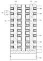
도 8은 본 발명의 일 실시예에 따른 반도체 제조장치를 개략적으로 나타내는 도면이다. 도 8에 도시한 바와 같이, 반도체 제조장치(10)는 소스가스 또는 반응가스가 도입되기 위한 도입부(12)를 가지며, 소스가스 또는 반응가스는 도입부(12)를 통해 도입되며, 샤워헤드(13)를 통해 챔버(11)의 내부에 분사된다. 공정진행시 실란 또는 디클로로실란은 1-1000 sccm 공급될 수 있으며, 반응가스(예를 들어, N2O)는 100-50000 sccm 공급될 수 있다. 한편, 앞서 설명한 바와 같이, 에틸계열의 가스(예를 들어, C2H4) 또는 메틸계열의 가스(예를 들어, CH3)가 공급될 경우, 50 내지 10000 sccm 공급될 수 있다.8 is a schematic view of a semiconductor manufacturing apparatus according to an embodiment of the present invention. As shown in FIG. 8, the
공정의 대상이 되는 기판(100)은 히터(14)의 상부에 놓여지며, 히터(14)는 히터지지대(16)에 의해 지지된다. 히터(14)는 공정진행 중 기판의 온도를 300 내지 790도로 유지할 수 있으며, 이때 챔버(11) 내부의 압력은 10 mTorr 내지 250 Torr를 유지할 수 있다. 공정이 완료된 기판(100)은 배출부(17)를 통해 외부로 배출된다.
The
도 9는 본 발명의 다른 실시예에 따른 메모리 소자 제조장치를 개략적으로 나타내는 도면이며, 도 10은 도 9에 도시한 에지링을 개략적으로 나타내는 사시도이다. 이하에서는 도 8과 구별되는 부분에 대해서만 설명하기로 하며, 생략된 설명은 도 8에 대한 설명으로 대체될 수 있다.
FIG. 9 is a schematic view of a memory device manufacturing apparatus according to another exemplary embodiment of the present invention, and FIG. 10 is a perspective view schematically illustrating the edge ring shown in FIG. 9. Hereinafter, only portions distinguished from FIG. 8 will be described, and a description omitted may be replaced with the description of FIG. 8.
도 9에 도시한 바와 같이, 메모리 소자 제조장치(210)는 챔버(211)의 내부에 설치된 기판지지대(214)를 구비하며, 기판지지대(214)는 지지대(216)에 의해 지지된다. 후술하는 바와 같이, 기판지지대(214)는 별도의 구동부(도시안함)에 의해 지지대(216)와 함께 승강하며, 이로 인해, 기판(215)이 챔버(211)의 내부를 출입할 수 있는 해제위치(도 9에 도시)와 기판(215)에 대한 공정이 이루어지는 공정위치(도 11에 도시)로 전환된다.
As shown in FIG. 9, the memory
기판(215)은 챔버(211)의 측벽에 형성된 배출부(217)를 통해 챔버(211)의 내부를 출입하며, 배출부(217)를 통해 챔버(211)의 내부로 이동한 기판(215)은 기판지지대(214)의 상부에 위치한다. 기판지지대(214)는 기판(215)에 비해 큰 직경을 가지며, 기판(215)은 기판지지대(214)의 중앙에 위치한다. 이때, 기판(215)은 기판지지대(214)를 관통하는 리프트핀(220)에 의해 지지되며, 기판지지대(214)로부터 상승이격된 상태를 유지한다. 또한, 샤워헤드(213)는 기판지지대(214)의 상부에 설치되며, 소스가스 또는 반응가스는 샤워헤드(213)를 통해 챔버(211)의 내부에 분사된다.
The
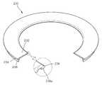
한편, 챔버(211)는 베큠 가이드(vacuum guide)(212) 및 에지링(230)을 더 포함한다. 베큠 가이드(212)는 원통 형상으로 챔버(211)의 내부에 설치된다. 도 10에 도시한 바와 같이, 에지링(230)은 챔버(211)의 내부형상과 대응되는 링 형상이며, 에지링(230)은 지지부(232), 수평지지부(234), 수직지지부(236), 그리고 가압면(238a)을 가지는 가압부(238)를 구비한다. 에지링(230)은 기판지지대(214)와 샤워헤드(213) 사이에 위치하여 베큠 가이드(212)의 내측벽으로부터 돌출된 고정돌기(212a) 상에 놓여진다. 도 9에 도시한 바와 같이, 기판지지대(214)가 해제위치에 위치할 때 에지링(230)은 고정돌기(212a) 상에 위치하며, 후술하는 바와 같이, 기판지지대(214)가 공정위치로 전환될 때 에지링(230)은 고정돌기(212a)로부터 이탈하여 기판지지대(214)의 상부에 놓여진다.
Meanwhile, the
도 11 및 도 12는 도 9에 도시한 에지링의 동작을 나타내는 도면이다. 앞서 설명한 바와 같이, 기판지지대(214)는 구동부(도시안함)에 의해 지지대(216)와 함께 승강하며, 이로 인해, 해제위치 및 공정위치로 전환될 수 있다.
11 and 12 are views showing the operation of the edge ring shown in FIG. As described above, the
도 12에 도시한 바와 같이, 수평지지부(234)는 지지부(232)로부터 챔버(211)의 측벽을 향해 연장되며, 수직지지부(236)는 지지부(232)로부터 하부를 향해 연장된다. 가압부(238)는 지지부(232)로부터 챔버(211)의 내측을 향해 하향경사지도록 연장된다.
As shown in FIG. 12, the
도 9에 도시한 바와 같이, 기판지지대(214)가 해제위치에 있을 때, 에지링(230)은 수평지지부(234) 및 수직지지부(236)에 의해 고정돌기(212a) 상에 위치할 수 있으며, 수평지지부(234)는 고정돌기(212a)의 상면과 접하고 수직지지부(236)는 고정돌기(212a)의 측면과 접한다. 이때, 지지부(232) 및 가압부(238)는 챔버(211)의 내측을 향해 돌출된 상태를 유지한다.
As shown in FIG. 9, when the
도 11에 도시한 바와 같이, 기판지지대(214)가 공정위치로 전환될 때, 기판지지대(214)는 기판(215)의 외측에 위치하는 링 형상의 에지부를 이용하여 에지링(230)을 들어 올리게 되며, 이로 인해, 에지링(230)은 고정돌기(212a)로부터 이탈되어 상승한다. 이때, 도 12에 도시한 바와 같이, 지지부(232)는 기판지지대(214)의 에지부와 인접하며, 가압부(238)는 기판지지대(214)에 놓여진 기판(215)의 에지부와 접촉하여 기판(215)의 에지부를 가압한다. 즉, 에지링(230)은 기판지지대(214)에 놓여진 상태에서 자중에 의해 기판(215)의 에지부를 가압하며, 가압부(238)는 기판(215)의 에지부와 접촉하는 가압면(238a)을 가진다.
As shown in FIG. 11, when the
앞서 도 1을 통해 설명한 바와 같이, 기판 상에 서로 다른 실리콘 산화막을 교대로 적층할 경우, 공정으로 인해 두 개의 실리콘 산화막 사이에 응력의 차이가 발생하며, 이로 인해, 기판의 변형(warpage, 휨 또는 뒤틀림)이 발생한다. 이와 같은 기판의 변형으로 인해 기판의 에지부는 기판지지대로부터 이격되며, 기판은 기판의 센터부가 오목한 'U'자 형상으로 변형된다. 이는 기판 내의 온도분포(기판의 센터와 에지 사이에) 등에 영향을 미치므로, 공정균일도(예를 들어, 증착률)에 큰 영향을 미친다. 실제, 위와 같은 공정을 마친 이후, 기판의 에지부에서 측정된 증착률이 기판의 센터부에서 측정된 증착률에 비해 현저히 낮음을 알 수 있었다. 따라서, 기판의 에지부가 기판지지대로부터 이격되어 기판이 변형되는 현상을 방지하기 위하여 에지링(230)의 가압부(238)를 이용하여 기판(215)의 에지부를 가압할 수 있다.
As described above with reference to FIG. 1, when alternately stacking different silicon oxide films on a substrate, a difference in stress occurs between two silicon oxide films due to a process, and thus, warpage, warpage or Distortion) occurs. Due to the deformation of the substrate, the edge portion of the substrate is spaced apart from the substrate support, and the substrate is deformed into a 'U' shape in which the center portion of the substrate is concave. This affects the temperature distribution in the substrate (between the center and the edge of the substrate) and the like, and thus greatly affects the process uniformity (eg, deposition rate). In fact, after the above process, it was found that the deposition rate measured at the edge portion of the substrate is significantly lower than the deposition rate measured at the center portion of the substrate. Accordingly, the edge portion of the
한편, 도 12에 도시한 바와 같이, 에지링(230)의 가압부(238)에 의해 가압되는 기판(215)의 에지부의 폭(w)은 기판(215)의 에지로부터 0.5 ㎜ 내지 3 ㎜ 가량내측일 수 있으며, 이 부분은 실제 반도체 공정에서 반도체 소자로 사용하지 않는 부분이므로, 반도체 소자의 수율에 영향을 미치지 않는다. 또한, 앞서 설명한 가압면(238a)은 에지부와 대응되는 폭(w)을 가질 수 있다.
Meanwhile, as shown in FIG. 12, the width w of the edge portion of the
도 12에 도시한 바와 같이, 에지링(230)은 가압부(238)만으로 기판지지대(214) 상에 지지된 상태를 유지할 수 있으며, 지지부(232)는 기판지지대(214)의 에지부로부터 이격된 상태(d)를 유지할 수 있다. 이 경우, 에지링(230)의 전체 무게가 가압부(238)의 가압면(238a)을 통해 기판(215)의 에지부에 전달되므로, 에지링(230)의 무게를 최소화하고도 높은 압력을 기판(215)의 에지부에 전달할 수 있다. 이와 같은 원리는 압력의 크기가 접촉면적의 크기에 반비례한다는 사실로부터 이해될 수 있다.
As shown in FIG. 12, the
본 발명을 바람직한 실시예들을 통하여 상세하게 설명하였으나, 이와 다른 형태의 실시예들도 가능하다. 그러므로, 이하에 기재된 청구항들의 기술적 사상과 범위는 바람직한 실시예들에 한정되지 않는다.Although the present invention has been described in detail by way of preferred embodiments thereof, other forms of embodiment are possible. Therefore, the technical idea and scope of the claims set forth below are not limited to the preferred embodiments.
105 : 기판
115 : 절연층
120 : 희생층
130 : 패턴105: substrate
115: insulation layer
120: sacrificial layer
130: pattern
Claims (14)
Translated fromKorean기판 상에 하나 이상의 절연층 및 하나 이상의 희생층을 교대로 적층하는 단계;
상기 절연층 및 상기 희생층을 관통하는 관통홀을 형성하는 단계;
상기 관통홀을 채우는 패턴을 형성하는 단계;
상기 절연층 및 상기 희생층을 관통하는 개구를 형성하는 단계; 및
상기 개구를 통해 에천트를 공급하여 상기 희생층을 제거하는 단계를 포함하되,
상기 절연층을 적층하는 단계는 상기 기판에 SiH4, Si2H6, Si3H8, Si4H10을 포함하는 군으로부터 선택된 하나 이상의 가스를 공급하여 제1 실리콘 산화막을 증착하는 단계를 포함하고,
상기 희생층을 적층하는 단계는 상기 기판에 디클로로실란(SiCl2H2)을 공급하여 제2 실리콘 산화막을 증착하는 단계를 포함하며,
상기 절연층의 상기 제1 실리콘 산화막 및 상기 희생층의 상기 제2 실리콘 산화막은 상기 에천트에 대해 식각 선택비(etch selectivity)를 갖는 것을 특징으로 하는 3차원 구조의 메모리 소자를 제조하는 방법.In the method of manufacturing a three-dimensional memory device,
Alternately stacking one or more insulating layers and one or more sacrificial layers on the substrate;
Forming a through hole penetrating the insulating layer and the sacrificial layer;
Forming a pattern filling the through hole;
Forming an opening penetrating the insulating layer and the sacrificial layer; And
Supplying an etchant through the opening to remove the sacrificial layer,
The stacking of the insulating layer may include depositing a first silicon oxide layer by supplying at least one gas selected from the group including SiH4 , Si2 H6 , Si3 H8 , and Si4 H10 to the substrate. and,
The stacking of the sacrificial layer includes supplying dichlorosilane (SiCl2 H2 ) to the substrate and depositing a second silicon oxide layer.
The first silicon oxide film of the insulating layer and the second silicon oxide film of the sacrificial layer have an etch selectivity with respect to the etchant.
기판 상에 하나 이상의 절연층 및 하나 이상의 희생층을 교대로 적층하는 단계;
상기 절연층 및 상기 희생층을 관통하는 관통홀을 형성하는 단계;
상기 관통홀을 채우는 패턴을 형성하는 단계;
상기 절연층 및 상기 희생층을 관통하는 개구를 형성하는 단계; 및
상기 개구를 통해 에천트를 공급하여 상기 희생층을 제거하는 단계를 포함하되,
상기 절연층을 적층하는 단계는 상기 기판에 SiH4, Si2H6, Si3H8, Si4H10을 포함하는 군으로부터 선택된 하나 이상의 가스와 에틸계열의 가스를 공급하여 제1 실리콘 산화막을 증착하는 단계를 포함하고,
상기 희생층을 적층하는 단계는 상기 기판에 디클로로실란(SiCl2H2)을 공급하여 제2 실리콘 산화막을 증착하는 단계를 포함하며,
상기 제1 실리콘 산화막은 SiCO(Silicon Carbon Oxide)이고,
상기 절연층의 상기 제1 실리콘 산화막 및 상기 희생층의 상기 제2 실리콘 산화막은 상기 에천트에 대해 식각 선택비를 갖는 것을 특징으로 하는 3차원 구조의 메모리 소자를 제조하는 방법.In the method of manufacturing a three-dimensional memory device,
Alternately stacking one or more insulating layers and one or more sacrificial layers on the substrate;
Forming a through hole penetrating the insulating layer and the sacrificial layer;
Forming a pattern filling the through hole;
Forming an opening penetrating the insulating layer and the sacrificial layer; And
Supplying an etchant through the opening to remove the sacrificial layer,
The stacking of the insulating layer may include supplying at least one gas selected from a group including SiH4 , Si2 H6 , Si3 H8 , and Si4 H10 and an ethyl series gas to the substrate to form a first silicon oxide film. Including depositing,
The stacking of the sacrificial layer includes supplying dichlorosilane (SiCl2 H2 ) to the substrate and depositing a second silicon oxide layer.
The first silicon oxide film is silicon carbon oxide (SiCO),
And wherein the first silicon oxide film of the insulating layer and the second silicon oxide film of the sacrificial layer have an etch selectivity with respect to the etchant.
기판 상에 하나 이상의 절연층 및 하나 이상의 희생층을 교대로 적층하는 단계;
상기 절연층 및 상기 희생층을 관통하는 관통홀을 형성하는 단계;
상기 관통홀을 채우는 패턴을 형성하는 단계;
상기 절연층 및 상기 희생층을 관통하는 개구를 형성하는 단계; 및
상기 개구를 통해 에천트를 공급하여 상기 희생층을 제거하는 단계를 포함하되,
상기 절연층을 적층하는 단계는 상기 기판에 SiH4, Si2H6, Si3H8, Si4H10을 포함하는 군으로부터 선택된 하나 이상의 가스와 메틸계열의 가스를 공급하여 제1 실리콘 산화막을 증착하는 단계를 포함하고,
상기 희생층을 적층하는 단계는 상기 기판에 디클로로실란(SiCl2H2)을 공급하여 제2 실리콘 산화막을 증착하는 단계를 포함하며,
상기 제1 실리콘 산화막은 SiCO(Silicon Carbon Oxide)이고,
상기 절연층의 상기 제1 실리콘 산화막 및 상기 희생층의 상기 제2 실리콘 산화막은 상기 에천트에 대해 식각 선택비를 갖는 것을 특징으로 하는 3차원 구조의 메모리 소자를 제조하는 방법.In the method of manufacturing a three-dimensional memory device,
Alternately stacking one or more insulating layers and one or more sacrificial layers on the substrate;
Forming a through hole penetrating the insulating layer and the sacrificial layer;
Forming a pattern filling the through hole;
Forming an opening penetrating the insulating layer and the sacrificial layer; And
Supplying an etchant through the opening to remove the sacrificial layer,
The stacking of the insulating layer may include supplying at least one gas selected from a group including SiH4 , Si2 H6 , Si3 H8 , and Si4 H10 and a methyl-based gas to the substrate to form a first silicon oxide film. Including depositing,
The stacking of the sacrificial layer includes supplying dichlorosilane (SiCl2 H2 ) to the substrate and depositing a second silicon oxide layer.
The first silicon oxide film is silicon carbon oxide (SiCO),
And wherein the first silicon oxide film of the insulating layer and the second silicon oxide film of the sacrificial layer have an etch selectivity with respect to the etchant.
상기 희생층의 식각률은 상기 절연층의 식각률에 비해 5배 내지 300배인 것을 특징으로 하는 3차원 구조의메모리 소자를 제조하는 방법.4. The method according to any one of claims 1 to 3,
The etching rate of the sacrificial layer is a method of manufacturing a memory device having a three-dimensional structure, characterized in that 5 to 300 times the etching rate of the insulating layer.
상기 에천트는 HF 또는 BOE 중 어느 하나를 포함하는 것을 특징으로 하는 3차원 구조의 메모리 소자를 제조하는 방법.4. The method according to any one of claims 1 to 3,
And the etchant comprises one of HF and BOE.
상기 기판의 온도는 300 내지 790도를 유지하며,
상기 기판의 공정압력은 10 mTorr 내지 250 Torr를 유지하는 것을 특징으로 하는 3차원 구조의 메모리 소자를 제조하는 방법.4. The method according to any one of claims 1 to 3,
The temperature of the substrate is maintained at 300 to 790 degrees,
The process pressure of the substrate is a method of manufacturing a memory device having a three-dimensional structure, characterized in that to maintain a 10 mTorr to 250 Torr.
상기 제1 실리콘 산화막과 상기 제2 실리콘 산화막은 서로 다른 두께를 가지는 것을 특징으로 하는 3차원 구조의 메모리 소자를 제조하는 방법.4. The method according to any one of claims 1 to 3,
And the first silicon oxide film and the second silicon oxide film have different thicknesses.
상기 절연층 및 희생층을 교대로 적층하는 단계는 에지링을 이용하여 상기 기판의 에지부를 가압하는 단계를 더 포함하는 것을 특징으로 하는 3차원 구조의 메모리 소자를 제조하는 방법.4. The method according to any one of claims 1 to 3,
Alternately stacking the insulating layer and the sacrificial layer further comprises pressing an edge portion of the substrate by using an edge ring.
상기 기판의 에지부는 상기 기판의 에지로부터 0.5 ㎜ 내지 3 ㎜ 내측에 해당하는 것을 특징으로 하는 3차원 구조의 메모리 소자를 제조하는 방법.9. The method of claim 8,
And an edge portion of the substrate corresponds to an inner side of 0.5 mm to 3 mm from an edge of the substrate.
상기 에지링은 세라믹 재질인 것을 특징으로 하는 3차원 구조의 메모리 소자를 제조하는 방법.9. The method of claim 8,
The edge ring is a method of manufacturing a memory device having a three-dimensional structure, characterized in that the ceramic material.
기판 상에 하나 이상의 절연층 및 하나 이상의 희생층을 교대로 적층하는 단계;
상기 절연층 및 상기 희생층을 관통하는 관통홀을 형성하는 단계;
상기 관통홀을 채우는 패턴을 형성하는 단계;
상기 절연층 및 상기 희생층을 관통하는 개구를 형성하는 단계; 및
상기 개구를 통해 에천트를 공급하여 상기 희생층을 제거하는 단계를 포함하되,
상기 절연층을 적층하는 단계는 상기 기판에 SiH4, Si2H6, Si3H8, Si4H10을 포함하는 군으로부터 선택된 하나 이상의 가스를 공급하여 제1 실리콘 산화막을 증착하는 단계를 포함하고,
상기 희생층을 적층하는 단계는 상기 기판에 SiH4, Si2H6, Si3H8, Si4H10, 디클로로실란(SiCl2H2)을 포함하는 군으로부터 선택된 하나 이상의 가스와 B2H6, PH3를 포함하는 군으로부터 선택된 하나 이상의 가스를 공급하여 보론(boron) 또는 인(phosphorus)이 주입된 제2 실리콘 산화막을 증착하는 단계를 포함하며,
상기 절연층의 상기 제1 실리콘 산화막 및 상기 희생층의 상기 제2 실리콘 산화막은 상기 에천트에 대해 식각 선택비(etch selectivity)를 갖는 것을 특징으로 하는 3차원 구조의 메모리 소자를 제조하는 방법.In the method of manufacturing a three-dimensional memory device,
Alternately stacking one or more insulating layers and one or more sacrificial layers on the substrate;
Forming a through hole penetrating the insulating layer and the sacrificial layer;
Forming a pattern filling the through hole;
Forming an opening penetrating the insulating layer and the sacrificial layer; And
Supplying an etchant through the opening to remove the sacrificial layer,
The stacking of the insulating layer may include depositing a first silicon oxide layer by supplying at least one gas selected from the group including SiH4 , Si2 H6 , Si3 H8 , and Si4 H10 to the substrate. and,
The stacking of the sacrificial layer may include one or more gases selected from the group including SiH4 , Si2 H6 , Si3 H8 , Si4 H10 , and dichlorosilane (SiCl2 H2 ), and B2 H on the substrate.6 , supplying at least one gas selected from the group comprising PH3 to deposit a second silicon oxide film in which boron or phosphorus is implanted,
The first silicon oxide film of the insulating layer and the second silicon oxide film of the sacrificial layer have an etch selectivity with respect to the etchant.
기판에 대한 공정이 이루어지는 챔버;
상기 챔버 내에 설치되어 상기 기판이 놓여지는 기판지지대; 및
상기 기판 상에 상기 절연층을 적층할 때 상기 기판에 SiH4, Si2H6, Si3H8, Si4H10을 포함하는 군으로부터 선택된 하나 이상의 가스를 공급하고, 상기 기판 상에 상기 희생층을 적층할 때 상기 기판에 디클로로실란(SiCl2H2)을 공급하는 샤워헤드를 포함하며,
상기 절연층 및 상기 희생층은 에천트에 대해 식각 선택비(etch selectivity)를 갖는 것을 특징으로 하는 3차원 구조의 메모리 소자 제조장치.An apparatus for manufacturing a memory device having a three-dimensional structure by alternately stacking at least one insulating layer and at least one sacrificial layer on a substrate,
A chamber in which a process is performed on the substrate;
A substrate support installed in the chamber and on which the substrate is placed; And
When stacking the insulating layer on the substrate, at least one gas selected from the group comprising SiH4 , Si2 H6 , Si3 H8 , Si4 H10 is supplied to the substrate, and the sacrificial material on the substrate A showerhead supplying dichlorosilane (SiCl2 H2 ) to the substrate when the layers are stacked,
And the insulating layer and the sacrificial layer have an etch selectivity with respect to the etchant.
기판에 대한 공정이 이루어지는 챔버;
상기 챔버 내에 설치되어 상기 기판이 놓여지는 기판지지대; 및
상기 기판 상에 상기 절연층을 적층할 때 상기 기판에 SiH4, Si2H6, Si3H8, Si4H10을 포함하는 군으로부터 선택된 하나 이상의 가스를 공급하고, 상기 기판 상에 상기 희생층을 적층할 때 상기 기판에 SiH4, Si2H6, Si3H8, Si4H10, 디클로로실란(SiCl2H2)을 포함하는 군으로부터 선택된 하나 이상의 가스와 B2H6, PH3를 포함하는 군으로부터 선택된 하나 이상의 가스를 공급하는 샤워헤드를 포함하며,
상기 절연층 및 상기 희생층은 에천트에 대해 식각 선택비(etch selectivity)를 갖는 것을 특징으로 하는 3차원 구조의 메모리 소자 제조장치.An apparatus for manufacturing a memory device having a three-dimensional structure by alternately stacking at least one insulating layer and at least one sacrificial layer on a substrate,
A chamber in which a process is performed on the substrate;
A substrate support installed in the chamber and on which the substrate is placed; And
When stacking the insulating layer on the substrate, at least one gas selected from the group comprising SiH4 , Si2 H6 , Si3 H8 , Si4 H10 is supplied to the substrate, and the sacrificial material on the substrate At least one gas selected from the group comprising SiH4 , Si2 H6 , Si3 H8 , Si4 H10 , dichlorosilane (SiCl2 H2 ), B2 H6 , PH A showerhead for supplying one or more gases selected from the group comprising3 ,
And the insulating layer and the sacrificial layer have an etch selectivity with respect to the etchant.
상기 샤워헤드는, 상기 절연층을 적층할 때 상기 기판에 에틸계열의 가스 또는 메틸계열의 가스를 더 공급하는 것을 특징으로 하는 3차원 구조의 메모리 소자 제조장치.
The method according to claim 12 or 13,
The shower head is a three-dimensional memory device manufacturing apparatus, characterized in that for supplying the ethyl-based gas or methyl-based gas to the substrate when the insulating layer is laminated.
Priority Applications (5)
| Application Number | Priority Date | Filing Date | Title |
|---|---|---|---|
| KR1020100100092AKR101209003B1 (en) | 2010-10-14 | 2010-10-14 | Method and apparatus for manufacturing memory device having 3 dimensional structure |
| CN201180048997.2ACN103155139B (en) | 2010-10-14 | 2011-10-06 | Method and device for manufacturing three-dimensional structure memory element |
| US13/822,416US9425057B2 (en) | 2010-10-14 | 2011-10-06 | Method and apparatus for manufacturing three-dimensional-structure memory device |
| JP2013531511AJP5705990B2 (en) | 2010-10-14 | 2011-10-06 | Method for manufacturing a memory element having a three-dimensional structure |
| PCT/KR2011/007402WO2012050321A2 (en) | 2010-10-14 | 2011-10-06 | Method and apparatus for manufacturing three-dimensional- structure memory device |
Applications Claiming Priority (1)
| Application Number | Priority Date | Filing Date | Title |
|---|---|---|---|
| KR1020100100092AKR101209003B1 (en) | 2010-10-14 | 2010-10-14 | Method and apparatus for manufacturing memory device having 3 dimensional structure |
Publications (2)
| Publication Number | Publication Date |
|---|---|
| KR20120038577A KR20120038577A (en) | 2012-04-24 |
| KR101209003B1true KR101209003B1 (en) | 2012-12-06 |
Family
ID=45938774
Family Applications (1)
| Application Number | Title | Priority Date | Filing Date |
|---|---|---|---|
| KR1020100100092AActiveKR101209003B1 (en) | 2010-10-14 | 2010-10-14 | Method and apparatus for manufacturing memory device having 3 dimensional structure |
Country Status (5)
| Country | Link |
|---|---|
| US (1) | US9425057B2 (en) |
| JP (1) | JP5705990B2 (en) |
| KR (1) | KR101209003B1 (en) |
| CN (1) | CN103155139B (en) |
| WO (1) | WO2012050321A2 (en) |
Families Citing this family (96)
| Publication number | Priority date | Publication date | Assignee | Title |
|---|---|---|---|---|
| US10283321B2 (en) | 2011-01-18 | 2019-05-07 | Applied Materials, Inc. | Semiconductor processing system and methods using capacitively coupled plasma |
| US9064815B2 (en) | 2011-03-14 | 2015-06-23 | Applied Materials, Inc. | Methods for etch of metal and metal-oxide films |
| US9267739B2 (en) | 2012-07-18 | 2016-02-23 | Applied Materials, Inc. | Pedestal with multi-zone temperature control and multiple purge capabilities |
| US9373517B2 (en) | 2012-08-02 | 2016-06-21 | Applied Materials, Inc. | Semiconductor processing with DC assisted RF power for improved control |
| US9034770B2 (en) | 2012-09-17 | 2015-05-19 | Applied Materials, Inc. | Differential silicon oxide etch |
| US9132436B2 (en) | 2012-09-21 | 2015-09-15 | Applied Materials, Inc. | Chemical control features in wafer process equipment |
| TW201413780A (en)* | 2012-09-24 | 2014-04-01 | Eugene Technology Co Ltd | Apparatus for removing fume and apparatus for processing substrate |
| US10256079B2 (en) | 2013-02-08 | 2019-04-09 | Applied Materials, Inc. | Semiconductor processing systems having multiple plasma configurations |
| US9362130B2 (en) | 2013-03-01 | 2016-06-07 | Applied Materials, Inc. | Enhanced etching processes using remote plasma sources |
| KR101603971B1 (en)* | 2014-07-30 | 2016-03-17 | 피에스케이 주식회사 | Substrate treating apparatus and Substrate treating method |
| CN105448924B (en)* | 2014-08-28 | 2018-08-10 | 旺宏电子股份有限公司 | Three-dimensional memory device with low dielectric constant insulating material and manufacturing method thereof |
| JP6347548B2 (en) | 2014-09-08 | 2018-06-27 | 株式会社日立国際電気 | Semiconductor device manufacturing method, substrate processing apparatus, and program |
| US9355922B2 (en) | 2014-10-14 | 2016-05-31 | Applied Materials, Inc. | Systems and methods for internal surface conditioning in plasma processing equipment |
| US9966240B2 (en) | 2014-10-14 | 2018-05-08 | Applied Materials, Inc. | Systems and methods for internal surface conditioning assessment in plasma processing equipment |
| US11637002B2 (en) | 2014-11-26 | 2023-04-25 | Applied Materials, Inc. | Methods and systems to enhance process uniformity |
| US10224210B2 (en) | 2014-12-09 | 2019-03-05 | Applied Materials, Inc. | Plasma processing system with direct outlet toroidal plasma source |
| US10573496B2 (en) | 2014-12-09 | 2020-02-25 | Applied Materials, Inc. | Direct outlet toroidal plasma source |
| US11257693B2 (en) | 2015-01-09 | 2022-02-22 | Applied Materials, Inc. | Methods and systems to improve pedestal temperature control |
| US9728437B2 (en) | 2015-02-03 | 2017-08-08 | Applied Materials, Inc. | High temperature chuck for plasma processing systems |
| US20160225652A1 (en) | 2015-02-03 | 2016-08-04 | Applied Materials, Inc. | Low temperature chuck for plasma processing systems |
| US9881805B2 (en) | 2015-03-02 | 2018-01-30 | Applied Materials, Inc. | Silicon selective removal |
| DE102015208852A1 (en)* | 2015-05-13 | 2016-11-17 | Nanoscribe Gmbh | Method for producing a three-dimensional structure |
| US9691645B2 (en) | 2015-08-06 | 2017-06-27 | Applied Materials, Inc. | Bolted wafer chuck thermal management systems and methods for wafer processing systems |
| US9741593B2 (en) | 2015-08-06 | 2017-08-22 | Applied Materials, Inc. | Thermal management systems and methods for wafer processing systems |
| US9349605B1 (en) | 2015-08-07 | 2016-05-24 | Applied Materials, Inc. | Oxide etch selectivity systems and methods |
| US10504700B2 (en) | 2015-08-27 | 2019-12-10 | Applied Materials, Inc. | Plasma etching systems and methods with secondary plasma injection |
| JP6479698B2 (en)* | 2016-02-18 | 2019-03-06 | 東芝メモリ株式会社 | Semiconductor manufacturing apparatus and semiconductor device manufacturing method |
| US10522371B2 (en) | 2016-05-19 | 2019-12-31 | Applied Materials, Inc. | Systems and methods for improved semiconductor etching and component protection |
| US10504754B2 (en) | 2016-05-19 | 2019-12-10 | Applied Materials, Inc. | Systems and methods for improved semiconductor etching and component protection |
| US9865484B1 (en) | 2016-06-29 | 2018-01-09 | Applied Materials, Inc. | Selective etch using material modification and RF pulsing |
| JP6419762B2 (en)* | 2016-09-06 | 2018-11-07 | 株式会社Kokusai Electric | Semiconductor device manufacturing method, substrate processing apparatus, and program |
| US10062575B2 (en) | 2016-09-09 | 2018-08-28 | Applied Materials, Inc. | Poly directional etch by oxidation |
| US10629473B2 (en) | 2016-09-09 | 2020-04-21 | Applied Materials, Inc. | Footing removal for nitride spacer |
| US10062585B2 (en) | 2016-10-04 | 2018-08-28 | Applied Materials, Inc. | Oxygen compatible plasma source |
| US9934942B1 (en) | 2016-10-04 | 2018-04-03 | Applied Materials, Inc. | Chamber with flow-through source |
| US10546729B2 (en) | 2016-10-04 | 2020-01-28 | Applied Materials, Inc. | Dual-channel showerhead with improved profile |
| US10062579B2 (en) | 2016-10-07 | 2018-08-28 | Applied Materials, Inc. | Selective SiN lateral recess |
| US9947549B1 (en) | 2016-10-10 | 2018-04-17 | Applied Materials, Inc. | Cobalt-containing material removal |
| US10163696B2 (en) | 2016-11-11 | 2018-12-25 | Applied Materials, Inc. | Selective cobalt removal for bottom up gapfill |
| US9768034B1 (en) | 2016-11-11 | 2017-09-19 | Applied Materials, Inc. | Removal methods for high aspect ratio structures |
| US10242908B2 (en) | 2016-11-14 | 2019-03-26 | Applied Materials, Inc. | Airgap formation with damage-free copper |
| US10026621B2 (en) | 2016-11-14 | 2018-07-17 | Applied Materials, Inc. | SiN spacer profile patterning |
| US10566206B2 (en) | 2016-12-27 | 2020-02-18 | Applied Materials, Inc. | Systems and methods for anisotropic material breakthrough |
| US10403507B2 (en) | 2017-02-03 | 2019-09-03 | Applied Materials, Inc. | Shaped etch profile with oxidation |
| US10431429B2 (en) | 2017-02-03 | 2019-10-01 | Applied Materials, Inc. | Systems and methods for radial and azimuthal control of plasma uniformity |
| US10043684B1 (en) | 2017-02-06 | 2018-08-07 | Applied Materials, Inc. | Self-limiting atomic thermal etching systems and methods |
| US10319739B2 (en) | 2017-02-08 | 2019-06-11 | Applied Materials, Inc. | Accommodating imperfectly aligned memory holes |
| US10943834B2 (en) | 2017-03-13 | 2021-03-09 | Applied Materials, Inc. | Replacement contact process |
| US10319649B2 (en) | 2017-04-11 | 2019-06-11 | Applied Materials, Inc. | Optical emission spectroscopy (OES) for remote plasma monitoring |
| US11276559B2 (en) | 2017-05-17 | 2022-03-15 | Applied Materials, Inc. | Semiconductor processing chamber for multiple precursor flow |
| US11276590B2 (en) | 2017-05-17 | 2022-03-15 | Applied Materials, Inc. | Multi-zone semiconductor substrate supports |
| JP7176860B6 (en) | 2017-05-17 | 2022-12-16 | アプライド マテリアルズ インコーポレイテッド | Semiconductor processing chamber to improve precursor flow |
| US10049891B1 (en) | 2017-05-31 | 2018-08-14 | Applied Materials, Inc. | Selective in situ cobalt residue removal |
| US10497579B2 (en) | 2017-05-31 | 2019-12-03 | Applied Materials, Inc. | Water-free etching methods |
| US10920320B2 (en) | 2017-06-16 | 2021-02-16 | Applied Materials, Inc. | Plasma health determination in semiconductor substrate processing reactors |
| US10541246B2 (en) | 2017-06-26 | 2020-01-21 | Applied Materials, Inc. | 3D flash memory cells which discourage cross-cell electrical tunneling |
| US10727080B2 (en) | 2017-07-07 | 2020-07-28 | Applied Materials, Inc. | Tantalum-containing material removal |
| US10541184B2 (en) | 2017-07-11 | 2020-01-21 | Applied Materials, Inc. | Optical emission spectroscopic techniques for monitoring etching |
| US10354889B2 (en) | 2017-07-17 | 2019-07-16 | Applied Materials, Inc. | Non-halogen etching of silicon-containing materials |
| US10043674B1 (en) | 2017-08-04 | 2018-08-07 | Applied Materials, Inc. | Germanium etching systems and methods |
| US10297458B2 (en) | 2017-08-07 | 2019-05-21 | Applied Materials, Inc. | Process window widening using coated parts in plasma etch processes |
| US10128086B1 (en) | 2017-10-24 | 2018-11-13 | Applied Materials, Inc. | Silicon pretreatment for nitride removal |
| US10283324B1 (en) | 2017-10-24 | 2019-05-07 | Applied Materials, Inc. | Oxygen treatment for nitride etching |
| CN107799531B (en)* | 2017-11-16 | 2018-12-14 | 长江存储科技有限责任公司 | A kind of 3D nand memory grade layer stack manufacturing method |
| US10256112B1 (en) | 2017-12-08 | 2019-04-09 | Applied Materials, Inc. | Selective tungsten removal |
| US10903054B2 (en) | 2017-12-19 | 2021-01-26 | Applied Materials, Inc. | Multi-zone gas distribution systems and methods |
| US11328909B2 (en) | 2017-12-22 | 2022-05-10 | Applied Materials, Inc. | Chamber conditioning and removal processes |
| US10854426B2 (en) | 2018-01-08 | 2020-12-01 | Applied Materials, Inc. | Metal recess for semiconductor structures |
| US10964512B2 (en) | 2018-02-15 | 2021-03-30 | Applied Materials, Inc. | Semiconductor processing chamber multistage mixing apparatus and methods |
| US10679870B2 (en) | 2018-02-15 | 2020-06-09 | Applied Materials, Inc. | Semiconductor processing chamber multistage mixing apparatus |
| TWI766433B (en) | 2018-02-28 | 2022-06-01 | 美商應用材料股份有限公司 | Systems and methods to form airgaps |
| US10593560B2 (en) | 2018-03-01 | 2020-03-17 | Applied Materials, Inc. | Magnetic induction plasma source for semiconductor processes and equipment |
| US10319600B1 (en) | 2018-03-12 | 2019-06-11 | Applied Materials, Inc. | Thermal silicon etch |
| US10497573B2 (en) | 2018-03-13 | 2019-12-03 | Applied Materials, Inc. | Selective atomic layer etching of semiconductor materials |
| US10573527B2 (en) | 2018-04-06 | 2020-02-25 | Applied Materials, Inc. | Gas-phase selective etching systems and methods |
| US10490406B2 (en) | 2018-04-10 | 2019-11-26 | Appled Materials, Inc. | Systems and methods for material breakthrough |
| US10699879B2 (en) | 2018-04-17 | 2020-06-30 | Applied Materials, Inc. | Two piece electrode assembly with gap for plasma control |
| US10886137B2 (en) | 2018-04-30 | 2021-01-05 | Applied Materials, Inc. | Selective nitride removal |
| US10872778B2 (en) | 2018-07-06 | 2020-12-22 | Applied Materials, Inc. | Systems and methods utilizing solid-phase etchants |
| US10755941B2 (en) | 2018-07-06 | 2020-08-25 | Applied Materials, Inc. | Self-limiting selective etching systems and methods |
| US10672642B2 (en) | 2018-07-24 | 2020-06-02 | Applied Materials, Inc. | Systems and methods for pedestal configuration |
| US11049755B2 (en) | 2018-09-14 | 2021-06-29 | Applied Materials, Inc. | Semiconductor substrate supports with embedded RF shield |
| US10892198B2 (en) | 2018-09-14 | 2021-01-12 | Applied Materials, Inc. | Systems and methods for improved performance in semiconductor processing |
| US11062887B2 (en) | 2018-09-17 | 2021-07-13 | Applied Materials, Inc. | High temperature RF heater pedestals |
| US11417534B2 (en) | 2018-09-21 | 2022-08-16 | Applied Materials, Inc. | Selective material removal |
| US11682560B2 (en) | 2018-10-11 | 2023-06-20 | Applied Materials, Inc. | Systems and methods for hafnium-containing film removal |
| US11121002B2 (en) | 2018-10-24 | 2021-09-14 | Applied Materials, Inc. | Systems and methods for etching metals and metal derivatives |
| US11437242B2 (en) | 2018-11-27 | 2022-09-06 | Applied Materials, Inc. | Selective removal of silicon-containing materials |
| US11721527B2 (en) | 2019-01-07 | 2023-08-08 | Applied Materials, Inc. | Processing chamber mixing systems |
| US10920319B2 (en) | 2019-01-11 | 2021-02-16 | Applied Materials, Inc. | Ceramic showerheads with conductive electrodes |
| US11538819B2 (en)* | 2020-07-16 | 2022-12-27 | Micron Technology, Inc. | Integrated circuitry, a method used in forming integrated circuitry, and a method used in forming a memory array comprising strings of memory cells |
| CN112599416B (en)* | 2020-12-15 | 2021-10-15 | 长江存储科技有限责任公司 | A kind of manufacturing method of 3D NAND memory device |
| CN115884600A (en)* | 2021-09-28 | 2023-03-31 | 长鑫存储技术有限公司 | Semiconductor structure and preparation method thereof |
| US12400957B2 (en) | 2021-09-28 | 2025-08-26 | Changxin Memory Technologies, Inc. | Geometric semiconductor memory structure and manufacturing method thereof |
| CN118633144A (en)* | 2022-02-08 | 2024-09-10 | 东京毅力科创株式会社 | Substrate processing method and substrate processing device |
| CN117156868A (en) | 2022-05-18 | 2023-12-01 | 长鑫存储技术有限公司 | Semiconductor structure and preparation method thereof |
Family Cites Families (27)
| Publication number | Priority date | Publication date | Assignee | Title |
|---|---|---|---|---|
| US5304248A (en)* | 1990-12-05 | 1994-04-19 | Applied Materials, Inc. | Passive shield for CVD wafer processing which provides frontside edge exclusion and prevents backside depositions |
| US5653479A (en)* | 1996-02-02 | 1997-08-05 | Vlsi Technology, Inc. | Vacuum seal for a ball junction |
| US5766994A (en)* | 1997-04-11 | 1998-06-16 | Vanguard International Semiconductor Corporation | Dynamic random access memory fabrication method having stacked capacitors with increased capacitance |
| US6015735A (en)* | 1998-01-13 | 2000-01-18 | Taiwan Semiconductor Manufacturing Co., Ltd. | Method for forming a multi-anchor DRAM capacitor and capacitor formed |
| US6566278B1 (en)* | 2000-08-24 | 2003-05-20 | Applied Materials Inc. | Method for densification of CVD carbon-doped silicon oxide films through UV irradiation |
| JP2003069010A (en)* | 2001-08-24 | 2003-03-07 | Sharp Corp | Semiconductor device and method of manufacturing the same |
| US7125812B2 (en)* | 2002-01-15 | 2006-10-24 | Tokyo Electron Limited | CVD method and device for forming silicon-containing insulation film |
| KR20040103648A (en)* | 2003-05-30 | 2004-12-09 | 삼성전자주식회사 | Chuck for supporting a substrate and apparatus for manufacturing thin film having the same |
| KR100546395B1 (en)* | 2003-11-17 | 2006-01-26 | 삼성전자주식회사 | Capacitor of Semiconductor Device and Manufacturing Method Thereof |
| JP4715207B2 (en)* | 2004-01-13 | 2011-07-06 | 東京エレクトロン株式会社 | Semiconductor device manufacturing method and film forming system |
| JP4664688B2 (en)* | 2005-01-14 | 2011-04-06 | 東芝メモリシステムズ株式会社 | Manufacturing method of industrial products |
| JP2007035775A (en)* | 2005-07-25 | 2007-02-08 | Hitachi Kokusai Electric Inc | Substrate processing equipment |
| JP2006203252A (en)* | 2006-04-10 | 2006-08-03 | Fujitsu Ltd | Semiconductor device |
| JP2008166374A (en)* | 2006-12-27 | 2008-07-17 | Sharp Corp | Insulating film formation method |
| KR20080105525A (en) | 2007-05-31 | 2008-12-04 | 주성엔지니어링(주) | Thin film formation method including silicon |
| JP4643617B2 (en)* | 2007-06-26 | 2011-03-02 | 株式会社東芝 | Nonvolatile semiconductor memory device |
| JP2009054972A (en)* | 2007-08-29 | 2009-03-12 | Elpida Memory Inc | Manufacturing method of semiconductor device |
| US7745350B2 (en)* | 2007-09-07 | 2010-06-29 | Applied Materials, Inc. | Impurity control in HDP-CVD DEP/ETCH/DEP processes |
| KR101226685B1 (en)* | 2007-11-08 | 2013-01-25 | 삼성전자주식회사 | Vertical type semiconductor device and Method of manufacturing the same |
| CN102089872B (en)* | 2008-02-19 | 2013-03-06 | 东京毅力科创株式会社 | Film forming method |
| JP2009229502A (en)* | 2008-03-19 | 2009-10-08 | Sony Corp | Display device and manufacturing method thereof |
| US8148763B2 (en)* | 2008-11-25 | 2012-04-03 | Samsung Electronics Co., Ltd. | Three-dimensional semiconductor devices |
| KR20100059655A (en)* | 2008-11-25 | 2010-06-04 | 삼성전자주식회사 | Three-dimensional semiconductor device and method of operating the same |
| KR101200488B1 (en) | 2008-12-24 | 2012-11-12 | 에스케이하이닉스 주식회사 | Vertical channel type non-volatile memory device and method for fabricating the same |
| US20100155818A1 (en)* | 2008-12-24 | 2010-06-24 | Heung-Jae Cho | Vertical channel type nonvolatile memory device and method for fabricating the same |
| KR101573697B1 (en)* | 2009-02-11 | 2015-12-02 | 삼성전자주식회사 | Nonvolatile memory device having vertical folding structure and method of fabricating the same |
| JP2010205904A (en)* | 2009-03-03 | 2010-09-16 | Toshiba Corp | Method for manufacturing nonvolatile semiconductor memory device, and nonvolatile semiconductor memory device |
- 2010
- 2010-10-14KRKR1020100100092Apatent/KR101209003B1/enactiveActive
- 2011
- 2011-10-06WOPCT/KR2011/007402patent/WO2012050321A2/enactiveApplication Filing
- 2011-10-06JPJP2013531511Apatent/JP5705990B2/enactiveActive
- 2011-10-06USUS13/822,416patent/US9425057B2/enactiveActive
- 2011-10-06CNCN201180048997.2Apatent/CN103155139B/enactiveActive
Also Published As
| Publication number | Publication date |
|---|---|
| WO2012050321A2 (en) | 2012-04-19 |
| JP5705990B2 (en) | 2015-04-22 |
| CN103155139A (en) | 2013-06-12 |
| US9425057B2 (en) | 2016-08-23 |
| CN103155139B (en) | 2015-08-26 |
| US20130171827A1 (en) | 2013-07-04 |
| KR20120038577A (en) | 2012-04-24 |
| JP2014500608A (en) | 2014-01-09 |
| WO2012050321A3 (en) | 2012-07-12 |
Similar Documents
| Publication | Publication Date | Title |
|---|---|---|
| KR101209003B1 (en) | Method and apparatus for manufacturing memory device having 3 dimensional structure | |
| KR101175148B1 (en) | Method and apparatus for manufacturing memory device having 3 dimensional structure | |
| KR102456460B1 (en) | Plasma enhanced chemical vapor deposition of films for improved vertical etch performance in 3d nand memory devices | |
| US6566228B1 (en) | Trench isolation processes using polysilicon-assisted fill | |
| US10006121B2 (en) | Method and apparatus for manufacturing three-dimensional-structure memory device | |
| US20090317954A1 (en) | Method for forming vertical channel transistor of semiconductor device | |
| KR20170034984A (en) | Dummy wafer, a method of forming thin film and a method of a semiconductor device | |
| KR20180039225A (en) | Wet etching method and method of forming semiconductor device using the same | |
| US20080076231A1 (en) | Method for fabricating capacitor of semiconductor device | |
| CN111883417B (en) | A method of manufacturing a three-dimensional memory | |
| KR20200050662A (en) | Substrate processing method and substrate processing apparatus | |
| KR101281085B1 (en) | Apparatus for manufacturing memory device having 3 dimensional structure | |
| US20150175409A1 (en) | Method for fabricating multi-trench structure | |
| KR20060076346A (en) | High Density Plasma Chemical Vapor Deposition Equipment for Semiconductor Manufacturing | |
| KR20170061791A (en) | Method of Manufacturing Semiconductor Integrated Circuit Device Having Contact Hole with uniform diameter | |
| US20060054989A1 (en) | Semiconductor devices having multilayer isolation structures and methods of forming semiconductor devices having multilayer isolation structures | |
| KR100653214B1 (en) | Thin Film Deposition Method Using Polarization | |
| KR100940337B1 (en) | Method of manufacturing a semiconductor device | |
| KR100832022B1 (en) | Method of forming contact plug of semiconductor device | |
| KR20090028125A (en) | Thin Film Formation Method for Gap Fill | |
| CN113764353A (en) | Method for forming air spacer and semiconductor structure | |
| KR20010077258A (en) | Apparatus for chemical vapor deposition | |
| KR20070003060A (en) | Trench isolation film formation method of semiconductor device |
Legal Events
| Date | Code | Title | Description |
|---|---|---|---|
| A201 | Request for examination | ||
| PA0109 | Patent application | Patent event code:PA01091R01D Comment text:Patent Application Patent event date:20101014 | |
| PA0201 | Request for examination | ||
| PE0902 | Notice of grounds for rejection | Comment text:Notification of reason for refusal Patent event date:20110830 Patent event code:PE09021S01D | |
| PG1501 | Laying open of application | ||
| PE0902 | Notice of grounds for rejection | Comment text:Final Notice of Reason for Refusal Patent event date:20120524 Patent event code:PE09021S02D | |
| E701 | Decision to grant or registration of patent right | ||
| PE0701 | Decision of registration | Patent event code:PE07011S01D Comment text:Decision to Grant Registration Patent event date:20121123 | |
| GRNT | Written decision to grant | ||
| PR0701 | Registration of establishment | Comment text:Registration of Establishment Patent event date:20121130 Patent event code:PR07011E01D | |
| PR1002 | Payment of registration fee | Payment date:20121130 End annual number:3 Start annual number:1 | |
| PG1601 | Publication of registration | ||
| FPAY | Annual fee payment | Payment date:20151111 Year of fee payment:4 | |
| PR1001 | Payment of annual fee | Payment date:20151111 Start annual number:4 End annual number:4 | |
| FPAY | Annual fee payment | Payment date:20161101 Year of fee payment:5 | |
| PR1001 | Payment of annual fee | Payment date:20161101 Start annual number:5 End annual number:5 | |
| PR1001 | Payment of annual fee | Payment date:20171031 Start annual number:6 End annual number:6 | |
| FPAY | Annual fee payment | Payment date:20181029 Year of fee payment:7 | |
| PR1001 | Payment of annual fee | Payment date:20181029 Start annual number:7 End annual number:7 | |
| FPAY | Annual fee payment | Payment date:20191127 Year of fee payment:8 | |
| PR1001 | Payment of annual fee | Payment date:20191127 Start annual number:8 End annual number:8 | |
| PR1001 | Payment of annual fee | Payment date:20201102 Start annual number:9 End annual number:9 | |
| PR1001 | Payment of annual fee | Payment date:20211026 Start annual number:10 End annual number:10 | |
| PR1001 | Payment of annual fee | Payment date:20221122 Start annual number:11 End annual number:13 |