KR101206034B1 - Nonvolatile memory device using oxygen-deficient metal oxide layer and the fabrication method - Google Patents
Nonvolatile memory device using oxygen-deficient metal oxide layer and the fabrication methodDownload PDFInfo
- Publication number
- KR101206034B1 KR101206034B1KR1020060045154AKR20060045154AKR101206034B1KR 101206034 B1KR101206034 B1KR 101206034B1KR 1020060045154 AKR1020060045154 AKR 1020060045154AKR 20060045154 AKR20060045154 AKR 20060045154AKR 101206034 B1KR101206034 B1KR 101206034B1
- Authority
- KR
- South Korea
- Prior art keywords
- metal oxide
- oxide layer
- oxygen
- memory device
- nonvolatile memory
- Prior art date
- Legal status (The legal status is an assumption and is not a legal conclusion. Google has not performed a legal analysis and makes no representation as to the accuracy of the status listed.)
- Expired - Fee Related
Links
Images


Classifications
- H—ELECTRICITY
- H10—SEMICONDUCTOR DEVICES; ELECTRIC SOLID-STATE DEVICES NOT OTHERWISE PROVIDED FOR
- H10B—ELECTRONIC MEMORY DEVICES
- H10B63/00—Resistance change memory devices, e.g. resistive RAM [ReRAM] devices
- H10B63/30—Resistance change memory devices, e.g. resistive RAM [ReRAM] devices comprising selection components having three or more electrodes, e.g. transistors
- G—PHYSICS
- G11—INFORMATION STORAGE
- G11C—STATIC STORES
- G11C13/00—Digital stores characterised by the use of storage elements not covered by groups G11C11/00, G11C23/00, or G11C25/00
- G11C13/0002—Digital stores characterised by the use of storage elements not covered by groups G11C11/00, G11C23/00, or G11C25/00 using resistive RAM [RRAM] elements
- G11C13/0007—Digital stores characterised by the use of storage elements not covered by groups G11C11/00, G11C23/00, or G11C25/00 using resistive RAM [RRAM] elements comprising metal oxide memory material, e.g. perovskites
- H—ELECTRICITY
- H10—SEMICONDUCTOR DEVICES; ELECTRIC SOLID-STATE DEVICES NOT OTHERWISE PROVIDED FOR
- H10B—ELECTRONIC MEMORY DEVICES
- H10B20/00—Read-only memory [ROM] devices
- H—ELECTRICITY
- H10—SEMICONDUCTOR DEVICES; ELECTRIC SOLID-STATE DEVICES NOT OTHERWISE PROVIDED FOR
- H10B—ELECTRONIC MEMORY DEVICES
- H10B69/00—Erasable-and-programmable ROM [EPROM] devices not provided for in groups H10B41/00 - H10B63/00, e.g. ultraviolet erasable-and-programmable ROM [UVEPROM] devices
- H—ELECTRICITY
- H10—SEMICONDUCTOR DEVICES; ELECTRIC SOLID-STATE DEVICES NOT OTHERWISE PROVIDED FOR
- H10N—ELECTRIC SOLID-STATE DEVICES NOT OTHERWISE PROVIDED FOR
- H10N70/00—Solid-state devices having no potential barriers, and specially adapted for rectifying, amplifying, oscillating or switching
- H10N70/20—Multistable switching devices, e.g. memristors
- H—ELECTRICITY
- H10—SEMICONDUCTOR DEVICES; ELECTRIC SOLID-STATE DEVICES NOT OTHERWISE PROVIDED FOR
- H10N—ELECTRIC SOLID-STATE DEVICES NOT OTHERWISE PROVIDED FOR
- H10N70/00—Solid-state devices having no potential barriers, and specially adapted for rectifying, amplifying, oscillating or switching
- H10N70/801—Constructional details of multistable switching devices
- H10N70/821—Device geometry
- H10N70/826—Device geometry adapted for essentially vertical current flow, e.g. sandwich or pillar type devices
- H—ELECTRICITY
- H10—SEMICONDUCTOR DEVICES; ELECTRIC SOLID-STATE DEVICES NOT OTHERWISE PROVIDED FOR
- H10N—ELECTRIC SOLID-STATE DEVICES NOT OTHERWISE PROVIDED FOR
- H10N70/00—Solid-state devices having no potential barriers, and specially adapted for rectifying, amplifying, oscillating or switching
- H10N70/801—Constructional details of multistable switching devices
- H10N70/881—Switching materials
- H10N70/883—Oxides or nitrides
- H10N70/8833—Binary metal oxides, e.g. TaOx
- G—PHYSICS
- G11—INFORMATION STORAGE
- G11C—STATIC STORES
- G11C2213/00—Indexing scheme relating to G11C13/00 for features not covered by this group
- G11C2213/30—Resistive cell, memory material aspects
- G11C2213/32—Material having simple binary metal oxide structure
- G—PHYSICS
- G11—INFORMATION STORAGE
- G11C—STATIC STORES
- G11C2213/00—Indexing scheme relating to G11C13/00 for features not covered by this group
- G11C2213/50—Resistive cell structure aspects
- G11C2213/51—Structure including a barrier layer preventing or limiting migration, diffusion of ions or charges or formation of electrolytes near an electrode
Landscapes
- Chemical & Material Sciences (AREA)
- Engineering & Computer Science (AREA)
- Materials Engineering (AREA)
- Semiconductor Memories (AREA)
Abstract
Translated fromKoreanDescription
Translated fromKorean도 1은 본 발명의 일 구현예에 따른 비휘발성 메모리소자의 개략적 단면도이다.1 is a schematic cross-sectional view of a nonvolatile memory device according to an embodiment of the present invention.
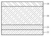
도 2는 본 발명의 일 구현예에 따른 비휘발성 메모리 소자의 스토리지 노드의 구조를 나타내는 단면도이다.2 is a cross-sectional view illustrating a structure of a storage node of a nonvolatile memory device according to an embodiment of the present invention.
도 3a 내지 도 3d는 본 발명의 일 구현예에 따른 스토리지 노드의 제조방법을 나타내는 공정 단면도 이다.3A to 3D are cross-sectional views illustrating a method of manufacturing a storage node according to an embodiment of the present invention.
도 4는 본 발명의 일 구현예에 따른 비휘발성 메모리 소자의 스위칭 특성을 나타내는 I-V 커브의 그래프이다.4 is a graph of an I-V curve showing switching characteristics of a nonvolatile memory device according to an embodiment of the present invention.
도 5는 종래 기술에 따른 비휘발성 메모리 소자의 메모리 스위칭 특성을 나타내는 I-V 커브의 그래프이다.5 is a graph of an I-V curve showing memory switching characteristics of a nonvolatile memory device according to the prior art.
도 6는 본 발명의 일 구현예에 따른 비휘발성 메모리 소자에 인가되는 셋/리셋 전압값 분포를 보여주는 그래프이다.6 is a graph illustrating a distribution of set / reset voltage values applied to a nonvolatile memory device according to an exemplary embodiment of the present invention.
도 7은 종래 기술에 따른 비휘발성 메모리 소자에 인가되는 셋/리셋 전압값 분포를 보여주는 그래프이다.7 is a graph illustrating a distribution of set / reset voltage values applied to a nonvolatile memory device according to the related art.
도 8은 본 발명의 일 구현예에 따른 비휘발성 메모리 소자의 스위칭시 온/오프 상태에 따른 스토리지 노드의 저항값 분포를 보여주는 그래프이다.FIG. 8 is a graph illustrating a distribution of resistance values of a storage node according to an on / off state when switching a nonvolatile memory device according to an exemplary embodiment of the present invention.
도 9는 종래 기술에 따른 비휘발성 메모리 소자의 스위칭시 온/오프 상태에 따른 스토리지 노드의 저항값 분포를 보여주는 그래프이다.9 is a graph illustrating a resistance distribution of a storage node according to an on / off state when switching a nonvolatile memory device according to the related art.
< 도면의 주요부분에 대한 부호의 설명 >Description of the Related Art
12,22,32... 하부전극 14,24,34... 산소 결핍 금속산화물층12,22,32 ...
16,26,36... 데이터 저장층 18,28,38... 상부전극16,26,36 ...
19... 스토리지 노드 30,100... 기판19 ... Storage Node 30,100 ... Board
103... 게이트절연막 105... 게이트전극103 ... gate
107C... 채널 107S... 소오스107C ... Channel 107S ... Source
107D... 드레인 109... 절연층107 D ... Drain 109 ... Insulation Layer
111... 플레이트전극 113... 콘택트플러그(contact plug)111
115... 트랜지스터115 ... transistor
본 발명은 산소결핍 금속산화물을 이용한 비휘발성 메모리 소자 및 그 제조방법에 관한 것으로, 보다 상세하게는 하부전극과 데이터 저장층 사이에 산소결핍 금속산화물층을 형성한 스토리지 노드를 구비하는 비휘발성 메모리 소자 및 그 제조방법에 관한 것이다.The present invention relates to a nonvolatile memory device using an oxygen deficient metal oxide and a method of manufacturing the same, and more particularly, to a nonvolatile memory device including a storage node having an oxygen depleted metal oxide layer formed between a lower electrode and a data storage layer. And to a method for producing the same.
기존의 DRAM 공정은 1T(transistor)/1 C(capacitor)구조의 단위셀을 이루고 있는데, 소자의 크기가 작아짐에 따라, 캐패시터 공정의 난이도가 증가하여, 높은 수율을 가지는 DRAM 셀의 제작이 어렵게 된다. 그래서 기존 DRAM을 대체할 수 있고, 비휘발성을 가지는 메모리의 필요성이 크게 요구되고 있다. 현재 개발되고 있는 차세대 메모리는 DRAM의 고집적성과 낮은 소비전력, 플래쉬 메모리의 비휘발성, SRAM의 고속 동작을 모두 구현하기 위한 시도가 이루어지고 있다. 차세대 메모리로 유력하게 대두되고 있는 소자는 PRAM(phase change RAM), NFGM(nano floating gate memory), ReRAM(resistance RAM), PoRAM(polymer RAM), MRAM (magnetic RAM), 분자전자 소자 등이 있다.Conventional DRAM processes form unit cells of 1T (transistor) / 1 C (capacitor) structure. As the size of devices decreases, the difficulty of the capacitor process increases, making it difficult to manufacture DRAM cells having high yields. . Therefore, there is a great demand for a memory that can replace existing DRAM and has a nonvolatile memory. The next generation of memory currently being developed is attempting to realize both high integration and low power consumption of DRAM, nonvolatile flash memory, and high speed operation of SRAM. Devices that are emerging as next-generation memories include phase change RAM (PRAM), nano floating gate memory (NFGM), resistance RAM (ReRAM), polymer RAM (PoRAM), magnetic RAM (MRAM), and molecular electronic devices.
이중에서 ReRAM 소자는 금속산화물을 이용한 MIM구조로서 적당한 전기적 신호를 가하면 저항이 큰 전도가 되지 않는 상태(off state)에서 저항이 작은 전도가 가능한 상태(on state)로 바뀌는 메모리 특성이 나타난다. 여기에서 M은 금속재질의 상부 및 하부전극을 지칭하며, I는 저항체 물질로 구성된 데이터 저장층을 지칭한다.Among them, the ReRAM device is a MIM structure using a metal oxide. When a proper electrical signal is applied, the ReRAM device exhibits a memory characteristic of changing from an off state in which the resistance does not become large to an on state. Here, M refers to the upper and lower electrodes of the metal material, and I refers to the data storage layer made of a resistive material.
종래의 MIM 메모리 셀 구조의 스토리지 노드에서는 반복적인 스위칭시에 스토리지 노드에 인가되는 셋(set)/리셋(reset) 전압값 (Vset,Vreset)의 분포편차가 크고, 온(on)/오프(off) 상태에 따른 스토리지 노드의 저항값(Ron,Roff) 분포가 균일하지 못하다는 문제점이 있다.In the storage node of the conventional MIM memory cell structure, the distribution deviation of theset / reset voltage values (Vset and Vreset ) applied to the storage node during repetitive switching is large, and is turned on / off. There is a problem that the distribution of the resistance values (Ron , Roff ) of the storage node according to the (off) state is not uniform.
본 발명의 목적은 스토리지 노드에서 안정적인 메모리 스위칭 특성을 갖도록 그 구조가 개선된 비휘발성 메모리 소자를 제공하는 것이다.An object of the present invention is to provide a nonvolatile memory device whose structure is improved to have stable memory switching characteristics in a storage node.
본 발명의 다른 목적은 상기 스토리지 노드를 구비하는 비휘발성 메모리 소자의 제조방법을 제공하는 것이다.Another object of the present invention is to provide a method of manufacturing a nonvolatile memory device having the storage node.
상기의 목적을 달성하기 위하여 본 발명은 스위칭 소자와 상기 스위칭 소자에 연결된 스토리지 노드를 구비하는 비휘발성 메모리 소자에 있어서 상기 스토리지 노드는, 하부전극; 상기 하부전극 상에 형성된 산소 결핍 금속산화물층; 상기 산소 결핍 금속산화물층 상에 형성된 데이터 저장층; 및 상기 데이터 저장층 상에 형성된 상부전극을 포함하는 것을 특징으로 하는 비휘발성 메모리 소자를 제공한다. 여기에서, 상기 스위칭 소자는 트랜지스터 또는 다이오드를 포함한다.In order to achieve the above object, the present invention provides a nonvolatile memory device including a switching device and a storage node connected to the switching device, wherein the storage node comprises: a lower electrode; An oxygen depleted metal oxide layer formed on the lower electrode; A data storage layer formed on the oxygen depleted metal oxide layer; And an upper electrode formed on the data storage layer. Here, the switching element includes a transistor or a diode.
본 발명에 있어서, 상기 산소 결핍 금속산화물층은 산소 베이컨시(vacancy)가 포함된 금속산화물층이며, 전도성 금속산화물 보다 비저항이 크고, 데이터 저장층 보다 비저항이 작은 것을 특징으로 한다.In the present invention, the oxygen depletion metal oxide layer is a metal oxide layer containing oxygen vacancies (vacancy), characterized in that the specific resistance is larger than the conductive metal oxide, and the specific resistance is smaller than the data storage layer.
본 발명에 있어서, 상기 산소 결핍 금속산화물층은 ZnO, ITO, IZO, ZrO 및 RuO2으로 이루어진 군에서 선택된 어느 하나 인 것을 특징으로 한다.In the present invention, the oxygen deficient metal oxide layer is characterized in that any one selected from the group consisting of ZnO, ITO, IZO, ZrO and RuO2.
본 발명에 있어서, 상기 산소 결핍 금속산화물층은 ZnO, ITO, IZO, ZrO 및 RuO2으로 이루어진 군에서 선택된 어느 하나 인 것을 특징으로 한다.In the present invention, the oxygen deficient metal oxide layer is characterized in that any one selected from the group consisting of ZnO, ITO, IZO, ZrO and RuO2.
본 발명에 있어서, 상기 산소 결핍 금속산화물층은 ZnO층인 것을 특징으로 한다.In the present invention, the oxygen depleted metal oxide layer is characterized in that the ZnO layer.
본 발명에 있어서. 상기 ZnO층의 두께는 1내지 50nm인 것을 특징으로 한다.In the present invention. The thickness of the ZnO layer is characterized in that 1 to 50nm.
본 발명에 있어서, 상기 상부 및 하부전극은 Pt,Ru,Ir,Pd,Au,Cr,Ni,Cu 및 TiN으로 이루어진 군에서 선택된 어느 하나 인 것을 특징으로 한다.In the present invention, the upper and lower electrodes are any one selected from the group consisting of Pt, Ru, Ir, Pd, Au, Cr, Ni, Cu and TiN.
본 발명에 있어서, 상기 하부전극은 Ru인 것을 특징으로 한다.In the present invention, the lower electrode is characterized in that Ru.
본 발명에 있어서, 상기 데이터 저장층은 NiO, Nb2O5, TiO2, Al2O3, V2O5, WO3, ZnO 및 CoO로 이루어진 군에서 선택된 어느 하나인 것을 특징으로 한다.In the present invention, the data storage layer is characterized in that any one selected from the group consisting of NiO, Nb2 O5 , TiO2 , Al2 O3 , V2 O5 ,
본 발명의 일 구현예에 따르면 상기 산소 결핍 금속산화물층은 바람직하게는 ZnO층이다.According to one embodiment of the invention the oxygen depleted metal oxide layer is preferably a ZnO layer.
상기 다른 목적을 달성하기 위하여 본 발명은 스위칭 소자를 준비하는 단계; 상기 스위칭 소자에 연결되는 스토리지 노드의 하부 전극을 형성하는 단계; 상기 하부전극 상에 산소 결핍 금속산화물층을 형성하는 단계; 상기 산소 결핍 금속산화물층 상에 데이터 저장층을 형성하는 단계; 및 상기 데이터 저장층 상에 상부전극을 형성하는 단계를 포함하는 비휘발성 메모리 소자의 제조방법을 제공한다. 여기에서, 상기 스위칭 소자는 트랜지스터 또는 다이오드를 포함한다.In order to achieve the above another object, the present invention comprises the steps of preparing a switching device; Forming a bottom electrode of a storage node connected to the switching element; Forming an oxygen depleted metal oxide layer on the lower electrode; Forming a data storage layer on the oxygen depleted metal oxide layer; And forming an upper electrode on the data storage layer. Here, the switching element includes a transistor or a diode.
이하, 첨부된 도면을 참조하여 본 발명에 대하여 보다 상세히 설명한다.Hereinafter, with reference to the accompanying drawings will be described in more detail with respect to the present invention.
도 1은 본 발명의 일 구현예에 따른 비휘발성 메모리 소자의 개략적 단면도이다.1 is a schematic cross-sectional view of a nonvolatile memory device according to an embodiment of the present invention.
도 1을 참조하면, 비휘발성 메모리 소자는 트랜지스터(115)와 이에 연결된 스토리지 노드(19)를 구비한다. 상기 트랜지스터(115)는 소오스(107S), 드레 인(107D), 채널(107C) 및 게이트전극(105)을 포함한다. 상기 스토리지 노드(19)는 상부전극(18), 하부전극(12) 및 이들 사이에 개재된 데이터 저장층(16)을 포함하며, 상기 스토리지 노드(19)와 트랜지스터(115) 사이에 절연층(109)이 개재된다. 그리고 상기 스토리지 노드(19)는 도전성의 콘택트 플러그(113)에 의해 상기 트랜지스터(115)와 연결되며 상기 상부전극(18)위에 플레이트전극(111)이 배치된다.Referring to FIG. 1, a nonvolatile memory device includes a
도 2는 본 발명의 일 구현예에 따른 스토리지 노드의 구조를 나타내는 단면도이다.2 is a cross-sectional view illustrating a structure of a storage node according to an embodiment of the present invention.
도 2를 참조하면, 본 발명의 일 구현예에 따른 비휘발성 메모리 소자에 포함되는 스토리지 노드는 하부전극(22), 상기 하부전극 상에 형성된 산소 결핍 금속산화물층(24), 상기 산소 결핍 금속산화물층(24) 상에 형성된 데이터 저장층(26); 및 상기 데이터 저장층(26) 상에 형성된 상부전극(28)을 포함하여 이루어진다.2, a storage node included in a nonvolatile memory device according to an embodiment of the present invention may include a
상기 상부(28) 및 하부전극(22)은 Pt, Ru, Ir, Pd, Au, Cr, Ni, Cu 및 TiN으로 이루어진 군에서 선택된 일종 이상의 물질로 형성될 수 있으며, 바람직하게는 상부 전극으로는 Pt, 하부 전극으로는 Ru를 사용한다. 상기 상부 및 하부전극은 스퍼터링법, 전자빔증착법 및 화학기상증착법의 방법으로 형성할 수 있다. 이때 전극의 두께는 10내지 200nm의 범위가 되는 것이 바람직하다.The upper 28 and the
상기 하부 전극(22) 상에 형성되는 산소 결핍 금속산화물층(24)은 산소 베이컨시를 포함하고 있는 금속산화물층을 지칭하는 것으로, 금속 산화물내에 포함된 산소 베이컨시는 전압 인가시 산소를 흡수하는 역할을 하며, 데이터 저장층(26)과 금속 산화물층(24) 계면에 집합된 산소는 금속필라멘트의 단락에 영향을 주어 메모 리의 스위칭 특성을 향상시키는 것으로 예측된다.The oxygen depleted
상기 산소 결핍 금속산화물층(24)은 구체적으로는 ZnO, ITO, IZO, ZrO, RuO2 등의 금속 산화물로 이루어질 수 있으며, 그 두께는 약 1 내지 50nm의 범위이다. 산소결핍 금속산화물층의 두께가 50nm를 초과하는 경우 메모리 스위칭 특성의 향상을 기대하기 어렵다.Specifically, the oxygen depleted
상기 산소 결핍 금속산화물층(24)은 스퍼터링법, 펄스레이저증착법, 화학기상증착법, 유기금속기상증착법, 졸겔법 및 스프레이 열분해법으로 형성할 수 있다.The oxygen depleted
상기 산소 결핍 금속산화물층(24)은 바람직하게는 ZnO로 이루어진다.The oxygen depleted
ZnO는 공정조건 및 형성방법에 따라 절연체, 반도체 또는 전도체를 형성할 수 있는데, ZnO 박막 형성 시 산소분압에 따라 그 전도도 및 산소 베이컨시 형성 정도가 변화한다. 구체적으로는 낮은 산소분압 조건하에서 형성한 ZnO층 내에는 산소 베이컨시가 다량 형성되는 것으로 알려져 있다. 상기와 같이 ZnO는 산소 베이컨시 형성과 함께 전도도 특성을 조절 할 수 있어 바람직하다.ZnO can form an insulator, semiconductor, or conductor according to process conditions and formation methods. The conductivity and the degree of oxygen vacancy formation change according to the partial pressure of oxygen when forming a ZnO thin film. Specifically, it is known that a large amount of oxygen vacancy is formed in the ZnO layer formed under low oxygen partial pressure conditions. As described above, ZnO is preferable because it can control the conductivity characteristics along with oxygen vacancy formation.
ZnO를 사용하여 산소결핍 금속 산화물층을 형성하고자 하는 경우 ZnO 타겟을 원료로 산소가스를 추가로 투입하여 산소 분압 50%이하, 온도 50℃이하에서 반응성 스퍼터링법으로 형성하는 것이 바람직하다.In order to form an oxygen depleted metal oxide layer using ZnO, it is preferable to form an ZnO target by additionally adding oxygen gas as a raw material to form a reactive sputtering method at an oxygen partial pressure of 50% or less and a temperature of 50 ° C or less.
상기 데이터 저장층(26)은 가변 저항 특성을 지닌 전이 금속 산화물을 사용하는 것이 바람직하다. 구체적으로 예를 들면, NiO, Nb2O5, TiO2, Al2O3, V2O5, WO3, ZnO 및 CoO로 이루어진 군에서 선택된 어느 하나의 물질로 이루어질 수 있다.The
도 3a 내지 도 3d는 본 발명의 일 구현예에 따른 비휘발성 메모리에포함된 스토리지 노드 제조방법을 나타내는 공정 단면도이다. 비휘발성 메모리에 있어서 소스, 드레인, 채널 및 게이트 전극을 포함하는 반도체 스위칭 소자의 형성 방법은 널리 알려져 있으므로 이에 대한 상세한 설명은 생략하기로 한다.3A to 3D are cross-sectional views illustrating a method of manufacturing a storage node included in a nonvolatile memory according to an embodiment of the present invention. Since a method of forming a semiconductor switching device including a source, a drain, a channel, and a gate electrode in a nonvolatile memory is widely known, a detailed description thereof will be omitted.
도 3a를 참조하면, 먼저, 실리콘 기판(30) 상에 하부전극(32)을 형성한다. 상기 하부전극(32)은 Pt, Ru, Ir, Pd, Au, Cr, Ni, Cu 및 TiN으로 이루어진 군에서 선택된 일종 이상의 물질로 형성될 수 있으며, 바람직하게는 Ru를 사용한다. 상기 하부전극(32)은 스퍼터링법, 전자빔증착법 및 화학기상증착법의 방법으로 형성할 수 있으며, 전극의 두께는 10내지 200nm의 범위가 되는 것이 바람직하다.Referring to FIG. 3A, first, a
다음으로, 도 3b를 참조하면 상기의 하부전극(32) 상에 산소 결핍 금속산화물층(34)을 형성한다. 산소 결핍 금속 산화물층은 ZnO, ITO, IZO, ZrO, RuO2등의 금속 산화물로 이루어질 수 있으며, 그 두께는 약 1 내지 50nm의 범위로 형성한다.Next, referring to FIG. 3B, an oxygen depletion
상기 산소 결핍 금속산화물층(24)은 스퍼터링법, 펄스레이저증착법, 화학기상증착법, 유기금속기상증착법, 졸겔법 또는 스프레이 열분해법으로 형성할 수 있다.The oxygen depleted
다음으로 도 3c 및 3d를 참조하면, 상기 산소 결핍 금속산화물층(34) 위에 데이터 저장층(36)을 형성하고 그 위에 상부전극(38)을 형성한다.3C and 3D, a
상기 데이터 저장층(36)은 NiO, Nb2O5, TiO2, Al2O3, V2O5, WO3, ZnO 및 CoO로 이루어진 군에서 선택된 어느 하나의 물질로 이루어질 수 있다.The
상기 상부전극(38) 상기 하부전극(32)과 동일한 재질로 형성될 수 있으며, 바람직하게는 Pt를 사용한다.The upper electrode 38 may be formed of the same material as the
도 4는 본 발명의 일 구현예에 따른 Pt/NiO/ZnO/Ru 구조의 스토리지 노드를 포함하는 메모리의 스위칭 특성을 나타내는 I-V 커브의 그래프이고, 도 5는 종래 기술에 따른 산소 결핍 금속산화물층이 생략된 Pt/NiO/Pt 구조의 스토리지 노드를 포함하는 메모리의 스위칭 특성을 나타내는 I-V 커브의 그래프이다.4 is a graph of an IV curve showing switching characteristics of a memory including a storage node having a Pt / NiO / ZnO / Ru structure according to an embodiment of the present invention, and FIG. 5 is an oxygen depleted metal oxide layer according to the prior art. A graph of an IV curve showing switching characteristics of a memory including a storage node of a Pt / NiO / Pt structure, which is omitted.
도 4와 도 5를 참조하면, 도 4의 Pt/NiO/ZnO/Ru 구조의 스토리지 노드는 인가되는 셋/리셋 전압값(Vset,Vreset)의 분포편차가 도 5의 종래의 Pt/NiO/Pt 구조의 경우와 비교하여 균일하고 안정적으로 구현된다. 여기에서 Vset은 셋 전이(set transition) 하는 전압이고, Vreset은 리셋 전이(reset transition) 할 때 보이는 최고전류 피크에서의 전압이다.4 and 5, in the storage node of the Pt / NiO / ZnO / Ru structure of FIG. 4, the distribution deviation of the set / reset voltage values (Vset, Vreset) applied to the Pt / NiO / Pt structure of FIG. Compared to the case of the structure is implemented uniformly and stably. Where Vset is the voltage at which the set transition occurs, and Vreset is the voltage at the highest current peak seen at the reset transition.
도 6은 본 발명의 일 구현예에 따른 Pt/NiO/ZnO/Ru 구조의 스토리지 노드에 인가되는 셋/리셋 전압값 분포를 보여주는 그래프이고, 도 7은 종래 기술에 따른 Pt/NiO/Pt 구조의 스토리지 노드에 인가되는 셋/리셋 전압값 분포를 보여주는 그래프이다.FIG. 6 is a graph illustrating a distribution of set / reset voltage values applied to a storage node having a Pt / NiO / ZnO / Ru structure according to an embodiment of the present invention, and FIG. 7 is a view illustrating a Pt / NiO / Pt structure according to the related art. This graph shows the distribution of set / reset voltage values applied to the storage node.
도 6 내지 도 7을 참조하면, 본 발명에 따른 Pt/NiO/ZnO/Ru 구조의 스토리지 노드에서 스위칭 사이클에 대한 Vset 및 Vreset의 표준편차가 종래의 Pt/NiO/Pt 구조에서의 표준편차보다 감소한 것을 확인할 수 있다.6 to 7, the standard deviation of Vset and Vreset with respect to the switching cycle in the storage node of the Pt / NiO / ZnO / Ru structure according to the present invention is reduced than the standard deviation in the conventional Pt / NiO / Pt structure You can see that.
도 8은 본 발명의 일 구현예에 따른 Pt/NiO/ZnO/Ru 구조의 스토리지 노드 스위칭 시 온/오프 상태에 따른 스토리지 노드의 저항값 분포를 보여주는 그래프이 고, 도 9는 종래 기술에 따른 Pt/NiO/Pt 구조의 스토리지 노드 스위칭시 온/오프 상태에 따른 스토리지 노드의 저항값 분포를 보여주는 그래프이다.FIG. 8 is a graph showing a distribution of resistance values of storage nodes according to on / off states when switching storage nodes having a Pt / NiO / ZnO / Ru structure according to an embodiment of the present invention, and FIG. 9 is a Pt / This graph shows the distribution of resistance values of storage nodes according to on / off states when switching storage nodes of NiO / Pt structure.
도 8 내지 도 9를 참조하면, 본 발명에 따른 Pt/NiO/ZnO/Ru 구조의 스토리지 노드에서 스위칭 사이클에 대한 Ron 및 Roff의 표준편차가 Pt/NiO/Pt 구조에서의 표준편차보다 감소한 것을 확인할 수 있다. 이로써, 본 발명에 따른 스토리지 노드 구조에서 Ron 및 Roff의 표준편차가 감소하여 메모리 특성이 향상된 것을 알 수 있다.8 to 9, it is confirmed that the standard deviation of Ron and Roff with respect to the switching cycle in the storage node of the Pt / NiO / ZnO / Ru structure according to the present invention is reduced from the standard deviation in the Pt / NiO / Pt structure. Can be. As a result, it can be seen that the memory characteristics are improved by reducing the standard deviation of Ron and Roff in the storage node structure according to the present invention.
이상에서 설명한 바와 같이, 본 발명은 산소 결핍 금속산화물을As described above, the present invention provides an oxygen depleted metal oxide.
스토리지 노드에 도입하여 안정적인 메모리 스위칭 특성을 가질 수 있다.Introduced in the storage node can have a stable memory switching characteristics.
상세하게는 반복 스위칭시, 스토리지 노드에 인가되는 셋/리셋 전압Specifically, the set / reset voltage applied to the storage node during repetitive switching
표준편차 및 온/오프 상태에 따른 저항 표준편차를 감소시킬 수 있는 효과가It is effective to reduce the standard deviation and standard deviation of resistance due to on / off state.
있다.have.
이상에서 본 발명은 기재된 구체 예에 대해서만 상세히 설명되었지만 본 발명의 기술적 사상 범위 내에서 다양한 변형 및 수정이 가능함은 당업자에게 있어서 명백한 것이며, 이러한 변형 및 수정이 첨부된 특허청구범위에 속함은 당연한 것이다.Although the present invention has been described in detail only with respect to the described embodiments, it will be apparent to those skilled in the art that various changes and modifications can be made within the spirit of the present invention, and such modifications and modifications belong to the appended claims.
Claims (19)
Translated fromKoreanPriority Applications (6)
| Application Number | Priority Date | Filing Date | Title |
|---|---|---|---|
| KR1020060045154AKR101206034B1 (en) | 2006-05-19 | 2006-05-19 | Nonvolatile memory device using oxygen-deficient metal oxide layer and the fabrication method |
| CN200610165950.5ACN101075629B (en) | 2006-05-19 | 2006-12-11 | Nonvolatile memory device using oxygen-deficient metal oxide layer and method of manufacturing the same |
| EP07102983.9AEP1858074B1 (en) | 2006-05-19 | 2007-02-23 | Nonvolatile memory device using oxygen-deficient metal oxide layer and method of manufacturing the same |
| JP2007130912AJP2007311798A (en) | 2006-05-19 | 2007-05-16 | Nonvolatile memory device using oxygen-deficient metal oxide and manufacturing method thereof |
| US11/798,703US7842991B2 (en) | 2006-05-19 | 2007-05-16 | Nonvolatile memory devices including oxygen-deficient metal oxide layers and methods of manufacturing the same |
| US12/926,042US8043926B2 (en) | 2006-05-19 | 2010-10-22 | Nonvolatile memory devices including oxygen-deficient metal oxide layers and methods of manufacturing the same |
Applications Claiming Priority (1)
| Application Number | Priority Date | Filing Date | Title |
|---|---|---|---|
| KR1020060045154AKR101206034B1 (en) | 2006-05-19 | 2006-05-19 | Nonvolatile memory device using oxygen-deficient metal oxide layer and the fabrication method |
Publications (2)
| Publication Number | Publication Date |
|---|---|
| KR20070111840A KR20070111840A (en) | 2007-11-22 |
| KR101206034B1true KR101206034B1 (en) | 2012-11-28 |
Family
ID=38515433
Family Applications (1)
| Application Number | Title | Priority Date | Filing Date |
|---|---|---|---|
| KR1020060045154AExpired - Fee RelatedKR101206034B1 (en) | 2006-05-19 | 2006-05-19 | Nonvolatile memory device using oxygen-deficient metal oxide layer and the fabrication method |
Country Status (5)
| Country | Link |
|---|---|
| US (2) | US7842991B2 (en) |
| EP (1) | EP1858074B1 (en) |
| JP (1) | JP2007311798A (en) |
| KR (1) | KR101206034B1 (en) |
| CN (1) | CN101075629B (en) |
Families Citing this family (83)
| Publication number | Priority date | Publication date | Assignee | Title |
|---|---|---|---|---|
| US7082052B2 (en) | 2004-02-06 | 2006-07-25 | Unity Semiconductor Corporation | Multi-resistive state element with reactive metal |
| US20060171200A1 (en) | 2004-02-06 | 2006-08-03 | Unity Semiconductor Corporation | Memory using mixed valence conductive oxides |
| US8559209B2 (en) | 2011-06-10 | 2013-10-15 | Unity Semiconductor Corporation | Array voltage regulating technique to enable data operations on large cross-point memory arrays with resistive memory elements |
| US8565003B2 (en) | 2011-06-28 | 2013-10-22 | Unity Semiconductor Corporation | Multilayer cross-point memory array having reduced disturb susceptibility |
| US8937292B2 (en) | 2011-08-15 | 2015-01-20 | Unity Semiconductor Corporation | Vertical cross point arrays for ultra high density memory applications |
| US20130082232A1 (en) | 2011-09-30 | 2013-04-04 | Unity Semiconductor Corporation | Multi Layered Conductive Metal Oxide Structures And Methods For Facilitating Enhanced Performance Characteristics Of Two Terminal Memory Cells |
| US8270193B2 (en) | 2010-01-29 | 2012-09-18 | Unity Semiconductor Corporation | Local bit lines and methods of selecting the same to access memory elements in cross-point arrays |
| KR100982424B1 (en)* | 2006-11-28 | 2010-09-15 | 삼성전자주식회사 | Method of manufacturing resistive memory device |
| CN101711431B (en)* | 2007-05-09 | 2015-11-25 | 分子间公司 | Resistive non-volatile memory element |
| JP5263160B2 (en)* | 2007-08-22 | 2013-08-14 | 富士通株式会社 | Variable resistance element |
| US8946020B2 (en) | 2007-09-06 | 2015-02-03 | Spansion, Llc | Method of forming controllably conductive oxide |
| KR100929730B1 (en)* | 2007-12-27 | 2009-12-03 | 주식회사 동부하이텍 | Nonvolatile Memory Cell Manufacturing Method |
| US7768812B2 (en) | 2008-01-15 | 2010-08-03 | Micron Technology, Inc. | Memory cells, memory cell programming methods, memory cell reading methods, memory cell operating methods, and memory devices |
| US8373149B2 (en)* | 2008-04-07 | 2013-02-12 | Nec Corporation | Resistance change element and manufacturing method thereof |
| US8034655B2 (en) | 2008-04-08 | 2011-10-11 | Micron Technology, Inc. | Non-volatile resistive oxide memory cells, non-volatile resistive oxide memory arrays, and methods of forming non-volatile resistive oxide memory cells and memory arrays |
| US8551809B2 (en)* | 2008-05-01 | 2013-10-08 | Intermolecular, Inc. | Reduction of forming voltage in semiconductor devices |
| US8211743B2 (en) | 2008-05-02 | 2012-07-03 | Micron Technology, Inc. | Methods of forming non-volatile memory cells having multi-resistive state material between conductive electrodes |
| US8134865B2 (en)* | 2008-05-06 | 2012-03-13 | Macronix International Co., Ltd. | Operating method of electrical pulse voltage for RRAM application |
| CN101689548B (en)* | 2008-05-08 | 2012-06-13 | 松下电器产业株式会社 | Nonvolatile storage element, nonvolatile storage device, and data writing method to nonvolatile storage element |
| US8134137B2 (en) | 2008-06-18 | 2012-03-13 | Micron Technology, Inc. | Memory device constructions, memory cell forming methods, and semiconductor construction forming methods |
| US9343665B2 (en) | 2008-07-02 | 2016-05-17 | Micron Technology, Inc. | Methods of forming a non-volatile resistive oxide memory cell and methods of forming a non-volatile resistive oxide memory array |
| CN101836296B (en)* | 2008-08-20 | 2012-09-19 | 松下电器产业株式会社 | Resistance variable nonvolatile memory device and method for forming memory cell |
| JP5338236B2 (en)* | 2008-10-01 | 2013-11-13 | パナソニック株式会社 | NONVOLATILE MEMORY ELEMENT AND METHOD FOR MANUFACTURING SAME, NONVOLATILE MEMORY DEVICE USING THE NONVOLATILE MEMORY ELEMENT AND METHOD FOR MANUFACTURING SAME |
| JP4607257B2 (en) | 2008-12-04 | 2011-01-05 | パナソニック株式会社 | Nonvolatile memory element and nonvolatile memory device |
| CN102227809A (en)* | 2008-12-04 | 2011-10-26 | 松下电器产业株式会社 | non-volatile storage element |
| WO2010064444A1 (en)* | 2008-12-05 | 2010-06-10 | パナソニック株式会社 | Nonvolatile memory element and manufacturing method therefor |
| KR101526926B1 (en)* | 2008-12-30 | 2015-06-10 | 삼성전자주식회사 | Resist RAM and method of manufacturing the same |
| CN101960595B (en)* | 2009-02-04 | 2012-11-14 | 松下电器产业株式会社 | Non-volatile memory element |
| WO2010118380A2 (en)* | 2009-04-10 | 2010-10-14 | Intermolecular, Inc. | Resistive-switching memory elements having improved switching characteristics |
| KR101133707B1 (en)* | 2009-09-02 | 2012-04-13 | 에스케이하이닉스 주식회사 | Resistive memory device and method for manufacturing the same |
| KR101055748B1 (en) | 2009-10-23 | 2011-08-11 | 주식회사 하이닉스반도체 | Resistance change device and manufacturing method thereof |
| CN102414819A (en)* | 2009-11-02 | 2012-04-11 | 松下电器产业株式会社 | Variable resistance non-volatile memory device, and method of forming memory cell |
| KR20110072920A (en) | 2009-12-23 | 2011-06-29 | 삼성전자주식회사 | Resistive memory devices |
| US8563962B2 (en)* | 2009-12-28 | 2013-10-22 | Panasonic Corporation | Memory device and method of manufacturing the same |
| US8638584B2 (en) | 2010-02-02 | 2014-01-28 | Unity Semiconductor Corporation | Memory architectures and techniques to enhance throughput for cross-point arrays |
| US8437174B2 (en)* | 2010-02-15 | 2013-05-07 | Micron Technology, Inc. | Memcapacitor devices, field effect transistor devices, non-volatile memory arrays, and methods of programming |
| US8416609B2 (en) | 2010-02-15 | 2013-04-09 | Micron Technology, Inc. | Cross-point memory cells, non-volatile memory arrays, methods of reading a memory cell, methods of programming a memory cell, methods of writing to and reading from a memory cell, and computer systems |
| WO2011109019A1 (en)* | 2010-03-03 | 2011-09-09 | Hewlett-Packard Development Company, L.P. | Resistive switches |
| WO2011114725A1 (en)* | 2010-03-19 | 2011-09-22 | パナソニック株式会社 | Nonvolatile memory element, production method therefor, design support method therefor, and nonvolatile memory device |
| US8362477B2 (en)* | 2010-03-23 | 2013-01-29 | International Business Machines Corporation | High density memory device |
| US8411477B2 (en) | 2010-04-22 | 2013-04-02 | Micron Technology, Inc. | Arrays of vertically stacked tiers of non-volatile cross point memory cells, methods of forming arrays of vertically stacked tiers of non-volatile cross point memory cells, and methods of reading a data value stored by an array of vertically stacked tiers of non-volatile cross point memory cells |
| US8427859B2 (en) | 2010-04-22 | 2013-04-23 | Micron Technology, Inc. | Arrays of vertically stacked tiers of non-volatile cross point memory cells, methods of forming arrays of vertically stacked tiers of non-volatile cross point memory cells, and methods of reading a data value stored by an array of vertically stacked tiers of non-volatile cross point memory cells |
| KR20110132125A (en) | 2010-06-01 | 2011-12-07 | 삼성전자주식회사 | Nonvolatile Memory Device and Formation Method of Nonvolatile Memory Device |
| US8289763B2 (en) | 2010-06-07 | 2012-10-16 | Micron Technology, Inc. | Memory arrays |
| US8634224B2 (en) | 2010-08-12 | 2014-01-21 | Micron Technology, Inc. | Memory cells, non-volatile memory arrays, methods of operating memory cells, methods of writing to and reading from a memory cell, and methods of programming a memory cell |
| US8804398B2 (en)* | 2010-08-20 | 2014-08-12 | Shine C. Chung | Reversible resistive memory using diodes formed in CMOS processes as program selectors |
| US8351242B2 (en) | 2010-09-29 | 2013-01-08 | Micron Technology, Inc. | Electronic devices, memory devices and memory arrays |
| US8759809B2 (en) | 2010-10-21 | 2014-06-24 | Micron Technology, Inc. | Integrated circuitry comprising nonvolatile memory cells having platelike electrode and ion conductive material layer |
| US8526213B2 (en) | 2010-11-01 | 2013-09-03 | Micron Technology, Inc. | Memory cells, methods of programming memory cells, and methods of forming memory cells |
| US8796661B2 (en) | 2010-11-01 | 2014-08-05 | Micron Technology, Inc. | Nonvolatile memory cells and methods of forming nonvolatile memory cell |
| US9454997B2 (en) | 2010-12-02 | 2016-09-27 | Micron Technology, Inc. | Array of nonvolatile memory cells having at least five memory cells per unit cell, having a plurality of the unit cells which individually comprise three elevational regions of programmable material, and/or having a continuous volume having a combination of a plurality of vertically oriented memory cells and a plurality of horizontally oriented memory cells; array of vertically stacked tiers of nonvolatile memory cells |
| US8431458B2 (en) | 2010-12-27 | 2013-04-30 | Micron Technology, Inc. | Methods of forming a nonvolatile memory cell and methods of forming an array of nonvolatile memory cells |
| US8791447B2 (en) | 2011-01-20 | 2014-07-29 | Micron Technology, Inc. | Arrays of nonvolatile memory cells and methods of forming arrays of nonvolatile memory cells |
| CN102646790B (en)* | 2011-02-18 | 2014-06-04 | 华邦电子股份有限公司 | Non-volatile memory |
| US8488365B2 (en) | 2011-02-24 | 2013-07-16 | Micron Technology, Inc. | Memory cells |
| CN102683583B (en)* | 2011-03-15 | 2014-04-09 | 北京大学 | Unipolar resistive random access memory and manufacturing method thereof |
| US8537592B2 (en) | 2011-04-15 | 2013-09-17 | Micron Technology, Inc. | Arrays of nonvolatile memory cells and methods of forming arrays of nonvolatile memory cells |
| US9117495B2 (en) | 2011-06-10 | 2015-08-25 | Unity Semiconductor Corporation | Global bit line pre-charge circuit that compensates for process, operating voltage, and temperature variations |
| US10566056B2 (en) | 2011-06-10 | 2020-02-18 | Unity Semiconductor Corporation | Global bit line pre-charge circuit that compensates for process, operating voltage, and temperature variations |
| US8891276B2 (en) | 2011-06-10 | 2014-11-18 | Unity Semiconductor Corporation | Memory array with local bitlines and local-to-global bitline pass gates and gain stages |
| US8288297B1 (en)* | 2011-09-01 | 2012-10-16 | Intermolecular, Inc. | Atomic layer deposition of metal oxide materials for memory applications |
| WO2013061559A1 (en) | 2011-10-24 | 2013-05-02 | パナソニック株式会社 | Nonvolatile storage cell and nonvolatile storage device |
| CN102543886B (en)* | 2012-01-05 | 2014-09-03 | 复旦大学 | Manufacturing method of gated diode semiconductor memory device |
| US8581224B2 (en) | 2012-01-20 | 2013-11-12 | Micron Technology, Inc. | Memory cells |
| US8878152B2 (en)* | 2012-02-29 | 2014-11-04 | Intermolecular, Inc. | Nonvolatile resistive memory element with an integrated oxygen isolation structure |
| JP5853899B2 (en)* | 2012-03-23 | 2016-02-09 | ソニー株式会社 | Storage control device, storage device, information processing system, and processing method therefor |
| TW201408810A (en)* | 2012-07-12 | 2014-03-01 | Applied Materials Inc | Methods for depositing oxygen deficient metal films |
| US8964448B2 (en) | 2012-08-09 | 2015-02-24 | Micron Technology, Inc. | Memory cells having a plurality of resistance variable materials |
| TWI474441B (en)* | 2012-10-11 | 2015-02-21 | Winbond Electronics Corp | Non-volatile memory |
| CN106803486A (en)* | 2012-11-06 | 2017-06-06 | 华邦电子股份有限公司 | Method for manufacturing nonvolatile memory |
| CN103199194B (en)* | 2013-03-11 | 2015-04-08 | 天津理工大学 | Multi-resistance resistive random access memory |
| KR102092772B1 (en) | 2013-03-27 | 2020-03-24 | 에스케이하이닉스 주식회사 | Semiconductor device and method for manufacturing the same, and micro processor, processor, system, data storage system and memory system including the semiconductor device |
| CN103311435B (en)* | 2013-07-01 | 2015-09-30 | 天津理工大学 | Based on the resistance-variable storing device and preparation method thereof of vanadium oxide/aluminium oxide laminated construction |
| KR102074942B1 (en) | 2013-07-29 | 2020-02-10 | 삼성전자 주식회사 | Nonvolatile memory transistor and device including the same |
| TWI559457B (en)* | 2014-01-15 | 2016-11-21 | 林崇榮 | Non-volatile memory and associated memory cell |
| TWI548127B (en) | 2014-09-19 | 2016-09-01 | 華邦電子股份有限公司 | Resistive random access memory |
| US20170117464A1 (en)* | 2015-10-22 | 2017-04-27 | Winbond Electronics Corp. | Resistive random access memory device |
| TWI611404B (en)* | 2015-11-27 | 2018-01-11 | 國立高雄應用科技大學 | Resistive random access memory without having an active electrode and manufacturing method thereof |
| CN107154458B (en) | 2016-03-04 | 2019-07-26 | 华邦电子股份有限公司 | Resistance type random access memory structure and its manufacturing method |
| US9887351B1 (en)* | 2016-09-30 | 2018-02-06 | International Business Machines Corporation | Multivalent oxide cap for analog switching resistive memory |
| NO347275B1 (en)* | 2017-06-16 | 2023-08-21 | Canrig Robotic Technologies As | A safety system comprising a safety device for attaching to a pipe string comprising a plurality of connected pipe sections |
| CN107482014B (en)* | 2017-07-04 | 2019-04-12 | 复旦大学 | A kind of multi-level unit thin-film transistor memory and preparation method thereof |
| US10622555B2 (en)* | 2018-07-31 | 2020-04-14 | Taiwan Semiconductor Manufacturing Co., Ltd. | Film scheme to improve peeling in chalcogenide based PCRAM |
Citations (2)
| Publication number | Priority date | Publication date | Assignee | Title |
|---|---|---|---|---|
| KR20050105297A (en)* | 2004-04-28 | 2005-11-04 | 삼성전자주식회사 | Memory device using multi-layers with graded resistance change |
| KR20060023860A (en)* | 2004-09-10 | 2006-03-15 | 삼성전자주식회사 | Non-volatile memory cells adopting transition metal oxide film as data storage material film and manufacturing methods thereof |
Family Cites Families (11)
| Publication number | Priority date | Publication date | Assignee | Title |
|---|---|---|---|---|
| US4892309A (en) | 1987-02-25 | 1990-01-09 | Williams Electronics Games, Inc. | Two and four position target assembly |
| US4982309A (en)* | 1989-07-17 | 1991-01-01 | National Semiconductor Corporation | Electrodes for electrical ceramic oxide devices |
| CN1221805A (en)* | 1997-11-05 | 1999-07-07 | 国际商业机器公司 | Method for forming noble metal oxides and structures formed thereof |
| US6670016B1 (en)* | 2000-11-24 | 2003-12-30 | Korea Institute Of Science & Technology | High density optical information recording medium |
| JP2003135976A (en)* | 2001-11-05 | 2003-05-13 | Denso Corp | Catalyst for automobile |
| US7339187B2 (en)* | 2002-05-21 | 2008-03-04 | State Of Oregon Acting By And Through The Oregon State Board Of Higher Education On Behalf Of Oregon State University | Transistor structures |
| JP3496150B1 (en)* | 2002-09-30 | 2004-02-09 | コナミ株式会社 | GAME SYSTEM, GAME SYSTEM CONTROL METHOD AND PROGRAM |
| JP3791614B2 (en)* | 2002-10-24 | 2006-06-28 | セイコーエプソン株式会社 | Ferroelectric film, ferroelectric memory device, piezoelectric element, semiconductor element, piezoelectric actuator, liquid ejecting head, and printer |
| KR100546324B1 (en)* | 2003-04-22 | 2006-01-26 | 삼성전자주식회사 | Metal oxide thin film formation method by ALD, lanthanum oxide film formation method and high-k dielectric film formation method of semiconductor device |
| KR100773537B1 (en)* | 2003-06-03 | 2007-11-07 | 삼성전자주식회사 | Non-volatile memory device including one switching element and one resistor, and manufacturing method thereof |
| US7679124B2 (en)* | 2004-07-28 | 2010-03-16 | Samsung Electronics Co., Ltd. | Analog capacitor and method of manufacturing the same |
- 2006
- 2006-05-19KRKR1020060045154Apatent/KR101206034B1/ennot_activeExpired - Fee Related
- 2006-12-11CNCN200610165950.5Apatent/CN101075629B/ennot_activeExpired - Fee Related
- 2007
- 2007-02-23EPEP07102983.9Apatent/EP1858074B1/ennot_activeNot-in-force
- 2007-05-16USUS11/798,703patent/US7842991B2/ennot_activeExpired - Fee Related
- 2007-05-16JPJP2007130912Apatent/JP2007311798A/enactivePending
- 2010
- 2010-10-22USUS12/926,042patent/US8043926B2/ennot_activeExpired - Fee Related
Patent Citations (2)
| Publication number | Priority date | Publication date | Assignee | Title |
|---|---|---|---|---|
| KR20050105297A (en)* | 2004-04-28 | 2005-11-04 | 삼성전자주식회사 | Memory device using multi-layers with graded resistance change |
| KR20060023860A (en)* | 2004-09-10 | 2006-03-15 | 삼성전자주식회사 | Non-volatile memory cells adopting transition metal oxide film as data storage material film and manufacturing methods thereof |
Also Published As
| Publication number | Publication date |
|---|---|
| US7842991B2 (en) | 2010-11-30 |
| EP1858074A2 (en) | 2007-11-21 |
| KR20070111840A (en) | 2007-11-22 |
| JP2007311798A (en) | 2007-11-29 |
| CN101075629A (en) | 2007-11-21 |
| EP1858074B1 (en) | 2016-07-13 |
| US20110059576A1 (en) | 2011-03-10 |
| EP1858074A3 (en) | 2009-04-22 |
| CN101075629B (en) | 2011-07-27 |
| US8043926B2 (en) | 2011-10-25 |
| US20070267675A1 (en) | 2007-11-22 |
Similar Documents
| Publication | Publication Date | Title |
|---|---|---|
| KR101206034B1 (en) | Nonvolatile memory device using oxygen-deficient metal oxide layer and the fabrication method | |
| KR100818271B1 (en) | Threshold Switching Operation Method of Nonvolatile Memory Device Applying Pulse Voltage | |
| KR101176543B1 (en) | Resistance Random Memory Device | |
| US9099639B2 (en) | Resistance switching material element and device employing the same | |
| CN101106171B (en) | Nonvolatile memory including variable resistive material | |
| KR101199262B1 (en) | Resistance switchable conductive filler for ReRAM and its preparation method | |
| EP3602561B1 (en) | A switching resistor and method of making such a device | |
| KR20080064353A (en) | Resistance memory device and manufacturing method thereof | |
| WO2008069489A1 (en) | Memory device and manufacturing mehtod thereof | |
| KR20120010050A (en) | Nonvolatile memory element and memory device including the same | |
| TW201637015A (en) | Resistive switching memory cell | |
| US20180351095A1 (en) | Memristor device and a method of fabrication thereof | |
| CN107068860B (en) | Resistive memory and its preparation method | |
| Yun et al. | A nonlinear resistive switching behaviors of Ni/HfO2/TiN memory structures for self-rectifying resistive switching memory | |
| KR20130021864A (en) | Memristor device including resistance random access memory and method of manufacturing the same | |
| Hu et al. | Forming-free resistive switching characteristics in tantalum oxide and manganese oxide based crossbar array structure | |
| US8907314B2 (en) | MoOx-based resistance switching materials | |
| KR101675582B1 (en) | Resistive random access memory | |
| US20140291599A1 (en) | Resistive random access memory | |
| CN101577311A (en) | One-time programming memory and manufacturing method thereof | |
| Tian et al. | Reliable resistive switching behaviour of Ag/Ta2O5/Al2O3/P++-Si memory device | |
| US11600775B2 (en) | Conductive amorphous oxide contact layers | |
| US11925129B2 (en) | Multi-layer selector device and method of fabricating the same | |
| KR101497758B1 (en) | Resistance random access memory including quantum dots and Method of manufacturing the same | |
| TWI500193B (en) | Memory device and manufacturing method thereof |
Legal Events
| Date | Code | Title | Description |
|---|---|---|---|
| PA0109 | Patent application | St.27 status event code:A-0-1-A10-A12-nap-PA0109 | |
| PG1501 | Laying open of application | St.27 status event code:A-1-1-Q10-Q12-nap-PG1501 | |
| A201 | Request for examination | ||
| PA0201 | Request for examination | St.27 status event code:A-1-2-D10-D11-exm-PA0201 | |
| E902 | Notification of reason for refusal | ||
| PE0902 | Notice of grounds for rejection | St.27 status event code:A-1-2-D10-D21-exm-PE0902 | |
| AMND | Amendment | ||
| E13-X000 | Pre-grant limitation requested | St.27 status event code:A-2-3-E10-E13-lim-X000 | |
| P11-X000 | Amendment of application requested | St.27 status event code:A-2-2-P10-P11-nap-X000 | |
| P13-X000 | Application amended | St.27 status event code:A-2-2-P10-P13-nap-X000 | |
| R18-X000 | Changes to party contact information recorded | St.27 status event code:A-3-3-R10-R18-oth-X000 | |
| E601 | Decision to refuse application | ||
| PE0601 | Decision on rejection of patent | St.27 status event code:N-2-6-B10-B15-exm-PE0601 | |
| J201 | Request for trial against refusal decision | ||
| PJ0201 | Trial against decision of rejection | St.27 status event code:A-3-3-V10-V11-apl-PJ0201 | |
| AMND | Amendment | ||
| E13-X000 | Pre-grant limitation requested | St.27 status event code:A-2-3-E10-E13-lim-X000 | |
| P11-X000 | Amendment of application requested | St.27 status event code:A-2-2-P10-P11-nap-X000 | |
| P13-X000 | Application amended | St.27 status event code:A-2-2-P10-P13-nap-X000 | |
| PB0901 | Examination by re-examination before a trial | St.27 status event code:A-6-3-E10-E12-rex-PB0901 | |
| B701 | Decision to grant | ||
| PB0701 | Decision of registration after re-examination before a trial | St.27 status event code:A-3-4-F10-F13-rex-PB0701 | |
| GRNT | Written decision to grant | ||
| PR0701 | Registration of establishment | St.27 status event code:A-2-4-F10-F11-exm-PR0701 | |
| PR1002 | Payment of registration fee | St.27 status event code:A-2-2-U10-U11-oth-PR1002 Fee payment year number:1 | |
| PG1601 | Publication of registration | St.27 status event code:A-4-4-Q10-Q13-nap-PG1601 | |
| FPAY | Annual fee payment | Payment date:20151030 Year of fee payment:4 | |
| PR1001 | Payment of annual fee | St.27 status event code:A-4-4-U10-U11-oth-PR1001 Fee payment year number:4 | |
| PR1001 | Payment of annual fee | St.27 status event code:A-4-4-U10-U11-oth-PR1001 Fee payment year number:5 | |
| PR1001 | Payment of annual fee | St.27 status event code:A-4-4-U10-U11-oth-PR1001 Fee payment year number:6 | |
| FPAY | Annual fee payment | Payment date:20181031 Year of fee payment:7 | |
| PR1001 | Payment of annual fee | St.27 status event code:A-4-4-U10-U11-oth-PR1001 Fee payment year number:7 | |
| FPAY | Annual fee payment | Payment date:20191031 Year of fee payment:8 | |
| PR1001 | Payment of annual fee | St.27 status event code:A-4-4-U10-U11-oth-PR1001 Fee payment year number:8 | |
| PR1001 | Payment of annual fee | St.27 status event code:A-4-4-U10-U11-oth-PR1001 Fee payment year number:9 | |
| PC1903 | Unpaid annual fee | St.27 status event code:A-4-4-U10-U13-oth-PC1903 Not in force date:20211123 Payment event data comment text:Termination Category : DEFAULT_OF_REGISTRATION_FEE | |
| PC1903 | Unpaid annual fee | St.27 status event code:N-4-6-H10-H13-oth-PC1903 Ip right cessation event data comment text:Termination Category : DEFAULT_OF_REGISTRATION_FEE Not in force date:20211123 | |
| P22-X000 | Classification modified | St.27 status event code:A-4-4-P10-P22-nap-X000 | |
| P22-X000 | Classification modified | St.27 status event code:A-4-4-P10-P22-nap-X000 |