KR101200720B1 - Plasma reactor having hot baffle and wafer handle method thereof - Google Patents
Plasma reactor having hot baffle and wafer handle method thereofDownload PDFInfo
- Publication number
- KR101200720B1 KR101200720B1KR1020110029329AKR20110029329AKR101200720B1KR 101200720 B1KR101200720 B1KR 101200720B1KR 1020110029329 AKR1020110029329 AKR 1020110029329AKR 20110029329 AKR20110029329 AKR 20110029329AKR 101200720 B1KR101200720 B1KR 101200720B1
- Authority
- KR
- South Korea
- Prior art keywords
- plasma
- baffle plate
- heating
- substrate
- hot baffle
- Prior art date
- Legal status (The legal status is an assumption and is not a legal conclusion. Google has not performed a legal analysis and makes no representation as to the accuracy of the status listed.)
- Active
Links
Images


Classifications
- H—ELECTRICITY
- H01—ELECTRIC ELEMENTS
- H01J—ELECTRIC DISCHARGE TUBES OR DISCHARGE LAMPS
- H01J37/00—Discharge tubes with provision for introducing objects or material to be exposed to the discharge, e.g. for the purpose of examination or processing thereof
- H01J37/32—Gas-filled discharge tubes
- H01J37/32009—Arrangements for generation of plasma specially adapted for examination or treatment of objects, e.g. plasma sources
- H01J37/32357—Generation remote from the workpiece, e.g. down-stream
- H—ELECTRICITY
- H01—ELECTRIC ELEMENTS
- H01J—ELECTRIC DISCHARGE TUBES OR DISCHARGE LAMPS
- H01J37/00—Discharge tubes with provision for introducing objects or material to be exposed to the discharge, e.g. for the purpose of examination or processing thereof
- H01J37/32—Gas-filled discharge tubes
- H01J37/32431—Constructional details of the reactor
- H01J37/32623—Mechanical discharge control means
- H01J37/32633—Baffles
- H—ELECTRICITY
- H01—ELECTRIC ELEMENTS
- H01L—SEMICONDUCTOR DEVICES NOT COVERED BY CLASS H10
- H01L21/00—Processes or apparatus adapted for the manufacture or treatment of semiconductor or solid state devices or of parts thereof
- H01L21/67—Apparatus specially adapted for handling semiconductor or electric solid state devices during manufacture or treatment thereof; Apparatus specially adapted for handling wafers during manufacture or treatment of semiconductor or electric solid state devices or components ; Apparatus not specifically provided for elsewhere
- H01L21/67005—Apparatus not specifically provided for elsewhere
- H01L21/67011—Apparatus for manufacture or treatment
- H01L21/67098—Apparatus for thermal treatment
- H01L21/67109—Apparatus for thermal treatment mainly by convection
Landscapes
- Engineering & Computer Science (AREA)
- Physics & Mathematics (AREA)
- Plasma & Fusion (AREA)
- Chemical & Material Sciences (AREA)
- Analytical Chemistry (AREA)
- Condensed Matter Physics & Semiconductors (AREA)
- General Physics & Mathematics (AREA)
- Manufacturing & Machinery (AREA)
- Computer Hardware Design (AREA)
- Microelectronics & Electronic Packaging (AREA)
- Power Engineering (AREA)
- Plasma Technology (AREA)
Abstract
Translated fromKoreanDescription
Translated fromKorean본 발명은 핫 배플판이 구비된 플라즈마 반응기 및 이를 이용한 기판 처리 방법에 관한 것으로, 보다 상세하게는 핫 배플판을 이용하여 피처리 기판을 어닐링 처리할 수 있는 핫 배플판이 구비된 플라즈마 반응기 및 이를 이용한 기판 처리 방법에 관한 것이다.The present invention relates to a plasma reactor having a hot baffle plate and a substrate processing method using the same, and more particularly, to a plasma reactor having a hot baffle plate capable of annealing a substrate to be processed using a hot baffle plate and a substrate using the same. It is about a processing method.
반도체 제품에 대한 종래의 제조 공정에서는 다결정 실리콘과 같은 실리콘박막이 적층(laminate)되어 있는 기판 상의 소정의 영역 상에 불순물이 도핑(doping)되고, 그 후 열 처리에 의해 불순물이 확산되거나 활성화되어 소스 또는 드레인을 형성하고, 불순물의 주입에 의한 결정 파괴를 복구하거나 비정질 상태 영역을 결정화하여, 여러 가지 기능이 발휘되도록 하는 어닐링 단계를 사용하였다.In a conventional manufacturing process for semiconductor products, impurities are doped on a predetermined region on a substrate on which a silicon thin film, such as polycrystalline silicon, is laminated, and then impurities are diffused or activated by heat treatment to thereby source Alternatively, an annealing step was used in which a drain was formed, the crystal breakdown caused by the implantation of impurities was recovered, or the amorphous state region was crystallized to exert various functions.
통상적으로, 반도체 소자를 제조하는 데 있어서는 여러 가지 공정, 예를들면 증착 공정, 산화 공정, 포토리쏘그라피 공정, 식각 공정, 세정 공정, 린스 공정, 도핑 공정, 어닐링 공정 등과 같은 여러 가지 공정들을 필요로 한다. 또한, 불순물 도핑 방법으로는 확산 방법과 이온 주입 방법이 있다.In general, manufacturing a semiconductor device requires various processes such as a deposition process, an oxidation process, a photolithography process, an etching process, a cleaning process, a rinse process, a doping process, and an annealing process. do. In addition, the impurity doping method includes a diffusion method and an ion implantation method.
반도체 소자의 제조 공정에서는 웨이퍼 표면에 불순물(예를들면, 비소, 인, 보론 등의 도펀트)을 임의의 농도로 도핑시키는 공정들을 포함하게 되는 데, 이러한 도핑 공정은 웨이퍼상에 목적으로 하는 임의의 영역(예를들면, 플레이트 전극 영역, 소오스 영역, 드레인 영역 등)을 형성하기 위해서이며, 이와같이 웨이퍼상에 불순물이 임의의 농도로 도핑될 때 해당 영역(즉, 확산 영역 또는 전기적 활성 영역)의 전도 형태및 비저항성이 변화하게 된다.The manufacturing process of a semiconductor device includes the steps of doping impurities (for example, dopants such as arsenic, phosphorus, boron, etc.) to the wafer surface at an arbitrary concentration, which doping process is desired on the wafer. To form a region (e.g., plate electrode region, source region, drain region, etc.) and thus conducting the region (i.e., diffusion region or electrically active region) when impurities are doped to any concentration on the wafer. Morphology and resistivity change.
또한, 웨이퍼에 불순물을 도핑하는 방법 중의 하나인 이온 주입 방법은, 포토 레지스트막, 실리콘 산호막,실리콘 질화막 등으로 된 임의의 패턴 마스크를 웨이퍼상에 형성하고, 이온화된 도펀트 원자를 고속으로 가속시켜 패턴 마스크가 형성된 웨이퍼상에 이온을 주입하는 방식으로 도펀트를 도핑하는 방식이다.In addition, the ion implantation method, which is a method of doping impurities into a wafer, forms an arbitrary pattern mask made of a photoresist film, a silicon coral film, a silicon nitride film, and the like on a wafer, and accelerates ionized dopant atoms at a high speed. The dopant is doped by implanting ions onto the wafer on which the pattern mask is formed.
그러나, 이러한 이온 주입 방식의 경우 웨이퍼로 주입되는 이온이 웨이퍼의 결정 원자를 때리면서 결정결함을 야기시키는 문제를 유발하는 데, 이러한 결정 결함은 매우 깊은 주입이 가능한 무거운 도펀트 원자일수록 심하게 나타나며, 또한 도펀트 원자가 결정 손상으로 구속되버리는 문제가 있다.However, this ion implantation method causes a problem that ions injected into the wafer hit crystal atoms of the wafer and cause crystal defects. These crystal defects appear more severe as heavy dopant atoms capable of very deep implantation. There is a problem of being bound by crystal damage.
따라서, 상기한 바와 같은 이온 주입 방법은 손상된 결정 결함을 회복시키기 위한 공정을 필요로 하는 데, 이러한 공정이 바로 어닐링 공정이다. 즉, 이온 주입 방법으로 웨이퍼에 불순물을 도핑하는 경우 불순물이 도핑된 웨이퍼를, 예를들면 질소, 수소 등의 분위기에서 대략 1100℃의 고온으로 소정시간 동안 열처리를 수행함으로써, 손상된 결정 결함을 회복시킨다.Therefore, the ion implantation method as described above requires a process for recovering damaged crystal defects, which is an annealing process. That is, when an impurity is doped into the wafer by the ion implantation method, the impurity doped wafer is subjected to a heat treatment at a high temperature of about 1100 ° C. for a predetermined time in an atmosphere such as nitrogen or hydrogen, for example, to recover damaged crystal defects. .
본 발명의 목적은 플라즈마 챔버 내부에 히팅 코일을 포함하는 핫 배플판을 구비하여 핫 배플판에서 발열된 열을 이용하여 효과적인 어닐링 처리가 가능하도록 하는 핫 배플판이 구비된 플라즈마 반응기 및 이를 이용한 기판 처리 방법을 제공하는데 있다.Disclosure of Invention An object of the present invention is to provide a plasma reactor equipped with a hot baffle plate having a hot baffle plate including a heating coil in a plasma chamber to enable annealing treatment efficiently using heat generated from the hot baffle plate and a substrate processing method using the same. To provide.
상기한 기술적 과제를 달성하기 위한 본 발명의 일면은 핫 배플판이 구비된 플라즈마 반응기 및 이를 이용한 기판 처리 방법에 관한 것이다. 본 발명의 핫 배플판이 구비된 플라즈마 반응기는 내부에 플라즈마 방전 공간과 피처리 기판을 지지하기 위한 기판 지지대가 구비되는 플라즈마 챔버; 및 상기 플라즈마 챔버 내부에 구비되는 핫 배플판을 포함한다.One aspect of the present invention for achieving the above technical problem relates to a plasma reactor equipped with a hot baffle plate and a substrate processing method using the same. The plasma reactor with a hot baffle plate of the present invention includes a plasma chamber having a plasma discharge space and a substrate support for supporting a substrate to be processed; And a hot baffle plate provided in the plasma chamber.
일 실시예에 있어서, 상기 플라즈마 챔버 내부로 플라즈마를 제공하기 위한 원격 플라즈마 발생기를 포함한다.In one embodiment, a remote plasma generator for providing a plasma into the plasma chamber is included.
일 실시예에 있어서, 상기 원격 플라즈마 발생기는 가스 입구와 가스 출구를 갖는 환형 방전관; 및 상기 환형 방전관에 공통으로 결합되어 전원 공급원에 전기적으로 연결되는 코일이 권선된 환형 코어를 포함한다.In one embodiment, the remote plasma generator comprises: an annular discharge tube having a gas inlet and a gas outlet; And an annular core wound in common with the annular discharge tube and wound with a coil electrically connected to a power supply.
일 실시예에 있어서, 상기 핫 배플판은 상기 플라즈마 챔버 내부의 방전공간에 구비되는 히팅 플레이트; 상기 히팅 플레이트에 구비되어 히터 전원으로부터 전력을 공급받아 발열되는 히팅 코일; 및 상기 플라즈마 챔버 내부의 플라즈마가 통과할 수 있도록 구비된 다수 개의 가스 분사홀을 포함한다.In an embodiment, the hot baffle plate may include: a heating plate provided in a discharge space inside the plasma chamber; A heating coil provided on the heating plate to generate heat by receiving power from a heater power source; And a plurality of gas injection holes provided to allow the plasma inside the plasma chamber to pass therethrough.
일 실시예에 있어서, 상기 히팅 플레이트는 도체 또는 절연체 중 어느 하나로 형성된다.In one embodiment, the heating plate is formed of either a conductor or an insulator.
일 실시예에 있어서, 상기 히팅 플레이트가 도체인 경우 상기 히팅 코일의 외부를 감싸도록 구비된 절연커버를 포함한다.In one embodiment, when the heating plate is a conductor includes an insulating cover provided to surround the outside of the heating coil.
일 실시예에 있어서, 상기 히팅 플레이트에 연결되어 상기 히팅 플레이트로 무선 주파수 전원을 제공하는 전원 공급원; 및 상기 전원 공급원과 상기 히팅 플레이트 사이에 구비되어 임피던스 정합을 수행하는 임피던스 정합기를 포함한다.In one embodiment, a power supply connected to the heating plate for providing radio frequency power to the heating plate; And an impedance matcher provided between the power supply source and the heating plate to perform impedance matching.
일 실시예에 있어서, 상기 히팅 코일에 연결되어 상기 히팅 플레이트에 제공되는 무선 주파수가 상기 히팅 코일로 유입되는 것을 방지하기 위한 필터부를 포함한다.In one embodiment, it comprises a filter unit connected to the heating coil to prevent the radio frequency provided to the heating plate from flowing into the heating coil.
일 실시예에 있어서, 상기 플라즈마 챔버는 상기 플라즈마를 내부의 플라즈마가 균일하게 상기 피처리 기판으로 분배되도록 하기 위한 가스 분배 배플을 포함한다.In one embodiment, the plasma chamber includes a gas distribution baffle for causing the plasma therein to be uniformly distributed to the target substrate.
일 실시예에 있어서, 상기 플라즈마 챔버는 히팅 전원으로부터 전력을 제공받아 발열되는 챔버 히팅선을 포함한다.In one embodiment, the plasma chamber includes a chamber heating line that receives power from a heating power source and generates heat.
일 실시예에 있어서, 상기 원격 플라즈마 발생기는 에천트 가스를 발생하여 상기 플라즈마 챔버 내부로 공급한다.In one embodiment, the remote plasma generator generates an etchant gas and supplies it into the plasma chamber.
본 발명의 핫 배플판을 구비한 플라즈마 반응기를 이용한 기판 처리 방법은 에천트 가스를 생성하는 단계; 상기 에천트 가스를 통해 피처리 기판을 에칭하는 단계; 및 상기 에칭된 피처리 기판에 플라즈마 챔버 내부에 구비된 핫 배플판을 이용하여 서브리미네이션을 수행하는 단계를 포함한다.Substrate processing method using a plasma reactor having a hot baffle plate of the present invention comprises the steps of generating an etchant gas; Etching the substrate to be processed through the etchant gas; And performing sublimation on the etched substrate by using a hot baffle plate provided in the plasma chamber.
일 실시예에 있어서, 상기 에칭 단계와 상기 서브리미네이션 단계는 하나의 플라즈마 챔버 내에서 수행된다.In one embodiment, the etching step and the sublimation step are performed in one plasma chamber.
일 실시예에 있어서, 상기 에천트 가스 생성 단계에서 상기 에천트 가스는 원격 플라즈마 발생기를 통해 생성된다.In one embodiment, the etchant gas is generated via a remote plasma generator in the etchant gas generation step.
일 실시예에 있어서, 상기 핫 배플판은 상기 플라즈마 챔버 내부의 방전공간에 구비되는 히팅 플레이트; 상기 히팅 플레이트에 구비되어 히터 전원으로부터 전력을 공급받아 발열되는 히팅 코일; 및 상기 플라즈마 챔버 내부의 플라즈마가 통과할 수 있도록 구비된 다수 개의 가스 분사홀을 포함한다.In an embodiment, the hot baffle plate may include: a heating plate provided in a discharge space inside the plasma chamber; A heating coil provided on the heating plate to generate heat by receiving power from a heater power source; And a plurality of gas injection holes provided to allow the plasma inside the plasma chamber to pass therethrough.
본 발명의 핫 배플판이 구비된 플라즈마 반응기 및 이를 이용한 기판 처리 방법에 의하면 핫 배플판을 이용하여 피처리 기판을 효율적으로 어닐링 처리할 수 있다. 또한 피처리 기판을 어닐링 처리하기 위한 구성이 배플판에 구비되어 별도의 배플판이 없이도 플라즈마 가스를 균일하게 분배할 수 있다. 또한 핫 배플판에 히팅 코일이 구비되어 어닐링 처리를 위한 구조를 단순화할 수 있어 저비용으로 장비를 제조할 수 있다.According to the plasma reactor equipped with the hot baffle plate of the present invention and the substrate processing method using the same, the substrate to be processed can be efficiently annealed using the hot baffle plate. In addition, a configuration for annealing the substrate to be processed may be provided in the baffle plate to uniformly distribute the plasma gas without a separate baffle plate. In addition, a heating coil is provided on the hot baffle plate to simplify the structure for the annealing process, thereby manufacturing the equipment at low cost.
도 1은 본 발명의 바람직한 제1 실시예에 따른 핫 배플판이 구비된 플라즈마 반응기를 도시한 단면도이다.
도 2는 본 발명의 바람직한 실시예에 따른 핫 배플판이 구비된 플라즈마 반응기를 이용한 처리 방법을 도시한 흐름도이다.
도 3은 본 발명의 바람직한 실시예에 따른 핫 배플판이 구비된 플라즈마 반응기를 도시한 평면도이다.
도 4 및 도 5는 도 3에 도시된 핫 배플판의 단면을 도시한 단면도이다.
도 6은 본 발명의 또 다른 실시예에 따른 핫 배플판이 구비된 플라즈마 반응기의 핫 배플판을 도시한 평면도이다.
도 7은 본 발명의 바람직한 제2 실시예에 따른 핫 배플판이 구비된 플라즈마 반응기를 도시한 단면도이다.
도 8은 본 발명의 바람직한 제3 실시예에 따른 핫 배플판이 구비된 플라즈마 반응기를 도시한 단면도이다.1 is a cross-sectional view showing a plasma reactor equipped with a hot baffle plate according to a first embodiment of the present invention.
2 is a flowchart illustrating a treatment method using a plasma reactor equipped with a hot baffle plate according to a preferred embodiment of the present invention.
3 is a plan view showing a plasma reactor with a hot baffle plate according to a preferred embodiment of the present invention.
4 and 5 are cross-sectional views showing a cross section of the hot baffle plate shown in FIG.
6 is a plan view illustrating a hot baffle plate of the plasma reactor with a hot baffle plate according to another embodiment of the present invention.
7 is a cross-sectional view showing a plasma reactor with a hot baffle plate according to a second embodiment of the present invention.
8 is a cross-sectional view showing a plasma reactor with a hot baffle plate according to a third embodiment of the present invention.
본 발명을 충분히 이해하기 위해서 본 발명의 바람직한 실시예를 첨부 도면을 참조하여 설명한다. 본 발명의 실시예는 여러 가지 형태로 변형될 수 있으며, 본 발명의 범위가 아래에서 상세히 설명하는 실시예로 한정되는 것으로 해석되어서는 안 된다. 본 실시예는 당업계에서 평균적인 지식을 가진 자에게 본 발명을 보다 완전하게 설명하기 위해서 제공 되어지는 것이다. 따라서 도면에서의 요소의 형상 등은 보다 명확한 설명을 강조하기 위해서 과장되어 표현될 수 있다. 각 도면에서 동일한 부재는 동일한 참조부호로 도시한 경우가 있음을 유의하여야 한다. 본 발명의 요지를 불필요하게 흐릴 수 있다고 판단되는 공지 기능 및 구성에 대한 상세한 기술은 생략된다.
In order to fully understand the present invention, preferred embodiments of the present invention will be described with reference to the accompanying drawings. The embodiments of the present invention may be modified into various forms, and the scope of the present invention should not be construed as being limited to the embodiments described in detail below. This embodiment is provided to more completely explain the present invention to those skilled in the art. Therefore, the shapes and the like of the elements in the drawings can be exaggeratedly expressed to emphasize a clearer description. It should be noted that in the drawings, the same members are denoted by the same reference numerals. Detailed descriptions of well-known functions and constructions which may be unnecessarily obscured by the gist of the present invention are omitted.
도 1은 본 발명의 바람직한 제1 실시예에 따른 핫 배플판이 구비된 플라즈마 반응기를 도시한 단면도이다.1 is a cross-sectional view showing a plasma reactor equipped with a hot baffle plate according to a first embodiment of the present invention.
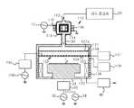
도 1에 도시된 바와 같이, 본 발명에 따른 플라즈마 반응기(100)는 플라즈마를 생성하여 공급하는 원격 플라즈마 발생기(110)와 내부에 방전 공간이 구비된 플라즈마 챔버(120) 및 플라즈마 가스의 온도를 상승시키기 위한 핫 배플판(150)으로 구성된다. 원격 플라즈마 발생기(110)로부터 제공받은 플라즈마 가스는 플라즈마 챔버(120) 내부에서 핫 배플판(150)에 의해 온도가 상승되어 피처리 기판(1)을 어닐링 처리한다.As shown in FIG. 1, the
원격 플라즈마 발생기(110)는 가스 입구(112)와 가스 출구(114)를 갖는 환형 방전관(111)과 환형 방전관(111)에 공통으로 결합되는 환형 코어(116)를 포함한다. 환형 코어(116)에는 전원 공급원(10)에 전기적으로 연결되는 코일(118)이 권선된다. 가스 공급원(20)으로부터 가스 입구(112)를 통해 환형 방전관(111) 내부로 제공된 가스는 환형 방전관(111) 내부에서 유도된 플라즈마에 의해 활성화되어 플라즈마 가스를 생성한다.The
플라즈마 챔버(120)는 원격 플라즈마 발생기(110)와 연결되어 플라즈마 가스를 제공받는다. 플라즈마 챔버(120)는 상부에 활성화된 플라즈마 가스를 제공받기 위한 개구부가 구비된다. 원격 플라즈마 발생기(110)의 환형 방전관(111)의 가스 출구(114)와 플라즈마 챔버(120)의 개구부는 어댑터(130)로 연결된다. 어댑터(130)는 환형 방전관(111)과 플라즈마 챔버(120) 사이를 절연하기 위한 절연구간이 포함된다. 플라즈마 챔버(120) 내부에는 피처리 기판(1)을 지지하기 위한 기판 지지대(124)를 포함한다. 피처리 기판(1)은 예를 들어, 반도체 장치, 디스플레이 장치, 태양전지 등과 같은 다양한 장치들의 제조를 위한 웨이퍼 기판, 유리 기판, 플라스틱 기판 등과 같은 기판들이다.The
기판 지지대(124)는 바이어스 전원 공급원(32, 34)에 연결되어 바이어스된다. 예를 들어, 서로 다른 무선 주파수 전원을 공급하는 두 개의 바이어스 전원 공급원(32, 34)이 임피던스 정합기(35)를 통하여 기판 지지대(124)에 전기적으로 연결되어 바이어스된다. 기판 지지대(124)의 이중 바이어스 구조는 플라즈마 반응기(100)의 내부에 플라즈마 발생을 용이하게 하고, 플라즈마 이온 에너지 조절을 더욱 개선시켜 공정 생산력을 향상시킬 수 있다. 또는 단일 바이어스 구조로 변형 실시할 수도 있다. 또는 기판 지지대(124)는 바이어스 전원의 공급 없이 제로 퍼텐셜(zero potential)을 갖는 구조로 변형 실시될 수도 있다. 그리고 기판 지지대(124)는 정전척을 포함할 수 있다. 또는 기판 지지대(124)는 히터를 포함할 수 있다.
플라즈마 챔버(120)의 내부 방전공간에는 활성화된 플라즈마 가스를 피처리 기판(1)에 균일하게 분배시키기 위한 가스 분배 배플(127)이 기판 지지대(124)의 상부에 구비된다. 가스 분배 배플(127)은 활성화된 가스가 통과할 수 있는 다수 개의 홀(127a)이 구비된다. 플라즈마 챔버(120) 내부로 유입된 플라즈마 가스는 가스 분배 배플(127)의 홀(127a)을 통과하면서 피처리 기판(1)에 균일하게 분배된다. 가스 분배 배플(127)은 세라믹 절연체 또는 메탈로 구성된다. 여기서 가스 분배 배플(127)은 핫 배플판(150)보다 상부에 구비될 수도 있고, 핫 배플판(150)과 기판 지지대(124) 사이에 구비될 수도 있다.In the internal discharge space of the
또한 플라즈마 챔버(120)의 하부에는 반응이 완료된 반응가스가 균일한 양으로 배기될 수 있도록 배기펌프(40)를 갖는 배기구조가 구비된다.In addition, the lower portion of the
핫 배플판(150)은 플라즈마 챔버(120) 내부에 구비되어 전원부(151)으로부터 전력을 제공받아 구동된다. 핫 배플판(150)은 플라즈마 챔버(120) 내부로 제공된 플라즈마 가스의 온도를 상승시킨다. 핫 배플판(150)의 구성에 대해서는 하기에서 상세하게 설명한다.
The
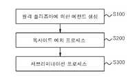
도 2는 본 발명의 바람직한 실시예에 따른 핫 배플판이 구비된 플라즈마 반응기를 이용한 처리 방법을 도시한 흐름도이다.2 is a flowchart illustrating a treatment method using a plasma reactor equipped with a hot baffle plate according to a preferred embodiment of the present invention.
도 2에 도시된 바와 같이, 플라즈마 반응기(100)를 이용하여 피처리 기판(1)을 처리하는 방법은 먼저, 상기에 설명한 구조를 갖는 원격 플라즈마 발생기(110)에서 플라즈마 가스를 발생시켜 플라즈마 챔버(120)로 공급한다. 이때 원격 플라즈마 발생기(110)에서는 피처리 기판(1)의 식각을 위한 에천트 가스를 발생시킨다(S100).As shown in FIG. 2, a method of treating a
원격 플라즈마 발생기(110)에서 발생된 에천트 가스는 플라즈마 챔버(120) 내부로 유입된다. 플라즈마 챔버(120)로 유입된 에천트 가스는 가스 분배 배플(127) 및 핫 배플판(150)에 의해 균일하게 피처리 기판(1)로 분배된다. 플라즈마 챔버(120) 내부의 에천트 가스를 이용하여 피처리 기판(1)의 옥사이드 에치 프로세스를 수행한다(S200).The etchant gas generated by the
옥사이드 에치 프로세스가 수행된 피처리 기판(1)은 서브리미네이션 프로세스이 수행된다. 즉, 핫 배플판(150)을 구동하면 핫 배플판(150)이 발열되면서 열을 발생한다. 발생된 열은 플라즈마 챔버(120) 내부에 포함된 에천트 가스의 온도를 상승시킴으로써 피처리 기판(1)을 어닐링 처리하여 서브리미네이션 프로세스가 수행된다(S300). The
옥사이드 에치 프로세스와 서브리미네이션 프로세스는 본 발명에 따른 플라즈마 챔버(120) 내부에서 순차적으로 수행된다.
The oxide etch process and the sublimation process are performed sequentially inside the
도 3은 본 발명의 바람직한 실시예에 따른 핫 배플판이 구비된 플라즈마 반응기의 핫 배플판을 도시한 평면도이다.Figure 3 is a plan view showing a hot baffle plate of the plasma reactor with a hot baffle plate according to a preferred embodiment of the present invention.
도 3에 도시된 바와 같이, 핫 배플판(150)은 히팅 플레이트(152)와 히팅 코일(154) 및 가스 분사홀(156)로 구성된다. 히팅 플레이트(152)는 판 형태로 기판 지지대(124)와 가스 분배 배플(127) 사이에 구비된다. 이때 히팅 플레이트(152)는 기판 지지대(124)와 평행하게 구비된다. 히팅 코일(154)은 히팅 플레이트(152)의 내부에 매설되어 전원부(151)으로부터 전력을 제공받아 구동된다. 이때, 히팅 코일(154)은 히팅 플레이트(152)에 나선형으로 권선되면서 매설되어 히팅 플레이트(152) 전 영역에 설치될 수 있도록 한다. 히팅 코일(154)은 전원부(151)으로부터 전력을 제공받으면 외부로 열을 발생시킨다. 히팅 코일(154)에서 발생된 열은 플라즈마 챔버(120) 내부에 유입된 플라즈마 가스의 온도를 상승시켜 피처리 기판(1)을 어닐링 처리한다.As shown in FIG. 3, the
가스 분사홀(156)은 히팅 플레이트(152)을 관통하여 다수 개가 구비된다. 가스 분사홀(156)은 히팅 플레이트(152) 전체 영역에 고르게 분포되어 플라즈마 챔버(120) 내부로 유입된 플라즈마 가스가 통과하면서 균일하게 피처리 기판(1)에 분배된다. 이때, 플라즈마 챔버(120) 내부에 가스 분배 배플(127)이 구비되어 있으면, 가스 분배 배플(127)에 의해 균일하게 분배된 플라즈마 가스가 다시 히팅 플레이트(152)에 의해 균일하게 분배될 수 있다.A plurality of gas injection holes 156 are provided through the
그러므로 핫 배플판(150)에서 발열된 열을 이용하여 어닐링 처리를 위한 고온의 플라즈마 가스가 생성될 수 있어 효율적인 피처리 기판(1) 어닐링 처리가 가능하다.Therefore, high temperature plasma gas for the annealing process can be generated using the heat generated from the
히팅 플레이트(152)는 알루미늄과 같은 도체 또는 석영과 같은 절연체로 구성될 수 있다. 히팅 플레이트(152)가 도체로 구성된 경우 히팅 플레이트(152)에 무선 주파수 전원을 공급하는 전원 공급원(200)을 연결하여 히팅 플레이트(152)를 상부 전극으로 사용할 수 있다. 히팅 플레이트(152)는 전원 공급원(200)으로부터 임피던스 정합기(210)를 통하여 무선 주파수 전원을 공급받는다. 그러므로 히팅 플레이트(152)와 기판 지지대(124) 사이에서 방전되면서 플라즈마 챔버(120) 내부로 제공된 플라즈마 가스를 다시 이온화한다.The
이때, 히팅 플레이트(152)로 공급된 무선 주파수 전원이 히팅 코일(154)로 유입되는 것을 방지하기 위하여 히팅 코일(154)에 필터부(157)를 연결한다. 히팅 플레이트(152)로 공급된 무선 주파수가 히팅 코일(154)로 유입되면 히팅 플레이트(152)와 기판 지지대(124) 사이에서 방전이 발생되지 않는다. 그러므로 히팅 코일(154)에 무선 주파수를 차단하기 위한 필터부(157)를 연결한다.In this case, the
도 4 및 도 5는 도 3에 도시된 핫 배플판의 단면을 도시한 단면도이다.4 and 5 are cross-sectional views showing a cross section of the hot baffle plate shown in FIG.
도 4 및 도 5에 도시된 바와 같이, 히팅 플레이트(152)는 상부 플레이트(152a)와 하부 플레이트(152b)가 결합되어 형성될 수 있다. 이때, 상부 플레이트(152a)와 하부 플레이트(152b) 사이에 히팅 코일(154)이 설치된다.As shown in FIGS. 4 and 5, the
도 4에 도시된 바와 같이, 히팅 플레이트(152)가 도체로 구성된 경우 히팅 플레이트(152)와 히팅 코일(154) 사이를 절연시키기 위한 절연커버(155)를 구비할 수 있다. 절연커버(155)는 히팅 코일(152)의 외부를 감싸도록 구비되어 히팅 플레이트(152)와 히팅 코일(154)이 절연되도록 한다.As shown in FIG. 4, when the
또한 도 5에 도시된 바와 같이, 히팅 플레이트(152)가 절연체로 구성된 경우에는 바로 히팅 플레이트(152) 내부에 히팅 코일(154)을 매설할 수도 있다.In addition, as shown in FIG. 5, when the
도 6은 본 발명의 또 다른 실시예에 따른 핫 배플판이 구비된 플라즈마 반응기의 핫 배플판을 도시한 평면도이다.6 is a plan view illustrating a hot baffle plate of the plasma reactor with a hot baffle plate according to another embodiment of the present invention.
도 6에 도시된 바와 같이, 핫 배플판(150a)은 히팅 플레이트(152)의 테두리 영역으로 히팅 코일(154a)이 구비될 수 있다. 즉, 도 3에 도시된 바와 같이, 히팅 코일(154)이 나선형으로 권선될 수도 있고, 히팅 코일(154a)이 히팅 플레이트(152)의 중심 영역 또는 테두리 영역에 권선되어 설치될 수도 있다. 여기에서도 히팅 플레이트(152)가 도체인 경우에는 임피던스 정합기(210)와 전원 공급원(200)이 연결되어 무선 주파수 전원을 제공받을 수 있다.As illustrated in FIG. 6, the
도 7은 본 발명의 바람직한 제2 실시예에 따른 핫 배플판이 구비된 플라즈마 반응기를 도시한 단면도이다.7 is a cross-sectional view showing a plasma reactor with a hot baffle plate according to a second embodiment of the present invention.
도 7에 도시된 바와 같이, 핫 배플판(150)의 히팅 플레이트(152)를 이용하여 플라즈마 가스를 균일하게 분배할 수도 있다. 즉, 플라즈마 챔버(120) 내부에 가스 분배 배플을 별도로 설치하지 않고, 히팅 플레이트(152)에 구비된 다수 개의 분사홀(156)을 통해 플라즈마 가스가 피처리 기판(1)에 균일하게 분배되도록 한다.
As illustrated in FIG. 7, the plasma gas may be uniformly distributed using the
도 8은 본 발명의 바람직한 제3 실시예에 따른 핫 배플판이 구비된 플라즈마 반응기를 도시한 단면도이다.8 is a cross-sectional view showing a plasma reactor with a hot baffle plate according to a third embodiment of the present invention.
도 8에 도시된 바와 같이, 플라즈마 챔버(120)의 내부에 챔버 히팅선(126)을 설치할 수 있다. 챔버 히팅선(126)은 전원부(128)로부터 전력을 공급받아 발열된다. 챔버 히팅선(126)에서 발생된 열은 플라즈마 챔버(120) 내부의 온도를 상승시켜 공정 진행 시 발생되는 챔버 오염을 미연에 방지한다.
As shown in FIG. 8, the
이상에서 설명된 본 발명의 배플판이 구비된 플라즈마 반응기 및 이를 이용한 기판 처리 방법의 실시예는 예시적인 것에 불과하며, 본 발명이 속한 기술분야의 통상의 지식을 가진 자라면 이로부터 다양한 변형 및 균등한 타 실시예가 가능하다는 점을 잘 알 수 있을 것이다. 그럼으로 본 발명은 상기의 상세한 설명에서 언급되는 형태로만 한정되는 것은 아님을 잘 이해할 수 있을 것이다. 따라서 본 발명의 진정한 기술적 보호 범위는 첨부된 특허청구범위의 기술적 사상에 의해 정해져야 할 것이다. 또한, 본 발명은 첨부된 청구범위에 의해 정의되는 본 발명의 정신과 그 범위 내에 있는 모든 변형물과 균등물 및 대체물을 포함하는 것으로 이해되어야 한다.The embodiment of the plasma reactor equipped with the baffle plate of the present invention described above and the substrate processing method using the same are merely exemplary, and those skilled in the art to which the present invention pertains various modifications and equivalents therefrom. It will be appreciated that other embodiments are possible. Accordingly, it is to be understood that the present invention is not limited to the above-described embodiments. Accordingly, the true scope of the present invention should be determined by the technical idea of the appended claims. It is also to be understood that the invention includes all modifications, equivalents, and alternatives falling within the spirit and scope of the invention as defined by the appended claims.
1: 피처리 기판 10, 200: 전원 공급원
20: 가스 공급원 32, 34: 바이어스 전원 공급원
35, 210: 임피던스 정합기 40: 배기 펌프
100: 플라즈마 반응기 110: 원격 플라즈마 발생기
111: 환형 방전관 112: 가스 입구
114: 가스 출구 116: 환형 코어
118: 코일 120: 플라즈마 챔버
124: 기판 지지대 126: 챔버 히팅선
127: 가스 분배 배플 127a: 홀
130: 어댑터 150, 150a: 핫 배플판
151, 128: 전원부 152: 히팅 플레이트
152a, 152b: 상,하부 플레이트 154, 154a: 히팅 코일
155: 절연 커버 156: 가스 분사홀1: substrate to be processed 10, 200: power source
20:
35, 210: impedance matcher 40: exhaust pump
100: plasma reactor 110: remote plasma generator
111: annular discharge tube 112: gas inlet
114: gas outlet 116: annular core
118: coil 120: plasma chamber
124: substrate support 126: chamber heating line
127:
130:
151 and 128: power supply 152: heating plate
152a and 152b: upper and
155: insulation cover 156: gas injection hole
Claims (15)
Translated fromKorean상기 플라즈마 챔버 내부의 방전공간에 구비되는 도체의 히팅 플레이트와 상기 히팅 플레이트에 구비되어 히터 전원으로부터 전력을 공급받아 발열되는 히팅 코일 및 상기 플라즈마 챔버 내부의 플라즈마가 통과할 수 있도록 구비된 다수 개의 가스 분사홀을 구비하는 핫 배플판;
상기 히팅 플레이트에 연결되어 상기 히팅 플레이트로 무선 주파수 전원을 제공하는 전원 공급원; 및
상기 전원 공급원과 상기 히팅 플레이트 사이에 구비되어 임피던스 정합을 수행하는 임피던스 정합기를 포함하는 것을 특징으로 하는 핫 배플판이 구비된 플라즈마 반응기.A plasma chamber provided with a substrate support for supporting a plasma discharge space and a substrate to be processed;
Heating plates of the conductors provided in the discharge space inside the plasma chamber and heating coils provided in the heating plates to generate heat by receiving power from a heater power source, and a plurality of gas injections provided to allow the plasma inside the plasma chamber to pass therethrough. A hot baffle plate having a hole;
A power supply connected to the heating plate to provide radio frequency power to the heating plate; And
And a impedance matcher provided between the power supply source and the heating plate to perform impedance matching.
상기 플라즈마 챔버 내부로 플라즈마를 제공하기 위한 원격 플라즈마 발생기를 포함하는 것을 특징으로 하는 핫 배플판이 구비된 플라즈마 반응기.The method of claim 1,
And a remote plasma generator for providing plasma into the plasma chamber.
상기 원격 플라즈마 발생기는
가스 입구와 가스 출구를 갖는 환형 방전관; 및
상기 환형 방전관에 공통으로 결합되어 전원 공급원에 전기적으로 연결되는 코일이 권선된 환형 코어를 포함하는 것을 특징으로 하는 핫 배플판이 구비된 플라즈마 반응기.The method of claim 2,
The remote plasma generator
An annular discharge tube having a gas inlet and a gas outlet; And
And a annular core wound around a coil coupled to the annular discharge tube and electrically connected to a power supply source.
상기 히팅 코일의 외부를 감싸도록 구비된 절연커버를 포함하는 것을 특징으로 하는 핫 배플판이 구비된 플라즈마 반응기.The method of claim 1,
Plasma reactor with a hot baffle plate, characterized in that it comprises an insulating cover provided to surround the outside of the heating coil.
상기 히팅 코일에 연결되어 상기 히팅 플레이트에 제공되는 무선 주파수가 상기 히팅 코일로 유입되는 것을 방지하기 위한 필터부를 포함하는 것을 특징으로 하는 핫 배플판이 구비된 플라즈마 반응기.The method of claim 1,
And a filter unit connected to the heating coil to prevent a radio frequency provided to the heating plate from being introduced into the heating coil.
상기 플라즈마 챔버는 상기 플라즈마를 내부의 플라즈마가 균일하게 상기 피처리 기판으로 분배되도록 하기 위한 가스 분배 배플을 포함하는 것을 특징으로 하는 핫 배플판이 구비된 플라즈마 반응기.The method of claim 1,
And the plasma chamber includes a gas distribution baffle for causing the plasma to be uniformly distributed therein to the target substrate.
상기 플라즈마 챔버는 히팅 전원으로부터 전력을 제공받아 발열되는 챔버 히팅선을 포함하는 것을 특징으로 하는 핫 배플판이 구비된 플라즈마 반응기.The method of claim 1,
The plasma chamber is a plasma reactor having a hot baffle plate, characterized in that it comprises a chamber heating line that generates heat by receiving power from a heating power source.
상기 원격 플라즈마 발생기는 에천트 가스를 발생하여 상기 플라즈마 챔버 내부로 공급하는 것을 특징으로 하는 핫 배플판이 구비된 플라즈마 반응기.The method of claim 3,
The remote plasma generator is a plasma reactor with a hot baffle plate, characterized in that for generating an etchant gas into the plasma chamber.
에천트 가스를 생성하는 단계;
상기 에천트 가스를 통해 피처리 기판을 에칭하는 단계; 및
상기 에칭된 피처리 기판에 플라즈마 챔버 내부에 구비된 핫 배플판을 이용하여 서브리미네이션을 수행하는 단계를 포함하는 것을 특징으로 하는 핫 배플판이 구비된 플라즈마 반응기를 이용한 기판 처리 방법.A plasma chamber provided with a substrate support for supporting a plasma discharge space and a substrate to be processed; Heating plates of the conductors provided in the discharge space inside the plasma chamber and heating coils provided in the heating plates to generate heat by receiving power from a heater power source, and a plurality of gas injections provided to allow the plasma inside the plasma chamber to pass therethrough. A hot baffle plate having a hole; A power supply connected to the heating plate to provide radio frequency power to the heating plate; In the substrate processing method using a plasma reactor provided with a hot baffle plate comprising an impedance matching device provided between the power supply and the heating plate for performing impedance matching,
Generating an etchant gas;
Etching the substrate to be processed through the etchant gas; And
And performing a sublimation on the etched substrate by using a hot baffle plate provided in the plasma chamber.
상기 플라즈마 반응기는 원격 플라즈마 발생기를 더 포함하고,
상기 에천트 가스 생성 단계에서 상기 에천트 가스는 상기 원격 플라즈마 발생기를 통해 생성되는 것을 특징으로 하는 핫 배플판이 구비된 플라즈마 반응기를 이용한 기판 처리 방법.The method of claim 12,
The plasma reactor further comprises a remote plasma generator,
In the etchant gas generation step, the etchant gas is generated by the remote plasma generator, characterized in that the substrate processing method using a plasma reactor with a hot baffle plate.
Priority Applications (1)
| Application Number | Priority Date | Filing Date | Title |
|---|---|---|---|
| KR1020110029329AKR101200720B1 (en) | 2011-03-31 | 2011-03-31 | Plasma reactor having hot baffle and wafer handle method thereof |
Applications Claiming Priority (1)
| Application Number | Priority Date | Filing Date | Title |
|---|---|---|---|
| KR1020110029329AKR101200720B1 (en) | 2011-03-31 | 2011-03-31 | Plasma reactor having hot baffle and wafer handle method thereof |
Publications (2)
| Publication Number | Publication Date |
|---|---|
| KR20120111060A KR20120111060A (en) | 2012-10-10 |
| KR101200720B1true KR101200720B1 (en) | 2012-11-13 |
Family
ID=47281810
Family Applications (1)
| Application Number | Title | Priority Date | Filing Date |
|---|---|---|---|
| KR1020110029329AActiveKR101200720B1 (en) | 2011-03-31 | 2011-03-31 | Plasma reactor having hot baffle and wafer handle method thereof |
Country Status (1)
| Country | Link |
|---|---|
| KR (1) | KR101200720B1 (en) |
Families Citing this family (304)
| Publication number | Priority date | Publication date | Assignee | Title |
|---|---|---|---|---|
| US9394608B2 (en) | 2009-04-06 | 2016-07-19 | Asm America, Inc. | Semiconductor processing reactor and components thereof |
| US8802201B2 (en) | 2009-08-14 | 2014-08-12 | Asm America, Inc. | Systems and methods for thin-film deposition of metal oxides using excited nitrogen-oxygen species |
| US20130023129A1 (en) | 2011-07-20 | 2013-01-24 | Asm America, Inc. | Pressure transmitter for a semiconductor processing environment |
| US9017481B1 (en) | 2011-10-28 | 2015-04-28 | Asm America, Inc. | Process feed management for semiconductor substrate processing |
| US10714315B2 (en) | 2012-10-12 | 2020-07-14 | Asm Ip Holdings B.V. | Semiconductor reaction chamber showerhead |
| US20160376700A1 (en) | 2013-02-01 | 2016-12-29 | Asm Ip Holding B.V. | System for treatment of deposition reactor |
| US9484191B2 (en)* | 2013-03-08 | 2016-11-01 | Asm Ip Holding B.V. | Pulsed remote plasma method and system |
| US11015245B2 (en) | 2014-03-19 | 2021-05-25 | Asm Ip Holding B.V. | Gas-phase reactor and system having exhaust plenum and components thereof |
| US10858737B2 (en) | 2014-07-28 | 2020-12-08 | Asm Ip Holding B.V. | Showerhead assembly and components thereof |
| US9890456B2 (en) | 2014-08-21 | 2018-02-13 | Asm Ip Holding B.V. | Method and system for in situ formation of gas-phase compounds |
| US10941490B2 (en) | 2014-10-07 | 2021-03-09 | Asm Ip Holding B.V. | Multiple temperature range susceptor, assembly, reactor and system including the susceptor, and methods of using the same |
| US10276355B2 (en) | 2015-03-12 | 2019-04-30 | Asm Ip Holding B.V. | Multi-zone reactor, system including the reactor, and method of using the same |
| US10458018B2 (en) | 2015-06-26 | 2019-10-29 | Asm Ip Holding B.V. | Structures including metal carbide material, devices including the structures, and methods of forming same |
| US10211308B2 (en) | 2015-10-21 | 2019-02-19 | Asm Ip Holding B.V. | NbMC layers |
| US11139308B2 (en) | 2015-12-29 | 2021-10-05 | Asm Ip Holding B.V. | Atomic layer deposition of III-V compounds to form V-NAND devices |
| US10529554B2 (en) | 2016-02-19 | 2020-01-07 | Asm Ip Holding B.V. | Method for forming silicon nitride film selectively on sidewalls or flat surfaces of trenches |
| US10343920B2 (en) | 2016-03-18 | 2019-07-09 | Asm Ip Holding B.V. | Aligned carbon nanotubes |
| US10190213B2 (en) | 2016-04-21 | 2019-01-29 | Asm Ip Holding B.V. | Deposition of metal borides |
| US10865475B2 (en) | 2016-04-21 | 2020-12-15 | Asm Ip Holding B.V. | Deposition of metal borides and silicides |
| US10367080B2 (en) | 2016-05-02 | 2019-07-30 | Asm Ip Holding B.V. | Method of forming a germanium oxynitride film |
| US11453943B2 (en) | 2016-05-25 | 2022-09-27 | Asm Ip Holding B.V. | Method for forming carbon-containing silicon/metal oxide or nitride film by ALD using silicon precursor and hydrocarbon precursor |
| US10612137B2 (en) | 2016-07-08 | 2020-04-07 | Asm Ip Holdings B.V. | Organic reactants for atomic layer deposition |
| US9859151B1 (en) | 2016-07-08 | 2018-01-02 | Asm Ip Holding B.V. | Selective film deposition method to form air gaps |
| US10714385B2 (en) | 2016-07-19 | 2020-07-14 | Asm Ip Holding B.V. | Selective deposition of tungsten |
| US9887082B1 (en) | 2016-07-28 | 2018-02-06 | Asm Ip Holding B.V. | Method and apparatus for filling a gap |
| KR102532607B1 (en) | 2016-07-28 | 2023-05-15 | 에이에스엠 아이피 홀딩 비.브이. | Substrate processing apparatus and method of operating the same |
| US9812320B1 (en) | 2016-07-28 | 2017-11-07 | Asm Ip Holding B.V. | Method and apparatus for filling a gap |
| US10643826B2 (en) | 2016-10-26 | 2020-05-05 | Asm Ip Holdings B.V. | Methods for thermally calibrating reaction chambers |
| US11532757B2 (en) | 2016-10-27 | 2022-12-20 | Asm Ip Holding B.V. | Deposition of charge trapping layers |
| US10229833B2 (en) | 2016-11-01 | 2019-03-12 | Asm Ip Holding B.V. | Methods for forming a transition metal nitride film on a substrate by atomic layer deposition and related semiconductor device structures |
| US10714350B2 (en) | 2016-11-01 | 2020-07-14 | ASM IP Holdings, B.V. | Methods for forming a transition metal niobium nitride film on a substrate by atomic layer deposition and related semiconductor device structures |
| KR102546317B1 (en) | 2016-11-15 | 2023-06-21 | 에이에스엠 아이피 홀딩 비.브이. | Gas supply unit and substrate processing apparatus including the same |
| KR102762543B1 (en) | 2016-12-14 | 2025-02-05 | 에이에스엠 아이피 홀딩 비.브이. | Substrate processing apparatus |
| US11581186B2 (en) | 2016-12-15 | 2023-02-14 | Asm Ip Holding B.V. | Sequential infiltration synthesis apparatus |
| US11447861B2 (en) | 2016-12-15 | 2022-09-20 | Asm Ip Holding B.V. | Sequential infiltration synthesis apparatus and a method of forming a patterned structure |
| KR102700194B1 (en) | 2016-12-19 | 2024-08-28 | 에이에스엠 아이피 홀딩 비.브이. | Substrate processing apparatus |
| US10269558B2 (en) | 2016-12-22 | 2019-04-23 | Asm Ip Holding B.V. | Method of forming a structure on a substrate |
| US10867788B2 (en) | 2016-12-28 | 2020-12-15 | Asm Ip Holding B.V. | Method of forming a structure on a substrate |
| US11390950B2 (en) | 2017-01-10 | 2022-07-19 | Asm Ip Holding B.V. | Reactor system and method to reduce residue buildup during a film deposition process |
| US10468261B2 (en) | 2017-02-15 | 2019-11-05 | Asm Ip Holding B.V. | Methods for forming a metallic film on a substrate by cyclical deposition and related semiconductor device structures |
| US10529563B2 (en) | 2017-03-29 | 2020-01-07 | Asm Ip Holdings B.V. | Method for forming doped metal oxide films on a substrate by cyclical deposition and related semiconductor device structures |
| KR102457289B1 (en) | 2017-04-25 | 2022-10-21 | 에이에스엠 아이피 홀딩 비.브이. | Method for depositing a thin film and manufacturing a semiconductor device |
| US10892156B2 (en) | 2017-05-08 | 2021-01-12 | Asm Ip Holding B.V. | Methods for forming a silicon nitride film on a substrate and related semiconductor device structures |
| US10770286B2 (en) | 2017-05-08 | 2020-09-08 | Asm Ip Holdings B.V. | Methods for selectively forming a silicon nitride film on a substrate and related semiconductor device structures |
| US10886123B2 (en) | 2017-06-02 | 2021-01-05 | Asm Ip Holding B.V. | Methods for forming low temperature semiconductor layers and related semiconductor device structures |
| US12040200B2 (en) | 2017-06-20 | 2024-07-16 | Asm Ip Holding B.V. | Semiconductor processing apparatus and methods for calibrating a semiconductor processing apparatus |
| US11306395B2 (en) | 2017-06-28 | 2022-04-19 | Asm Ip Holding B.V. | Methods for depositing a transition metal nitride film on a substrate by atomic layer deposition and related deposition apparatus |
| US10685834B2 (en) | 2017-07-05 | 2020-06-16 | Asm Ip Holdings B.V. | Methods for forming a silicon germanium tin layer and related semiconductor device structures |
| KR20190009245A (en) | 2017-07-18 | 2019-01-28 | 에이에스엠 아이피 홀딩 비.브이. | Methods for forming a semiconductor device structure and related semiconductor device structures |
| US10541333B2 (en) | 2017-07-19 | 2020-01-21 | Asm Ip Holding B.V. | Method for depositing a group IV semiconductor and related semiconductor device structures |
| US11018002B2 (en) | 2017-07-19 | 2021-05-25 | Asm Ip Holding B.V. | Method for selectively depositing a Group IV semiconductor and related semiconductor device structures |
| US11374112B2 (en) | 2017-07-19 | 2022-06-28 | Asm Ip Holding B.V. | Method for depositing a group IV semiconductor and related semiconductor device structures |
| US10590535B2 (en) | 2017-07-26 | 2020-03-17 | Asm Ip Holdings B.V. | Chemical treatment, deposition and/or infiltration apparatus and method for using the same |
| TWI815813B (en) | 2017-08-04 | 2023-09-21 | 荷蘭商Asm智慧財產控股公司 | Showerhead assembly for distributing a gas within a reaction chamber |
| US10770336B2 (en) | 2017-08-08 | 2020-09-08 | Asm Ip Holding B.V. | Substrate lift mechanism and reactor including same |
| US10692741B2 (en) | 2017-08-08 | 2020-06-23 | Asm Ip Holdings B.V. | Radiation shield |
| US11769682B2 (en) | 2017-08-09 | 2023-09-26 | Asm Ip Holding B.V. | Storage apparatus for storing cassettes for substrates and processing apparatus equipped therewith |
| US11139191B2 (en) | 2017-08-09 | 2021-10-05 | Asm Ip Holding B.V. | Storage apparatus for storing cassettes for substrates and processing apparatus equipped therewith |
| US11830730B2 (en) | 2017-08-29 | 2023-11-28 | Asm Ip Holding B.V. | Layer forming method and apparatus |
| KR102491945B1 (en) | 2017-08-30 | 2023-01-26 | 에이에스엠 아이피 홀딩 비.브이. | Substrate processing apparatus |
| US11295980B2 (en) | 2017-08-30 | 2022-04-05 | Asm Ip Holding B.V. | Methods for depositing a molybdenum metal film over a dielectric surface of a substrate by a cyclical deposition process and related semiconductor device structures |
| US11056344B2 (en) | 2017-08-30 | 2021-07-06 | Asm Ip Holding B.V. | Layer forming method |
| KR102401446B1 (en) | 2017-08-31 | 2022-05-24 | 에이에스엠 아이피 홀딩 비.브이. | Substrate processing apparatus |
| KR102630301B1 (en) | 2017-09-21 | 2024-01-29 | 에이에스엠 아이피 홀딩 비.브이. | Method of sequential infiltration synthesis treatment of infiltrateable material and structures and devices formed using same |
| US10844484B2 (en) | 2017-09-22 | 2020-11-24 | Asm Ip Holding B.V. | Apparatus for dispensing a vapor phase reactant to a reaction chamber and related methods |
| US10658205B2 (en) | 2017-09-28 | 2020-05-19 | Asm Ip Holdings B.V. | Chemical dispensing apparatus and methods for dispensing a chemical to a reaction chamber |
| US10403504B2 (en) | 2017-10-05 | 2019-09-03 | Asm Ip Holding B.V. | Method for selectively depositing a metallic film on a substrate |
| US10319588B2 (en) | 2017-10-10 | 2019-06-11 | Asm Ip Holding B.V. | Method for depositing a metal chalcogenide on a substrate by cyclical deposition |
| US10923344B2 (en) | 2017-10-30 | 2021-02-16 | Asm Ip Holding B.V. | Methods for forming a semiconductor structure and related semiconductor structures |
| US10910262B2 (en) | 2017-11-16 | 2021-02-02 | Asm Ip Holding B.V. | Method of selectively depositing a capping layer structure on a semiconductor device structure |
| US11022879B2 (en) | 2017-11-24 | 2021-06-01 | Asm Ip Holding B.V. | Method of forming an enhanced unexposed photoresist layer |
| WO2019103613A1 (en) | 2017-11-27 | 2019-05-31 | Asm Ip Holding B.V. | A storage device for storing wafer cassettes for use with a batch furnace |
| CN111344522B (en) | 2017-11-27 | 2022-04-12 | 阿斯莫Ip控股公司 | Including clean mini-environment device |
| US10872771B2 (en) | 2018-01-16 | 2020-12-22 | Asm Ip Holding B. V. | Method for depositing a material film on a substrate within a reaction chamber by a cyclical deposition process and related device structures |
| TWI799494B (en) | 2018-01-19 | 2023-04-21 | 荷蘭商Asm 智慧財產控股公司 | Deposition method |
| KR102695659B1 (en) | 2018-01-19 | 2024-08-14 | 에이에스엠 아이피 홀딩 비.브이. | Method for depositing a gap filling layer by plasma assisted deposition |
| US11018047B2 (en) | 2018-01-25 | 2021-05-25 | Asm Ip Holding B.V. | Hybrid lift pin |
| USD880437S1 (en) | 2018-02-01 | 2020-04-07 | Asm Ip Holding B.V. | Gas supply plate for semiconductor manufacturing apparatus |
| US11081345B2 (en) | 2018-02-06 | 2021-08-03 | Asm Ip Holding B.V. | Method of post-deposition treatment for silicon oxide film |
| US10896820B2 (en) | 2018-02-14 | 2021-01-19 | Asm Ip Holding B.V. | Method for depositing a ruthenium-containing film on a substrate by a cyclical deposition process |
| WO2019158960A1 (en) | 2018-02-14 | 2019-08-22 | Asm Ip Holding B.V. | A method for depositing a ruthenium-containing film on a substrate by a cyclical deposition process |
| US10731249B2 (en) | 2018-02-15 | 2020-08-04 | Asm Ip Holding B.V. | Method of forming a transition metal containing film on a substrate by a cyclical deposition process, a method for supplying a transition metal halide compound to a reaction chamber, and related vapor deposition apparatus |
| KR102636427B1 (en) | 2018-02-20 | 2024-02-13 | 에이에스엠 아이피 홀딩 비.브이. | Substrate processing method and apparatus |
| US10975470B2 (en) | 2018-02-23 | 2021-04-13 | Asm Ip Holding B.V. | Apparatus for detecting or monitoring for a chemical precursor in a high temperature environment |
| US11473195B2 (en) | 2018-03-01 | 2022-10-18 | Asm Ip Holding B.V. | Semiconductor processing apparatus and a method for processing a substrate |
| US11629406B2 (en) | 2018-03-09 | 2023-04-18 | Asm Ip Holding B.V. | Semiconductor processing apparatus comprising one or more pyrometers for measuring a temperature of a substrate during transfer of the substrate |
| US11114283B2 (en) | 2018-03-16 | 2021-09-07 | Asm Ip Holding B.V. | Reactor, system including the reactor, and methods of manufacturing and using same |
| KR102646467B1 (en) | 2018-03-27 | 2024-03-11 | 에이에스엠 아이피 홀딩 비.브이. | Method of forming an electrode on a substrate and a semiconductor device structure including an electrode |
| US11230766B2 (en) | 2018-03-29 | 2022-01-25 | Asm Ip Holding B.V. | Substrate processing apparatus and method |
| US11088002B2 (en) | 2018-03-29 | 2021-08-10 | Asm Ip Holding B.V. | Substrate rack and a substrate processing system and method |
| KR102501472B1 (en) | 2018-03-30 | 2023-02-20 | 에이에스엠 아이피 홀딩 비.브이. | Substrate processing method |
| KR102600229B1 (en) | 2018-04-09 | 2023-11-10 | 에이에스엠 아이피 홀딩 비.브이. | Substrate supporting device, substrate processing apparatus including the same and substrate processing method |
| TWI811348B (en) | 2018-05-08 | 2023-08-11 | 荷蘭商Asm 智慧財產控股公司 | Methods for depositing an oxide film on a substrate by a cyclical deposition process and related device structures |
| US12025484B2 (en) | 2018-05-08 | 2024-07-02 | Asm Ip Holding B.V. | Thin film forming method |
| US12272527B2 (en) | 2018-05-09 | 2025-04-08 | Asm Ip Holding B.V. | Apparatus for use with hydrogen radicals and method of using same |
| KR20190129718A (en) | 2018-05-11 | 2019-11-20 | 에이에스엠 아이피 홀딩 비.브이. | Methods for forming a doped metal carbide film on a substrate and related semiconductor device structures |
| KR102596988B1 (en) | 2018-05-28 | 2023-10-31 | 에이에스엠 아이피 홀딩 비.브이. | Method of processing a substrate and a device manufactured by the same |
| US11718913B2 (en) | 2018-06-04 | 2023-08-08 | Asm Ip Holding B.V. | Gas distribution system and reactor system including same |
| TWI840362B (en) | 2018-06-04 | 2024-05-01 | 荷蘭商Asm Ip私人控股有限公司 | Wafer handling chamber with moisture reduction |
| US11286562B2 (en) | 2018-06-08 | 2022-03-29 | Asm Ip Holding B.V. | Gas-phase chemical reactor and method of using same |
| KR102568797B1 (en) | 2018-06-21 | 2023-08-21 | 에이에스엠 아이피 홀딩 비.브이. | Substrate processing system |
| US10797133B2 (en) | 2018-06-21 | 2020-10-06 | Asm Ip Holding B.V. | Method for depositing a phosphorus doped silicon arsenide film and related semiconductor device structures |
| TWI873894B (en) | 2018-06-27 | 2025-02-21 | 荷蘭商Asm Ip私人控股有限公司 | Cyclic deposition methods for forming metal-containing material and films and structures including the metal-containing material |
| KR102854019B1 (en) | 2018-06-27 | 2025-09-02 | 에이에스엠 아이피 홀딩 비.브이. | Periodic deposition method for forming a metal-containing material and films and structures comprising the metal-containing material |
| US10612136B2 (en) | 2018-06-29 | 2020-04-07 | ASM IP Holding, B.V. | Temperature-controlled flange and reactor system including same |
| KR102686758B1 (en) | 2018-06-29 | 2024-07-18 | 에이에스엠 아이피 홀딩 비.브이. | Method for depositing a thin film and manufacturing a semiconductor device |
| US10388513B1 (en) | 2018-07-03 | 2019-08-20 | Asm Ip Holding B.V. | Method for depositing silicon-free carbon-containing film as gap-fill layer by pulse plasma-assisted deposition |
| US10755922B2 (en) | 2018-07-03 | 2020-08-25 | Asm Ip Holding B.V. | Method for depositing silicon-free carbon-containing film as gap-fill layer by pulse plasma-assisted deposition |
| US10767789B2 (en) | 2018-07-16 | 2020-09-08 | Asm Ip Holding B.V. | Diaphragm valves, valve components, and methods for forming valve components |
| US11053591B2 (en) | 2018-08-06 | 2021-07-06 | Asm Ip Holding B.V. | Multi-port gas injection system and reactor system including same |
| US10883175B2 (en) | 2018-08-09 | 2021-01-05 | Asm Ip Holding B.V. | Vertical furnace for processing substrates and a liner for use therein |
| US10829852B2 (en) | 2018-08-16 | 2020-11-10 | Asm Ip Holding B.V. | Gas distribution device for a wafer processing apparatus |
| US11430674B2 (en) | 2018-08-22 | 2022-08-30 | Asm Ip Holding B.V. | Sensor array, apparatus for dispensing a vapor phase reactant to a reaction chamber and related methods |
| US11024523B2 (en) | 2018-09-11 | 2021-06-01 | Asm Ip Holding B.V. | Substrate processing apparatus and method |
| KR102707956B1 (en) | 2018-09-11 | 2024-09-19 | 에이에스엠 아이피 홀딩 비.브이. | Method for deposition of a thin film |
| US11049751B2 (en) | 2018-09-14 | 2021-06-29 | Asm Ip Holding B.V. | Cassette supply system to store and handle cassettes and processing apparatus equipped therewith |
| CN110970344B (en) | 2018-10-01 | 2024-10-25 | Asmip控股有限公司 | Substrate holding apparatus, system comprising the same and method of using the same |
| US11232963B2 (en) | 2018-10-03 | 2022-01-25 | Asm Ip Holding B.V. | Substrate processing apparatus and method |
| KR102592699B1 (en) | 2018-10-08 | 2023-10-23 | 에이에스엠 아이피 홀딩 비.브이. | Substrate support unit and apparatuses for depositing thin film and processing the substrate including the same |
| US10847365B2 (en) | 2018-10-11 | 2020-11-24 | Asm Ip Holding B.V. | Method of forming conformal silicon carbide film by cyclic CVD |
| US10811256B2 (en) | 2018-10-16 | 2020-10-20 | Asm Ip Holding B.V. | Method for etching a carbon-containing feature |
| KR102546322B1 (en) | 2018-10-19 | 2023-06-21 | 에이에스엠 아이피 홀딩 비.브이. | Substrate processing apparatus and substrate processing method |
| KR102605121B1 (en) | 2018-10-19 | 2023-11-23 | 에이에스엠 아이피 홀딩 비.브이. | Substrate processing apparatus and substrate processing method |
| USD948463S1 (en) | 2018-10-24 | 2022-04-12 | Asm Ip Holding B.V. | Susceptor for semiconductor substrate supporting apparatus |
| US12378665B2 (en) | 2018-10-26 | 2025-08-05 | Asm Ip Holding B.V. | High temperature coatings for a preclean and etch apparatus and related methods |
| US11087997B2 (en) | 2018-10-31 | 2021-08-10 | Asm Ip Holding B.V. | Substrate processing apparatus for processing substrates |
| KR102748291B1 (en) | 2018-11-02 | 2024-12-31 | 에이에스엠 아이피 홀딩 비.브이. | Substrate support unit and substrate processing apparatus including the same |
| US11572620B2 (en) | 2018-11-06 | 2023-02-07 | Asm Ip Holding B.V. | Methods for selectively depositing an amorphous silicon film on a substrate |
| US11031242B2 (en) | 2018-11-07 | 2021-06-08 | Asm Ip Holding B.V. | Methods for depositing a boron doped silicon germanium film |
| US10847366B2 (en) | 2018-11-16 | 2020-11-24 | Asm Ip Holding B.V. | Methods for depositing a transition metal chalcogenide film on a substrate by a cyclical deposition process |
| US10818758B2 (en) | 2018-11-16 | 2020-10-27 | Asm Ip Holding B.V. | Methods for forming a metal silicate film on a substrate in a reaction chamber and related semiconductor device structures |
| US12040199B2 (en) | 2018-11-28 | 2024-07-16 | Asm Ip Holding B.V. | Substrate processing apparatus for processing substrates |
| US11217444B2 (en) | 2018-11-30 | 2022-01-04 | Asm Ip Holding B.V. | Method for forming an ultraviolet radiation responsive metal oxide-containing film |
| KR102636428B1 (en) | 2018-12-04 | 2024-02-13 | 에이에스엠 아이피 홀딩 비.브이. | A method for cleaning a substrate processing apparatus |
| US11158513B2 (en) | 2018-12-13 | 2021-10-26 | Asm Ip Holding B.V. | Methods for forming a rhenium-containing film on a substrate by a cyclical deposition process and related semiconductor device structures |
| TWI874340B (en) | 2018-12-14 | 2025-03-01 | 荷蘭商Asm Ip私人控股有限公司 | Method of forming device structure, structure formed by the method and system for performing the method |
| TWI866480B (en) | 2019-01-17 | 2024-12-11 | 荷蘭商Asm Ip 私人控股有限公司 | Methods of forming a transition metal containing film on a substrate by a cyclical deposition process |
| KR102727227B1 (en) | 2019-01-22 | 2024-11-07 | 에이에스엠 아이피 홀딩 비.브이. | Semiconductor processing device |
| CN111524788B (en) | 2019-02-01 | 2023-11-24 | Asm Ip私人控股有限公司 | Method for forming topologically selective films of silicon oxide |
| TWI845607B (en) | 2019-02-20 | 2024-06-21 | 荷蘭商Asm Ip私人控股有限公司 | Cyclical deposition method and apparatus for filling a recess formed within a substrate surface |
| TWI873122B (en) | 2019-02-20 | 2025-02-21 | 荷蘭商Asm Ip私人控股有限公司 | Method of filling a recess formed within a surface of a substrate, semiconductor structure formed according to the method, and semiconductor processing apparatus |
| TWI838458B (en) | 2019-02-20 | 2024-04-11 | 荷蘭商Asm Ip私人控股有限公司 | Apparatus and methods for plug fill deposition in 3-d nand applications |
| KR102626263B1 (en) | 2019-02-20 | 2024-01-16 | 에이에스엠 아이피 홀딩 비.브이. | Cyclical deposition method including treatment step and apparatus for same |
| TWI842826B (en) | 2019-02-22 | 2024-05-21 | 荷蘭商Asm Ip私人控股有限公司 | Substrate processing apparatus and method for processing substrate |
| KR102782593B1 (en) | 2019-03-08 | 2025-03-14 | 에이에스엠 아이피 홀딩 비.브이. | Structure Including SiOC Layer and Method of Forming Same |
| US11742198B2 (en) | 2019-03-08 | 2023-08-29 | Asm Ip Holding B.V. | Structure including SiOCN layer and method of forming same |
| KR102858005B1 (en) | 2019-03-08 | 2025-09-09 | 에이에스엠 아이피 홀딩 비.브이. | Method for Selective Deposition of Silicon Nitride Layer and Structure Including Selectively-Deposited Silicon Nitride Layer |
| JP2020167398A (en) | 2019-03-28 | 2020-10-08 | エーエスエム・アイピー・ホールディング・ベー・フェー | Door openers and substrate processing equipment provided with door openers |
| KR102809999B1 (en) | 2019-04-01 | 2025-05-19 | 에이에스엠 아이피 홀딩 비.브이. | Method of manufacturing semiconductor device |
| KR20200123380A (en) | 2019-04-19 | 2020-10-29 | 에이에스엠 아이피 홀딩 비.브이. | Layer forming method and apparatus |
| KR20200125453A (en) | 2019-04-24 | 2020-11-04 | 에이에스엠 아이피 홀딩 비.브이. | Gas-phase reactor system and method of using same |
| KR20200130121A (en) | 2019-05-07 | 2020-11-18 | 에이에스엠 아이피 홀딩 비.브이. | Chemical source vessel with dip tube |
| US11289326B2 (en) | 2019-05-07 | 2022-03-29 | Asm Ip Holding B.V. | Method for reforming amorphous carbon polymer film |
| KR20200130652A (en) | 2019-05-10 | 2020-11-19 | 에이에스엠 아이피 홀딩 비.브이. | Method of depositing material onto a surface and structure formed according to the method |
| JP7598201B2 (en) | 2019-05-16 | 2024-12-11 | エーエスエム・アイピー・ホールディング・ベー・フェー | Wafer boat handling apparatus, vertical batch furnace and method |
| JP7612342B2 (en) | 2019-05-16 | 2025-01-14 | エーエスエム・アイピー・ホールディング・ベー・フェー | Wafer boat handling apparatus, vertical batch furnace and method |
| USD975665S1 (en) | 2019-05-17 | 2023-01-17 | Asm Ip Holding B.V. | Susceptor shaft |
| USD947913S1 (en) | 2019-05-17 | 2022-04-05 | Asm Ip Holding B.V. | Susceptor shaft |
| USD935572S1 (en) | 2019-05-24 | 2021-11-09 | Asm Ip Holding B.V. | Gas channel plate |
| USD922229S1 (en) | 2019-06-05 | 2021-06-15 | Asm Ip Holding B.V. | Device for controlling a temperature of a gas supply unit |
| KR20200141002A (en) | 2019-06-06 | 2020-12-17 | 에이에스엠 아이피 홀딩 비.브이. | Method of using a gas-phase reactor system including analyzing exhausted gas |
| KR20200141931A (en) | 2019-06-10 | 2020-12-21 | 에이에스엠 아이피 홀딩 비.브이. | Method for cleaning quartz epitaxial chambers |
| KR20200143254A (en) | 2019-06-11 | 2020-12-23 | 에이에스엠 아이피 홀딩 비.브이. | Method of forming an electronic structure using an reforming gas, system for performing the method, and structure formed using the method |
| USD944946S1 (en) | 2019-06-14 | 2022-03-01 | Asm Ip Holding B.V. | Shower plate |
| USD931978S1 (en) | 2019-06-27 | 2021-09-28 | Asm Ip Holding B.V. | Showerhead vacuum transport |
| KR20210005515A (en) | 2019-07-03 | 2021-01-14 | 에이에스엠 아이피 홀딩 비.브이. | Temperature control assembly for substrate processing apparatus and method of using same |
| JP7499079B2 (en) | 2019-07-09 | 2024-06-13 | エーエスエム・アイピー・ホールディング・ベー・フェー | Plasma device using coaxial waveguide and substrate processing method |
| CN112216646A (en) | 2019-07-10 | 2021-01-12 | Asm Ip私人控股有限公司 | Substrate supporting assembly and substrate processing device comprising same |
| KR20210010307A (en) | 2019-07-16 | 2021-01-27 | 에이에스엠 아이피 홀딩 비.브이. | Substrate processing apparatus |
| KR102860110B1 (en) | 2019-07-17 | 2025-09-16 | 에이에스엠 아이피 홀딩 비.브이. | Methods of forming silicon germanium structures |
| KR20210010816A (en) | 2019-07-17 | 2021-01-28 | 에이에스엠 아이피 홀딩 비.브이. | Radical assist ignition plasma system and method |
| US11643724B2 (en) | 2019-07-18 | 2023-05-09 | Asm Ip Holding B.V. | Method of forming structures using a neutral beam |
| TWI839544B (en) | 2019-07-19 | 2024-04-21 | 荷蘭商Asm Ip私人控股有限公司 | Method of forming topology-controlled amorphous carbon polymer film |
| KR20210010817A (en) | 2019-07-19 | 2021-01-28 | 에이에스엠 아이피 홀딩 비.브이. | Method of Forming Topology-Controlled Amorphous Carbon Polymer Film |
| TWI851767B (en) | 2019-07-29 | 2024-08-11 | 荷蘭商Asm Ip私人控股有限公司 | Methods for selective deposition utilizing n-type dopants and/or alternative dopants to achieve high dopant incorporation |
| CN112309900A (en) | 2019-07-30 | 2021-02-02 | Asm Ip私人控股有限公司 | Substrate processing apparatus |
| CN112309899A (en) | 2019-07-30 | 2021-02-02 | Asm Ip私人控股有限公司 | Substrate processing apparatus |
| US12169361B2 (en) | 2019-07-30 | 2024-12-17 | Asm Ip Holding B.V. | Substrate processing apparatus and method |
| US11587814B2 (en) | 2019-07-31 | 2023-02-21 | Asm Ip Holding B.V. | Vertical batch furnace assembly |
| US11587815B2 (en) | 2019-07-31 | 2023-02-21 | Asm Ip Holding B.V. | Vertical batch furnace assembly |
| US11227782B2 (en) | 2019-07-31 | 2022-01-18 | Asm Ip Holding B.V. | Vertical batch furnace assembly |
| CN112323048B (en) | 2019-08-05 | 2024-02-09 | Asm Ip私人控股有限公司 | Liquid level sensor for chemical source container |
| CN112342526A (en) | 2019-08-09 | 2021-02-09 | Asm Ip私人控股有限公司 | Heater assembly including cooling device and method of using same |
| USD965044S1 (en) | 2019-08-19 | 2022-09-27 | Asm Ip Holding B.V. | Susceptor shaft |
| USD965524S1 (en) | 2019-08-19 | 2022-10-04 | Asm Ip Holding B.V. | Susceptor support |
| JP2021031769A (en) | 2019-08-21 | 2021-03-01 | エーエスエム アイピー ホールディング ビー.ブイ. | Production apparatus of mixed gas of film deposition raw material and film deposition apparatus |
| USD949319S1 (en) | 2019-08-22 | 2022-04-19 | Asm Ip Holding B.V. | Exhaust duct |
| KR20210024423A (en) | 2019-08-22 | 2021-03-05 | 에이에스엠 아이피 홀딩 비.브이. | Method for forming a structure with a hole |
| USD940837S1 (en) | 2019-08-22 | 2022-01-11 | Asm Ip Holding B.V. | Electrode |
| USD979506S1 (en) | 2019-08-22 | 2023-02-28 | Asm Ip Holding B.V. | Insulator |
| USD930782S1 (en) | 2019-08-22 | 2021-09-14 | Asm Ip Holding B.V. | Gas distributor |
| US11286558B2 (en) | 2019-08-23 | 2022-03-29 | Asm Ip Holding B.V. | Methods for depositing a molybdenum nitride film on a surface of a substrate by a cyclical deposition process and related semiconductor device structures including a molybdenum nitride film |
| KR20210024420A (en) | 2019-08-23 | 2021-03-05 | 에이에스엠 아이피 홀딩 비.브이. | Method for depositing silicon oxide film having improved quality by peald using bis(diethylamino)silane |
| KR102806450B1 (en) | 2019-09-04 | 2025-05-12 | 에이에스엠 아이피 홀딩 비.브이. | Methods for selective deposition using a sacrificial capping layer |
| KR102733104B1 (en) | 2019-09-05 | 2024-11-22 | 에이에스엠 아이피 홀딩 비.브이. | Substrate processing apparatus |
| US11562901B2 (en) | 2019-09-25 | 2023-01-24 | Asm Ip Holding B.V. | Substrate processing method |
| CN112593212B (en) | 2019-10-02 | 2023-12-22 | Asm Ip私人控股有限公司 | Method for forming topologically selective silicon oxide film by cyclic plasma enhanced deposition process |
| TW202128273A (en) | 2019-10-08 | 2021-08-01 | 荷蘭商Asm Ip私人控股有限公司 | Gas injection system, reactor system, and method of depositing material on surface of substratewithin reaction chamber |
| KR20210042810A (en) | 2019-10-08 | 2021-04-20 | 에이에스엠 아이피 홀딩 비.브이. | Reactor system including a gas distribution assembly for use with activated species and method of using same |
| TWI846953B (en) | 2019-10-08 | 2024-07-01 | 荷蘭商Asm Ip私人控股有限公司 | Substrate processing device |
| TWI846966B (en) | 2019-10-10 | 2024-07-01 | 荷蘭商Asm Ip私人控股有限公司 | Method of forming a photoresist underlayer and structure including same |
| US12009241B2 (en) | 2019-10-14 | 2024-06-11 | Asm Ip Holding B.V. | Vertical batch furnace assembly with detector to detect cassette |
| TWI834919B (en) | 2019-10-16 | 2024-03-11 | 荷蘭商Asm Ip私人控股有限公司 | Method of topology-selective film formation of silicon oxide |
| US11637014B2 (en) | 2019-10-17 | 2023-04-25 | Asm Ip Holding B.V. | Methods for selective deposition of doped semiconductor material |
| KR102845724B1 (en) | 2019-10-21 | 2025-08-13 | 에이에스엠 아이피 홀딩 비.브이. | Apparatus and methods for selectively etching films |
| KR20210050453A (en) | 2019-10-25 | 2021-05-07 | 에이에스엠 아이피 홀딩 비.브이. | Methods for filling a gap feature on a substrate surface and related semiconductor structures |
| US11646205B2 (en) | 2019-10-29 | 2023-05-09 | Asm Ip Holding B.V. | Methods of selectively forming n-type doped material on a surface, systems for selectively forming n-type doped material, and structures formed using same |
| KR20210054983A (en) | 2019-11-05 | 2021-05-14 | 에이에스엠 아이피 홀딩 비.브이. | Structures with doped semiconductor layers and methods and systems for forming same |
| US11501968B2 (en) | 2019-11-15 | 2022-11-15 | Asm Ip Holding B.V. | Method for providing a semiconductor device with silicon filled gaps |
| KR102861314B1 (en) | 2019-11-20 | 2025-09-17 | 에이에스엠 아이피 홀딩 비.브이. | Method of depositing carbon-containing material on a surface of a substrate, structure formed using the method, and system for forming the structure |
| US11450529B2 (en) | 2019-11-26 | 2022-09-20 | Asm Ip Holding B.V. | Methods for selectively forming a target film on a substrate comprising a first dielectric surface and a second metallic surface |
| CN112951697B (en) | 2019-11-26 | 2025-07-29 | Asmip私人控股有限公司 | Substrate processing apparatus |
| CN120432376A (en) | 2019-11-29 | 2025-08-05 | Asm Ip私人控股有限公司 | Substrate processing apparatus |
| CN112885692B (en) | 2019-11-29 | 2025-08-15 | Asmip私人控股有限公司 | Substrate processing apparatus |
| JP7527928B2 (en) | 2019-12-02 | 2024-08-05 | エーエスエム・アイピー・ホールディング・ベー・フェー | Substrate processing apparatus and substrate processing method |
| KR20210070898A (en) | 2019-12-04 | 2021-06-15 | 에이에스엠 아이피 홀딩 비.브이. | Substrate processing apparatus |
| KR20210078405A (en) | 2019-12-17 | 2021-06-28 | 에이에스엠 아이피 홀딩 비.브이. | Method of forming vanadium nitride layer and structure including the vanadium nitride layer |
| KR20210080214A (en) | 2019-12-19 | 2021-06-30 | 에이에스엠 아이피 홀딩 비.브이. | Methods for filling a gap feature on a substrate and related semiconductor structures |
| JP7730637B2 (en) | 2020-01-06 | 2025-08-28 | エーエスエム・アイピー・ホールディング・ベー・フェー | Gas delivery assembly, components thereof, and reactor system including same |
| JP7636892B2 (en) | 2020-01-06 | 2025-02-27 | エーエスエム・アイピー・ホールディング・ベー・フェー | Channeled Lift Pins |
| US11993847B2 (en) | 2020-01-08 | 2024-05-28 | Asm Ip Holding B.V. | Injector |
| KR20210093163A (en) | 2020-01-16 | 2021-07-27 | 에이에스엠 아이피 홀딩 비.브이. | Method of forming high aspect ratio features |
| KR102675856B1 (en) | 2020-01-20 | 2024-06-17 | 에이에스엠 아이피 홀딩 비.브이. | Method of forming thin film and method of modifying surface of thin film |
| TWI889744B (en) | 2020-01-29 | 2025-07-11 | 荷蘭商Asm Ip私人控股有限公司 | Contaminant trap system, and baffle plate stack |
| TW202513845A (en) | 2020-02-03 | 2025-04-01 | 荷蘭商Asm Ip私人控股有限公司 | Semiconductor structures and methods for forming the same |
| KR20210100010A (en) | 2020-02-04 | 2021-08-13 | 에이에스엠 아이피 홀딩 비.브이. | Method and apparatus for transmittance measurements of large articles |
| US11776846B2 (en) | 2020-02-07 | 2023-10-03 | Asm Ip Holding B.V. | Methods for depositing gap filling fluids and related systems and devices |
| TW202146691A (en) | 2020-02-13 | 2021-12-16 | 荷蘭商Asm Ip私人控股有限公司 | Gas distribution assembly, shower plate assembly, and method of adjusting conductance of gas to reaction chamber |
| KR20210103956A (en) | 2020-02-13 | 2021-08-24 | 에이에스엠 아이피 홀딩 비.브이. | Substrate processing apparatus including light receiving device and calibration method of light receiving device |
| TWI855223B (en) | 2020-02-17 | 2024-09-11 | 荷蘭商Asm Ip私人控股有限公司 | Method for growing phosphorous-doped silicon layer |
| CN113410160A (en) | 2020-02-28 | 2021-09-17 | Asm Ip私人控股有限公司 | System specially used for cleaning parts |
| KR20210113043A (en) | 2020-03-04 | 2021-09-15 | 에이에스엠 아이피 홀딩 비.브이. | Alignment fixture for a reactor system |
| KR20210116240A (en) | 2020-03-11 | 2021-09-27 | 에이에스엠 아이피 홀딩 비.브이. | Substrate handling device with adjustable joints |
| US11876356B2 (en) | 2020-03-11 | 2024-01-16 | Asm Ip Holding B.V. | Lockout tagout assembly and system and method of using same |
| KR102775390B1 (en) | 2020-03-12 | 2025-02-28 | 에이에스엠 아이피 홀딩 비.브이. | Method for Fabricating Layer Structure Having Target Topological Profile |
| US12173404B2 (en) | 2020-03-17 | 2024-12-24 | Asm Ip Holding B.V. | Method of depositing epitaxial material, structure formed using the method, and system for performing the method |
| KR102755229B1 (en) | 2020-04-02 | 2025-01-14 | 에이에스엠 아이피 홀딩 비.브이. | Thin film forming method |
| TWI887376B (en) | 2020-04-03 | 2025-06-21 | 荷蘭商Asm Ip私人控股有限公司 | Method for manufacturing semiconductor device |
| TWI888525B (en) | 2020-04-08 | 2025-07-01 | 荷蘭商Asm Ip私人控股有限公司 | Apparatus and methods for selectively etching silcon oxide films |
| KR20210128343A (en) | 2020-04-15 | 2021-10-26 | 에이에스엠 아이피 홀딩 비.브이. | Method of forming chromium nitride layer and structure including the chromium nitride layer |
| US11821078B2 (en) | 2020-04-15 | 2023-11-21 | Asm Ip Holding B.V. | Method for forming precoat film and method for forming silicon-containing film |
| US11996289B2 (en) | 2020-04-16 | 2024-05-28 | Asm Ip Holding B.V. | Methods of forming structures including silicon germanium and silicon layers, devices formed using the methods, and systems for performing the methods |
| KR20210130646A (en) | 2020-04-21 | 2021-11-01 | 에이에스엠 아이피 홀딩 비.브이. | Method for processing a substrate |
| KR20210132612A (en) | 2020-04-24 | 2021-11-04 | 에이에스엠 아이피 홀딩 비.브이. | Methods and apparatus for stabilizing vanadium compounds |
| CN113555279A (en) | 2020-04-24 | 2021-10-26 | Asm Ip私人控股有限公司 | Methods of forming vanadium nitride-containing layers and structures comprising the same |
| TW202208671A (en) | 2020-04-24 | 2022-03-01 | 荷蘭商Asm Ip私人控股有限公司 | Methods of forming structures including vanadium boride and vanadium phosphide layers |
| KR102866804B1 (en) | 2020-04-24 | 2025-09-30 | 에이에스엠 아이피 홀딩 비.브이. | Vertical batch furnace assembly comprising a cooling gas supply |
| KR20210132600A (en) | 2020-04-24 | 2021-11-04 | 에이에스엠 아이피 홀딩 비.브이. | Methods and systems for depositing a layer comprising vanadium, nitrogen, and a further element |
| KR102783898B1 (en) | 2020-04-29 | 2025-03-18 | 에이에스엠 아이피 홀딩 비.브이. | Solid source precursor vessel |
| KR20210134869A (en) | 2020-05-01 | 2021-11-11 | 에이에스엠 아이피 홀딩 비.브이. | Fast FOUP swapping with a FOUP handler |
| KR102788543B1 (en) | 2020-05-13 | 2025-03-27 | 에이에스엠 아이피 홀딩 비.브이. | Laser alignment fixture for a reactor system |
| TW202146699A (en) | 2020-05-15 | 2021-12-16 | 荷蘭商Asm Ip私人控股有限公司 | Method of forming a silicon germanium layer, semiconductor structure, semiconductor device, method of forming a deposition layer, and deposition system |
| KR20210143653A (en) | 2020-05-19 | 2021-11-29 | 에이에스엠 아이피 홀딩 비.브이. | Substrate processing apparatus |
| KR20210145079A (en) | 2020-05-21 | 2021-12-01 | 에이에스엠 아이피 홀딩 비.브이. | Flange and apparatus for processing substrates |
| KR102795476B1 (en) | 2020-05-21 | 2025-04-11 | 에이에스엠 아이피 홀딩 비.브이. | Structures including multiple carbon layers and methods of forming and using same |
| TWI873343B (en) | 2020-05-22 | 2025-02-21 | 荷蘭商Asm Ip私人控股有限公司 | Reaction system for forming thin film on substrate |
| KR20210146802A (en) | 2020-05-26 | 2021-12-06 | 에이에스엠 아이피 홀딩 비.브이. | Method for depositing boron and gallium containing silicon germanium layers |
| TWI876048B (en) | 2020-05-29 | 2025-03-11 | 荷蘭商Asm Ip私人控股有限公司 | Substrate processing device |
| TW202212620A (en) | 2020-06-02 | 2022-04-01 | 荷蘭商Asm Ip私人控股有限公司 | Apparatus for processing substrate, method of forming film, and method of controlling apparatus for processing substrate |
| TW202208659A (en) | 2020-06-16 | 2022-03-01 | 荷蘭商Asm Ip私人控股有限公司 | Method for depositing boron containing silicon germanium layers |
| TW202218133A (en) | 2020-06-24 | 2022-05-01 | 荷蘭商Asm Ip私人控股有限公司 | Method for forming a layer provided with silicon |
| TWI873359B (en) | 2020-06-30 | 2025-02-21 | 荷蘭商Asm Ip私人控股有限公司 | Substrate processing method |
| US12431354B2 (en) | 2020-07-01 | 2025-09-30 | Asm Ip Holding B.V. | Silicon nitride and silicon oxide deposition methods using fluorine inhibitor |
| TW202202649A (en) | 2020-07-08 | 2022-01-16 | 荷蘭商Asm Ip私人控股有限公司 | Substrate processing method |
| KR20220010438A (en) | 2020-07-17 | 2022-01-25 | 에이에스엠 아이피 홀딩 비.브이. | Structures and methods for use in photolithography |
| TWI878570B (en) | 2020-07-20 | 2025-04-01 | 荷蘭商Asm Ip私人控股有限公司 | Method and system for depositing molybdenum layers |
| KR20220011092A (en) | 2020-07-20 | 2022-01-27 | 에이에스엠 아이피 홀딩 비.브이. | Method and system for forming structures including transition metal layers |
| US12322591B2 (en) | 2020-07-27 | 2025-06-03 | Asm Ip Holding B.V. | Thin film deposition process |
| KR20220021863A (en) | 2020-08-14 | 2022-02-22 | 에이에스엠 아이피 홀딩 비.브이. | Method for processing a substrate |
| US12040177B2 (en) | 2020-08-18 | 2024-07-16 | Asm Ip Holding B.V. | Methods for forming a laminate film by cyclical plasma-enhanced deposition processes |
| TW202228863A (en) | 2020-08-25 | 2022-08-01 | 荷蘭商Asm Ip私人控股有限公司 | Method for cleaning a substrate, method for selectively depositing, and reaction system |
| US11725280B2 (en) | 2020-08-26 | 2023-08-15 | Asm Ip Holding B.V. | Method for forming metal silicon oxide and metal silicon oxynitride layers |
| TW202229601A (en) | 2020-08-27 | 2022-08-01 | 荷蘭商Asm Ip私人控股有限公司 | Method of forming patterned structures, method of manipulating mechanical property, device structure, and substrate processing system |
| TW202217045A (en) | 2020-09-10 | 2022-05-01 | 荷蘭商Asm Ip私人控股有限公司 | Methods for depositing gap filing fluids and related systems and devices |
| USD990534S1 (en) | 2020-09-11 | 2023-06-27 | Asm Ip Holding B.V. | Weighted lift pin |
| KR20220036866A (en) | 2020-09-16 | 2022-03-23 | 에이에스엠 아이피 홀딩 비.브이. | Silicon oxide deposition method |
| USD1012873S1 (en) | 2020-09-24 | 2024-01-30 | Asm Ip Holding B.V. | Electrode for semiconductor processing apparatus |
| TWI889903B (en) | 2020-09-25 | 2025-07-11 | 荷蘭商Asm Ip私人控股有限公司 | Semiconductor processing method |
| US12009224B2 (en) | 2020-09-29 | 2024-06-11 | Asm Ip Holding B.V. | Apparatus and method for etching metal nitrides |
| KR20220045900A (en) | 2020-10-06 | 2022-04-13 | 에이에스엠 아이피 홀딩 비.브이. | Deposition method and an apparatus for depositing a silicon-containing material |
| CN114293174A (en) | 2020-10-07 | 2022-04-08 | Asm Ip私人控股有限公司 | Gas supply unit and substrate processing apparatus including the same |
| TW202229613A (en) | 2020-10-14 | 2022-08-01 | 荷蘭商Asm Ip私人控股有限公司 | Method of depositing material on stepped structure |
| TW202232565A (en) | 2020-10-15 | 2022-08-16 | 荷蘭商Asm Ip私人控股有限公司 | Method of manufacturing semiconductor device, and substrate treatment apparatus using ether-cat |
| TW202217037A (en) | 2020-10-22 | 2022-05-01 | 荷蘭商Asm Ip私人控股有限公司 | Method of depositing vanadium metal, structure, device and a deposition assembly |
| TW202223136A (en) | 2020-10-28 | 2022-06-16 | 荷蘭商Asm Ip私人控股有限公司 | Method for forming layer on substrate, and semiconductor processing system |
| TW202229620A (en) | 2020-11-12 | 2022-08-01 | 特文特大學 | Deposition system, method for controlling reaction condition, method for depositing |
| TW202229795A (en) | 2020-11-23 | 2022-08-01 | 荷蘭商Asm Ip私人控股有限公司 | A substrate processing apparatus with an injector |
| TW202235649A (en) | 2020-11-24 | 2022-09-16 | 荷蘭商Asm Ip私人控股有限公司 | Methods for filling a gap and related systems and devices |
| TW202235675A (en) | 2020-11-30 | 2022-09-16 | 荷蘭商Asm Ip私人控股有限公司 | Injector, and substrate processing apparatus |
| US12255053B2 (en) | 2020-12-10 | 2025-03-18 | Asm Ip Holding B.V. | Methods and systems for depositing a layer |
| TW202233884A (en) | 2020-12-14 | 2022-09-01 | 荷蘭商Asm Ip私人控股有限公司 | Method of forming structures for threshold voltage control |
| US11946137B2 (en) | 2020-12-16 | 2024-04-02 | Asm Ip Holding B.V. | Runout and wobble measurement fixtures |
| TW202232639A (en) | 2020-12-18 | 2022-08-16 | 荷蘭商Asm Ip私人控股有限公司 | Wafer processing apparatus with a rotatable table |
| TW202226899A (en) | 2020-12-22 | 2022-07-01 | 荷蘭商Asm Ip私人控股有限公司 | Plasma treatment device having matching box |
| TW202231903A (en) | 2020-12-22 | 2022-08-16 | 荷蘭商Asm Ip私人控股有限公司 | Transition metal deposition method, transition metal layer, and deposition assembly for depositing transition metal on substrate |
| TW202242184A (en) | 2020-12-22 | 2022-11-01 | 荷蘭商Asm Ip私人控股有限公司 | Precursor capsule, precursor vessel, vapor deposition assembly, and method of loading solid precursor into precursor vessel |
| USD980814S1 (en) | 2021-05-11 | 2023-03-14 | Asm Ip Holding B.V. | Gas distributor for substrate processing apparatus |
| USD981973S1 (en) | 2021-05-11 | 2023-03-28 | Asm Ip Holding B.V. | Reactor wall for substrate processing apparatus |
| USD980813S1 (en) | 2021-05-11 | 2023-03-14 | Asm Ip Holding B.V. | Gas flow control plate for substrate processing apparatus |
| USD990441S1 (en) | 2021-09-07 | 2023-06-27 | Asm Ip Holding B.V. | Gas flow control plate |
| KR102591647B1 (en)* | 2021-10-20 | 2023-10-19 | ( 주)아이씨디 | Plasma Substrate Processing Apparatus |
| USD1060598S1 (en) | 2021-12-03 | 2025-02-04 | Asm Ip Holding B.V. | Split showerhead cover |
| CN115442926A (en)* | 2022-10-17 | 2022-12-06 | 上海微芸半导体科技有限公司 | A heater and plasma etching equipment |
| CN119400677A (en)* | 2024-10-31 | 2025-02-07 | 北京北方华创微电子装备有限公司 | A uniform flow structure, process chamber and semiconductor process equipment |
Citations (1)
| Publication number | Priority date | Publication date | Assignee | Title |
|---|---|---|---|---|
| KR100961861B1 (en)* | 2008-06-16 | 2010-06-09 | 주식회사 테스 | Susceptor unit for semiconductor manufacturing, semiconductor manufacturing apparatus equipped with the susceptor unit, and silicon oxide film dry etching method using the semiconductor manufacturing apparatus |
- 2011
- 2011-03-31KRKR1020110029329Apatent/KR101200720B1/enactiveActive
Patent Citations (1)
| Publication number | Priority date | Publication date | Assignee | Title |
|---|---|---|---|---|
| KR100961861B1 (en)* | 2008-06-16 | 2010-06-09 | 주식회사 테스 | Susceptor unit for semiconductor manufacturing, semiconductor manufacturing apparatus equipped with the susceptor unit, and silicon oxide film dry etching method using the semiconductor manufacturing apparatus |
Also Published As
| Publication number | Publication date |
|---|---|
| KR20120111060A (en) | 2012-10-10 |
Similar Documents
| Publication | Publication Date | Title |
|---|---|---|
| KR101200720B1 (en) | Plasma reactor having hot baffle and wafer handle method thereof | |
| KR101497902B1 (en) | Novel method for conformal plasma immersed ion implantation assisted by atomic layer deposition | |
| CN104851794B (en) | Engraving method and plasma processing apparatus | |
| JP6042942B2 (en) | Gas distributor and substrate processing equipment equipped with it | |
| US8889534B1 (en) | Solid state source introduction of dopants and additives for a plasma doping process | |
| TWI574345B (en) | Electrostatic chuck | |
| US7416677B2 (en) | Exhaust assembly for plasma processing system and method | |
| US20120238074A1 (en) | Methods and apparatus for conformal doping | |
| CN117558649A (en) | Method and apparatus for low temperature selective epitaxy in deep trenches | |
| JP2016528734A (en) | Method and apparatus for precleaning a substrate surface prior to epitaxial growth | |
| KR20120106970A (en) | High mobility monolithic p-i-n diodes | |
| KR20180086279A (en) | Achieve uniform wafer temperature in asymmetric chamber environments | |
| TWI601181B (en) | System for the processing of an object by plasma, selective plasma processing process of a composite object, and etched composite object obtained by the same process | |
| KR101234706B1 (en) | Substrate processing apparatus and substrate processing method using the same | |
| JP5116357B2 (en) | Method for introducing dopant element into silicon layer, method for manufacturing polysilicon solar cell, method for manufacturing polysilicon type thin film transistor | |
| CN103137468A (en) | Apparatus and method for manufacturing semiconductor devices | |
| TW201349335A (en) | Plasma doping device, plasma doping method, method of manufacturing semiconductor device, and semiconductor device | |
| KR101632376B1 (en) | Substrate processing apparatus | |
| JP2025114606A (en) | Processing chamber having multiple plasma units | |
| KR101614032B1 (en) | Substrate processing apparatus | |
| KR101810966B1 (en) | Method of etching organic film | |
| KR20150022703A (en) | Semiconductor device manufacturing method | |
| TWI275139B (en) | Pre-cleaning method of substrate for semiconductor device | |
| US8431461B1 (en) | Silicon nitride dry trim without top pulldown | |
| JP5727853B2 (en) | Plasma generation method |
Legal Events
| Date | Code | Title | Description |
|---|---|---|---|
| A201 | Request for examination | ||
| PA0109 | Patent application | Patent event code:PA01091R01D Comment text:Patent Application Patent event date:20110331 | |
| PA0201 | Request for examination | ||
| PE0902 | Notice of grounds for rejection | Comment text:Notification of reason for refusal Patent event date:20120417 Patent event code:PE09021S01D | |
| PG1501 | Laying open of application | ||
| E701 | Decision to grant or registration of patent right | ||
| PE0701 | Decision of registration | Patent event code:PE07011S01D Comment text:Decision to Grant Registration Patent event date:20121018 | |
| GRNT | Written decision to grant | ||
| PR0701 | Registration of establishment | Comment text:Registration of Establishment Patent event date:20121107 Patent event code:PR07011E01D | |
| PR1002 | Payment of registration fee | Payment date:20121107 End annual number:3 Start annual number:1 | |
| PG1601 | Publication of registration | ||
| FPAY | Annual fee payment | Payment date:20151109 Year of fee payment:4 | |
| PR1001 | Payment of annual fee | Payment date:20151109 Start annual number:4 End annual number:4 | |
| FPAY | Annual fee payment | Payment date:20161108 Year of fee payment:5 | |
| PR1001 | Payment of annual fee | Payment date:20161108 Start annual number:5 End annual number:5 | |
| FPAY | Annual fee payment | Payment date:20171106 Year of fee payment:6 | |
| PR1001 | Payment of annual fee | Payment date:20171106 Start annual number:6 End annual number:6 | |
| FPAY | Annual fee payment | Payment date:20181107 Year of fee payment:7 | |
| PR1001 | Payment of annual fee | Payment date:20181107 Start annual number:7 End annual number:7 | |
| PR1001 | Payment of annual fee | Payment date:20191108 Start annual number:8 End annual number:8 | |
| PR1001 | Payment of annual fee | Payment date:20201109 Start annual number:9 End annual number:9 | |
| PR1001 | Payment of annual fee | Payment date:20211109 Start annual number:10 End annual number:10 | |
| PR1001 | Payment of annual fee | Payment date:20221103 Start annual number:11 End annual number:11 | |
| PR1001 | Payment of annual fee | Payment date:20231102 Start annual number:12 End annual number:12 | |
| PR1001 | Payment of annual fee | Payment date:20241104 Start annual number:13 End annual number:13 |