KR101194861B1 - Organic light emitting diode display - Google Patents
Organic light emitting diode displayDownload PDFInfo
- Publication number
- KR101194861B1 KR101194861B1KR1020060049435AKR20060049435AKR101194861B1KR 101194861 B1KR101194861 B1KR 101194861B1KR 1020060049435 AKR1020060049435 AKR 1020060049435AKR 20060049435 AKR20060049435 AKR 20060049435AKR 101194861 B1KR101194861 B1KR 101194861B1
- Authority
- KR
- South Korea
- Prior art keywords
- node
- electrode connected
- switch element
- voltage
- period
- Prior art date
- Legal status (The legal status is an assumption and is not a legal conclusion. Google has not performed a legal analysis and makes no representation as to the accuracy of the status listed.)
- Active
Links
Images


Classifications
- G—PHYSICS
- G09—EDUCATION; CRYPTOGRAPHY; DISPLAY; ADVERTISING; SEALS
- G09G—ARRANGEMENTS OR CIRCUITS FOR CONTROL OF INDICATING DEVICES USING STATIC MEANS TO PRESENT VARIABLE INFORMATION
- G09G3/00—Control arrangements or circuits, of interest only in connection with visual indicators other than cathode-ray tubes
- G09G3/20—Control arrangements or circuits, of interest only in connection with visual indicators other than cathode-ray tubes for presentation of an assembly of a number of characters, e.g. a page, by composing the assembly by combination of individual elements arranged in a matrix no fixed position being assigned to or needed to be assigned to the individual characters or partial characters
- G09G3/22—Control arrangements or circuits, of interest only in connection with visual indicators other than cathode-ray tubes for presentation of an assembly of a number of characters, e.g. a page, by composing the assembly by combination of individual elements arranged in a matrix no fixed position being assigned to or needed to be assigned to the individual characters or partial characters using controlled light sources
- G09G3/30—Control arrangements or circuits, of interest only in connection with visual indicators other than cathode-ray tubes for presentation of an assembly of a number of characters, e.g. a page, by composing the assembly by combination of individual elements arranged in a matrix no fixed position being assigned to or needed to be assigned to the individual characters or partial characters using controlled light sources using electroluminescent panels
- G09G3/32—Control arrangements or circuits, of interest only in connection with visual indicators other than cathode-ray tubes for presentation of an assembly of a number of characters, e.g. a page, by composing the assembly by combination of individual elements arranged in a matrix no fixed position being assigned to or needed to be assigned to the individual characters or partial characters using controlled light sources using electroluminescent panels semiconductive, e.g. using light-emitting diodes [LED]
- G09G3/3208—Control arrangements or circuits, of interest only in connection with visual indicators other than cathode-ray tubes for presentation of an assembly of a number of characters, e.g. a page, by composing the assembly by combination of individual elements arranged in a matrix no fixed position being assigned to or needed to be assigned to the individual characters or partial characters using controlled light sources using electroluminescent panels semiconductive, e.g. using light-emitting diodes [LED] organic, e.g. using organic light-emitting diodes [OLED]
- G09G3/3225—Control arrangements or circuits, of interest only in connection with visual indicators other than cathode-ray tubes for presentation of an assembly of a number of characters, e.g. a page, by composing the assembly by combination of individual elements arranged in a matrix no fixed position being assigned to or needed to be assigned to the individual characters or partial characters using controlled light sources using electroluminescent panels semiconductive, e.g. using light-emitting diodes [LED] organic, e.g. using organic light-emitting diodes [OLED] using an active matrix
- G09G3/3233—Control arrangements or circuits, of interest only in connection with visual indicators other than cathode-ray tubes for presentation of an assembly of a number of characters, e.g. a page, by composing the assembly by combination of individual elements arranged in a matrix no fixed position being assigned to or needed to be assigned to the individual characters or partial characters using controlled light sources using electroluminescent panels semiconductive, e.g. using light-emitting diodes [LED] organic, e.g. using organic light-emitting diodes [OLED] using an active matrix with pixel circuitry controlling the current through the light-emitting element
- G—PHYSICS
- G09—EDUCATION; CRYPTOGRAPHY; DISPLAY; ADVERTISING; SEALS
- G09G—ARRANGEMENTS OR CIRCUITS FOR CONTROL OF INDICATING DEVICES USING STATIC MEANS TO PRESENT VARIABLE INFORMATION
- G09G2300/00—Aspects of the constitution of display devices
- G09G2300/04—Structural and physical details of display devices
- G09G2300/0404—Matrix technologies
- G09G2300/0417—Special arrangements specific to the use of low carrier mobility technology
- G—PHYSICS
- G09—EDUCATION; CRYPTOGRAPHY; DISPLAY; ADVERTISING; SEALS
- G09G—ARRANGEMENTS OR CIRCUITS FOR CONTROL OF INDICATING DEVICES USING STATIC MEANS TO PRESENT VARIABLE INFORMATION
- G09G2300/00—Aspects of the constitution of display devices
- G09G2300/08—Active matrix structure, i.e. with use of active elements, inclusive of non-linear two terminal elements, in the pixels together with light emitting or modulating elements
- G09G2300/0809—Several active elements per pixel in active matrix panels
- G09G2300/0819—Several active elements per pixel in active matrix panels used for counteracting undesired variations, e.g. feedback or autozeroing
- G—PHYSICS
- G09—EDUCATION; CRYPTOGRAPHY; DISPLAY; ADVERTISING; SEALS
- G09G—ARRANGEMENTS OR CIRCUITS FOR CONTROL OF INDICATING DEVICES USING STATIC MEANS TO PRESENT VARIABLE INFORMATION
- G09G2300/00—Aspects of the constitution of display devices
- G09G2300/08—Active matrix structure, i.e. with use of active elements, inclusive of non-linear two terminal elements, in the pixels together with light emitting or modulating elements
- G09G2300/0809—Several active elements per pixel in active matrix panels
- G09G2300/0842—Several active elements per pixel in active matrix panels forming a memory circuit, e.g. a dynamic memory with one capacitor
- G09G2300/0861—Several active elements per pixel in active matrix panels forming a memory circuit, e.g. a dynamic memory with one capacitor with additional control of the display period without amending the charge stored in a pixel memory, e.g. by means of additional select electrodes
- G—PHYSICS
- G09—EDUCATION; CRYPTOGRAPHY; DISPLAY; ADVERTISING; SEALS
- G09G—ARRANGEMENTS OR CIRCUITS FOR CONTROL OF INDICATING DEVICES USING STATIC MEANS TO PRESENT VARIABLE INFORMATION
- G09G2320/00—Control of display operating conditions
- G09G2320/04—Maintaining the quality of display appearance
- G09G2320/043—Preventing or counteracting the effects of ageing
Landscapes
- Engineering & Computer Science (AREA)
- Physics & Mathematics (AREA)
- Computer Hardware Design (AREA)
- General Physics & Mathematics (AREA)
- Theoretical Computer Science (AREA)
- Electroluminescent Light Sources (AREA)
- Control Of El Displays (AREA)
- Control Of Indicators Other Than Cathode Ray Tubes (AREA)
Abstract
Translated fromKoreanDescription
Translated fromKorean도 1은 통상의 유기발광다이오드 표시소자의 구조를 개략적으로 나타내는 도면.1 is a view schematically showing a structure of a conventional organic light emitting diode display device.
도 2는 통상의 액티브 매트릭스 방식의 유기발광다이오드 표시소자에 있어서 한 화소를 등가적으로 나타내는 회로도.Fig. 2 is a circuit diagram equivalently showing one pixel in a conventional active matrix organic light emitting diode display element.
도 3은 박막트랜지스터의 특성 편차에 따라 초래되는 표시화상의 세로 줄무늬 현상을 보여 주는 도면.FIG. 3 is a diagram illustrating a vertical stripe phenomenon of a display image caused by a characteristic variation of a thin film transistor; FIG.
도 4는 비정질 실리콘을 폴리 실리콘으로 변환시키기 위한 레이져 결정화 공정을 개략적으로 보여 주는 도면.4 schematically illustrates a laser crystallization process for converting amorphous silicon into polysilicon.
도 5는 본 발명의 제1 실시예에 따른 유기발광다이오드 표시소자를 나타내는 블록도.5 is a block diagram illustrating an organic light emitting diode display device according to a first exemplary embodiment of the present invention.
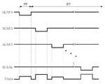
도 6은 도 5에 도시된 구동부들의 출력파형을 보여 주는 파형도.6 is a waveform diagram illustrating output waveforms of the driving units illustrated in FIG. 5.
도 7은 도 5에 도시된 화소의 제1 실시예를 보여 주는 등가 회로도.7 is an equivalent circuit diagram showing a first embodiment of the pixel shown in FIG.
도 8은 도 5에 도시된 화소의 제2 실시예를 보여 주는 등가 회로도.8 is an equivalent circuit diagram showing a second embodiment of the pixel shown in FIG.
도 9는 본 발명의 제2 실시예에 따른 유기발광다이오드 표시소자를 나타내는 블록도.9 is a block diagram illustrating an organic light emitting diode display device according to a second exemplary embodiment of the present invention.
도 10은 도 9에 도시된 구동부들의 출력파형을 보여 주는 파형도.FIG. 10 is a waveform diagram illustrating output waveforms of the driving units illustrated in FIG. 9. FIG.
도 11은 도 9에 도시된 화소의 제1 실시예를 보여 주는 등가 회로도.FIG. 11 is an equivalent circuit diagram showing a first embodiment of the pixel shown in FIG.
도 12는 도 9에 도시된 화소의 제2 실시예를 보여 주는 등가 회로도.12 is an equivalent circuit diagram showing a second embodiment of the pixel shown in FIG.
< 도면의 주요 부분에 대한 부호의 설명 >Description of the Related Art
50, 90 : 표시패널51, 91 : 타이밍 콘트롤러50, 90:
52, 92 : 데이터 구동부53, 93 : 게이트 구동부52, 92:
54, 94 : 화소M1 내지 M6 : 박막트랜지스터54, 94: pixels M1 to M6: thin film transistors
Cs : 스토리지 커패시터PP : 프로그래밍기간Cs: Storage Capacitor PP: Programming Period
EP : 빛방출기간EP: Light emission period
본 발명은 유기발광다이오드 표시소자에 관한 것으로 특히, 구동전압 공급배선으로 인한 전압강하와 박막트랜지스터의 문턱치 전압 변동으로 인한 악영향을 최소화하여 표시 휘도를 균일하게 하도록 한 유기발광다이오드 표시소자에 관한 것이다.BACKGROUND OF THE
최근, 음극선관(Cathode Ray Tube)의 단점인 무게와 부피를 줄일 수 있는 각종 평판 표시장치들이 개발되고 있다. 이러한 평판 표시장치는 액정 표시장 치(Liquid Crystal Display : 이하 "LCD"라 한다), 전계 방출 표시장치(Field Emission Display : FED), 플라즈마 디스플레이 패널(Plasma Display Panel : 이하 "PDP"라 한다) 및 전계발광소자(Electroluminescence Device) 등이 있다.2. Description of the Related Art Recently, various flat panel display devices capable of reducing weight and volume, which are disadvantages of cathode ray tubes (CRTs), have been developed. Such flat panel displays include liquid crystal displays (hereinafter referred to as "LCDs"), field emission displays (FEDs), plasma display panels (hereinafter referred to as "PDPs"), and Electroluminescence devices, and the like.
이들 중에 PDP는 구조와 제조공정이 단순하기 때문에 경박단소하면서도 대화면화에 가장 유리한 표시장치로 주목받고 있지만 발광효율과 휘도가 낮고 소비전력이 큰 단점이 있다. 스위칭 소자로 박막 트랜지스터(Thin Film Transistor : 이하 "TFT"라 한다)가 적용된 액티브 매트릭스 LCD는 반도체공정을 이용하기 때문에 대화면화에 어려움이 있지만 노트북 컴퓨터의 표시소자로 주로 이용되면서 수요가 늘고 있다. 이에 비하여, 전계발광소자는 발광층의 재료에 따라 무기 전계발광소자와 유기발광다이오드소자로 대별되며 스스로 발광하는 자발광소자로서 응답속도가 빠르고 발광효율, 휘도 및 시야각이 큰 장점이 있다.Among them, PDP is attracting attention as the most favorable display device for light and small size and large screen because of its simple structure and manufacturing process, but it has the disadvantages of low luminous efficiency, low luminance and high power consumption. Active matrix LCDs with thin film transistors (hereinafter referred to as "TFTs") as switching devices are difficult to screen due to the use of semiconductor processes, but demand is increasing as they are mainly used as display devices in notebook computers. In contrast, the electroluminescent device is classified into an inorganic electroluminescent device and an organic light emitting diode device according to the material of the light emitting layer. The electroluminescent device is a self-light emitting device that emits light.
유기발광다이오드소자는 도 1과 같이 유리기판 상에 투명도전성물질로 이루어진 애노드전극을 형성하고, 유기 화합물층 및 도전성 금속으로 된 캐소드전극이 적층된다.In the organic light emitting diode device, an anode electrode made of a transparent conductive material is formed on a glass substrate as shown in FIG.
유기 화합물층은 정공주입층(Hole Injection layer), 정공수송층(Hole transport layer, HTL), 발광층(Emission layer, EML), 전자수송층(Electron transport layer, ETL) 및 전자주입층(Electron Injection layer)을 포함한다.The organic compound layer includes a hole injection layer, a hole transport layer (HTL), an emission layer (EML), an electron transport layer (ETL), and an electron injection layer. do.
애노드전극과 캐소드전극에 구동전압이 인가되면 정공주입층 내의 정공과 전자주입층 내의 전자는 각각 발광층 쪽으로 진행하여 발광층을 여기시키고, 그 결과 발광층이 가시광을 발산하게 한다. 이렇게 발광층으로부터 발생되는 가시광으로 화상 또는 영상을 표시하게 된다.When a driving voltage is applied to the anode electrode and the cathode electrode, holes in the hole injection layer and electrons in the electron injection layer proceed toward the light emitting layer to excite the light emitting layer, thereby causing the light emitting layer to emit visible light. Thus, an image or an image is displayed by the visible light generated from the light emitting layer.
이와 같은 유기발광다이오드소자는 패씨브 매트릭스(passive matrix) 방식 또는, 스위칭소자로써 TFT를 이용하는 액티브 매트릭스(active matrix) 방식의 표시소자로 응용되고 있다. 패씨브 매트릭스 방식은 애노드전극과 캐소드전극을 직교하여 그 전극들에 인가되는 전류에 따라 발광셀을 선택하는데 비하여, 액티브 매트릭스 방식은 능동소자인 TFT를 선택적으로 턴-온시켜 발광셀을 선택하고 스토리지 커패시터(Storgage Capacitor)에 유지되는 전압으로 발광셀의 발광을 유지한다.Such an organic light emitting diode device has been applied as a passive matrix display device or an active matrix display device using a TFT as a switching device. In the passive matrix method, the anode and cathode electrodes are orthogonal to select the light emitting cells according to the currents applied to the electrodes, whereas the active matrix method selectively turns on the active TFTs to select and store the light emitting cells. The light emission of the light emitting cell is maintained at a voltage maintained in a capacitor.
도 2는 액티브 매트릭스 방식의 유기발광다이오드 표시소자에 있어서 하나의 화소를 등가적으로 나타내는 회로도이다.2 is an equivalent circuit diagram of one pixel in an organic light emitting diode display device of an active matrix type.
도 2를 참조하면, 액티브 매트릭스 방식의 유기발광다이오드 표시소자는 유기발광다이오드소자(OLED), 서로 교차하는 데이터라인(DL) 및 게이트라인(GL), 스위치 TFT(T2), 구동 TFT(T1), 및 스토리지 커패시터(Cst)를 구비한다. 구동 TFT(T1)와 스위치 TFT(T2)는 P-타입 MOS-FET로 구현된다.Referring to FIG. 2, the organic light emitting diode display device of the active matrix method includes the organic light emitting diode OLED, the data lines DL and gate lines GL, the switch TFT T2, and the driving TFT T1 that cross each other. , And a storage capacitor Cst. The driving TFT T1 and the switch TFT T2 are implemented with a P-type MOS-FET.
스위치 TFT(T2)는 게이트라인(GL)으로부터의 게이트로우전압(또는 스캔전압)에 응답하여 턴-온됨으로써 자신의 소스전극와 드레인전극 사이의 전류패스를 도통시키고, 게이트라인(GL) 상의 전압이 자신의 문턱전압(Threshold Voltage : Vth) 이하인 게이트하이전압일 때 오프 상태를 유지하게 된다. 이 스위치 TFT(T2)의 온타임기간 동안 데이터라인(DL)으로부터의 데이터전압은 스위치 TFT(T2)의 소스전극와 드레인전극를 경유하여 구동 TFT(T1)의 게이트전극와 스토리지 커패시터(Cst)에 인가된다. 이와 반대로, 스위치 TFT(T2)의 오프타임 기간 동안 스위치 TFT(T2)의 소스전극와 드레인전극 사이의 전류패스가 개방되어 데이터전압(VDL)이 구동 TFT(T1)와 스토리지 커패시터(Cst)에 인가되지 않는다.The switch TFT T2 is turned on in response to the gate low voltage (or scan voltage) from the gate line GL to conduct a current path between its source electrode and the drain electrode, and the voltage on the gate line GL When the gate high voltage is less than its threshold voltage (Vth) is maintained off. During the on-time period of the switch TFT T2, the data voltage from the data line DL is applied to the gate electrode and the storage capacitor Cst of the driving TFT T1 via the source electrode and the drain electrode of the switch TFT T2. On the contrary, the current path between the source electrode and the drain electrode of the switch TFT T2 is opened during the off time period of the switch TFT T2 so that the data voltage VDL is not applied to the driving TFT T1 and the storage capacitor Cst. Do not.
구동 TFT(T1)의 소스 전극는 구동전압라인(VL) 및 스토리지 커패시터(Cst)의 일측 전극에 접속되고, 드레인 전극는 유기발광다이오드소자(OLED)의 애노드전극에 접속된다. 그리고 구동 TFT(T1)의 게이트전극는 스위치 TFT(T2)의 드레인전극에 접속된다. 이 구동 TFT(T1)는 게이트전극에 공급되는 게이트전압 즉, 데이터전압에 따라 소스전극와 드레인전극간의 전류양을 조절하여 데이터전압에 대응하는 밝기로 유기발광다이오드소자(OLED)를 발광시킨다.The source electrode of the driving TFT T1 is connected to one side of the driving voltage line VL and the storage capacitor Cst, and the drain electrode is connected to the anode electrode of the organic light emitting diode device OLED. The gate electrode of the driving TFT T1 is connected to the drain electrode of the switch TFT T2. The driving TFT T1 adjusts the amount of current between the source electrode and the drain electrode according to the gate voltage supplied to the gate electrode, that is, the data voltage, and emits the organic light emitting diode OLED with brightness corresponding to the data voltage.
스토리지 커패시터(Cst)는 데이터전압과 고전위 구동전압(VDD) 사이의 차전압을 저장하여 구동 TFT(T1)의 게이트전극에 인가되는 전압을 한 프레임기간동안 일정하게 유지시킨다.The storage capacitor Cst stores the difference voltage between the data voltage and the high potential driving voltage VDD to maintain a constant voltage applied to the gate electrode of the driving TFT T1 for one frame period.
유기발광다이오드소자(OLED)는 도 1과 같은 구조로 구현되고 구동 TFT(T1)의 드레인전극에 접속된 캐소드전극와 기저전압원(GND)이 공급되는 캐소드전극를 포함한다. 이 유기발광다이오드소자(OLED)는 구동 TFT(T1)의 게이트전압에 따라 결정되는 구동 TFT(T1)의 소스-드레인간 전류에 의해 발광한다.The organic light emitting diode OLED has a structure as shown in FIG. 1 and includes a cathode electrode connected to the drain electrode of the driving TFT T1 and a cathode electrode supplied with a ground voltage source GND. The organic light emitting diode OLED emits light by the source-drain current of the driving TFT T1 determined in accordance with the gate voltage of the driving TFT T1.
도 2와 같은 유기발광다이오드 표시소자는 구동 TFT(T1)의 특성에 따라 유기발광다이오드소자(OLED)에 흐르는 전류가 결정된다. 따라서, 구동 TFT(T1)의 특성이 각 화소들에서 균일하게 되어야만 균일한 휘도 특성으로 화상을 표시할 수 있지만, 실제로 제작되는 패널에서 구동 TFT(T1)의 특성 예컨대, 문턱전압 특성이 화면 위치에 따라 다르게 되고 구동전압라인(VL)으로 인한 고전위 구동전압(VDD)의 전압 강하로 인하여 동일 데이터에서 화면 위치에 따라 휘도가 다르게 된다.In the organic light emitting diode display device of FIG. 2, a current flowing through the organic light emitting diode device OLED is determined according to the characteristics of the driving TFT T1. Therefore, although the characteristics of the driving TFT T1 must be uniform in each pixel to display an image with uniform brightness characteristics, the characteristics of the driving TFT T1, for example, the threshold voltage characteristic, are not displayed at the screen position in the panel actually manufactured. The luminance varies depending on the screen position in the same data due to the voltage drop of the high potential driving voltage VDD due to the driving voltage line VL.
도 3은 액티브 매트릭스 방식의 유기발광다이오드 표시소자에서 TFT 특히, 구동 TFT(T1)의 문턱전압 편차와 구동전압라인(VL)으로 인한 전압 강하에 의해 동일 계조의 데이터에서 나타나는 실제 화면의 세로 줄무늬 현상을 보여 준다.FIG. 3 is a vertical fringe of an actual screen which appears in data of the same gray scale due to a voltage drop caused by a threshold voltage deviation of a TFT, in particular, a driving TFT T1 and a driving voltage line VL in an active matrix organic light emitting diode display device. Shows.
예를 들면, 도 4와 같은 레이저 결정화 공정에서 유기발광다이오드 표시소자의 TFT 기판에 형성된 비정질 실리콘(a-Si)이 폴리 실리콘(p-Si)으로 결정화될 때 레이저의 파워가 시간에 따라 불안정하게 되는 것과 또한, 기판 면에 대하여 일정 부분씩 스캔하면서 레이저를 조사할 때 시간차를 두고 레이저가 조사된 부분들 사이의 경계에서 나타나는 실리콘 박막의 막질이 불균일해지는 것에 의해 TFT 기판의 반도체 특성이 불균일해진다. 이렇게 TFT 기판의 반도체 특성이 위치에 따라 편차가 나타날 때 도 3의 줄무늬 현상과 같이 동일 계조의 데이터에서도 휘도가 불균일하게 나타난다.For example, when the amorphous silicon (a-Si) formed on the TFT substrate of the organic light emitting diode display device is crystallized to polysilicon (p-Si) in the laser crystallization process as shown in FIG. 4, the power of the laser becomes unstable over time. In addition, the semiconductor characteristics of the TFT substrate become uneven due to the uneven film quality of the silicon thin film appearing at the boundary between the portions irradiated with the laser at a time difference when the laser is irradiated while scanning a portion of the substrate surface. Thus, when the semiconductor characteristics of the TFT substrate vary depending on the position, the luminance appears uneven even in the data of the same gray scale as in the stripe phenomenon of FIG.
따라서, 본 발명의 목적은 구동전압 공급배선으로 인한 전압강하와 TFT의 문턱치 전압 변동으로 인한 악영향을 최소화하여 표시 휘도를 균일하게 하도록 한 유기발광다이오드 표시소자를 제공하는데 있다.Accordingly, an object of the present invention is to provide an organic light emitting diode display device which minimizes adverse effects caused by voltage drops due to driving voltage supply wiring and threshold voltage variations of TFTs, thereby making the display brightness uniform.
상기 목적을 달성하기 위하여, 본 발명의 제1 실시예에 따른 유기발광다이오 드 표시소자는 구동전압을 발생하는 구동전압원; 기준전압을 발생하는 기준전압원; 기준전류를 발생하는 기준전류원; 제1 노드와 제2 노드 사이에 접속된 스토리지 커패시터; 제3 노드와 기저전압원 사이에 접속된 유기발광다이오드소자; 제1 스캔신호가 공급되는 제1 스캔라인; 상기 제1 스캔신호에 대하여 역위상으로 발생되는 제2 스캔신호가 공급되는 제2 스캔라인; 상기 스캔라인들과 교차하고 데이터전압이 공급되는 데이터라인; 제1 기간 동안 오프 상태를 유지한 후, 제2 기간 동안 상기 제1 스캔신호에 응답하여 상기 제1 노드에 상기 기준전압을 공급하는 제1 스위치소자; 상기 제1 기간 동안 상기 제2 스캔신호에 응답하여 상기 제1 노드에 상기 데이터전압을 공급한 후, 상기 제2 기간 동안 오프 상태를 유지하는 제2 스위치소자; 상기 제2 노드의 전압에 따라 상기 유기발광다이오드소자로 공급되는 전류를 조절하는 제3 스위치소자; 상기 제1 기간 동안 상기 제2 스캔신호에 응답하여 상기 기준전류를 상기 제2 노드에 공급한 후, 상기 제2 기간 동안 오프 상태를 유지하는 제4 스위치소자; 상기 제1 기간 동안 상기 제2 스캔신호에 응답하여 상기 제2 노드와 상기 제3 노드 사이의 전류패스를 형성한 후, 상기 제2 기간 동안 오프 상태를 유지하는 제5 스위치소자; 및 상기 제1 기간 동안 상기 제3 노드를 경유하여 상기 유기발광다이오드소자로 흐르는 전류를 차단한 후, 상기 제2 기간 동안 상기 제1 스캔신호와 상기 제2 노드의 전압 중 어느 하나에 응답하여 상기 제3 노드와 상기 유기발광다이오드소자 사이의 전류패스를 형성하는 제6 스위치소자를 구비한다.In order to achieve the above object, the organic light emitting diode display device according to the first embodiment of the present invention comprises a driving voltage source for generating a driving voltage; A reference voltage source for generating a reference voltage; A reference current source for generating a reference current; A storage capacitor connected between the first node and the second node; An organic light emitting diode element connected between the third node and the base voltage source; A first scan line to which a first scan signal is supplied; A second scan line supplied with a second scan signal generated out of phase with respect to the first scan signal; A data line crossing the scan lines and supplied with a data voltage; A first switch element which maintains an off state for a first period and supplies the reference voltage to the first node in response to the first scan signal during a second period; A second switch element configured to maintain the off state during the second period after supplying the data voltage to the first node in response to the second scan signal during the first period; A third switch element configured to adjust a current supplied to the organic light emitting diode element according to the voltage of the second node; A fourth switch element configured to maintain the off state during the second period after supplying the reference current to the second node in response to the second scan signal during the first period; A fifth switch element configured to maintain an off state during the second period after forming a current path between the second node and the third node in response to the second scan signal during the first period; And blocking current flowing through the organic light emitting diode device through the third node during the first period, and then responding to any one of the first scan signal and the voltage of the second node during the second period. And a sixth switch element forming a current path between the third node and the organic light emitting diode element.
본 발명의 제2 실시예에 따른 유기발광다이오드 표시소자는 구동전압을 발생하는 구동전압원; 기준전압을 발생하는 기준전압원; 기준전류를 발생하는 기준전류 원; 제1 노드와 제2 노드 사이에 접속된 스토리지 커패시터; 제3 노드와 기저전압원 사이에 접속된 유기발광다이오드소자; 스캔신호가 공급되는 스캔라인; 상기 스캔라인과 교차하고 데이터전압이 공급되는 데이터라인; 제1 기간 동안 상기 스캔신호의 제1 전압에 응답하여 오프 상태를 유지한 후제2 기간 동안 상기 스캔신호의 제2 전압에 응답하여 상기 제1 노드에 상기 기준전압을 공급하는 제1 스위치소자; 상기 제1 기간 동안 상기 스캔신호의 제1 전압에 응답하여 상기 제1 노드에 상기 데이터전압을 공급한 후, 상기 제2 기간 동안 오프 상태를 유지하는 제2 스위치소자; 상기 제2 노드의 전압에 따라 상기 유기발광다이오드소자로 공급되는 전류를 조절하는 제3 스위치소자; 상기 제1 기간 동안 상기 스캔신호의 제1 전압에 응답하여 상기 기준전류를 상기 제2 노드에 공급한 후, 상기 제2 기간 동안 오프 상태를 유지하는 제4 스위치소자; 상기 제1 기간 동안 상기 스캔신호의 제1 전압에 응답하여 상기 제2 노드와 상기 제3 노드 사이의 전류패스를 형성한 후, 상기 제2 기간 동안 오프 상태를 유지하는 제5 스위치소자; 및 상기 제1 기간 동안 상기 제3 노드를 경유하여 상기 유기발광다이오드소자로 흐르는 전류를 차단한 후, 상기 제2 기간 동안 상기 제2 노드의 전압과 상기 스캔신호의 제2 전압 중 어느 하나에 응답하여 상기 제3 노드와 상기 유기발광다이오드소자 사이의 전류패스를 형성하는 제6 스위치소자를 구비한다.An organic light emitting diode display device according to a second embodiment of the present invention includes a driving voltage source for generating a driving voltage; A reference voltage source for generating a reference voltage; A reference current source for generating a reference current; A storage capacitor connected between the first node and the second node; An organic light emitting diode element connected between the third node and the base voltage source; A scan line to which a scan signal is supplied; A data line crossing the scan line and supplied with a data voltage; A first switch element configured to maintain an off state in response to a first voltage of the scan signal during a first period, and then supply the reference voltage to the first node in response to a second voltage of the scan signal during a second period; A second switch element which supplies the data voltage to the first node in response to the first voltage of the scan signal during the first period, and then maintains an off state for the second period; A third switch element configured to adjust a current supplied to the organic light emitting diode element according to the voltage of the second node; A fourth switch element which supplies the reference current to the second node in response to the first voltage of the scan signal during the first period, and then maintains an off state for the second period; A fifth switch element which maintains an off state during the second period after forming a current path between the second node and the third node in response to the first voltage of the scan signal during the first period; And after blocking a current flowing to the organic light emitting diode device through the third node during the first period, responding to one of a voltage of the second node and a second voltage of the scan signal during the second period. And a sixth switch element forming a current path between the third node and the organic light emitting diode element.
이하, 도 5 내지 도 12를 참조하여 본 발명의 바람직한 실시예들에 대하여 설명하기로 한다.Hereinafter, exemplary embodiments of the present invention will be described with reference to FIGS. 5 to 12.
도 5 내지 도 8을 참조하면, 본 발명의 제1 실시예에 따른 유기발광다이오드 표시소자는 m×n 개의 화소들(54)이 형성되는 표시패널(50)과, 데이터라인들(DL1 내지 DLm)에 데이터전압을 공급하기 위한 데이터 구동부(52)와, m 개의 스캔전극쌍(E1 내지 En, S1 내지 Sn)에 상호 역위상의 스캔펄스쌍을 순차적으로 공급하기 위한 스캔 구동부(53)와, 상기 구동부들(52, 53)을 제어하기 위한 타이밍 콘트롤러(51)를 구비한다.5 to 8, an organic light emitting diode display according to a first exemplary embodiment of the present invention includes a
표시패널(50)에서, 각각 n 개의 제1 및 제2 스캔라인들(E1 내지 En, S1 내지 Sn)과, m 개의 데이터라인들(DL1 내지 DLm)의 교차로 정의된 화소 영역들에 화소들(54)이 형성된다. 이러한 표시패널(50)에는 정전압의 기준전압(Vref), 정전류의 기준전류(Iref), 및 고전위 구동전압(VDD)을 각각의 화소들(54)에 공급하기 위한 신호배선들이 형성된다.In the
데이터 구동부(52)는 타이밍 콘트롤러(51)로부터의 디지털 비디오 데이터(RGB)를 아날로그 감마보상전압으로 변환한다. 그리고 데이터 구동부(52)는 각 화소(54)의 유기발광다이오드소자(OLED)가 발광되기 전에 할당된 프로그래밍기간(PP) 동안, 타이밍 콘트롤러(51)로부터의 제어신호(DDC)에 응답하여 아날로그 감마보상전압을 데이터전압(Vdata)으로써 데이터라인들(DL1 내지 DLm)에 공급한다.The
스캔 구동부(53)는 타이밍 콘트롤러(51)로부터의 제어신호(SDC)에 응답하여 도 6과 같이 하이전압의 제1 스캔펄스(EM1 내지 EMn)를 제1 스캔라인들(E1 내지 En)에 순차적으로 공급함과 동시에, 로우전압의 제2 스캔펄스(SCAN1 내지 SCANn)를 제1 스캔펄스(EM1 내지 EMn)에 대하여 역위상으로 발생하고 그 제2 스캔펄스(SCAN1 내지 SCANn)를 제1 스캔펄스(EM1 내지 EMn)와 동기되도록 제2 스캔라인들(S1 내지 Sn)에 순차적으로 공급한다.In response to the control signal SDC from the
타이밍 콘트롤러(51)는 디지털 비디오 데이터(RGB)를 데이터 구동부(52)에 공급하고 수직/수평 동기신호와 클럭신호 등을 이용하여 스캔 구동부(53)와 데이터 구동부(52)의 동작 타이밍을 제어하기 위한 제어신호(DDC, SDC)를 발생한다.The
한편, 표시패널(50)에는 기준전압(Vref)과 고전위 구동전압(VDD)을 공급하기 위한 정전압원과, 기준전류(Iref)을 공급하기 위한 정전류원이 접속된다.On the other hand, the
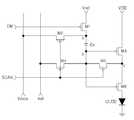
화소들(54) 각각은 도 7 및 도 8과 같이 유기발광다이오드소자(OLED), 6 개의 TFT, 및 1 개의 스토리지 커패시터를 포함한다.Each of the
도 7은 본 발명에 따른 유기발광다이오드 표시소자에서 화소들(54)의 제1 실시예를 나타낸다.7 shows a first embodiment of the
도 7을 참조하면, 제1 TFT(M1)는 제1 스캔라인(E1 내지 En)으로부터 공급되는 제2 스캔펄스(EM1 내지 EMn)에 의해 프로그래밍기간(PP) 동안 오프 상태를 유지하는 반면, 빛방출기간(EP) 동안 기준전압원(Vref)과 a 노드 사이의 전류패스를 형성한다. 이 제1 TFT(M1)의 게이트전극은 제1 스캔라인(E1 내지 En)에 접속되고, 소스전극은 기준전압원(Vref)에 접속된다. 그리고 제1 TFT(M1)의 드레인전극은 a 노드에 접속된다.Referring to FIG. 7, the first TFT M1 is maintained in the off state for the programming period PP by the second scan pulses EM1 to EMn supplied from the first scan lines E1 to En. During the emission period EP, a current path is formed between the reference voltage source Vref and node a. The gate electrode of this first TFT M1 is connected to the first scan lines E1 to En, and the source electrode is connected to the reference voltage source Vref. The drain electrode of the first TFT M1 is connected to a node.
제2 TFT(M2)는 제2 스캔라인(S1 내지 Sn)으로부터 공급되는 제2 스캔펄스(SCAN1 내지 SCANn)에 의해 턴-온되어 프로그래밍기간(PP) 동안, 데이터라인(DL1 내지 DLm)과 a 노드 사이의 전류패스를 연결하여 스토리지 커패시터(Cs)에 데이터전압(Vdata)을 충전시키는 반면, 빛방출기간(EP) 동안 데이터라인(DL1 내지 DLm)과 a 노드 사이의 전류패스를 차단한다. 이 제2 TFT(M2)의 게이트전극은 제2 스캔라인(SCAN1 내지 SCANn)에 접속되고, 소스전극은 데이터라인(DL1 내지 DLm)에 접속된다. 그리고 제2 TFT(M2)의 드레인전극은 a 노드에 접속된다.The second TFT M2 is turned on by the second scan pulses SCAN1 to SCANn supplied from the second scan lines S1 to Sn, and during the programming period PP, the data lines DL1 to DLm and a The current path between the nodes is connected to charge the data voltage Vdata to the storage capacitor Cs, while the current path between the data lines DL1 to DLm and a node is blocked during the light emission period EP. The gate electrode of this second TFT M2 is connected to the second scan lines SCAN1 to SCANn, and the source electrode is connected to the data lines DL1 to DLm. The drain electrode of the second TFT M2 is connected to a node.
제3 TFT(M3)는 구동 TFT로써 프로그래밍기간(PP)과 빛방출기간(EP) 동안, 게이트전압인 b 노드 전압에 응답하여 턴-온되어 고전위 구동전압원(VDD)과 c 노드 사이의 전류패스를 연결한다. 이 제3 TFT(M3)의 게이트전극은 b 노드에 접속되고, 소스전극은 고전위 구동전압원(VDD)에 접속된다. 그리고 제3 TFT(M3)의 드레인전극은 c 노드에 접속된다.The third TFT M3 is a driving TFT and is turned on in response to the b-node voltage, which is a gate voltage, during the programming period PP and the light emission period EP, so that the current between the high potential driving voltage source VDD and the c-node. Connect the paths. The gate electrode of this third TFT M3 is connected to the node b, and the source electrode is connected to the high potential driving voltage source VDD. The drain electrode of the third TFT M3 is connected to the c node.
제4 TFT(M4)는 제2 스캔라인(S1 내지 Sn)으로부터 공급되는 제2 스캔펄스(SCAN1 내지 SCANn)에 의해 턴-온되어 프로그래밍기간(PP) 동안, b 노드와 정전류원(Iref) 사이의 전류패스를 연결하는 반면, 빛방출기간(EP) 동안 b 노드와 정전류원(Iref) 사이의 전류패스를 차단한다. 이 제4 TFT(M4)의 게이트전극은 제2 스캔라인(S1 내지 Sn)에 접속되고, 소스전극은 b 노드에 접속된다. 그리고 제4 TFT(M4)의 드레인전극은 정전류원(Iref)에 접속된다.The fourth TFT M4 is turned on by the second scan pulses SCAN1 to SCANn supplied from the second scan lines S1 to Sn, and is connected between the node b and the constant current source Iref during the programming period PP. While connecting the current path, the current path between the node b and the constant current source (Iref) is blocked during the light emission period (EP). The gate electrode of this fourth TFT M4 is connected to the second scan lines S1 to Sn, and the source electrode is connected to the b node. The drain electrode of the fourth TFT M4 is connected to the constant current source Iref.
제5 TFT(M5)는 제4 TFT(M4)와 유사하게, 제2 스캔라인(S1 내지 Sn)으로부터 공급되는 제2 스캔펄스(SCAN1 내지 SCANn)에 의해 턴-온되어 프로그래밍기간(PP) 동안, b 노드와 c 노드 사이의 전류패스를 연결하는 반면, 빛방출기간(EP) 동안 b 노드와 c 노드 사이의 전류패스를 차단한다. 이 제5 TFT(M5)의 게이트전극은 제2 스캔라인(S1 내지 Sn)에 접속되고, 소스전극은 c 노드에 접속된다. 그리고 제5 TFT(M5)의 드레인전극은 b 노드에 접속된다.The fifth TFT M5 is turned on by the second scan pulses SCAN1 to SCANn supplied from the second scan lines S1 to Sn, similarly to the fourth TFT M4, for the programming period PP. The current path between node b and node c is connected, while the current path between node b and node c is blocked during the light emission period (EP). The gate electrode of this fifth TFT M5 is connected to the second scan lines S1 to Sn, and the source electrode is connected to the c node. The drain electrode of the fifth TFT M5 is connected to the b node.
제6 TFT(M6)는 제1 스캔라인(E1 내지 En)으로부터 공급되는 제2 스캔펄스(EM1 내지 EMn)에 의해 프로그래밍기간(PP) 동안 오프 상태를 유지하는 반면, 빛방출기간(EP) 동안 c 노드와 유기발광다이오드소자(OLED) 사이의 전류패스를 형성한다. 이 제6 TFT(M6)의 게이트전극은 제1 스캔라인(E1 내지 En)에 접속되고, 소스전극은 c 노드에 접속된다. 그리고 제6 TFT(M6)의 드레인전극은 유기발광다이오드소자(OLED)의 애노드전극에 접속된다.The sixth TFT M6 is kept off for the programming period PP by the second scan pulses EM1 to EMn supplied from the first scan lines E1 to En, while the light emission period EP is maintained. A current path is formed between the c-node and the organic light emitting diode device (OLED). The gate electrode of this sixth TFT M6 is connected to the first scan lines E1 to En, and the source electrode is connected to the c node. The drain electrode of the sixth TFT M6 is connected to the anode electrode of the organic light emitting diode element OLED.
스토리지 커패시터(Cs)는 프로그래밍기간 동안(PP) 문턱전압 성분과 구동전압(VDD) 성분을 충전한 후, 빛방출기간(EP) 동안 충전된 전압을 유지한다.The storage capacitor Cs charges the threshold voltage component and the driving voltage VDD component during the programming period PP and maintains the charged voltage during the light emission period EP.
유기발광다이오드소자(OLED)는 도 1과 같은 구조를 가지며, 빛방출기간(EP) 동안 도 7의 점선과 같이 제3 TFT(M3)와 제6 TFT(M6)를 경유하여 흐르는 전류(IOLED)에 의해 발광한다.The organic light emitting diode OLED has the structure as shown in FIG. 1 and the current IOLED flowing through the third TFT M3 and the sixth TFT M6 during the light emission period EP as shown by the dotted line of FIG. 7. Emits light by
제1 TFT(M1)는 프로그래밍기간(PP) 동안 스토리지 커패시터(Cs)의 일측 전극에 기준 전압(Vdata)을 충전시키고, 기준전압(Vref)을 이용하여 스토리지 커패시터(Cs)의 타측 전극과 제3 TFT(M3)의 게이트전극에 제3 TFT(M3)의 문턱전압과 고전위 구동전압(VDD) 정보를 갖고 있는 구동전압을 충전시킨다.The first TFT M1 charges the reference voltage Vdata to one electrode of the storage capacitor Cs during the programming period PP, and uses the reference voltage Vref and the third electrode and the third electrode of the storage capacitor Cs. The gate electrode of the TFT M3 is charged with a driving voltage having the threshold voltage and the high potential driving voltage VDD information of the third TFT M3.
제2, 제4, 및 제5 TFT(M2, M4, M5)는 프로그래밍기간(PP) 동안 스토리지 커패시터(Cs)의 일측 전극에 데이터 전압(Vdata)을 충전시키고, 기준전류(Iref)를 이용하여 스토리지 커패시터(Cs)의 타측 전극에 제3 TFT(M3)의 문턱전압을 충전시켜 데이터 전압(Vdata)의 스캐닝과 문턱전압의 샘플링 동작을 수행한다.The second, fourth, and fifth TFTs M2, M4, and M5 charge the data voltage Vdata to one electrode of the storage capacitor Cs during the programming period PP, and use the reference current Iref. The threshold voltage of the third TFT M3 is charged to the other electrode of the storage capacitor Cs to perform scanning of the data voltage Vdata and sampling of the threshold voltage.
이러한 화소들(54)의 동작을 단계적으로 설명하면 다음과 같다.The operation of these
프로그래밍기간(PP) 동안, 제1 스캔펄스(EM1 내지 EMn)는 하이전압을 유지하여 제1 및 제6 TFT(M1, M6)를 턴-오프시키고, 제2 스캔펄스(SCAN1 내지 SCANn)는 로우전압을 유지하여 제2, 제4 및 제5 TFT(M2, M4, M5)를 턴-온시킨다. 따라서, 데이터라인(DL1 내지 DLm)으로부터의 데이터전압(Vdata)은 제2 TFT(M2)를 경유하여 a 노드에 접속된 스토리지 커패시터(Cs)의 일측 전극에 충전된다. b 노드에 접속된 스토리지 커패시터(Cs)의 타측 전극에는 제3 TFT(M3)의 소스전압보다 문턱전압 이상으로 낮은 게이트전압으로 충전된다. 이와 동시에 제3 TFT(M3)는 턴-온된 제5 TFT(M3)를 통해 다이오드소자로 결선된다. 따라서, 프로그래밍기간(PP) 동안 다이오드로 동작하는 제3 TFT(M3)에 의해 기준전류(Iref)가 도 7의 실선과 같이 고전위 구동전압원(VDD) -> 제3 TFT(M3) -> 제5 TFT(M5) -> 제4 TFT(M4) -> 정전류원(Iref)으로 전류가 흐르게 된다. 이 프로그래밍 동안, 제1 TFT(M1)의 드레인전극과 스토리지 커패시터(Cs) 사이의 a 노드 전압(Va), 스토리지 커패시터(Cs)와 제3 TFT(M3)의 게이트전극 사이의 b 노드 전압(Vb)은 아래의 수학식 1, 2과 같다.During the programming period PP, the first scan pulses EM1 to EMn maintain a high voltage to turn off the first and sixth TFTs M1 and M6, and the second scan pulses SCAN1 to SCANn turn low. The second, fourth and fifth TFTs M2, M4 and M5 are turned on by maintaining the voltage. Therefore, the data voltage Vdata from the data lines DL1 to DLm is charged to one electrode of the storage capacitor Cs connected to the node a via the second TFT M2. The other electrode of the storage capacitor Cs connected to the node b is charged with a gate voltage lower than the threshold voltage of the source voltage of the third TFT M3. At the same time, the third TFT M3 is connected to the diode device through the turned-on fifth TFT M3. Accordingly, the reference current Iref is generated by the third TFT M3 operating as a diode during the programming period PP, as shown in the solid line of FIG. 7, from the high potential driving voltage source VDD to the third TFT M3. 5 TFT (M5)-> fourth TFT (M4)-> current flows to the constant current source (Iref). During this programming, the a node voltage Va between the drain electrode of the first TFT M1 and the storage capacitor Cs, and the b node voltage Vb between the storage capacitor Cs and the gate electrode of the third TFT M3. ) Is the same as


수학식 1에서 'Vdata'는 데이터전압이고, 수학식 2에서 'VT''는 아래의 수학 식 3과 같다.In

수학식 3에서 'Vth'는 제3 TFT(M3)의 문턱전압, k'는 제3 TFT(M3)의 이동도 및 기생용량을 함수로 하는 상수값, 'L'은 제3 TFT(M3)의 채널길이, 'W'는 제3 TFT(M3)의 채널폭을 각각 나타낸다.In Equation 3, 'Vth' is a threshold voltage of the third TFT M3, k 'is a constant value that is a function of the mobility and parasitic capacitance of the third TFT M3, and' L 'is the third TFT M3. 'W' indicates the channel width of the third TFT M3, respectively.
수학식 3에서 기준전류(Iref)는 아래의 수학식 4로 정의된다.In Equation 3, the reference current Iref is defined by Equation 4 below.

여기서, 기준전류(Iref)는 제3 TFT(M3)의 문턱전압(VTH)을 감지하기 위한 전류로써 그 전류값이 높을수록 제3 TFT(M3)의 문턱전압을 감지하기 위한 프로그래밍기간을 줄일 수 있으나 그 만큼 소비전력이 증가될 수 있다. 따라서, 기준전류(Iref)는 패널 특성, 구동시간 및 소비전력을 고려하여 실험적으로 결정된다. 예컨대, 기준전류(Iref)는 패널에 형성된 TFT의 반도체특성, 구동주파수 규격 및 소비전력의 요구사항 등에 따라 달라질 수 있다.Here, the reference current Iref is a current for detecting the threshold voltage VTH of the third TFT M3. The higher the current value, the shorter the programming period for detecting the threshold voltage of the third TFT M3. However, the power consumption may increase accordingly. Therefore, the reference current Iref is determined experimentally in consideration of panel characteristics, driving time and power consumption. For example, the reference current Iref may vary depending on the semiconductor characteristics of the TFT formed in the panel, the driving frequency standard, the power consumption requirements, and the like.
빛방출기간(EP) 동안 제1 스캔펄스(EM1 내지 EMn)는 로우전압으로 반전되어 제1 및 제6 TFT(M1, M6)를 턴-온시키고, 제2 스캔펄스(SCAN1 내지 SCANn)는 하이전 압으로 반전되어 제2, 제4 및 제5 TFT(M2, M4, M5)를 턴-오프시킨다. 따라서, 화소(54)로 공급되는 데이터전압(Vdata)과 기준전류(Iref)는 차단되고, 기준전압(Vref)은 제1 TFT(M1)를 경유하여 a 노드에 접속된 스토리지 커패시터(Cs)의 일측 전극에 충전된다. 이 때, b 노드에 접속된 스토리지 커패시터(Cs)의 타측 전극은 기준전압(Vref)에 의해 부트스트랩(bootstrap)되어 그 충전 전위가 변하게 된다. 따라서, 제3 TFT(M3)는 이렇게 변화된 b 노드의 전압에 따라서 빛을 발광하게 된다. 이 빛방출기간(EP) 동안 발광다이오드소자(OLED)는 도 7의 점선과 같이 고전위 구동전압원(VDD) -> 제3 TFT(M3) -> 제6 TFT(M6) -> 발광다이오드소자(OLED) -> 기저전압원(GND)으로 흐르는 전류(IOLED)에 의해 발광한다. 이 빛방출기간(EP) 동안, a 노드 전압(Va)과 b 노드 전압(Vb)은 아래의 수학식 5, 6과 같고 유기발광다이오드소자(OLED)에 흐르는 전류(IOLED)는 수학식 7과 같다.During the light emission period EP, the first scan pulses EM1 to EMn are inverted to a low voltage to turn on the first and sixth TFTs M1 and M6 and the second scan pulses SCAN1 to SCANn Inverted to the previous voltage to turn off the second, fourth and fifth TFTs M2, M4, M5. Accordingly, the data voltage Vdata and the reference current Iref supplied to the


기준전압(Vref)은 빛방출기간(EP) 동안 스토리지 커패시터(Cs)의 일측 전압을 유지시키는 전압으로써 데이터 전압과 기준전류(Iref)의 값으로부터 결정되는 임의의 정전압으로 결정된다.The reference voltage Vref is a voltage for maintaining one side voltage of the storage capacitor Cs during the light emission period EP, and is determined as an arbitrary constant voltage determined from the data voltage and the value of the reference current Iref.

수학식 7에서 알 수 있는 바, 본 발명에 따른 유기발광다이오드 표시소자에서 빛방출기간(EP) 동안 유기발광다이오드소자(OLED)에 흐르는 전류(IOLED)를 정의하는 수식에는 고전위 구동전압(VDD)와 제3 TFT(M3)의 문턱전압(Vth)의 항이 없다. 즉, 빛방출기간(EP) 동안 유기발광다이오드소자(OLED)에 흐르는 전류(IOLED)는 고전위 구동전압(VDD)과 TFT의 문턱전압(Vth)에 전혀 영향을 받지 않는다.As can be seen from Equation 7, the organic light emitting diode display device according to the present invention defines a current IOLED flowing in the organic light emitting diode device OLED during the light emission period EP. There is no term for the threshold voltage Vth of VDD and the third TFT M3. That is, the current IOLED flowing through the organic light emitting diode OLED during the light emission period EP is not affected at all by the high potential driving voltage VDD and the threshold voltage Vth of the TFT.
도 8은 본 발명에 따른 유기발광다이오드 표시소자에서 화소들(54)의 제2 실시예를 나타낸다.8 shows a second embodiment of the
도 8을 참조하면, 화소들(54) 각각은 제1 내지 제6 TFT(M1 내지 M6), 스토리지 커패시터(Cs), 및 유기발광다이오드소자(OLED)를 구비한다. TFT들(M1 내지 M6)은 P 타입 MOS-FET로 구현된다. 제1 내지 제5 TFT(M1 내지 M5), 스토리지 커패시터(Cs) 및 유기발광다이오드소자(OLED)는 전술한 도 6의 실시예에서 설명된 그 것들과 실질적으로 동일하므로 그에 대한 상세한 설명을 생략하기로 한다.Referring to FIG. 8, each of the
제3 TFT(M3)는 전술한 실시예와 같이 프로그래밍기간(PP) 동안 다이오드로 동작하여 기준전류(Iref)를 흐르게 한다.The third TFT M3 operates as a diode during the programming period PP to flow the reference current Iref as in the above-described embodiment.
제6 TFT(M6)는 프로그래밍기간(PP) 동안 턴-온된 제5 TFT(M5)에 의해 역방향 다이오드로 결선되어 유기발광다이오드소자(OLED)로 공급되는 전류(IOLED)를 차단하는 반면, 빛방출기간(EP) 동안 c 노드와 유기발광다이오드소자(OLED) 사이의 전류패스를 형성하여 유기발광다이오드소자(OLED)에 전류(IOLED)를 공급한다. 이 제6 TFT(M6)의 게이트전극은 전술한 제1 실시예와 달리 b 노드에 접속된다. 그리고 제6 TFT(M6)의 소스전극은 c 노드에 접속되며, 드레인전극은 유기발광다이오드소자(OLED)의 애노드전극에 접속된다.The sixth TFT M6 is connected to the reverse diode by the fifth TFT M5 turned on during the programming period PP to block the current IOLED supplied to the organic light emitting diode device OLED, During the emission period EP, a current path is formed between the c-node and the organic light emitting diodeOLED to supply the current IOLED to the organic light emitting diodeOLED . The gate electrode of this sixth TFT (M6) is connected to the node b unlike the first embodiment described above. The source electrode of the sixth TFT M6 is connected to the node c, and the drain electrode is connected to the anode electrode of the organic light emitting diode device OLED.
이러한 도 8의 화소(54)는 전술한 도 6의 실시예와 실질적으로 동일하게 동작한다.The
프로그래밍기간(PP) 동안, 제1 스캔펄스(EM1 내지 EMn)에 의해 제1 TFT(M1)는 턴오프되는 반면에, 제2 스캔펄스(SCAN1 내지 SCANn)에 의해 제2, 제4 및 제5 TFT(M2, M4, M5)는 턴-온된다. 이와 동시에, 제3 TFT(M3)는 턴-온된 제5 TFT(M5)에 의해 순방향 다이오드로 동작하여 기준전류(Iref)를 흐르게 하고 제6 TFT(M1, M6)는 역방향 다이오드로 동작하여 유기발광다이오드소자(OLED)에 공급되는 전류를 차단한다. 이 프로그래밍기간(PP) 동안 a 노드에는 데이터전압(Vdata)이 충전되고 b 노드에 제3 TFT(M3)의 문턱전압이 샘플링된다. 이어서, 빛방출기간(EP) 동안, 제1 스캔펄스(EM1 내지 EMn)의 전압이 반전되어 제2, 제4 및 제5 TFT(M2, M4, M5)는 턴-오프되고, 제1 TFT(M1)는 턴-온된다. 그리고 빛방출기간(EP) 동안 제3 및 제6 TFT(M3, M6)는 고전위 구동전압(VDD)과 문턱전압(Vth)에 영향을 받지 않는 전류(IOLED)를 유기발광다이오드소자(OLED)에 공급한다.During the programming period PP, the first TFT M1 is turned off by the first scan pulses EM1 through EMn, while the second, fourth and fifth are driven by the second scan pulses SCAN1 through SCANn. TFTs M2, M4, and M5 are turned on. At the same time, the third TFT M3 operates as a forward diode by the turned-on fifth TFT M5 to flow the reference current Iref, and the sixth TFT M1 and M6 act as a reverse diode to emit organic light. It cuts off the current supplied to the diode. During this programming period PP, the data voltage Vdata is charged to node a and the threshold voltage of the third TFT M3 is sampled to node b. Subsequently, during the light emission period EP, the voltages of the first scan pulses EM1 to EMn are inverted so that the second, fourth and fifth TFTs M2, M4, and M5 are turned off and the first TFT ( M1) is turned on. During the light emission period EP, the third and sixth TFTs M3 and M6 receive a current IOLED that is not affected by the high potential driving voltage VDD and the threshold voltage Vth, and the organic light emitting diode device OLED Supplies).
도 9 내지 도 12는 N 타입 MOS-FET와 P 타입 MOS-FET를 동일 기판 상에 함께 형성하는 CMOS(Complementary Metal Oxide Semiconductor) 공정에서 적용 가능한 유기발광다이오드 표시소자의 실시예를 나타낸다.9 through 12 illustrate embodiments of an organic light emitting diode display device applicable to a CMOS (Complementary Metal Oxide Semiconductor) process in which an N-type MOS-FET and a P-type MOS-FET are formed together on the same substrate.
도 9 내지 도 12를 참조하면, 본 발명의 제1 실시예에 따른 유기발광다이오드 표시소자는 m×n 개의 화소들(94)이 형성되는 표시패널(90)과, 데이터라인들(DL1 내지 DLm)에 데이터전압을 공급하기 위한 데이터 구동부(92)와, n 개의 스캔전극(S1 내지 Sn)에 로우전압의 스캔펄스를 순차적으로 공급하기 위한 스캔 구동부(93)와, 상기 구동부들(92, 93)을 제어하기 위한 타이밍 콘트롤러(91)를 구비한다.9 to 12, an organic light emitting diode display according to a first exemplary embodiment of the present invention includes a
표시패널(90)에서, 스캔라인들(S1 내지 Sn)과 데이터라인들(DL1 내지 DLm)의 교차로 정의된 화소 영역들에 화소들(94)이 형성된다. 이러한 표시패널(90)에는 정전압의 기준전압(Vref), 정전류의 기준전류(Iref), 및 고전위 구동전압(VDD)을 각각의 화소들(94)에 공급하기 위한 신호배선들이 형성된다. 도 5의 표시패널(50)과 대비할 때, 도 9의 표시패널(90)에는 하이전압의 스캔신호(EM1 내지 EMn)을 공급하기 위한 스캔라인들(E1 내지 En)이 제거되어 신호배선수가 줄어들고 패널 구조가 더 단순하게 된다. 또한, 도 5의 표시패널에는 화소어레이영역에 P-타입 MOS-FET들만으로 TFT들이 형성되지만, 도 9의 표시패널에는 화소어레이영역에 P-타입 MOS-FET와 N-타입 MOS-FET로 TFT들이 형성된다.In the
데이터 구동부(92)는 도 5에 도시된 데이터 구동부(52)와 실질적으로 동일하다.The
스캔 구동부(53)는 타이밍 콘트롤러(51)로부터의 제어신호(SDC)에 응답하여 도 10과 같이 로우전압의 스캔펄스(SCAN1 내지 SCANn)를 스캔라인들(S1 내지 Sn)에 순차적으로 공급한다.The
타이밍 콘트롤러(91)는 디지털 비디오 데이터(RGB)를 데이터 구동부(92)에 공급하고 수직/수평 동기신호와 클럭신호 등을 이용하여 스캔 구동부(93)와 데이터 구동부(92)의 동작 타이밍을 제어하기 위한 제어신호(DDC, SDC)를 발생한다.The
한편, 표시패널(90)에는 기준전압(Vref)과 고전위 구동전압(VDD)을 공급하기 위한 정전압원과, 기준전류(Iref)을 공급하기 위한 정전류원이 접속된다.On the other hand, the
화소들(94) 각각은 도 11 및 도 12와 같이 6 개의 TFT(M1 내지 M6), 스토리지 커패시터(Cs), 및 유기발광다이오드소자(OLED)를 구비한다.Each of the
도 11은 도 9에 도시된 유기발광다이오드 표시소자에서 화소들(94)의 제1 실시예를 나타낸다. 도 11에 있어서, 제2 내지 제5 TFT(M2 내지 M5), 스토리지 커패시터(Cs) 및 유기발광다이오드소자(OLED는 전술한 도 7, 8의 실시예에서 설명된 그 것들과 실질적으로 동일하므로 그에 대한 상세한 설명을 생략하기로 한다.FIG. 11 illustrates a first embodiment of the
도 11을 참조하면, 화소들(94) 각각은 N 타입 MOS-FET로 형성된 제1 TFT(M1), P 타입 MOS-FET로 형성된 제2 내지 제6 TFT(M2 내지 M6), 스토리지 커패시터(Cs), 및 유기발광다이오드소자(OLED)를 구비한다.Referring to FIG. 11, each of the
제1 TFT(M1)는 프로그래밍기간(PP) 동안 스캔라인(S1 내지 Sn)으로부터 로우전압으로 공급되는 스캔펄스(SCAN1 내지 SCANn)에 의해 오프 상태를 유지하는 반면, 빛방출기간(EP) 동안 스캔라인(S1 내지 Sn)으로부터 공급되는 하이전압에 의해 턴-온되어 기준전압원(Vref)과 a 노드 사이의 전류패스를 형성한다. 이를 위하여, 제1 TFT(M1)는 N 타입 MOS-FET로 형성되며, 그 게이트전극은 스캔라인(S1 내지 Sn)에 접속되고, 드레인전극은 기준전압원(Vref)에 접속된다. 그리고 제1 TFT(M1)의 소스전극은 a 노드에 접속된다.The first TFT M1 is kept off by the scan pulses SCAN1 to SCANn supplied to the low voltage from the scan lines S1 to Sn during the programming period PP, while the first TFT M1 is scanned during the light emission period EP. It is turned on by the high voltage supplied from the lines S1 to Sn to form a current path between the reference voltage source Vref and a node. For this purpose, the first TFT M1 is formed of an N-type MOS-FET, the gate electrode of which is connected to the scan lines S1 to Sn, and the drain electrode of which is connected to the reference voltage source Vref. The source electrode of the first TFT M1 is connected to a node.
제6 TFT(M6)는 프로그래밍기간(PP) 동안 턴-온된 제5 TFT(M5)에 의해 역방향 다이오드로 결선되어 유기발광다이오드소자(OLED)로 공급되는 전류(IOLED)를 차단하는 반면, 빛방출기간(EP) 동안 c 노드와 유기발광다이오드소자(OLED) 사이의 전류패스를 형성하여 유기발광다이오드소자(OLED)에 전류(IOLED)를 공급한다. 이 제6 TFT(M6)의 게이트전극은 b 노드에 접속되고, 소스전극은 c 노드에 접속된다. 그리고 제6 TFT(M6)의 드레인전극은 유기발광다이오드소자(OLED)의 애노드전극에 접속된다.The sixth TFT M6 is connected to the reverse diode by the fifth TFT M5 turned on during the programming period PP to block the current IOLED supplied to the organic light emitting diode device OLED, During the emission period EP, a current path is formed between the c-node and the organic light emitting diodeOLED to supply the current IOLED to the organic light emitting diodeOLED . The gate electrode of this sixth TFT M6 is connected to node b, and the source electrode is connected to node c. The drain electrode of the sixth TFT M6 is connected to the anode electrode of the organic light emitting diode element OLED.
이러한 도 11의 화소(94)는 전술한 실시예들과 실질적으로 동일하게 동작한다.The
프로그래밍기간(PP) 동안, 로우전압의 스캔펄스(SCAN1 내지 SCANn)가 발생되면 제1 TFT(M1)는 턴오프되는 반면에, 제2, 제4 및 제5 TFT(M2, M4, M5)는 턴-온된다. 이와 동시에, 제3 TFT(M3)는 턴-온된 제5 TFT(M5)에 의해 순방향 다이오드로 동작하여 기준전류(Iref)를 흐르게 하고 제6 TFT(M1, M6)는 역방향 다이오드로 동작하여 유기발광다이오드소자(OLED)에 공급되는 전류를 차단한다. 이 프로그래밍기간(PP) 동안 a 노드에는 데이터전압(Vdata)이 충전되고 b 노드에 제3 TFT(M3)의 문턱전압이 샘플링된다. 이어서, 빛방출기간(EP) 동안, 스캔라인(S1 내지 Sn)의 전압이 하이전압으로 상승하여 제2, 제4 및 제5 TFT(M2, M4, M5)는 턴-오프되고, 제1 TFT(M1)는 턴-온된다. 이 빛방출기간(EP) 동안, 제3 TFT(M3)는 제6 TFT(M6)의 게이트전압이 스토리지 커패시터(Cs)에 의해 부트스트랩되어 고전위 구동전압(VDD)과 문턱전압(Vth)에 영향을 받지 않는 전류(IOLED)를 유기발광다이오드소자(OLED)에 공급한다.During the programming period PP, when scan pulses SCAN1 to SCANn of low voltage are generated, the first TFT M1 is turned off, whereas the second, fourth and fifth TFTs M2, M4 and M5 are turned off. Is turned on. At the same time, the third TFT M3 operates as a forward diode by the turned-on fifth TFT M5 to flow the reference current Iref, and the sixth TFT M1 and M6 act as a reverse diode to emit organic light. It cuts off the current supplied to the diode. During this programming period PP, the data voltage Vdata is charged to node a and the threshold voltage of the third TFT M3 is sampled to node b. Subsequently, during the light emission period EP, the voltages of the scan lines S1 to Sn rise to a high voltage so that the second, fourth and fifth TFTs M2, M4, and M5 are turned off, and the first TFT is turned off. M1 is turned on. During the light emission period EP, the gate voltage of the sixth TFT M6 is bootstraped by the storage capacitor Cs so that the third TFT M3 is connected to the high potential driving voltage VDD and the threshold voltage Vth. The unaffected current IOLED is supplied to the organic light emitting diode device OLED.
도 12를 참조하면, 화소들(94) 각각은 N 타입 MOS-FET로 형성된 제1 및 제6 TFT(M1, M6), P 타입 MOS-FET로 형성된 제2 내지 제5 TFT(M2 내지 M5), 스토리지 커패시터(Cs), 및 유기발광다이오드소자(OLED)를 구비한다.Referring to FIG. 12, each of the
제1 TFT(M1)는 기능 및 접속관계에서 볼 때 도 11에 도시된 그 것과 실질적으로 동일하다.The first TFT M1 is substantially the same as that shown in Fig. 11 in view of function and connection relationship.
제6 TFT(M6)는 프로그래밍기간(PP) 동안 스캔라인(S1 내지 Sn)으로부터 로우전압으로 공급되는 스캔펄스(SCAN1 내지 SCANn)에 의해 턴-오프되어 유기발광다이오드소자(OLED)로 공급되는 전류(IOLED)를 차단하는 반면, 빛방출기간(EP) 동안 스캔라인(S1 내지 Sn) 상의 하이전압에 의해 턴-온되어 c 노드와 유기발광다이오드소자(OLED) 사이의 전류패스를 형성하여 유기발광다이오드소자(OLED)에 전류(IOLED)를 공급한다. 이를 위하여, 제6 TFT(M6)는 N 타입 MOS-FET로 형성되며, 그 게이트전극은 b 노드에 접속된다. 그리고 제6 TFT(M6)의 드레인전극은 c 노드에 접속되고, 소스전극은 유기발광다이오드소자(OLED)의 애노드전극에 접속된다.The sixth TFT M6 is turned off by the scan pulses SCAN1 to SCANn supplied to the low voltage from the scan lines S1 to Sn during the programming period PP, and is supplied to the organic light emitting diode OLED. While blocking the (IOLED ), the light is turned on by the high voltage on the scan lines S1 to Sn during the light emission period EP to form a current path between the c-node and the organic light emitting diode device OLED. The current IOLED is supplied to the light emitting diode OLED. For this purpose, the sixth TFT M6 is formed of an N-type MOS-FET, and its gate electrode is connected to the b node. The drain electrode of the sixth TFT M6 is connected to the node c, and the source electrode is connected to the anode electrode of the organic light emitting diode element OLED.
이러한 도 12의 화소(94)는 전술한 실시예들과 실질적으로 동일하게 동작한다.The
프로그래밍기간(PP) 동안, 로우전압의 스캔펄스(EM1 내지 EMn)가 발생되면 제1 및 제6 TFT(M1, M6)는 턴오프되는 반면에, 제2, 제4 및 제5 TFT(M2, M4, M5)는 턴-온된다. 이와 동시에, 제3 TFT(M3)는 턴-온된 제5 TFT(M5)에 의해 순방향 다이오드로 동작하여 기준전류(Iref)를 흐르게 하고 제6 TFT(M6)는 유기발광다이오드소자(OLED)에 공급되는 전류를 차단한다. 이 프로그래밍기간(PP) 동안 a 노드에는 데이터전압(Vdata)이 충전되고 b 노드에 제3 TFT(M3)의 문턱전압이 샘플링된다. 이어서, 빛방출기간(EP) 동안, 스캔라인(S1 내지 Sn)의 전압이 하이전압으로 상승하여 제2, 제4 및 제5 TFT(M2, M4, M5)는 턴-오프되고, 제1 및 제6 TFT(M1, M6)는 턴-온된다. 이 빛방출기간(EP) 동안, 제3 TFT(M3)의 게이트전압이 스토리지 커패시터(Cs)에 의해 부트스트랩되어 고전위 구동전압(VDD)과 문턱전압(Vth)에 영향을 받지 않는 전류(IOLED)를 유기발광다이오드소자(OLED)에 공급한다.During the programming period PP, when the scan pulses EM1 to EMn of the low voltage are generated, the first and sixth TFTs M1 and M6 are turned off, whereas the second, fourth and fifth TFTs M2, M4 and M5 are turned on. At the same time, the third TFT M3 operates as a forward diode by the turned-on fifth TFT M5 to flow the reference current Iref, and the sixth TFT M6 is supplied to the organic light emitting diode OLED. Cut off the current. During this programming period PP, the data voltage Vdata is charged to node a and the threshold voltage of the third TFT M3 is sampled to node b. Subsequently, during the light emission period EP, the voltages of the scan lines S1 to Sn rise to a high voltage so that the second, fourth and fifth TFTs M2, M4, and M5 are turned off, and the first and The sixth TFTs M1 and M6 are turned on. During the light emission period EP, the gate voltage of the third TFT M3 is bootstraped by the storage capacitor Cs, so that the current I which is not affected by the high potential driving voltage VDD and the threshold voltage Vth.OLED ) is supplied to an organic light emitting diode device (OLED).
한편, 도 7 및 도 8에서 스위치소자들이 P 타입 MOS-FET로 구현된 예를 설명되었지만 그 스위치들은 N 타입 MOS-FET로 구현될 수 있다. 도 7 및 도 8의 스위치소자들이 N 타입 MOS-FET로 선택되면 도 6에 도시된 스캔펄스들의 논리치 또는 전압의 극성이 반전된다. 마찬가지로, 도 11 및 도 12에서도 스위치소자들의 타입이 바뀌고 스캔펄스의 논리치나 극성이 바뀔 수 있다.7 and 8 illustrate examples in which switch elements are implemented as P-type MOS-FETs, the switches may be implemented as N-type MOS-FETs. When the switch elements of FIGS. 7 and 8 are selected as N-type MOS-FETs, the logic value or the polarity of the voltage of the scan pulses shown in FIG. 6 is reversed. Likewise, in FIG. 11 and FIG. 12, the type of switch elements may be changed and the logic value or polarity of the scan pulse may be changed.
상술한 바와 같이, 본 발명에 따른 유기발광다이오드 표시소자는 6 개의 스위치소자들과 1 개의 스토리지 커패시터를 이용하여 구동전압 공급배선으로 인한 전압강하와 TFT의 문턱치 전압 변동으로 인한 악영향을 최소화하여 표시 휘도를 균일하게 할 수 있다.As described above, the organic light emitting diode display device according to the present invention uses six switch elements and one storage capacitor to minimize display adverse effects due to voltage drop due to driving voltage supply wiring and threshold voltage variation of TFTs. Can be made uniform.
이상 설명한 내용을 통해 당업자라면 본 발명의 기술사상을 일탈하지 아니하는 범위에서 다양한 변경 및 수정이 가능함을 알 수 있을 것이다. 따라서, 본 발명의 기술적 범위는 명세서의 상세한 설명에 기재된 내용으로 한정되는 것이 아니라 특허 청구의 범위에 의해 정하여 져야만 할 것이다.It will be apparent to those skilled in the art that various modifications and variations can be made in the present invention without departing from the spirit or scope of the invention. Therefore, the technical scope of the present invention should not be limited to the contents described in the detailed description of the specification, but should be defined by the claims.
Claims (8)
Translated fromKoreanPriority Applications (4)
| Application Number | Priority Date | Filing Date | Title |
|---|---|---|---|
| KR1020060049435AKR101194861B1 (en) | 2006-06-01 | 2006-06-01 | Organic light emitting diode display |
| JP2006299233AJP4914177B2 (en) | 2006-06-01 | 2006-11-02 | Organic light emitting diode display device and driving method thereof. |
| US11/634,568US7724218B2 (en) | 2006-06-01 | 2006-12-06 | Organic light-emitting diode display device and driving method thereof |
| DE102006057537.7ADE102006057537B9 (en) | 2006-06-01 | 2006-12-06 | OLED display device and driving method |
Applications Claiming Priority (1)
| Application Number | Priority Date | Filing Date | Title |
|---|---|---|---|
| KR1020060049435AKR101194861B1 (en) | 2006-06-01 | 2006-06-01 | Organic light emitting diode display |
Publications (2)
| Publication Number | Publication Date |
|---|---|
| KR20070115261A KR20070115261A (en) | 2007-12-06 |
| KR101194861B1true KR101194861B1 (en) | 2012-10-26 |
Family
ID=38650635
Family Applications (1)
| Application Number | Title | Priority Date | Filing Date |
|---|---|---|---|
| KR1020060049435AActiveKR101194861B1 (en) | 2006-06-01 | 2006-06-01 | Organic light emitting diode display |
Country Status (4)
| Country | Link |
|---|---|
| US (1) | US7724218B2 (en) |
| JP (1) | JP4914177B2 (en) |
| KR (1) | KR101194861B1 (en) |
| DE (1) | DE102006057537B9 (en) |
Families Citing this family (55)
| Publication number | Priority date | Publication date | Assignee | Title |
|---|---|---|---|---|
| US7893925B1 (en) | 2005-12-27 | 2011-02-22 | Cypress Semiconductor Corporation | Circuit for reading buttons and controlling light emitting diodes |
| JP4300490B2 (en) | 2007-02-21 | 2009-07-22 | ソニー株式会社 | Display device, driving method thereof, and electronic apparatus |
| US7920110B2 (en)* | 2007-03-28 | 2011-04-05 | Himax Technologies Limited | Pixel circuit |
| KR100876245B1 (en)* | 2007-04-05 | 2008-12-26 | 삼성모바일디스플레이주식회사 | Organic electroluminescent display and image correction method |
| US8264428B2 (en)* | 2007-09-20 | 2012-09-11 | Lg Display Co., Ltd. | Pixel driving method and apparatus for organic light emitting device |
| EP2277163B1 (en) | 2008-04-18 | 2018-11-21 | Ignis Innovation Inc. | System and driving method for light emitting device display |
| KR100922065B1 (en) | 2008-06-11 | 2009-10-19 | 삼성모바일디스플레이주식회사 | Pixel and organic light emitting display device using same |
| CN101730333A (en)* | 2008-10-15 | 2010-06-09 | 统宝光电股份有限公司 | Pixel driving circuit of light-emitting diode |
| KR101458373B1 (en)* | 2008-10-24 | 2014-11-06 | 엘지디스플레이 주식회사 | Organic electroluminescence display device |
| KR101002659B1 (en)* | 2008-12-23 | 2010-12-20 | 삼성모바일디스플레이주식회사 | Organic light emitting display |
| KR101056240B1 (en)* | 2009-03-02 | 2011-08-11 | 삼성모바일디스플레이주식회사 | Organic light emitting display |
| US8497828B2 (en)* | 2009-11-12 | 2013-07-30 | Ignis Innovation Inc. | Sharing switch TFTS in pixel circuits |
| KR101049809B1 (en) | 2010-01-21 | 2011-07-15 | 삼성모바일디스플레이주식회사 | Display device and driving method thereof |
| KR101351416B1 (en) | 2010-05-18 | 2014-01-14 | 엘지디스플레이 주식회사 | Pixel circuit of voltage compensation type of active matrix organic light emitting diode display device |
| KR101682690B1 (en)* | 2010-07-20 | 2016-12-07 | 삼성디스플레이 주식회사 | Pixel and Organic Light Emitting Display Device Using the same |
| KR101374477B1 (en)* | 2010-10-22 | 2014-03-14 | 엘지디스플레이 주식회사 | Organic light emitting diode display device |
| KR101323493B1 (en)* | 2010-12-22 | 2013-10-31 | 엘지디스플레이 주식회사 | Organic light emitting diode display |
| KR101960971B1 (en)* | 2011-08-05 | 2019-03-21 | 가부시키가이샤 한도오따이 에네루기 켄큐쇼 | Display device |
| US9165518B2 (en) | 2011-08-08 | 2015-10-20 | Samsung Display Co., Ltd. | Display device and driving method thereof |
| US9019188B2 (en) | 2011-08-08 | 2015-04-28 | Samsung Display Co., Ltd. | Display device for varying different scan ratios for displaying moving and still images and a driving method thereof |
| US9299301B2 (en) | 2011-11-04 | 2016-03-29 | Samsung Display Co., Ltd. | Display device and method for driving the display device |
| KR101970545B1 (en)* | 2011-11-22 | 2019-04-22 | 엘지디스플레이 주식회사 | Organic light emitting diode display device and method for driving the same |
| US9208736B2 (en) | 2011-11-28 | 2015-12-08 | Samsung Display Co., Ltd. | Display device and driving method thereof |
| US9129572B2 (en) | 2012-02-21 | 2015-09-08 | Samsung Display Co., Ltd. | Display device and related method |
| JP6108856B2 (en)* | 2012-03-09 | 2017-04-05 | キヤノン株式会社 | Display device, electronic device using the same, and display device driving method |
| CN103296055B (en)* | 2012-12-26 | 2015-12-09 | 上海天马微电子有限公司 | Pixel circuit and driving method of organic light emitting display and organic light emitting display |
| JP6157178B2 (en)* | 2013-04-01 | 2017-07-05 | ソニーセミコンダクタソリューションズ株式会社 | Display device |
| KR102021013B1 (en)* | 2013-04-02 | 2019-09-17 | 삼성디스플레이 주식회사 | Pixel and Organic Light Emitting Display Device Using the same |
| CN103247262B (en)* | 2013-04-28 | 2015-09-02 | 京东方科技集团股份有限公司 | Image element circuit and driving method, display device |
| CN103325339B (en)* | 2013-06-21 | 2016-05-25 | 京东方科技集团股份有限公司 | Image element circuit and driving method thereof, organic electroluminescence display panel and display unit |
| CN103354080B (en) | 2013-06-26 | 2016-04-20 | 京东方科技集团股份有限公司 | Active matrix organic light-emitting diode pixel unit circuit and display panel |
| CN103354078B (en) | 2013-06-26 | 2016-01-06 | 京东方科技集团股份有限公司 | Active matrix organic light-emitting diode pixel unit circuit and display panel |
| US9459721B2 (en) | 2013-06-26 | 2016-10-04 | Chengdu Boe Optoelectronics Technology Co., Ltd. | Active matrix organic light emitting diode pixel unit circuit, display panel and electronic product |
| CN103325343B (en) | 2013-07-01 | 2016-02-03 | 京东方科技集团股份有限公司 | The driving method of a kind of image element circuit, display device and image element circuit |
| CN103927975B (en)* | 2013-12-30 | 2016-02-10 | 上海天马微电子有限公司 | Pixel compensation circuit and method of organic light emitting display |
| CN103985360B (en)* | 2014-05-04 | 2016-04-27 | 深圳市华星光电技术有限公司 | The driving circuit of display panel and liquid crystal indicator |
| CN104036731B (en)* | 2014-06-13 | 2016-03-23 | 京东方科技集团股份有限公司 | Pixel circuit and display device |
| CN104078005B (en)* | 2014-06-25 | 2017-06-09 | 京东方科技集团股份有限公司 | Image element circuit and its driving method and display device |
| CN105810145B (en)* | 2014-12-30 | 2018-06-26 | 昆山工研院新型平板显示技术中心有限公司 | Pixel, the driving method of pixel and organic light emitting display |
| CN104700778B (en)* | 2015-03-27 | 2017-06-27 | 深圳市华星光电技术有限公司 | AMOLED pixel-driving circuits and image element driving method |
| CN104700782B (en)* | 2015-04-03 | 2017-07-25 | 京东方科技集团股份有限公司 | OELD pixel circuit, display device and control method |
| US10467964B2 (en) | 2015-09-29 | 2019-11-05 | Apple Inc. | Device and method for emission driving of a variable refresh rate display |
| TWI566222B (en)* | 2015-12-08 | 2017-01-11 | 友達光電股份有限公司 | Display and control method thereof |
| CN105609050B (en)* | 2016-01-04 | 2018-03-06 | 京东方科技集团股份有限公司 | pixel compensation circuit and AMOLED display device |
| JP2018036290A (en)* | 2016-08-29 | 2018-03-08 | 株式会社ジャパンディスプレイ | Display device |
| CN106847179A (en)* | 2017-04-12 | 2017-06-13 | 武汉华星光电技术有限公司 | A kind of pixel compensation circuit and display device |
| CN107025883B (en)* | 2017-04-28 | 2019-05-03 | 深圳市华星光电半导体显示技术有限公司 | Display panel, pixel-driving circuit and its driving method |
| CN106910467A (en)* | 2017-04-28 | 2017-06-30 | 深圳市华星光电技术有限公司 | Pixel-driving circuit, display panel and image element driving method |
| CN106940981A (en)* | 2017-05-04 | 2017-07-11 | 成都晶砂科技有限公司 | The pixel compensation circuit and display device of single crystal silicon pipe CMOS driving displays |
| TWI635477B (en) | 2017-11-28 | 2018-09-11 | 友達光電股份有限公司 | Pixel circuit |
| CN109935207B (en)* | 2017-12-15 | 2021-04-13 | 京东方科技集团股份有限公司 | Pixel driving circuit, pixel circuit and display device and driving method thereof |
| CN108538247A (en) | 2018-04-23 | 2018-09-14 | 京东方科技集团股份有限公司 | Pixel circuit and its driving method, display panel and display equipment |
| JP2020144343A (en)* | 2019-03-08 | 2020-09-10 | シャープ株式会社 | Display device, control device, and control method of display device |
| CN110752248A (en)* | 2019-11-20 | 2020-02-04 | 京东方科技集团股份有限公司 | Display substrate, method of making the same, and display device |
| US12061395B2 (en)* | 2020-10-06 | 2024-08-13 | Lg Electronics Inc. | Flat lighting device and display device using light-emitting diode |
Family Cites Families (8)
| Publication number | Priority date | Publication date | Assignee | Title |
|---|---|---|---|---|
| EP1428200A2 (en)* | 2001-09-20 | 2004-06-16 | Pioneer Corporation | Drive circuit for light emitting elements |
| JP4049018B2 (en)* | 2003-05-19 | 2008-02-20 | ソニー株式会社 | Pixel circuit, display device, and driving method of pixel circuit |
| JP4049037B2 (en)* | 2003-06-30 | 2008-02-20 | ソニー株式会社 | Display device and driving method thereof |
| JP5044883B2 (en)* | 2004-03-31 | 2012-10-10 | 日本電気株式会社 | Display device, electric circuit driving method, and display device driving method |
| KR101057206B1 (en)* | 2004-04-30 | 2011-08-16 | 엘지디스플레이 주식회사 | Organic light emitting device |
| KR100592636B1 (en)* | 2004-10-08 | 2006-06-26 | 삼성에스디아이 주식회사 | LED display device |
| EP1825455A4 (en)* | 2004-11-16 | 2009-05-06 | Ignis Innovation Inc | System and driving method for active matrix light emitting device display |
| JP2006285116A (en)* | 2005-04-05 | 2006-10-19 | Eastman Kodak Co | Driving circuit |
- 2006
- 2006-06-01KRKR1020060049435Apatent/KR101194861B1/enactiveActive
- 2006-11-02JPJP2006299233Apatent/JP4914177B2/enactiveActive
- 2006-12-06DEDE102006057537.7Apatent/DE102006057537B9/enactiveActive
- 2006-12-06USUS11/634,568patent/US7724218B2/enactiveActive
Also Published As
| Publication number | Publication date |
|---|---|
| US20070279337A1 (en) | 2007-12-06 |
| KR20070115261A (en) | 2007-12-06 |
| DE102006057537B9 (en) | 2014-12-11 |
| JP2007323040A (en) | 2007-12-13 |
| DE102006057537B4 (en) | 2014-09-18 |
| US7724218B2 (en) | 2010-05-25 |
| DE102006057537A1 (en) | 2007-12-06 |
| JP4914177B2 (en) | 2012-04-11 |
Similar Documents
| Publication | Publication Date | Title |
|---|---|---|
| KR101194861B1 (en) | Organic light emitting diode display | |
| KR101245218B1 (en) | Organic light emitting diode display | |
| US7889160B2 (en) | Organic light-emitting diode display device and driving method thereof | |
| KR101186254B1 (en) | Organic Light Emitting Diode Display And Driving Method Thereof | |
| KR100624137B1 (en) | Pixel circuit of organic electroluminescent display and driving method thereof | |
| KR100939211B1 (en) | Organic light emitting diode display and its driving method | |
| KR101285537B1 (en) | Organic light emitting diode display and driving method thereof | |
| US20120007842A1 (en) | Method and system for programming and driving active matrix light emitting device pixel having a controllable supply voltage | |
| KR101495342B1 (en) | Organic Light Emitting Diode Display | |
| KR101288595B1 (en) | Organic Light Emitting Diode Display And Driving Method Thereof | |
| KR101288596B1 (en) | Organic Light Emitting Diode Display And Driving Method Thereof | |
| KR101257930B1 (en) | Organic Light Emitting Diode DisplAy And Driving Method Thereof | |
| KR101411752B1 (en) | Organic light emitting diode display device and driving method thereof | |
| KR101623596B1 (en) | Organic light emitting diode display device | |
| KR20070118451A (en) | Organic light emitting diode display device | |
| KR101322171B1 (en) | Organic Light Emitting Diode Display And Driving Method Thereof | |
| KR20070118446A (en) | Organic light emitting diode display device | |
| KR101960054B1 (en) | Organic Light Emitting diode display and method of driving the same | |
| KR101474023B1 (en) | Organic light emitting diode display device | |
| KR20080048831A (en) | Organic light emitting diode display device | |
| KR101202041B1 (en) | Organic light emitting diode display and driving method thereof | |
| KR20070071524A (en) | Method and apparatus for driving organic light emitting diode display device | |
| KR20140132596A (en) | A pixel circuit, method for driving a pixel circuit and an display panel apparatus using organic light emitting diode | |
| KR20090094696A (en) | Organic light emitting diode display |
Legal Events
| Date | Code | Title | Description |
|---|---|---|---|
| PA0109 | Patent application | St.27 status event code:A-0-1-A10-A12-nap-PA0109 | |
| R17-X000 | Change to representative recorded | St.27 status event code:A-3-3-R10-R17-oth-X000 | |
| PG1501 | Laying open of application | St.27 status event code:A-1-1-Q10-Q12-nap-PG1501 | |
| PN2301 | Change of applicant | St.27 status event code:A-3-3-R10-R13-asn-PN2301 St.27 status event code:A-3-3-R10-R11-asn-PN2301 | |
| R18-X000 | Changes to party contact information recorded | St.27 status event code:A-3-3-R10-R18-oth-X000 | |
| A201 | Request for examination | ||
| PA0201 | Request for examination | St.27 status event code:A-1-2-D10-D11-exm-PA0201 | |
| R18-X000 | Changes to party contact information recorded | St.27 status event code:A-3-3-R10-R18-oth-X000 | |
| R18-X000 | Changes to party contact information recorded | St.27 status event code:A-3-3-R10-R18-oth-X000 | |
| E902 | Notification of reason for refusal | ||
| PE0902 | Notice of grounds for rejection | St.27 status event code:A-1-2-D10-D21-exm-PE0902 | |
| P11-X000 | Amendment of application requested | St.27 status event code:A-2-2-P10-P11-nap-X000 | |
| P13-X000 | Application amended | St.27 status event code:A-2-2-P10-P13-nap-X000 | |
| E701 | Decision to grant or registration of patent right | ||
| PE0701 | Decision of registration | St.27 status event code:A-1-2-D10-D22-exm-PE0701 | |
| GRNT | Written decision to grant | ||
| PR0701 | Registration of establishment | St.27 status event code:A-2-4-F10-F11-exm-PR0701 | |
| PR1002 | Payment of registration fee | St.27 status event code:A-2-2-U10-U11-oth-PR1002 Fee payment year number:1 | |
| PG1601 | Publication of registration | St.27 status event code:A-4-4-Q10-Q13-nap-PG1601 | |
| PR1001 | Payment of annual fee | St.27 status event code:A-4-4-U10-U11-oth-PR1001 Fee payment year number:4 | |
| PR1001 | Payment of annual fee | St.27 status event code:A-4-4-U10-U11-oth-PR1001 Fee payment year number:5 | |
| PR1001 | Payment of annual fee | St.27 status event code:A-4-4-U10-U11-oth-PR1001 Fee payment year number:6 | |
| FPAY | Annual fee payment | Payment date:20180917 Year of fee payment:7 | |
| PR1001 | Payment of annual fee | St.27 status event code:A-4-4-U10-U11-oth-PR1001 Fee payment year number:7 | |
| PR1001 | Payment of annual fee | St.27 status event code:A-4-4-U10-U11-oth-PR1001 Fee payment year number:8 | |
| PR1001 | Payment of annual fee | St.27 status event code:A-4-4-U10-U11-oth-PR1001 Fee payment year number:9 | |
| PR1001 | Payment of annual fee | St.27 status event code:A-4-4-U10-U11-oth-PR1001 Fee payment year number:10 | |
| PR1001 | Payment of annual fee | St.27 status event code:A-4-4-U10-U11-oth-PR1001 Fee payment year number:11 | |
| PR1001 | Payment of annual fee | St.27 status event code:A-4-4-U10-U11-oth-PR1001 Fee payment year number:12 | |
| PR1001 | Payment of annual fee | St.27 status event code:A-4-4-U10-U11-oth-PR1001 Fee payment year number:13 | |
| PR1001 | Payment of annual fee | St.27 status event code:A-4-4-U10-U11-oth-PR1001 Fee payment year number:14 |