KR101193628B1 - Low temperature silicon compound deposition - Google Patents
Low temperature silicon compound depositionDownload PDFInfo
- Publication number
- KR101193628B1 KR101193628B1KR1020077003856AKR20077003856AKR101193628B1KR 101193628 B1KR101193628 B1KR 101193628B1KR 1020077003856 AKR1020077003856 AKR 1020077003856AKR 20077003856 AKR20077003856 AKR 20077003856AKR 101193628 B1KR101193628 B1KR 101193628B1
- Authority
- KR
- South Korea
- Prior art keywords
- silicon
- delete delete
- layer
- trisilane
- process chamber
- Prior art date
- Legal status (The legal status is an assumption and is not a legal conclusion. Google has not performed a legal analysis and makes no representation as to the accuracy of the status listed.)
- Expired - Lifetime
Links
Images


Classifications
- H—ELECTRICITY
- H01—ELECTRIC ELEMENTS
- H01L—SEMICONDUCTOR DEVICES NOT COVERED BY CLASS H10
- H01L21/00—Processes or apparatus adapted for the manufacture or treatment of semiconductor or solid state devices or of parts thereof
- H01L21/02—Manufacture or treatment of semiconductor devices or of parts thereof
- H01L21/02104—Forming layers
- H01L21/02107—Forming insulating materials on a substrate
- H01L21/02225—Forming insulating materials on a substrate characterised by the process for the formation of the insulating layer
- H01L21/02227—Forming insulating materials on a substrate characterised by the process for the formation of the insulating layer formation by a process other than a deposition process
- H01L21/02247—Forming insulating materials on a substrate characterised by the process for the formation of the insulating layer formation by a process other than a deposition process formation by nitridation, e.g. nitridation of the substrate
- C—CHEMISTRY; METALLURGY
- C23—COATING METALLIC MATERIAL; COATING MATERIAL WITH METALLIC MATERIAL; CHEMICAL SURFACE TREATMENT; DIFFUSION TREATMENT OF METALLIC MATERIAL; COATING BY VACUUM EVAPORATION, BY SPUTTERING, BY ION IMPLANTATION OR BY CHEMICAL VAPOUR DEPOSITION, IN GENERAL; INHIBITING CORROSION OF METALLIC MATERIAL OR INCRUSTATION IN GENERAL
- C23C—COATING METALLIC MATERIAL; COATING MATERIAL WITH METALLIC MATERIAL; SURFACE TREATMENT OF METALLIC MATERIAL BY DIFFUSION INTO THE SURFACE, BY CHEMICAL CONVERSION OR SUBSTITUTION; COATING BY VACUUM EVAPORATION, BY SPUTTERING, BY ION IMPLANTATION OR BY CHEMICAL VAPOUR DEPOSITION, IN GENERAL
- C23C16/00—Chemical coating by decomposition of gaseous compounds, without leaving reaction products of surface material in the coating, i.e. chemical vapour deposition [CVD] processes
- C23C16/22—Chemical coating by decomposition of gaseous compounds, without leaving reaction products of surface material in the coating, i.e. chemical vapour deposition [CVD] processes characterised by the deposition of inorganic material, other than metallic material
- C23C16/30—Deposition of compounds, mixtures or solid solutions, e.g. borides, carbides, nitrides
- C23C16/34—Nitrides
- C23C16/345—Silicon nitride
- C—CHEMISTRY; METALLURGY
- C23—COATING METALLIC MATERIAL; COATING MATERIAL WITH METALLIC MATERIAL; CHEMICAL SURFACE TREATMENT; DIFFUSION TREATMENT OF METALLIC MATERIAL; COATING BY VACUUM EVAPORATION, BY SPUTTERING, BY ION IMPLANTATION OR BY CHEMICAL VAPOUR DEPOSITION, IN GENERAL; INHIBITING CORROSION OF METALLIC MATERIAL OR INCRUSTATION IN GENERAL
- C23C—COATING METALLIC MATERIAL; COATING MATERIAL WITH METALLIC MATERIAL; SURFACE TREATMENT OF METALLIC MATERIAL BY DIFFUSION INTO THE SURFACE, BY CHEMICAL CONVERSION OR SUBSTITUTION; COATING BY VACUUM EVAPORATION, BY SPUTTERING, BY ION IMPLANTATION OR BY CHEMICAL VAPOUR DEPOSITION, IN GENERAL
- C23C16/00—Chemical coating by decomposition of gaseous compounds, without leaving reaction products of surface material in the coating, i.e. chemical vapour deposition [CVD] processes
- C23C16/44—Chemical coating by decomposition of gaseous compounds, without leaving reaction products of surface material in the coating, i.e. chemical vapour deposition [CVD] processes characterised by the method of coating
- C23C16/448—Chemical coating by decomposition of gaseous compounds, without leaving reaction products of surface material in the coating, i.e. chemical vapour deposition [CVD] processes characterised by the method of coating characterised by the method used for generating reactive gas streams, e.g. by evaporation or sublimation of precursor materials
- C23C16/452—Chemical coating by decomposition of gaseous compounds, without leaving reaction products of surface material in the coating, i.e. chemical vapour deposition [CVD] processes characterised by the method of coating characterised by the method used for generating reactive gas streams, e.g. by evaporation or sublimation of precursor materials by activating reactive gas streams before their introduction into the reaction chamber, e.g. by ionisation or addition of reactive species
- C—CHEMISTRY; METALLURGY
- C23—COATING METALLIC MATERIAL; COATING MATERIAL WITH METALLIC MATERIAL; CHEMICAL SURFACE TREATMENT; DIFFUSION TREATMENT OF METALLIC MATERIAL; COATING BY VACUUM EVAPORATION, BY SPUTTERING, BY ION IMPLANTATION OR BY CHEMICAL VAPOUR DEPOSITION, IN GENERAL; INHIBITING CORROSION OF METALLIC MATERIAL OR INCRUSTATION IN GENERAL
- C23C—COATING METALLIC MATERIAL; COATING MATERIAL WITH METALLIC MATERIAL; SURFACE TREATMENT OF METALLIC MATERIAL BY DIFFUSION INTO THE SURFACE, BY CHEMICAL CONVERSION OR SUBSTITUTION; COATING BY VACUUM EVAPORATION, BY SPUTTERING, BY ION IMPLANTATION OR BY CHEMICAL VAPOUR DEPOSITION, IN GENERAL
- C23C16/00—Chemical coating by decomposition of gaseous compounds, without leaving reaction products of surface material in the coating, i.e. chemical vapour deposition [CVD] processes
- C23C16/44—Chemical coating by decomposition of gaseous compounds, without leaving reaction products of surface material in the coating, i.e. chemical vapour deposition [CVD] processes characterised by the method of coating
- C23C16/455—Chemical coating by decomposition of gaseous compounds, without leaving reaction products of surface material in the coating, i.e. chemical vapour deposition [CVD] processes characterised by the method of coating characterised by the method used for introducing gases into reaction chamber or for modifying gas flows in reaction chamber
- C23C16/45523—Pulsed gas flow or change of composition over time
- C—CHEMISTRY; METALLURGY
- C23—COATING METALLIC MATERIAL; COATING MATERIAL WITH METALLIC MATERIAL; CHEMICAL SURFACE TREATMENT; DIFFUSION TREATMENT OF METALLIC MATERIAL; COATING BY VACUUM EVAPORATION, BY SPUTTERING, BY ION IMPLANTATION OR BY CHEMICAL VAPOUR DEPOSITION, IN GENERAL; INHIBITING CORROSION OF METALLIC MATERIAL OR INCRUSTATION IN GENERAL
- C23C—COATING METALLIC MATERIAL; COATING MATERIAL WITH METALLIC MATERIAL; SURFACE TREATMENT OF METALLIC MATERIAL BY DIFFUSION INTO THE SURFACE, BY CHEMICAL CONVERSION OR SUBSTITUTION; COATING BY VACUUM EVAPORATION, BY SPUTTERING, BY ION IMPLANTATION OR BY CHEMICAL VAPOUR DEPOSITION, IN GENERAL
- C23C16/00—Chemical coating by decomposition of gaseous compounds, without leaving reaction products of surface material in the coating, i.e. chemical vapour deposition [CVD] processes
- C23C16/44—Chemical coating by decomposition of gaseous compounds, without leaving reaction products of surface material in the coating, i.e. chemical vapour deposition [CVD] processes characterised by the method of coating
- C23C16/455—Chemical coating by decomposition of gaseous compounds, without leaving reaction products of surface material in the coating, i.e. chemical vapour deposition [CVD] processes characterised by the method of coating characterised by the method used for introducing gases into reaction chamber or for modifying gas flows in reaction chamber
- C23C16/45563—Gas nozzles
- C23C16/45578—Elongated nozzles, tubes with holes
- C—CHEMISTRY; METALLURGY
- C23—COATING METALLIC MATERIAL; COATING MATERIAL WITH METALLIC MATERIAL; CHEMICAL SURFACE TREATMENT; DIFFUSION TREATMENT OF METALLIC MATERIAL; COATING BY VACUUM EVAPORATION, BY SPUTTERING, BY ION IMPLANTATION OR BY CHEMICAL VAPOUR DEPOSITION, IN GENERAL; INHIBITING CORROSION OF METALLIC MATERIAL OR INCRUSTATION IN GENERAL
- C23C—COATING METALLIC MATERIAL; COATING MATERIAL WITH METALLIC MATERIAL; SURFACE TREATMENT OF METALLIC MATERIAL BY DIFFUSION INTO THE SURFACE, BY CHEMICAL CONVERSION OR SUBSTITUTION; COATING BY VACUUM EVAPORATION, BY SPUTTERING, BY ION IMPLANTATION OR BY CHEMICAL VAPOUR DEPOSITION, IN GENERAL
- C23C16/00—Chemical coating by decomposition of gaseous compounds, without leaving reaction products of surface material in the coating, i.e. chemical vapour deposition [CVD] processes
- C23C16/44—Chemical coating by decomposition of gaseous compounds, without leaving reaction products of surface material in the coating, i.e. chemical vapour deposition [CVD] processes characterised by the method of coating
- C23C16/50—Chemical coating by decomposition of gaseous compounds, without leaving reaction products of surface material in the coating, i.e. chemical vapour deposition [CVD] processes characterised by the method of coating using electric discharges
- C23C16/515—Chemical coating by decomposition of gaseous compounds, without leaving reaction products of surface material in the coating, i.e. chemical vapour deposition [CVD] processes characterised by the method of coating using electric discharges using pulsed discharges
- H—ELECTRICITY
- H01—ELECTRIC ELEMENTS
- H01L—SEMICONDUCTOR DEVICES NOT COVERED BY CLASS H10
- H01L21/00—Processes or apparatus adapted for the manufacture or treatment of semiconductor or solid state devices or of parts thereof
- H01L21/02—Manufacture or treatment of semiconductor devices or of parts thereof
- H01L21/02104—Forming layers
- H01L21/02107—Forming insulating materials on a substrate
- H01L21/02225—Forming insulating materials on a substrate characterised by the process for the formation of the insulating layer
- H01L21/02227—Forming insulating materials on a substrate characterised by the process for the formation of the insulating layer formation by a process other than a deposition process
- H01L21/02252—Forming insulating materials on a substrate characterised by the process for the formation of the insulating layer formation by a process other than a deposition process formation by plasma treatment, e.g. plasma oxidation of the substrate
- H—ELECTRICITY
- H01—ELECTRIC ELEMENTS
- H01L—SEMICONDUCTOR DEVICES NOT COVERED BY CLASS H10
- H01L21/00—Processes or apparatus adapted for the manufacture or treatment of semiconductor or solid state devices or of parts thereof
- H01L21/02—Manufacture or treatment of semiconductor devices or of parts thereof
- H01L21/02104—Forming layers
- H01L21/02365—Forming inorganic semiconducting materials on a substrate
- H01L21/02367—Substrates
- H01L21/0237—Materials
- H01L21/02373—Group 14 semiconducting materials
- H01L21/02381—Silicon, silicon germanium, germanium
- H—ELECTRICITY
- H01—ELECTRIC ELEMENTS
- H01L—SEMICONDUCTOR DEVICES NOT COVERED BY CLASS H10
- H01L21/00—Processes or apparatus adapted for the manufacture or treatment of semiconductor or solid state devices or of parts thereof
- H01L21/02—Manufacture or treatment of semiconductor devices or of parts thereof
- H01L21/02104—Forming layers
- H01L21/02365—Forming inorganic semiconducting materials on a substrate
- H01L21/02367—Substrates
- H01L21/0237—Materials
- H01L21/02422—Non-crystalline insulating materials, e.g. glass, polymers
- H—ELECTRICITY
- H01—ELECTRIC ELEMENTS
- H01L—SEMICONDUCTOR DEVICES NOT COVERED BY CLASS H10
- H01L21/00—Processes or apparatus adapted for the manufacture or treatment of semiconductor or solid state devices or of parts thereof
- H01L21/02—Manufacture or treatment of semiconductor devices or of parts thereof
- H01L21/02104—Forming layers
- H01L21/02365—Forming inorganic semiconducting materials on a substrate
- H01L21/02518—Deposited layers
- H01L21/02521—Materials
- H01L21/02524—Group 14 semiconducting materials
- H01L21/02532—Silicon, silicon germanium, germanium
- H—ELECTRICITY
- H01—ELECTRIC ELEMENTS
- H01L—SEMICONDUCTOR DEVICES NOT COVERED BY CLASS H10
- H01L21/00—Processes or apparatus adapted for the manufacture or treatment of semiconductor or solid state devices or of parts thereof
- H01L21/02—Manufacture or treatment of semiconductor devices or of parts thereof
- H01L21/02104—Forming layers
- H01L21/02365—Forming inorganic semiconducting materials on a substrate
- H01L21/02612—Formation types
- H01L21/02617—Deposition types
- H01L21/0262—Reduction or decomposition of gaseous compounds, e.g. CVD
- H—ELECTRICITY
- H01—ELECTRIC ELEMENTS
- H01L—SEMICONDUCTOR DEVICES NOT COVERED BY CLASS H10
- H01L21/00—Processes or apparatus adapted for the manufacture or treatment of semiconductor or solid state devices or of parts thereof
- H01L21/02—Manufacture or treatment of semiconductor devices or of parts thereof
- H01L21/04—Manufacture or treatment of semiconductor devices or of parts thereof the devices having potential barriers, e.g. a PN junction, depletion layer or carrier concentration layer
- H01L21/18—Manufacture or treatment of semiconductor devices or of parts thereof the devices having potential barriers, e.g. a PN junction, depletion layer or carrier concentration layer the devices having semiconductor bodies comprising elements of Group IV of the Periodic Table or AIIIBV compounds with or without impurities, e.g. doping materials
- H01L21/28—Manufacture of electrodes on semiconductor bodies using processes or apparatus not provided for in groups H01L21/20 - H01L21/268
- H01L21/28008—Making conductor-insulator-semiconductor electrodes
- H01L21/28017—Making conductor-insulator-semiconductor electrodes the insulator being formed after the semiconductor body, the semiconductor being silicon
- H01L21/28158—Making the insulator
- H01L21/28167—Making the insulator on single crystalline silicon, e.g. using a liquid, i.e. chemical oxidation
- H01L21/28194—Making the insulator on single crystalline silicon, e.g. using a liquid, i.e. chemical oxidation by deposition, e.g. evaporation, ALD, CVD, sputtering, laser deposition
- H—ELECTRICITY
- H01—ELECTRIC ELEMENTS
- H01L—SEMICONDUCTOR DEVICES NOT COVERED BY CLASS H10
- H01L21/00—Processes or apparatus adapted for the manufacture or treatment of semiconductor or solid state devices or of parts thereof
- H01L21/02—Manufacture or treatment of semiconductor devices or of parts thereof
- H01L21/04—Manufacture or treatment of semiconductor devices or of parts thereof the devices having potential barriers, e.g. a PN junction, depletion layer or carrier concentration layer
- H01L21/18—Manufacture or treatment of semiconductor devices or of parts thereof the devices having potential barriers, e.g. a PN junction, depletion layer or carrier concentration layer the devices having semiconductor bodies comprising elements of Group IV of the Periodic Table or AIIIBV compounds with or without impurities, e.g. doping materials
- H01L21/28—Manufacture of electrodes on semiconductor bodies using processes or apparatus not provided for in groups H01L21/20 - H01L21/268
- H01L21/28008—Making conductor-insulator-semiconductor electrodes
- H01L21/28017—Making conductor-insulator-semiconductor electrodes the insulator being formed after the semiconductor body, the semiconductor being silicon
- H01L21/28158—Making the insulator
- H01L21/28167—Making the insulator on single crystalline silicon, e.g. using a liquid, i.e. chemical oxidation
- H01L21/28202—Making the insulator on single crystalline silicon, e.g. using a liquid, i.e. chemical oxidation in a nitrogen-containing ambient, e.g. nitride deposition, growth, oxynitridation, NH3 nitridation, N2O oxidation, thermal nitridation, RTN, plasma nitridation, RPN
- H—ELECTRICITY
- H10—SEMICONDUCTOR DEVICES; ELECTRIC SOLID-STATE DEVICES NOT OTHERWISE PROVIDED FOR
- H10D—INORGANIC ELECTRIC SEMICONDUCTOR DEVICES
- H10D64/00—Electrodes of devices having potential barriers
- H10D64/60—Electrodes characterised by their materials
- H10D64/66—Electrodes having a conductor capacitively coupled to a semiconductor by an insulator, e.g. MIS electrodes
- H10D64/68—Electrodes having a conductor capacitively coupled to a semiconductor by an insulator, e.g. MIS electrodes characterised by the insulator, e.g. by the gate insulator
- H10D64/693—Electrodes having a conductor capacitively coupled to a semiconductor by an insulator, e.g. MIS electrodes characterised by the insulator, e.g. by the gate insulator the insulator comprising nitrogen, e.g. nitrides, oxynitrides or nitrogen-doped materials
- H—ELECTRICITY
- H01—ELECTRIC ELEMENTS
- H01L—SEMICONDUCTOR DEVICES NOT COVERED BY CLASS H10
- H01L21/00—Processes or apparatus adapted for the manufacture or treatment of semiconductor or solid state devices or of parts thereof
- H01L21/02—Manufacture or treatment of semiconductor devices or of parts thereof
- H01L21/02104—Forming layers
- H01L21/02107—Forming insulating materials on a substrate
- H01L21/02109—Forming insulating materials on a substrate characterised by the type of layer, e.g. type of material, porous/non-porous, pre-cursors, mixtures or laminates
- H01L21/02112—Forming insulating materials on a substrate characterised by the type of layer, e.g. type of material, porous/non-porous, pre-cursors, mixtures or laminates characterised by the material of the layer
- H01L21/02123—Forming insulating materials on a substrate characterised by the type of layer, e.g. type of material, porous/non-porous, pre-cursors, mixtures or laminates characterised by the material of the layer the material containing silicon
- H01L21/02126—Forming insulating materials on a substrate characterised by the type of layer, e.g. type of material, porous/non-porous, pre-cursors, mixtures or laminates characterised by the material of the layer the material containing silicon the material containing Si, O, and at least one of H, N, C, F, or other non-metal elements, e.g. SiOC, SiOC:H or SiONC
- H01L21/0214—Forming insulating materials on a substrate characterised by the type of layer, e.g. type of material, porous/non-porous, pre-cursors, mixtures or laminates characterised by the material of the layer the material containing silicon the material containing Si, O, and at least one of H, N, C, F, or other non-metal elements, e.g. SiOC, SiOC:H or SiONC the material being a silicon oxynitride, e.g. SiON or SiON:H
- H—ELECTRICITY
- H01—ELECTRIC ELEMENTS
- H01L—SEMICONDUCTOR DEVICES NOT COVERED BY CLASS H10
- H01L21/00—Processes or apparatus adapted for the manufacture or treatment of semiconductor or solid state devices or of parts thereof
- H01L21/02—Manufacture or treatment of semiconductor devices or of parts thereof
- H01L21/02104—Forming layers
- H01L21/02107—Forming insulating materials on a substrate
- H01L21/02109—Forming insulating materials on a substrate characterised by the type of layer, e.g. type of material, porous/non-porous, pre-cursors, mixtures or laminates
- H01L21/02112—Forming insulating materials on a substrate characterised by the type of layer, e.g. type of material, porous/non-porous, pre-cursors, mixtures or laminates characterised by the material of the layer
- H01L21/02123—Forming insulating materials on a substrate characterised by the type of layer, e.g. type of material, porous/non-porous, pre-cursors, mixtures or laminates characterised by the material of the layer the material containing silicon
- H01L21/02164—Forming insulating materials on a substrate characterised by the type of layer, e.g. type of material, porous/non-porous, pre-cursors, mixtures or laminates characterised by the material of the layer the material containing silicon the material being a silicon oxide, e.g. SiO2
- H—ELECTRICITY
- H01—ELECTRIC ELEMENTS
- H01L—SEMICONDUCTOR DEVICES NOT COVERED BY CLASS H10
- H01L21/00—Processes or apparatus adapted for the manufacture or treatment of semiconductor or solid state devices or of parts thereof
- H01L21/02—Manufacture or treatment of semiconductor devices or of parts thereof
- H01L21/02104—Forming layers
- H01L21/02107—Forming insulating materials on a substrate
- H01L21/02109—Forming insulating materials on a substrate characterised by the type of layer, e.g. type of material, porous/non-porous, pre-cursors, mixtures or laminates
- H01L21/02112—Forming insulating materials on a substrate characterised by the type of layer, e.g. type of material, porous/non-porous, pre-cursors, mixtures or laminates characterised by the material of the layer
- H01L21/02123—Forming insulating materials on a substrate characterised by the type of layer, e.g. type of material, porous/non-porous, pre-cursors, mixtures or laminates characterised by the material of the layer the material containing silicon
- H01L21/0217—Forming insulating materials on a substrate characterised by the type of layer, e.g. type of material, porous/non-porous, pre-cursors, mixtures or laminates characterised by the material of the layer the material containing silicon the material being a silicon nitride not containing oxygen, e.g. SixNy or SixByNz
- H—ELECTRICITY
- H01—ELECTRIC ELEMENTS
- H01L—SEMICONDUCTOR DEVICES NOT COVERED BY CLASS H10
- H01L21/00—Processes or apparatus adapted for the manufacture or treatment of semiconductor or solid state devices or of parts thereof
- H01L21/02—Manufacture or treatment of semiconductor devices or of parts thereof
- H01L21/02104—Forming layers
- H01L21/02107—Forming insulating materials on a substrate
- H01L21/02109—Forming insulating materials on a substrate characterised by the type of layer, e.g. type of material, porous/non-porous, pre-cursors, mixtures or laminates
- H01L21/02112—Forming insulating materials on a substrate characterised by the type of layer, e.g. type of material, porous/non-porous, pre-cursors, mixtures or laminates characterised by the material of the layer
- H01L21/02172—Forming insulating materials on a substrate characterised by the type of layer, e.g. type of material, porous/non-porous, pre-cursors, mixtures or laminates characterised by the material of the layer the material containing at least one metal element, e.g. metal oxides, metal nitrides, metal oxynitrides or metal carbides
- H01L21/02175—Forming insulating materials on a substrate characterised by the type of layer, e.g. type of material, porous/non-porous, pre-cursors, mixtures or laminates characterised by the material of the layer the material containing at least one metal element, e.g. metal oxides, metal nitrides, metal oxynitrides or metal carbides characterised by the metal
- H01L21/02181—Forming insulating materials on a substrate characterised by the type of layer, e.g. type of material, porous/non-porous, pre-cursors, mixtures or laminates characterised by the material of the layer the material containing at least one metal element, e.g. metal oxides, metal nitrides, metal oxynitrides or metal carbides characterised by the metal the material containing hafnium, e.g. HfO2
- H—ELECTRICITY
- H01—ELECTRIC ELEMENTS
- H01L—SEMICONDUCTOR DEVICES NOT COVERED BY CLASS H10
- H01L21/00—Processes or apparatus adapted for the manufacture or treatment of semiconductor or solid state devices or of parts thereof
- H01L21/02—Manufacture or treatment of semiconductor devices or of parts thereof
- H01L21/02104—Forming layers
- H01L21/02107—Forming insulating materials on a substrate
- H01L21/02109—Forming insulating materials on a substrate characterised by the type of layer, e.g. type of material, porous/non-porous, pre-cursors, mixtures or laminates
- H01L21/02205—Forming insulating materials on a substrate characterised by the type of layer, e.g. type of material, porous/non-porous, pre-cursors, mixtures or laminates the layer being characterised by the precursor material for deposition
- H01L21/02208—Forming insulating materials on a substrate characterised by the type of layer, e.g. type of material, porous/non-porous, pre-cursors, mixtures or laminates the layer being characterised by the precursor material for deposition the precursor containing a compound comprising Si
- H01L21/02211—Forming insulating materials on a substrate characterised by the type of layer, e.g. type of material, porous/non-porous, pre-cursors, mixtures or laminates the layer being characterised by the precursor material for deposition the precursor containing a compound comprising Si the compound being a silane, e.g. disilane, methylsilane or chlorosilane
- H—ELECTRICITY
- H01—ELECTRIC ELEMENTS
- H01L—SEMICONDUCTOR DEVICES NOT COVERED BY CLASS H10
- H01L21/00—Processes or apparatus adapted for the manufacture or treatment of semiconductor or solid state devices or of parts thereof
- H01L21/02—Manufacture or treatment of semiconductor devices or of parts thereof
- H01L21/02104—Forming layers
- H01L21/02107—Forming insulating materials on a substrate
- H01L21/02225—Forming insulating materials on a substrate characterised by the process for the formation of the insulating layer
- H01L21/0226—Forming insulating materials on a substrate characterised by the process for the formation of the insulating layer formation by a deposition process
- H01L21/02263—Forming insulating materials on a substrate characterised by the process for the formation of the insulating layer formation by a deposition process deposition from the gas or vapour phase
- H01L21/02271—Forming insulating materials on a substrate characterised by the process for the formation of the insulating layer formation by a deposition process deposition from the gas or vapour phase deposition by decomposition or reaction of gaseous or vapour phase compounds, i.e. chemical vapour deposition
- H01L21/02274—Forming insulating materials on a substrate characterised by the process for the formation of the insulating layer formation by a deposition process deposition from the gas or vapour phase deposition by decomposition or reaction of gaseous or vapour phase compounds, i.e. chemical vapour deposition in the presence of a plasma [PECVD]
- H—ELECTRICITY
- H01—ELECTRIC ELEMENTS
- H01L—SEMICONDUCTOR DEVICES NOT COVERED BY CLASS H10
- H01L21/00—Processes or apparatus adapted for the manufacture or treatment of semiconductor or solid state devices or of parts thereof
- H01L21/02—Manufacture or treatment of semiconductor devices or of parts thereof
- H01L21/02104—Forming layers
- H01L21/02107—Forming insulating materials on a substrate
- H01L21/02225—Forming insulating materials on a substrate characterised by the process for the formation of the insulating layer
- H01L21/0226—Forming insulating materials on a substrate characterised by the process for the formation of the insulating layer formation by a deposition process
- H01L21/02263—Forming insulating materials on a substrate characterised by the process for the formation of the insulating layer formation by a deposition process deposition from the gas or vapour phase
- H01L21/02271—Forming insulating materials on a substrate characterised by the process for the formation of the insulating layer formation by a deposition process deposition from the gas or vapour phase deposition by decomposition or reaction of gaseous or vapour phase compounds, i.e. chemical vapour deposition
- H01L21/0228—Forming insulating materials on a substrate characterised by the process for the formation of the insulating layer formation by a deposition process deposition from the gas or vapour phase deposition by decomposition or reaction of gaseous or vapour phase compounds, i.e. chemical vapour deposition deposition by cyclic CVD, e.g. ALD, ALE, pulsed CVD
- H—ELECTRICITY
- H01—ELECTRIC ELEMENTS
- H01L—SEMICONDUCTOR DEVICES NOT COVERED BY CLASS H10
- H01L21/00—Processes or apparatus adapted for the manufacture or treatment of semiconductor or solid state devices or of parts thereof
- H01L21/02—Manufacture or treatment of semiconductor devices or of parts thereof
- H01L21/04—Manufacture or treatment of semiconductor devices or of parts thereof the devices having potential barriers, e.g. a PN junction, depletion layer or carrier concentration layer
- H01L21/18—Manufacture or treatment of semiconductor devices or of parts thereof the devices having potential barriers, e.g. a PN junction, depletion layer or carrier concentration layer the devices having semiconductor bodies comprising elements of Group IV of the Periodic Table or AIIIBV compounds with or without impurities, e.g. doping materials
- H01L21/28—Manufacture of electrodes on semiconductor bodies using processes or apparatus not provided for in groups H01L21/20 - H01L21/268
- H01L21/28008—Making conductor-insulator-semiconductor electrodes
- H01L21/28017—Making conductor-insulator-semiconductor electrodes the insulator being formed after the semiconductor body, the semiconductor being silicon
- H01L21/28158—Making the insulator
- H01L21/28167—Making the insulator on single crystalline silicon, e.g. using a liquid, i.e. chemical oxidation
- H01L21/28211—Making the insulator on single crystalline silicon, e.g. using a liquid, i.e. chemical oxidation in a gaseous ambient using an oxygen or a water vapour, e.g. RTO, possibly through a layer
Landscapes
- Chemical & Material Sciences (AREA)
- Engineering & Computer Science (AREA)
- Physics & Mathematics (AREA)
- Condensed Matter Physics & Semiconductors (AREA)
- General Physics & Mathematics (AREA)
- Manufacturing & Machinery (AREA)
- Computer Hardware Design (AREA)
- Microelectronics & Electronic Packaging (AREA)
- Power Engineering (AREA)
- Chemical Kinetics & Catalysis (AREA)
- General Chemical & Material Sciences (AREA)
- Materials Engineering (AREA)
- Mechanical Engineering (AREA)
- Metallurgy (AREA)
- Organic Chemistry (AREA)
- Plasma & Fusion (AREA)
- Crystallography & Structural Chemistry (AREA)
- Inorganic Chemistry (AREA)
- Chemical Vapour Deposition (AREA)
- Formation Of Insulating Films (AREA)
- Luminescent Compositions (AREA)
- Insulated Gate Type Field-Effect Transistor (AREA)
Abstract
Translated fromKoreanDescription
Translated fromKorean본 발명은 일반적으로 집적회로의 제작 동안 실리콘 함유 층을 형성하는 것에 관한 것으로, 특히 반응속도제한처리에 의해 균일한 실리콘 화합물층을 형성하는 방법에 관한 것이다.FIELD OF THE INVENTION The present invention generally relates to the formation of silicon containing layers during fabrication of integrated circuits, and more particularly to a method of forming a uniform layer of silicon compound by reaction rate limiting.
마이크로전자 소자의 치수의 소형화에 따라, 두께, 조성물 및 커버리지(coverage)의 균일성을 포함한 증착된 층의 물리적 특성은 더욱 중요해지고 있다. 이것은 특히 집적회로의 도전성 소자를 분리하기 위해 유전체 혹은 절연체로서 작용할 수 있는 실리콘 화합물의 층 혹은 막에 대해서도 마찬가지이다. 예를 들어, 질화 실리콘 재료는 반도체 산업에서 트랜지스터 게이트 유전체, 금속 레벨 간의 절연체, 산화 및 기타 확산을 방지하기 위한 장벽, 하드 마스크, 패시베이션층(passivation layer), 트랜지스터에서의 스페이서 재료, 반사방지용 코팅 재료, 불휘발성 메모리에서의 층들 등으로서 광범위하게 이용되고 있다. 실리콘 산화물 및 실리콘 탄화물 재료는 마찬가지로 집적회로 제작에 있어서 공통이다.With the miniaturization of the dimensions of microelectronic devices, the physical properties of the deposited layer, including the uniformity of thickness, composition and coverage, have become more important. This is especially true for layers or films of silicon compounds that can act as dielectrics or insulators to separate conductive elements of integrated circuits. For example, silicon nitride materials may be used in the semiconductor industry as transistor gate dielectrics, insulators between metal levels, barriers to prevent oxidation and other diffusion, hard masks, passivation layers, spacer materials in transistors, and antireflective coating materials. , Layers in nonvolatile memory, and the like. Silicon oxide and silicon carbide materials are likewise common in integrated circuit fabrication.
현재, 화학적 기상 증착법(CVD)은 기판 상에 박층(혹은 박막)을 증착하기 위해 가장 통상적으로 사용되는 프로세스이다. 이 프로세스에 의하면, 궁극적으로 증착된 층을 형성하게 될 분자 혹은 원자의 전구체는 분자 전구체로서 반응 챔버 내에 동시에 공급된다. 기판은 분자 전구체 간의 화학 반응을 촉진시키는 데 최적인 온도에서 유지되므로 소망의 원자 혹은 분자 종의 층이 기판상에 증착된다. 통상의 CVD에 의해 규소함유 박층을 형성하는 가장 일반적인 분자 전구체는 실란이다.At present, chemical vapor deposition (CVD) is the most commonly used process for depositing thin layers (or thin films) on a substrate. According to this process, precursors of molecules or atoms that will ultimately form the deposited layer are simultaneously supplied into the reaction chamber as molecular precursors. The substrate is maintained at a temperature that is optimal to promote chemical reactions between molecular precursors so that a layer of the desired atomic or molecular species is deposited on the substrate. The most common molecular precursor for forming a silicon-containing thin layer by conventional CVD is silane.
CVD는 비교적 균일한 두께로 층을 퇴적시키는 우수한 능력을 지니는 것으로 입증되어 있다. 또한, 이것은 비교적 정합성(conformal) 층, 즉, 그 상부에 증착이 행해지고 있는 표면 형상을 밀접하게 복제하는 층을 생산한다. 그러나, 소자 밀도가 계속 증가하고 기하 형태가 계속해서 더욱 복잡하게 됨에 따라, 증착 프로세스는 훨씬 균일하고 정합성인 층을 위한 요구에 부응하도록 더욱 개량되어왔다.CVD has proven to have a good ability to deposit layers with relatively uniform thickness. It also produces a relatively conformal layer, ie, a layer that closely replicates the surface shape on which deposition is being carried out thereon. However, as device densities continue to increase and geometries continue to become more complex, the deposition process has been further refined to meet the need for a much more uniform and consistent layer.
이들 이유 때문에, 원자층 증착(ALD: atomic layer deposition)은 반도체 제조에서 더욱 주목을 끌고 있다. ALD는 전형적으로 다수의 증착 사이클을 포함하고, 이때 각 사이클은 박층을 증착시킨다. ALD는 각 사이클 동안 겨우 단일의 단층만을 증착함으로써 완벽하게 정합성이고 균일한 층을 증착시키고자 노력하고 있다. 전형적으로, 이것은 자체 종결 전구체 분자와, 이 전구체의 축합 및 열분해를 피하기 위한 최적화된 조건을 이용함으로써 달성된다. 예를 들어, 티탄 화합물의 층을 증착시키기 위해, TiCl4 등의 티탄 전구체 분자를 이용할 수 있다. TiCl4에 의하면, 티탄 원자는 기판 표면에 결합되는 반면 염소 원자는 기판 표면과는 반대쪽의 티탄 원자의 쪽에 흡착된 층을 종결시킨다. 그 결과, 일단 기판 표면이 티탄 분자의 단층에 의해 덮이면, 티탄 층의 정상부는 비교적 불활성이어서 흡착 공정을 자체 종결시키게 되는 염소원자를 포함할 것이다.For these reasons, atomic layer deposition (ALD) is attracting more attention in semiconductor manufacturing. ALD typically includes multiple deposition cycles, where each cycle deposits a thin layer. ALD strives to deposit a perfectly consistent and uniform layer by depositing only a single monolayer during each cycle. Typically, this is achieved by using self-terminating precursor molecules and optimized conditions to avoid condensation and pyrolysis of these precursors. For example, a titanium precursor molecule such as TiCl4 may be used to deposit a layer of titanium compound. According to TiCl4 , the titanium atoms are bonded to the substrate surface while the chlorine atoms terminate the adsorbed layer on the side of the titanium atoms opposite the substrate surface. As a result, once the substrate surface is covered by a monolayer of titanium molecules, the top of the titanium layer will contain chlorine atoms that are relatively inert and will self terminate the adsorption process.
CVD와는 대조적으로, 화합물층, 즉, 2종 이상의 원소를 포함하는 층을 생성하는 데 이용되는 ALD 분자 전구체는 전형적으로 별개의 펄스로 ALD 반응기 속에 도입된다. 예를 들어, 제 1 전구체는 제 1 펄스에서 기판 상에 자체 한계적으로 흡착되고, 이때 흡착된 종의 리간드는 더욱 흡착되는 것이 방지된다. 전구체들의 도입 사이에, 반응 챔버는 진공으로 배기하거나 불활성 가스로 정화(purging)시켜, 상이한 전구체 간의 기상 반응을 방지한다. 제 1 전구체의 정화후, 제 2 전구체를 반응 챔버 속으로 도입해서 제 1 전구체의 도입에 의해 증착된 층과 반응시켜, 즉, 리간드를 박리시키거나 리간드를 교체한다. 이와 같이 해서, 1 사이클이 완료되고, 하나의 화합물 박층이 기판상에 증착된다. 층이 제 2 전구체와 반응된 후, 제 2 전구체(및 임의의 부산물)는 배기(또는 진공 배기) 혹은 불활성 가스 정화에 의해 제거될 수 있다. 이들 전구체 이외에, 다른 반응물도 각 사이클 동안 반응 챔버 속으로 펄스화될 수도 있다. 다음에, 소망의 두께의 화합물층에 도달될 때까지 그 사이클을 반복할 수 있다.In contrast to CVD, ALD molecular precursors used to produce a compound layer, ie a layer comprising two or more elements, are typically introduced into the ALD reactor in separate pulses. For example, the first precursor is self-limitingly adsorbed on the substrate in the first pulse, where the ligand of the adsorbed species is prevented from adsorbing further. Between the introduction of the precursors, the reaction chamber is evacuated to vacuum or purged with an inert gas to prevent gas phase reactions between different precursors. After purification of the first precursor, the second precursor is introduced into the reaction chamber and reacted with the layer deposited by the introduction of the first precursor, ie, the ligand is stripped or the ligand is replaced. In this way, one cycle is completed and one thin compound layer is deposited on the substrate. After the layer has reacted with the second precursor, the second precursor (and any by-products) can be removed by exhaust (or vacuum exhaust) or inert gas purification. In addition to these precursors, other reactants may also be pulsed into the reaction chamber during each cycle. The cycle can then be repeated until a compound layer of the desired thickness is reached.
ALD는 CVD에 비해서 우수한 정합성과 균일성을 부여하지만, ALD는 속도의 관점에서 비교적 비효율적이다. 소망의 두께의 층은 이론상 소정 시간에 1개의 분자 단층을 형성할 필요가 있기 때문에(실제로, 입체 장애의 결과로서 반응성 부위의 차단으로 인해 1개 미만의 분자 단층이 형성되는 것이 일반적임), 또한, 각 단층의 형성에 다단계가 이용될 필요가 있기 때문에, ALD는 CVD에 비해서 더욱 느리게 주 어진 두께를 지닌 층을 형성한다. 결과적으로, ALD는 정합성 및 균일성은 증가하지만, CVD에 비해서 쓰루풋(throughput)이 감소되는 결점이 있다.ALD imparts better consistency and uniformity than CVD, but ALD is relatively inefficient in terms of speed. Since the layer of the desired thickness needs to theoretically form one molecular monolayer at a given time (actually, less than one molecular monolayer is usually formed due to blocking of reactive sites as a result of steric hindrance), Since multiple steps need to be used to form each monolayer, ALD forms a layer with a given thickness more slowly than CVD. As a result, ALD increases consistency and uniformity, but has the drawback that the throughput is reduced compared to CVD.
그럼에도 불구하고, 200 밀리미터(mm) 직경의 기판상에 동시에 수천 혹은 심지어 수백만개의 소자를 제조하는 과정에서 실리콘함유 화합물막을 증착하는 단계를 포함하고 있으므로, 높은 정합성과 균일성은 중요하게 여겨지고 있다. 게다가, 상기 반도체 산업은 300 ㎜ 웨이퍼에까지 이행되고 있어, 장래에 더욱 대형의 웨이퍼를 이용할 수 있게 될 것이다. 또한, 예를 들어, 평판 디스플레이 등의 형태의 더욱 대형의 기판은 상용화가 증가되고 있다. 제조 과정에서의 실리콘 함유 화합물 막의 두께 및/또는 조성의 상당한 편차는 그 영향을 받은 소자가 요구되는 성능 사양을 충족하지 않을 경우 낮은 제조 수율을 초래할 수도 있다. 또, 특정 소자 내의 막에 대한 편차는 소자 성능 및/또는 신뢰성을 저감시킬 수 있다. 따라서, 기판 크기가 회로 상의 다수의 마이크로 전자 소자의 제조를 수용하도록 증대됨에 따라, 통상의 CVD 프로세스의 단점에 의해 생기는 문제도 증가하게 된다.Nevertheless, high conformity and uniformity are considered important as it involves depositing a silicon-containing compound film in the process of manufacturing thousands or even millions of devices simultaneously on a 200 mm diameter substrate. In addition, the semiconductor industry has shifted to 300 mm wafers, which will make it possible to use larger wafers in the future. Further, for example, commercialization of larger substrates in the form of flat panel displays and the like is increasing. Significant variations in thickness and / or composition of the silicon-containing compound film during the manufacturing process may result in low manufacturing yields if the affected device does not meet the required performance specifications. In addition, variations in the film within a particular device can reduce device performance and / or reliability. Thus, as the substrate size is increased to accommodate the fabrication of multiple microelectronic devices on the circuit, the problems caused by the disadvantages of conventional CVD processes also increase.
그 결과, 높은 쓰루풋, 마이크로전자 소자의 회로의 소형화 및 기판 표면적의 대형화에 대한 끊임없는 요구로 인해, 높은 쓰루풋을 허용하면서 실리콘 화합물의 더욱 균일하고 정합성인 층을 형성하는 방법에 대한 요구가 계속되고 있다.As a result, the ever-increasing demands for high throughput, miniaturization of circuits in microelectronic devices, and large substrate surface areas continue to drive the need for methods of forming more uniform and consistent layers of silicon compounds while allowing high throughput. have.
발명의 개요Summary of the Invention
본 발명의 일측면에 의하면, 집적 회로를 제조하는 방법이 제공된다. 이 방법은 기판을 트리실란의 공급에 폭로시킴으로써 배취 프로세스 챔버(batch process chamber) 내에서 복수의 기판상에 실리콘층을 증착시키는 단계를 포함한다. 프로세스 챔버 내의 처리 조건은 실리콘층의 반응속도 제한증착을 달성하도록 선택된다. 트리실란의 공급이 중단되고, 이 트리실란의 공급의 중단 후에 실리콘층을 반응성 종에 폭로시킴으로써 실리콘 화합물층이 형성된다.According to one aspect of the invention, a method of manufacturing an integrated circuit is provided. The method includes depositing a layer of silicon on a plurality of substrates in a batch process chamber by exposing the substrate to a supply of trisilane. The processing conditions in the process chamber are selected to achieve reaction rate limiting deposition of the silicon layer. The supply of trisilane is stopped, and the silicon compound layer is formed by exposing the silicon layer to reactive species after the supply of the trisilane is stopped.
본 발명의 다른 측면에 의하면, 반도체 가공(semiconductor processing) 방법이 제공된다. 이 방법은 반응 챔버 내의 반응속도제한 증착조건을 설정한다. 복수의 기판을 실리콘 공급원(source; 혹은 "소스"라고 칭할 경우도 있음)에 폭로시킴으로써 상기 반응 챔버 내에서 복수의 기판의 각각 상에 실리콘층을 증착시킨다. 이때의 실리콘층의 두께는 약 3 Å 내지 약 30 Å 사이이다. 또, 상기 실리콘 공급원은 폴리실란이다. 상기 실리콘 공급원의 흐름을 중단시키고 상기 반응 챔버로부터 상기 실리콘 공급원을 제거한다. 이어서, 상기 실리콘층을 라디칼에 폭로시켜 실리콘 화합물층을 형성한다.According to another aspect of the present invention, a method for semiconductor processing is provided. This method sets the reaction rate limiting deposition conditions in the reaction chamber. Silicon layers are deposited on each of the plurality of substrates in the reaction chamber by exposing the plurality of substrates to a silicon source (or sometimes referred to as a "source"). The thickness of the silicon layer at this time is between about 3 kPa and about 30 kPa. In addition, the silicon source is polysilane. Stop the flow of the silicon source and remove the silicon source from the reaction chamber. The silicon layer is then exposed to radicals to form a silicon compound layer.
본 발명의 또 다른 측면에 있어서, 반도체 반응기가 제공된다. 이 반응기는 프로세스 챔버 및 상기 프로세스 챔버 내부에 있는 진공관을 포함한다. 상기 관은 절연 슬리브에 의해 형성되고, 상기 슬리브는 전원에 연결된 도전재의 코일을 수용하고 있으며, 상기 관은 상기 슬리브의 외부이지만 상기 프로세스 챔버의 내부에 플라즈마를 생성시키도록 구성되어 있다.In another aspect of the invention, a semiconductor reactor is provided. The reactor includes a process chamber and a vacuum tube inside the process chamber. The tube is formed by an insulating sleeve, the sleeve containing a coil of conductive material connected to a power source, the tube configured to generate a plasma outside the sleeve but inside the process chamber.
바람직한 실시형태의 상세한 설명Detailed Description of the Preferred Embodiments
2002년 7월 16일에 출원된 미국 특허출원 제 10/623,482호를 병합하여 우선권 주장한 Todd 등에 의한 국제특허 공개 번호 WO 04009861 A2에는 질화 실리콘을 증착해서 고도로 균일하고 정합성인 막을 형성하는 하나의 방법이 개시되어 있다. Todd 등은 정화 단계의 개입을 교대로 실시하는 트리실란 및 질소 공급원 펄스를 교시하고 있다. 그러나, Todd 등은 이러한 증착을 위한 유량 제한 방식의 중요성을 강조하고 있다.International Patent Publication No. WO 04009861 A2 by Todd et al., Which claims priority by merging US patent application Ser. No. 10 / 623,482, filed Jul. 16, 2002, discloses a method of depositing silicon nitride to form a highly uniform and consistent film. Is disclosed. Todd et al. Teach trisilane and nitrogen source pulses that alternately intervene in the purification step. Todd et al., However, underscore the importance of flow restriction schemes for such deposition.
유량 제한 방식에서의 고품질 결과는 배취 시스템에서보다 단일 기판 반응기와 관련해서 더욱 용이하게 달성되는 것을 이해할 수 있을 것이다. 배취 시스템은 복수의 기판을 동시에 가공함으로써 쓰루풋을 증대시키는 데는 유리하지만, 반응 챔버 내의 모든 기판에 대한 전구체 증기의 균일한 분포를 달성하는 데는 곤란성에 직면할 수 있다. 유량 제한 방식에서의 국소적인 증착 속도는 전구체의 국소적인 농도에 의존하기 때문에, 전구체의 불균일한 분포는 기판을 가로질러 혹은 기판의 배취를 가로질러 불균일한 증착을 초래할 수 있다. 이어서, 불균일한 증착 속도는 불균일한 층을 초래할 수 있다. 한편, 배취 시스템은 가온 벽(hot wall) 반응기의 원리를 이용해서 고도로 균일한 온도 분포를 달성할 수 있는 경우도 있다. 따라서, 질량 전달 제어 방식(mass transport limited regime)보다 오히려, 바람직한 실시형태에 의한 증착은 속도론적 제한 반응 방식 혹은 동력학 방식(kinetic regime)으로서도 알려져 있는 반응속도제한조건 하에서 바람직하게 수행되고, 여기서, 증착 속도는 온도변화에 민감하지만 공급된 반응물 농도에는 비교적 민감하지 않다.It will be appreciated that high quality results in the flow restriction mode are more easily achieved with respect to a single substrate reactor than in a batch system. Batch systems are advantageous for increasing throughput by processing multiple substrates simultaneously, but may encounter difficulties in achieving a uniform distribution of precursor vapors for all substrates in the reaction chamber. Since the local deposition rate in the flow rate limiting manner depends on the local concentration of the precursor, non-uniform distribution of the precursor can result in non-uniform deposition across the substrate or across batches of the substrate. Subsequently, non-uniform deposition rates can lead to non-uniform layers. On the other hand, a batch system may sometimes achieve a highly uniform temperature distribution using the principle of a hot wall reactor. Thus, rather than a mass transport limited regime, the deposition in accordance with the preferred embodiment is preferably carried out under rate-limiting conditions, also known as kinematic limited reaction or kinetic regime, where the deposition The rate is sensitive to temperature changes but relatively insensitive to the reactant concentration supplied.
바람직한 실시형태에 의한 증착은 고도로 균일하고 정합성인 실리콘 함유 화합물층의 형성, 특히 배취 가공을 고려하고 있다. 실리콘 전구체는 배취 프로세스 챔버 내로 흘러 실리콘층을 증착시킨다. 다음에, 실리콘 전구체는 예를 들어 진공 배기에 의해 혹은 정화 가스 등의 다른 가스에 의한 정화에 의해 상기 챔버로부터 제거된다. 다른 전구체가 상기 챔버 내로 흘러 실리콘층과 반응함으로써, 실리콘 화합물층을 형성한다. 이어서, 다른 전구체가 상기 챔버로부터 제거된다. 이 전구체의 챔버로부터의 흐름 및 제거 수순은 소망의 두께의 실리콘 함유 화합물층을 형성하도록 원하는 바대로 반복될 수 있다. 증착 조건은 실리콘 함유 화합물층의 형성이 동력학 방식으로 일어나도록 선택되는 것이 바람직하다.Deposition according to a preferred embodiment contemplates the formation of highly uniform and conformal silicon-containing compound layers, in particular batch processing. The silicon precursor flows into the batch process chamber to deposit the silicon layer. The silicon precursor is then removed from the chamber by, for example, vacuum evacuation or by purification with another gas, such as a purge gas. Another precursor flows into the chamber and reacts with the silicon layer to form a silicon compound layer. Subsequently, another precursor is removed from the chamber. The flow and removal procedures of this precursor from the chamber can be repeated as desired to form a layer of silicon containing compound of the desired thickness. The deposition conditions are preferably selected such that the formation of the silicon containing compound layer occurs in a kinetic manner.
바람직하게는, 상기 실리콘 전구체는 실란, 더욱 바람직하게는, 폴리실란(화학식 SinH2n+2를 지닌 실란(여기서, n = 2 내지 4임)), 가장 바람직하게는, 폴리실란은 트리실란이다. 질화 실리콘을 형성하기 위해, 상기 다른 전구체는 질소 종, 예를 들어, 질소 라디칼을 포함하는 여기된 질소종이다. 여기된 질소 종은 원격(remote) 혹은 원위치(in situ) 플라즈마에 의해 발생될 수 있다. 소정의 바람직한 실시형태에 있어서, 여기된 질소 종의 흐름은 암모니아의 흐름과 혼합된다. 다른 바람직한 실시형태에 있어서, 암모니아의 흐름은 질소 종이 아닌 여기의 흐름과 혼합된다. 예기치 않게, 여기된 종과 암모니아의 조합은 증착된 막의 품질, 특히 균일성을 유리하게 증대시키는 것으로 밝혀졌다.Preferably, the silicon precursor is a silane, more preferably polysilane (silane with the formula Sin H2n+2 where n = 2 to 4), most preferably the polysilane is trisilane to be. To form silicon nitride, the other precursor is an excited nitrogen species including nitrogen species, for example nitrogen radicals. The excited nitrogen species may be generated by remote or in situ plasma. In certain preferred embodiments, the stream of excited nitrogen species is mixed with the stream of ammonia. In another preferred embodiment, the stream of ammonia is mixed with the stream of excitation that is not a nitrogen species. Unexpectedly, the combination of excited species and ammonia has been found to advantageously increase the quality, in particular the uniformity, of the deposited film.
따라서, 바람직한 실시형태에 의한 증착은 유리하게는 이하에 더욱 설명하는 바와 같이 매우 균일하고 정합성인 막의 형성을 허용하고 있다.Therefore, the deposition according to the preferred embodiment advantageously allows for the formation of a very uniform and consistent film, as further described below.
본 발명은 예시를 위한 것일 뿐 본 발명을 제한하기 위한 것이 아닌 바람직한 실시형태의 상세한 설명 및 첨부 도면으로부터 더욱 잘 이해될 것이며, 이하의 설명 및 첨부도면에 있어서 동일한 부호는 동일한 부분을 나타낸다.DETAILED DESCRIPTION The present invention will be better understood from the detailed description of the preferred embodiments and the accompanying drawings, which are intended to be illustrative and not restrictive, and in the following description and the accompanying drawings, like numerals represent like parts.
도 1은 본 발명의 바람직한 실시형태에 따라 구성된 가스 주입기를 지닌 길이가 긴 배취 프로세스 관의 개략 측면 단면도;1 is a schematic side cross-sectional view of an elongate batch process tube with a gas injector constructed in accordance with a preferred embodiment of the present invention;
도 2는 도 1의 배취 프로세스 관과 함께 사용하기 위한 가스 주입기의 정면도;2 is a front view of a gas injector for use with the batch process tube of FIG. 1;
도 3은 도 2의 가스 주입기의 수평 방향의 단면도;3 is a cross-sectional view in the horizontal direction of the gas injector of FIG. 2;
도 4는 본 발명의 바람직한 실시형태에 따라 프로세스 관에 플라즈마 생성물을 공급하기 위한 원격 플라즈마 발생기를 지닌 배취 반응기의 개략 측면도;4 is a schematic side view of a batch reactor with a remote plasma generator for supplying plasma product to a process tube according to a preferred embodiment of the present invention;
도 5는 본 발명의 다른 실시형태에 따른 배취 반응관 내의 원위치 플라즈마 공급원의 개략 단면도;5 is a schematic cross-sectional view of an in-situ plasma source in a batch reaction tube according to another embodiment of the present invention;
도 6은 도 5의 원위치 플라즈마 공급원의 개략적 확대단면도;6 is a schematic enlarged cross-sectional view of the in-situ plasma source of FIG. 5;
도 7은 본 발명의 바람직한 실시형태에 따라 실리콘 함유 화합물층을 형성하는 단계를 표시한 순서도;7 is a flow chart showing the step of forming a silicon-containing compound layer in accordance with a preferred embodiment of the present invention;
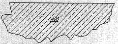
도 8a는 본 발명의 바람직한 실시형태에 따라 웨이퍼 세정 후의 기판을 나타낸 도면;8A shows a substrate after wafer cleaning in accordance with a preferred embodiment of the present invention;
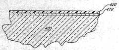
도 8b는 본 발명의 바람직한 실시형태에 따라 실리콘 산화물층의 형성 후의 도 8a의 기판을 나타낸 도면;8B illustrates the substrate of FIG. 8A after formation of a silicon oxide layer in accordance with a preferred embodiment of the present invention;
도 8c는 본 발명의 바람직한 실시형태에 따라 도 8B의 실리콘 산화물층 위에 형성된 질화 실리콘층을 나타낸 도면;8C illustrates a silicon nitride layer formed over the silicon oxide layer of FIG. 8B in accordance with a preferred embodiment of the present invention.
도 8d는 본 발명의 바람직한 실시형태에 따라 도 8c의 질화 실리콘층 위에 후속의 질화 실리콘층의 형성에 의해 더욱 두껍게 된 도 8c의 질화 실리콘층을 나타낸 도면;FIG. 8D shows the silicon nitride layer of FIG. 8C thickened by the formation of a subsequent silicon nitride layer over the silicon nitride layer of FIG. 8C in accordance with a preferred embodiment of the present invention;
도 8e는 도 8d의 질화 실리콘층이 본 발명의 바람직한 실시형태에 따라 바람직한 두께로 형성된 후에 형성된 게이트 전극을 나타낸 도면;8E illustrates a gate electrode formed after the silicon nitride layer of FIG. 8D is formed to a desired thickness in accordance with a preferred embodiment of the present invention;
도 9는 본 발명의 소정의 바람직한 실시형태에 따라 배취 반응기 내에 질화 실리콘을 형성하는 프로세스를 표시한 순서도;9 is a flow chart illustrating a process for forming silicon nitride in a batch reactor in accordance with certain preferred embodiments of the present invention.
도 10은 본 발명의 소정의 바람직한 실시형태에 따라 증착된 질화 실리콘층의 두께 및 굴절률(RI)을 나타낸 그래프;10 is a graph showing the thickness and refractive index (RI) of a silicon nitride layer deposited according to certain preferred embodiments of the present invention;
도 11은 본 발명의 소정의 바람직한 실시형태에 따라 4가지 상이한 질화반응조건을 이용해서 배취 반응기 내에서 증착된 실리콘층의 두께를 나타낸 그래프.FIG. 11 is a graph showing the thickness of a silicon layer deposited in a batch reactor using four different nitriding conditions in accordance with certain preferred embodiments of the present invention. FIG.
이하, 도면을 참조해서 설명을 행하며, 도면에 있어서 동일한 부호는 동일한 부분을 나타낸다.Hereinafter, a description will be given with reference to the drawings, in which like reference numerals designate like parts.
바람직한desirable배취Batch 반응기 Reactor
도 1 내지 도 6은 네덜란드의 빌토벤(Bilthoven)에 소재한 ASM International N.V.사로부터 상품명 Advance 412™ 또는 A412™으로 시판되고 있는 예시적인 배취 반응기의 상이한 두 버전을 도시하고 있다. 도시된 반응기는 효과적인 가열 및 적재 수순에 대한 이점을 지니는 수직로형(vertical furnace type)의 반응기이지만, 당업자라면 본 명세서에 개시된 원리 및 이점은 다른 형태의 반응기에 대해서도 적용될 것임을 이해할 수 있을 것이다.1-6 show two different versions of an exemplary batch reactor marketed under the trade names Advance 412 ™ or A412 ™ from ASM International N.V., Bilthoven, The Netherlands. The reactor shown is a vertical furnace type reactor with the advantages of effective heating and loading procedures, but one of ordinary skill in the art will appreciate that the principles and advantages disclosed herein will apply to other types of reactors as well.
도 1을 참조하면, 가스 주입기를 지닌 예시적인 길이가 긴 로의 개략적 측면단면도가 도시되어 있다. 프로세스 관 혹은 챔버(526)는 바람직하게는 가열소자(도시 생략)에 의해 둘러싸여 있다. 반응공간(529)의 외주의 한계를 규정하는 라이너(528)는 바람직하게는 프로세스 챔버(526) 내부에 설치되어 있다. 바람직하게는, 프로세스 챔버(526)의 하부에서는 웨이퍼 적재물(550)이 도어(530)에 의해 프로세스 챔버(526)에 반입 및 반출될 수 있다. 전구체 공급원 가스는 가스 주입기(540)를 통해, 바람직하게는 가스공급도관(544)을 개재해서 주입된다. 가스 주입기(540)에는 실질적으로 웨이퍼 적재물(550)의 높이에 걸쳐서 뻗어 있는 구멍(548)의 패턴이 형성되어 있다. 단, 가스 주입기(540)의 구멍(548)으로부터 반응공간(529)으로 가스가 먼저 도입되기 때문에, 가스가 경유해서 이동하는 가스 주입기(540) 등의 가스전달장치의 내부는 반응공간(529)의 일부는 아니고, 어떤 의미에서 반응공간(529)의 외부이다. 따라서, 반응공간(529)은 가스 주입기(540) 등의 가스전달장치가 차지하는 용적을 제외하고 프로세스 챔버(526)의 내부 용적을 포함한다.1, there is shown a schematic side cross-sectional view of an exemplary long furnace with a gas injector. Process tube or
바람직한 실시형태에 있어서, 프로세스 챔버(526)의 내부에는, 가스가 일반 적으로 위쪽 방향(552)으로 흐르고, 이어서 반응공간(529)으로부터 프로세스 챔버(526)와 라이너(528) 사이의 배기 공간(554)을 통해서 제거되고, 이때 가스는 펌프(도시 생략)에 연결된 배기관(558)으로 아래쪽 방향(556)으로 흐른다. 가스 주입기(540)는 바람직하게는 반응공간(529)의 전체 높이에 걸쳐 프로세스 챔버(526) 내부에 프로세스 가스를 분포시킨다. 가스 주입기(540) 자체는 가스의 흐름에 대한 규제로서 작용하므로, 도관(544)에 가까운 구멍(548)이 도관(544)으로부터 먼 이들 구멍(548)보다 반응 공간 속으로 더욱 가스를 주입하는 경향이 있다. 바람직하게는, 구멍(548)을 통한 가스 흐름의 차이에 대한 이러한 경향은 도관(544)으로부터 떨어져서 위치함에 따라 구멍(548) 간의 거리를 감소시킴으로써(즉, 구멍(548)의 밀도를 증가시킴으로써) 어느 정도 보상될 수 있다. 다른 실시형태에 있어서, 구멍(548)을 만드는 개별의 구멍의 크기는 도관(544)으로부터의 거리를 증대시킴으로써 증가될 수 있고, 또는 도관(544)으로부터의 거리가 증가함에 따라 구멍(548)의 크기를 증가시키는 동시에 구멍(548) 간의 거리도 감소시킬 수 있다. 그러나, 유리하게는, 바람직한 실시형태는 구멍(548)을 포함하고 있는 가스 주입기(540)의 측면의 표면적을 최소화하도록 일정 크기의 구멍(548)으로 예시되어있다.In a preferred embodiment, inside the
반응속도는 전형적으로 압력증가에 따라 증가하므로, 주입기(540)는 가스 주입기의 내압을 감소시키도록 설계되어, 주입기 내의 기상 반응의 감소를 초래하도록 하는 것이 유리하다. 이러한 감소된 압력은 가스 주입기(540)의 높이에 걸쳐 가스의 열등한 분포를 초래할 수도 있는 한편, 주입기(540)의 높이를 횡단하는 구 멍(548)의 분포는 가스분포의 균일성을 향상시키도록 선택된다.Since the reaction rate typically increases with increasing pressure, it is advantageous for the
본 발명의 예시된 하나의 실시형태에 따른 가스 주입기(540)는 도 2에 도시되어 있다. 가스 주입기(540)는 바람직하게는 두 개의 가스 주입기 부분(541), (542)을 포함하고, 이들은 각각 개별의 가스공급 도관 연결부(545), (546)를 구비하고 있다. 제 1 부분(541)은 반응공간(529)의 하부 용적(도 1) 속으로 가스를 주입하고, 제 2 부분(542)은 반응공간(529)의 상부 용적(도 1) 속으로 가스를 주입한다. 이들 부분(541), (542)은 결합부(549), (551)에 의해 연결되어 있다. 가스 주입기(540)에는 해당 가스 주입기(540)의 상단부를 챔버(526)(도 1) 내부의 훅 지지부에 고정하기 위한 훅(553)이 그의 상단부에 설치될 수 있다.
가스 주입기(540)에는 웨이퍼 적재물(550)(도 1)의 높이(560)(도 1) 넘어로 실질적으로 뻗어 있는 구멍(548)의 패턴이 형성되어 있다. 구멍의 총 단면적은 바람직하게는 적어도 약 30 ㎟이다. 각 구멍(548)의 직경은 바람직하게는 약 1 ㎜ 이상, 더욱 바람직하게는 약 2.5 ㎜ 내지 3.5 ㎜, 가장 바람직하게는 약 3 ㎜이다. 도 2에 표시된 예시적인 실시형태에 있어서, 가스 주입기(540)는 약 282 ㎟의 총 구멍 단면적에 대해 총 40개의 구멍을 지니고 있다. 더욱 일반적으로, 구멍(548)의 총 단면적은 바람직하게는 약 30 ㎟ 이상, 더욱 바람직하게는 약 196 ㎟ 내지 385 ㎟이다.The
도 3을 참조하면, 가스 주입기(540)의 각 부분(541) 및 (542)은 가스 주입기(540)를 통해 소스 가스의 전도에 이용가능한 내부 횡단면적(564) 및 (562)을 각각 지닌다. 바람직하게는, 내부 횡단면적(564) 및 (562)은 각각 적어도 약 100 ㎟ 였다. 예시된 실시형태에 있어서, 가스 주입기(540)의 각 부분(541), (542)의 횡단면적은 약 330 ㎟이다. 더욱 일반적으로는, 각 부분(541) 및 (542)의 횡단면적은 바람직하게는 약 140 ㎟ 내지 600 ㎟, 더욱 바람직하게는 약 225 ㎟ 내지 455 ㎟이다.Referring to FIG. 3, each
도 3에 표시된 단면은 프로세스 챔버(526)의 하단부속으로 가스를 주입하기 위해, 가스 주입기(540)의 하단부를 관통해서 가스 주입기 부분(541)에 형성된 1쌍의 주입구멍(548)을 통해 직선적으로 취한 것이다. 바람직하게는, 각 가스 주입기 부분에 있어서, 구멍(548)은 동일한 높이에 쌍으로 형성되어 있다. 또한, 두 개의 구멍(548)은 약 60° 내지 120°, 도면에서는 약 90°의 각도(570)를 이루는 두 방향(566), (568)으로 전구체 가스를 바람직하게 주입하여, 방사상 균일성을 향상시킨다. 게다가, 도시된 바와 같이, 가스 주입기(540)를 포함하는 관은, 바람직하게는 수평방향의 단면에서 보이는 바와 같이 장방형 형상을 지닌다. 바람직하게는, 이들 장방향 형상 면의 긴 쪽의 치수는 프로세스 챔버(526)의 중심에 대면하고 있고, 즉, 긴 쪽의 치수를 지닌 장방형 형상의 변은 프로세스 챔버(526)의 중심으로부터 방사상으로 뻗어있는 가상선과 직교하고 있다.The cross section shown in FIG. 3 is linear through a pair of injection holes 548 formed in the
바람직한 실시형태에 있어서, CVD 모드에서는, 이성분 막의 두 구성 원소를 제공하는 두 종의 전구체 소스 가스는 가스공급 도관 연결부(545), (546)(도 2)를 통해 가스 주입기(540)에 들어오기 전에 가스공급시스템(도시생략)에서 혼합된다. 가스공급시스템에서 전구체 가스의 예비혼합은 보트의 높이에 걸쳐서 주입된 가스의 균질한 조성물을 확보하는 하나의 방법이다. 그러나, 이들 가스는 예비 혼합하 지 않고도 프로세스 챔버(526)(도 1) 속으로 유입시킬 수 있다. 다른 실시형태에 있어서, 두 종의 전구체 소스 가스는 각각 그들 자체의 별도의 가스 주입기(540)(도시 생략)를 통해 주입될 수 있으므로, 이들은 반응공간(529)에 주입된 후 먼저 혼합된다. 따라서, 1개 이상의 가스 주입기(540)가 프로세스 챔버(526) 내부에 위치될 수 있는 것은 이해할 수 있을 것이다.In a preferred embodiment, in the CVD mode, two precursor source gases providing two constituent elements of the binary film enter the
유리하게는, 두 개의 가스 주입기 부분(541), (542)의 이용은 더욱 가능성의 조율을 허용한다. 상이한 가스 주입기 부분(541), (542)에 공급된 흐름은 반응공간(529) 속으로의 가스 흐름을 미세 조율하도록 상이하게 선택될 수 있다. 이것은 웨이퍼 적재물(550)의 높이(560)(도 1)에 걸쳐 전구체의 증착속도의 균일성을 향상시킬 것이다.Advantageously, the use of two
도 4를 참조하면, 프로세스 관(526)은 원격 플라즈마 발생기와 관련해서 도시되어 있다. 예시된 원격 플라즈마 유닛은 미국 매사추세츠주의 윌밍톤시에 소재한 MKS Instruments사로부터 시판되고 있는 마이크로파 라디칼 발생기(MRG)를 구비하고, 반응물의 소스는 작동 중에 유입되어 플라즈마 공동 또는 어플리케이터(582)에 결합된 마이크로파 전력 발생기(580)를 포함한다. 마이크로파 전력은 전력 발생기(580)로부터 도파관(584)을 통해 플라즈마 공동(582)에 결합된다. 반응물 소스, 바람직하게는 예시된 실시형태에서의 질소 공급원, 가장 바람직하게는, 이원자 질소가스(N2)는 작동 중에 플라즈마 공동(582)을 통해 흐르고, 플라즈마 생성물은 도관(586)에 의해 프로세스 챔버(526)로 반송된다. 도관 소재 및 길이는 바람직하 게는 당업자가 이해할 수 있는 바와 같이 N2에 재결합을 최소화하는 동시에 이온의 전달을 최소화하면서 천연 질소 종(N)의 전달을 최대화하도록 최적화되어 있다. 상기 도관은 도 1 내지 도 3에 예시된 형태의 가스 주입기로 인도될 수 있거나, 프로세스 관(526)의 하부 플랜지와 같이 더욱 통상의 가스 유입구로 인도될 수 있으며, 이때, 플라즈마 생성물(및 기타 반응물)은 상기 프로세스 관으로부터 위쪽으로 흘러 기판 표면을 횡단해서 확산된다.Referring to FIG. 4,
원격 MRG 유닛의 사용은 바람직한 실시형태의 펄스화된 실리콘 전구체 처리에 특히 적용될 수 있다. 대부분의 배취 프로세스와 달리, 바람직한 실시형태의 질화(nitridation) 단계(또는 기타 화합물 형성 단계)는 동력학적 방식에 있어서 자체 제한 프로세스이므로, 프로세스 챔버(526) 내에서의 라디칼 분포의 균일성은 중요하지 않다. 과반응(over-reaction)은 결과적인 견해로부터의 관심사는 아니다. 그럼에도 불구하고, 라디칼 분포의 불균일성은 질화 과정을 연장시킬 것이기 때문에 불리하고, 이때의 질화 반응은 프로세스 챔버(526) 내의 수직 위치마다 각 웨이퍼에 걸친 완전한 질화를 확보하도록 장시간 동안 수행될 것이다. 또한, 균일성 논쟁은 별도로 하고, 각 웨이퍼에 도달하도록 프로세스 챔버(526) 내에서 플라즈마 공동(582)으로부터 프로세스 챔버(526)까지 횡단하는 거리는 재결합을 일으키는 도중에 충돌에 연유한 비교적 낮은 라디칼 생존을 초래한다.The use of a remote MRG unit is particularly applicable to the pulsed silicon precursor treatment of the preferred embodiment. Unlike most batch processes, the nitriding step (or other compound formation step) of the preferred embodiment is a self limiting process in a kinetic manner, so the uniformity of radical distribution within the
도 5를 참조하면, 원위치 플라즈마 공급원(590)은 웨이퍼(550)를 가로질러 라디칼의 분포를 향상시키기 위해 프로세스 챔버(526) 내에 설치될 수 있다. 바람 직하게는, 플라즈마 공급원은 프로세스 챔버(526)(도 1)의 높이의 약 절반 이상 뻗어 있고, 더욱 바람직하게는 프로세스 챔버(526) 내에서 웨이퍼 적재물(550)의 높이의 적어도 약 90% 뻗어 있다.Referring to FIG. 5, an in
다음에, 도 6을 참조하면, 플라즈마 공급원(590)은 예를 들어 석영 또는 더욱 바람직하게는 사파이어로 형성된 절연성 슬리브(594) 내에 밀봉된 예를 들어 구리로 형성된 전도체 코일(592)을 포함한다. 선택적으로, 예를 들어, 철 또는 페라이트로 형성된 도전성 코어(596)도 포함된다. 절연성 슬리브(594)에 의해 규정된 용적(도 1)은 바람직하게는 절연성 슬리브(594) 내에서의 플라즈마 발생을 피하기 위해 배기된다.Next, referring to FIG. 6, the
작동 시, 코일에 전류가 인가된다. 용이하게 이용가능한 고주파(RF) 전원, 예를 들어 13.56 MHz은 이 목적을 위해 채용될 수 있다. 절연성 슬리브(594)의 외부지만 프로세스 챔버(526)(도 1)의 내부에 있는 플라즈마 공급원(590)을 둘러싸고 있는 프로세스 가스는 플라즈마 공급원(590)을 둘러싸는 환형상물 내에서 점화된다. 웨이퍼(550)에 대해 인접하기 때문에, 원격 플라즈마 발생기를 사용하는 것에 비해서 낮은 전력을 이용할 수 있다. 웨이퍼를 가로지르는 분포의 대칭성은 작동중에 웨이퍼 보트를 회전시킴으로써 제공될 수 있다.In operation, a current is applied to the coil. A readily available high frequency (RF) power source, for example 13.56 MHz, can be employed for this purpose. Process gas outside the insulating
바람직한 실리콘 전구체Preferred Silicon Precursors
실란은 바람직하게는 실리콘 전구체로서 이용된다. 실란은 모노실란(SiH4), 폴리실란 및 클로로실란(SiH4-nCln, 여기서 n = 1 내지 4)으로 이루어진 군으로부터 선택될 수 있다.Silanes are preferably used as silicon precursors. The silane may be selected from the group consisting of monosilane (SiH4 ), polysilane and chlorosilane (SiH4-n Cln , where n = 1 to 4).
바람직하게는, 폴리실란은 후술하는 실리콘층을 형성하기 위한 실리콘 전구체로서 이용된다. 본 명세서에서 이용되는 바와 같이, "폴리실란"은 화학식 SinH2n+2(식 중, n = 2 내지 4임)를 지닌다. 바람직하게는, 폴리실란은 디실란 또는 트리실란이다. 가장 바람직하게는, 폴리실란은 트리실란이다. 따라서, 본 발명은 트리실란에 의한 CVD 사이클을 이용하는 특히 바람직한 실시형태의 내용으로 기재되어 있으나, 당업자라면, 본 명세서의 개시에 비추어 기재된 프로세스의 소정의 이점이 다른 전구체 및/또는 다른 증착 기술에 의해서 얻어질 수 있는 것임을 이해할 것이다.Preferably, polysilane is used as a silicon precursor for forming the silicon layer mentioned later. As used herein, "polysilane" has the formula Sin H2n + 2 , wherein n = 2-4. Preferably, the polysilane is disilane or trisilane. Most preferably, the polysilane is trisilane. Thus, while the present invention has been described in the context of particularly preferred embodiments that utilize CVD cycles with trisilane, those skilled in the art will appreciate that certain advantages of the processes described in light of the disclosure herein may be achieved by other precursor and / or other deposition techniques. It will be understood that it can be obtained.
트리실란(H3SiSiH2SiH3 또는 Si3H8)은 2003년 7월 18일자 출원된 미국 특허 출원 시리얼 번호 제 10/623,482호; 2002년 2월 11일자 출원된 미국 특허 출원 번호 제10/074,564호; 및 2002년 8월 2일자 간행된 PCT 출원 공개공보 WO 02/064,853호에 개시된 바와 같은 실리콘 전구체로서 이용될 경우 실질적인 이득을 제공하고, 이들 공보에 개시된 내용은 모두 전체로서 참고로 본 명세서에 병합되어 있다. 예를 들어, 막은 실란(SiH4) 등의 다른 실리콘 전구체보다 실질적으로 낮은 온도에서 트리실란에 의해 증착될 수 있다. 게다가, 트리실란에 의한 증착 속도는 기판 재료 및 두께에 대해서 비교적 덜 민감하다. 또한, 트리실란은 극히 짧은 막 핵형성시간을 지니며, 이것은 실리콘의 국소적인 결정성 침착물의 크기를 감소시킨다. 그 결과, 증착된 실리콘 막은 박막화될 수 있는 한편, 여전히 균일하다. 게다가, 상기 막은 국소적인 실리콘 침착물의 감소된 크기로 인해 감소된 표면조도(surface roughness)를 보일 것이다.Trisilane (H3 SiSiH2 SiH3 or Si3 H8 ) is disclosed in US Patent Application Serial No. 10 / 623,482, filed Jul. 18, 2003; US Patent Application No. 10 / 074,564, filed February 11, 2002; And when used as a silicon precursor as disclosed in PCT Application Publication No. WO 02 / 064,853, issued August 2, 2002, the disclosures of which are all incorporated herein by reference in their entirety. have. For example, the film may be deposited by trisilane at a temperature substantially lower than other silicon precursors such as silane (SiH4 ). In addition, the deposition rate by trisilane is relatively less sensitive to substrate material and thickness. In addition, trisilane has an extremely short membrane nucleation time, which reduces the size of local crystalline deposits of silicon. As a result, the deposited silicon film can be thinned while still uniform. In addition, the film will exhibit reduced surface roughness due to the reduced size of the local silicon deposits.
또한, 프로세스 쓰루풋에 관해서는, 트리실란은 실란에 대해서 높은 증착속도를 나타낸다. 트리실란은 또한 실란보다 낮은 처리 온도를 이용할 수 있으므로 열적 비용을 저감시킨다.In terms of process throughput, trisilane also exhibits a high deposition rate relative to silane. Trisilane can also use lower processing temperatures than silane, thus reducing thermal costs.
따라서, 본 명세서에 기재된 증착 방법에서 트리실란을 이용하는 것은 많은 이점을 제공한다. 예를 들어, 이들 증착 방법은 균일하게 얇고 연속적인 실리콘-함유 화합물의 제조를 가능하게 한다. 이들 이점은 이어서 소자를 고수율로 제조가능하게 하고, 또한 작은 회로 치수 및/또는 높은 신뢰성을 지닌 새로운 소자의 제조도 가능하게 한다. 이들 및 기타 이점은 이하에 개시되어 있다.Thus, using trisilane in the deposition methods described herein provides many advantages. For example, these deposition methods allow for the production of uniformly thin and continuous silicon-containing compounds. These advantages then allow the device to be manufactured in high yield, and also enable the manufacture of new devices with small circuit dimensions and / or high reliability. These and other advantages are disclosed below.
바람직한 공정 흐름Preferred Process Flow
이하에 더욱 상세히 설명되어 있는 바와 같이, 실리콘 함유 화합물층의 형성시, 먼저 실리콘 전구체에 기판을 폭로시킴으로써 상기 기판상에 얇은 실리콘층이 증착된다. 다음에, 실리콘층은 다른 반응성 종과 반응해서 실리콘-함유 화합물층을 형성할 수 있다. 이들 증착 및 반응의 다수의 순차적인 사이클을 수행함으로써, 실리콘 함유 화합물층을 원하는 두께로 형성할 수 있다.As described in more detail below, upon formation of a silicon-containing compound layer, a thin silicon layer is deposited on the substrate by first exposing the substrate to a silicon precursor. The silicon layer can then react with other reactive species to form a silicon-containing compound layer. By performing a number of sequential cycles of these depositions and reactions, the silicon-containing compound layer can be formed to a desired thickness.
도 7은 본 발명의 바람직한 실시형태에 따른 일반적인 공정순서를 나타낸다. 기판은 프로세스 챔버 내에 설치되고, 모든 수순 단계는 그 프로세스 챔버 내에서 원위치(제자리)에서 수행되는 것이 바람직하다. "기판"은 본 명세서에 있어서 본 발명의 바람직한 실시형태에 따라 실리콘 함유 재료가 증착되거나 적용되는 임의의 하부 면을 포함하는 통상의 의미로 사용된다. 바람직한 기판은 제한 없이 금속, 실리콘, 게르마늄, 플라스틱 및/또는 유리, 바람직하게는 실리콘 화합물(Si-O-C-H 저유전상수막을 포함) 및 실리콘 합금을 포함하는 실질적으로 임의의 재료로 제작될 수 있다. 또한, 기판은 부분적으로 제작된 집적회로에서처럼 트렌치(trench) 혹은 단차 등의 물리적 구조를 그들에 지닐 수 있다.7 shows a general process sequence according to a preferred embodiment of the present invention. The substrate is installed in the process chamber, and all steps are preferably performed in situ within the process chamber. "Substrate" is used herein in its ordinary sense, including any bottom face on which a silicon-containing material is deposited or applied in accordance with a preferred embodiment of the present invention. Preferred substrates can be made of virtually any material including, without limitation, metals, silicon, germanium, plastics and / or glass, preferably silicon compounds (including Si-O-C-H low dielectric constant films) and silicon alloys. In addition, substrates may have physical structures in them, such as trenches or steps, as in partially fabricated integrated circuits.
단계 (100)에서, 기판을 실리콘 전구체에 폭로시킴으로써 실리콘층이 기판상에 증착된다. 실리콘 전구체는 바람직하게는 실란, 더욱 바람직하게는 폴리실란, 가장 바람직하게는 트리실란이다. 실리콘 전구체는 바람직하게는 공급 가스의 형태로 혹은 공급 가스의 성분으로서 프로세스 챔버 속으로 도입된다. 공급 가스는 불활성 캐리어 가스 등의 실리콘 전구체 이외의 기체를 포함할 수 있다. 캐리어 가스는 질소, 수소, 헬륨, 아르곤, 혹은 그의 각종 배합물 등의 당업계에 공지된 캐리어 가스를 포함할 수 있다. 바람직하게는, 질소는 캐리어 가스로서 사용된다. 실리콘 전구체가 트리실란인 경우, 트리실란은 바람직하게는 트리실란 증기를 포획하도록 캐리어 가스를 사용하는 버블러에 의해 챔버속으로 도입되고, 더욱 바람직하게는, 온도제어 버블러가 이용된다.In
실리콘층의 형성시(100), 실리콘 전구체로부터의 증착은 당업자에게 공지된 각종 증착 방법에 따라 수행될 수 있지만, 본 명세서에 교시된 CVD 방법에 따라 증착을 행할 경우 최대의 이익이 얻어진다. 개시된 방법은 플라즈마-증강 화학적 기상 증착(PECVD) 또는 더욱 바람직하게는, 열 CVD를 포함하는 CVD를 이용해서 실행될 수 있다.In the formation of the
증착 조건은 바람직하게는 기판이 적재된 특정 형태의 반응기에서의 처리에 적합하게 되어있다. 일반적으로, 증착조건은 가열된 기판 표면상에 실리콘 전구체를 열분해하거나 분해시키는 데 충분한 에너지를 공급하도록 설정되어 있다.Deposition conditions are preferably adapted for processing in a particular type of reactor loaded with a substrate. In general, the deposition conditions are set to provide sufficient energy to pyrolyze or decompose the silicon precursor on the heated substrate surface.
또한, 증착조건은 바람직하게는 실리콘 전구체의 반응속도가 실리콘 증착 속도에 대해서 다양한 제한이 있도록 설정되어 있다. 따라서, 고도로 균일한 온도 분포를 얻기 위한 가온 벽 반응기의 능력은 균일한 층을 형성하도록 유리하게 적용될 수 있다. 반응속도제한조건 하에서 수행된 증착은 온도 변화에 민감한 증착 속도를 지니지만, 고온 균일성을 확립하는 능력은 이 감도의 효과를 최소화한다. 게다가, 반응속도제한조건은 유리하게는 공급된 반응물 농도에 비교적 민감하지 않은 증착속도를 지닌다.In addition, the deposition conditions are preferably set such that the reaction rate of the silicon precursor has various limitations on the silicon deposition rate. Thus, the ability of the warm wall reactor to obtain a highly uniform temperature distribution can be advantageously applied to form a uniform layer. Deposition performed under rate limiting conditions has a deposition rate sensitive to temperature changes, but the ability to establish high temperature uniformity minimizes the effect of this sensitivity. In addition, the rate limiting conditions advantageously have a deposition rate that is relatively insensitive to the supplied reactant concentration.
반응속도제한요법은 비교적 저온의 이용에 의해 주로 얻어지는 것을 이해할 수 있을 것이다. 이 결과 배취로에서 바람직한 감소된 막증착속도로 된다. 큰 배취 크기 때문에, 반응속도제한요법으로 다운 시프트된 온도에 기인하는 증착 속도에서 적절한 쓰루풋이 여전히 달성될 수 있다. 유리하게는, 트리실란은 매우 저온에서 허용가능한 증착속도를 가능하게 하여, 열소모 비용을 상당히 저감시키는 것이 가능해진다. 당업자가 용이하게 이해하는 바와 같이, 임계치수의 축소에 따라 열소모 비용이 일정하게 감소되어, 확산 허용도를 감소시켜, 열처리에 대한 보다 낮은 내성을 지닌 신소재가 도입되고 있다. 이 공정은 바람직하게는 약 600℃ 이하의 온도, 더욱 바람직하게는 약 500℃의 온도, 더욱더 바람직하게는 약 300℃ 내지 약 500℃의 온도에서 가동된다.It will be appreciated that rate-limiting therapies are obtained primarily by the use of relatively low temperatures. This results in the desired reduced film deposition rate in the batch furnace. Due to the large batch size, adequate throughput can still be achieved at deposition rates due to downshifted temperatures with kinetics. Advantageously, trisilane allows for acceptable deposition rates at very low temperatures, which makes it possible to significantly reduce the heat consumption costs. As will be readily understood by those skilled in the art, as the critical dimension is reduced, the heat consumption cost is constantly reduced, thereby reducing the diffusion tolerance and introducing new materials with lower resistance to heat treatment. The process is preferably operated at a temperature of about 600 ° C. or less, more preferably at a temperature of about 500 ° C., even more preferably at a temperature of about 300 ° C. to about 500 ° C.
온도 이외에, 당업자는 동력학 요법이 실리콘 전구체의 부분압력 혹은 반응물 공급에 부분적으로 의존하는 것을 이해할 것이다. 바람직하게는, 반응속도는 반응물이 공급되는 속도보다 느리다.In addition to the temperature, those skilled in the art will understand that the kinetics regimen depends in part on the partial pressure or reactant supply of the silicon precursor. Preferably, the reaction rate is slower than the rate at which the reactants are fed.
단계 (100)에서 형성되는 막 두께는 당업계에 공지된 바와 같이 주어진 세트의 증착파라미터(예를 들어 총 압력 및 온도)에 대한 증착시간 및/또는 가스유량을 변화시킴으로써 의도한 용도에 따라 변경될 수 있다. 특정 세트의 증착조건을 위해서, 실리콘층 형성(100)에 대한 실리콘 증착 기간은 바람직하게는 얇은 실리콘층이 형성되도록 선택된다. 얇고 균일한 실리콘층을 형성함으로써, 이들 층은 균일한 실리콘 함유 화합물층의 형성을 고려해서 용이하게 충분히 반응될 수 있다. 바람직하게는, 실리콘층의 두께는 실리콘의 단층보다 두껍지만, 약 20 Å 미만, 더욱 바람직하게는, 약 10 Å 미만이다.The film thickness formed in
도 7을 계속 참조하면, 실리콘층 형성(100) 후, 임의의 과잉의 실리콘 전구체 및 부산물이 프로세스 챔버로부터 제거된다(110). 실리콘 전구체 제거(110)는 불활성 가스에 의한 프로세스 챔버의 정화 공정, 실리콘 전구체의 배기 공정 혹은 실리콘 전구체 가스의 반응성 종을 담지하는 가스에 의한 치환 공정을 포함하는 임의의 하나의 제거공정 혹은 이들을 조합한 제거공정에 의해 일어날 수 있다. 실리콘 전구체 가스 제거(110)가 정화에 의해 수행되는 경우, 프로세스 챔버는 적어도 한번 상기 챔버 내의 분위기를 교체하는 데 충분한 기간 동안 정화되는 것이 바람직하다.With continued reference to FIG. 7, after
실리콘 전구체 가스 제거(110)는 프로세스 챔버 내의 특정 반응물의 양이 해 당 챔버에 들어오는 다음 반응물과의 원치않는 부반응을 최소화하기에 충분히 낮은 레벨로 되도록 수행되는 것이 바람직하다는 것을 이해할 수 있을 것이다. 이어서, 이것은 형성되는 실리콘 함유 화합물층에 불순물의 바람직하지 않은 혼입을 최소화한다. 이러한 낮은 레벨의 반응물은 예를 들어 반응 챔버의 정화 혹은 배기 기간을 최적화함으로써 달성될 수 있다. 그러한 레벨에서, 프로세스 챔버는 특정 반응물이 실질적으로 없다고 말할 수 있다.It will be appreciated that silicon
도 7을 계속 참조하면, 실리콘 전구체 가스 제거(110) 후, 실리콘층은 실리콘 함유 화합물층을 형성하도록 반응성 종과 반응될 수 있다(120). 실리콘 함유 화합물층은 반응성 종을 프로세스 챔버 속으로 도입함으로써 형성될 수 있다. 바람직하게는, 반응조건은 예를 들어 질화 실리콘층의 형성에 대해서 본 명세서에서 더욱 상세히 설명되어 있는 바와 같이 실리콘층을 완전히 반응시키고 밑에 있는 구조에 대한 손상을 피하도록 선택된다. 반응성 종으로서는 주지된 바와 같이 질화 실리콘층 형성용의 반응성 질소 종, 또는 실리콘 산화물층 형성용의 반응성 산소 종을 포함할 수 있다. 반응성 질소 종의 예로는 (H3Si)3N(트리실릴아민), 암모니아, 원자 질소, 하이드라진 (H2N2), 하이드라조산(HN3), NF3, 이들의 혼합물, 및 이들의 불활성 가스(예를 들어, H2, N2, Ar, He)에 의한 희석물 등의 화학 종을 포함한다. 더욱 바람직하게는, 질소 라디칼 및/또는 암모니아는 후술하는 바와 같이 반응성 질소 종이다.With continued reference to FIG. 7, after silicon
도 7을 계속 참조하면, 실리콘 함유 화합물층의 형성(120) 후, 반응물 제 거(130)는 실리콘 전구체 제거(110)에 대한 전술한 방법의 어느 것을 이용해서 수행될 수 있다. 그러나, 이들 단계 (110) 및 (130)은 예를 들어 하나의 단계가 정화를 포함할 수 있는 반면 다른 단계는 배기를 포함할 수 있는 것과 같이, 정확히 동일한 방법에 의해 일어날 필요는 없다는 것을 이해할 수 있을 것이다.With continued reference to FIG. 7, after formation of the silicon-containing
따라서, 단계 (100), (110), (120) 및 (130)의 실행은 1 사이클(140)을 포함하고 기판상에 1층의 실리콘 함유 화합물을 증착시킨다. 다음에 상기 사이클(140)은 실리콘 함유 화합물층이 원하는 두께로 형성될 때까지 반복될 수 있다.Thus, execution of
증착된 실리콘 화합물층 위에 각종 다른 층이 형성될 수 있는 것을 이해할 수 있을 것이다. 예를 들어, 실리콘 화합물층이 게이트 유전체를 형성하는 질화 실리콘인 경우, 게이트 전극은 당업계에 공지된 방법에 의해 게이트 유전체 위에 형성될 수 있다.It will be appreciated that various other layers may be formed over the deposited silicon compound layer. For example, when the silicon compound layer is silicon nitride forming a gate dielectric, the gate electrode may be formed over the gate dielectric by methods known in the art.
도 8a 내지 도 8e를 참조하면, 게이트 유전체를 형성하는 데 적용되는 상기 공정의 결과가 예시적으로 표시되어 있다. 도 8a는 웨이퍼 세척 후의 기판(400)을 나타낸다. 증착 전의 웨이퍼 세척은 당업계에 공지된 그대로 및 그 밖의 각종 방법에 의해 수행될 수 있는 것을 알 수 있을 것이다. 도 8b는 증착된 층의 전기적 성능을 향상시키도록 기판(400) 상에 중간층(즉, 계면층)(410)이 형성되어 있는 것이 예시되어 있다. 중간층(410)은 예를 들어 열 혹은 화학적 산화 방법 또는 기판을 산화제에 폭로시키는 것을 포함하는 기타 방법을 포함하는(그러나 이들 방법으로 제한되지 않음) 당업계에 공지된 방법에 따라 그대로 혹은 그 밖의 개소에 형성되는 실리콘 산화물층일 수 있다. 도 8c는 중간층(410) 위에 제 1 사이클(140)(도 7)을 수행함으로써 형성된 질화 실리콘층(420)을 나타내고 있다. 도 8d는 사이클(140)(도 7)의 후속의 추가의 실행에 의해 더욱 두껍게 형성된 질화 실리콘층(420)을 예시하고 있다. 도 8e는 그 후에 형성된 게이트 전극(430)을 나타내고 있다.8A-8E, the results of the process applied to form the gate dielectric are shown by way of example. 8A shows the
일부의 실시형태에 있어서, 실리콘 함유 화합물층은 이어서 각 사이클(140)에서의 단계 (130)(도 7) 후에 또는 모든 사이클(140)을 완료한 후에 반응될 수 있는 것을 이해할 수 있을 것이다. 그 후에, 예를 들어, 반도체(예를 들어, SiGe)로서 작용하는 실리콘 함유 화합물층이 도핑될 수 있다. 다른 예에 있어서, 실리콘 옥시나이트라이드(SiOxNy)층은 산소 공급원을 도입해서 질화 실리콘을 산화시켜, 실리콘 옥시나이트라이드를 형성함으로써 질화 실리콘층으로부터 형성될 수 있다. 이러한 실리콘 옥시나이트라이드층은 도 8a 내지 도 8e를 참조해서 전술한 실리콘 산화물층 대신에 유전체층을 형성하기 위한 중간층으로서 이용될 수 있는 것을 이해할 수 있을 것이다. 실리콘 탄화 질화물(SiCxNy) 또는 실리콘 옥시카바이드(SiOxCy)는 마찬가지로 후속의 탄화, 질화 혹은 산화 단계에 의해 형성될 수 있다.In some embodiments, it will be appreciated that the silicon containing compound layer may then be reacted after step 130 (FIG. 7) in each cycle 140 or after completing all cycles 140. Thereafter, for example, a silicon-containing compound layer serving as a semiconductor (eg, SiGe) may be doped. In another example, a silicon oxynitride (SiOx Ny ) layer may be formed from the silicon nitride layer by introducing an oxygen source to oxidize silicon nitride to form silicon oxynitride. It will be appreciated that this silicon oxynitride layer can be used as an intermediate layer for forming a dielectric layer instead of the silicon oxide layer described above with reference to FIGS. 8A-8E. Silicon carbide nitride (SiCx Ny ) or silicon oxycarbide (SiOx Cy ) may likewise be formed by subsequent carbonization, nitriding or oxidation steps.
일부의 실시형태에 있어서, 상이한 실리콘 공급원이 상이한 사이클(140)(도 7)에서 사용될 수 있다. 예를 들어, 트리실란이 1 사이클에 대해서 실리콘 전구체로서 사용될 수 있고, 디실란이 다른 사이클에 대해서 사용될 수 있다. 바람직하게는, 트리실란은 사이클(140)(도 7)의 제 1 실행에 있어서 기판상에 증착된 제 1 실리콘층을 적어도 형성하는 데 이용된다. 후속의 실리콘층은 예를 들어 할로실란류(즉, 화학식 R4-XSiHx(식 중 R = Cl, Br 또는 I, X = 0 내지 3)를 지닌 실리콘 화합물) 또는 기타 실란류(SinH2n+2, 식 중 n = 1 내지 4, 단 n>2인 것이 바람직함)를 이용해서 형성될 수 있다. 또한 실리콘 전구체의 배합물이 이용될 수 있고, 예를 들어 트리실란 및 디실란은 제 1 실리콘층의 형성 후에 동시에 이용될 수 있는 것을 이해할 수 있을 것이다.In some embodiments, different silicon sources may be used in different cycles 140 (FIG. 7). For example, trisilane can be used as the silicon precursor for one cycle and disilane can be used for the other cycle. Preferably, trisilane is used to at least form the first layer of silicon deposited on the substrate in the first implementation of cycle 140 (FIG. 7). Subsequent silicon layers may be, for example, halosilanes (ie, silicon compounds having the formula R4-X SiHx (where R = Cl, Br or I, X = 0 to 3)) or other silanes (Sin) H2n+2 , wherein n = 1 to 4, preferably n> 2). It will also be appreciated that combinations of silicon precursors may be used, for example trisilane and disilane may be used simultaneously after formation of the first silicon layer.
더욱이, 각 사이클(140)마다 단계 (100)(도 7)에 대한 온도가 바람직하게는 등온이지만 다른 사이클(140)에 대해서는 변경될 수도 있음을 이해할 수 있을 것이다. 예를 들어, 실리콘층 형성(100)은 약 525 ℃ 미만, 바람직하게는 약 500 ℃ 미만, 가장 바람직하게는 약 475 ℃ 미만인 제 1 온도에서 일어날 수 있다. 바람직하게는, 다음에 상기 층은 실리콘 함유 화합물층을 형성(120)(도 7)하기 전에, 증착된 실리콘층으로부터 수소의 완전한 제거를 허용하도록 수초간 방치될 수 있다. 바람직하게는, 층의 방치 시간은 10초 이상이다. 다음에, 실리콘 함유 화합물층을 형성(120)(도 7)하기 위해, 온도는 상기 제 1 온도보다 높은 제 2 온도까지 증가시킨다. 바람직하게는, 후속의 사이클(140)(도 7)은 원하는 두께의 실리콘 함유 화합물층을 증착시키기 위해 이 제 2의 높은 온도에서 등온적으로 수행된다. 이러한 공정은 저온 및 수소 제거 기간이 기판 표면과의 계면에서의 수소함량이 낮은 막을 부여할 때, 결정성 실리콘(예를 들어, SiO2, 저유전상수 스핀의 유리재, 금속 산화물, 금속 규산염 및 금속) 이외의 기판 표면상에의 질화 실리콘 막의 증착 에 특히 유용하다. 유리하게는, 후속의 증착 사이클에 대한 보다 높은 온도는 낮은 수소 계면의 형성 후 더욱 빠른 증착을 허용하여 증가된 쓰루풋을 제공한다.Moreover, it will be appreciated that for each cycle 140 the temperature for step 100 (FIG. 7) is preferably isothermal, but may vary for other cycles 140. For example,
또한, 사이클(140)에서의 단계 (100) 내지 (130) 중의 어느 한 단계 혹은 이들의 조합을 다음의 단계로 진행하기 전에 복수회 수행할 수 있는 것도 이해할 수 있을 것이다. 예를 들어, 복수의 실리콘 전구체 펄스에 이은 각 실리콘 전구체 공급원의 제거는 실리콘층이 반응해서 실리콘 함유 화합물층을 형성하기 전에 실리콘층을 형성하도록 수행될 수 있다. 마찬가지로, 복수의 반응성 종 펄스에 이은 각 반응성 종의 제거는 다른 실리콘층을 형성하기 전에 혹은 형성하는 일 없이 실리콘층과 반응해서 실리콘 함유 화합물층을 형성하도록 수행될 수 있다.It will also be appreciated that any one of steps 100-130 or a combination thereof in cycle 140 can be performed multiple times before proceeding to the next step. For example, removal of each silicon precursor source following a plurality of silicon precursor pulses may be performed to form a silicon layer before the silicon layer reacts to form a silicon containing compound layer. Likewise, removal of each reactive species following a plurality of reactive species pulses may be performed to react with the silicon layer to form a silicon-containing compound layer before or without forming another silicon layer.
질화nitrification실리콘막의Silicon film 증착 deposition
도 9는 특히 트리실란(즉, 실리콘층을 형성가능함)과 반응하기 위한 라디칼의 이용에 대한 소정의 양상에 있어서 질화 실리콘층 증착 공정 및 실리콘 화합물층 형성 공정을 예시하고 있다.9 illustrates a silicon nitride layer deposition process and a silicon compound layer formation process, particularly in certain aspects of the use of radicals to react with trisilane (ie, capable of forming a silicon layer).
도 9를 참조하면, 트리실란을 흐르게 함으로써 실리콘층이 먼저 증착된다(690). 언급된 바와 같이, 공정 조건은 동력학 방식에서의 증착을 위해 구성되어 있다. 이 공정은 약 600℃ 이하의 온도, 더욱 바람직하게는 약 500℃ 이하, 더욱 더 바람직하게는, 약 400 내지 45O℃의 온도에서 가동되는 것이 바람직하다. 또한, 반응물 공급 혹은 트리실란의 부분압력은 동력학 방식에서의 증착을 유지하도록 충분히 낮은 레벨로 설정된다. 반응속도가 반응물이 공급되는 속도보다 느린 한, 적절하게 조율된 배취로(이 배취로에서는 균일한 온도가 유지될 수 있음)의 균 일성은 우수하다. 이 점에 대해서는 문헌 Sze,VLSITECHNOLOGY, pp. 240-41(1988)를 참조하면 되고, 이 문헌에 개시된 내용은 참조로 본 명세서에 병합된다. 예시된 배취 반응기에 있어서, 프로세스 압력은 약 10 Torr 이하, 더욱 바람직하게는 약 1 Torr 이하에서 유지된다. 반응속도제한증착을 유지하기 위해서, 트리실란은 바람직하게는 적어도 약 100 sccm 미만, 더욱 바람직하게는, 적어도 약 20 sccm 미만의 트리실란으로 공급된다. 이 트리실란은 전형적으로 N2, H2, Ar 또는 He 등의 비반응성 혹은 불활성 가스의 유량에 의해 희석된다. 따라서, 트리실란 부분압력은 바람직하게는 약 10 mTorr 미만, 바람직하게는, 약 3-4 mTorr이다. 바람직하게는, 트리실란 단계(690)는 약 30 내지 120초의 기간을 지닌다. 바람직하게는, 증착 단계(690)에서 약 3 내지 30 Å의 실리콘이 증착되고, 더욱 바람직하게는 약 3 내지 8 Å, 가장 바람직하게는 약 4 내지 5 Å으로 증착된다.Referring to FIG. 9, a silicon layer is first deposited 690 by flowing trisilane. As mentioned, the process conditions are configured for deposition in a kinetic manner. The process is preferably operated at a temperature of about 600 ° C. or less, more preferably about 500 ° C. or less, even more preferably about 400 to 45 ° C. In addition, the partial pressure of the reactant feed or trisilane is set at a sufficiently low level to maintain deposition in a kinetic manner. As long as the reaction rate is slower than the rate at which the reactants are fed, the uniformity of the properly tuned batch furnace (whereby uniform temperature can be maintained) is good. For this point, see Sze,VLSITECHNOLOGY , pp. 240-41 (1988), the disclosures of which are incorporated herein by reference. In the illustrated batch reactor, the process pressure is maintained at about 10 Torr or less, more preferably about 1 Torr or less. In order to maintain rate-limiting deposition, trisilane is preferably fed to trisilane of at least less than about 100 sccm, more preferably at least about 20 sccm. This trisilane is typically diluted by the flow rate of non-reactive or inert gas such as N2 , H2 , Ar or He. Thus, the trisilane partial pressure is preferably less than about 10 mTorr, preferably about 3-4 mTorr. Preferably,
바람직하게는, 증착된 실리콘층 두께의 두께는 후술하는 단계 694에서 질화 반응 조건에 의거해서 선택된다. 이것은 실리콘층의 질화 반응 동안 원자 질소가 실리콘층을 통해 밑에 있는 실리콘 기판 속으로 확산될 수 있기 때문이다. 이 질소 확산의 깊이는 당업계에 공지된 바와 같이 계측될 수 있고, 질화온도 및 질화 기간을 포함한 각종 처리 조건과 관련된다. 따라서, 주어진 세트의 처리 조건에 대해서, 원자 질소는 가능하다면 실리콘층을 통해서 질화 포화 깊이라 불리는 특정 깊이까지 확산될 것이다. 질화가 약 1분 미만 동안 일어날 경우, 질화 포화 깊이는 단기간의 질화 포화 깊이를 의미할 수 있다.Preferably, the thickness of the deposited silicon layer thickness is selected based on the nitriding reaction conditions in
밑에 있는 기판의 질화는 이론적으로 예상되는 것보다 열등한 유전체 성질을 지닌 질화 실리콘층을 초래하는 것으로 밝혀졌다. 따라서, 증착된 질화 실리콘막의 유전체 성질을 향상시키기 위해서, 밑에 있는 기판의 질화는 바람직하게는 질화 포화 깊이와 동일하게 혹은 그보다 크게 기판 위에 형성된 제 1 실리코층을 증착함으로써 최소화된다. 계속해서 증착된 층은 전형적으로 이 제 1 실리콘층 위에 증착되는 결과로서 질화 포화 깊이보다 기판으로부터 더욱 이간될 것이다. 그 결과, 제 1 층 이후에 증착된 실리콘층의 두께는 질화 포화 깊이와 동일 혹은 그 이하인 것이 바람직하다.Nitriding of underlying substrates has been shown to result in silicon nitride layers with inferior dielectric properties than would be expected in theory. Thus, to improve the dielectric properties of the deposited silicon nitride film, nitriding of the underlying substrate is preferably minimized by depositing a first silico layer formed on the substrate that is equal to or greater than the saturation depth of nitride. Subsequently the deposited layer will typically be spaced further from the substrate than the nitride saturation depth as a result of being deposited over this first silicon layer. As a result, the thickness of the silicon layer deposited after the first layer is preferably equal to or less than the nitride saturation depth.
그러나, 주어진 세트의 질화 조건에 대해서, 제 1 실리콘층의 형성 후, 후속 사이클에서 형성된 실리콘층은 질화 실리콘층 두께를 증가시킨 채 질화 포화 깊이가 비교적 일정하게 유지되므로 더욱 얇게 될 수 있다. 예를 들어, 제 1 실리콘층은 약 질화 포화 깊이, 예를 들어 약 8 내지 20 Å까지 증착될 수 있고, 후속의 층은 더욱 얇은 두께, 예를 들어, 사이클당 약 3 Å 내지 10 Å까지 증착될 수 있다. 실리콘층의 두께를 변경하는 외에, 질화 온도 및/또는 질화 기간 등의 기타 처리 조건은 실리콘층의 두께보다 깊지 않도록 변경될 수 있는 것을 이해할 수 있을 것이다.However, for a given set of nitriding conditions, after formation of the first silicon layer, the silicon layer formed in subsequent cycles may be thinner since the nitride saturation depth remains relatively constant with increasing silicon nitride layer thickness. For example, the first silicon layer can be deposited to about nitride depth of saturation, for example about 8 to 20 kPa, and subsequent layers can be deposited to a thinner thickness, for example, to about 3 kPa to 10 kPa per cycle. Can be. In addition to changing the thickness of the silicon layer, it will be appreciated that other processing conditions, such as nitriding temperature and / or nitriding period, may be changed not to be deeper than the thickness of the silicon layer.
증착 단계(690) 후에, 트리실란 흐름이 중단된다. 예시된 실시형태에 있어서, 반응기는 바람직하게는 10초 내지 5분, 가장 바람직하게는 약 20 내지 40초간 정화된다(692). 정화(692)는 기상 반응과 미립자를 원치않게 초래할 수 있는 트리실란과 후속의 라디칼 간의 상호작용을 피하게 한다. 배취 반응기에 대한 정화 유 량의 예는 N2 5 slm이다. 다른 비반응성 가스를 이용할 수 있지만, N2는 본 명세서에 기재된 질화 과정에서의 효율을 위해 특히 이점을 지닌다.After the
후속의 활성화 종이 공급되어, 증착 단계(690)에 의해 남겨진 실리콘 박층과 반응한다. 예시된 실시형태에 있어서, 질소 가스(N2)는 정화 단계(692) 전에 흐르고 있다. 따라서, 활성화 종은 N2 흐름을 단순히 계속시켜서 플라즈마 전력을 투입해서(694) 질소 라디칼을 활성화시키도록 공급될 수 있다. 당업자라면 이것이 트리실란 증착에 대해서 바람직한 매우 낮은 온도 조건하에서 비반응성인 많은 다른 반응물에 대해서도 마찬가지로 적용되지만, 실리콘층과 반응해서 실리콘 화합물을 형성하는 라디칼을 형성하도록 플라즈마 전력을 투입함으로써 활성화될 수 있는 것을 이해할 수 있을 것이다. 또한, 플라즈마 전력은 원격 플라즈마 발생기(도 4)에 대해서 혹은 원위치 플라즈마 공급원(도 6 내지 도 6)에 대해서 투입하는 것도 가능하다.Subsequent activation species is supplied to react with the thin silicon layer left by the
바람직한 실시형태에 있어서, 질소 라디칼은 고주파 전력의 인가에 의해 발생된다. 바람직한 실시형태에 있어서, 이 고주파는 ㎓ 범위이다. 일례에 있어서, 질소 라디칼은 2.45 ㎓에서 3 kW 마이크로파 전력의 인가하에 원격 마이크로파 라디칼 발생기(MRG)를 통해서 N2 1 내지 5 slm을 흐르게 함으로써 MKS Instruments로부터 MRG에서 발생된다. 임의로, 원격에서 발생된 라디칼은 1개 이상의 가스 주입기의 이용에 의해 전체 웨이퍼 적재물 상에 분포될 수 있다. 대안적으로, 질소 라디칼도 상기 로(furnace) 챔버 내부에, 바람직하게는 수직방향으로 긴 챔버의 전 체 길이에 걸쳐 발생될 수도 있다. 이것은 프로세스 관 속에서의 고주파 전력의 커플링에 의해 달성될 수 있다. 도 5 및 도 6의 실시형태에 있어서, 이 커플링은 프로세스 챔버(529)(도 1) 속으로 삽입된 코일(592)을 통해서 일어난다. 상기 언급된 바와 같이, 코일(592)은 바람직하게는 전기적 절연성 재료의 보호성 슬리브(594) 안에 놓이고, 이 슬리브(594)는 바람직하게는 해당 슬리브(594) 내부에서의 플라즈마의 발생을 피하기 위해 약 100 mTorr 이하의 압력까지 배기한다.In a preferred embodiment, the nitrogen radicals are generated by the application of high frequency power. In a preferred embodiment, this high frequency is in the Hz range. In one example, nitrogen radicals are generated in MRG from MKS Instruments by flowing N2 1 to 5 slm through a remote microwave radical generator (MRG) under application of 3 kW microwave power at 2.45 kW. Optionally, the radicals generated remotely can be distributed over the entire wafer load by the use of one or more gas injectors. Alternatively, nitrogen radicals may also be generated inside the furnace chamber, preferably over the entire length of the chamber, which is preferably long in the vertical direction. This can be achieved by coupling high frequency power in the process tube. In the embodiment of FIGS. 5 and 6, this coupling takes place through a
라디칼 반응 단계(694) 동안, 압력은 전형적으로 약 1 Torr이다. N2 가스로부터 발생된 N 라디칼에 대해서, 예를 들어, 질화 시간은 전형적으로 5 내지 10 분이다. 증착 단계(690)에 의해 형성된 실리콘의 두께에 따라, 형성된 실리콘 화합물(이 경우 질화물)의 두께는 바람직하게는 약 5 내지 40 Å, 더욱 바람직하게는, 약 5 내지 11 Å, 가장 바람직하게는, 약 5 내지 7 Å이다.During the
바람직하게는, 실리콘층의 질화반응이 종결되어, 실리콘층과 반응성 질소 종과의 반응에서 실질적으로 완전한 화학량론으로 된다. 이러한 완전한 반응은 더 적은 불순물 혼입, 더 치밀한 막, 및 향상된 두께 제어와 스텝 커버리지(step coverage)를 허용한다. 또한, 퇴적된 질화 실리콘층은 향상된 절연성을 지니고, 통상의 절연성 박막보다 두껍게 될 수 있고, 확산 장벽으로서 이들 증착층의 유효성을 증가시킬 수 있다.Preferably, the nitriding reaction of the silicon layer is terminated, resulting in substantially complete stoichiometry in the reaction of the silicon layer with the reactive nitrogen species. This complete reaction allows for less impurity incorporation, denser film, and improved thickness control and step coverage. In addition, the deposited silicon nitride layers have improved insulation, can be thicker than conventional insulating thin films, and can increase the effectiveness of these deposited layers as diffusion barriers.
화합물 실리콘층을 형성하기 위한 얇은 실리콘층의 완전한 반응 후, 플라즈마 전력을 오프상태로 절환한다(696). N2 가스의 경우, N2를 계속 흐르게 하면서 플라즈마 전력을 오프상태로 절환함으로써 정화를 유도하고, 라디칼은 전력 투입 없이 신속하게 사멸되므로, 임의의 후속의 트리실란 단계(690)에 의한 반응은 용이하게 피할 수 있게 된다.After complete reaction of the thin silicon layer to form the compound silicon layer, the plasma power is switched off (696). In the case of N2 gas, purge is induced by switching plasma power off while continuing to flow N2 , and radicals are quickly killed without powering up, so that the reaction by any
임의로, 단계 (690) 내지 (696)은 원하는 횟수만큼 많이 반복할 수 있고(698), 이때 각 사이클에서는 단계(696)에서 라디칼에 의해 신속하고 충분히 반응될 수 있도록 충분히 얇게 실리콘층을 증착시킨다(690). 1.5분의 트리실란 펄스에 대해서, 5 내지 6 Å 질화물의 막 두께가 실리콘 증착 및 질화반응의 1 사이클에서 작성된다. Optionally, steps 690-696 can be repeated as many times as desired (698), where each cycle deposits a layer of silicon thin enough to be reacted quickly and sufficiently by radicals in step 696 ( 690). For a 1.5 minute trisilane pulse, the film thickness of 5-6 kW nitride is created in one cycle of silicon deposition and nitriding reaction.
실리콘-화합물층의 형성(594)은 상이한 반응성 종에 대한 관심있는 원자 종이 동일한 경우에도 1개 이상의 반응성 종과 실리콘층의 반응을 포함할 수 있는 것을 이해할 수 있을 것이다. 예를 들어, 질화반응에 대해서, 질소 라디칼 유량에 부가해서 NH3 유량을 이용해서 유리한 효과가 관찰되었다. 이 NH3는 라디칼 발생기를 통해서라기 보다는 오히려 프로세스 관으로 직접 공급되었다. 비활성화 NH3가 500℃ 이하의 온도에 실리콘과 거의 반응하지 않더라도, 질소 라디칼에 대한 비활성화된 NH3의 첨가에 의해 더욱 완전히 질화된 비정질 실리콘층으로 되는 것은 주지되어 있다. 이론에 의해 제한되는 것을 원하는 일 없이, 원격 플라즈마 발생기로부터의 질소 라디칼은 프로세스 챔버 내에서 암모니아를 활성화시키는 것으로 여겨진다. 이에 대해서, N 라디칼은 단독으로 약간 실리콘이 풍부한 질화 실리콘 막을 남긴다. 흥미롭게도, 실제로 원격 MRG를 통해 제공된 암모니아는 N 라디칼 단독에 비해서도 질화 반응 효과를 감소시킨다.It will be appreciated that the
도 10은 네덜란드의 빌토벤에 소재한 ASM International N.V.사로부터의 배취 A412™ 반응기에서의 실험결과를 예시하며, 여기서, 기판은 약 435℃에서 유지되고, 웨이퍼 보트는 5 rpm에서 회전되었다. 반응속도제한 증착조건이 설정되었다. 1.5 분의 실리콘 증착 펄스에 있어서, 트리실란은 반응기의 바닥에서 입구를 통해 제공되어 약 3.3 mTorr의 트리실란 부분압력을 발생하였다. N2는 5 slm의 속도로 MRG를 통해서 제공되었다. 트리실란 흐름이 중단되고 약 30 초간 정화된 후, 원격 플라즈마 전력이 약 10분 동안 3,000 W의 레벨로 투입된다. 또한, NH3 1 slm의 흐름(즉, 유량)은 프로세스 챔버의 바닥을 통해 제공되었다. 질화 반응 단계 동안, 반응 챔버 내의 압력은 전형적으로 1 Torr이다. 50회의 사이클을 수행하여 약 257 Å의 두께를 지닌 질화 실리콘층을 형성하였다.FIG. 10 illustrates the results of an experiment in a batch A412 ™ reactor from ASM International NV, Biltöven, The Netherlands, where the substrate was maintained at about 435 ° C. and the wafer boat was rotated at 5 rpm. Reaction rate limiting deposition conditions were set. For a 1.5 minute silicon deposition pulse, trisilane was provided through the inlet at the bottom of the reactor to generate a trisilane partial pressure of about 3.3 mTorr. N2 was provided through MRG at a rate of 5 slm. After the trisilane flow is stopped and purged for about 30 seconds, remote plasma power is applied at a level of 3,000 W for about 10 minutes. In addition, a flow (ie flow rate) of NH3 1 slm was provided through the bottom of the process chamber. During the nitriding reaction step, the pressure in the reaction chamber is typically 1 Torr. Fifty cycles were performed to form a silicon nitride layer with a thickness of about 257 kPa.
질소 라디칼의 흐름은 트리실란의 흐름과 교대로 인가된다. 질소 라디칼이 트리실란과 동시에 흐르게 될 경우, 기상 반응은 미립자 및 불균일한 막의 원치 않는 형성을 초래하는 경향이 있다. NH3의 흐름은 가령 있다 하더라도 트리실란의 흐름과 교대로 적용될 수 있거나 또는 연속 방식으로 적용될 수 있으므로, NH3도 트리실란 펄스 동안 흐르게 된다. 언급된 바와 같이, N2와 NH3는 플라즈마 전력이 오프 상태일 경우(정화단계 및 실리콘 증착 단계) 비활성화되므로, 가스는 플라즈마 전력 부재시 바람직한 온도 조건하에서 매우 많이 반응하지 않게 되어, 압력 변동의 회피 등과 같은 이점이 가스의 일정한 공급에 의해 얻어질 수 있다.The flow of nitrogen radicals is applied alternately with the flow of trisilane. If nitrogen radicals are to flow simultaneously with trisilane, gas phase reactions tend to result in unwanted formation of particulates and non-uniform membranes. The NH3 flow may, for example, be alternating with the flow of the trisilane, or may be applied in a continuous fashion, so that NH3 also flows during the trisilane pulse. As mentioned, N2 and NH3 are deactivated when the plasma power is off (purification step and silicon deposition step), so that the gas does not react very much under desirable temperature conditions in the absence of plasma power, thereby avoiding pressure fluctuations, etc. The same advantage can be obtained by the constant supply of gas.
실험에 있어서 모든 가스는 수직 방향 반응기의 하부를 통해 제공되고 그 정상부로부터 배기되는 한편, 다른 주입 구성에 의해 이점이 얻어질 수 있는 본 발명의 개시내용에 비추어 이해될 것이다. 임의로, 프로세스 가스는 가스주입관 또는 복수의 구멍 주입구(도 2 내지 도 3)를 통해서 주입되어 전체 배취에 걸쳐서 균일성이 개선될 수도 있다. 트리실란이 이러한 주입기를 통해 제공될 경우, 트리실란 펄스 동안 캐리어 가스로서, 질화(또는 기타 반응) 펄스 동안 반응물(원격 활성화되거나 또는 제자리에 활성화되거나 간에)로서, 그리고 트리실란과 질소 펄스 간의 정화 가스로서 작용하는 N2도 동일한 주입기를 통해 제공될 수 있다. 바람직한 실시형태의 저온하에, 암모니아도 주입기를 통해서 혹은 하부의 입구를 통해서 동시에 혹은 간헐적으로(플라즈마 전력에 의해) 제공될 수 있다.In the experiment all gas will be provided through the bottom of the vertical reactor and evacuated from the top, while it will be understood in light of the present disclosure that benefits can be obtained by other injection configurations. Optionally, the process gas may be injected through a gas inlet tube or a plurality of hole inlets (FIGS. 2-3) to improve uniformity throughout the batch. When trisilane is provided through such an injector, as a carrier gas during the trisilane pulse, as a reactant (remotely activated or in situ) during the nitriding (or other reaction) pulse, and a purge gas between the trisilane and nitrogen pulses N2 , which acts as, can also be provided through the same injector. Under the low temperature of the preferred embodiment, ammonia can also be provided simultaneously or intermittently (by plasma power) through the injector or through the lower inlet.
상기 언급한 바와 같이, 상기 프로세스는 질화막 증착 프로세스를 일례로서 이용해서 설명하였지만, 실리콘 탄화물, 실리콘 산화물, 실리콘 옥시나이트라이드 및 실리콘 게르마늄 층 등의 기타 실리콘 화합물층이 이 방법으로 증착될 수 있는 것은 명백할 것이다. 이러한 실시형태에 있어서, 트리실란 단계로부터 증착된 실리콘 막은 연속하는 트리실란 펄스 사이에서 탄화, 산화, 옥시질화 또는 게르마늄 전구체에의 폭로가 수행된다. 예를 들어, 실리콘 산화물도 질소 공급원을 도입하는 것보다 오히려 실리콘 함유 화합물층의 형성(120)(도 7) 동안 산소 공급원을 도입함으로써 형성될 수 있다. 산소 공급원으로는 원자 산소, 물, 오존, 일산화 질 소 및 아산화 질소 등을 포함한 당업계에 공지된 산화제를 포함할 수 있지만, 이들로 제한되는 것은 아니다.As mentioned above, the process has been described using the nitride film deposition process as an example, but it will be apparent that other silicon compound layers such as silicon carbide, silicon oxide, silicon oxynitride and silicon germanium layers can be deposited in this manner. will be. In this embodiment, the silicon film deposited from the trisilane step is subjected to carbonization, oxidation, oxynitride or exposure to the germanium precursor between successive trisilane pulses. For example, silicon oxide may also be formed by introducing an oxygen source during formation 120 (FIG. 7) of the silicon-containing compound layer rather than introducing a nitrogen source. Oxygen sources may include, but are not limited to, oxidants known in the art, including atomic oxygen, water, ozone, nitrogen monoxide, nitrous oxide, and the like.
당업자라면 당업계에 공지된 배취 반응기에 대한 또는 배취 반응기의 작동 방법에 대한 추가의 변형을 적용하여 이 프로세스의 성능을 향상시킬 수 있는 것을 이해할 수 있을 것이다. 예를 들어, 홀더 보트 혹은 링 보트를 이용해서 각 웨이퍼에 대한 막 증착의 균일성을 향상시키는 것도 가능하다.Those skilled in the art will appreciate that further modifications to the batch reactors known in the art or to the method of operation of the batch reactors may be applied to improve the performance of this process. For example, it is also possible to improve the uniformity of the film deposition on each wafer by using a holder boat or a ring boat.
실리콘 함유Silicone-containing화합물층의Compound layer 증착 deposition
바람직하게는, 바람직한 실시형태에 의한 바람직한 실리콘 함유 화합물 막은 해당 막의 표면에 대해서 고도로 균일한 두께를 지닌다. 막 두께 균일성은 다점 두께 측정을 행함으로써, 예를 들어, 타원편광 또는 횡단측량에 의해 각종 두께 측정치를 평균해서 평균 두께를 구하고, rms 두께 가변도를 구함으로써 결정하는 것이 바람직하다. 주어진 표면적에 대한 비교를 가능하게 하기 위해, 결과는 rms 두께 가변도를 평균두께로 나누고, 100을 곱해서 그 결과를 백분율로서 표현하도록 산출한 백분율 불균일성으로서 표현될 수 있다. 바람직하게는, 두께 불균일성은 약 20% 이하, 더욱 바람직하게는 약 10% 이하, 더욱 더 바람직하게는 약 5% 이하, 가장 바람직하게는 약 2% 이하이다.Preferably, the preferred silicon-containing compound film according to the preferred embodiment has a highly uniform thickness with respect to the surface of the film. The film thickness uniformity is preferably determined by performing a multi-point thickness measurement, for example, averaging various thickness measurements by elliptical polarization or cross-sectional measurement to find the average thickness, and obtaining the rms thickness variability. To enable a comparison for a given surface area, the result can be expressed as a percentage non-uniformity calculated by dividing the rms thickness variability by the average thickness and multiplying it by 100 to express the result as a percentage. Preferably, the thickness non-uniformity is about 20% or less, more preferably about 10% or less, even more preferably about 5% or less, most preferably about 2% or less.
막 두께를 측정하는 적절한 방법은 다점 타원편광측정법을 포함한다. 막 두께를 측정하는 기기는 잘 알려져 있고 시판되고 있다. 바람직한 기기로서는 미국 캘리포니아주의 서니베일시에 소재한 Nanometrics, Inc.,로부터의 NanoSpec® 시리즈 기기를 포함한다. 실리콘 함유 화합물 막의 두께는 기판을 횡단측량하고, 적절 한 현미경 수법에 의해 두께를 측정함으로써, 가장 바람직하게는 전자현미경에 의해 구할 수도 있다. 두께가 측정되는 스팬(거리)은 막의 두께의 약 10 배로부터 실리콘 함유 화합물 막의 전체 스팬까지의 범위 내에서의 어떠한 스팬일 수도 있다. 막 두께가 상기 스팬에 걸쳐서 변화된다면, 그 두께는 평균 두께, 즉, 주어진 스팬에 걸쳐서 막의 가장 두꺼운 치수와 가장 얇은 치수의 평균수치인 것으로 간주된다.Suitable methods for measuring film thickness include multipoint ellipsometry. Instruments for measuring film thickness are well known and commercially available. Preferred instruments include NanoSpec® series instruments from Nanometrics, Inc., Sunnyvale, CA. The thickness of the silicon-containing compound film may be most preferably obtained by electron microscopy by transversing the substrate and measuring the thickness by an appropriate microscopic method. The span (distance) from which the thickness is measured may be any span within a range from about 10 times the thickness of the film to the entire span of the silicon containing compound film. If the film thickness is varied over the span, the thickness is considered to be the average thickness, ie the average value of the thickest and thinnest dimensions of the film over a given span.
본 명세서에서 사용되는 바와 같이, rms(가장 적합하게는, 평균제곱 에러의 제곱근)는 주어진 모집단의 개체에 의해 나타나는 가변도의 양을 표현하는 방식이다. 예를 들어, y 그램의 평균 중량을 지닌 대상물 군에 있어서, 그 군의 각 개체는 그 평균치로부터 (y'-y)로 표시되는 소정량만큼 상이한 중량 y'을 지닌다. rms를 산출하기 위해서, 이들 차이를 제곱하고(이들이 양수인 것을 확실하게 하기 위하여), 함께 합하여, 평균해서 평균 제곱 에러를 수득한다. 평균제곱 에러의 제곱근은 rms 가변도이다.As used herein, rms (most suitably, the square root of the mean squared error) is a way of expressing the amount of variability exhibited by an individual in a given population. For example, for a group of subjects with an average weight of y grams, each individual in that group has a weight y 'that differs from the average by a predetermined amount, expressed as (y'-y). To calculate rms, square these differences (to make sure they are positive), add them together, and average them to get the mean squared error. The square root of the mean squared error is the rms variability.
두께 균일성에 부가해서, 바람직한 실리콘 함유 화합물 막은 바람직하게는 변화된 윤곽에 대한 정합 코팅(conformal coating)을 제공한다. 정합 코팅은 가령 있다면 그 위에 놓인 구조의 곡률을 따르는 층이다. 정합 실리콘 함유 화합물 막은 바람직하게는 양호한 스텝 커버리지를 나타낸다. "스텝 커버리지"란 단차를 지닌 면 위에 놓이는 정합성 막의 두께 균일성을 의미한다. 단차를 지닌 면은 동일한 수평 방향의 평면에 배치되지 않은 2개 이상의 평행한 성분을 지니는 면이다. 스텝 커버리지는 바람직하게는 단차의 바닥부에서 막의 평균 두께를 측정하고, 이 것을 단차의 정상부에서의 평균 두께로 나누고, 100을 곱해서 그 결과를 백분율로 환산해서 표현함으로써 결정된다.In addition to thickness uniformity, the preferred silicon containing compound film preferably provides a conformal coating for the changed contour. The mating coating is, for example, a layer that conforms to the curvature of the structure overlying it. The matched silicon containing compound film preferably exhibits good step coverage. "Step coverage" means the thickness uniformity of a conformal film that lies on a stepped surface. A face with steps is a face with two or more parallel components that are not arranged in the same horizontal plane. Step coverage is preferably determined by measuring the average thickness of the film at the bottom of the step, dividing it by the average thickness at the top of the step, multiplying by 100 and expressing the result in percent terms.
바람직한 실리콘 함유 화합물 막은 비교적 높은 애스펙트비에서도 양호한 스텝 커버리지를 지닌다. "애스펙트비"란 구조체의 수평 방향 폭에 대한 단차의 수직방향 높이의 비를 의미한다. 약 4.5 내지 약 6의 범위 내의 애스펙트비에서, 바람직한 실리콘 함유 화합물 막은 약 70% 이상, 더욱 바람직하게는 80% 이상의 스텝 커버리지를 지닌다. 약 1 내지 약 4의 범위 내의 애스펙트비에서, 바람직한 실리콘 함유 화합물 막은 약 80% 이상, 더욱 바람직하게는 90% 이상의 스텝 커버리지를 지닌다. 스텝 커버리지는 바람직하게는 전술한 바와 같이 산출되지만, 측벽 두께를 고려해서 산출할 수도 있다. 예를 들어, 스텝 커버리지의 또 다른 정의는 단차의 상부 및/또는 하부에서의 평균 두께에 대한 측벽 두께의 비를 포함한다. 그러나, 다른 언급이 없는 한, 본 명세서에서 스텝 커버리지는 단차의 하부에서 실리콘 함유 화합물 막의 수평방향 부분의 평균 두께를 측정하고, 그 단차의 상부에서의 수평방향의 평균두께로 나누고 나서, 100을 곱해서 백분율로 표현함으로써 전술한 바와 같이 구한다.Preferred silicon-containing compound films have good step coverage even at relatively high aspect ratios. By "an aspect ratio" is meant the ratio of the vertical height of the step to the horizontal width of the structure. At aspect ratios within the range of about 4.5 to about 6, preferred silicon containing compound films have a step coverage of at least about 70%, more preferably at least 80%. At aspect ratios within the range of about 1 to about 4, the preferred silicon containing compound film has a step coverage of at least about 80%, more preferably at least 90%. Step coverage is preferably calculated as described above, but may be calculated in consideration of the sidewall thickness. For example, another definition of step coverage includes the ratio of sidewall thickness to average thickness at the top and / or bottom of the step. However, unless otherwise stated, step coverage herein refers to measuring the average thickness of the horizontal portion of the silicon-containing compound film at the bottom of the step, dividing by the average thickness in the horizontal direction at the top of the step, and multiplying by 100 It is calculated | required as mentioned above by expressing in percentage.
유리하게는, 바람직한 실리콘 함유 화합물 막의 표면 조도 및 두께는 약 1 제곱 마이크론(㎛2) 이상, 더욱 바람직하게는 5 ㎛2 이상, 더욱더 바람직하게는 약 10 ㎛2 이상의 표면적에 걸쳐서 유지된다. 실리콘 함유 화합물 막은 대형 기판, 예를 들어 웨이퍼의 일부 또는 전부를 커버할 수 있고, 이에 따라, 그 표면적은 약 300 ㎠ 이상, 바람직하게는 약 700 ㎠ 이상을 지닐 수 있다.Advantageously, the surface roughness and thickness of the preferred silicon containing compound film is maintained over a surface area of at least about 1 square micron (μm2 ), more preferably at least 5 μm2 , even more preferably at least about 10 μm2 . The silicon-containing compound film may cover some or all of a large substrate, for example a wafer, and thus the surface area thereof may have at least about 300 cm 2, preferably at least about 700 cm 2.
양호한 스텝 커버리지가 통상 얻어지므로, 많은 경우에 있어서, 실리콘 함유 화합물 막의 표면조도는 그것이 위에 놓인 표면의 조도와 실질적으로 동일하다. 표면조도는 대상으로 되는 표면의 1 ㎛ × 1 ㎛ 부분에 대해서 원자력 현미경(AFM)에 의해 측정된 rms 표면조도이다. 밑에 있는 기판 표면의 조도는 약 1 Å rms(원자력을 이용해서 평탄한 표면)에서 약 25 Å rms 또는 심지어 그 이상까지의 범위일 수 있다. 바람직하게는, 밑에 있는 기판 표면의 조도는 10 Å 이하, 더욱 바람직하게는 5 Å rms 이하이므로, 위에 있는 실리콘 함유 화합물 막은 견줄만한 조도를 지닌다. 주어진 조도를 지닌 밑에 있는 표면에 대해서, 그 위에 증착된 실리콘 함유 화합물 막의 표면 조도는 기판 표면조도보다 약 5 Å 이하, 더욱 바람직하게는 약 3 Å 이하, 더욱더 바람직하게는 약 2 Å 이하만큼 큰 것이 바람직하다. 예를 들어, 기판 표면조도가 약 7 Å rms인 경우, 그 위에 증착된 실리콘 함유 화합물 막의 측정된 표면조도는 바람직하게는 약 12 Å rms(7 Å + 5 Å) 이하이다. 바람직하게는, 밑에 있는 표면은 약 2 Å rms 이하의 조도를 지니고, 위에 있는 실리콘 함유 화합물 막은 약 5 Å rms 이하, 더욱 바람직하게는 약 3 Å rms 이하, 가장 바람직하게는 약 2 Å rms 이하의 측정된 표면조도를 지닌다.Since good step coverage is usually obtained, in many cases the surface roughness of the silicon-containing compound film is substantially the same as the roughness of the surface upon which it is laid. Surface roughness is rms surface roughness measured by atomic force microscopy (AFM) with respect to 1 micrometer x 1 micrometer part of the target surface. The roughness of the underlying substrate surface may range from about 1 kW rms (flat surface using atomic force) to about 25 kW rms or even more. Preferably, the roughness of the underlying substrate surface is 10 kW or less, more preferably 5 kW rms or less, so that the silicon-containing compound film on top has comparable roughness. For an underlying surface with a given roughness, the surface roughness of the silicon-containing compound film deposited thereon is about 5 GPa or less, more preferably about 3 GPa or less, even more preferably about 2 GPa or less than the substrate surface roughness. desirable. For example, when the substrate surface roughness is about 7 kPa rms, the measured surface roughness of the silicon-containing compound film deposited thereon is preferably about 12 kPa rms (7 kPa + 5 kPa) or less. Preferably, the underlying surface has roughness of about 2 kW rms or less, and the silicon-containing compound film on the top is about 5 kW rms or less, more preferably about 3 kW rms or less, most preferably about 2 kW rms or less It has a measured surface roughness.
바람직한 실시형태에 따라 형성된 실리콘 화합물층 막도 우수한 화학량론과 순도를 지닌다. 이들 이점은 트리실란이 실리콘 공급원으로서 사용되고, 활성화된 NH3 및 N2가 질소 공급원으로서 사용된 질화 실리콘층에 대해서 도 10에 표시된 결 과에서 입증된다.The silicon compound layer film formed according to the preferred embodiment also has excellent stoichiometry and purity. These advantages are demonstrated in the results shown in FIG. 10 for the silicon nitride layer where trisilane is used as the silicon source and activated NH3 and N2 are used as the nitrogen source.
질화 실리콘이 약 Si45N56, 또는 실리콘 원자당 약 1.25개의 질소원자의 비의 화학량론, 즉, 실리콘 원자당 1.33개의 질소 원자의 비를 지닌 완전하게 화학량론적인 질화 실리콘 Si3N4과 거의 동일한 것으로 판명되었으므로, 막의 분석 결과는 실질적으로 화학량론적인 질화 실리콘 막을 나타낸다. 또한, 질화 실리콘 막은 막 내의 수소 농도가 약 0.8 원자 퍼센트보다 낮은 우수한 조성 순도를 보였다. 따라서, 질화 실리콘 막의 분석 결과는 우수한 순도 및 화학량론을 지닌 막인 것을 나타냈다.Silicon nitride is almost completely equivalent to about Si45 N56 , or completely stoichiometric silicon nitride Si3 N4 with a ratio of about 1.25 nitrogen atoms per silicon atom, i.e., 1.33 nitrogen atoms per silicon atom. As it turned out to be the same, the results of the analysis of the membrane indicate a substantially stoichiometric silicon nitride membrane. In addition, the silicon nitride film exhibited excellent compositional purity with a hydrogen concentration of less than about 0.8 atomic percent in the film. Thus, the analysis results of the silicon nitride film indicated that the film had a good purity and stoichiometry.
유리하게는, 바람직한 실시형태에 따라 형성된 실리콘 함유 화합물층의 높은 정합성 및 물리적, 화학적 균일성은 통상의 프로세스에 의해 형성된 유사한 층에 대해서 향상된 물성을 지닌다. 예를 들면, 실리콘 화합물, 예를 들면, 질화 실리콘 및 실리콘 산화물의 절연층은 실리콘 화합물의 형성시 밑에 있는 기판의 반응에 부분적으로 연유하고, 또한 혼입된 수소와 같은 혼입된 불순물에 연유해서 이론적으로 예상되는 절연성보다 열악한 것으로 판명되었다. 바람직하게는, 바람직한 절연층은 혼입된 수소가 적고, 밑에 있는 기판의 반응을 최소화하여, 절연성을 향상시킨 것이다.Advantageously, the high conformability and physical and chemical uniformity of the silicon containing compound layer formed according to the preferred embodiments have improved properties for similar layers formed by conventional processes. For example, an insulating layer of a silicon compound, such as silicon nitride and silicon oxide, may theoretically be partially due to the reaction of the underlying substrate in the formation of the silicon compound, and also due to incorporated impurities such as incorporated hydrogen. It turned out to be worse than expected insulation. Preferably, the preferable insulating layer is one that contains less hydrogen and minimizes the reaction of the underlying substrate, thereby improving insulation.
특히, 본 발명에 따라 형성된 질화 실리콘 막은 실리콘 옥시나이트라이드 등의 기타 화합물이 전통적으로 호의적이었던 용도에 있어서 이용될 수 있다. 바람직하게는, 실리콘 옥시나이트라이드에 비해서 그의 상이한 재료 성질로 인해, 이러 한 적용에서의 질화 실리콘의 이용은 유전 상수가 높고 장벽 특성이 양호한 층으로 된다.In particular, the silicon nitride film formed according to the present invention can be used in applications where other compounds such as silicon oxynitride have traditionally been favorable. Preferably, due to its different material properties compared to silicon oxynitride, the use of silicon nitride in such applications results in layers with high dielectric constants and good barrier properties.
또한, 질화 실리콘층의 형성시, 처리 온도는 바람직하게는 실란을 이용하는 통상의 CVD 프로세스에 대해서 저감된다. 이와 같이, 실리콘 채널을 향한 질소 확산은 실리콘-유전체 계면에서의 질소의 양이 주의 깊게 조절되어 제한되어야만 하는 게이트 유전체 용도에 있어서 감소될 수 있다.In addition, in forming the silicon nitride layer, the processing temperature is preferably reduced for conventional CVD processes using silane. As such, nitrogen diffusion towards the silicon channel can be reduced in gate dielectric applications where the amount of nitrogen at the silicon-dielectric interface must be carefully controlled and limited.
게다가, 그의 높은 유전 상수 때문에, 질화 실리콘층은 게이트 유전체와 같이 소정의 용도에 있어서 우수할 수 있다. 이것은, 소자 임계 치수가 계속 수축함에 따라, 게이트 유전체 용도용의 SiO2 등의 통상의 재료의 이용이 실리콘 산화물의 기본적인 재료 특성으로부터 일어나는 제한에 의해 감소되기 때문이다. 양자 기계 터널링(quantum mechanical tunneling)이 유전체 층을 통한 전류 누설에 대해 우수한 기전으로 될 경우, 이들 제한은 약 15 Å 이하의 물리적 두께에 대해서 특히 중대하다. 또한, 초박형의 SiO2층은 전기적으로 활성인 도펀트 원자의 확산에 대해 만족스럽지 못한 장벽이다. 따라서, SiO2보다 유전상수가 큰 절연성 박막 재료는 누설 전류 성능을 향상시키고 또한 도펀트 원자 확산에 대해 양호한 장벽으로서 작용하기 위해서 바람직한 것으로 결정되어 있다. 게이트 유전체 용도 이외에도, 질화 실리콘막은 다수의 트랜지스터 용도에 있어서 스페이서로서 사용될 수도 있다. 이들 용도 모두에 대해서, 질화 실리콘 박막은 누설 전류 성능에 대해서 예외적인 성질을 지니는 것이 바람직하다. 또한, 게이트 유전체 용도에 대해서, 얇은 질화 실리콘 막은 바람직하게는 캐리어 이동도 전망으로부터 우수한 전기 성능을 나타내고, 이것은 낮은 계면 트랩 밀도(즉, 상부에 증착이 행해질 결정성 반도체 표면을 지닌 허용가능한 경계면)를 지니는 것을 의미한다.In addition, because of its high dielectric constant, the silicon nitride layer can be excellent in certain applications such as gate dielectrics. This is because as device critical dimensions continue to shrink, the use of conventional materials, such as SiO2 for gate dielectric applications, is reduced by the limitations arising from the basic material properties of silicon oxide. If quantum mechanical tunneling becomes a good mechanism for current leakage through the dielectric layer, these limitations are particularly significant for physical thicknesses of about 15 kΩ or less. In addition, ultra-thin SiO2 layers are an unsatisfactory barrier to the diffusion of electrically active dopant atoms. Therefore, it is determined that an insulating thin film material having a higher dielectric constant than SiO2 is preferable for improving leakage current performance and serving as a good barrier to dopant atom diffusion. In addition to gate dielectric applications, silicon nitride films may also be used as spacers in many transistor applications. For both of these applications, it is desirable for the silicon nitride thin film to have exceptional properties with respect to leakage current performance. In addition, for gate dielectric applications, thin silicon nitride films preferably exhibit good electrical performance from a carrier mobility perspective, which results in a low interfacial trap density (i.e., an acceptable interface with a crystalline semiconductor surface to be deposited thereon). It means to have.
통상의 질화 실리콘막은 질화 실리콘 자체의 높은 유전상수로 인해 이론적으로 이 필요에 적합한 것처럼 보이지만, 사실상, 통상의 CVD 프로세스에 의해 형성된 질화 실리콘막은 게이트 유전체 용도에 필요한 물리적 및 전기 특성을 나타내지 않았다. 전형적으로, 이들 막은 견줄만한 물리적 두께에서 SiO2의 것보다 단지 한계에 가깝게 양호한 누설 전류를 보인다. 이것은 일부는 막의 화학적 조성, 즉, 실리콘-질화물 층 속으로 혼입된 불순물의 존재에 기인하는 것으로 여겨진다. 수소, 탄소 및 산소 등의 원소는 이론적 예상에 부합되지 않는 막 성질의 원인이 되는 주된 불순물로 되는 것으로 여겨진다. 또한, 질화 실리콘층 자체의 "아래"에 있는 결정성 실리콘 표면과의 계면에서 질소의 의도적이지 않은 존재는 예상되는 전기 성능보다 나쁜 것에 기인하는 것으로 여겨진다. 밑에 있는 벌크 반도체 내의 이 질소는 질화 실리콘 증착 프로세스의 부산물로서 존재하는 것으로 생각된다.While conventional silicon nitride films appear to theoretically fit this need due to the high dielectric constant of silicon nitride itself, in fact, silicon nitride films formed by conventional CVD processes did not exhibit the physical and electrical properties required for gate dielectric applications. Typically, these films show a better leakage current close to the limit than that of SiO2 at comparable physical thicknesses. This is believed to be due in part to the chemical composition of the film, ie the presence of impurities incorporated into the silicon-nitride layer. Elements such as hydrogen, carbon and oxygen are believed to be the major impurities that cause film properties that do not meet theoretical expectations. It is also believed that the unintentional presence of nitrogen at the interface with the crystalline silicon surface "below" the silicon nitride layer itself is due to worse than expected electrical performance. This nitrogen in the underlying bulk semiconductor is believed to exist as a byproduct of the silicon nitride deposition process.
통상의 CVD에 의해 형성된 질화 실리콘층은 상기 개시된 분야에서 기대에 어긋나고 있으나, 상기 설명한 바와 같이 형성된 바람직한 질화 실리콘층은 예외적인 웨이퍼 내 및 웨이퍼-대-웨이퍼 두께, 원소 농도 균일성 및 낮은 혼입 원소 농도를 지닌다. 더욱이, 이들 바람직한 질화 실리콘층은 통상 형성된 질화 실리콘층보다 적은 불순물을 지니고 이론적인 예상과 더욱 일치하는 전기적 성질을 보인다. 또 한, 질화 포화 깊이와 동일하거나 큰 두께로 기판 위에 제 1 실리콘층을 증착시킴으로써, 질화 실리콘층 아래에 있는 질소의 존재를 최소화한다. 제 1 층은 이미 질화 포화 깊이보다 크거나 동일하므로, 후속의 실리콘층은 질화 포화 깊이와 동일한 두께보다 적은 두께로 증착되는 것이 유리할 수 있다. 따라서, 바람직한 실시형태에 따라 형성된 실리콘 함유 화합물 막은, 통상의 CVD 프로세스에 의해 형성된 실리콘 함유 화합물층보다 더욱 균일하고 정합성인 것에 부가해서, 우수한 유전 혹은 전기 성질을 나타낼 수도 있다.While silicon nitride layers formed by conventional CVD are against expectations in the field disclosed above, preferred silicon nitride layers formed as described above are exceptional in-wafer and wafer-to-wafer thickness, element concentration uniformity and low incorporation element concentrations. Has Moreover, these preferred silicon nitride layers have less impurities than conventionally formed silicon nitride layers and exhibit electrical properties more in line with theoretical expectations. In addition, by depositing the first silicon layer on the substrate to a thickness equal to or greater than the saturation depth of nitride, the presence of nitrogen under the silicon nitride layer is minimized. Since the first layer is already greater than or equal to the nitride saturation depth, it may be advantageous for subsequent silicon layers to be deposited to a thickness less than the same thickness as the nitride saturation depth. Therefore, the silicon-containing compound film formed according to the preferred embodiment may exhibit excellent dielectric or electrical properties in addition to being more uniform and conformable than the silicon-containing compound layer formed by a conventional CVD process.
게다가, 질화 실리콘층은 실리콘 산화물 혹은 실리콘 옥시나이트라이드 층 위에 형성되고, 나아가 집적화된 질화 실리콘 막의 전기적 성질을 더욱 향상시키는 것임을 이해할 수 있을 것이다. 따라서, 실리콘 산화물 및 실리콘 옥시나이트라이드층은 계면층(혹은 중간층)으로서 사용될 수 있다. 이들 층은 전술한 바와 같이 형성될 수 있거나, 또는 당업계에 공지된 방법에 의해 형성될 수 있다.In addition, it will be appreciated that the silicon nitride layer is formed on the silicon oxide or silicon oxynitride layer, further improving the electrical properties of the integrated silicon nitride film. Thus, the silicon oxide and silicon oxynitride layers can be used as the interfacial layer (or intermediate layer). These layers may be formed as described above, or may be formed by methods known in the art.
또, 본 발명의 방법에 따라 형성된 질화 실리콘층도 향상된 내산화성을 보인다. 향상된 내산화성은 층 형성후의 어닐링 등의 후속 단계 동안 막을 반응 챔버에 존재하는 산소 혹은 수분(예를 들어 누설 혹은 가스 순도 문제) 또는 청정실 공기 노출에 대해 덜 민감하게 한다. 유리하게는 이러한 어닐링은 불활성 분위기 조건 또는 산화분위기 하에 행할 수 있다.In addition, the silicon nitride layer formed according to the method of the present invention also shows improved oxidation resistance. Improved oxidation resistance makes the film less sensitive to oxygen or moisture (eg leakage or gas purity issues) or clean room air exposure present in the reaction chamber during subsequent steps such as annealing after layer formation. Advantageously such annealing can be carried out under inert atmosphere conditions or in an oxidizing atmosphere.
실시예Example 1 One
네덜란드의 빌토벤에 소재한 ASM International N.V.사로부터의 배취 A412™ 반응기에서 질화 실리콘층을 형성하였다. 웨이퍼의 배취를 보트에 적재하고, 이 보트를 반응 챔버 속으로 반입하여 트리실란 증착을 위해 준비하였다. 웨이퍼의 온도는, 각 웨이퍼 양단의 온도가 약 435 ℃에서 균일하도록 안정화시켰다. 상기 보트를 반응 챔버 내에서 대략 수직축을 중심으로 해서 5 rpm의 속도로 회전시켰다. 압력은 약 1.3 Torr로 설정되었다. 불활성 가스에 의해 희석된 트리실란을 3.3 mTorr의 트리실란 부분압력으로 반응 챔버 내로 1.5 분간 흘려보냈다. 이와 같이 박층의 비정질 실리콘이 얻어졌다. 이어서, 트리실란 흐름을 중단하였다. 다음에, 전력을 3000 W로 설정하고, MKS 원격 마이크로파 라디칼 발생기(MRG)를 통해 5 slm의 N2를 10분 동안 공급함으로써 질화 반응을 수행하였다. 이 사이클을 약 50회 반복하였다.A silicon nitride layer was formed in a batch A412 ™ reactor from ASM International NV, Biltöven, The Netherlands. Batches of the wafer were loaded into boats, which were loaded into the reaction chamber and prepared for trisilane deposition. The temperature of the wafer was stabilized such that the temperature across each wafer was uniform at about 435 ° C. The boat was rotated at a speed of 5 rpm about the vertical axis in the reaction chamber. The pressure was set at about 1.3 Torr. Trisilane diluted with an inert gas was flowed into the reaction chamber for 1.5 minutes at a trisilane partial pressure of 3.3 mTorr. Thus, a thin layer of amorphous silicon was obtained. The trisilane flow was then stopped. The nitriding reaction was then performed by setting the power to 3000 W and feeding 5 slm of N2 for 10 minutes through an MKS remote microwave radical generator (MRG). This cycle was repeated about 50 times.
실시예Example 2 2
질화반응 동안 마이크로파 라디칼 발생기(MRG)를 통한 5 slm의 N2의 첨가에 부가해서, 반응 챔버에 별도로 NH3를 추가로 제공한 이외에는 실시예 1의 공정을 이용해서 질화 실리콘층을 형성하였다.In addition to the addition of 5 slm of N2 through a microwave radical generator (MRG) during the nitriding reaction, the silicon nitride layer was formed using the process of Example 1, except that additional NH3 was separately provided to the reaction chamber.
증착된 막을 분석한 바, 도 10에 표시된 전술한 결과가 얻어졌다.As a result of analyzing the deposited film, the above-described results shown in FIG. 10 were obtained.
실시예Example 3 3
네덜란드의 빌토벤에 소재한 ASM International N.V.사로부터의 배취 A412™ 반응기에서 질화 실리콘층을 형성하였다. 웨이퍼의 배취를 보트에 적재하고, 수직방향으로 분리하고, 또한 주면이 수평방향으로 배향되도록 해서, 보트를 반응 챔버 속으로 반입하여 트리실란 증착을 위해 준비하였다. 웨이퍼의 온도는, 각 웨이퍼 양단의 온도가 약 435 ℃에서 균일하도록 안정화시켰다. 상기 보트를 반응 챔버 내에서 대략 수직축을 중심으로 해서 5 rpm의 속도로 회전시켰다. 처리 조건은 하기 표 1에 규정되어 있다. 상이한 질화 조건에 대해서 조사하였다: 1 - 질화 반응 없음; 2 - N2에 의한 질화 반응; 3 - N2에 의한 질화 반응 + NH3 90 sccm; 4 - N2에 의한 질화 반응 + NH3 180 sccm.모든 경우에 있어서, 트리실란 폭로 단계를 50회의 사이클 이용해서 비정질 실리콘 막을 증착하였고, 각 트리실란 폭로 단계는 정화 단계와 교대로 실시하였다. 비정질 실리콘 증착 단계 동안, 트리실란 및 N2는 제 1 다중 구멍 주입기를 통해서 주입하였다. 질화 반응 단계 동안, N2(및 NH3)는 로의 수직 높이를 넘어 뻗어 있는 1쌍의 전극을 지니고 2.45 ㎓의 주파수에서 고주파전력에 의해 구동되는 원위치 라디칼 발생기 근방에서 제 2 다중 구멍 주입기를 통해 주입되었다. 플라즈마 점화를 위해서, 고유량 및 고압을 선택해서 플라즈마의 점화를 용이하게 하였다. 후속의 플라즈마 폭로 단계 동안, 저유량 및 저압을 이용해서 라디칼의 확산길이를 증가시켜, 수직방향으로 적층된 웨이퍼 사이를 더욱 용이하게 관통할 수 있도록 하였다.A silicon nitride layer was formed in a batch A412 ™ reactor from ASM International NV, Biltöven, The Netherlands. The batch of wafers was loaded into the boat, separated in the vertical direction, and the main surface was oriented in the horizontal direction, so that the boat was brought into the reaction chamber and prepared for trisilane deposition. The temperature of the wafer was stabilized such that the temperature across each wafer was uniform at about 435 ° C. The boat was rotated at a speed of 5 rpm about the vertical axis in the reaction chamber. Treatment conditions are defined in Table 1 below. Different nitriding conditions were investigated: 1-no nitriding reaction; Nitriding by 2-N2 ; Nitriding by 3-N2 + NH3 90 sccm; Nitriding by 4-N2 + NH3 180 sccm. In all cases, the amorphous silicon film was deposited using 50 cycles of the trisilane exposure step, each trisilane exposure step being performed alternately with the purification step. During the amorphous silicon deposition step, trisilane and N2 were injected through the first multi-hole injector. During the nitrification step, N2 (and NH3 ) is injected through a second multi-hole injector near an in situ radical generator driven by high frequency power at a frequency of 2.45 kHz with a pair of electrodes extending beyond the vertical height of the furnace It became. For plasma ignition, high flow and high pressure were selected to facilitate ignition of the plasma. During the subsequent plasma exposure step, low flow rates and low pressures were used to increase the diffusion length of the radicals, making it easier to penetrate between vertically stacked wafers.
N2 유량에 대한 NH3의 첨가는 도 11에 표시한 바와 같이 질화막의 막 균일성에 대해 유익한 효과를 지녔다. 평균 막 두께의 편차는 약 1.5 Å으로 유리하게 낮았다. 이에 비해서, N2를 단독으로 이용해서 질화된 질화 실리콘 막에 대한 편차 는 약 13 Å이었고, 질화 반응 없이 증착된 비정질 실리콘 막에 대한 편차는 약 5 Å이었다.The addition of NH3 to the N2 flow rate had a beneficial effect on the film uniformity of the nitride film as shown in FIG. 11. The variation in average film thickness was advantageously low, about 1.5
NH3의 첨가는 또한 활성화된 N2단독 유량에 의한 질화반응보다도 낮은 평균 질화막 두께를 초래하였다. 평균 두께는 높은 수준의 NH3의 첨가에 의해 감소되었다. 질화막 두께가 낮을수록 막의 더욱 완전한 질화반응을 나타낼 수 있고, 또는 각 질화 반응 단계 후의 실리콘 증착에 대한 억제 시간이 길수록 이들 양자의 병합을 나타낼 수 있다.The addition of NH3 is also activated N2 The average nitride film thickness was lower than that of the nitriding reaction by a single flow rate. The average thickness was reduced by the addition of high levels of NH3 . The lower the nitride film thickness, the more complete the nitriding of the film may be exhibited, or the longer the inhibition time for silicon deposition after each nitriding reaction step, the more likely the merging of both may be.
플라즈마 질화 반응 단계 동안 N2에의 다른 첨가는 마찬가지의 유리한 효과를 지닐 수 있는 것을 이해할 수 있을 것이다. 예를 들어, Ar, H2, He 또는 이들의 혼합물을 NH3와 배합하든 배합하지 않든지 간에 N2 흐름에 첨가할 수 있다. 이론에 제한되는 일 없이, 플라즈마의 향상된 균일성, 플라즈마의 향상된 효율, 더 많은 반응성 라디칼 종의 생성 또는 더 긴 수명을 지닌 라디칼 종의 생성, 혹은 이들 효과의 조합에 의해 유리한 효과를 얻을 수 있다.It will be appreciated that other additions to N2 during the plasma nitridation step may have the same beneficial effect. For example, Ar, H2 , He or a mixture thereof can be added to the N2 stream, with or without NH3 . Without wishing to be bound by theory, advantageous effects may be obtained by improved uniformity of the plasma, improved efficiency of the plasma, generation of more reactive radical species or generation of radical species with longer lifetimes, or a combination of these effects.
따라서, 당업자라면 본 발명의 범위로부터 일탈하는 일 없이 상기 설명된 처리 공정에 대해 각종 생략, 첨가 및 변형을 행할 수 있고, 이러한 모든 변형과 변경은 첨부된 청구범위에 의해 규정된 바와 같이 본 발명의 범주 내에 들어가는 것으로 의도된 것을 이해할 수 있을 것이다.Therefore, those skilled in the art can make various omissions, additions and modifications to the above-described treatment process without departing from the scope of the present invention, and all such modifications and changes are defined by the appended claims. Understand what is intended to fall within the scope.
Claims (64)
Translated fromKoreanApplications Claiming Priority (3)
| Application Number | Priority Date | Filing Date | Title |
|---|---|---|---|
| US60506804P | 2004-08-27 | 2004-08-27 | |
| US60/605,068 | 2004-08-27 | ||
| PCT/US2005/030243WO2006026350A2 (en) | 2004-08-27 | 2005-08-25 | Low temperature silicon compound deposition |
Publications (2)
| Publication Number | Publication Date |
|---|---|
| KR20070051279A KR20070051279A (en) | 2007-05-17 |
| KR101193628B1true KR101193628B1 (en) | 2012-10-24 |
Family
ID=36000573
Family Applications (2)
| Application Number | Title | Priority Date | Filing Date |
|---|---|---|---|
| KR1020077003856AExpired - LifetimeKR101193628B1 (en) | 2004-08-27 | 2005-08-25 | Low temperature silicon compound deposition |
| KR1020050078919AWithdrawnKR20060050712A (en) | 2004-08-27 | 2005-08-26 | Remote Plasma Activated Nitride Formation |
Family Applications After (1)
| Application Number | Title | Priority Date | Filing Date |
|---|---|---|---|
| KR1020050078919AWithdrawnKR20060050712A (en) | 2004-08-27 | 2005-08-26 | Remote Plasma Activated Nitride Formation |
Country Status (5)
| Country | Link |
|---|---|
| US (1) | US7629270B2 (en) |
| JP (2) | JP4685104B2 (en) |
| KR (2) | KR101193628B1 (en) |
| TW (1) | TW200618109A (en) |
| WO (1) | WO2006026350A2 (en) |
Cited By (1)
| Publication number | Priority date | Publication date | Assignee | Title |
|---|---|---|---|---|
| KR20150104037A (en)* | 2014-03-04 | 2015-09-14 | 가부시키가이샤 히다치 고쿠사이 덴키 | Method of manufacturing semiconductor device, substrate processing apparatus, and program |
Families Citing this family (108)
| Publication number | Priority date | Publication date | Assignee | Title |
|---|---|---|---|---|
| JP2007281082A (en)* | 2006-04-04 | 2007-10-25 | Tokyo Electron Ltd | Film formation method, film-forming device, and storage medium |
| US7790634B2 (en)* | 2006-05-30 | 2010-09-07 | Applied Materials, Inc | Method for depositing and curing low-k films for gapfill and conformal film applications |
| US7902080B2 (en)* | 2006-05-30 | 2011-03-08 | Applied Materials, Inc. | Deposition-plasma cure cycle process to enhance film quality of silicon dioxide |
| US20070277734A1 (en)* | 2006-05-30 | 2007-12-06 | Applied Materials, Inc. | Process chamber for dielectric gapfill |
| US7825038B2 (en)* | 2006-05-30 | 2010-11-02 | Applied Materials, Inc. | Chemical vapor deposition of high quality flow-like silicon dioxide using a silicon containing precursor and atomic oxygen |
| US8232176B2 (en)* | 2006-06-22 | 2012-07-31 | Applied Materials, Inc. | Dielectric deposition and etch back processes for bottom up gapfill |
| JP2008202107A (en)* | 2007-02-21 | 2008-09-04 | Hitachi Kokusai Electric Inc | Substrate processing equipment |
| US7745352B2 (en)* | 2007-08-27 | 2010-06-29 | Applied Materials, Inc. | Curing methods for silicon dioxide thin films deposited from alkoxysilane precursor with harp II process |
| US7867923B2 (en)* | 2007-10-22 | 2011-01-11 | Applied Materials, Inc. | High quality silicon oxide films by remote plasma CVD from disilane precursors |
| US7803722B2 (en)* | 2007-10-22 | 2010-09-28 | Applied Materials, Inc | Methods for forming a dielectric layer within trenches |
| US7943531B2 (en) | 2007-10-22 | 2011-05-17 | Applied Materials, Inc. | Methods for forming a silicon oxide layer over a substrate |
| US8357435B2 (en) | 2008-05-09 | 2013-01-22 | Applied Materials, Inc. | Flowable dielectric equipment and processes |
| US8298628B2 (en) | 2008-06-02 | 2012-10-30 | Air Products And Chemicals, Inc. | Low temperature deposition of silicon-containing films |
| JP5102393B2 (en)* | 2008-06-03 | 2012-12-19 | エア プロダクツ アンド ケミカルズ インコーポレイテッド | Low temperature deposition of silicon-containing films |
| CA2653581A1 (en)* | 2009-02-11 | 2010-08-11 | Kenneth Scott Alexander Butcher | Migration and plasma enhanced chemical vapour deposition |
| US8481433B2 (en) | 2009-03-31 | 2013-07-09 | Applied Materials, Inc. | Methods and apparatus for forming nitrogen-containing layers |
| US8980382B2 (en) | 2009-12-02 | 2015-03-17 | Applied Materials, Inc. | Oxygen-doping for non-carbon radical-component CVD films |
| US8741788B2 (en) | 2009-08-06 | 2014-06-03 | Applied Materials, Inc. | Formation of silicon oxide using non-carbon flowable CVD processes |
| US7935643B2 (en)* | 2009-08-06 | 2011-05-03 | Applied Materials, Inc. | Stress management for tensile films |
| US7989365B2 (en)* | 2009-08-18 | 2011-08-02 | Applied Materials, Inc. | Remote plasma source seasoning |
| JP5797790B2 (en)* | 2009-09-30 | 2015-10-21 | 株式会社日立国際電気 | Semiconductor device manufacturing method, substrate processing method, and substrate processing apparatus |
| JP5467007B2 (en)* | 2009-09-30 | 2014-04-09 | 株式会社日立国際電気 | Semiconductor device manufacturing method and substrate processing apparatus |
| US20110136347A1 (en)* | 2009-10-21 | 2011-06-09 | Applied Materials, Inc. | Point-of-use silylamine generation |
| US8449942B2 (en) | 2009-11-12 | 2013-05-28 | Applied Materials, Inc. | Methods of curing non-carbon flowable CVD films |
| JP5421736B2 (en)* | 2009-11-13 | 2014-02-19 | 株式会社日立国際電気 | Semiconductor device manufacturing method, substrate processing apparatus, and program |
| JP2013516763A (en) | 2009-12-30 | 2013-05-13 | アプライド マテリアルズ インコーポレイテッド | Dielectric film growth using radicals generated using a flexible nitrogen / hydrogen ratio |
| US8329262B2 (en)* | 2010-01-05 | 2012-12-11 | Applied Materials, Inc. | Dielectric film formation using inert gas excitation |
| SG182336A1 (en) | 2010-01-06 | 2012-08-30 | Applied Materials Inc | Flowable dielectric using oxide liner |
| KR101837648B1 (en) | 2010-01-07 | 2018-04-19 | 어플라이드 머티어리얼스, 인코포레이티드 | Insitu ozone cure for radicalcomponent cvd |
| US8748259B2 (en) | 2010-03-02 | 2014-06-10 | Applied Materials, Inc. | Method and apparatus for single step selective nitridation |
| JP2013521650A (en) | 2010-03-05 | 2013-06-10 | アプライド マテリアルズ インコーポレイテッド | Conformal layer by radical component CVD |
| US8236708B2 (en) | 2010-03-09 | 2012-08-07 | Applied Materials, Inc. | Reduced pattern loading using bis(diethylamino)silane (C8H22N2Si) as silicon precursor |
| US7994019B1 (en) | 2010-04-01 | 2011-08-09 | Applied Materials, Inc. | Silicon-ozone CVD with reduced pattern loading using incubation period deposition |
| US8476142B2 (en) | 2010-04-12 | 2013-07-02 | Applied Materials, Inc. | Preferential dielectric gapfill |
| US20110256734A1 (en) | 2010-04-15 | 2011-10-20 | Hausmann Dennis M | Silicon nitride films and methods |
| US9611544B2 (en) | 2010-04-15 | 2017-04-04 | Novellus Systems, Inc. | Plasma activated conformal dielectric film deposition |
| US9390909B2 (en) | 2013-11-07 | 2016-07-12 | Novellus Systems, Inc. | Soft landing nanolaminates for advanced patterning |
| US9373500B2 (en) | 2014-02-21 | 2016-06-21 | Lam Research Corporation | Plasma assisted atomic layer deposition titanium oxide for conformal encapsulation and gapfill applications |
| US9997357B2 (en) | 2010-04-15 | 2018-06-12 | Lam Research Corporation | Capped ALD films for doping fin-shaped channel regions of 3-D IC transistors |
| US9257274B2 (en) | 2010-04-15 | 2016-02-09 | Lam Research Corporation | Gapfill of variable aspect ratio features with a composite PEALD and PECVD method |
| US9892917B2 (en) | 2010-04-15 | 2018-02-13 | Lam Research Corporation | Plasma assisted atomic layer deposition of multi-layer films for patterning applications |
| US8637411B2 (en) | 2010-04-15 | 2014-01-28 | Novellus Systems, Inc. | Plasma activated conformal dielectric film deposition |
| US8524004B2 (en) | 2010-06-16 | 2013-09-03 | Applied Materials, Inc. | Loadlock batch ozone cure |
| US8318584B2 (en) | 2010-07-30 | 2012-11-27 | Applied Materials, Inc. | Oxide-rich liner layer for flowable CVD gapfill |
| US9685320B2 (en) | 2010-09-23 | 2017-06-20 | Lam Research Corporation | Methods for depositing silicon oxide |
| US7994070B1 (en)* | 2010-09-30 | 2011-08-09 | Tokyo Electron Limited | Low-temperature dielectric film formation by chemical vapor deposition |
| US9285168B2 (en) | 2010-10-05 | 2016-03-15 | Applied Materials, Inc. | Module for ozone cure and post-cure moisture treatment |
| US8664127B2 (en) | 2010-10-15 | 2014-03-04 | Applied Materials, Inc. | Two silicon-containing precursors for gapfill enhancing dielectric liner |
| US10283321B2 (en) | 2011-01-18 | 2019-05-07 | Applied Materials, Inc. | Semiconductor processing system and methods using capacitively coupled plasma |
| JP5604316B2 (en)* | 2011-01-19 | 2014-10-08 | 株式会社アルバック | Deposition method |
| US8450191B2 (en) | 2011-01-24 | 2013-05-28 | Applied Materials, Inc. | Polysilicon films by HDP-CVD |
| US8716154B2 (en) | 2011-03-04 | 2014-05-06 | Applied Materials, Inc. | Reduced pattern loading using silicon oxide multi-layers |
| US8445078B2 (en) | 2011-04-20 | 2013-05-21 | Applied Materials, Inc. | Low temperature silicon oxide conversion |
| US8466073B2 (en) | 2011-06-03 | 2013-06-18 | Applied Materials, Inc. | Capping layer for reduced outgassing |
| US9054048B2 (en) | 2011-07-05 | 2015-06-09 | Applied Materials, Inc. | NH3 containing plasma nitridation of a layer on a substrate |
| US9404178B2 (en) | 2011-07-15 | 2016-08-02 | Applied Materials, Inc. | Surface treatment and deposition for reduced outgassing |
| TW201319299A (en)* | 2011-09-13 | 2013-05-16 | Applied Materials Inc | Activated silicon precursors for low temperature plasma enhanced deposition |
| US8617989B2 (en) | 2011-09-26 | 2013-12-31 | Applied Materials, Inc. | Liner property improvement |
| US8551891B2 (en) | 2011-10-04 | 2013-10-08 | Applied Materials, Inc. | Remote plasma burn-in |
| US8592328B2 (en) | 2012-01-20 | 2013-11-26 | Novellus Systems, Inc. | Method for depositing a chlorine-free conformal sin film |
| US8889566B2 (en) | 2012-09-11 | 2014-11-18 | Applied Materials, Inc. | Low cost flowable dielectric films |
| JP6022276B2 (en)* | 2012-09-20 | 2016-11-09 | 株式会社日立国際電気 | Semiconductor device manufacturing method, substrate processing apparatus, and program |
| KR102207992B1 (en) | 2012-10-23 | 2021-01-26 | 램 리써치 코포레이션 | Sub-saturated atomic layer deposition and conformal film deposition |
| JP6538300B2 (en) | 2012-11-08 | 2019-07-03 | ノベラス・システムズ・インコーポレーテッドNovellus Systems Incorporated | Method for depositing a film on a sensitive substrate |
| SG2013083241A (en) | 2012-11-08 | 2014-06-27 | Novellus Systems Inc | Conformal film deposition for gapfill |
| US9018108B2 (en) | 2013-01-25 | 2015-04-28 | Applied Materials, Inc. | Low shrinkage dielectric films |
| US9824881B2 (en)* | 2013-03-14 | 2017-11-21 | Asm Ip Holding B.V. | Si precursors for deposition of SiN at low temperatures |
| US9564309B2 (en) | 2013-03-14 | 2017-02-07 | Asm Ip Holding B.V. | Si precursors for deposition of SiN at low temperatures |
| US20150024152A1 (en) | 2013-07-19 | 2015-01-22 | Agilent Technologies, Inc. | Metal components with inert vapor phase coating on internal surfaces |
| US10767259B2 (en) | 2013-07-19 | 2020-09-08 | Agilent Technologies, Inc. | Components with an atomic layer deposition coating and methods of producing the same |
| JP6113626B2 (en)* | 2013-10-21 | 2017-04-12 | 東京エレクトロン株式会社 | Plasma processing equipment |
| US9214334B2 (en) | 2014-02-18 | 2015-12-15 | Lam Research Corporation | High growth rate process for conformal aluminum nitride |
| US9412581B2 (en) | 2014-07-16 | 2016-08-09 | Applied Materials, Inc. | Low-K dielectric gapfill by flowable deposition |
| US9478438B2 (en) | 2014-08-20 | 2016-10-25 | Lam Research Corporation | Method and apparatus to deposit pure titanium thin film at low temperature using titanium tetraiodide precursor |
| US9478411B2 (en) | 2014-08-20 | 2016-10-25 | Lam Research Corporation | Method to tune TiOx stoichiometry using atomic layer deposited Ti film to minimize contact resistance for TiOx/Ti based MIS contact scheme for CMOS |
| US9576792B2 (en) | 2014-09-17 | 2017-02-21 | Asm Ip Holding B.V. | Deposition of SiN |
| US9214333B1 (en) | 2014-09-24 | 2015-12-15 | Lam Research Corporation | Methods and apparatuses for uniform reduction of the in-feature wet etch rate of a silicon nitride film formed by ALD |
| US9589790B2 (en) | 2014-11-24 | 2017-03-07 | Lam Research Corporation | Method of depositing ammonia free and chlorine free conformal silicon nitride film |
| US9564312B2 (en) | 2014-11-24 | 2017-02-07 | Lam Research Corporation | Selective inhibition in atomic layer deposition of silicon-containing films |
| US20160225652A1 (en) | 2015-02-03 | 2016-08-04 | Applied Materials, Inc. | Low temperature chuck for plasma processing systems |
| US10566187B2 (en) | 2015-03-20 | 2020-02-18 | Lam Research Corporation | Ultrathin atomic layer deposition film accuracy thickness control |
| US9502238B2 (en) | 2015-04-03 | 2016-11-22 | Lam Research Corporation | Deposition of conformal films by atomic layer deposition and atomic layer etch |
| US10526701B2 (en) | 2015-07-09 | 2020-01-07 | Lam Research Corporation | Multi-cycle ALD process for film uniformity and thickness profile modulation |
| JP6560924B2 (en) | 2015-07-29 | 2019-08-14 | 株式会社Kokusai Electric | Substrate processing apparatus, semiconductor device manufacturing method, and program |
| US10410857B2 (en) | 2015-08-24 | 2019-09-10 | Asm Ip Holding B.V. | Formation of SiN thin films |
| US9601693B1 (en) | 2015-09-24 | 2017-03-21 | Lam Research Corporation | Method for encapsulating a chalcogenide material |
| US10121655B2 (en) | 2015-11-20 | 2018-11-06 | Applied Materials, Inc. | Lateral plasma/radical source |
| US9773643B1 (en) | 2016-06-30 | 2017-09-26 | Lam Research Corporation | Apparatus and method for deposition and etch in gap fill |
| US10062563B2 (en) | 2016-07-01 | 2018-08-28 | Lam Research Corporation | Selective atomic layer deposition with post-dose treatment |
| US10629435B2 (en) | 2016-07-29 | 2020-04-21 | Lam Research Corporation | Doped ALD films for semiconductor patterning applications |
| US10037884B2 (en) | 2016-08-31 | 2018-07-31 | Lam Research Corporation | Selective atomic layer deposition for gapfill using sacrificial underlayer |
| US10074543B2 (en) | 2016-08-31 | 2018-09-11 | Lam Research Corporation | High dry etch rate materials for semiconductor patterning applications |
| US9865455B1 (en) | 2016-09-07 | 2018-01-09 | Lam Research Corporation | Nitride film formed by plasma-enhanced and thermal atomic layer deposition process |
| US10832908B2 (en) | 2016-11-11 | 2020-11-10 | Lam Research Corporation | Self-aligned multi-patterning process flow with ALD gapfill spacer mask |
| US10454029B2 (en) | 2016-11-11 | 2019-10-22 | Lam Research Corporation | Method for reducing the wet etch rate of a sin film without damaging the underlying substrate |
| US10134579B2 (en) | 2016-11-14 | 2018-11-20 | Lam Research Corporation | Method for high modulus ALD SiO2 spacer |
| US10269559B2 (en) | 2017-09-13 | 2019-04-23 | Lam Research Corporation | Dielectric gapfill of high aspect ratio features utilizing a sacrificial etch cap layer |
| US10170322B1 (en) | 2017-11-16 | 2019-01-01 | Taiwan Semiconductor Manufacturing Co., Ltd. | Atomic layer deposition based process for contact barrier layer |
| CN112005343B (en) | 2018-03-02 | 2025-05-06 | 朗姆研究公司 | Selective deposition using hydrolysis |
| US10971357B2 (en) | 2018-10-04 | 2021-04-06 | Applied Materials, Inc. | Thin film treatment process |
| KR102726216B1 (en) | 2019-05-01 | 2024-11-04 | 램 리써치 코포레이션 | Modulated atomic layer deposition |
| KR102830858B1 (en)* | 2019-05-23 | 2025-07-04 | 어플라이드 머티어리얼스, 인코포레이티드 | In-situ atomic layer deposition process |
| KR102837863B1 (en) | 2019-06-04 | 2025-07-23 | 램 리써치 코포레이션 | Polymeric protective liner for reactive ion etching during patterning |
| JP2022534793A (en) | 2019-06-07 | 2022-08-03 | ラム リサーチ コーポレーション | In situ control of film properties during atomic layer deposition |
| CN114207184A (en) | 2019-08-06 | 2022-03-18 | 朗姆研究公司 | Thermal Atomic Layer Deposition of Silicon-Containing Films |
| US10950428B1 (en) | 2019-08-30 | 2021-03-16 | Mattson Technology, Inc. | Method for processing a workpiece |
| CN115735261A (en) | 2020-07-28 | 2023-03-03 | 朗姆研究公司 | Impurity reduction in silicon-containing films |
| KR20220081905A (en) | 2020-12-09 | 2022-06-16 | 에이에스엠 아이피 홀딩 비.브이. | Silicon precursors for silicon silicon nitride deposition |
Citations (1)
| Publication number | Priority date | Publication date | Assignee | Title |
|---|---|---|---|---|
| WO2004009861A3 (en)* | 2002-07-19 | 2004-07-22 | Asm Inc | Method to form ultra high quality silicon-containing compound layers |
Family Cites Families (69)
| Publication number | Priority date | Publication date | Assignee | Title |
|---|---|---|---|---|
| US4363828A (en) | 1979-12-12 | 1982-12-14 | International Business Machines Corp. | Method for depositing silicon films and related materials by a glow discharge in a disiland or higher order silane gas |
| JPS57209810A (en) | 1981-06-17 | 1982-12-23 | Asahi Chem Ind Co Ltd | Preparation of silicon nitride |
| JPS5958819A (en) | 1982-09-29 | 1984-04-04 | Hitachi Ltd | Formation of thin film |
| JPS5978918A (en) | 1982-10-26 | 1984-05-08 | Mitsui Toatsu Chem Inc | Method for forming wide bandgap amorphous silicon film |
| JPS5978919A (en) | 1982-10-26 | 1984-05-08 | Mitsui Toatsu Chem Inc | Formation of amorphous silicon film |
| JPS5989407A (en) | 1982-11-15 | 1984-05-23 | Mitsui Toatsu Chem Inc | Formation of amorphous silicon film |
| JPS6043485A (en) | 1983-08-19 | 1985-03-08 | Mitsui Toatsu Chem Inc | Formation of amorphous silicon film |
| JPS61153277A (en) | 1984-12-27 | 1986-07-11 | Agency Of Ind Science & Technol | Production of thin fine crystal silicon film |
| JPH0650730B2 (en) | 1985-09-30 | 1994-06-29 | 三井東圧化学株式会社 | Method for manufacturing semiconductor thin film |
| JPS633414A (en) | 1986-06-24 | 1988-01-08 | Agency Of Ind Science & Technol | Silicon film manufacturing method |
| JP2592238B2 (en) | 1986-06-24 | 1997-03-19 | セイコー電子工業株式会社 | Method for manufacturing thin film transistor |
| US4684542A (en) | 1986-08-11 | 1987-08-04 | International Business Machines Corporation | Low pressure chemical vapor deposition of tungsten silicide |
| JP2835723B2 (en) | 1988-02-26 | 1998-12-14 | 富士通株式会社 | Capacitor and method of manufacturing capacitor |
| JPH01268064A (en) | 1988-04-20 | 1989-10-25 | Hitachi Ltd | Formation of polycrystalline silicon thin film |
| JPH02225399A (en) | 1988-11-11 | 1990-09-07 | Fujitsu Ltd | Epitaxial growth method and growth apparatus |
| JPH02155225A (en) | 1988-12-08 | 1990-06-14 | Mitsui Toatsu Chem Inc | Method of forming amorphous semiconductor thin-film |
| JP2947828B2 (en) | 1989-09-04 | 1999-09-13 | 株式会社日立製作所 | Method for manufacturing semiconductor device |
| JP2970916B2 (en)* | 1989-10-19 | 1999-11-02 | 科学技術振興事業団 | Digital CVD method |
| US5214002A (en) | 1989-10-25 | 1993-05-25 | Agency Of Industrial Science And Technology | Process for depositing a thermal CVD film of Si or Ge using a hydrogen post-treatment step and an optional hydrogen pre-treatment step |
| JPH03185817A (en) | 1989-12-15 | 1991-08-13 | Seiko Epson Corp | Method of forming semiconductor film |
| JPH03187215A (en) | 1989-12-15 | 1991-08-15 | Sharp Corp | Method for manufacturing silicon thin film |
| JP2917392B2 (en) | 1990-04-10 | 1999-07-12 | セイコーエプソン株式会社 | Method for manufacturing semiconductor device |
| US5316844A (en) | 1990-04-16 | 1994-05-31 | Hoya Electronics Corporation | Magnetic recording medium comprising an aluminum alloy substrate, now magnetic underlayers, magnetic layer, protective layer, particulate containing protective layer and lubricant layer |
| KR100209856B1 (en) | 1990-08-31 | 1999-07-15 | 가나이 쓰도무 | Method of manufacturing semiconductor device |
| JP3193402B2 (en) | 1990-08-31 | 2001-07-30 | 株式会社日立製作所 | Method for manufacturing semiconductor device |
| DE69131570T2 (en) | 1990-11-16 | 2000-02-17 | Seiko Epson Corp., Tokio/Tokyo | Method of manufacturing a thin film semiconductor device |
| US5849601A (en) | 1990-12-25 | 1998-12-15 | Semiconductor Energy Laboratory Co., Ltd. | Electro-optical device and method for manufacturing the same |
| US5356673A (en) | 1991-03-18 | 1994-10-18 | Jet Process Corporation | Evaporation system and method for gas jet deposition of thin film materials |
| JP3200863B2 (en) | 1991-04-23 | 2001-08-20 | セイコーエプソン株式会社 | Method for manufacturing semiconductor device |
| US5614257A (en) | 1991-08-09 | 1997-03-25 | Applied Materials, Inc | Low temperature, high pressure silicon deposition method |
| JP3121131B2 (en) | 1991-08-09 | 2000-12-25 | アプライド マテリアルズ インコーポレイテッド | Low temperature and high pressure silicon deposition method |
| US5695819A (en) | 1991-08-09 | 1997-12-09 | Applied Materials, Inc. | Method of enhancing step coverage of polysilicon deposits |
| JP3181357B2 (en) | 1991-08-19 | 2001-07-03 | 株式会社東芝 | Method for forming semiconductor thin film and method for manufacturing semiconductor device |
| JPH0562911A (en) | 1991-09-04 | 1993-03-12 | Fujitsu Ltd | Manufacture of semiconductor superlattice |
| US5352636A (en) | 1992-01-16 | 1994-10-04 | Applied Materials, Inc. | In situ method for cleaning silicon surface and forming layer thereon in same chamber |
| JP2740087B2 (en) | 1992-08-15 | 1998-04-15 | 株式会社東芝 | Method for manufacturing semiconductor integrated circuit device |
| DE4419074C2 (en) | 1993-06-03 | 1998-07-02 | Micron Semiconductor Inc | Method for uniformly doping polycrystalline silicon with hemispherical grain |
| US5648293A (en) | 1993-07-22 | 1997-07-15 | Nec Corporation | Method of growing an amorphous silicon film |
| US5471330A (en) | 1993-07-29 | 1995-11-28 | Honeywell Inc. | Polysilicon pixel electrode |
| JP2641385B2 (en) | 1993-09-24 | 1997-08-13 | アプライド マテリアルズ インコーポレイテッド | Film formation method |
| US6083810A (en) | 1993-11-15 | 2000-07-04 | Lucent Technologies | Integrated circuit fabrication process |
| US5656531A (en) | 1993-12-10 | 1997-08-12 | Micron Technology, Inc. | Method to form hemi-spherical grain (HSG) silicon from amorphous silicon |
| JPH07249618A (en) | 1994-03-14 | 1995-09-26 | Fujitsu Ltd | Method for manufacturing semiconductor device |
| JP3276514B2 (en)* | 1994-04-26 | 2002-04-22 | 東京エレクトロン株式会社 | Plasma processing equipment |
| US5698771A (en) | 1995-03-30 | 1997-12-16 | The United States Of America As Represented By The United States National Aeronautics And Space Administration | Varying potential silicon carbide gas sensor |
| JP3169337B2 (en) | 1995-05-30 | 2001-05-21 | キヤノン株式会社 | Photovoltaic element and method for manufacturing the same |
| US6161498A (en) | 1995-09-14 | 2000-12-19 | Tokyo Electron Limited | Plasma processing device and a method of plasma process |
| US5869389A (en) | 1996-01-18 | 1999-02-09 | Micron Technology, Inc. | Semiconductor processing method of providing a doped polysilicon layer |
| JP3109570B2 (en) | 1996-01-27 | 2000-11-20 | 株式会社半導体エネルギー研究所 | Semiconductor device manufacturing method |
| US5786027A (en) | 1996-02-14 | 1998-07-28 | Micron Technology, Inc. | Method for depositing polysilicon with discontinuous grain boundaries |
| US5789030A (en) | 1996-03-18 | 1998-08-04 | Micron Technology, Inc. | Method for depositing doped amorphous or polycrystalline silicon on a substrate |
| JPH09270421A (en) | 1996-04-01 | 1997-10-14 | Mitsubishi Electric Corp | Surface treatment apparatus and surface treatment method |
| JP2795313B2 (en) | 1996-05-08 | 1998-09-10 | 日本電気株式会社 | Capacitive element and method of manufacturing the same |
| JPH1197667A (en) | 1997-09-24 | 1999-04-09 | Sharp Corp | Method for forming ultrafine particles or ultrafine wires, and semiconductor device using ultrafine particles or ultrafine wires by this method |
| US6228181B1 (en) | 1997-10-02 | 2001-05-08 | Shigeo Yamamoto | Making epitaxial semiconductor device |
| KR100268936B1 (en) | 1997-12-16 | 2000-10-16 | 김영환 | A method of forming for quantum dot of semiconductor device |
| US6027705A (en) | 1998-01-08 | 2000-02-22 | Showa Denko K.K. | Method for producing a higher silane |
| JP3854731B2 (en) | 1998-03-30 | 2006-12-06 | シャープ株式会社 | Microstructure manufacturing method |
| KR100363083B1 (en) | 1999-01-20 | 2002-11-30 | 삼성전자 주식회사 | Hemispherical grain capacitor and forming method thereof |
| JPH11317530A (en) | 1999-02-22 | 1999-11-16 | Semiconductor Energy Lab Co Ltd | Semiconductor device |
| US6197669B1 (en) | 1999-04-15 | 2001-03-06 | Taiwan Semicondcutor Manufacturing Company | Reduction of surface defects on amorphous silicon grown by a low-temperature, high pressure LPCVD process |
| US6492711B1 (en) | 1999-06-22 | 2002-12-10 | Matsushita Electric Industrial Co., Ltd. | Heterojunction bipolar transistor and method for fabricating the same |
| JP4192353B2 (en) | 1999-09-21 | 2008-12-10 | 株式会社デンソー | Silicon carbide semiconductor device and manufacturing method thereof |
| US6337289B1 (en)* | 1999-09-24 | 2002-01-08 | Applied Materials. Inc | Method and apparatus for integrating a metal nitride film in a semiconductor device |
| US6613695B2 (en) | 2000-11-24 | 2003-09-02 | Asm America, Inc. | Surface preparation prior to deposition |
| AU2002306436A1 (en) | 2001-02-12 | 2002-10-15 | Asm America, Inc. | Improved process for deposition of semiconductor films |
| US6809370B1 (en)* | 2003-07-31 | 2004-10-26 | Texas Instruments Incorporated | High-k gate dielectric with uniform nitrogen profile and methods for making the same |
| US7132338B2 (en) | 2003-10-10 | 2006-11-07 | Applied Materials, Inc. | Methods to fabricate MOSFET devices using selective deposition process |
| DE102004039468B4 (en)* | 2004-08-14 | 2008-09-25 | R3T Gmbh Rapid Reactive Radicals Technology | Device for generating excited and / or ionized particles in a plasma |
- 2005
- 2005-08-24USUS11/212,503patent/US7629270B2/enactiveActive
- 2005-08-25KRKR1020077003856Apatent/KR101193628B1/ennot_activeExpired - Lifetime
- 2005-08-25WOPCT/US2005/030243patent/WO2006026350A2/enactiveApplication Filing
- 2005-08-25JPJP2007530121Apatent/JP4685104B2/ennot_activeExpired - Lifetime
- 2005-08-26TWTW094129189Apatent/TW200618109A/enunknown
- 2005-08-26JPJP2005245398Apatent/JP2006086521A/ennot_activeWithdrawn
- 2005-08-26KRKR1020050078919Apatent/KR20060050712A/ennot_activeWithdrawn
Patent Citations (1)
| Publication number | Priority date | Publication date | Assignee | Title |
|---|---|---|---|---|
| WO2004009861A3 (en)* | 2002-07-19 | 2004-07-22 | Asm Inc | Method to form ultra high quality silicon-containing compound layers |
Cited By (3)
| Publication number | Priority date | Publication date | Assignee | Title |
|---|---|---|---|---|
| KR20150104037A (en)* | 2014-03-04 | 2015-09-14 | 가부시키가이샤 히다치 고쿠사이 덴키 | Method of manufacturing semiconductor device, substrate processing apparatus, and program |
| KR101676558B1 (en)* | 2014-03-04 | 2016-11-15 | 가부시키가이샤 히다치 고쿠사이 덴키 | Method of manufacturing semiconductor device, substrate processing apparatus, and program |
| US9613798B2 (en) | 2014-03-04 | 2017-04-04 | Hitachi Kokusai Electric Inc. | Method of manufacturing semiconductor device, substrate processing apparatus, and recording medium |
Also Published As
| Publication number | Publication date |
|---|---|
| TW200618109A (en) | 2006-06-01 |
| WO2006026350A2 (en) | 2006-03-09 |
| KR20070051279A (en) | 2007-05-17 |
| JP2006086521A (en) | 2006-03-30 |
| JP4685104B2 (en) | 2011-05-18 |
| US7629270B2 (en) | 2009-12-08 |
| KR20060050712A (en) | 2006-05-19 |
| US20060110943A1 (en) | 2006-05-25 |
| JP2008511993A (en) | 2008-04-17 |
| WO2006026350A3 (en) | 2006-10-12 |
Similar Documents
| Publication | Publication Date | Title |
|---|---|---|
| KR101193628B1 (en) | Low temperature silicon compound deposition | |
| US7294582B2 (en) | Low temperature silicon compound deposition | |
| US7629267B2 (en) | High stress nitride film and method for formation thereof | |
| US7964513B2 (en) | Method to form ultra high quality silicon-containing compound layers | |
| KR101327923B1 (en) | Boron nitride and boron nitride-derived materials deposition method | |
| US8563090B2 (en) | Boron film interface engineering | |
| TWI748792B (en) | Method of depositing silicon nitride thin film | |
| US6867152B1 (en) | Properties of a silica thin film produced by a rapid vapor deposition (RVD) process | |
| US7202166B2 (en) | Surface preparation prior to deposition on germanium | |
| KR101442212B1 (en) | ALD of metal silicate films | |
| US20060286818A1 (en) | Method for silicon based dielectric chemical vapor deposition | |
| EP1908098A2 (en) | Uniform batch film deposition process and films so produced | |
| JP2004529489A (en) | Method of forming high dielectric constant gate insulating layer | |
| KR20030041088A (en) | System and method for improved thin dielectric films | |
| KR20070039964A (en) | Deposition of Nano-Modified Silicon Using a Single Wafer Chamber | |
| KR101046757B1 (en) | Capacitor of semiconductor device and manufacturing method thereof |
Legal Events
| Date | Code | Title | Description |
|---|---|---|---|
| PA0105 | International application | Patent event date:20070216 Patent event code:PA01051R01D Comment text:International Patent Application | |
| PG1501 | Laying open of application | ||
| A201 | Request for examination | ||
| PA0201 | Request for examination | Patent event code:PA02012R01D Patent event date:20100302 Comment text:Request for Examination of Application | |
| E902 | Notification of reason for refusal | ||
| PE0902 | Notice of grounds for rejection | Comment text:Notification of reason for refusal Patent event date:20110609 Patent event code:PE09021S01D | |
| E701 | Decision to grant or registration of patent right | ||
| PE0701 | Decision of registration | Patent event code:PE07011S01D Comment text:Decision to Grant Registration Patent event date:20120921 | |
| GRNT | Written decision to grant | ||
| PR0701 | Registration of establishment | Comment text:Registration of Establishment Patent event date:20121016 Patent event code:PR07011E01D | |
| PR1002 | Payment of registration fee | Payment date:20121017 End annual number:3 Start annual number:1 | |
| PG1601 | Publication of registration | ||
| FPAY | Annual fee payment | Payment date:20150918 Year of fee payment:4 | |
| PR1001 | Payment of annual fee | Payment date:20150918 Start annual number:4 End annual number:4 | |
| FPAY | Annual fee payment | Payment date:20160921 Year of fee payment:5 | |
| PR1001 | Payment of annual fee | Payment date:20160921 Start annual number:5 End annual number:5 | |
| FPAY | Annual fee payment | Payment date:20170919 Year of fee payment:6 | |
| PR1001 | Payment of annual fee | Payment date:20170919 Start annual number:6 End annual number:6 | |
| FPAY | Annual fee payment | Payment date:20180918 Year of fee payment:7 | |
| PR1001 | Payment of annual fee | Payment date:20180918 Start annual number:7 End annual number:7 | |
| FPAY | Annual fee payment | Payment date:20190917 Year of fee payment:8 | |
| PR1001 | Payment of annual fee | Payment date:20190917 Start annual number:8 End annual number:8 | |
| PR1001 | Payment of annual fee | Payment date:20210927 Start annual number:10 End annual number:10 | |
| PR1001 | Payment of annual fee | Payment date:20240925 Start annual number:13 End annual number:13 |