KR101189152B1 - Array substrate, liquid display panel and liquid crystal display having the same - Google Patents
Array substrate, liquid display panel and liquid crystal display having the sameDownload PDFInfo
- Publication number
- KR101189152B1 KR101189152B1KR1020050087031AKR20050087031AKR101189152B1KR 101189152 B1KR101189152 B1KR 101189152B1KR 1020050087031 AKR1020050087031 AKR 1020050087031AKR 20050087031 AKR20050087031 AKR 20050087031AKR 101189152 B1KR101189152 B1KR 101189152B1
- Authority
- KR
- South Korea
- Prior art keywords
- insulating film
- thickness
- array substrate
- gate
- liquid crystal
- Prior art date
- Legal status (The legal status is an assumption and is not a legal conclusion. Google has not performed a legal analysis and makes no representation as to the accuracy of the status listed.)
- Expired - Lifetime
Links
Images


Classifications
- G—PHYSICS
- G02—OPTICS
- G02F—OPTICAL DEVICES OR ARRANGEMENTS FOR THE CONTROL OF LIGHT BY MODIFICATION OF THE OPTICAL PROPERTIES OF THE MEDIA OF THE ELEMENTS INVOLVED THEREIN; NON-LINEAR OPTICS; FREQUENCY-CHANGING OF LIGHT; OPTICAL LOGIC ELEMENTS; OPTICAL ANALOGUE/DIGITAL CONVERTERS
- G02F1/00—Devices or arrangements for the control of the intensity, colour, phase, polarisation or direction of light arriving from an independent light source, e.g. switching, gating or modulating; Non-linear optics
- G02F1/01—Devices or arrangements for the control of the intensity, colour, phase, polarisation or direction of light arriving from an independent light source, e.g. switching, gating or modulating; Non-linear optics for the control of the intensity, phase, polarisation or colour
- G02F1/13—Devices or arrangements for the control of the intensity, colour, phase, polarisation or direction of light arriving from an independent light source, e.g. switching, gating or modulating; Non-linear optics for the control of the intensity, phase, polarisation or colour based on liquid crystals, e.g. single liquid crystal display cells
- G02F1/133—Constructional arrangements; Operation of liquid crystal cells; Circuit arrangements
- G02F1/136—Liquid crystal cells structurally associated with a semi-conducting layer or substrate, e.g. cells forming part of an integrated circuit
- G02F1/1362—Active matrix addressed cells
- G02F1/136227—Through-hole connection of the pixel electrode to the active element through an insulation layer
- G—PHYSICS
- G02—OPTICS
- G02F—OPTICAL DEVICES OR ARRANGEMENTS FOR THE CONTROL OF LIGHT BY MODIFICATION OF THE OPTICAL PROPERTIES OF THE MEDIA OF THE ELEMENTS INVOLVED THEREIN; NON-LINEAR OPTICS; FREQUENCY-CHANGING OF LIGHT; OPTICAL LOGIC ELEMENTS; OPTICAL ANALOGUE/DIGITAL CONVERTERS
- G02F1/00—Devices or arrangements for the control of the intensity, colour, phase, polarisation or direction of light arriving from an independent light source, e.g. switching, gating or modulating; Non-linear optics
- G02F1/01—Devices or arrangements for the control of the intensity, colour, phase, polarisation or direction of light arriving from an independent light source, e.g. switching, gating or modulating; Non-linear optics for the control of the intensity, phase, polarisation or colour
- G02F1/13—Devices or arrangements for the control of the intensity, colour, phase, polarisation or direction of light arriving from an independent light source, e.g. switching, gating or modulating; Non-linear optics for the control of the intensity, phase, polarisation or colour based on liquid crystals, e.g. single liquid crystal display cells
- G02F1/133—Constructional arrangements; Operation of liquid crystal cells; Circuit arrangements
- G02F1/136—Liquid crystal cells structurally associated with a semi-conducting layer or substrate, e.g. cells forming part of an integrated circuit
- G—PHYSICS
- G02—OPTICS
- G02F—OPTICAL DEVICES OR ARRANGEMENTS FOR THE CONTROL OF LIGHT BY MODIFICATION OF THE OPTICAL PROPERTIES OF THE MEDIA OF THE ELEMENTS INVOLVED THEREIN; NON-LINEAR OPTICS; FREQUENCY-CHANGING OF LIGHT; OPTICAL LOGIC ELEMENTS; OPTICAL ANALOGUE/DIGITAL CONVERTERS
- G02F1/00—Devices or arrangements for the control of the intensity, colour, phase, polarisation or direction of light arriving from an independent light source, e.g. switching, gating or modulating; Non-linear optics
- G02F1/01—Devices or arrangements for the control of the intensity, colour, phase, polarisation or direction of light arriving from an independent light source, e.g. switching, gating or modulating; Non-linear optics for the control of the intensity, phase, polarisation or colour
- G02F1/13—Devices or arrangements for the control of the intensity, colour, phase, polarisation or direction of light arriving from an independent light source, e.g. switching, gating or modulating; Non-linear optics for the control of the intensity, phase, polarisation or colour based on liquid crystals, e.g. single liquid crystal display cells
- G02F1/133—Constructional arrangements; Operation of liquid crystal cells; Circuit arrangements
- G02F1/1333—Constructional arrangements; Manufacturing methods
- G02F1/1335—Structural association of cells with optical devices, e.g. polarisers or reflectors
Landscapes
- Physics & Mathematics (AREA)
- Nonlinear Science (AREA)
- Mathematical Physics (AREA)
- Chemical & Material Sciences (AREA)
- Crystallography & Structural Chemistry (AREA)
- General Physics & Mathematics (AREA)
- Optics & Photonics (AREA)
- Engineering & Computer Science (AREA)
- Microelectronics & Electronic Packaging (AREA)
- Liquid Crystal (AREA)
- Devices For Indicating Variable Information By Combining Individual Elements (AREA)
- Thin Film Transistor (AREA)
Abstract
Translated fromKorean
Description
Translated fromKorean도 1은 본 발명의 실시예에 따른 어레이 기판의 평면도이다.1 is a plan view of an array substrate according to an embodiment of the present invention.
도 2는 도 1의 I-I' 선을 따라 절단한 단면도이다.FIG. 2 is a cross-sectional view taken along the line II ′ of FIG. 1.
도 3은 유기 절연막의 두께 편차에 따른 투과율의 변동을 나타낸 그래프이다.3 is a graph showing variation in transmittance according to thickness variation of an organic insulating layer.
도 4a는 비교예에 따른 제1 어레이 기판의 단면도이다.4A is a cross-sectional view of a first array substrate according to a comparative example.
도 4b는 도 4a의 제1 어레이 기판의 광 투과율을 나타낸 그래프이다.4B is a graph illustrating light transmittance of the first array substrate of FIG. 4A.
도 5a는 본 발명의 실시예에 따른 제2 어레이 기판의 단면도이다.5A is a cross-sectional view of a second array substrate in accordance with an embodiment of the present invention.
도 5b는 도 5a의 제2 어레이 기판의 광 투과율을 나타낸 그래프이다.FIG. 5B is a graph showing the light transmittance of the second array substrate of FIG. 5A.
도 6 내지 도 9는 도 1에 도시된 어레이 기판의 제조 방법을 설명하기 위한 공정도들이다.6 to 9 are process diagrams for describing a method of manufacturing the array substrate illustrated in FIG. 1.
도 10은 본 발명의 다른 실시예에 따른 액정표시패널의 단면도이다.10 is a cross-sectional view of a liquid crystal display panel according to another exemplary embodiment of the present invention.
도 11은 본 발명의 또 다른 실시예에 따른 액정표시장치의 분해 사시도이다.11 is an exploded perspective view of a liquid crystal display according to another exemplary embodiment of the present invention.
도 12는 본 발명의 실시예에 따라 표시 품질의 개선 효과를 나타낸 그래프이다.12 is a graph showing an effect of improving display quality according to an embodiment of the present invention.
<도면의 주요부분에 대한 부호의 설명><Description of the symbols for the main parts of the drawings>
101 : 베이스 기판102 : 게이트 절연막101
103 : 보호 절연막104 : 하부 절연막103: protective insulating film 104: lower insulating film
105 : 유기 절연막TFT : 스위칭 소자105: organic insulating film TFT: switching element
DLm-1, DLm : 소스 배선들GLn-1, GLn : 게이트 배선들DLm-1, DLm: Source Wirings GLn-1, GLn: Gate Wirings
CST : 스토리지 캐패시터L : 광CST: Storage Capacitor L: Optical
본 발명은 어레이 기판과, 이를 구비한 액정표시패널 및 액정표시장치에 관한 것으로, 보다 상세하게는 표시 품질을 향상하기 위한 어레이 기판과, 이를 구비한 액정표시패널 및 액정표시장치에 관한 것이다.The present invention relates to an array substrate, a liquid crystal display panel and a liquid crystal display device having the same, and more particularly, to an array substrate for improving display quality, and a liquid crystal display panel and a liquid crystal display device having the same.
일반적으로 어레이 기판은 제1 방향의 배열된 게이트 배선들과, 상기 제1 방향과 교차하는 제2 방향으로 배열된 복수의 소스 배선들에 의해 정의되는 복수의 화소부를 갖는다. 상기 화소부는 상기 게이트 배선과 연결된 게이트 전극과, 상기 소스 배선과 연결된 소스 전극을 갖는 스위칭 소자와, 상기 스위칭 소자의 드레인 전극과 연결되는 화소 전극을 갖는다. 상기 화소 전극은 상기 게이트 배선들과 소스 배선들에 의해 정의된 화소 영역에 형성된다.In general, an array substrate has a plurality of pixel portions defined by gate lines arranged in a first direction and a plurality of source lines arranged in a second direction crossing the first direction. The pixel portion includes a switching element having a gate electrode connected to the gate line, a source electrode connected to the source line, and a pixel electrode connected to a drain electrode of the switching element. The pixel electrode is formed in a pixel region defined by the gate lines and the source lines.
최근 고휘도의 액정표시패널을 개발하기 위해 고개구율(또는 고투과율)의 화소 구조가 개발되고 있다. 상기 고개구율의 화소 구조는 상기 화소 전극이 소스 배선 위에 오버레이 되도록 형성하여 상기 화소 전극의 형성영역을 확장시킴으로써 개구율(또는 투과율)을 향상시키는 구조이다.Recently, in order to develop a high brightness liquid crystal display panel, a high aperture ratio (or high transmittance) pixel structure has been developed. The high aperture pixel structure is formed so that the pixel electrode is overlaid on the source wiring to extend the formation region of the pixel electrode to improve the aperture ratio (or transmittance).
상기 고투과율 화소 구조를 구현하기 위해서는 상기 화소 전극과 소스 배선이 일정부분 오버레이되는 영역에서 발생되는 기생 커패시턴스를 최소화하기 위해 상기 화소 전극 및 소스 배선 사이에 두꺼운 유기 절연막이 형성된다.In order to realize the high-transmittance pixel structure, a thick organic insulating layer is formed between the pixel electrode and the source wiring to minimize parasitic capacitance generated in an area where the pixel electrode and the source wiring are partially overlaid.
상기 두껍게 형성되는 유기 절연막은 공정 특성에 의해 상기 어레이 기판에 균일한 두께로 형성되지 못한다. 이러한 유기 절연막의 두께 편차는 액정표시패널에 표시되는 영상에 붉은 얼룩 및 화이트 얼룩 등과 같은 얼룩 불량이 발생시킨다.The thick organic insulating layer may not be formed to a uniform thickness on the array substrate due to process characteristics. The thickness variation of the organic insulating layer causes uneven defects such as red spots and white spots in the image displayed on the liquid crystal display panel.
이에 본 발명의 기술적 과제는 이러한 종래의 문제점을 해결하기 위한 것으로, 본 발명의 목적은 얼룩 불량을 개선하기 위한 어레이 기판을 제공하는 것이다.Accordingly, the technical problem of the present invention is to solve such a conventional problem, and an object of the present invention is to provide an array substrate for improving the stain defect.
본 발명의 다른 목적은 상기 어레이 기판을 포함하는 액정표시패널을 제공하는 것이다.Another object of the present invention is to provide a liquid crystal display panel including the array substrate.
본 발명의 또 다른 목적은 표시 품질을 향상시키기 위한 액정표시장치를 제공하는 것이다.Another object of the present invention is to provide a liquid crystal display device for improving display quality.
상기한 본 발명의 목적을 실현하기 위한 실시예에 따른 게이트 배선들과 소스 배선들에 의해 정의된 화소 영역들로 이루어지고 각 화소 영역으로 광을 투과시키는 어레이 기판은 스위칭 소자, 화소 전극, 유기 절연막 및 하부 절연막을 포함한다. 상기 스위칭 소자는 게이트 배선과 소스 배선에 연결되어 상기 화소 영역에 형성된다. 상기 화소 전극은 상기 스위칭 소자와 전기적으로 연결된다. 상기 유기 절연막은 상기 스위칭 소자 위에 형성된다. 상기 하부 절연막은 상기 유기 절연막 아래에 형성되며, 상기 하부 절연막의 두께는 상기 광의 레드 피크 파장대에 연동된다.According to an embodiment of the present invention, an array substrate including pixel regions defined by gate lines and source lines and transmitting light to each pixel region includes a switching element, a pixel electrode, and an organic insulating layer. And a lower insulating film. The switching element is connected to the gate line and the source line and is formed in the pixel area. The pixel electrode is electrically connected to the switching element. The organic insulating film is formed on the switching element. The lower insulating film is formed under the organic insulating film, and the thickness of the lower insulating film is linked to the red peak wavelength band of the light.
상기한 본 발명의 다른 목적을 실현하기 위한 실시예에 따른 광을 이용하여 영상을 표시하는 액정표시패널은 어레이 기판 및 대향 기판을 포함한다. 상기 어레이 기판은 게이트 배선과 소스 배선에 연결된 스위칭 소자와, 상기 스위칭 소자 위에 형성된 유기 절연막 및 상기 광의 레드 피크 파장대에 연동된 두께로 상기 유기 절연막 아래에 형성된 하부 절연막을 포함한다. 상기 대향 기판은 상기 어레이 기판과 결합하여 액정층을 수용한다.A liquid crystal display panel displaying an image using light according to an embodiment for realizing another object of the present invention includes an array substrate and an opposing substrate. The array substrate includes a switching element connected to a gate line and a source line, an organic insulating layer formed on the switching element, and a lower insulating layer formed below the organic insulating layer to a thickness interlocked with the red peak wavelength band of the light. The opposite substrate is combined with the array substrate to receive a liquid crystal layer.
상기한 본 발명의 또 다른 목적을 실현하기 위한 실시예에 따른 액정표시장치는 광원 및 액정표시패널을 포함한다. 상기 광원은 광을 발생한다. 상기 액정표시패널은 게이트 배선과 소스 배선에 연결된 스위칭 소자와, 상기 스위칭 소자 위에 형성된 유기 절연막 및 상기 광의 레드 피크 파장대에 연동된 두께로 상기 유기 절연막 아래에 형성된 하부 절연막을 포함하는 어레이 기판 및 상기 어레이 기판과 결합하여 액정층을 수용하는 대향 기판을 포함한다.A liquid crystal display device according to an embodiment for realizing another object of the present invention described above includes a light source and a liquid crystal display panel. The light source generates light. The liquid crystal display panel includes an array substrate including a switching element connected to a gate wiring and a source wiring, an organic insulating layer formed on the switching element, and a lower insulating layer formed below the organic insulating layer to a thickness interlocked with the red peak wavelength band of the light. An opposing substrate is combined with the substrate to receive the liquid crystal layer.
상기한 본 발명의 목적을 실현하기 위한 실시예에 따른 게이트 배선들과 소스 배선들에 의해 정의된 화소 영역들로 이루어지고 각 화소 영역으로 광을 투과시키는 어레이 기판은 스위칭 소자, 화소 전극, 유기 절연막 및 하부 절연막을 포함한다. 상기 스위칭 소자는 게이트 배선과 소스 배선에 연결되어 상기 화소 영역에 형성된다. 상기 화소 전극은 상기 스위칭 소자와 전기적으로 연결된다. 상기 유기 절연막은 상기 스위칭 소자 위에 형성된다. 상기 하부 절연막은 상기 유기 절연막의 두께 편차에 따른 투과율 변화를 최소화시키는 두께를 갖는다.According to an embodiment of the present invention, an array substrate including pixel regions defined by gate lines and source lines and transmitting light to each pixel region includes a switching element, a pixel electrode, and an organic insulating layer. And a lower insulating film. The switching element is connected to the gate line and the source line and is formed in the pixel area. The pixel electrode is electrically connected to the switching element. The organic insulating film is formed on the switching element. The lower insulating layer has a thickness for minimizing a change in transmittance due to thickness variation of the organic insulating layer.
이러한 어레이 기판과, 이를 구비한 액정표시패널 및 액정표시장치에 의하면, 채용된 광원으로부터 발생된 광의 레드 피크 파장대에 연동하여 하부 절연막을 소정 두께로 형성함으로써 얼룩 불량을 개선하여 표시 품질을 향상시킬 수 있다.According to such an array substrate, a liquid crystal display panel and a liquid crystal display device including the same, the lower insulating film is formed to a predetermined thickness in association with the red peak wavelength band of the light generated from the light source employed to improve the display quality by improving the stain defect. have.
이하, 첨부한 도면들을 참조하여, 본 발명을 보다 상세하게 설명하고자 한다.DETAILED DESCRIPTION OF THE PREFERRED EMBODIMENTS The present invention will now be described in more detail with reference to the accompanying drawings.
도 1은 본 발명의 실시예에 따른 어레이 기판의 평면도이다.1 is a plan view of an array substrate according to an embodiment of the present invention.
도 1을 참조하면, 어레이 기판에는 복수의 게이트 배선들(GLn-1, GLn)과, 복수의 소스 배선들(DLm-1, DLm)과, 상기 게이트 배선들(GLn-1, GLn)과 소스 배선들(DLm-1, DLm)에 의해 정의된 복수의 화소부(P)들이 형성된다.Referring to FIG. 1, an array substrate includes a plurality of gate lines GLn-1 and GLn, a plurality of source lines DLm-1 and DLm, and gate lines GLn-1 and GLn and a source. A plurality of pixel portions P defined by the wirings DLm-1 and DLm are formed.
상기 게이트 배선들(GLn-1,GLn)은 제1 방향으로 배열되고, 제2 방향으로 연장된다. 상기 소스 배선들(DLm-1, DLm)은 상기 제2 방향으로 배열되고, 제1 방향으로 연장된다.The gate lines GLn-1 and GLn are arranged in a first direction and extend in a second direction. The source wirings DLm-1 and DLm are arranged in the second direction and extend in the first direction.
상기 화소부(P)는 n 번째 게이트 배선(GLn), m 번째 소스 배선(DLm), 스위칭 소자(TFT), 스토리지 캐패시터(CST) 및 화소 전극(PE)을 포함한다.The pixel portion P includes an n-th gate line GLn, an m-th source line DLm, a switching element TFT, a storage capacitor CST, and a pixel electrode PE.
상기 n 번째 게이트 배선(GLn)은 상기 화소부(P)의 구동을 제어하는 제어신호가 전달되고, 상기 m 번째 소스 배선(DLm)은 상기 화소부(P)를 구동시키는 구동 전압이 전달된다.The control signal for controlling the driving of the pixel portion P is transmitted to the n-th gate wiring GLn, and the driving voltage for driving the pixel portion P is transmitted to the m-th source wiring DLm.
상기 스위칭 소자(TFT)는 상기 n 번째 게이트 배선(GLn)에 연결된 게이트 전 극(111)과, 상기 m 번째 소스 배선(DLm)에 연결된 소스 전극(113)과, 상기 화소 전극(PE)과 콘택홀(117)을 통해서 전기적으로 연결된 드레인 전극(114)을 포함한다.The switching element TFT includes a
상기 스위칭 소자(TFT)의 구동 방식은 상기 게이트 전극(111)에 제어 신호가 입력됨에 따라 상기 소스 전극(113)으로 입력된 구동 전압을 상기 드레인 전극(114)에 연결된 화소 전극(PE)으로 전달한다.In the driving method of the switching element TFT, as a control signal is input to the
상기 스토리지 캐패시터(CST)는 스토리지 공통배선(121)과 전극 패턴(123)을 포함한다. 상기 스토리지 캐패시터(CST)는 상기 전극 패턴(123)을 통해서 상기 스위칭 소자(TFT)와 상기 화소 전극(PE)과 전기적으로 연결된다.The storage capacitor CST includes a storage
상기 화소 전극(PE)은 서로 인접하는 게이트 배선들(GLn-1,GLn)과 소스 배선들(DLm-1, DLm)에 의해 정의되고, 상기 어레이 기판의 배면으로부터 출사된 광(L)이 투과되는 영역이다. 이에, 고투과율을 실현하기 위해 상기 화소 전극(PE)은 상기 게이트 배선들(GLn-1, GLn)과 소스 배선들(DLm-1, DLm)의 일부분을 커버하도록 형성된다.The pixel electrode PE is defined by gate lines GLn-1 and GLn and source lines DLm-1 and DLm adjacent to each other, and light L emitted from the rear surface of the array substrate is transmitted. It is an area. Accordingly, in order to realize high transmittance, the pixel electrode PE is formed to cover portions of the gate lines GLn-1 and GLn and the source lines DLm-1 and DLm.
상기 고투과율 화소 구조에서는 상기 화소 전극(PE)과 소스 배선들(DLm-1, DLm)간의 커플링 커패시턴스를 최소화하기 위해 상기 소스 배선들(DLm-1, DLm)과 화소 전극(PE) 사이에 두꺼운 유기 절연막을 형성한다. 상기 유기 절연막은 상기 어레이 기판 상에 상대적으로 두껍게 형성되는 공정 특성에 의해 균일한 두께로 형성되지 않는다.In the high-transmittance pixel structure, the source wirings DLm-1 and DLm and the pixel electrode PE are minimized to minimize coupling capacitance between the pixel electrode PE and the source wirings DLm-1 and DLm. A thick organic insulating film is formed. The organic insulating layer is not formed to have a uniform thickness due to process characteristics that are formed relatively thick on the array substrate.
상기 유기 절연막의 두께 편차에 의한 상기 광(L)의 투과율 변동을 완화하기 위해 상기 유기 절연막 하부에 형성되는 하부 절연막의 두께를 조절하여 형성한다. 이때, 상기 하부 절연막의 두께는 상기 광(L)의 레드 피크 파장대에 연동하여 결정된다.In order to alleviate the variation in the transmittance of the light L due to the thickness variation of the organic insulating layer, the thickness of the lower insulating layer formed under the organic insulating layer is adjusted. At this time, the thickness of the lower insulating film is determined in conjunction with the red peak wavelength band of the light (L).
도 2는 도 1의 I-I' 선을 따라 절단한 단면도이다.FIG. 2 is a cross-sectional view taken along the line II ′ of FIG. 1.
도 1 및 도 2를 참조하면, 상기 표시 기판은 베이스 기판(101)을 포함한다.1 and 2, the display substrate includes a
상기 베이스 기판(101) 위에는 게이트 금속패턴이 형성된다. 상기 게이트 금속패턴은 게이트 배선(GL), 게이트 전극(111) 및 스토리지 공통배선(121)을 포함한다.A gate metal pattern is formed on the
상기 게이트 금속패턴이 형성된 베이스 기판(101) 위에 게이트 절연막(102)을 형성한다. 상기 게이트 절연막(102)은 질화 실리콘(SiNx)과 같은 절연 물질로 대략 3200Å 내지 3800Å의 두께로 형성된다. 상기 게이트 절연막(102)의 굴절율(N)을 약 1.85 정도 이다. A
상기 게이트 절연막(102) 위에는 채널층(112)이 형성된다. 상기 채널층(112)은 아몰퍼스 실리콘층(112a)과 인 시튜(in-situ)도핑된 n+ 아몰퍼스 실리콘층(112b)을 포함한다. 상기 채널층(112)은 상기 게이트 전극(111)이 형성된 영역에 대응하여 패터닝된다.The
상기 채널층(112)이 형성된 베이스 기판(101) 위에는 소스 금속패턴이 형성된다. 상기 소스 금속패턴은 소스 배선(DL), 소스 전극(113), 드레인 전극(114), 및 전극 패턴(123)을 포함한다.A source metal pattern is formed on the
상기 소스 금속패턴이 형성된 베이스 기판(101) 위에 보호 절연막(103)을 형성한다. 상기 보호 절연막(102)은 질화 실리콘(SiNx)과 같은 절연 물질로 대략 800 Å 내지 1200 Å의 두께로 형성된다. 상기 게이트 절연막(102)의 굴절율(N)을 약 1.85 정도 이다.A protective insulating
상기 보호 절연막(103)이 형성된 베이스 기판(101) 위에 유기 절연막(105)이 형성된다. 상기 유기 절연막(105)은 대략 2㎛ 내지 4.3㎛ 정도의 두께로 형성된다. 상기 유기 절연막의 굴절율은 약 1.56 이다. 상기 유기 절연막(105)은 상기 베이스 기판(101) 위에 형성된 다른 층들에 비해 상대적으로 두껍게 형성된다. 이러한 공정 특성에 의해 상기 유기 절연막(105)은 두께 편차를 갖는다.The organic insulating
상기 유기 절연막(105)의 아래에 형성된 하부 절연막(104), 즉 게이트 절연막(102)과 보호 절연막(103)의 두께(D)를 조절하여 상기 유기 절연막(103)의 두께 편차에 의한 광 투과율을 제어한다.The thickness D of the lower insulating
상기 보호 절연막(103) 및 유기 절연막(105)에는 상기 전극 패턴(123)의 일부 영역을 노출시키는 콘택홀(117)이 형성되고, 상기 콘택홀(117)을 통해 화소 전극(PE)과 상기 드레인 전극(113)을 전기적으로 연결한다.Contact holes 117 are formed in the protective insulating
도 3은 유기 절연막의 두께 편차에 따른 어레이 기판의 투과율의 변동을 나타낸 그래프이다.3 is a graph illustrating variation of transmittance of an array substrate according to thickness variation of an organic insulating layer.
도 3을 참조하면, 상기 어레이 기판을 투과하는 가시광은 대략 380nm 내지 750nm의 파장 대역을 갖는다. 상기 가시광은 대략 400nm 내지 500nm의 파장 대역을 갖는 블루 광(Blue)과, 대략 530nm 내지 590nm의 파장 대역을 갖는 그린 광(Green) 및 대략 600nm 내지 630nm의 파장 대역을 갖는 레드 광(Red)을 포함한다.Referring to FIG. 3, the visible light passing through the array substrate has a wavelength band of approximately 380 nm to 750 nm. The visible light includes blue light having a wavelength band of about 400 nm to 500 nm, green light having a wavelength band of about 530 nm to 590 nm, and red light having a wavelength band of about 600 nm to 630 nm. do.
도시된 바와 같이, 블루 광(Blue)의 파장 대역에서는 유기 절연막의 두께 편차에 따른 투과율 곡선들의 기울기가 완만함을 볼 수 있다. 이것은 상기 블루 광의 투과율은 유기 절연막의 두께 편차에 따라 변동이 거의 없다는 것을 의미한다.As shown in the figure, in the wavelength band of blue light, the slopes of the transmittance curves according to the thickness variation of the organic insulating layer are gentle. This means that the transmittance of the blue light hardly varies with the thickness variation of the organic insulating film.
상기 그린 광(Green)의 파장 대역에서는 유기 절연막의 두께 변차에 따른 투과율의 곡선들의 기울기가 일정각 이상의 경사각을 가짐을 볼 수 있다. 이것은 상기 그린 광의 투과율은 유기 절연막의 두께 편차에 따라 변동되는 것을 의미한다.It can be seen that the slope of the curves of the transmittance according to the thickness variation of the organic insulating layer has a slope angle of a predetermined angle or more in the green wavelength band. This means that the transmittance of the green light varies depending on the thickness variation of the organic insulating film.
상기 레드 광(Red)의 파장 대역에서는 유기 절연막의 두께 편차에 따른 투과율의 곡선들의 기울기가 일정각 이상의 경사각을 가짐을 볼 수 있다. 이것은 상기 레드 광의 투과율 역시 유기 절연막의 두께 편차에 따라 변동되는 것을 의미한다.In the wavelength band of the red light (Red) it can be seen that the slope of the curve of the transmittance according to the thickness variation of the organic insulating layer has a slope angle more than a predetermined angle. This means that the transmittance of the red light also varies with the thickness variation of the organic insulating layer.
상기와 같이 그린 광 및 레드 광의 투과율이 유기 절연막의 두께 편차에 따라 크게 변동되는데, 이 중 레드 광의 투과율 변동은 화이트 화면 구동시 붉은 얼룩(Reddish) 불량을 발생시킨다.As described above, the transmittances of the green light and the red light vary greatly according to the thickness variation of the organic insulating layer. Among them, the change of the transmittance of the red light causes red stains when the white screen is driven.
이하에서는 비교예와 실시예의 비교를 통해서 본 발명에 따라 액정표시패널의 표시 품질이 개선되는 것을 설명한다.Hereinafter, the display quality of the liquid crystal display panel is improved according to the present invention through comparison between the comparative example and the embodiment.
도 4a는 비교예에 따른 제1 어레이 기판의 단면도이다.4A is a cross-sectional view of a first array substrate according to a comparative example.
도 4b는 도 4a의 제1 어레이 기판의 레드 광에 대한 투과율을 나타낸 그래프이다.4B is a graph illustrating transmittance of red light of the first array substrate of FIG. 4A.
상기 비교예에 따른 제1 어레이 기판(10)은 베이스 기판(11)위에 하부 절연막(14), 유기 절연막(15), 화소 전극(16) 및 배향막(17)이 순차적으로 형성된다. 상기 하부 절연막(14)은 게이트 절연막(12)과 보호 절연막(13)을 포함한다.In the first array substrate 10 according to the comparative example, the lower insulating
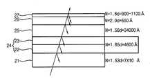
상기 베이스 기판(11)의 굴절율은 1.53이고 두께는 7*106[Å]이고, 상기 하부 절연막(14)의 굴절율은 1.85이고 두께는 5650[Å]이고, 상기 유기 절연막(15)의 굴절율은 1.56이고 두께는 34000[Å]이고, 상기 화소 전극(16)의 굴절율은 2.0이고 두께는 550[Å]이고, 상기 배향막(17)의 굴절율은 1.6이고 두께는 900[Å] 내지 1100[Å]이다.The
상기 제1 어레이 기판(10)에 광을 투과하였을 경우, 투과된 광 중 레드 광의 투과율은 80% 내지 90% 범위에서 크게 변동되는 것을 확인 할 수 있다.When light is transmitted through the first array substrate 10, it may be confirmed that transmittance of red light in the transmitted light varies greatly in a range of 80% to 90%.
한편, 도 5a는 본 발명의 실시예에 따른 제2 어레이 기판의 단면도이다.5A is a cross-sectional view of a second array substrate according to an exemplary embodiment of the present invention.
도 5b는 도 5a의 제2 어레이 기판의 레드 광에 대한 투과율을 나타낸 그래프이다.FIG. 5B is a graph illustrating transmittance of red light of the second array substrate of FIG. 5A.
상기 실시예에 따른 제2 어레이 기판(20)은 베이스 기판(21)위에 하부 절연막(14), 유기 절연막(25), 화소 전극(26) 및 배향막(27)이 순차적으로 형성된다. 상기 하부 절연막(24)은 게이트 절연막(22)과 보호 절연막(23)을 포함한다.In the second array substrate 20 according to the exemplary embodiment, the lower insulating
상기 베이스 기판(21)의 굴절율은 1.53이고 두께는 7*06[Å]이고, 상기 하부 절연막(24)의 굴절율은 1.85이고 두께는 4600[Å]이고, 상기 유기 절연막(25)의 굴절율은 1.56이고 두께는 34000[Å]이고, 상기 화소 전극(26)의 굴절율은 2.0이고 두께는 550[Å]이고, 상기 배향막(27)의 굴절율은 1.6이고 두께는 900[Å] 내지 1100[Å]이다.The
상기 비교예의 제1 어레이 기판(10)과 비교해 볼 때, 상기 실시예에 따른 제 2 어레이 기판(20)의 하부 절연막(24)은 상기 제1 어레이 기판(10)의 하부 절연막(14)의 두께에 비해 상대적으로 얇게 형성된다.Compared with the first array substrate 10 of the comparative example, the lower insulating
상기와 같이 상대적으로 얇게 형성된 하부 절연막(24)을 갖는 상기 제2 어레이 기판(20)에 광을 투과하였을 경우, 투과된 광 중 레드 광의 투과율은 대략 84% 를 유지하면서 거의 변동되지 않는 것을 확인 할 수 있다.When light is transmitted through the second array substrate 20 having the relatively thin lower insulating
이와 같이 제1 어레이 기판(10)과 제2 어레이 기판(20)을 비교해 본 결과, 상기 유기 절연막의 두께 편차에 따른 레드 광의 투과율이 변동폭을 상기 유기 절연막의 하부에 형성된 하부 절연막의 두께를 조정함으로써 상기 레드 광의 투과율 변동폭을 완만하게 할 수 있다.As a result of comparing the first array substrate 10 and the second array substrate 20 as described above, the transmittance of the red light due to the thickness variation of the organic insulating film is adjusted by adjusting the thickness of the lower insulating film formed under the organic insulating film. The variation in transmittance of the red light can be made gentle.
이러한 유기 절연막의 두께 변동에 따른 투과율의 변동폭을 최소화하기 위한 투과되는 광의 레드 피크 파장대(W)에 대한 하부 절연막의 두께(D)는 다음의 수학식 1로 정의된다.The thickness D of the lower insulating film with respect to the red peak wavelength band W of transmitted light for minimizing the variation in transmittance due to the thickness variation of the organic insulating film is defined by

여기서, 상기 파장의 단위는 nm 이고, 상기 두께의 단위는 Å이고, N은 상기 하부절연막의 굴절율이다.Here, the unit of the wavelength is nm, the unit of the thickness is Å, N is the refractive index of the lower insulating film.
도 6 내지 도 9는 도 1에 도시된 어레이 기판의 제조 방법을 설명하기 위한 공정도들이다.6 to 9 are process diagrams for describing a method of manufacturing the array substrate illustrated in FIG. 1.
도 1 및 도 6을 참조하면, 베이스 기판(101) 위에 게이트 금속층을 증착 및 패터닝하여 게이트 금속패턴을 형성한다. 상기 게이트 금속패턴은 게이트 배선GLn), 스토리지 공통 배선(121) 및 게이트 전극(111)을 포함한다.1 and 6, a gate metal pattern is formed by depositing and patterning a gate metal layer on the
상기 게이트 금속패턴이 형성된 베이스 기판(101) 위에 게이트 절연막(102)을 형성한다. 상기 게이트 절연막(102)은 질화 실리콘(SiNx)과 같은 절연 물질로 대략 3200Å 내지 3800Å의 두께로 형성된다.A
도 1 및 도 7을 참조하면, 상기 게이트 절연막(102) 위에 채널층(112)을 형성한다. 구체적으로, 상기 게이트 절연막(102) 위에 아몰퍼스 실리콘막 및 인 시튜(in-situ) 도핑된 n+ 아몰퍼스 실리콘막을 차례로 형성한다. 상기 아몰퍼스 실리콘막(112a) 및 n+ 아몰퍼스 실리콘막(112b)을 패터닝하여 상기 게이트 전극(111)에 대응하여 상기 채널층(112)을 형성한다.1 and 7, the
도 1 및 도 8을 참조하면, 상기 채널층(112) 위에 데이터 금속층을 증착 및 패터닝하여 소스 금속패턴을 형성한다.1 and 8, a source metal pattern is formed by depositing and patterning a data metal layer on the
상기 소스 금속패턴은 상기 소스 배선(DLm), 상기 소스 전극(113), 상기 드레인 전극(114), 상기 스토리지 캐패시터(CST)의 전극 패턴(123)을 포함한다.The source metal pattern includes the source wiring DLm, the
이후, 상기 소스 및 드레인 전극(113, 114)을 마스크로 노출된 상기 채널층(112)의 n+ 아몰퍼스 실리콘막(112b)을 제거하여 상기 스위칭 소자(TFT)의 채널 영역을 정의한다.Thereafter, the n+
상기 소스 금속패턴이 형성된 베이스 기판(101) 위에 보호 절연막(103)을 형성한다. 상기 보호 절연막(103)은 질화 실리콘(SiNx)과 같은 절연 물질로 대략 800 Å 내지 1200Å의 두께로 형성된다.A protective insulating
하부 절연막(104), 즉, 상기 게이트 절연막(102) 및 보호 절연막(103)의 두께는 상기 어레이 기판을 투과하는 광의 레드 광의 피크 파장대에 연동하여 결정된다. 일반적으로 상기 게이트 절연막(102)의 두께는 상기 스위칭 소자(TFT)의 전기적인 특성을 고려하여 최소치가 결정된다. 이에 바람직하게는 상기 보호 절연막(103)의 두께를 상기 레드 광의 피크 파장대에 연동하여 조정한다.The thickness of the lower insulating
따라서, 하부 절연막(104)의 두께(D)를 앞서 설명된 수학식 1에 따라 레드 광의 피크 파장대(W)에 연동된 두께로 형성한다.Therefore, the thickness D of the lower insulating
도 1 및 도 9를 참조하면, 상기 보호 절연막(103)이 형성된 베이스 기판(101) 위에 유기 절연막(105)을 형성한다. 상기 유기 절연막(105)은 상기 유기 절연막(105)은 대략 2㎛ 내지 4.3㎛ 의 두께로 형성된다. 상기 유기 절연막(105)의 굴절율은 약 1.56 이다. 상기 유기 절연막(105)은 상기 베이스 기판(101) 위에 형성되는 다른 층들에 비해 상대적으로 두껍게 형성되는 공정 특성에 따라 균일한 두께로 형성되지 못한다. 이러한 유기 절연막(105)의 두께 편차는 광의 투과율을 변동시킨다.1 and 9, an organic insulating
이에, 상기 광의 레드 피크 파장대(W)에 연동된 두께(D)를 갖는 하부 절연막(104)은 상기 유기 절연막(105)의 두께 편차에 의해 발생된 투과율 변동을 보상한다.Accordingly, the lower insulating
상기 유기 절연막(105) 및 보호 절연막(103)에 콘택홀(117)을 형성하여 상기 드레인 전극(114)의 일부분을 노출시킨다.A
이, 상기 콘택홀(117)이 형성된 베이스 기판(101) 위에 투명 전도성 물질을 증착 및 패터닝하여 화소 전극(PE)을 형성한다. 상기 투명 전도성 물질은 인듐-틴-옥사이드(Indium-Tin-Oxide : ITO), 인듐-아연-옥사이드(Indium-Zinc-Oxide : IZO) 또는 인듐-틴-아연 옥사이드(Indium-Tin-Zinc-Oxide)를 포함한다.The pixel electrode PE is formed by depositing and patterning a transparent conductive material on the
상기 화소 전극(PE)은 상기 소스 배선들(DLm-1, DLm)의 일부분을 커버하도록 형성된다. 이에 의해 상기 화소 전극(PE)의 형성 면적을 최대로 확장함에 따라서 상기 화소 전극(PE)을 투과하는 광의 투과율을 향상시킨다.The pixel electrode PE is formed to cover a portion of the source lines DLm-1 and DLm. As a result, the transmittance of light passing through the pixel electrode PE is improved by maximizing the formation area of the pixel electrode PE.
이상과 같이 상기 유기 절연막(105)의 하부에 형성된 하부 절연막(104)의 두께(D)를 레드 광 피크 파장대(W)에 연동하여 형성함으로써 상기 유기 절연막(105)의 두께 변동에 따른 투과율의 변동을 완만하게 하여 표시 품질을 향상시킨다.As described above, the thickness D of the lower insulating
도 10은 본 발명의 다른 실시예에 따른 액정표시패널의 단면도이다.10 is a cross-sectional view of a liquid crystal display panel according to another exemplary embodiment of the present invention.
도 10을 참조하면, 상기 액정표시패널은 어레이 기판(100), 대향 기판(200) 및 액정층(300)을 포함한다.Referring to FIG. 10, the liquid crystal display panel includes an
상기 어레이 기판(100)은 상기 도 1 및 도 2에서 설명된 바와 실질적으로 동일하므로, 상세한 설명은 생략한다.Since the
상기 어레이 기판(100)의 유기 절연막(105) 아래에 형성된 하부 절연막(104)의 두께(D)는 상기 수학식 1에 나타낸 바와 같이, 상기 어레이 기판(100)의 배면으로부터 제공되는 광의 레드 광 피크 파장대(W)에 연동하여 결정된다.The thickness D of the lower insulating
상기 수학식 1에 따른 두께(D)를 갖는 상기 하부 절연막(104)은 상기 유기 절연막(105)의 두께 편차에 의한 광의 투과율 변동율을 완만하게 보상한다. 이에 의해 화이트 화면 구동시 붉은 얼룩 현상을 개선할 수 있다.The lower
상기 대향 기판(200)은 베이스 기판(201)을 포함한다. 상기 베이스 기판(201)위에는 차광층(210), 컬러필터층(220), 오버 코팅층(230) 및 공통전극층(240)이 형성된다. The opposing
상기 차광층(210)은 게이트 배선들(GLn-1, GLn), 소스 배선들(DLm-1, DLm) 및 스위칭 소자(TFT)에 대응하여 형성되며, 상기 어레이 기판(100) 및 액정층(300)을 투과한 광(L)을 차단한다.The light blocking layer 210 is formed to correspond to the gate lines GLn-1 and GLn, the source lines DLm-1 and DLm, and the switching element TFT, and the
상기 컬러필터층(220)은 상기 어레이 기판(100)의 화소 영역들에 대응하여 형성된 컬러필터패턴들을 포함한다. 상기 컬러필터패턴들은 레드(R), 그린(G) 및 블루(B) 필터패턴을 포함한다.The color filter layer 220 includes color filter patterns formed to correspond to the pixel areas of the
상기 오버 코팅층(230)은 상기 컬러필터층(220) 위에 형성되어, 상기 컬러필터층(220)을 보호하고, 더불어 상기 대향 기판(200)을 평탄화시킨다.The overcoat layer 230 is formed on the color filter layer 220 to protect the color filter layer 220 and to planarize the
상기 공통 전극층(240)은 상기 어레이 기판의 화소 전극(PE)에 대향하는 전극으로, 상기 화소 전극(PE) 및 액정층(300)에 의해 액정 캐패시터가 정의된다.The common electrode layer 240 is an electrode facing the pixel electrode PE of the array substrate, and a liquid crystal capacitor is defined by the pixel electrode PE and the
상기 액정층(300)은 상기 어레이 기판(100)과 상기 대향 기판(200) 사이에 개재되어, 상기 화소 전극(PE)과 상기 공통 전극(240) 간의 전위차에 의해 액정층(300)의 배열각을 변화시켜 영상을 표시한다.The
도 11은 본 발명의 또 다른 실시예에 따른 액정표시장치의 분해 사시도이다.11 is an exploded perspective view of a liquid crystal display according to another exemplary embodiment of the present invention.
도 11을 참조하면, 상기 액정표시장치는 백라이트 어셈블리(400) 및 디스플레이 어셈블리(500)를 포함한다.Referring to FIG. 11, the liquid crystal display includes a
상기 백라이트 어셈블리(400)는 수납 용기(410), 반사판(420), 램프 어셈블리(430), 프레임부(440, 450, 460) 및 광학 부재(470)를 포함한다.The
상기 수납 용기(410)에는 상기 반사판(420), 램프 어셈블리(430)와, 프레임부(440, 450, 460) 및 광학 부재(470)가 수납된다.The reflecting plate 420, the
상기 램프 어셈블리(430)는 램프(431), 램프 와이어(432), 램프 홀더(433) 및 램프 고정부재(434)를 포함한다.The
상기 램프(431)는 내부에 전극이 형성된 내부 전극 형광 램프(CCFL)이다. 상기 램프(431)의 내벽에는 형광층이 도포되고, 내부에는 방전 가스(131b)가 충진된다. 상기 방전 가스는 예를 들면, 수은(mercury), 미량의 아르곤(Argon, Ar), 네온(Neon, Ne), 크세논(Xenon, Xe) 및 크립톤(Krypton, Kr)을 포함한다.The
상기 램프(431)는 내부 전극에 구동전압이 인가되면, 상기 방전 가스를 방전시켜 비가시광선인, 예를 들면, 자외선이 발생되고, 자외선은 램프(431)의 내측벽에 도포된 레드(R), 그린(G) 및 블루(B) 형광층에 의하여 가시광선으로 변경된다.When the driving voltage is applied to the internal electrode, the
상기 레드(R) 형광층에 의해 여기된 레드 광의 피크 파장대(W)에 연동하여 상기 디스플레이 어셈블리의 액정표시패널이 제조된다. 구체적으로 상기 램프(431)에서 발생된 광 중 레드 광의 피크 파장대(W)에 기초하여 상기 수학식 1에 따라서 상기 액정표시패널의 어레이 기판에 형성되는 하부 유기막의 두께(D)가 결정된다.The liquid crystal display panel of the display assembly is manufactured in association with the peak wavelength band W of the red light excited by the red (R) fluorescent layer. Specifically, the thickness D of the lower organic layer formed on the array substrate of the liquid crystal display panel is determined according to
상기 램프 와이어(432)는 상기 램프의 내부 전극과 전기적으로 연결되어 상기 구동전압을 전달한다.The
상기 램프 홀더(433)는 상기 램프(431)의 일단부를 홀딩하고, 상기 램프 와이어(432)를 인출하기 위한 인출홀(미도시)과 상기 램프 홀더(433)를 상기 수납 용기(410)에 고정하기 위한 고정돌기(미도시)가 형성된다.The
상기 램프 고정부재(434)는 상기 램프(431)의 타단부를 고정하며, 상기 램프의 타단부 형상에 대응하는 고정홈(434a)이 형성된다.The
상기 프레임부(440, 450, 460)는 제1 사이드 몰드(440), 제2 사이드 몰드(450) 및 램프 지지부재(460)를 포함한다. 상기 제1 사이드 몰드(440)는 상기 램프 홀더(433)를 커버함으로써 상기 램프(431)의 일단부를 커버하고, 상기 광학 부재(770)를 지지한다. 상기 제2 사이드 몰드(450)는 상기 램프 고정부재(434)를 커버함으로써 상기 램프(431)의 타단부를 커버하고, 상기 광학 부재(470)를 지지한다.The
상기 광학 부재(470)는 확산판(471)과 집광 시트들(472, 473)을 포함한다. 상기 확산판(471)은 상기 램프(431)로부터 출사된 광을 확산시켜 광의 휘도 균일성을 보다 향상시킨다.The optical member 470 includes a
상기 디스플레이 어셈블리(500)는 미들 몰드(510), 액정표시패널(520), 인쇄회로기판(530), 연성회로기판(540) 및 탑 샤시(550)를 포함한다.The
상기 미들 몰드(510)는 광학 부재(470)가 배치된 수납 용기(410) 위에 배치되어 상기 제1 및 제2 사이드 몰드(440, 450)에 위에 안착된 광학 부재(470)의 가장자리를 눌러 상기 수납 용기(410)로부터 상기 광학 부재(470)가 이탈되는 것을 방지한다.The
상기 액정표시패널(520)은 어레이 기판(521)과 상기 어레이 기판(521)에 대 향하는 대향 기판(522) 및 상기 어레이 기판과 대향 기판(521, 522) 사이에 개재된 액정층(미도시)을 포함한다.The liquid
상기 어레이 기판(521)의 유기 절연막 아래에 형성된 하부 절연막의 두께(D)는 상기 수학식 1에 나타낸 바와 같이, 상기 백라이트 어셈블리(400)로부터 발생된 광의 레드 광 피크 파장대(W)에 연동하여 결정된다. 상기 수학식 1에 따른 두께(D)를 갖는 상기 하부 절연막은 상기 유기 절연막의 두께 편차에 의한 광의 투과율 변동율을 완만하게 보상한다. 이에 의해 화이트 화면 구동시 붉은 얼룩 현상을 개선할 수 있다.The thickness D of the lower insulating film formed under the organic insulating film of the
상기 액정표시패널(520)은 도 10에 설명된 액정표시패널과 실질적으로 동일하므로 상세한 설명은 생략한다.Since the liquid
상기 인쇄회로기판(530)은 영상신호를 처리하는 구동회로 유닛(미도시)을 포함하고, 구동회로 유닛은 외부에서 입력된 영상신호 및 제어신호를 신호처리하여 상기 액정표시패널(520)을 구동시키기 위한 구동 제어신호 및 영상신호를 제공한다.The printed
상기 연성회로기판(540)은 상기 액정표시패널(520)과 인쇄회로기판(530)을 전기적으로 연결하여 상기 인쇄회로기판(530)에서 제공된 구동 제어신호 및 영상신호를 이용하여 상기 액정표시패널(520)에 구동신호를 출력한다.The
상기 탑 샤시(550)는 상기 액정표시패널(520)의 가장자리를 감싸고 수납 용기(410)와 결합된다. 상기 탑 샤시(550)는 외부에서 충격으로부터 파손 또는 손상되는 것을 방지하고, 상기 액정표시패널(520)이 상기 수납 용기(410)로부터 이탈되 는 것을 방지한다.The
도 12는 본 발명의 실시예에 따라 표시 품질의 개선 효과를 설명하기 위한 그래프이다.12 is a graph for explaining an effect of improving display quality according to an embodiment of the present invention.
도 12에 도시된 그래프는 상기 액정표시패널에 레드 피크 파장대(W)이 614 nm 인 광이 입사되고 상기 액정표시패널에 화이트로 구동되는 경우, 상기 액정표시패널의 하부 절연막의 두께에 따라서 상기 액정표시패널에 붉은색 얼룩이 발생한 부분과 흰색 얼룩이 발생한 부분 간의 색좌표차(Wx, Wy)를 나타낸 것이다.The graph shown in FIG. 12 shows that when the light having a red peak wavelength (W) of 614 nm is incident on the liquid crystal display panel and is driven to white in the liquid crystal display panel, the liquid crystal according to the thickness of the lower insulating film of the liquid crystal display panel. The difference in color coordinates (Wx, Wy) between a red spot and a white spot in the display panel is shown.
구체적으로, 상기 액정표시패널의 하부 절연막의 두께(D)가 5600Å인 경우, 상기 색좌표차의 X 좌표(Wx)는 대략 0.003 내지 0.006 범위에 존재한다. 반면, 하부 절연막의 두께(D)가 4600Å으로 얇아진 경우, 상기 색좌표차의 X 좌표(Wx)는 대략 0.003 이하 범위에 존재한다. 상기 색좌표차의 X 좌표(Wx)가 '0'에 근접할수록 화이트 균일성이 우수하고, '0'에 원접할수록 화이트 균일성이 저하된다.Specifically, when the thickness D of the lower insulating film of the liquid crystal display panel is 5600Å, the X coordinate Wx of the color coordinate difference is in a range of about 0.003 to 0.006. On the other hand, when the thickness D of the lower insulating film is thinned to 4600 kV, the X coordinate Wx of the color coordinate difference is in a range of about 0.003 or less. The closer the X coordinate Wx of the color coordinate difference is to '0', the better the white uniformity is. The closer to 0, the lower the white uniformity.
즉, 상기 하부 절연막의 두께(D)가 상기 수학식 1 및 표 1에 정의된 바와 같이, 레드 광의 피크 파장대(W)이 614nm 인 경우 4600Å 두께의 하부 절연막을 갖는 액정표시패널은 상기 색좌표차(Wx, Wy)는 0.003 이하가 된다. 결과적으로 상기 레드 광의 피크 파장대에 연동되어 조정된 두께의 하부 절연막을 갖는 액정표시패널은 얼룩 불량이 개선되었음을 알 수 있다.That is, when the thickness D of the lower insulating film is defined in
이상에서 설명한 바와 같이, 본 발명에 따르면 레드 피크 파장대에 연동된 두께로 하부 절연막을 형성함으로써 상기 액정표시패널의 유기 절연막의 두께 편차 에 따른 광의 투과율 변동을 완화시킬 수 있다.As described above, according to the present invention, by forming the lower insulating film having a thickness interlocked with the red peak wavelength band, it is possible to mitigate the variation in the transmittance of light due to the thickness variation of the organic insulating film of the liquid crystal display panel.
따라서, 상기 액정표시패널의 광 투과율 변동을 완화시킴으로써 상기 액정표시패널에 표시되는 영상의 표시 품질을 향상시킬 수 있다.Therefore, the display quality of the image displayed on the liquid crystal display panel can be improved by alleviating the variation in the light transmittance of the liquid crystal display panel.
이상에서는 실시예를 참조하여 설명하였지만, 해당 기술 분야의 숙련된 당업자는 하기의 특허 청구의 범위에 기재된 본 발명의 사상 및 영역으로부터 벗어나지 않는 범위 내에서 본 발명을 다양하게 수정 및 변경시킬 수 있음을 이해할 수 있을 것이다.Although described above with reference to the embodiments, those skilled in the art can be variously modified and changed within the scope of the invention without departing from the spirit and scope of the invention described in the claims below. I can understand.
Claims (30)
Translated fromKorean


Priority Applications (5)
| Application Number | Priority Date | Filing Date | Title |
|---|---|---|---|
| KR1020050087031AKR101189152B1 (en) | 2005-09-16 | 2005-09-16 | Array substrate, liquid display panel and liquid crystal display having the same |
| US11/516,227US7675590B2 (en) | 2005-09-16 | 2006-09-06 | Array substrate, liquid crystal display panel and liquid crystal display device having the same |
| CN2006101538375ACN1933165B (en) | 2005-09-16 | 2006-09-13 | Array substrate, liquid crystal display panel and liquid crystal display device having the same |
| JP2006251812AJP5068499B2 (en) | 2005-09-16 | 2006-09-15 | Array substrate, liquid crystal display panel having the same, and liquid crystal display device |
| TW095134220ATWI409954B (en) | 2005-09-16 | 2006-09-15 | Array substrate, liquid crystal display panel and liquid crystal display device having the same |
Applications Claiming Priority (1)
| Application Number | Priority Date | Filing Date | Title |
|---|---|---|---|
| KR1020050087031AKR101189152B1 (en) | 2005-09-16 | 2005-09-16 | Array substrate, liquid display panel and liquid crystal display having the same |
Publications (2)
| Publication Number | Publication Date |
|---|---|
| KR20070032119A KR20070032119A (en) | 2007-03-21 |
| KR101189152B1true KR101189152B1 (en) | 2012-10-10 |
Family
ID=37878887
Family Applications (1)
| Application Number | Title | Priority Date | Filing Date |
|---|---|---|---|
| KR1020050087031AExpired - LifetimeKR101189152B1 (en) | 2005-09-16 | 2005-09-16 | Array substrate, liquid display panel and liquid crystal display having the same |
Country Status (5)
| Country | Link |
|---|---|
| US (1) | US7675590B2 (en) |
| JP (1) | JP5068499B2 (en) |
| KR (1) | KR101189152B1 (en) |
| CN (1) | CN1933165B (en) |
| TW (1) | TWI409954B (en) |
Families Citing this family (7)
| Publication number | Priority date | Publication date | Assignee | Title |
|---|---|---|---|---|
| JP6069362B2 (en)* | 2012-12-28 | 2017-02-01 | シャープ株式会社 | LCD display |
| KR20150028608A (en)* | 2013-09-06 | 2015-03-16 | 삼성디스플레이 주식회사 | Display panel |
| US9530801B2 (en)* | 2014-01-13 | 2016-12-27 | Apple Inc. | Display circuitry with improved transmittance and reduced coupling capacitance |
| KR102563157B1 (en)* | 2015-08-26 | 2023-08-04 | 엘지디스플레이 주식회사 | Thin film transistor and display device |
| CN205787504U (en)* | 2016-05-31 | 2016-12-07 | 京东方科技集团股份有限公司 | A kind of array base palte and display device |
| KR102812392B1 (en)* | 2019-03-28 | 2025-05-26 | 삼성디스플레이 주식회사 | Display panel and device including the same |
| CN114690464A (en)* | 2022-03-21 | 2022-07-01 | Tcl华星光电技术有限公司 | Display panel and manufacturing method thereof |
Family Cites Families (8)
| Publication number | Priority date | Publication date | Assignee | Title |
|---|---|---|---|---|
| JP3191085B2 (en)* | 1996-01-29 | 2001-07-23 | 株式会社日立製作所 | Reflective liquid crystal display element and liquid crystal display device |
| KR100226494B1 (en)* | 1997-02-20 | 1999-10-15 | 김영환 | LCD and its manufacturing method |
| JP2003051599A (en)* | 2001-05-24 | 2003-02-21 | Semiconductor Energy Lab Co Ltd | Semiconductor devices and electronic equipment |
| KR100759978B1 (en) | 2001-07-12 | 2007-09-18 | 삼성전자주식회사 | Vertically oriented liquid crystal display device and color filter substrate used therein |
| KR100820647B1 (en) | 2001-10-29 | 2008-04-08 | 엘지.필립스 엘시디 주식회사 | Array board for transflective liquid crystal display device and manufacturing method thereof |
| KR100959683B1 (en) | 2001-12-28 | 2010-05-26 | 엘지디스플레이 주식회사 | Reflective Liquid Crystal Display and Manufacturing Method Thereof |
| JP4417072B2 (en)* | 2003-03-28 | 2010-02-17 | シャープ株式会社 | Substrate for liquid crystal display device and liquid crystal display device using the same |
| JP4624078B2 (en)* | 2003-11-14 | 2011-02-02 | 株式会社半導体エネルギー研究所 | Method for manufacturing liquid crystal display device |
- 2005
- 2005-09-16KRKR1020050087031Apatent/KR101189152B1/ennot_activeExpired - Lifetime
- 2006
- 2006-09-06USUS11/516,227patent/US7675590B2/enactiveActive
- 2006-09-13CNCN2006101538375Apatent/CN1933165B/enactiveActive
- 2006-09-15TWTW095134220Apatent/TWI409954B/enactive
- 2006-09-15JPJP2006251812Apatent/JP5068499B2/enactiveActive
Also Published As
| Publication number | Publication date |
|---|---|
| CN1933165A (en) | 2007-03-21 |
| KR20070032119A (en) | 2007-03-21 |
| JP2007086782A (en) | 2007-04-05 |
| US7675590B2 (en) | 2010-03-09 |
| CN1933165B (en) | 2010-12-22 |
| JP5068499B2 (en) | 2012-11-07 |
| TWI409954B (en) | 2013-09-21 |
| TW200721502A (en) | 2007-06-01 |
| US20070064166A1 (en) | 2007-03-22 |
Similar Documents
| Publication | Publication Date | Title |
|---|---|---|
| JP5313373B2 (en) | Liquid crystal display | |
| JP4167085B2 (en) | Liquid crystal display | |
| KR100787914B1 (en) | Transflective type liquid crystal apparatus and method for manufacturing thin film transistor board thereof | |
| JP4490948B2 (en) | Liquid crystal display element, color filter substrate and manufacturing method thereof | |
| US7206042B2 (en) | Color filter substrate and liquid crystal display apparatus having the same | |
| US7973888B2 (en) | Liquid crystal display device having minimized outer region | |
| KR100831091B1 (en) | Transflective liquid crystal display, flat panel display device, and electronic apparatus | |
| US20130300990A1 (en) | Image display device | |
| JP5068499B2 (en) | Array substrate, liquid crystal display panel having the same, and liquid crystal display device | |
| US7342626B2 (en) | Display device | |
| JP2006313358A (en) | Liquid crystal display | |
| US7656482B2 (en) | Transflective liquid crystal display and panel therefor | |
| KR20080026721A (en) | Color filter substrate and liquid crystal display device having the same | |
| CN111158199B (en) | An array substrate and display device | |
| KR100995581B1 (en) | Color filter substrate, liquid crystal display device having same and manufacturing method thereof | |
| US20050124087A1 (en) | Method for manufacturing electro-optical device, electro-optical device, and electronic equipment | |
| KR101020659B1 (en) | Reflective type liquid crystal display device | |
| KR100487434B1 (en) | Liquid Crystal Display Device and Method for Manufacturing the Same | |
| KR20020041606A (en) | Liquid crystal display device and method for manufacturing the same | |
| KR20080050830A (en) | LCD Display | |
| KR20070043473A (en) | Reflective-transmissive display substrate and liquid crystal display panel having same | |
| KR20060078072A (en) | LCD Display | |
| KR20040105435A (en) | Array substrate for enhancing display quality, method for manufacturing the same and liquid crystal display device having the same | |
| JP2008242152A (en) | Manufacturing method of liquid crystal display panel, liquid crystal display panel, and electronic device | |
| KR20070082636A (en) | Display panel |
Legal Events
| Date | Code | Title | Description |
|---|---|---|---|
| PA0109 | Patent application | Patent event code:PA01091R01D Comment text:Patent Application Patent event date:20050916 | |
| PG1501 | Laying open of application | ||
| A201 | Request for examination | ||
| PA0201 | Request for examination | Patent event code:PA02012R01D Patent event date:20100816 Comment text:Request for Examination of Application Patent event code:PA02011R01I Patent event date:20050916 Comment text:Patent Application | |
| E902 | Notification of reason for refusal | ||
| PE0902 | Notice of grounds for rejection | Comment text:Notification of reason for refusal Patent event date:20111219 Patent event code:PE09021S01D | |
| E701 | Decision to grant or registration of patent right | ||
| PE0701 | Decision of registration | Patent event code:PE07011S01D Comment text:Decision to Grant Registration Patent event date:20120703 | |
| N231 | Notification of change of applicant | ||
| PN2301 | Change of applicant | Patent event date:20120913 Comment text:Notification of Change of Applicant Patent event code:PN23011R01D | |
| GRNT | Written decision to grant | ||
| PR0701 | Registration of establishment | Comment text:Registration of Establishment Patent event date:20121002 Patent event code:PR07011E01D | |
| PR1002 | Payment of registration fee | Payment date:20121004 End annual number:3 Start annual number:1 | |
| PG1601 | Publication of registration | ||
| FPAY | Annual fee payment | Payment date:20150930 Year of fee payment:4 | |
| PR1001 | Payment of annual fee | Payment date:20150930 Start annual number:4 End annual number:4 | |
| FPAY | Annual fee payment | Payment date:20170928 Year of fee payment:6 | |
| PR1001 | Payment of annual fee | Payment date:20170928 Start annual number:6 End annual number:6 | |
| FPAY | Annual fee payment | Payment date:20181001 Year of fee payment:7 | |
| PR1001 | Payment of annual fee | Payment date:20181001 Start annual number:7 End annual number:7 | |
| PR1001 | Payment of annual fee | Payment date:20201005 Start annual number:9 End annual number:9 | |
| PR1001 | Payment of annual fee | Payment date:20210927 Start annual number:10 End annual number:10 | |
| PR1001 | Payment of annual fee | Payment date:20230925 Start annual number:12 End annual number:12 | |
| PR1001 | Payment of annual fee | Payment date:20240925 Start annual number:13 End annual number:13 |