KR101182442B1 - OLED display apparatus and Method thereof - Google Patents
OLED display apparatus and Method thereofDownload PDFInfo
- Publication number
- KR101182442B1 KR101182442B1KR1020100007444AKR20100007444AKR101182442B1KR 101182442 B1KR101182442 B1KR 101182442B1KR 1020100007444 AKR1020100007444 AKR 1020100007444AKR 20100007444 AKR20100007444 AKR 20100007444AKR 101182442 B1KR101182442 B1KR 101182442B1
- Authority
- KR
- South Korea
- Prior art keywords
- light emitting
- layer
- emitting layer
- red
- green
- Prior art date
- Legal status (The legal status is an assumption and is not a legal conclusion. Google has not performed a legal analysis and makes no representation as to the accuracy of the status listed.)
- Active
Links
- 238000000034methodMethods0.000titleclaimsabstractdescription43
- 238000004519manufacturing processMethods0.000claimsabstractdescription15
- 238000000059patterningMethods0.000claimsabstractdescription13
- 230000005525hole transportEffects0.000claimsdescription34
- 238000002347injectionMethods0.000claimsdescription33
- 239000007924injectionSubstances0.000claimsdescription33
- 239000000758substrateSubstances0.000claimsdescription31
- 239000000463materialSubstances0.000claimsdescription30
- 229910052751metalInorganic materials0.000claimsdescription11
- 239000002184metalSubstances0.000claimsdescription11
- 230000008569processEffects0.000abstractdescription7
- 230000000694effectsEffects0.000abstractdescription2
- 239000010410layerSubstances0.000description200
- 239000002019doping agentSubstances0.000description10
- 229910001111Fine metalInorganic materials0.000description8
- 239000010409thin filmSubstances0.000description6
- 230000000903blocking effectEffects0.000description5
- 229910052782aluminiumInorganic materials0.000description4
- 150000001875compoundsChemical class0.000description4
- 238000000151depositionMethods0.000description4
- 238000010586diagramMethods0.000description4
- 229910052779NeodymiumInorganic materials0.000description3
- 229910052791calciumInorganic materials0.000description3
- 238000006243chemical reactionMethods0.000description3
- 229910052804chromiumInorganic materials0.000description3
- 230000000052comparative effectEffects0.000description3
- 229910052737goldInorganic materials0.000description3
- 229910052741iridiumInorganic materials0.000description3
- 229910052744lithiumInorganic materials0.000description3
- 229910052749magnesiumInorganic materials0.000description3
- IBHBKWKFFTZAHE-UHFFFAOYSA-Nn-[4-[4-(n-naphthalen-1-ylanilino)phenyl]phenyl]-n-phenylnaphthalen-1-amineChemical groupC1=CC=CC=C1N(C=1C2=CC=CC=C2C=CC=1)C1=CC=C(C=2C=CC(=CC=2)N(C=2C=CC=CC=2)C=2C3=CC=CC=C3C=CC=2)C=C1IBHBKWKFFTZAHE-UHFFFAOYSA-N0.000description3
- 229910052759nickelInorganic materials0.000description3
- 239000012044organic layerSubstances0.000description3
- 229910052763palladiumInorganic materials0.000description3
- 229910052697platinumInorganic materials0.000description3
- 229920003227poly(N-vinyl carbazole)Polymers0.000description3
- 229910052709silverInorganic materials0.000description3
- VFUDMQLBKNMONU-UHFFFAOYSA-N9-[4-(4-carbazol-9-ylphenyl)phenyl]carbazoleChemical compoundC12=CC=CC=C2C2=CC=CC=C2N1C1=CC=C(C=2C=CC(=CC=2)N2C3=CC=CC=C3C3=CC=CC=C32)C=C1VFUDMQLBKNMONU-UHFFFAOYSA-N0.000description2
- FAPWRFPIFSIZLT-UHFFFAOYSA-MSodium chlorideChemical compound[Na+].[Cl-]FAPWRFPIFSIZLT-UHFFFAOYSA-M0.000description2
- 239000003990capacitorSubstances0.000description2
- 230000015556catabolic processEffects0.000description2
- 230000008859changeEffects0.000description2
- 238000006731degradation reactionMethods0.000description2
- 239000010408filmSubstances0.000description2
- 239000011521glassSubstances0.000description2
- PJXISJQVUVHSOJ-UHFFFAOYSA-Nindium(III) oxideInorganic materials[O-2].[O-2].[O-2].[In+3].[In+3]PJXISJQVUVHSOJ-UHFFFAOYSA-N0.000description2
- 229910010272inorganic materialInorganic materials0.000description2
- 239000011147inorganic materialSubstances0.000description2
- 238000010791quenchingMethods0.000description2
- 230000000171quenching effectEffects0.000description2
- GEQBRULPNIVQPP-UHFFFAOYSA-N2-[3,5-bis(1-phenylbenzimidazol-2-yl)phenyl]-1-phenylbenzimidazoleChemical compoundC1=CC=CC=C1N1C2=CC=CC=C2N=C1C1=CC(C=2N(C3=CC=CC=C3N=2)C=2C=CC=CC=2)=CC(C=2N(C3=CC=CC=C3N=2)C=2C=CC=CC=2)=C1GEQBRULPNIVQPP-UHFFFAOYSA-N0.000description1
- OGGKVJMNFFSDEV-UHFFFAOYSA-N3-methyl-n-[4-[4-(n-(3-methylphenyl)anilino)phenyl]phenyl]-n-phenylanilineChemical compoundCC1=CC=CC(N(C=2C=CC=CC=2)C=2C=CC(=CC=2)C=2C=CC(=CC=2)N(C=2C=CC=CC=2)C=2C=C(C)C=CC=2)=C1OGGKVJMNFFSDEV-UHFFFAOYSA-N0.000description1
- AWXGSYPUMWKTBR-UHFFFAOYSA-N4-carbazol-9-yl-n,n-bis(4-carbazol-9-ylphenyl)anilineChemical compoundC12=CC=CC=C2C2=CC=CC=C2N1C1=CC=C(N(C=2C=CC(=CC=2)N2C3=CC=CC=C3C3=CC=CC=C32)C=2C=CC(=CC=2)N2C3=CC=CC=C3C3=CC=CC=C32)C=C1AWXGSYPUMWKTBR-UHFFFAOYSA-N0.000description1
- DIVZFUBWFAOMCW-UHFFFAOYSA-N4-n-(3-methylphenyl)-1-n,1-n-bis[4-(n-(3-methylphenyl)anilino)phenyl]-4-n-phenylbenzene-1,4-diamineChemical compoundCC1=CC=CC(N(C=2C=CC=CC=2)C=2C=CC(=CC=2)N(C=2C=CC(=CC=2)N(C=2C=CC=CC=2)C=2C=C(C)C=CC=2)C=2C=CC(=CC=2)N(C=2C=CC=CC=2)C=2C=C(C)C=CC=2)=C1DIVZFUBWFAOMCW-UHFFFAOYSA-N0.000description1
- VIJYEGDOKCKUOL-UHFFFAOYSA-N9-phenylcarbazoleChemical compoundC1=CC=CC=C1N1C2=CC=CC=C2C2=CC=CC=C21VIJYEGDOKCKUOL-UHFFFAOYSA-N0.000description1
- OKTJSMMVPCPJKN-UHFFFAOYSA-NCarbonChemical compound[C]OKTJSMMVPCPJKN-UHFFFAOYSA-N0.000description1
- 241000284156Clerodendrum quadriloculareSpecies0.000description1
- 108010043121Green Fluorescent ProteinsProteins0.000description1
- 101000837344Homo sapiens T-cell leukemia translocation-altered gene proteinProteins0.000description1
- 229910018068Li 2 OInorganic materials0.000description1
- 239000004952PolyamideSubstances0.000description1
- 239000004642PolyimideSubstances0.000description1
- 241000083879Polyommatus icarusSpecies0.000description1
- 229910052581Si3N4Inorganic materials0.000description1
- 229910004205SiNXInorganic materials0.000description1
- 229910004298SiO 2Inorganic materials0.000description1
- VYPSYNLAJGMNEJ-UHFFFAOYSA-NSilicium dioxideChemical compoundO=[Si]=OVYPSYNLAJGMNEJ-UHFFFAOYSA-N0.000description1
- XUIMIQQOPSSXEZ-UHFFFAOYSA-NSiliconChemical compound[Si]XUIMIQQOPSSXEZ-UHFFFAOYSA-N0.000description1
- 102100028692T-cell leukemia translocation-altered gene proteinHuman genes0.000description1
- 239000007983Tris bufferSubstances0.000description1
- -1acrylChemical group0.000description1
- XAGFODPZIPBFFR-UHFFFAOYSA-NaluminiumChemical compound[Al]XAGFODPZIPBFFR-UHFFFAOYSA-N0.000description1
- 150000001412aminesChemical class0.000description1
- 229940027991antiseptic and disinfectant quinoline derivativeDrugs0.000description1
- QVQLCTNNEUAWMS-UHFFFAOYSA-Nbarium oxideInorganic materials[Ba]=OQVQLCTNNEUAWMS-UHFFFAOYSA-N0.000description1
- 230000008901benefitEffects0.000description1
- 230000005540biological transmissionEffects0.000description1
- 230000015572biosynthetic processEffects0.000description1
- XJHCXCQVJFPJIK-UHFFFAOYSA-Mcaesium fluorideInorganic materials[F-].[Cs+]XJHCXCQVJFPJIK-UHFFFAOYSA-M0.000description1
- 150000001716carbazolesChemical class0.000description1
- 239000011248coating agentSubstances0.000description1
- 238000000576coating methodMethods0.000description1
- 239000002131composite materialSubstances0.000description1
- 239000004020conductorSubstances0.000description1
- XCJYREBRNVKWGJ-UHFFFAOYSA-Ncopper(II) phthalocyanineChemical compound[Cu+2].C12=CC=CC=C2C(N=C2[N-]C(C3=CC=CC=C32)=N2)=NC1=NC([C]1C=CC=CC1=1)=NC=1N=C1[C]3C=CC=CC3=C2[N-]1XCJYREBRNVKWGJ-UHFFFAOYSA-N0.000description1
- 239000006059cover glassSubstances0.000description1
- 230000002950deficientEffects0.000description1
- 230000008021depositionEffects0.000description1
- 238000005538encapsulationMethods0.000description1
- 239000011888foilSubstances0.000description1
- 238000004680force modulation microscopyMethods0.000description1
- 229910021389grapheneInorganic materials0.000description1
- RBTKNAXYKSUFRK-UHFFFAOYSA-Nheliogen blueChemical compound[Cu].[N-]1C2=C(C=CC=C3)C3=C1N=C([N-]1)C3=CC=CC=C3C1=NC([N-]1)=C(C=CC=C3)C3=C1N=C([N-]1)C3=CC=CC=C3C1=N2RBTKNAXYKSUFRK-UHFFFAOYSA-N0.000description1
- 239000011810insulating materialSubstances0.000description1
- PQXKHYXIUOZZFA-UHFFFAOYSA-Mlithium fluorideInorganic materials[Li+].[F-]PQXKHYXIUOZZFA-UHFFFAOYSA-M0.000description1
- 239000011159matrix materialSubstances0.000description1
- 230000007246mechanismEffects0.000description1
- 238000012986modificationMethods0.000description1
- 230000004048modificationEffects0.000description1
- 150000002894organic compoundsChemical class0.000description1
- 239000011368organic materialSubstances0.000description1
- 239000005416organic matterSubstances0.000description1
- 229920003023plasticPolymers0.000description1
- 239000004033plasticSubstances0.000description1
- 229920002647polyamidePolymers0.000description1
- 229920001721polyimidePolymers0.000description1
- 150000003248quinolinesChemical class0.000description1
- 230000006798recombinationEffects0.000description1
- 238000005215recombinationMethods0.000description1
- 229910052710siliconInorganic materials0.000description1
- 239000010703siliconSubstances0.000description1
- HQVNEWCFYHHQES-UHFFFAOYSA-Nsilicon nitrideChemical compoundN12[Si]34N5[Si]62N3[Si]51N64HQVNEWCFYHHQES-UHFFFAOYSA-N0.000description1
- 229910052814silicon oxideInorganic materials0.000description1
- 239000011780sodium chlorideSubstances0.000description1
- 238000004544sputter depositionMethods0.000description1
- TVIVIEFSHFOWTE-UHFFFAOYSA-Ktri(quinolin-8-yloxy)alumaneChemical compound[Al+3].C1=CN=C2C([O-])=CC=CC2=C1.C1=CN=C2C([O-])=CC=CC2=C1.C1=CN=C2C([O-])=CC=CC2=C1TVIVIEFSHFOWTE-UHFFFAOYSA-K0.000description1
- 238000001771vacuum depositionMethods0.000description1
- XLYOFNOQVPJJNP-UHFFFAOYSA-NwaterSubstancesOXLYOFNOQVPJJNP-UHFFFAOYSA-N0.000description1
Images


Classifications
- H—ELECTRICITY
- H10—SEMICONDUCTOR DEVICES; ELECTRIC SOLID-STATE DEVICES NOT OTHERWISE PROVIDED FOR
- H10K—ORGANIC ELECTRIC SOLID-STATE DEVICES
- H10K59/00—Integrated devices, or assemblies of multiple devices, comprising at least one organic light-emitting element covered by group H10K50/00
- H10K59/30—Devices specially adapted for multicolour light emission
- H10K59/35—Devices specially adapted for multicolour light emission comprising red-green-blue [RGB] subpixels
- H—ELECTRICITY
- H10—SEMICONDUCTOR DEVICES; ELECTRIC SOLID-STATE DEVICES NOT OTHERWISE PROVIDED FOR
- H10K—ORGANIC ELECTRIC SOLID-STATE DEVICES
- H10K50/00—Organic light-emitting devices
- H10K50/10—OLEDs or polymer light-emitting diodes [PLED]
- H10K50/11—OLEDs or polymer light-emitting diodes [PLED] characterised by the electroluminescent [EL] layers
- H10K50/125—OLEDs or polymer light-emitting diodes [PLED] characterised by the electroluminescent [EL] layers specially adapted for multicolour light emission, e.g. for emitting white light
- H10K50/13—OLEDs or polymer light-emitting diodes [PLED] characterised by the electroluminescent [EL] layers specially adapted for multicolour light emission, e.g. for emitting white light comprising stacked EL layers within one EL unit
- H—ELECTRICITY
- H10—SEMICONDUCTOR DEVICES; ELECTRIC SOLID-STATE DEVICES NOT OTHERWISE PROVIDED FOR
- H10K—ORGANIC ELECTRIC SOLID-STATE DEVICES
- H10K50/00—Organic light-emitting devices
- H10K50/10—OLEDs or polymer light-emitting diodes [PLED]
- H10K50/14—Carrier transporting layers
- H—ELECTRICITY
- H10—SEMICONDUCTOR DEVICES; ELECTRIC SOLID-STATE DEVICES NOT OTHERWISE PROVIDED FOR
- H10K—ORGANIC ELECTRIC SOLID-STATE DEVICES
- H10K50/00—Organic light-emitting devices
- H10K50/80—Constructional details
- H10K50/85—Arrangements for extracting light from the devices
- H10K50/852—Arrangements for extracting light from the devices comprising a resonant cavity structure, e.g. Bragg reflector pair
- H—ELECTRICITY
- H10—SEMICONDUCTOR DEVICES; ELECTRIC SOLID-STATE DEVICES NOT OTHERWISE PROVIDED FOR
- H10K—ORGANIC ELECTRIC SOLID-STATE DEVICES
- H10K59/00—Integrated devices, or assemblies of multiple devices, comprising at least one organic light-emitting element covered by group H10K50/00
- H10K59/30—Devices specially adapted for multicolour light emission
- H10K59/35—Devices specially adapted for multicolour light emission comprising red-green-blue [RGB] subpixels
- H10K59/352—Devices specially adapted for multicolour light emission comprising red-green-blue [RGB] subpixels the areas of the RGB subpixels being different
- H—ELECTRICITY
- H10—SEMICONDUCTOR DEVICES; ELECTRIC SOLID-STATE DEVICES NOT OTHERWISE PROVIDED FOR
- H10K—ORGANIC ELECTRIC SOLID-STATE DEVICES
- H10K59/00—Integrated devices, or assemblies of multiple devices, comprising at least one organic light-emitting element covered by group H10K50/00
- H10K59/30—Devices specially adapted for multicolour light emission
- H10K59/35—Devices specially adapted for multicolour light emission comprising red-green-blue [RGB] subpixels
- H10K59/353—Devices specially adapted for multicolour light emission comprising red-green-blue [RGB] subpixels characterised by the geometrical arrangement of the RGB subpixels
- H—ELECTRICITY
- H10—SEMICONDUCTOR DEVICES; ELECTRIC SOLID-STATE DEVICES NOT OTHERWISE PROVIDED FOR
- H10K—ORGANIC ELECTRIC SOLID-STATE DEVICES
- H10K2102/00—Constructional details relating to the organic devices covered by this subclass
- H10K2102/301—Details of OLEDs
- H10K2102/351—Thickness
- H—ELECTRICITY
- H10—SEMICONDUCTOR DEVICES; ELECTRIC SOLID-STATE DEVICES NOT OTHERWISE PROVIDED FOR
- H10K—ORGANIC ELECTRIC SOLID-STATE DEVICES
- H10K59/00—Integrated devices, or assemblies of multiple devices, comprising at least one organic light-emitting element covered by group H10K50/00
- H10K59/80—Constructional details
- H10K59/875—Arrangements for extracting light from the devices
- H10K59/876—Arrangements for extracting light from the devices comprising a resonant cavity structure, e.g. Bragg reflector pair
- H—ELECTRICITY
- H10—SEMICONDUCTOR DEVICES; ELECTRIC SOLID-STATE DEVICES NOT OTHERWISE PROVIDED FOR
- H10K—ORGANIC ELECTRIC SOLID-STATE DEVICES
- H10K71/00—Manufacture or treatment specially adapted for the organic devices covered by this subclass
Landscapes
- Physics & Mathematics (AREA)
- Optics & Photonics (AREA)
- Electroluminescent Light Sources (AREA)
- Devices For Indicating Variable Information By Combining Individual Elements (AREA)
Abstract
Translated fromKoreanDescription
Translated fromKorean본 발명은 유기 발광 디스플레이 장치 및 그의 제조 방법에 관한 것으로, 보다 상세하게는, FMM(Fine Metal Mask)의 교환 횟수를 줄이면서, 수명 및 발광효율이 우수한 유기 발광 디스플레이 장치 및 그의 제조 방법에 관한 것이다.The present invention relates to an organic light emitting display device and a method of manufacturing the same, and more particularly, to an organic light emitting display device and a method of manufacturing the same excellent in lifespan and luminous efficiency while reducing the number of replacement of the FMM (Fine Metal Mask) .
일반적으로, 유기 발광 소자(OLED: Organic Light Emitting Device)는 애노드 전극과 캐소드 전극 사이에 기능성 박막 형태의 유기 발광층이 삽입되어 있는 구조로, 양극에서 정공이 주입되고 음극에서 전자가 주입되어 유기 발광층 내에서 전자와 정공이 결합하여 엑시톤(exciton)이 형성되고 이 엑시톤이 발광 재결합하면서 빛을 내는 소자이다.In general, an organic light emitting device (OLED) is a structure in which an organic light emitting layer in the form of a functional thin film is inserted between an anode electrode and a cathode electrode, and holes are injected from an anode and electrons are injected from an anode, thereby forming an organic light emitting device in the organic light emitting layer. In the electron and hole is combined to form an exciton (exciton) and the exciton is a device that emits light by recombination of light emission.
풀컬러(Full Color) 유기 발광 디스플레이를 구현하는 방법으로는 독립 발광 방식, 컬러 필터(Color Filter) 방식, 색변환 방식 등이 있다. 독립 발광 방식은 R, G, B 각각의 발광 재료를 정교하게 패턴이 되어있는 메탈 새도우 마스크를 사용하여 열증착을 함으로써 R, G, B를 구현하는 방식이다. 컬러 필터 방식은 백색 발광층을 형성하고 R, G, B 컬러 필터를 패터닝하여 R, G, B를 구현하는 방식이다. 색변환 방식은 청색 발광층을 형성하고 청색을 녹색과 적색으로 변화하는 색변환층을 사용하여 R, G, B를 구현하는 방식이다.Methods of implementing a full color organic light emitting display include an independent light emission method, a color filter method, and a color conversion method. The independent light emission method is a method of implementing R, G, and B by thermally depositing each of the R, G, and B light emitting materials using a metal shadow mask with a fine pattern. The color filter method is a method of forming R, G, and B by forming a white light emitting layer and patterning R, G, and B color filters. The color conversion method implements R, RG, and B by forming a blue light emitting layer and using a color conversion layer that changes blue to green and red.
컬러 필터 방식을 이용하는 유기 발광 소자에서는 발광된 백색 발광이 컬러 필터를 거치면서 효율이 감소하기 때문에, 고효율의 백색 발광 재료가 필요하고, 아직까지 메탈 새도우 마스크를 이용한 미세 패터닝 방식에 비하여 전체적인 효율은 낮은 상태이다.In the organic light emitting device using the color filter method, since the emitted white light is reduced in efficiency through the color filter, a high efficiency white light emitting material is required, and the overall efficiency is still lower than that of the fine patterning method using the metal shadow mask. It is a state.
Fine 메탈 새도우 마스크를 이용하여 R, G, B 재료를 증착, 패터닝하는 독립발광방식은 고해상도 및 디스플레이의 사이즈가 커지게 되면 Fine 메탈 새도우 마스크 제작 등의 어려움으로 인해 유기 발광 패널의 대형화에 어려움이 많다. 또한 보조층 및 R, G, B 재료를 증착하기 위하여 정교한 얼라이너 기구를 사용하게 되는데, TFT 기판의 픽셀과 Fine 메탈 새도우 마스크를 얼라인하는 과정에서 기존에 증착되어 있는 유기물의 손상으로 인해서 불량 픽셀의 발생을 유도하기도 한다. 대형 Fine 메탈 마스크는 제작상의 문제뿐만 아니라 가격 또한 고가이기 때문에 사용 횟수를 줄이는 방법에 대해서 많은 연구가 요구되고 있다.Independent light emitting method of depositing and patterning R, G, B materials using Fine metal shadow mask is difficult to enlarge organic light emitting panel due to the difficulty of making Fine metal shadow mask when resolution and size of display become large . In addition, a sophisticated aligner mechanism is used to deposit the auxiliary layer and the R, G, and B materials, which are defective pixels due to the damage of the organic material deposited in the process of aligning the pixels of the TFT substrate with the fine metal shadow mask. It also leads to the occurrence of. As large fine metal masks are expensive not only in manufacturing but also in price, much research is required on how to reduce the number of times of use.
본 발명은 유기 발광 디스플레이 장치 제작시에 R, G, B 독립 패터닝 방식보다 FMM(Fine Metal Mask)의 교환 횟수를 줄이면서, 수명 및 발광효율이 우수한 유기 발광 디스플레이 장치를 제공하는 것이다.The present invention provides an organic light emitting display device having excellent lifespan and luminous efficiency while reducing the number of replacement of a FMM (Fine Metal Mask) than an R, G, B independent patterning method when manufacturing an organic light emitting display device.
본 발명의 바람직한 일 실시예에 따른 유기 발광 디스플레이 장치는, 기판 상부의 적색, 녹색, 청색 서브 픽셀에 구비된 제1전극; 상기 제1전극을 덮도록 상기 기판 상부에 구비된 정공 주입층; 상기 정공 주입층 상부에 구비된 정공 수송층; 상기 적색 서브 픽셀의 상기 정공 주입층 및 상기 정공 수송층 사이에 구비된 보조층; 및 상기 적색 서브 픽셀과 상기 녹색 서브 픽셀의 상기 정공 수송층 상부에 차례로 형성된 적색 발광층과 녹색 발광층, 및 상기 청색 서브 픽셀의 상기 정공 수송층 상부에 구비된 청색 발광층;을 포함할 수 있다.In accordance with another aspect of the present invention, an organic light emitting display device includes: a first electrode provided in red, green, and blue subpixels on an upper surface of a substrate; A hole injection layer provided on the substrate to cover the first electrode; A hole transport layer provided on the hole injection layer; An auxiliary layer provided between the hole injection layer and the hole transport layer of the red subpixel; And a red light emitting layer and a green light emitting layer sequentially formed on the hole transporting layer of the red subpixel and the green subpixel, and a blue light emitting layer provided on the hole transporting layer of the blue subpixel.
바람직하게, 상기 적색 발광층은 정공 수송능을 갖고, 상기 녹색 발광층은 전자 수송능을 갖는다.Preferably, the red light emitting layer has a hole transporting capability, and the green light emitting layer has an electron transporting capability.
바람직하게, 상기 보조층은 정공 수송능을 갖고, 상기 정공 수송층과 동일한 물질로 형성된다.Preferably, the auxiliary layer has a hole transporting ability and is formed of the same material as the hole transporting layer.
바람직하게, 상기 보조층은 300Å 내지 1500Å의 두께를 갖는다.Preferably, the auxiliary layer has a thickness of 300 kPa to 1500 kPa.
바람직하게, 상기 적색 발광층은 500Å 내지 2000Å이고, 녹색 발광층은 100Å 내지 1000Å의 두께를 갖는다.Preferably, the red light emitting layer is 500 kPa to 2000 kPa, and the green light emitting layer has a thickness of 100 kPa to 1000 kPa.
바람직하게, 상기 녹색 발광층 상부에 상기 청색 발광층을 더 구비하여 상기 청색 발광층을 공통층으로 형성하며, 이 경우 상기 청색 발광층이 100Å 내지 500Å의 두께를 갖는다.Preferably, the blue light emitting layer is further provided on the green light emitting layer to form the blue light emitting layer as a common layer, in which case the blue light emitting layer has a thickness of 100 kPa to 500 kPa.
본 발명의 바람직한 일 실시예에 따른 유기 발광 디스플레이 장치 제조 방법은, 기판 상부의 적색, 녹색, 청색 서브 픽셀 제1전극을 형성하는 단계; 상기 제1전극을 덮도록 상기 기판 상부에 정공 주입층을 형성하는 단계; 상기 적색 서브 픽셀의 상기 정공 주입층 상부에 보조층을 형성하는 단계; 상기 보조층을 덮도록 상기 정공 주입층 상부에 정공 수송층을 형성하는 단계; 및 상기 적색 서브 픽셀과 상기 녹색 서브 픽셀의 상기 정공 수송층 상부에 적색 발광층과 녹색 발광층을 차례로 형성하는 단계;를 포함할 수 있다.According to one or more exemplary embodiments, a method of manufacturing an organic light emitting display device may include forming red, green, and blue subpixel first electrodes on a substrate; Forming a hole injection layer on the substrate to cover the first electrode; Forming an auxiliary layer on the hole injection layer of the red subpixel; Forming a hole transport layer on the hole injection layer to cover the auxiliary layer; And sequentially forming a red light emitting layer and a green light emitting layer on the hole transport layer of the red sub pixel and the green sub pixel.
바람직하게, 상기 청색 서브 픽셀의 상기 정공 수송층 상부에 청색 발광층을 형성하는 단계;를 더 포함하며, 이때 상기 청색 발광층은 미세패턴 메탈 마스크(FMM)에 의해 패터닝하여 형성할 수 있다.The method may further include forming a blue light emitting layer on the hole transport layer of the blue subpixel, wherein the blue light emitting layer may be formed by patterning by a fine pattern metal mask (FMM).
바람직하게, 상기 녹색 발광층 상부를 포함하여 상기 기판 전면에 청색 발광층을 공통층으로 형성하는 단계;를 더 포함하며, 이때 상기 청색 발광층은 오픈 마스크에 의해 패터닝하여 형성할 수 있다.The method may further include forming a blue light emitting layer as a common layer on the entire surface of the substrate, including the green light emitting layer, wherein the blue light emitting layer may be formed by patterning an open mask.
바람직하게, 상기 보조층은 미세패턴 메탈 마스크(FMM)에 의해 패터닝하여 형성할 수 있다.Preferably, the auxiliary layer may be formed by patterning with a fine pattern metal mask (FMM).
바람직하게, 상기 적색 발광층과 녹색 발광층은 미세패턴 메탈 마스크(FMM)에 의해 패터닝하여 형성할 수 있다.Preferably, the red light emitting layer and the green light emitting layer may be formed by patterning with a fine pattern metal mask (FMM).
본 발명의 유기 발광 디스플레이 장치는 구동전압이 낮은 고효율 소자이고, 휘도 증가에 따라서 색도 변화가 작고, 오랜 구동 후에도 성능저하가 크지 않은 우수하고, 안정한 소자 특성을 갖는다.The organic light emitting display device of the present invention is a high-efficiency device having a low driving voltage, has a small chromaticity change with increasing luminance, and has excellent and stable device characteristics with no significant performance degradation even after long driving.
또한, 본 발명의 유기 발광 디스플레이 장치 제조 공정은 종래의 R, G, B 독립 패터닝 방식보다 FMM의 사용 횟수를 줄일 수 있어, 공정의 단순화 및 비용 저감의 효과를 가진다.In addition, the manufacturing process of the organic light emitting display device of the present invention can reduce the number of times of use of the FMM than the conventional R, G, B independent patterning method, thereby simplifying the process and reducing the cost.
도 1은 본 발명의 일 실시예에 따른 유기 발광 디스플레이 장치의 개략적인 단면도이다.
도 2는 본 발명의 다른 실시예에 따른 유기 발광 디스플레이 장치의 개략적인 단면도이다.
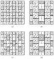
도 3 및 도 4는 본 발명의 일 실시예에 따라 형성된 유기 발광 소자의 전압-전류 그래프 및 전류 효율-휘도 특성을 비교예와 함께 각각 도시한 도면이다.
도 5는 본 발명의 일 실시예에 따른 유기 발광 소자에 적용할 수 있는 컬러 필터의 패턴 유형을 나타내는 도면이다.1 is a schematic cross-sectional view of an organic light emitting display device according to an embodiment of the present invention.
2 is a schematic cross-sectional view of an organic light emitting display device according to another embodiment of the present invention.
3 and 4 are diagrams illustrating a voltage-current graph and a current efficiency-luminance characteristic of an organic light emitting diode formed according to an embodiment of the present invention, respectively, with a comparative example.
5 is a diagram illustrating a pattern type of a color filter applicable to an organic light emitting diode according to an embodiment of the present invention.
이하 본 발명의 바람직한 실시예가 첨부된 도면들을 참조하여 설명될 것이다. 도면상의 동일한 부호는 동일한 요소를 지칭한다. 하기에서 본 발명을 설명함에 있어, 관련된 공지 기능 또는 구성에 대한 구체적인 설명이 본 발명의 요지를 불필요하게 흐릴 수 있다고 판단되는 경우에는 그 상세한 설명을 생략할 것이다.DETAILED DESCRIPTION OF THE PREFERRED EMBODIMENTS Hereinafter, preferred embodiments of the present invention will be described with reference to the accompanying drawings. Like reference numerals in the drawings refer to like elements. In the following description of the present invention, if it is determined that a detailed description of a related known function or configuration may unnecessarily obscure the subject matter of the present invention, the detailed description thereof will be omitted.
본 발명의 실시예를 설명하는 도면에 있어서, 어떤 층이나 영역들은 명세서의 명확성을 위해 두께를 확대하여 나타내었다. 또한 층, 막, 영역, 판 등의 부분이 다른 부분 "위에" 있다고 할 때, 이는 다른 부분 "바로 위에" 있는 경우뿐만 아니라 그 중간에 또 다른 부분이 있는 경우도 포함한다.In the drawings illustrating embodiments of the present invention, certain layers or regions are shown in enlarged thickness for clarity of specification. Also, when a portion of a layer, film, region, plate, etc. is said to be "on top" of another part, this includes not only when the other part is "right over" but also another part in the middle.
본 발명은 독립발광방식의 전면 및 배면 공진 구조를 갖는 유기 전계 발광 소자 제조 공정시, 수명 및 발광효율이 우수한 적색 발광층과 녹색 발광층을 스택(stack) 방식을 사용하여, 미세패턴 메탈 마스크(FMM)의 사용 횟수를 감소할 수 있는 방법을 제안한다.The present invention is a micro pattern metal mask (FMM) using a stacking method of a red light emitting layer and a green light emitting layer having excellent lifespan and luminous efficiency in a process of manufacturing an organic light emitting device having an independent emission type front and rear resonance structures. We propose a method that can reduce the number of times of use.
도 1은 본 발명의 일 실시예에 따른 유기 발광 디스플레이 장치의 개략적인 단면도이다.1 is a schematic cross-sectional view of an organic light emitting display device according to an embodiment of the present invention.
도 1을 참조하면, 본 발명의 유기 발광 소자는 기판(100) 및 기판(100)에 형성된 적색(R), 녹색(G) 및 청색(B) 서브 픽셀 영역들을 포함한다.Referring to FIG. 1, the organic light emitting diode of the present invention includes the
기판(100)은 투명한 글라스재, 플라스틱재, 또는 금속 호일 등을 사용할 수 있으며, 이에 한정되지 않고 기계적 강도, 열적 안정성, 투명성, 표면 평활성, 취급용이성 및 방수성이 우수한 통상적인 유기 발광 소자에서 사용되는 기판이 사용될 수 있다. 도면으로 도시하지는 않았지만, 상기 기판(100)은 각 서브 픽셀(R,G,B)마다 적어도 하나 이상의 박막 트랜지스터 및/또는 커패시터를 포함할 수 있고, 이러한 박막 트랜지스터 및 커패시터를 이용해 픽셀 회로를 구현할 수 있다.The
기판(100) 상부에는 서로 대향된 제1전극(120) 및 제2전극(140)을 구비한다. 상기 제1전극(120)은 적색(R), 녹색(G) 및 청색(B) 서브 픽셀 별로 패터닝될 수 있으며, 애노드 또는 캐소드일 수 있다. 상기 제2전극(140)은 제1전극(120)과 대응하여 캐소드 또는 애노드일 수 있다. 상기 제2전극(140)은 진공증착법이나 스퍼터링법 등을 이용하여 전자 주입층(136) 상부에 형성될 수 있다.The
기판(100)의 방향으로 화상이 구현되는 배면 발광형(bottom emission type)일 경우, 제1전극(120)은 투명 전극이 되고, 제2전극(140)은 반사전극이 될 수 있다. 제1전극(120)은 일함수가 높은 ITO, IZO, ZnO, 또는 In2O3 등으로 형성하고, 제2전극(140)은 일함수가 작은 금속 즉, Ag, Mg, Al, Pt, Pd, Au, Ni, Nd, Ir, Cr, Li, Ca 등으로 형성할 수 있다.In the case of a bottom emission type in which an image is implemented in the direction of the
제2전극(140)의 방향으로 화상을 구현하는 전면 발광형(top emission type)일 경우, 제1전극(120)은 반사 전극으로 구비될 수 있고, 제2전극(140)은 투명 전극으로 구비될 수 있다. 이때, 제1전극(120)이 되는 반사 전극은 Ag, Mg, Al, Pt, Pd, Au, Ni, Nd, Ir, Cr, Li, Ca 및 이들의 화합물 등으로 반사막을 형성한 후, 그 위에 일함수가 높은 ITO, IZO, ZnO, 또는 In2O3 등을 형성하여 이루어질 수 있다. 그리고, 제2전극(140)이 되는 투명 전극은, 일함수가 작은 금속 즉, Ag, Mg, Al, Pt, Pd, Au, Ni, Nd, Ir, Cr, Li, Ca 및 이들의 화합물을 증착한 후, 그 위에 ITO, IZO, ZnO, 또는 In2O3 등의 투명 도전물질로 보조 전극층이나 버스 전극 라인을 형성할 수 있다.In the case of a top emission type that implements an image in the direction of the
양면 발광형의 경우, 제1전극(120)과 제2전극(140) 모두를 투명 전극으로 형성할 수 있다.In the case of the double-sided light emission type, both the
한편, 전술한 바와 같이 기판(100)이 박막 트랜지스터를 포함할 경우, 서브 픽셀별로 패터닝된 제1전극(120)은 각 서브 픽셀의 박막 트랜지스터에 전기적으로 연결된다. 그리고, 이때, 제2전극(140)은 모든 서브 픽셀에 걸쳐 서로 연결되어 있는 공통전극으로 형성될 수 있다.Meanwhile, as described above, when the
기판(100)이 서브 픽셀별로 박막 트랜지스터를 포함하지 않을 경우 제1전극(120)과 제2전극(140)은 서로 교차되는 스트라이프 패턴으로 패터닝되어 PM(Passive Matrix) 구동할 수 있다.When the
상기 제1전극(120)과 제2전극(140) 사이에는 유기막(130)이 개재된다. 유기막(130)은 정공 주입층(131), 보조층(132R), 정공 수송층(133), 적색 발광층(134R), 녹색 발광층(134G), 청색 발광층(134B), 전자 수송층(135), 및 전자 주입층(136)을 차례로 구비한다.An
상기 제1전극(120) 상부에는 도면에는 도시되지 않았으나, 상기 제1전극의 상단부 및 측면을 덮는 화소정의막이 형성될 수 있다. 상기 화소정의막은 유기물, 무기물, 또는 유무기물 복합 다층 구조로 형성될 수 있다. 무기물로서는 실리콘 산화물(SiO2), 실리콘 질화물(SiNx), 실리콘 산화질화물 등의 무기물 중에서 선택된 물질을 사용할 수 있다. 유기물로서는아크릴(Acryl)계 유기화합물, 폴리아미드, 폴리이미드 등의 유기 절연물질 중 하나일 수 있다.Although not shown in the drawing, a pixel defining layer may be formed on the
상기 제1전극(120)이 형성된 기판(100) 상부에 오픈 마스크(open mask)를 사용하여 정공 주입층(HIL)(131)이 적색(R), 녹색(G), 청색(B) 서브 픽셀에 대하여 공통층으로 형성된다. 정공 주입층(131)은 정공이 용이하게 주입되도록 약 300Å~ 800Å의 두께로 형성될 수 있는데, 이는 다른 층의 재료에 따라 가변 가능하다. 정공 주입층(131)은 2-TNATA, 구리 프탈로시아닌(CuPc) 또는 스타버스트(Starburst)형 아민류인 TCTA, m-MTDATA, IDE406 (이데미쯔사 재료) 등을 사용할 수 있으며, 정공의 주입을 돕는 물질이라면 이에 한정되지 않고 사용될 수 있다.A hole injection layer (HIL) 131 is formed of red (R), green (G), and blue (B) subpixels using an open mask on the
상기 정공 주입층(131) 상부에 정공 이동도가 좋으며 정공의 수송을 용이하게 하는 정공 수송층(HTL)(133)이 형성된다.A hole transport layer (HTL) 133 is formed on the
상기 정공 수송층(133)은 오픈 마스크를 사용하여 적색(R), 녹색(G), 청색(B) 서브 픽셀에 대하여 공통층으로 형성된다. 정공 수송층(133)의 두께는 약 300Å~800Å일 수 있는데, 이는 다른 층의 재료에 따라 가변 가능하다. 정공 수송층(133)의 증착조건 및 코팅조건은 사용하는 화합물에 따라 다르지만, 일반적으로 정공 주입층(131)의 형성과 거의 동일한 조건범위 중에서 선택될 수 있다. 상기 정공 수송층(133)의 물질은 특별히 제한되지 않으며, N-페닐카르바졸, 폴리비닐카르바졸 등의 카르바졸 유도체, 4,4'-비스[N-(1-나프틸)-N-페닐아미노]비페닐(NPB), N,N'-비스(3-메틸페닐)-N,N'-디페닐-[1,1-비페닐]-4,4'-디아민(TPD), N,N'-디(나프탈렌-1-일)-N,N'-디페닐 벤지딘(α-NPD), IDE 320(이데미쯔사 재료) 등이 사용될 수 있다.The
적색 서브 픽셀(R) 영역의 상기 정공 주입층(131) 및 정공 수송층(133) 사이에는 보조층(132R)이 추가 구비된다. 상기 보조층(132R)은 적색 서브 픽셀(R) 영역의 정공 주입층(131)과 정공 수송층(133) 사이에서 적색 광의 공진 주기 조절을 위해 구비된다.An
상기 보조층(132R)은 적색 광의 공진 주기를 조절하기 위하여 적색 서브 픽셀(R)의 유기층 두께를 맞춰주는 역할을 한다. 보조층(132R)은 적색 광의 발광 효율, 색순도 등을 높일 수 있도록, 300 내지 1500Å 범위의 두께로 설정될 수 있다. 상기 보조층(132R)은 FMM(Fine Metal Mask)을 사용하여 적색 서브 픽셀(R) 영역에만 형성될 수 있다. 상기 보조층(132R)을 이루는 물질은 상기 정공 수송층(133)의 물질과 동일한 물질로 형성될 수 있다.The
상기 정공 수송층(133) 상부에는 발광층(134)이 형성된다. 발광층(134)은 적색 서브 픽셀(R) 영역 및 녹색 서브 픽셀(G) 영역에 차례로 적층되는 적색 발광층(134R) 및 녹색 발광층(134G)과, 청색 서브 픽셀(B) 영역에 구비되는 청색 발광층(134B)을 포함한다. 즉, 적색 발광층(134R) 및 녹색 발광층(134G)은 스택(stack) 방식으로 적색 서브 픽셀(R) 영역과 녹색 서브 픽셀(G) 영역에 공통으로 구비된다.The emission layer 134 is formed on the
적색 발광층(134R), 녹색 발광층(134G) 및 청색 발광층(134B)은 정공 수송층(133) 상부에 FMM(Fine Metal Mask)을 사용하여 형성될 수 있다. 이때 적색 발광층(134R)과 녹색 발광층(134G)은 적색 서브 픽셀(R)과 녹색 서브 픽셀(G) 영역에 공통층으로 차례로 적층된다. 따라서 각 서브 픽셀에 개별적으로 발광층을 형성하는 경우에 비해 더 큰 개구부를 갖는 마스크를 사용할 수 있기 때문에 대형 마스크 제작에 유리하다. 청색 발광층(134B)은 FMM을 사용하여 청색 서브 픽셀(B) 영역에만 적층된다.The red light emitting layer 134R, the green
전술된 보조층(132R)은 적색 서브 픽셀(R)에 구비하여 적색광의 공진 주기를 조절하고, 상기 적색 발광층(134R)은 적색 서브 픽셀(R) 및 녹색 서브 픽셀(G)에 구비하여 녹색 서브 픽셀(G)의 녹색광 공진 주기를 조절한다. 따라서 적색 발광층(134R)은 적색광의 발광 및 녹색 서브 픽셀(G)의 보조층 역할을 동시에 하게 된다. 상기 적색 발광층(134R)은 정공 수송능을 갖고, 상기 녹색 발광층(134G)은 전자 수송능을 갖는다.The
상기 발광층들은 공지된 다양한 발광 물질을 이용하여 형성할 수 있는데, 공지의 호스트 및 도펀트를 이용하여 형성할 수도 있다. 상기 도펀트의 경우, 공지의 형광 도펀트 및 공지의 인광 도펀트를 모두 사용할 수 있다. 특히, 적색 발광층(134R)은 정공 전송 특성이 우수한 호스트와 적색 도판트를 포함하는 것이 바람직하고, 녹색 발광층(134G)은 전자 전송 특성이 우수한 호스트와 그린 도판트를 포함하는 것이 바람직하다.The light emitting layers may be formed using various known light emitting materials, and may be formed using known hosts and dopants. In the case of the above-mentioned dopant, a known fluorescent dopant and a known phosphorescent dopant can be used. In particular, the red light emitting layer 134R preferably includes a host and a red dopant having excellent hole transport characteristics, and the green
상기 발광층(134)의 호스트로서는 Alq3, CBP(4,4'-N,N'-디카바졸-비페닐), PVK(폴리(n-비닐카바졸)), DSA(디스티릴아릴렌), 그라셀사의 GDI1403(적색 인광 호스트), 그라셀사의 GGH01(녹색 형광 호스트) 등을 사용할 수 있으나 이에 한정되는 것은 아니다.Examples of the host of the light emitting layer 134 include Alq3, CBP (4,4'-N, N'-dicarbazole-biphenyl), PVK (poly (n-vinylcarbazole)), DSA (distyrylarylene), and graphene. Cell's GDI1403 (red phosphorescent host), Glass's GGH01 (green fluorescent host) and the like can be used, but is not limited thereto.
상기 발광층(134)의 도펀트의 함량은 발광층 형성재료 100 중량부 (즉, 호스트와 도펀트의 총중량은 100중량부로 함)를 기준으로 하여 0.1 내지 20 중량부, 특히 0.5 ~ 15 중량부인 것이 바람직하다. 도펀트의 함량이 0.1 중량부 미만이면 도펀트 부가에 따른 효과가 미미하고 20 중량부를 초과하면 인광이나 형광 모두 다 농도 켄칭(quenching)과 같은 농도 소광이 일어나 바람직하지 못하다.The dopant content of the light emitting layer 134 is preferably 0.1 to 20 parts by weight, particularly 0.5 to 15 parts by weight based on 100 parts by weight of the light emitting layer forming material (ie, the total weight of the host and the dopant is 100 parts by weight). If the content of the dopant is less than 0.1 parts by weight, the effect of the addition of the dopant is insignificant, and if it exceeds 20 parts by weight, concentration phosphorescence or fluorescence, such as concentration quenching (quenching) is not preferable because it occurs.
발광 효율을 고려하여, 상기 적색 발광층(134R)의 두께는 500 내지 2000Å, 녹색 발광층(134G)은 100 내지 1000Å, 청색 발광층(134B)은 200 내지 1000Å일 수 있다.In consideration of the light emitting efficiency, the red light emitting layer 134R may have a thickness of 500 to 2000 mW, the green
상기 발광층(134) 상부에는 전자 수송층(ETL)(135)이 형성된다.An electron transport layer (ETL) 135 is formed on the emission layer 134.
상기 전자 수송층(135)은 상기 녹색 발광층(134G) 및 청색 발광층(134B) 상부에 오픈 마스크를 사용하여 기판 전면에 형성된다. 전자 수송층(135)의 두께는 200 내지 500Å일 수 있는 데, 이는 다른 층의 재료에 따라 가변 가능하다. 전자 수송층(135)은 전자 수송을 용이하게 하여 효율적인 전자 수송을 제공할 수 있도록 한다. 전자 수송층(135)의 물질은 특별히 한정되지 않으며, 공지된 전자 수송층 형성 재료 중에서 임의로 선택될 수 있다. 예를 들면, 퀴놀린 유도체, 특히 트리스(8-퀴놀리노레이트)알루미늄(Alq3), TAZ 등과 같은 공지의 재료를 이용할 수 있다.The
상기 전자 주입층(136)은 상기 전자 수송층(135) 상부에 오픈 마스크를 사용하여 기판 전면에 형성된다. 전자 주입층(136)의 두께는 5 내지 50Å일 수 있는 데, 이는 다른 층의 재료에 따라 가변 가능하다. 전자 주입층(136)은 제2전극(140)으로부터 전자의 주입을 용이하게 하는 기능을 가지는 물질이 사용될 수 있으며, LiF, NaCl, CsF, Li2O, BaO, Liq 등과 같은 임의의 물질을 이용할 수 있다.The
한편, 비록 도면으로 도시하지는 않았지만, 상기 발광층(134)과 전자 수송층(135) 사이에는 정공 저지용 물질을 사용하여 정공 저지층(HBL)을 선택적으로 형성할 수 있다. 이때 사용되는 정공 저지층 형성용 물질은 특별히 제한되지는 않으나, 전자 수송 능력을 가지면서 발광 화합물보다 높은 이온화 퍼텐셜을 가져야 하며 대표적으로 Balq, BCP, TPBI 등이 사용될 수 있다.Although not shown in the drawings, a hole blocking layer HBL may be selectively formed between the light emitting layer 134 and the
전술한 바와 같이 상기 실시예에서는 적색 발광층(134R)과 녹색 발광층(134G)을 적층 방식으로 적색 서브 픽셀(R) 영역과 녹색 서브 픽셀(G) 영역에 공통층으로 구비된다. 따라서, 녹색 서브 픽셀(G) 영역에 보조층을 형성하기 위한 추가 FMM 사용이 불필요해지기 때문에, 4회의 FMM의 사용으로 공정을 단순화시킬 수 있다.As described above, the red light emitting layer 134R and the green
도 2는 본 발명의 다른 실시예에 따른 유기 발광 디스플레이 장치의 개략적인 단면도이다.2 is a schematic cross-sectional view of an organic light emitting display device according to another embodiment of the present invention.
본 실시예의 유기 발광 디스플레이 장치는 도 1의 유기 발광 디스플레이 장치와 마찬가지로 기판(200) 및 기판(200)에 형성된 적색(R), 녹색(G) 및 청색(B) 서브 픽셀 영역들을 포함하며, 청색 발광층(234B)이 공통층(common layer)으로 형성되는 점이 상이하다. 따라서, 도 1의 유기 발광 디스플레이 장치와 중복되는 구조와 그에 대응하는 제조 공정의 상세한 설명은 생략하겠다.The organic light emitting diode display according to the present exemplary embodiment includes red (R), green (G), and blue (B) subpixel regions formed on the
도 2를 참조하면, 기판(200) 상부에 제1전극(220)과 제1전극(240)에 대향하는 제2전극(140)이 구비된다. 상기 제1전극(220)과 제2전극(240) 사이에는 정공 주입층(231), 보조층(232R), 정공 수송층(233), 적색 발광층(234R), 녹색 발광층(234G), 청색 발광층(234B), 전자 수송층(235), 및 전자 주입층(236)을 포함하는 유기막(230)이 개재된다.2, a
상기 제1전극(220)은 적색(R), 녹색(G) 및 청색(B) 서브 픽셀 별로 이격되어 형성된다. 상기 제1전극(220) 상부에는 도면에는 도시되지 않았으나, 상기 제1전극(220)의 상단부 및 측면을 덮는 화소정의막이 형성될 수 있다.The
상기 제1전극(220) 상부에 상기 정공 주입층(231) 및 정공 수송층(233)이 오픈 마스크를 사용하여 차례로 적층된다.The
상기 보조층(232R)은 적색 서브 픽셀(R) 영역의 정공 주입층(231)과 정공 수송층(233) 사이에 구비되며, 적색 광의 공진 주기 조절을 위해 구비된다. 상기 보조층(232R)은 FMM을 사용하여 상기 정공 주입층(231) 상부에 형성된다.The
상기 정공 수송층(233) 상부에는 발광층(234)이 형성된다.The emission layer 234 is formed on the hole transport layer 233.
적색 발광층(234R)은 적색 서브 픽셀(R) 영역과 녹색 서브 픽셀(G) 영역에서 정공 수송층(233) 상부에 FMM을 사용하여 형성된다.The red
녹색 발광층(234G)은 적색 서브 픽셀(R) 영역과 녹색 서브 픽셀(G) 영역에서 적색 발광층(234R) 상부에 FMM을 사용하여 형성된다. 즉, 적색 발광층(234R)과 녹색 발광층(234G)은 적색 서브 픽셀(R) 영역과 녹색 서브 픽셀(G) 영역에 공통층으로 형성된다. 적색 발광층(234R)은 적색 서브 픽셀(R) 영역에서는 발광층으로, 녹색 서브 픽셀(G) 영역에서는 정공 수송의 역할을 하게 된다.The green light emitting layer 234G is formed using the FMM on the red
청색 발광층(234B)은 적색 서브 픽셀(R) 영역과 녹색 서브 픽셀(G) 영역의 녹색 발광층(234G) 상부와, 청색 서브 픽셀(B) 영역의 정공 수송층(233) 상부에 형성된다. 즉 청색 발광층(234B)은 오픈 마스크를 사용하여 기판 전면에 공통층으로 형성된다. 따라서 청색 발광층(234B)의 형성시 FMM 대신 개구부가 더 큰 오픈 마스크를 사용하기 때문에, 도 1의 유기 발광 디스플레이 장치보다 FMM의 사용 횟수를 3회로 줄일 수 있어 공정을 단순화시킬 수 있다. 청색 발광층(234B)은 100 내지 500Å 두께로 형성될 수 있다. 적색 발광층(234R)은 500 내지 2000Å 두께로, 녹색 발광층(234G)은 200 내지 1000Å 두께로 형성될 수 있다.The blue
상기 발광층(234) 상부에는 전자 수송층(235)이 오픈 마스크를 사용하여 기판 전면에 형성된다.The
상기 전자 수송층(235) 상부에는 전자 주입층(236)이 오픈 마스크를 사용하여 기판 전면에 형성된다.An electron injection layer 236 is formed on the entire surface of the substrate using an open mask on the
도면으로 도시하지는 않았지만, 상기 발광층(234)과 전자 수송층(235) 사이에는 정공 저지용 물질을 사용하여 정공 저지층(HBL)을 선택적으로 형성할 수 있다.Although not shown in the drawings, a hole blocking layer HBL may be selectively formed between the light emitting layer 234 and the
상기 전자 주입층(236) 상부에는 제2전극(240)이 형성되며, 상기 제2전극(240)은 모든 서브 픽셀에 걸쳐 서로 연결되어 있는 공통전극으로 형성될 수 있다.A
도 3 및 도 4는 본 발명의 일 실시예에 따라 형성된 유기 발광 소자의 전압-전류 그래프 및 전류 효율-휘도 특성을 비교예와 함께 각각 도시한 도면이다.3 and 4 are diagrams illustrating a voltage-current graph and a current efficiency-luminance characteristic of an organic light emitting diode formed according to an embodiment of the present invention, respectively, with a comparative example.
도 3 및 도 4에는, 적색 발광층과 녹색 발광층이 스택 구조로 형성되고(RG 스택), 공통 청색 발광층(Blue Common Layer: BCL) 구조인 본 발명의 도 2에 도시된 실시예와, RG 스택 및 BCL 구조에 녹색 보조층(G보조층)이 추가된 비교예의 데이터가 함께 도시되어 있다.3 and 4, the red light emitting layer and the green light emitting layer are formed in a stack structure (RG stack), the embodiment shown in FIG. 2 of the present invention having a common blue light emitting layer (Blue Common Layer (BCL)) structure, an RG stack, and The data of the comparative example in which the green auxiliary layer (G auxiliary layer) is added to the BCL structure is shown together.
도 3 및 도 4를 참조하면, 본 발명에 의해 제작된 RG 스택 유기 발광 소자는 구동전압이 낮은 고효율 소자이고, 휘도 증가에 따라서 색도 변화가 작고, 오랜 구동 후에도 성능저하가 크지 않은 우수하고, 안정한 소자 특성을 가지게 된다. 또한, 적색 발광층을 사용하여 적색 서브 픽셀에서는 적색 발광을 하고, 녹색 서브 픽셀에서는 G보조층으로 사용함으로써, 별도의 G보조층을 구비한 경우에 비해 효율 및 전압에서 크게 차이가 없으며, 공정상의 단순화를 꾀할 수 있는 장점이 있다.3 and 4, the RG stack organic light emitting device manufactured by the present invention is a high efficiency device having a low driving voltage, a small change in chromaticity according to the increase in luminance, and excellent and stable with no significant performance degradation even after long driving. Device characteristics. In addition, by using the red light emitting layer to emit red light in the red subpixel and the green subpixel as the G sublayer, there is no significant difference in efficiency and voltage as compared to the case where a separate G sublayer is provided, and the process is simplified. There is an advantage to try.
도 5는 본 발명의 일 실시예에 따른 유기 발광 소자에 적용할 수 있는 컬러 필터의 패턴 유형을 나타내는 도면이다.5 is a diagram illustrating a pattern type of a color filter applicable to an organic light emitting diode according to an embodiment of the present invention.
도 5를 참조하면, 본 발명은 적색 발광층과 녹색 발광층을 스택 방식으로 형성하기 때문에, 봉지(Encapsulation)용 커버 글래스 기판 상에 (a) 내지 (d)에 도시된 바와 같이 적색 및 녹색 필터 패턴을 인접하게 형성할 수 있다.Referring to FIG. 5, since the red light emitting layer and the green light emitting layer are formed in a stacking manner, the red and green filter patterns may be formed on the cover glass substrate for encapsulation as shown in (a) to (d). It can be formed adjacently.
본 발명은 도면에 도시된 실시예를 참고로 설명되었으나 이는 예시적인 것에 불과하며, 당해 기술 분야에서 통상의 지식을 가진 자라면 이로부터 다양한 변형 및 균등한 다른 실시예가 가능하다는 점을 이해할 것이다. 따라서, 본 발명의 진정한 기술적 보호 범위는 첨부된 특허청구범위의 기술적 사상에 의하여 정해져야 할 것이다.While the present invention has been described with reference to exemplary embodiments, it is to be understood that the invention is not limited to the disclosed exemplary embodiments, but, on the contrary, is intended to cover various modifications and equivalent arrangements included within the spirit and scope of the invention. Accordingly, the true scope of the present invention should be determined by the technical idea of the appended claims.
Claims (21)
Translated fromKorean상기 제1전극을 덮도록 상기 기판 상부에 구비된 정공 주입층;
상기 정공 주입층 상부에 구비된 정공 수송층;
상기 적색 서브 픽셀의 상기 정공 주입층 및 상기 정공 수송층 사이에 상기 적색 서브 픽셀의 적색 광의 공진 주기를 조절하기 위해 구비되는 보조층; 및
상기 적색 서브 픽셀과 상기 녹색 서브 픽셀의 상기 정공 수송층 상부에 차례로 형성된 적색 발광층과 녹색 발광층, 및 상기 청색 서브 픽셀의 상기 정공 수송층 상부와 상기 녹색 발광층 상부에 구비된 청색 발광층;을 포함하는 것을 특징으로 하는 유기 발광 디스플레이 장치.A first electrode provided in the red, green, and blue subpixels on the substrate;
A hole injection layer provided on the substrate to cover the first electrode;
A hole transport layer provided on the hole injection layer;
An auxiliary layer provided between the hole injection layer of the red subpixel and the hole transport layer to adjust a resonance period of red light of the red subpixel; And
And a red light emitting layer and a green light emitting layer sequentially formed on the hole transport layer of the red subpixel and the green subpixel, and a blue light emitting layer provided on the hole transport layer and the green light emitting layer of the blue subpixel. Organic light emitting display device.
상기 적색 발광층은 정공 수송능을 갖고, 상기 녹색 발광층은 전자 수송능을 갖는 것을 특징으로 하는 유기 발광 디스플레이 장치.The method of claim 1,
And the red light emitting layer has a hole transporting capability, and the green light emitting layer has an electron transporting capability.
상기 보조층은 정공 수송능을 갖는 것을 특징으로 하는 유기 발광 디스플레이 장치.The method of claim 1,
And the auxiliary layer has a hole transporting ability.
상기 보조층은 두께가 300Å 내지 1500Å인 것을 특징으로 하는 유기 발광 디스플레이 장치.The method of claim 1,
And the auxiliary layer has a thickness of 300 mW to 1500 mW.
상기 적색 발광층은 두께가 500Å 내지 2000Å이고, 녹색 발광층은 100Å 내지 1000Å인 것을 특징으로 하는 유기 발광 디스플레이 장치.The method of claim 1,
The red light emitting layer has a thickness of 500 kPa to 2000 kPa, and the green light emitting layer is 100 kPa to 1000 kPa.
상기 청색 발광층의 두께가 100Å 내지 500Å인 것을 특징으로 하는 유기 발광 디스플레이 장치.The method of claim 1,
An organic light emitting display device, characterized in that the thickness of the blue light emitting layer is 100 kPa to 500 kPa.
상기 보조층은 상기 정공 수송층과 동일한 물질로 형성되는 것을 특징으로 하는 유기 발광 디스플레이 장치.The method of claim 1,
And the auxiliary layer is formed of the same material as that of the hole transport layer.
상기 제1전극을 덮도록 상기 기판 상부에 정공 주입층을 형성하는 단계;
상기 적색 서브 픽셀의 상기 정공 주입층 상부에 상기 적색 서브 픽셀의 적색 광의 공진 주기를 조절하기 위한 보조층을 형성하는 단계;
상기 보조층을 덮도록 상기 정공 주입층 상부에 정공 수송층을 형성하는 단계;
상기 적색 서브 픽셀과 상기 녹색 서브 픽셀의 상기 정공 수송층 상부에 적색 발광층과 녹색 발광층을 차례로 형성하는 단계; 및
상기 녹색 발광층 상부를 포함하여 상기 기판 전면에 청색 발광층을 공통층으로 형성하는 단계;를 포함하는 것을 특징으로 하는 유기 발광 디스플레이 장치 제조 방법.Forming a red, green, and blue subpixel first electrode on the substrate;
Forming a hole injection layer on the substrate to cover the first electrode;
Forming an auxiliary layer on the hole injection layer of the red subpixel to adjust a resonance period of the red light of the red subpixel;
Forming a hole transport layer on the hole injection layer to cover the auxiliary layer;
Sequentially forming a red light emitting layer and a green light emitting layer on the hole transport layer of the red sub pixel and the green sub pixel; And
Forming a blue light emitting layer as a common layer on the entire surface of the substrate, including the green light emitting layer.
상기 적색 발광층은 정공 수송능을 갖고, 상기 녹색 발광층은 전자 수송능을 갖는 것을 특징으로 하는 유기 발광 디스플레이 장치 제조 방법.10. The method of claim 9,
And the red light emitting layer has a hole transporting ability, and the green light emitting layer has an electron transporting ability.
상기 보조층은 정공 수송능을 갖는 것을 특징으로 하는 유기 발광 디스플레이 장치 제조 방법.10. The method of claim 9,
The auxiliary layer has a hole transporting ability, characterized in that the organic light emitting display device manufacturing method.
상기 보조층은 두께가 300Å 내지 1500Å인 것을 특징으로 하는 유기 발광 디스플레이 장치 제조 방법.10. The method of claim 9,
And the auxiliary layer has a thickness of 300 mW to 1500 mW.
상기 적색 발광층은 두께가 500Å 내지 2000Å이고, 녹색 발광층은 100Å 내지 1000Å인 것을 특징으로 하는 유기 발광 디스플레이 장치 제조 방법.10. The method of claim 9,
The red light emitting layer has a thickness of 500 kPa to 2000 kPa, and the green light emitting layer is 100 kPa to 1000 kPa.
상기 청색 발광층의 두께가 100Å 내지 500Å인 것을 특징으로 하는 유기 발광 디스플레이 장치 제조 방법.10. The method of claim 9,
The blue light emitting layer has a thickness of 100 kPa to 500 kPa.
상기 보조층은 상기 정공 수송층과 동일한 물질로 형성되는 것을 특징으로 하는 유기 발광 디스플레이 장치 제조 방법.10. The method of claim 9,
The auxiliary layer is formed of the same material as the hole transport layer manufacturing method of an organic light emitting display device.
상기 보조층은 미세패턴 메탈 마스크(FMM)에 의해 패터닝하여 형성되는 것을 특징으로 하는 유기 발광 디스플레이 장치 제조 방법.10. The method of claim 9,
And the auxiliary layer is formed by patterning by a fine pattern metal mask (FMM).
상기 적색 발광층 및 상기 녹색 발광층은 미세패턴 메탈 마스크(FMM)에 의해 패터닝하여 형성되는 것을 특징으로 하는 유기 발광 디스플레이 장치 제조 방법.10. The method of claim 9,
The red light emitting layer and the green light emitting layer is a method of manufacturing an organic light emitting display device, characterized in that formed by patterning with a fine pattern metal mask (FMM).
상기 청색 발광층은 오픈 마스크에 의해 패터닝하여 형성되는 것을 특징으로 하는 유기 발광 디스플레이 장치 제조 방법.10. The method of claim 9,
The blue light emitting layer is a method of manufacturing an organic light emitting display device, characterized in that formed by patterning with an open mask.
Priority Applications (6)
| Application Number | Priority Date | Filing Date | Title |
|---|---|---|---|
| KR1020100007444AKR101182442B1 (en) | 2010-01-27 | 2010-01-27 | OLED display apparatus and Method thereof |
| JP2011002335AJP5783727B2 (en) | 2010-01-27 | 2011-01-07 | Organic light emitting display device and method for manufacturing the same |
| US12/929,459US8471275B2 (en) | 2010-01-27 | 2011-01-26 | Organic light emitting device display and method of manufacturing the same |
| TW100102970ATWI540938B (en) | 2010-01-27 | 2011-01-26 | Display of organic light emitting element and method of manufacturing same |
| CN201110032384.1ACN102163615B (en) | 2010-01-27 | 2011-01-27 | Organic light emitting device display and manufacture method thereof |
| JP2015103105AJP2015146468A (en) | 2010-01-27 | 2015-05-20 | Organic light-emitting display device |
Applications Claiming Priority (1)
| Application Number | Priority Date | Filing Date | Title |
|---|---|---|---|
| KR1020100007444AKR101182442B1 (en) | 2010-01-27 | 2010-01-27 | OLED display apparatus and Method thereof |
Publications (2)
| Publication Number | Publication Date |
|---|---|
| KR20110087829A KR20110087829A (en) | 2011-08-03 |
| KR101182442B1true KR101182442B1 (en) | 2012-09-12 |
Family
ID=44308299
Family Applications (1)
| Application Number | Title | Priority Date | Filing Date |
|---|---|---|---|
| KR1020100007444AActiveKR101182442B1 (en) | 2010-01-27 | 2010-01-27 | OLED display apparatus and Method thereof |
Country Status (5)
| Country | Link |
|---|---|
| US (1) | US8471275B2 (en) |
| JP (2) | JP5783727B2 (en) |
| KR (1) | KR101182442B1 (en) |
| CN (1) | CN102163615B (en) |
| TW (1) | TWI540938B (en) |
Cited By (10)
| Publication number | Priority date | Publication date | Assignee | Title |
|---|---|---|---|---|
| US9780148B2 (en) | 2014-08-20 | 2017-10-03 | Samsung Display Co., Ltd. | Display device and method for manufacturing the same |
| KR20190004412A (en) | 2017-07-03 | 2019-01-14 | 한국생산기술연구원 | Donor substrate having a light to heat conversion layer and hydrophobic thin film patterns, donor substrate having light to heat conversion patterns and hydrophobic thin film patterns, method of forming light emitting patterns by using a donor substrate, light emitting pattern, and light emitting diode |
| KR20190004413A (en) | 2017-07-03 | 2019-01-14 | 한국생산기술연구원 | Donor substrate having groove patterns, method of forming light emitting patterns by heating the same, light emitting pattern, and light emitting diode |
| KR20190033106A (en) | 2017-09-20 | 2019-03-29 | 한국생산기술연구원 | Donor substrate assembly having recessed unit and method of manufacturing light emitting diode using same |
| KR20190033105A (en) | 2017-09-20 | 2019-03-29 | 한국생산기술연구원 | Organic light-emitting display manufacturing apparatus using donor substrate and manufacturing method thereof |
| WO2021137463A1 (en)* | 2019-12-31 | 2021-07-08 | 주식회사 토비스 | Double-sided organic light-emitting display device |
| KR20220043963A (en) | 2020-09-28 | 2022-04-06 | 한국생산기술연구원 | Method of manufacturing donor substrate for high-resolution OLED pattern formation, donor substrate and forming method for high-resolution OLED pattern |
| US12075659B2 (en) | 2020-10-20 | 2024-08-27 | Samsung Display Co., Ltd. | Display apparatus and method of manufacturing the same |
| US12408280B2 (en) | 2022-03-15 | 2025-09-02 | Samsung Display Co., Ltd. | Circuit board and display device including the same |
| US12433138B2 (en) | 2019-12-20 | 2025-09-30 | Samsung Display Co., Ltd. | Organic light-emitting display device and method for manufacturing the same |
Families Citing this family (81)
| Publication number | Priority date | Publication date | Assignee | Title |
|---|---|---|---|---|
| CA2419704A1 (en) | 2003-02-24 | 2004-08-24 | Ignis Innovation Inc. | Method of manufacturing a pixel with organic light-emitting diode |
| CA2495726A1 (en) | 2005-01-28 | 2006-07-28 | Ignis Innovation Inc. | Locally referenced voltage programmed pixel for amoled displays |
| JP2011523212A (en)* | 2008-06-05 | 2011-08-04 | スリーエム イノベイティブ プロパティズ カンパニー | Light emitting diode with semiconductor wavelength converter bonded |
| US8497828B2 (en) | 2009-11-12 | 2013-07-30 | Ignis Innovation Inc. | Sharing switch TFTS in pixel circuits |
| KR101257734B1 (en) | 2010-09-08 | 2013-04-24 | 엘지디스플레이 주식회사 | Organic Electroluminescent Display Device |
| CN103534833B (en)* | 2011-05-13 | 2016-07-20 | 索尼株式会社 | Organic Electroluminescent Multicolor Light-Emitting Device |
| CN109272933A (en) | 2011-05-17 | 2019-01-25 | 伊格尼斯创新公司 | The method for operating display |
| US9606607B2 (en) | 2011-05-17 | 2017-03-28 | Ignis Innovation Inc. | Systems and methods for display systems with dynamic power control |
| KR101858636B1 (en)* | 2011-06-14 | 2018-05-17 | 삼성디스플레이 주식회사 | Organic light emitting diode display |
| US8901579B2 (en) | 2011-08-03 | 2014-12-02 | Ignis Innovation Inc. | Organic light emitting diode and method of manufacturing |
| US9070775B2 (en) | 2011-08-03 | 2015-06-30 | Ignis Innovations Inc. | Thin film transistor |
| KR101821739B1 (en)* | 2011-08-25 | 2018-01-25 | 삼성디스플레이 주식회사 | Organic light emitting diode display and manufacturing method thereof |
| EP2579313B1 (en)* | 2011-09-22 | 2021-10-27 | LG Display Co., Ltd. | Organic light emitting diode display device and method of fabricating the same |
| JP5919723B2 (en)* | 2011-10-19 | 2016-05-18 | ソニー株式会社 | Display panel, display device and electronic device |
| KR101400389B1 (en)* | 2011-11-01 | 2014-05-28 | 엘지디스플레이 주식회사 | Organic light emitting diode |
| US9813695B2 (en)* | 2011-11-09 | 2017-11-07 | Koninklijke Philips N.V. | Display device with free focus capability |
| US10089924B2 (en) | 2011-11-29 | 2018-10-02 | Ignis Innovation Inc. | Structural and low-frequency non-uniformity compensation |
| US9385169B2 (en) | 2011-11-29 | 2016-07-05 | Ignis Innovation Inc. | Multi-functional active matrix organic light-emitting diode display |
| TW201324761A (en) | 2011-12-08 | 2013-06-16 | Au Optronics Corp | Pixel structure of electroluminescent display panel |
| KR101945930B1 (en)* | 2012-01-05 | 2019-02-11 | 삼성디스플레이 주식회사 | Organic light emitting device |
| KR20140141571A (en)* | 2012-03-07 | 2014-12-10 | 가부시키가이샤 가네카 | Method for manufacturing light-emitting device, and light-emitting device |
| US9190456B2 (en)* | 2012-04-25 | 2015-11-17 | Ignis Innovation Inc. | High resolution display panel with emissive organic layers emitting light of different colors |
| KR101952706B1 (en)* | 2012-07-24 | 2019-02-28 | 삼성디스플레이 주식회사 | Organic light-emitting device and organic light-emitting display apparatus including the same |
| KR20140024977A (en)* | 2012-08-17 | 2014-03-04 | 삼성디스플레이 주식회사 | Flat panel display device and manufacturing method thereof |
| KR101464270B1 (en)* | 2012-08-24 | 2014-11-21 | 엘지디스플레이 주식회사 | Organic light-emitting diode and method of fabricating the same |
| KR102000292B1 (en)* | 2012-09-07 | 2019-07-16 | 삼성디스플레이 주식회사 | Organic light emitting display device and method for manufacturing thereof |
| KR20230015519A (en)* | 2012-10-30 | 2023-01-31 | 가부시키가이샤 한도오따이 에네루기 켄큐쇼 | Light-emitting panel, display device, and method for manufacturing light-emitting panel |
| KR101429725B1 (en)* | 2012-10-31 | 2014-08-12 | 엘지디스플레이 주식회사 | Organic Light Emitting Display Device and fabricating method of the same |
| US8921842B2 (en)* | 2012-11-14 | 2014-12-30 | Lg Display Co., Ltd. | Organic light emitting display device and method of manufacturing the same |
| TWI503968B (en)* | 2012-11-29 | 2015-10-11 | Univ Yuan Ze | Reflective organic light emitting diode display device and driving method thereof |
| JP6111643B2 (en)* | 2012-12-17 | 2017-04-12 | セイコーエプソン株式会社 | ORGANIC ELECTROLUMINESCENCE DEVICE AND ELECTRONIC DEVICE |
| KR102033612B1 (en) | 2012-12-27 | 2019-10-17 | 엘지디스플레이 주식회사 | Organic Light Emitting Display Device and fabricating of the same |
| US9721505B2 (en) | 2013-03-08 | 2017-08-01 | Ignis Innovation Inc. | Pixel circuits for AMOLED displays |
| US9952698B2 (en) | 2013-03-15 | 2018-04-24 | Ignis Innovation Inc. | Dynamic adjustment of touch resolutions on an AMOLED display |
| KR102178256B1 (en) | 2013-03-27 | 2020-11-12 | 가부시키가이샤 한도오따이 에네루기 켄큐쇼 | Light-emitting element, light-emitting device, electronic appliance, and lighting device |
| KR102073884B1 (en)* | 2013-04-26 | 2020-02-06 | 삼성디스플레이 주식회사 | Organic light emitting diode display |
| KR102113034B1 (en)* | 2013-05-29 | 2020-05-21 | 삼성디스플레이 주식회사 | Organic light emitting display device and manufacturing method thereof |
| JP6207263B2 (en)* | 2013-07-03 | 2017-10-04 | 株式会社ジャパンディスプレイ | Organic EL display device and manufacturing method thereof |
| KR102110418B1 (en) | 2013-07-12 | 2020-05-14 | 삼성디스플레이 주식회사 | Organic light emitting diode display and method of manufacturing the same |
| KR102104978B1 (en)* | 2013-12-02 | 2020-04-27 | 엘지디스플레이 주식회사 | Organic light emitting display and method for fabricating the same |
| US9502653B2 (en) | 2013-12-25 | 2016-11-22 | Ignis Innovation Inc. | Electrode contacts |
| CN103779387B (en)* | 2014-01-06 | 2018-11-02 | 京东方科技集团股份有限公司 | Oled display panel and display device |
| CN104851980B (en)* | 2014-02-13 | 2017-02-08 | 上海和辉光电有限公司 | Full-color organic light-emitting diode structure |
| US10997901B2 (en) | 2014-02-28 | 2021-05-04 | Ignis Innovation Inc. | Display system |
| US10176752B2 (en) | 2014-03-24 | 2019-01-08 | Ignis Innovation Inc. | Integrated gate driver |
| JP6450124B2 (en)* | 2014-09-25 | 2019-01-09 | パイオニア株式会社 | Light emitting device |
| JP2016072250A (en)* | 2014-09-30 | 2016-05-09 | 株式会社半導体エネルギー研究所 | Light-emitting device, electronic equipment, and lighting device |
| CA2872563A1 (en) | 2014-11-28 | 2016-05-28 | Ignis Innovation Inc. | High pixel density array architecture |
| CN104466032B (en)* | 2014-12-08 | 2018-01-19 | 信利(惠州)智能显示有限公司 | A kind of OLED preparation method |
| CN104600199B (en)* | 2014-12-30 | 2017-08-04 | 昆山工研院新型平板显示技术中心有限公司 | A kind of organic electroluminescence device and preparation method thereof |
| CN104505398A (en)* | 2014-12-31 | 2015-04-08 | 北京维信诺科技有限公司 | Organic electroluminescence display device and preparation method thereof |
| CN104659067B (en)* | 2015-02-06 | 2018-12-18 | 京东方科技集团股份有限公司 | A kind of display base plate and preparation method thereof and a kind of display equipment |
| JP2016195070A (en) | 2015-04-01 | 2016-11-17 | ソニー株式会社 | Display device, display device manufacturing method and electronic equipment |
| KR102411542B1 (en)* | 2015-05-19 | 2022-06-22 | 삼성디스플레이 주식회사 | Pattern forming method for pixel and pixel position accuracy inspection and the mask for the same |
| GB2539496A (en)* | 2015-06-19 | 2016-12-21 | Cambridge Display Tech Ltd | Method Of Making An Electronic Device |
| CA2898282A1 (en) | 2015-07-24 | 2017-01-24 | Ignis Innovation Inc. | Hybrid calibration of current sources for current biased voltage progra mmed (cbvp) displays |
| US10657895B2 (en) | 2015-07-24 | 2020-05-19 | Ignis Innovation Inc. | Pixels and reference circuits and timing techniques |
| US10373554B2 (en) | 2015-07-24 | 2019-08-06 | Ignis Innovation Inc. | Pixels and reference circuits and timing techniques |
| CA2909813A1 (en) | 2015-10-26 | 2017-04-26 | Ignis Innovation Inc | High ppi pattern orientation |
| KR102602245B1 (en)* | 2016-02-12 | 2023-11-14 | 삼성디스플레이 주식회사 | Organic light emitting diode display |
| US10777613B2 (en)* | 2016-04-14 | 2020-09-15 | Sharp Kabushiki Kaisha | Display device and manufacturing method therefor |
| US10586491B2 (en) | 2016-12-06 | 2020-03-10 | Ignis Innovation Inc. | Pixel circuits for mitigation of hysteresis |
| CN106980200A (en)* | 2017-03-30 | 2017-07-25 | 惠科股份有限公司 | Display panel and method for manufacturing the same |
| US10714018B2 (en) | 2017-05-17 | 2020-07-14 | Ignis Innovation Inc. | System and method for loading image correction data for displays |
| TWI658583B (en) | 2017-06-14 | 2019-05-01 | 友達光電股份有限公司 | Pixel array and manufacturing method thereof |
| CN107359268B (en)* | 2017-06-15 | 2019-04-30 | 武汉华星光电半导体显示技术有限公司 | Transparent OLED display panel and manufacturing method thereof |
| US10333098B2 (en) | 2017-06-15 | 2019-06-25 | Wuhan China Star Optoelectronics Semiconductor Display Technology Co., Ltd. | Transparent OLED display panel and manufacturing method thereof |
| US11025899B2 (en) | 2017-08-11 | 2021-06-01 | Ignis Innovation Inc. | Optical correction systems and methods for correcting non-uniformity of emissive display devices |
| KR102454568B1 (en)* | 2017-12-14 | 2022-10-13 | 엘지디스플레이 주식회사 | Electroluminescent Display Device |
| US10971078B2 (en) | 2018-02-12 | 2021-04-06 | Ignis Innovation Inc. | Pixel measurement through data line |
| US11903287B2 (en) | 2018-09-21 | 2024-02-13 | Sharp Kabushiki Kaisha | Light emitting element, light emitting device, and method for manufacturing light emitting element |
| JP2019036758A (en)* | 2018-12-07 | 2019-03-07 | パイオニア株式会社 | Light-emitting device |
| CN113412546B (en)* | 2020-01-16 | 2025-01-10 | 京东方科技集团股份有限公司 | Display panel and manufacturing method thereof, and organic light emitting diode display device |
| KR20210103038A (en)* | 2020-02-12 | 2021-08-23 | 삼성디스플레이 주식회사 | Display device |
| WO2021161527A1 (en) | 2020-02-14 | 2021-08-19 | シャープ株式会社 | Display device |
| CN111785744A (en)* | 2020-08-27 | 2020-10-16 | 京东方科技集团股份有限公司 | An OLED display panel, a preparation method thereof, and a display device |
| KR102853704B1 (en) | 2020-09-28 | 2025-09-02 | 삼성디스플레이 주식회사 | Mask-frame assembly and method of manufacturing organic light-emitting display apparatus |
| CN112242430B (en)* | 2020-10-20 | 2023-04-18 | 安徽熙泰智能科技有限公司 | Full-color silicon-based OLED structure and preparation method thereof |
| CN114823781A (en)* | 2021-01-21 | 2022-07-29 | 深圳市柔宇科技股份有限公司 | Display panel, display device, and manufacturing method of display panel |
| KR20220120793A (en) | 2021-02-23 | 2022-08-31 | 삼성디스플레이 주식회사 | Display device and manufacturing method thereof |
| CN116825910B (en)* | 2023-08-29 | 2023-11-10 | 季华实验室 | Preparation method of array substrate, array substrate, display panel and display device |
Citations (3)
| Publication number | Priority date | Publication date | Assignee | Title |
|---|---|---|---|---|
| JP2008288201A (en)* | 2007-05-16 | 2008-11-27 | Samsung Sdi Co Ltd | Organic light emitting device |
| JP2009064703A (en)* | 2007-09-07 | 2009-03-26 | Sony Corp | Organic light-emitting display device |
| JP2009224781A (en) | 2008-03-13 | 2009-10-01 | Samsung Mobile Display Co Ltd | Organic light emitting display device, and manufacturing method thereof |
Family Cites Families (12)
| Publication number | Priority date | Publication date | Assignee | Title |
|---|---|---|---|---|
| US6627333B2 (en)* | 2001-08-15 | 2003-09-30 | Eastman Kodak Company | White organic light-emitting devices with improved efficiency |
| JP4439260B2 (en) | 2003-12-26 | 2010-03-24 | 三洋電機株式会社 | Manufacturing method of display device |
| US7247394B2 (en)* | 2004-05-04 | 2007-07-24 | Eastman Kodak Company | Tuned microcavity color OLED display |
| KR100721554B1 (en)* | 2004-07-22 | 2007-05-23 | 삼성에스디아이 주식회사 | Organic electroluminescent device and manufacturing method thereof |
| US7271537B2 (en)* | 2005-04-15 | 2007-09-18 | Sony Corporation | Display device and a method of manufacturing the display device |
| JP2007012369A (en)* | 2005-06-29 | 2007-01-18 | Sony Corp | Organic luminescent element and organic luminescent device |
| TWI281360B (en)* | 2005-08-31 | 2007-05-11 | Univision Technology Inc | Full color organic electroluminescent display device and method for fabricating the same |
| KR100708714B1 (en)* | 2005-09-30 | 2007-04-17 | 삼성에스디아이 주식회사 | OLED display and manufacturing method thereof |
| KR100745345B1 (en) | 2006-01-27 | 2007-08-02 | 삼성에스디아이 주식회사 | Laser irradiation apparatus and manufacturing method of organic light emitting display device using the same |
| KR100754127B1 (en)* | 2006-02-14 | 2007-08-30 | 삼성에스디아이 주식회사 | Organic electroluminescent display and manufacturing method |
| JP2008027722A (en)* | 2006-07-21 | 2008-02-07 | Sony Corp | Display device and manufacturing method of display device |
| JP5167723B2 (en)* | 2007-08-21 | 2013-03-21 | セイコーエプソン株式会社 | Light emitting device |
- 2010
- 2010-01-27KRKR1020100007444Apatent/KR101182442B1/enactiveActive
- 2011
- 2011-01-07JPJP2011002335Apatent/JP5783727B2/enactiveActive
- 2011-01-26TWTW100102970Apatent/TWI540938B/enactive
- 2011-01-26USUS12/929,459patent/US8471275B2/enactiveActive
- 2011-01-27CNCN201110032384.1Apatent/CN102163615B/enactiveActive
- 2015
- 2015-05-20JPJP2015103105Apatent/JP2015146468A/enactivePending
Patent Citations (3)
| Publication number | Priority date | Publication date | Assignee | Title |
|---|---|---|---|---|
| JP2008288201A (en)* | 2007-05-16 | 2008-11-27 | Samsung Sdi Co Ltd | Organic light emitting device |
| JP2009064703A (en)* | 2007-09-07 | 2009-03-26 | Sony Corp | Organic light-emitting display device |
| JP2009224781A (en) | 2008-03-13 | 2009-10-01 | Samsung Mobile Display Co Ltd | Organic light emitting display device, and manufacturing method thereof |
Cited By (13)
| Publication number | Priority date | Publication date | Assignee | Title |
|---|---|---|---|---|
| US10665639B2 (en) | 2014-08-20 | 2020-05-26 | Samsung Display Co., Ltd. | Display device and method for manufacturing the same |
| US9780148B2 (en) | 2014-08-20 | 2017-10-03 | Samsung Display Co., Ltd. | Display device and method for manufacturing the same |
| US11056542B2 (en) | 2014-08-20 | 2021-07-06 | Samsung Display Co., Ltd. | Display device and method for manufacturing the same |
| US10283570B2 (en) | 2014-08-20 | 2019-05-07 | Samsung Display Co., Ltd. | Display device and method for manufacturing the same |
| KR20190004412A (en) | 2017-07-03 | 2019-01-14 | 한국생산기술연구원 | Donor substrate having a light to heat conversion layer and hydrophobic thin film patterns, donor substrate having light to heat conversion patterns and hydrophobic thin film patterns, method of forming light emitting patterns by using a donor substrate, light emitting pattern, and light emitting diode |
| KR20190004413A (en) | 2017-07-03 | 2019-01-14 | 한국생산기술연구원 | Donor substrate having groove patterns, method of forming light emitting patterns by heating the same, light emitting pattern, and light emitting diode |
| KR20190033106A (en) | 2017-09-20 | 2019-03-29 | 한국생산기술연구원 | Donor substrate assembly having recessed unit and method of manufacturing light emitting diode using same |
| KR20190033105A (en) | 2017-09-20 | 2019-03-29 | 한국생산기술연구원 | Organic light-emitting display manufacturing apparatus using donor substrate and manufacturing method thereof |
| US12433138B2 (en) | 2019-12-20 | 2025-09-30 | Samsung Display Co., Ltd. | Organic light-emitting display device and method for manufacturing the same |
| WO2021137463A1 (en)* | 2019-12-31 | 2021-07-08 | 주식회사 토비스 | Double-sided organic light-emitting display device |
| KR20220043963A (en) | 2020-09-28 | 2022-04-06 | 한국생산기술연구원 | Method of manufacturing donor substrate for high-resolution OLED pattern formation, donor substrate and forming method for high-resolution OLED pattern |
| US12075659B2 (en) | 2020-10-20 | 2024-08-27 | Samsung Display Co., Ltd. | Display apparatus and method of manufacturing the same |
| US12408280B2 (en) | 2022-03-15 | 2025-09-02 | Samsung Display Co., Ltd. | Circuit board and display device including the same |
Also Published As
| Publication number | Publication date |
|---|---|
| JP5783727B2 (en) | 2015-09-24 |
| TWI540938B (en) | 2016-07-01 |
| US20110180825A1 (en) | 2011-07-28 |
| CN102163615A (en) | 2011-08-24 |
| US8471275B2 (en) | 2013-06-25 |
| TW201129244A (en) | 2011-08-16 |
| KR20110087829A (en) | 2011-08-03 |
| CN102163615B (en) | 2015-09-02 |
| JP2011155004A (en) | 2011-08-11 |
| JP2015146468A (en) | 2015-08-13 |
Similar Documents
| Publication | Publication Date | Title |
|---|---|---|
| KR101182442B1 (en) | OLED display apparatus and Method thereof | |
| KR101983229B1 (en) | Organic light emitting device and method for manufacturing the same | |
| US10964766B2 (en) | One-way transparent display | |
| US7667388B2 (en) | Organic electroluminescent display device and method for fabricating the same | |
| JP4699052B2 (en) | Organic electroluminescence device and method for manufacturing the same | |
| KR102248776B1 (en) | Novel oled display architecture | |
| US9655199B2 (en) | Four component phosphorescent OLED for cool white lighting application | |
| US8227816B2 (en) | Organic light emitting display device | |
| JP4964918B2 (en) | Organic light emitting display | |
| EP2330651A2 (en) | Organic light emitting diode device | |
| US9076978B2 (en) | Organic light emitting diode device | |
| KR20100072644A (en) | Organic light emitting diode device | |
| JP2003187977A (en) | Organic el element | |
| US20070148494A1 (en) | Display device | |
| KR100712094B1 (en) | Organic electroluminescent device with excellent wide viewing angle | |
| KR100841373B1 (en) | Organic light emitting display device and manufacturing method thereof | |
| KR20060032097A (en) | Organic electroluminescent element | |
| KR100752386B1 (en) | Organic light emitting display device | |
| WO2008136583A1 (en) | Organic light emitting device |
Legal Events
| Date | Code | Title | Description |
|---|---|---|---|
| A201 | Request for examination | ||
| PA0109 | Patent application | Patent event code:PA01091R01D Comment text:Patent Application Patent event date:20100127 | |
| PA0201 | Request for examination | ||
| E902 | Notification of reason for refusal | ||
| PE0902 | Notice of grounds for rejection | Comment text:Notification of reason for refusal Patent event date:20110503 Patent event code:PE09021S01D | |
| PG1501 | Laying open of application | ||
| N231 | Notification of change of applicant | ||
| PN2301 | Change of applicant | Patent event date:20120725 Comment text:Notification of Change of Applicant Patent event code:PN23011R01D | |
| E701 | Decision to grant or registration of patent right | ||
| PE0701 | Decision of registration | Patent event code:PE07011S01D Comment text:Decision to Grant Registration Patent event date:20120827 | |
| GRNT | Written decision to grant | ||
| PR0701 | Registration of establishment | Comment text:Registration of Establishment Patent event date:20120906 Patent event code:PR07011E01D | |
| PR1002 | Payment of registration fee | Payment date:20120907 End annual number:3 Start annual number:1 | |
| PG1601 | Publication of registration | ||
| FPAY | Annual fee payment | Payment date:20160831 Year of fee payment:5 | |
| PR1001 | Payment of annual fee | Payment date:20160831 Start annual number:5 End annual number:5 | |
| FPAY | Annual fee payment | Payment date:20180829 Year of fee payment:7 | |
| PR1001 | Payment of annual fee | Payment date:20180829 Start annual number:7 End annual number:7 | |
| FPAY | Annual fee payment | Payment date:20190822 Year of fee payment:8 | |
| PR1001 | Payment of annual fee | Payment date:20190822 Start annual number:8 End annual number:8 | |
| PR1001 | Payment of annual fee | Payment date:20200901 Start annual number:9 End annual number:9 | |
| PR1001 | Payment of annual fee | Payment date:20210825 Start annual number:10 End annual number:10 | |
| PR1001 | Payment of annual fee | Payment date:20240822 Start annual number:13 End annual number:13 |