KR101175754B1 - Light emitting device - Google Patents
Light emitting deviceDownload PDFInfo
- Publication number
- KR101175754B1 KR101175754B1KR1020100093561AKR20100093561AKR101175754B1KR 101175754 B1KR101175754 B1KR 101175754B1KR 1020100093561 AKR1020100093561 AKR 1020100093561AKR 20100093561 AKR20100093561 AKR 20100093561AKR 101175754 B1KR101175754 B1KR 101175754B1
- Authority
- KR
- South Korea
- Prior art keywords
- heat dissipation
- light emitting
- wings
- emitting device
- fins
- Prior art date
- Legal status (The legal status is an assumption and is not a legal conclusion. Google has not performed a legal analysis and makes no representation as to the accuracy of the status listed.)
- Expired - Fee Related
Links
Images


Classifications
- F—MECHANICAL ENGINEERING; LIGHTING; HEATING; WEAPONS; BLASTING
- F21—LIGHTING
- F21V—FUNCTIONAL FEATURES OR DETAILS OF LIGHTING DEVICES OR SYSTEMS THEREOF; STRUCTURAL COMBINATIONS OF LIGHTING DEVICES WITH OTHER ARTICLES, NOT OTHERWISE PROVIDED FOR
- F21V29/00—Protecting lighting devices from thermal damage; Cooling or heating arrangements specially adapted for lighting devices or systems
- F21V29/50—Cooling arrangements
- F21V29/70—Cooling arrangements characterised by passive heat-dissipating elements, e.g. heat-sinks
- F21V29/74—Cooling arrangements characterised by passive heat-dissipating elements, e.g. heat-sinks with fins or blades
- F21V29/77—Cooling arrangements characterised by passive heat-dissipating elements, e.g. heat-sinks with fins or blades with essentially identical diverging planar fins or blades, e.g. with fan-like or star-like cross-section
- F21V29/773—Cooling arrangements characterised by passive heat-dissipating elements, e.g. heat-sinks with fins or blades with essentially identical diverging planar fins or blades, e.g. with fan-like or star-like cross-section the planes containing the fins or blades having the direction of the light emitting axis
- F—MECHANICAL ENGINEERING; LIGHTING; HEATING; WEAPONS; BLASTING
- F21—LIGHTING
- F21S—NON-PORTABLE LIGHTING DEVICES; SYSTEMS THEREOF; VEHICLE LIGHTING DEVICES SPECIALLY ADAPTED FOR VEHICLE EXTERIORS
- F21S2/00—Systems of lighting devices, not provided for in main groups F21S4/00 - F21S10/00 or F21S19/00, e.g. of modular construction
- F21S2/005—Systems of lighting devices, not provided for in main groups F21S4/00 - F21S10/00 or F21S19/00, e.g. of modular construction of modular construction
- F—MECHANICAL ENGINEERING; LIGHTING; HEATING; WEAPONS; BLASTING
- F21—LIGHTING
- F21Y—INDEXING SCHEME ASSOCIATED WITH SUBCLASSES F21K, F21L, F21S and F21V, RELATING TO THE FORM OR THE KIND OF THE LIGHT SOURCES OR OF THE COLOUR OF THE LIGHT EMITTED
- F21Y2115/00—Light-generating elements of semiconductor light sources
- F21Y2115/10—Light-emitting diodes [LED]
- Y—GENERAL TAGGING OF NEW TECHNOLOGICAL DEVELOPMENTS; GENERAL TAGGING OF CROSS-SECTIONAL TECHNOLOGIES SPANNING OVER SEVERAL SECTIONS OF THE IPC; TECHNICAL SUBJECTS COVERED BY FORMER USPC CROSS-REFERENCE ART COLLECTIONS [XRACs] AND DIGESTS
- Y10—TECHNICAL SUBJECTS COVERED BY FORMER USPC
- Y10S—TECHNICAL SUBJECTS COVERED BY FORMER USPC CROSS-REFERENCE ART COLLECTIONS [XRACs] AND DIGESTS
- Y10S362/00—Illumination
- Y10S362/80—Light emitting diode
Landscapes
- Engineering & Computer Science (AREA)
- General Engineering & Computer Science (AREA)
- Arrangement Of Elements, Cooling, Sealing, Or The Like Of Lighting Devices (AREA)
- Non-Portable Lighting Devices Or Systems Thereof (AREA)
Abstract
Translated fromKoreanDescription
Translated fromKorean본 개시는 전체적으로 발광 장치에 관한 것으로, 특히 구성요소가 견고한 결합을 이루고 무게가 감소되며 방열효율이 향상된 발광 장치에 관한 것이다.The present disclosure generally relates to a light emitting device, and more particularly, to a light emitting device in which components are firmly coupled, weight is reduced, and heat dissipation efficiency is improved.
여기서는, 본 개시에 관한 배경기술이 제공되며, 이들이 반드시 공지기술을 의미하는 것은 아니다(This section provides background information related to the present disclosure which is not necessarily prior art).Herein, the background art relating to the present disclosure is provided, and these are not necessarily meant to be known arts.
일반적으로, 조명장치에서 다수의 발광다이오드(LED; Light Emitting Diode)가 인쇄회로기판(printed circuit board)에 어레이로 조립되어 광원으로 사용된다.In general, in a lighting device, a plurality of light emitting diodes (LEDs) are assembled into an array on a printed circuit board and used as a light source.
LED는 동작 온도가 기준값 이상으로 상승하면 발광효율이 감소되는 단점을 갖는다. 특히, 인쇄회로기판에 다수의 LED가 실장되는 경우 온도 상승에 의한 발광효율 저하의 문제는 더욱 심각해진다. 따라서 LED를 이용한 조명장치 등에서 방열효율을 향상시키는 문제가 기술적 이유가 되어 왔다.LED has a disadvantage that the luminous efficiency is reduced when the operating temperature rises above the reference value. In particular, when a plurality of LEDs are mounted on a printed circuit board, the problem of lowering the luminous efficiency due to temperature rise becomes more serious. Therefore, the problem of improving heat dissipation efficiency in lighting devices using LEDs has been a technical reason.
방열효율 향상을 위해 LED가 실장된 인쇄회로기판에 히트싱크를 접촉시키는 방법을 주로 사용한다. 히트싱크는 대체로 방열면적을 향상시키기 위해 핀 형상의 방열핀 또는 판 형상의 방열날개를 갖는다. 히트싱크는 LED가 실장된 인쇄회로기판과 전원을 공급하는 회로부 사이에 위치하며, 다수의 방열핀 또는 방열날개가 연장되는 히트싱크의 중심부는 원통 형상을 갖는다. 이러한 히트싱크는 부피가 크고 금속재질로 형성되므로 조명장치의 무게를 증가시키는 단점이 있다.In order to improve heat dissipation efficiency, the method of contacting heat sink to printed circuit board with LED is mainly used. Heat sinks generally have fin-shaped heat sink fins or plate-shaped heat sinks to improve the heat dissipation area. The heat sink is positioned between the printed circuit board on which the LED is mounted and the circuit part for supplying power, and the center of the heat sink in which the plurality of heat dissipation fins or the heat dissipation wings are extended has a cylindrical shape. Since the heat sink is formed of a bulky metal material, there is a disadvantage in that the weight of the lighting device is increased.
또한, 방열면적 증대를 위해 회로부를 수납하는 하우징의 외측에 위치하는 방열날개의 개수 및 면적을 증가시키는 데에는 한계가 있으며, 인쇄회로기판과 회로부 사이에서 열이 정체되는 것을 방지하는 방열 구조가 필요하다.In addition, there is a limit in increasing the number and area of the heat dissipation blades located outside the housing accommodating the circuit part to increase the heat dissipation area, and a heat dissipation structure is required to prevent heat from stagnation between the printed circuit board and the circuit part. .
또한, 조명장치와 같이 장기간 사용하는 기구에서는 장치의 기계적 신뢰성이 중요하며, 히트싱크와 회로부를 수납하는 하우징 간의 견고한 결합이 장치의 신뢰성에 중요한 문제가 되고 있다.In addition, the mechanical reliability of the device is important in a long-term device such as a lighting device, and the tight coupling between the heat sink and the housing for accommodating the circuit part is an important problem for the reliability of the device.
이에 대하여 '발명의 실시를 위한 구체적인 내용'의 후단에 기술한다.This will be described later in the Specification for Implementation of the Invention.
여기서는, 본 개시의 전체적인 요약(Summary)이 제공되며, 이것이 본 개시의 외연을 제한하는 것으로 이해되어서는 아니된다(This section provides a general summary of the disclosure and is not a comprehensive disclosure of its full scope or all of its features).SUMMARY OF THE INVENTION Herein, a general summary of the present disclosure is provided, which should not be construed as limiting the scope of the present disclosure. of its features).
본 개시에 따른 일 태양에 의하면(According to one aspect of the present disclosure), 발광다이오드; 발광다이오드가 위치하는 상면과, 상면과 대향하는 하면을 갖는 방열판; 방열판의 하면의 가장자리에서 발광다이오드의 반대측으로 연장된 복수의 외부 방열날개들;로서, 적어도 일부의 외부 방열날개들은 서로 떨어져 있어서 외부 방열날개들 사이가 개구된 복수의 외부 방열날개들; 외부 방열날개들 인근 하면에서 하면의 가운데를 향하여 뻗은 복수의 내부 방열핀들; 발광다이오드가 빛을 내기 위한 전원을 공급하는 회로부; 그리고, 회로부를 수납하는 하우징;으로서, 외측면에 외부 방열날개들이 위치하도록 외부 방열날개들 사이에 위치하는 몸체와, 몸체와 방열판 사이에 위치하며 외측면에 내부 방열핀들의 에지들이 위치하도록 내부 방열핀들 사이에 끼워진 헤드를 갖는 하우징;을 포함하며, 헤드는 몸체의 전단에 결합하며 몸체와 내부 방열핀들 사이에 위치하는 지지부와, 지지부의 전면(front surface)에 형성된 돌출부를 포함하며, 돌출부의 외측면에 내부 방열핀들의 에지들이 위치하도록 돌출부가 내부 방열핀들 사이에 끼워진 것을 특징으로 하는 발광 장치가 제공된다.According to one aspect of the present disclosure (According to one aspect of the present disclosure), a light emitting diode; A heat sink having a top surface on which the light emitting diodes are positioned and a bottom surface opposite to the top surface; A plurality of external heat dissipation blades extending from an edge of the bottom surface of the heat sink to the opposite side of the light emitting diode, wherein at least some of the external heat dissipation wings are spaced apart from each other so that the plurality of external heat dissipation wings are opened between the external heat dissipation wings; A plurality of internal heat dissipation fins extending from the lower surface of the lower heat dissipation surface toward the center of the lower surface; A circuit unit for supplying power for emitting light from the light emitting diode; And a housing accommodating the circuit portion, wherein the inner heat dissipation fins are positioned between the outer heat dissipation wings so that the outer heat dissipation wings are located on the outer side, and between the body and the heat dissipation plate, and the edges of the inner heat dissipation fins are positioned on the outer side. And a housing having a head sandwiched therebetween, wherein the head is coupled to the front end of the body and includes a support positioned between the body and the internal heat dissipation fins, and a protrusion formed on the front surface of the support, the outer surface of the protrusion A protrusion is provided between the internal heat dissipation fins so that the edges of the internal heat dissipation fins are positioned at the light emitting device.
이에 대하여 '발명의 실시를 위한 구체적인 내용'의 후단에 기술한다.This will be described later in the Specification for Implementation of the Invention.
도 1은 본 개시에 따른 발광 장치의 일 예를 나타내는 도면,
도 2는 도 1에 도시된 히트싱크의 일 예를 나타내는 도면,
도 3은 도 1에 도시된 발광 장치의 사용상태를 나타내는 도면,
도 4는 도 3에 도시된 발광 장치를 I-I' 선을 따라 절단한 단면도,
도 5는 본 개시에 따른 발광 장치의 다른 예를 나타내는 도면,
도 6은 도 5에 도시된 히트싱크를 나타내는 도면,
도 7은 도 5 및 도 6에 도시된 발광 장치의 단면도.1 is a view showing an example of a light emitting device according to the present disclosure;
FIG. 2 is a diagram illustrating an example of the heat sink shown in FIG. 1;
3 is a view showing a state of use of the light emitting device shown in FIG.
4 is a cross-sectional view of the light emitting device illustrated in FIG. 3 taken along line II ′;
5 is a view showing another example of a light emitting device according to the present disclosure;
6 is a view showing the heat sink shown in FIG.
7 is a cross-sectional view of the light emitting device shown in FIGS. 5 and 6;
이하, 본 개시를 첨부된 도면을 참고로 하여 자세하게 설명한다(The present disclosure will now be described in detail with reference to the accompanying drawing(s)).The present disclosure will now be described in detail with reference to the accompanying drawing (s).
도 1은 본 개시에 따른 발광 장치의 일 예를 나타내는 도면이다.1 is a diagram illustrating an example of a light emitting device according to the present disclosure.
발광 장치(100)는 램프 또는 전광판과 같은 조명 시스템에 사용될 수 있다. 발광 장치(100)는 발광다이오드(light emitting diode)(11), 히트싱크(heat sink)(20), 회로부(60) 및 하우징(50)을 포함한다.The
발광다이오드(11)는 발광칩, 발광칩이 수용되는 몰드 및 리드전극을 포함한다. 발광칩은 p-n 접합을 이용한 반도체 소자이며, 전자와 정공의 재결합에 의해 빛을 발한다. 발광칩은 몰드 내에 고정되고, 형광물질로 덮인다. 리드전극은 발광칩에 전기적으로 연결되며 몰드의 외부로 인출되어 있다.The
발광 장치(100)는 인쇄회로기판(10)을 포함한다. 인쇄회로기판(10)은 전원전달을 위한 배선과 절연층을 포함한다. 인쇄회로기판(10)은 발광다이오드(11)가 실장되어 사용될 수 있는 기판이면 어떤 것이든 무방하다. 예를 들어, 인쇄회로기판(10)은 FR-4(Flame retardant) 인쇄회로기판, 금속 인쇄회로기판(metal printed circuit board; metal PCB) 또는 연성 인쇄회로기판(flexible printed circuit film)일 수 있다. 인쇄회로기판(10)의 표면에는 포토솔더레지스트(photo solder resist)와 같은 물질로 반사층이 형성될 수 있다. 발광다이오드(11)는 도 1에 도시된 것과 같이 인쇄회로기판(10)에 방사형으로 표면실장될 수 있다. 인쇄회로기판(10)의 중앙에는 외부로부터 전원의 입력을 위한 접속부(15)가 형성된다.The
발광 장치(100)는 렌즈 플레이트(30) 및 고정부재(40)를 포함할 수 있다. 렌즈 플레이트(30)는 인쇄회로기판(10) 위에 배치되어 발광다이오드(11)로부터 나온 빛의 지향각을 변화시킨다. 렌즈 플레이트(30)는 투명한 재질로 이루어지며, 발광다이오드(11)에 대응하는 렌즈(31)가 다수 형성되어 있다. 고정부재(40)는 렌즈 플레이트(30)의 가장자리를 커버하며 히트싱크(20)에 결합된다.The
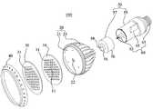
도 2는 도 1에 도시된 히트싱크의 일 예를 나타내는 도면이다.FIG. 2 is a diagram illustrating an example of the heat sink shown in FIG. 1.
히트싱크(20)는 인쇄회로기판(10) 및 회로부(60)와 각각 결합되며, 발광다이오드(11)에서 발생한 열을 발광 장치(100)의 외부로 방출한다. 히트싱크(20)는, 예를 들어, 알루미늄과 같은 열전도율이 우수하고 가벼운 금속으로 형성되는 것이 바람직하다. 히트싱크(20)는 인쇄회로기판(10)에 접촉하여 방열하는 구조를 가지며, 방열판(21), 복수의 외부 방열날개(23)들 및 복수의 내부 방열핀(25)들을 포함한다.The
방열판(21)은 대략 원판 형상을 갖는다. 방열판(21)에는, 도 1 및 도 2에 도시된 것과 같이, 회로부(60)와 발광다이오드(11)의 전기적 연결을 위해 제1 개구(22)가 형성되어 있다. 방열판(21)의 상면에는 발광다이오드(11)가 실장된 인쇄회로기판(10)이 배치된다. 인쇄회로기판(10)은 방열테이프 또는 도전성 페이스트(도시되지 않음)로 방열판(21)의 상면에 부착될 수 있다. 렌즈 플레이트(30)는 인쇄회로기판(10) 위에 배치되며, 고정부재(40)는 렌즈 플레이트(30)의 가장자리를 커버하며 방열판(21)에 결합된다.The
복수의 외부 방열날개(23)들은 방열판(21)의 하면의 가장자리로부터 발광다이오드(11)의 반대측으로 연장되어 있다. 외부 방열날개(23)들은 방사형으로 배치된다. 외부 방열날개(23)들은 방열판(21)으로부터 멀어질수록 폭이 좁아진다. 외부 방열날개(23)의 외측 에지는 방열판(21)으로부터 멀어질수록 외부 방열날개(23)의 내측 에지에 근접하도록 곡면으로 형성되어 있다. 외부 방열날개(23)는 방열판(21)의 중심을 향하는 방향에 대해 각도를 이루며 굽은 판 형상을 가질 수 있다. 따라서 방열판(21) 가장자리의 한정된 영역에서 외부 방열날개(23)의 면적을 증가시킬 수 있다.The plurality of external
본 개시에 따른 발광 장치(100)는 적어도 일부의 외부 방열날개(23)들이 서로 떨어져 있어서 외부 방열날개(23)들 사이가 개구되어(open)있다. 도 1 및 도 2에는 외부 방열날개(23)들 사이가 모두 개구된 예가 도시되어 있다. 따라서 발광 장치(100)의 히트싱크(20)는 외부 방열날개(23)들이 연결되는 중심부가 삭제되어 무게가 많이 감소된다.In the
내부 방열핀(25)들은 외부 방열날개(23) 인근의 방열판(21) 하면에서 하면의 가운데를 향하여 길게 뻗어 있다. 내부 방열핀(25)들은 방사형으로 배열되며, 하면의 가운데로부터 일정 거리 이격된 위치로부터 하면의 가장자리의 사이에 형성되어 있다. 전술된 제1 개구(22)는 내부 방열핀(25)들에 둘러진 방열판(21) 하면의 가운데에 형성되어 있다. 내부 방열핀(25)들은 방열판(21) 하면으로부터 돌출될 수도 있고, 하면에 내부 방열핀(25)들 사이에 대응하여 홈들이 형성됨에 따라 홈들을 구분하는 벽이 방열핀(25)이 될 수도 있다.The inner heat dissipation fins 25 extend from the lower surface of the
내부 방열핀(25)들이 방열판(21)과 하우징(50) 사이에 형성됨으로써 방열면적이 많이 증가하여 방열효율이 향상된다. 또한 내부 방열핀(25)들은 방열판(21)으로부터 회로부(60)로 열전달을 감소시켜 회로부(60)의 동작의 신뢰성이 향상된다.Since the internal
또한, 내부 방열핀(25)들 사이의 공간은 중심영역으로 통하는 통로가 된다. 따라서 공기는 외부 방열날개(23)들 사이의 개구 및 내부 방열핀(25)들 사이의 공간이 이루는 공기흐름 통로를 통해 방열판(21)의 가운데로 유입될 수 있고, 반대로 방열판(21)의 가운데에서 온도가 상승한 공기는 상기 공기흐름 통로를 통해 원활하게 외부로 방출될 있다. 따라서 방열효율이 향상된다.In addition, the space between the internal
도 3은 도 1에 도시된 발광 장치의 사용상태를 나타내는 도면이다. 도 4는 도 3에 도시된 발광 장치를 I-I' 선을 따라 절단한 단면도이다.3 is a view illustrating a state of use of the light emitting device illustrated in FIG. 1. 4 is a cross-sectional view of the light emitting device illustrated in FIG. 3 taken along the line II ′.
회로부(60)는 발광다이오드(11)의 발광에 필요한 전원을 공급한다. 예를 들어, 회로부(60)는 입력단(65), 회로(61) 및 커넥터(63)를 포함한다. 회로(61)는 외부로부터 전원이 인가되는 입력단(65)을 통해 전원을 인가받아 발광다이오드(11)의 구동에 필요한 전류를 공급한다. 커넥터(63)는 회로(61)와 전기적으로 연결되어 있고, 발광다이오드(11)가 실장된 인쇄회로기판(10)에 전기적으로 연결된다.The
하우징(50)은 회로부(60)를 수납하며, 히트싱크(20)에 결합된다. 하우징(50)은 몸체(55) 및 헤드(57)를 포함한다. 몸체(55) 및 헤드(57)는 절연성 물질로 이루어진 사출물일 수 있다. 몸체(55)는 통 형상을 가질 수 있고, 전방으로 개구되어 있다. 몸체(55)의 내부에는, 예를 들어, 회로부(60)가 슬롯 방식으로 설치될 수 있는 수납공간이 마련되어 있다. 몸체(55)는 내부 방열핀(25)들 아래에 위치하며, 외부 방열날개(23)들은 몸체(55)의 외측면에 위치한다. 몸체(55)는 외부 방열날개(23)들의 내측 에지에 의해 가압되도록 외부 방열날개(23)들 사이에 끼워진다.The
헤드(57)는 몸체(55)의 전단에 고정되며 몸체(55)의 전단의 개구를 커버한다. 헤드(57)는 히트싱크(20)에 결합된다. 헤드(57)는 고정부(56) 및 돌출부(58)를 포함한다.The
고정부(56)는, 예를 들어, 몸체(55)의 전단의 내측으로 가압되어 삽입된다. 따라서 고정부(56)는 내부 방열핀(25)들과 마주보며, 내부 방열핀(25)들에 접할 수 있다.The fixing
돌출부(58)는 고정부(56)의 전면(front surface)에 형성된다. 돌출부(58)는 내부 방열핀(25)들의 에지가 돌출부(58)의 외측면에 위치하도록 내부 방열핀(25)들 사이에 끼워진다. 돌출부(58)의 전면에는 방열판(21)에 형성된 제1 개구(22)에 대응하는 제2 개구(59)가 형성된다. 커넥터(63)는 제2 개구(59)로 노출될 수 있고, 제1 개구(22)에 위치하는 인쇄회로기판(10)의 접속부(15)에 접속된다.The
몸체(55)는 외부 방열날개(23)들 사이에 끼워지고 헤드(57)는 내부 방열핀(25)들 사이에 끼워진다. 따라서 하우징(50)과 히트싱크(20)가 견고한 결합한다. 도 5는 본 개시에 따른 발광 장치의 다른 예를 나타내는 도면이다. 도 6은 도 5에 도시된 히트싱크를 나타내는 도면이다. 도 7은 도 5 및 도 6에 도시된 발광 장치의 단면도이다.The
도 7에 도시된 발광 장치(300)는 히트싱크(320)의 형상 및 하우징(350)의 형상을 제외하고는 도 1 내지 도 4에서 설명된 발광 장치(100)와 실질적으로 동일하다. 따라서 대응하는 요소에 대해서는 대응하는 참조번호를 부여하고 중복된 설명은 생략한다.The
발광 장치(300)에서 방열판(321)의 하면에는 도 6에 도시된 것과 같이 제1 개구(322)의 주변에 제1 결합부(327), 예를 들어, 홈 또는 돌기가 형성된다. 헤드(357)의 돌출부(358)의 전면에는 도 5에 도시된 것과 같이 제2 결합부(354), 예를 들어 돌기 또는 홈이 형성된다. 제1 결합부(327) 및 제2 결합부(354)로 인해 헤드(357)가 히트싱크(320)에 결합이 더욱 견고하게 되며 헤드(357)의 불필요한 유격이 방지된다.In the
하우징(350)의 몸체(355)에는 도 5에 도시된 것과 같이 외측면에 결합을 위한 구조, 예를 들어, 후크(hook)(351)가 형성되어 있다. 외부 방열날개(323)들의 내측 에지에는 도 6에 도시된 것과 같이 후크(351)가 결합되는 걸림홈(324)이 형성되어 있다. 따라서 몸체(355)가 외부 방열날개(323)에 결합이 확실해 지고 하우징(350)과 히트싱크(320)의 결합이 걸림홈(324) 및 후크(351)에 맞추어 가이드 된다.The
이하, 본 개시의 다양한 실시 형태에 대하여 설명한다.Hereinafter, various embodiments of the present disclosure will be described.
(1) 헤드는 몸체의 전단에 결합하며, 내부 방열핀들 아래에 위치하는 지지부; 그리고 지지부의 전면(front surface)에 형성된 돌출부;로서, 돌출부의 외측면에 내부 방열핀들의 에지들이 위치하도록 내부 방열핀들 사이에 끼워진 돌출부;를 포함하는 것을 특징으로 하는 발광 장치.(1) the head is coupled to the front end of the body, the support is located under the inner heat radiation fins; And a protrusion formed on a front surface of the support, the protrusion being sandwiched between the internal heat dissipation fins so that the edges of the internal heat dissipation fins are positioned on the outer surface of the protrusion.
(2) 지지부의 전면은 내부 방열핀들에 접하는 것을 특징으로 하는 발광 장치.(2) The light emitting device, characterized in that the front surface of the support portion in contact with the internal heat radiation fins.
헤드는 돌출부가 없이 지지부가 직접 내부 방열핀들 사이에 끼워질 수도 있다. 이 경우, 몸체의 전단이 내부 방열핀들에 접할 수도 있다.The head may be fitted directly between the inner heat dissipation fins without the protrusions. In this case, the front end of the body may contact the internal heat dissipation fins.
(3) 방열판의 하면에는 제1 결합부가 형성되고, 돌출부의 전면(front surface)에는 제1 결합부와 결합되는 제2 결합부가 형성된 것을 특징으로 하는 발광 장치.(3) A light emitting device, characterized in that the first coupling portion is formed on the lower surface of the heat sink, and the second coupling portion is coupled to the first coupling portion on the front surface of the protrusion.
(4) 제1 결합부 및 제2 결합부는 돌기 및 돌기가 삽입되는 홈 중 서로 다르게 선택된 어느 하나인 것을 특징으로 하는 발광 장치.(4) The light emitting device, characterized in that the first engaging portion and the second engaging portion are any one selected differently from the projection and the groove into which the projection is inserted.
(5) 회로부는 몸체 내에 설치되어 외부로부터 전원을 인가받는 회로; 그리고 회로와 접속되고 제1 개구 및 제2 개구를 통하여 발광다이오드와 전기적으로 연결되는 커넥터;를 포함하는 것을 특징으로 하는 발광 장치.(5) a circuit portion installed in the body to receive power from the outside; And a connector connected to the circuit and electrically connected to the light emitting diode through the first opening and the second opening.
회로부의 커넥터와 발광다이오드가 실장된 인쇄회로기판을 전기적으로 연결하는 방법은 다양하게 변경될 수 있다. 예를 들어 커넥터는 리드전극일 수 있으며, 커넥터 대신 와이어를 사용하여 회로부와 발광다이오드가 실장된 인쇄회로기판을 전기적으로 연결할 수도 있다. 또는 인쇄회로기판에 플렉시블한 전원케이블이 연결되고 전원케이블이 회로부까지 연장되어 회로부에 연결될 수도 있다.The method of electrically connecting the connector of the circuit unit and the printed circuit board on which the light emitting diodes are mounted may be variously changed. For example, the connector may be a lead electrode, and a wire may be used instead of the connector to electrically connect the circuit unit and the printed circuit board on which the light emitting diodes are mounted. Alternatively, a flexible power cable may be connected to the printed circuit board, and the power cable may extend to the circuit portion to be connected to the circuit portion.
(6) 외부 방열날개들은 방열판으로부터 멀어질수록 폭이 좁아지는 것을 특징으로 하는 발광 장치.(6) The light emitting device characterized in that the outer heat dissipation wings become narrower as they move away from the heat dissipation plate.
(7) 외부 방열날개들은 굴곡된 형상을 갖는 것을 특징으로 하는 발광 장치.(7) A light emitting device characterized in that the outer heat dissipation wings have a curved shape.
외부 방열날개들 사이는 모두 개구되거나 폐쇄된 것과 개구된 것이 교대로 형성될 수 있다.Between the outer heat dissipation blades, all of which are open or closed and which are open may be alternately formed.
(8) 몸체의 외측면에는 후크가 형성되고, 적어도 하나의 외부 방열날개에는 내측 에지에 후크가 결합되는 홈이 형성된 것을 특징으로 하는 발광 장치.(8) The light emitting device, characterized in that the hook is formed on the outer surface of the body, the groove is coupled to the inner edge of the at least one outer heat dissipation wing.
(9) 외부 방열날개들 및 내부 방열핀들은 방사형으로 배치되며, 방열날개들 사이의 개구와 방열핀들 사이 개구는 공기 흐름의 통로를 형성하는 것을 특징으로 하는 발광 장치.(9) The light emitting device characterized in that the outer heat dissipation blades and the inner heat dissipation fins are radially disposed, and the opening between the heat dissipation wings and the opening between the heat dissipation fins form a passage of air flow.
본 개시에 따른 하나의 발광 장치에 의하면, 내부 방열핀들 사이에 헤드가 끼워짐에 따라 히트싱크와 하우징의 결합이 견고하게 되어 발광 장치의 신뢰성이 향상된다.According to one light emitting device according to the present disclosure, as the head is sandwiched between the internal heat dissipation fins, the coupling of the heat sink and the housing is firm, thereby improving the reliability of the light emitting device.
또한, 본 개시에 따른 다른 하나의 발광 장치에 의하면, 내부 방열핀으로 인해 방열면적이 증가하여 방열효율이 향상된다.In addition, according to another light emitting device according to the present disclosure, the heat radiation area is increased due to the internal heat radiation fins, thereby improving heat radiation efficiency.
또한, 본 개시에 따른 또 다른 하나의 발광 장치에 의하면, 외부 방열날개들 사이가 개구되어 발광 장치의 무게가 감소하며, 외부 방열날개들 사이의 개구 및 내부 방열핀들 사이 공간이 공기흐름 통로를 형성하여 방열효율이 향상된다.In addition, according to another light emitting device according to the present disclosure, the weight of the light emitting device is reduced by opening between the external heat dissipation wings, and the space between the openings between the external heat dissipation wings and the internal heat dissipation fins forms an airflow passage. Thus, heat dissipation efficiency is improved.
10 : 인쇄회로기판11 : 발광다이오드
20 : 히트싱크21 : 방열판
22 : 제1 개구23 : 외부 방열날개
25 : 내부 방열핀30 : 렌즈 플레이트
40 : 고정부재50 : 하우징
55 : 몸체56 : 고정부
57 : 헤드58 : 돌출부
59 : 제2 개구60 : 회로부
61 : 회로63 : 커넥터
100 : 발광 장치
10: printed circuit board 11: light emitting diode
20: heat sink 21: heat sink
22: first opening 23: external heat dissipation wing
25: internal heat radiation fin 30: lens plate
40: fixing member 50: housing
55
57: head 58: protrusion
59: second opening 60: circuit portion
61
100: light emitting device
Claims (10)
Translated fromKorean발광다이오드가 위치하는 상면과, 상면과 대향하는 하면을 갖는 방열판;
방열판의 하면의 가장자리에서 발광다이오드의 반대측으로 연장된 복수의 외부 방열날개들;로서, 적어도 일부의 외부 방열날개들은 서로 떨어져 있어서 외부 방열날개들 사이가 개구된 복수의 외부 방열날개들;
외부 방열날개들 인근 하면에서 하면의 가운데를 향하여 뻗은 복수의 내부 방열핀들;
발광다이오드가 빛을 내기 위한 전원을 공급하는 회로부; 그리고,
회로부를 수납하는 하우징;으로서, 외측면에 외부 방열날개들이 위치하도록 외부 방열날개들 사이에 위치하는 몸체와, 몸체와 방열판 사이에 위치하며 외측면에 내부 방열핀들의 에지들이 위치하도록 내부 방열핀들 사이에 끼워진 헤드를 갖는 하우징;을 포함하며,
헤드는 몸체의 전단에 결합하며 몸체와 내부 방열핀들 사이에 위치하는 지지부와, 지지부의 전면(front surface)에 형성된 돌출부를 포함하며, 돌출부의 외측면에 내부 방열핀들의 에지들이 위치하도록 돌출부가 내부 방열핀들 사이에 끼워진 것을 특징으로 하는 발광 장치.Light emitting diodes;
A heat sink having a top surface on which the light emitting diodes are positioned and a bottom surface opposite to the top surface;
A plurality of external heat dissipation blades extending from an edge of the bottom surface of the heat sink to the opposite side of the light emitting diode, wherein at least some of the external heat dissipation wings are spaced apart from each other so that the plurality of external heat dissipation wings are opened between the external heat dissipation wings;
A plurality of internal heat dissipation fins extending from the lower surface of the lower heat dissipation surface toward the center of the lower surface;
A circuit unit for supplying power for emitting light from the light emitting diode; And,
A housing for accommodating the circuit portion, comprising: a body positioned between the outer heat dissipation wings so that the outer heat dissipation wings are located on the outer side, and between the body and the heat dissipation plate, and between the inner heat dissipation fins so that the edges of the inner heat dissipation fins are located on the outer side. A housing having a fitted head;
The head is coupled to the front end of the body and includes a support positioned between the body and the internal heat dissipation fins, and a protrusion formed on the front surface of the support, and the internal heat dissipation fin so that the edges of the internal heat dissipation fins are located on the outer surface of the protrusion. Light-emitting device, characterized in that sandwiched between the.
지지부의 전면은 내부 방열핀들에 접하는 것을 특징으로 하는 발광 장치.The method according to claim 1,
Light emitting device, characterized in that the front surface of the support portion in contact with the internal heat radiation fins.
방열판의 하면에는 제1 결합부가 형성되고, 돌출부의 전면(front surface)에는 제1 결합부와 결합되는 제2 결합부가 형성된 것을 특징으로 하는 발광 장치.The method according to claim 1,
A first coupling portion is formed on the bottom surface of the heat sink, and a second coupling portion coupled to the first coupling portion is formed on the front surface of the protrusion.
제1 결합부 및 제2 결합부는 돌기 및 돌기가 삽입되는 홈 중 서로 다르게 선택된 어느 하나인 것을 특징으로 하는 발광 장치.The method of claim 4,
The light emitting device of claim 1, wherein the first coupling part and the second coupling part are ones selected differently from the projections and the grooves into which the projections are inserted.
회로부는
몸체 내에 설치되어 외부로부터 전원을 인가받는 회로; 그리고
회로와 접속되고 발광다이오드와 전기적으로 연결되는 커넥터;를 포함하는 것을 특징으로 하는 발광 장치.The method according to claim 1,
Circuit part
A circuit installed in the body to receive power from the outside; And
And a connector connected to the circuit and electrically connected to the light emitting diode.
외부 방열날개들은 방열판으로부터 멀어질수록 폭이 좁아지는 것을 특징으로 하는 발광 장치.The method according to claim 1,
The outer heat dissipation wings are lighter device characterized in that the width becomes narrower away from the heat sink.
외부 방열날개들은 굴곡된 형상을 갖는 것을 특징으로 하는 발광 장치.The method of claim 7,
The external heat dissipation wings have a curved shape.
몸체의 외측면에는 후크가 형성되고, 적어도 하나의 외부 방열날개에는 내측 에지에 후크가 결합되는 홈이 형성된 것을 특징으로 하는 발광 장치.The method of claim 7,
A hook is formed on an outer surface of the body, and the light emitting device, characterized in that the at least one outer heat dissipation wing is formed with a groove coupled to the inner edge.
외부 방열날개들 및 내부 방열핀들은 방사형으로 배치되며, 방열날개들 사이의 개구와 방열핀들 사이 개구는 공기 흐름의 통로를 형성하는 것을 특징으로 하는 발광 장치.
The method according to claim 1,
The outer heat dissipation wings and the inner heat dissipation fins are radially disposed, and the opening between the heat dissipation wings and the opening between the heat dissipation fins form a passage of air flow.
Priority Applications (1)
| Application Number | Priority Date | Filing Date | Title |
|---|---|---|---|
| KR1020100093561AKR101175754B1 (en) | 2010-09-28 | 2010-09-28 | Light emitting device |
Applications Claiming Priority (1)
| Application Number | Priority Date | Filing Date | Title |
|---|---|---|---|
| KR1020100093561AKR101175754B1 (en) | 2010-09-28 | 2010-09-28 | Light emitting device |
Publications (2)
| Publication Number | Publication Date |
|---|---|
| KR20120032115A KR20120032115A (en) | 2012-04-05 |
| KR101175754B1true KR101175754B1 (en) | 2012-08-21 |
Family
ID=46135300
Family Applications (1)
| Application Number | Title | Priority Date | Filing Date |
|---|---|---|---|
| KR1020100093561AExpired - Fee RelatedKR101175754B1 (en) | 2010-09-28 | 2010-09-28 | Light emitting device |
Country Status (1)
| Country | Link |
|---|---|
| KR (1) | KR101175754B1 (en) |
Families Citing this family (2)
| Publication number | Priority date | Publication date | Assignee | Title |
|---|---|---|---|---|
| KR101466734B1 (en)* | 2012-08-14 | 2014-12-01 | 한양대학교 산학협력단 | Heatsink used in lighting device |
| CN118472727A (en)* | 2024-04-30 | 2024-08-09 | 东莞市思普太阳能科技有限公司 | New energy charging adapter |
- 2010
- 2010-09-28KRKR1020100093561Apatent/KR101175754B1/ennot_activeExpired - Fee Related
Also Published As
| Publication number | Publication date |
|---|---|
| KR20120032115A (en) | 2012-04-05 |
Similar Documents
| Publication | Publication Date | Title |
|---|---|---|
| JP5101578B2 (en) | Light emitting diode lighting device | |
| EP2541140B1 (en) | Lighting device | |
| CN101785117B (en) | lighting device | |
| EP2400214B1 (en) | Lighting device | |
| US20110109215A1 (en) | Lighting device | |
| EP2295854A1 (en) | Heat Dissipating Device for Lighting Devices | |
| US9453617B2 (en) | LED light device with improved thermal and optical characteristics | |
| JP5197659B2 (en) | Lighting device | |
| JP2004095655A (en) | LED device and LED lighting device | |
| JP5500971B2 (en) | Light source module and lighting device | |
| KR20100087964A (en) | High power light emitting diode lamp | |
| KR101175754B1 (en) | Light emitting device | |
| KR102148846B1 (en) | PRINTED CIRCUIT BOARD AND luminous device INCLUDING THE SAME | |
| KR20190053399A (en) | Led light apparatus | |
| KR101876948B1 (en) | Illuminating lamp | |
| KR100646638B1 (en) | Light emitting diode lighting device and manufacturing method | |
| CN212252178U (en) | Bulb | |
| KR20120017642A (en) | Light emitting device | |
| KR101744114B1 (en) | LED lighting device) | |
| KR101580789B1 (en) | Lighting device | |
| KR101617296B1 (en) | Lighting device | |
| KR20150012555A (en) | Led lamp | |
| KR101977649B1 (en) | Lighting device | |
| KR101288910B1 (en) | Lighting device | |
| JP2015046303A (en) | Lamp |
Legal Events
| Date | Code | Title | Description |
|---|---|---|---|
| A201 | Request for examination | ||
| PA0109 | Patent application | St.27 status event code:A-0-1-A10-A12-nap-PA0109 | |
| PA0201 | Request for examination | St.27 status event code:A-1-2-D10-D11-exm-PA0201 | |
| E902 | Notification of reason for refusal | ||
| PE0902 | Notice of grounds for rejection | St.27 status event code:A-1-2-D10-D21-exm-PE0902 | |
| E13-X000 | Pre-grant limitation requested | St.27 status event code:A-2-3-E10-E13-lim-X000 | |
| P11-X000 | Amendment of application requested | St.27 status event code:A-2-2-P10-P11-nap-X000 | |
| P13-X000 | Application amended | St.27 status event code:A-2-2-P10-P13-nap-X000 | |
| PG1501 | Laying open of application | St.27 status event code:A-1-1-Q10-Q12-nap-PG1501 | |
| E701 | Decision to grant or registration of patent right | ||
| PE0701 | Decision of registration | St.27 status event code:A-1-2-D10-D22-exm-PE0701 | |
| GRNT | Written decision to grant | ||
| PR0701 | Registration of establishment | St.27 status event code:A-2-4-F10-F11-exm-PR0701 | |
| PR1002 | Payment of registration fee | Fee payment year number:1 St.27 status event code:A-2-2-U10-U11-oth-PR1002 | |
| PG1601 | Publication of registration | St.27 status event code:A-4-4-Q10-Q13-nap-PG1601 | |
| PN2301 | Change of applicant | St.27 status event code:A-5-5-R10-R11-asn-PN2301 St.27 status event code:A-5-5-R10-R13-asn-PN2301 | |
| R18-X000 | Changes to party contact information recorded | St.27 status event code:A-5-5-R10-R18-oth-X000 | |
| FPAY | Annual fee payment | Payment date:20150717 Year of fee payment:4 | |
| PR1001 | Payment of annual fee | Fee payment year number:4 St.27 status event code:A-4-4-U10-U11-oth-PR1001 | |
| P22-X000 | Classification modified | St.27 status event code:A-4-4-P10-P22-nap-X000 | |
| FPAY | Annual fee payment | Payment date:20160812 Year of fee payment:5 | |
| PR1001 | Payment of annual fee | Fee payment year number:5 St.27 status event code:A-4-4-U10-U11-oth-PR1001 | |
| P22-X000 | Classification modified | St.27 status event code:A-4-4-P10-P22-nap-X000 | |
| LAPS | Lapse due to unpaid annual fee | ||
| PC1903 | Unpaid annual fee | Not in force date:20170815 Payment event data comment text:Termination Category : DEFAULT_OF_REGISTRATION_FEE St.27 status event code:A-4-4-U10-U13-oth-PC1903 | |
| P22-X000 | Classification modified | St.27 status event code:A-4-4-P10-P22-nap-X000 | |
| PC1903 | Unpaid annual fee | Ip right cessation event data comment text:Termination Category : DEFAULT_OF_REGISTRATION_FEE Not in force date:20170815 St.27 status event code:N-4-6-H10-H13-oth-PC1903 | |
| P22-X000 | Classification modified | St.27 status event code:A-4-4-P10-P22-nap-X000 | |
| P22-X000 | Classification modified | St.27 status event code:A-4-4-P10-P22-nap-X000 | |
| P22-X000 | Classification modified | St.27 status event code:A-4-4-P10-P22-nap-X000 | |
| P22-X000 | Classification modified | St.27 status event code:A-4-4-P10-P22-nap-X000 | |
| PN2301 | Change of applicant | St.27 status event code:A-5-5-R10-R11-asn-PN2301 St.27 status event code:A-5-5-R10-R13-asn-PN2301 | |
| R18-X000 | Changes to party contact information recorded | St.27 status event code:A-5-5-R10-R18-oth-X000 |