KR101173344B1 - Solar cell and mehtod of fabricating the same - Google Patents
Solar cell and mehtod of fabricating the sameDownload PDFInfo
- Publication number
- KR101173344B1 KR101173344B1KR1020090104468AKR20090104468AKR101173344B1KR 101173344 B1KR101173344 B1KR 101173344B1KR 1020090104468 AKR1020090104468 AKR 1020090104468AKR 20090104468 AKR20090104468 AKR 20090104468AKR 101173344 B1KR101173344 B1KR 101173344B1
- Authority
- KR
- South Korea
- Prior art keywords
- layer
- light absorbing
- absorbing layer
- substrate
- hole
- Prior art date
- Legal status (The legal status is an assumption and is not a legal conclusion. Google has not performed a legal analysis and makes no representation as to the accuracy of the status listed.)
- Expired - Fee Related
Links
Images


Classifications
- H—ELECTRICITY
- H10—SEMICONDUCTOR DEVICES; ELECTRIC SOLID-STATE DEVICES NOT OTHERWISE PROVIDED FOR
- H10F—INORGANIC SEMICONDUCTOR DEVICES SENSITIVE TO INFRARED RADIATION, LIGHT, ELECTROMAGNETIC RADIATION OF SHORTER WAVELENGTH OR CORPUSCULAR RADIATION
- H10F19/00—Integrated devices, or assemblies of multiple devices, comprising at least one photovoltaic cell covered by group H10F10/00, e.g. photovoltaic modules
- H10F19/30—Integrated devices, or assemblies of multiple devices, comprising at least one photovoltaic cell covered by group H10F10/00, e.g. photovoltaic modules comprising thin-film photovoltaic cells
- H—ELECTRICITY
- H10—SEMICONDUCTOR DEVICES; ELECTRIC SOLID-STATE DEVICES NOT OTHERWISE PROVIDED FOR
- H10F—INORGANIC SEMICONDUCTOR DEVICES SENSITIVE TO INFRARED RADIATION, LIGHT, ELECTROMAGNETIC RADIATION OF SHORTER WAVELENGTH OR CORPUSCULAR RADIATION
- H10F77/00—Constructional details of devices covered by this subclass
- H10F77/10—Semiconductor bodies
- H10F77/16—Material structures, e.g. crystalline structures, film structures or crystal plane orientations
- H10F77/169—Thin semiconductor films on metallic or insulating substrates
- H10F77/1698—Thin semiconductor films on metallic or insulating substrates the metallic or insulating substrates being flexible
- H10F77/1699—Thin semiconductor films on metallic or insulating substrates the metallic or insulating substrates being flexible the films including Group I-III-VI materials, e.g. CIS or CIGS on metal foils or polymer foils
- H—ELECTRICITY
- H10—SEMICONDUCTOR DEVICES; ELECTRIC SOLID-STATE DEVICES NOT OTHERWISE PROVIDED FOR
- H10F—INORGANIC SEMICONDUCTOR DEVICES SENSITIVE TO INFRARED RADIATION, LIGHT, ELECTROMAGNETIC RADIATION OF SHORTER WAVELENGTH OR CORPUSCULAR RADIATION
- H10F19/00—Integrated devices, or assemblies of multiple devices, comprising at least one photovoltaic cell covered by group H10F10/00, e.g. photovoltaic modules
- H10F19/30—Integrated devices, or assemblies of multiple devices, comprising at least one photovoltaic cell covered by group H10F10/00, e.g. photovoltaic modules comprising thin-film photovoltaic cells
- H10F19/31—Integrated devices, or assemblies of multiple devices, comprising at least one photovoltaic cell covered by group H10F10/00, e.g. photovoltaic modules comprising thin-film photovoltaic cells having multiple laterally adjacent thin-film photovoltaic cells deposited on the same substrate
- H—ELECTRICITY
- H10—SEMICONDUCTOR DEVICES; ELECTRIC SOLID-STATE DEVICES NOT OTHERWISE PROVIDED FOR
- H10F—INORGANIC SEMICONDUCTOR DEVICES SENSITIVE TO INFRARED RADIATION, LIGHT, ELECTROMAGNETIC RADIATION OF SHORTER WAVELENGTH OR CORPUSCULAR RADIATION
- H10F77/00—Constructional details of devices covered by this subclass
- H10F77/10—Semiconductor bodies
- H10F77/16—Material structures, e.g. crystalline structures, film structures or crystal plane orientations
- H10F77/169—Thin semiconductor films on metallic or insulating substrates
- H10F77/1694—Thin semiconductor films on metallic or insulating substrates the films including Group I-III-VI materials, e.g. CIS or CIGS
- Y—GENERAL TAGGING OF NEW TECHNOLOGICAL DEVELOPMENTS; GENERAL TAGGING OF CROSS-SECTIONAL TECHNOLOGIES SPANNING OVER SEVERAL SECTIONS OF THE IPC; TECHNICAL SUBJECTS COVERED BY FORMER USPC CROSS-REFERENCE ART COLLECTIONS [XRACs] AND DIGESTS
- Y02—TECHNOLOGIES OR APPLICATIONS FOR MITIGATION OR ADAPTATION AGAINST CLIMATE CHANGE
- Y02E—REDUCTION OF GREENHOUSE GAS [GHG] EMISSIONS, RELATED TO ENERGY GENERATION, TRANSMISSION OR DISTRIBUTION
- Y02E10/00—Energy generation through renewable energy sources
- Y02E10/50—Photovoltaic [PV] energy
- Y02E10/541—CuInSe2 material PV cells
- Y—GENERAL TAGGING OF NEW TECHNOLOGICAL DEVELOPMENTS; GENERAL TAGGING OF CROSS-SECTIONAL TECHNOLOGIES SPANNING OVER SEVERAL SECTIONS OF THE IPC; TECHNICAL SUBJECTS COVERED BY FORMER USPC CROSS-REFERENCE ART COLLECTIONS [XRACs] AND DIGESTS
- Y02—TECHNOLOGIES OR APPLICATIONS FOR MITIGATION OR ADAPTATION AGAINST CLIMATE CHANGE
- Y02P—CLIMATE CHANGE MITIGATION TECHNOLOGIES IN THE PRODUCTION OR PROCESSING OF GOODS
- Y02P70/00—Climate change mitigation technologies in the production process for final industrial or consumer products
- Y02P70/50—Manufacturing or production processes characterised by the final manufactured product
Landscapes
- Photovoltaic Devices (AREA)
- Life Sciences & Earth Sciences (AREA)
- Sustainable Development (AREA)
Abstract
Translated fromKoreanDescription
Translated fromKorean실시예는 태양전지 및 이의 제조방법에 관한 것이다.An embodiment relates to a solar cell and a manufacturing method thereof.
최근 에너지의 수요가 증가함에 따라서, 태양광 에너지를 전기에너지로 변환시키는 태양전지들에 대한 개발이 진행되고 있다.Recently, as the demand for energy increases, development of solar cells for converting solar energy into electrical energy is in progress.
특히, 유리 기판, 금속 후면 전극층, p형 CIGS계 광 흡수층, 버퍼층, n형 창층 등을 포함하는 기판 구조의 pn 헤테로 접합 장치인 CIGS계 태양전지가 사용되고 있다.In particular, CIGS-based solar cells, which are pn heterojunction devices of a substrate structure, including a glass substrate, a metal back electrode layer, a p-type CIGS-based light absorbing layer, a buffer layer, an n-type window layer, and the like are used.
상기 후면전극층과 n형 창층은 상기 광 흡수층 및 버퍼층에 형성된 관통홀을 통해 연결될 수 있다The back electrode layer and the n-type window layer may be connected through through holes formed in the light absorbing layer and the buffer layer.
상기 관통홀은 기계적 또는 레이저를 이용한 패터닝 공정에 의하여 형성되므로 파티클 등이 남아있을 수 있게 되어, 태양전지 셀의 직렬저항 및 누설전류를 발생의 요인이 될 수 있다.Since the through hole is formed by a mechanical or laser patterning process, particles and the like may remain, which may cause a series resistance and leakage current of the solar cell.
또한, 상기 광 흡수층은 고온에서 형성되므로, 고온 공정을 견딜 수 있는 강성의 기판을 사용하게 된다. 따라서, 기판 사용에 제약이 따를 수 있다.In addition, since the light absorbing layer is formed at a high temperature, a rigid substrate capable of withstanding a high temperature process is used. Thus, there may be restrictions on the use of the substrate.
실시예에서는 전기적 특성을 향상시킬 수 있는 태양전지 및 이의 제조방법을 제공한다.The embodiment provides a solar cell and a method of manufacturing the same that can improve electrical characteristics.
실시예에 따른 태양전지는, 기판 상에 형성되고 제1 관통홀에 의하여 분리된 후면전극; 상기 제1 관통홀을 포함하는 상기 후면전극 상에 형성된 광 흡수층; 상기 광 흡수층을 관통하여 상기 후면전극을 노출시키는 제2 관통홀; 상기 광 흡수층의 표면에 형성된 버퍼층; 상기 버퍼층 상에 형성된 전면전극층; 및 상기 전면전극층에서 연장되어 상기 제2 관통홀 내부에 형성된 접속배선을 포함한다.A solar cell according to an embodiment includes a back electrode formed on a substrate and separated by a first through hole; A light absorbing layer formed on the back electrode including the first through hole; A second through hole penetrating the light absorbing layer to expose the back electrode; A buffer layer formed on the surface of the light absorbing layer; A front electrode layer formed on the buffer layer; And a connection wiring extending from the front electrode layer and formed in the second through hole.
실시예에 따른 태양전지의 제조방법은, 지지기판 상에 후면전극층을 형성하고, 상기 후면전극층이 상호 분리되도록 제1 관통홀을 단계; 캐리어 기판 상에 광 흡수층을 형성하는 단계; 상기 제1 관통홀과 인접하는 위치를 가지도록 상기 광 흡수층을 관통하는 제2 관통홀을 형성하는 단계; 상기 지지기판과 상기 캐리어 기판을 본딩하여, 상기 후면전극층 상에 상기 광 흡수층을 형성하는 단계; 상기 캐리어 기판을 제거하고, 상기 광 흡수층을 노출시키는 단계; 상기 광 흡수층의 표면에 버퍼층을 형성하는 단계; 상기 버퍼층 상에 전면전극층을 형성하고, 상기 제2 관통홀의 내부에는 접속배선을 형성하는 단계를 포함한다.In accordance with another aspect of the present invention, there is provided a method of manufacturing a solar cell, the method comprising: forming a rear electrode layer on a support substrate, and forming a first through hole to separate the rear electrode layer from each other; Forming a light absorbing layer on the carrier substrate; Forming a second through hole penetrating the light absorbing layer to have a position adjacent to the first through hole; Bonding the support substrate and the carrier substrate to form the light absorbing layer on the back electrode layer; Removing the carrier substrate and exposing the light absorbing layer; Forming a buffer layer on a surface of the light absorbing layer; Forming a front electrode layer on the buffer layer, and forming a connection wiring in the second through hole.
실시예에 의하면, 태양전지의 전기적 특성을 향상시킬 수 있다.According to the embodiment, the electrical characteristics of the solar cell can be improved.
특히, 광기전력을 발생시키는 CIGS 광 흡수층이 셀별로 패터닝 되고, 상기 광 흡수층의 노출된 표면에 버퍼층이 형성되어 있으므로, 리키지 커런트를 방지할 수 있다.In particular, since the CIGS light absorbing layer generating photovoltaic power is patterned for each cell, and a buffer layer is formed on the exposed surface of the light absorbing layer, it is possible to prevent leakage current.
또한, 상기 광 흡수층과 버퍼층의 접합면적 확장에 따라, 광전하 발생률을 향상시킬 수 있다.In addition, as the junction area between the light absorbing layer and the buffer layer is extended, the photocharge generation rate may be improved.
또한, 상기 광 흡수층은 캐리어 기판에 별도로 형성한 후, 후면전극층이 형성된 지지기판과 본딩될 수 있다.In addition, the light absorbing layer may be separately formed on the carrier substrate and then bonded to the support substrate on which the rear electrode layer is formed.
이에 따라, 상기 지지기판은 다양한 기판, 즉, 하드 또는 플렉서블한 기판의 사용이 가능하다. 또한, 상기 기판은 슬림화, 경량화될 수 있으므로 다양한 영역에 적용될 수 있다.Accordingly, the support substrate may use a variety of substrates, that is, a hard or flexible substrate. In addition, since the substrate can be slimmed and lightweight, it can be applied to various areas.
또한, 상기 광 흡수층은 캐리어 기판 상에 형성되고, 고온공정이 가능하므로, 상기 광 흡수층의 결정화도를 높일 수 있다.In addition, since the light absorbing layer is formed on the carrier substrate and a high temperature process is possible, the degree of crystallinity of the light absorbing layer can be increased.
이에 따라, 상기 광 흡수층의 전기적 특성을 향상시킬 수 있다.Accordingly, the electrical characteristics of the light absorbing layer can be improved.
실시예에 따른 태양전지는 다양한 기판, 즉 하드 또는 플렉서블한 기판의 적용이 가능하다.The solar cell according to the embodiment may be applied to various substrates, that is, hard or flexible substrates.
실시 예의 설명에 있어서, 각 기판, 층, 막, 결정 또는 전극 등이 각 기판, 층, 막, 결정 또는 전극 등의 "상(on)"에 또는 "아래(under)"에 형성되는 것으로 기재되는 경우에 있어, "상(on)"과 "아래(under)"는 "직접(directly)" 또는 "다른 구성요소를 개재하여 (indirectly)" 형성되는 것을 모두 포함한다. 또한 각 구성요 소의 상 또는 아래에 대한 기준은 도면을 기준으로 설명한다. 도면에서의 각 구성요소들의 크기는 설명을 위하여 과장될 수 있으며, 실제로 적용되는 크기를 의미하는 것은 아니다.In the description of the embodiments, each substrate, layer, film, crystal, or electrode is described as being formed "on" or "under" of each substrate, layer, film, crystal, or electrode. In the case, “on” and “under” include both being formed “directly” or “indirectly” through other components. In addition, the criteria for the top or bottom of each component will be described based on the drawings. The size of each component in the drawings may be exaggerated for the sake of explanation and does not mean the size actually applied.
도 1 내지 도 10은 실시예에 따른 태양전지의 제조방법을 도시한 단면도이다.1 to 10 are cross-sectional views illustrating a method of manufacturing a solar cell according to an embodiment.
도 1을 참조하여, 지지기판(100) 상에 후면전극층(200) 및 전도성 접착층(300)이 형성된다.Referring to FIG. 1, a
상기 지지기판(100)은 유리(glass)가 사용될 수 있으며, 세라믹 기판, 금속기판 또는 폴리머 기판 등도 사용될 수 있다.The
예를 들어, 유리 기판으로는 소다라임 유리(sodalime glass) 또는 고변형점 소다유리(high strained point soda glass)를 사용할 수 있다. 금속 기판으로는 스테인레스 스틸 또는 티타늄을 포함하는 기판을 사용할 수 있다 폴리머 기판으로는 폴리이미드(polyimide)를 사용할 수 있다.For example, soda lime glass or high strained point soda glass may be used as the glass substrate. As the metal substrate, a substrate including stainless steel or titanium may be used. As the polymer substrate, polyimide may be used.
상기 지지기판(100)은 투명할 수 있다. 상기 지지기판(100)은 리지드(rigid)하거나 플렉서블(flexible) 할 수 있다.The supporting
특히, 실시예에서는 상기 지지기판(100)은 플렉서블한 연성 기판을 사용할 수 있다. 예를 들어, 상기 지지기판(100)은 플라스틱과 같은 폴리머 계열 및 스테인레스(SUS) 계열의 플렉서블 기판이 사용될 수 있다.In particular, in the embodiment, the
상기 후면전극층(200)은 금속 등의 도전체로 형성될 수 있다.The
예를 들어, 상기 후면전극층(200)은 몰리브덴(Mo)을 타겟으로 사용하여, 스 퍼터링(sputtering) 공정에 의해 형성될 수 있다.For example, the
이는, 몰리브덴(Mo)이 가진 높은 전기전도도, 광 흡수층과의 오믹(ohmic) 접합, Se 분위기 하에서의 고온 안정성 때문이다.This is because of high electrical conductivity of molybdenum (Mo), ohmic bonding with the light absorbing layer, and high temperature stability under Se atmosphere.
상기 후면전극층(200)인 몰리브덴(Mo) 박막은 전극으로서 비저항이 낮아야하고, 열팽창 계수의 차이로 인하여 박리현상이 일어나지 않도록 기판(100)에의 점착성이 뛰어나야 한다.The molybdenum (Mo) thin film, which is the
한편, 상기 후면전극층(200)을 형성하는 물질은 이에 한정되지 않고, 나트륨(Na) 이온이 도핑된 몰리브덴(Mo)으로 형성될 수도 있다.Meanwhile, the material forming the
도면에 도시되지는 않았지만, 상기 후면전극층(200)은 적어도 하나 이상의 층으로 형성될 수 있다. 상기 후면전극층(200)이 복수개의 층으로 형성될 때, 상기 후면전극층(200)을 이루는 층들은 서로 다른 물질로 형성될 수 있다.Although not shown in the drawing, the
상기 후면전극층(200) 상에 전도성 접착층(300)이 형성된다.A conductive
상기 전도성 접착층(300)은 전도성 접착제일 수 있다.The conductive
예를 들어, 상기 전도성 접착층(300)은 카본, 알루미늄 또는 텅스텐과 같은 금속, 수지 및 플릿(frit)이 혼합되어 있는 접착성 물질일 수 있다.For example, the conductive
상기 전도성 접착층(300)의 저항률은 1×10⁻⁵~10×10-5 로서 상기 후면전극층(200)과 전기적으로 연결될 수 있다.The resistivity of the conductive
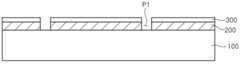
도 2를 참조하여, 상기 후면전극층(200) 및 전도성 접착층(300)을 관통하는 제1 관통홀(P1)이 형성된다. 상기 제1 관통홀(P1)은 상기 지지기판(100)의 상면을 노출시킬 수 있다.Referring to FIG. 2, a first through hole P1 penetrating the
상기 제1 관통홀(P1)에 의하여 상기 후면전극층(200) 및 전도성 접착층(300)은 다수개로 분리될 수 있다.The
상기 제1 관통홀(P1)에 의하여 상기 후면전극층(200) 및 전도성 접착층(300)은 스트라이프(stripe) 형태 또는 매트릭스(matrix) 형태로 배치될 수 있으며, 각각의 셀에 대응할 수 있다.The
한편, 상기 후면전극층(200)은 상기의 형태에 한정되지 않고 다양한 형태로 형성될 수 있다.On the other hand, the
도 3을 참조하여, 캐리어 기판(110) 상에 서브 전극층(210) 및 광 흡수층(400)이 형성된다.Referring to FIG. 3, the
상기 캐리어 기판(110)은 유리(glass)가 사용될 수 있으며, 세라믹 기판, 금속기판 또는 폴리머 기판 등도 사용될 수 있다.Glass may be used as the
상기 캐리어 기판(100)은 리지드(rigid)한 강성의 기판을 사용할 수 있다.The
예를 들어, 상기 캐리어 기판(110)은 소다라임 글래스, 넌-알칼리 글래스 및 로우-알칼리 글래스가 사용될 수 있다.For example, the
상기 캐리어 기판(110)은 상기 지지기판(100)에 비하여 상대적으로 두꺼운 두께로 형성될 수 있다.The
예를 들어, 상기 지지기판(100)과 캐리어 기판(110)은 1:3~10의 두께를 가지도록 형성될 수 있다.For example, the
이는 상기 광 흡수층(400)이 고온에서 형성되기 때문에 상기 캐리어 기판(110)은 고온공정을 견딜 수 있도록 충분히 두꺼운 두께 및 단단한 성질을 가져 야만 하기 때문이다.This is because since the
상기 캐리어 기판(110) 상에 상기 서브 전극층(210)이 형성된다. 상기 서브 전극층(210)은 금속 등의 도전체로 형성될 수 있다.The
상기 서브 전극층(210)은 열팽창 계수의 차이로 인하여 박리현상이 일어나지 않도록 상기 캐리어 기판(110)과의 점착성이 뛰어나야 한다.The
예를 들어, 상기 서브 전극층(210)은 몰리브덴(Mo)을 타겟으로 사용하여, 스퍼터링(sputtering) 공정에 의해 형성될 수 있다.For example, the
한편, 상기 서브 전극층(210)은 형성되지 않을 수도 있다.Meanwhile, the
상기 서브 전극층(210) 상에 광 흡수층(400)이 형성된다.The light absorbing
상기 광 흡수층(400)은 Ⅰb-Ⅲb-Ⅵb계 화합물을 포함한다The light absorbing
더 자세하게, 상기 광 흡수층(400)은 구리-인듐-갈륨-셀레나이드계(Cu(In, Ga)Se2, CIGS계) 화합물을 포함한다.In more detail, the
이와는 다르게, 상기 광 흡수층(400)은 구리-인듐-셀레나이드계(CuInSe2, CIS계) 화합물 또는 구리-갈륨-셀레나이드계(CuGaSe2, CGS계) 화합물을 포함할 수 있다.Alternatively, the
예를 들어, 상기 광 흡수층(400)을 형성하기 위해서, 구리 타겟, 인듐 타겟 및 갈륨 타겟을 사용하여, 상기 서브 전극층(210) 상에 CIG계 금속 프리커서(precursor)막이 형성된다.For example, in order to form the
이후, 상기 금속 프리커서막은 셀레니제이션(selenization) 공정에 의해서, 셀레늄(Se)과 반응하여 CIGS계 광 흡수층(400)이 형성된다.Thereafter, the metal precursor film is reacted with selenium (Se) by a selenization process to form a CIGS-based
또한, 상기 광 흡수층(400)은 구리,인듐,갈륨,셀레나이드(Cu, In, Ga, Se)를 동시증착법(co-evaporation)에 의해 형성할 수도 있다.In addition, the
상기 광 흡수층(400)은 외부의 광을 입사받아, 전기 에너지로 변환시킨다. 상기 광 흡수층(400)은 광전효과에 의해서 광 기전력을 생성한다.The light
상기 광 흡수층(400)은 1000℃ 이상의 고온에서 형성되므로, CIGS 화합물의 결정화도가 향상될 수 있다.Since the
도 4를 참조하여, 상기 광 흡수층(400)을 관통하는 제2 관통홀(P2)이 형성된다. 상기 제2 관통홀(P2)은 상기 서브 전극층(210)을 노출시킬 수 있다.Referring to FIG. 4, a second through hole P2 penetrating the
상기 제2 관통홀(P2)에 의하여 상기 광 흡수층(400)은 이웃하는 광 흡수층과 상호 분리되고, 셀 별로 분리될 수 있다.The light
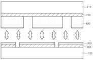
도 5 및 도 6을 참조하여, 상기 지지기판(100)과 상기 캐리어 기판(110)의 본딩공정을 진행한다.5 and 6, the bonding process of the
상기 본딩공정에 의하여 상기 지지기판(100)과 상기 캐리어 기판(110)은 일체가 된다.By the bonding process, the
상기 본딩공정은 상기 지지기판(100) 상에 형성된 전도성 접착층(300)과 상기 캐리어 기판(110)의 광 흡수층(400)을 마주하도록 위치시킨 후 진행할 수 있다.The bonding process may be performed after positioning the conductive
특히, 상기 본딩공정 시 열 또는 압력이 인가되어 상기 지지기판(100)과 상기 캐리어 기판(110)의 본딩력을 향상시킬 수도 있다.In particular, heat or pressure may be applied during the bonding process to improve the bonding force between the
상기 전도성 접착층(300)에 의하여 상기 후면전극층(200) 상에 상기 광 흡수 층(400)이 형성될 수 있다.The light
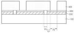
도 7을 참조하여, 상기 캐리어 기판(110) 및 서브 전극층(210)이 제거되고, 상기 광 흡수층(400)이 노출될 수 있다.Referring to FIG. 7, the
상기 캐리어 기판(110) 및 서브 전극층(210)은 리프트 오프(lift-off)를 통해 상기 광 흡수층(400)에서 제거될 수 있다.The
따라서, 상기 지지기판(100) 상에는 후면전극층(200), 전도성 접착층(300), 광 흡수층(400)이 적층된 상태가 된다.Therefore, the
상기 전도성 접착층(300)은 전도성 물질이므로 상기 후면전극층(200) 및 광 흡수층(400)은 전기적으로 연결될 수 있다.Since the conductive
또한, 상기 후면전극층(200)의 제1 관통홀(P1)과 상기 광 흡수층(400)의 제2 관통홀(P2)은 인접하여 형성될 수 있다.In addition, the first through hole P1 of the
예를 들어, 상기 제1 관통홀(P1)과 상기 제2 관통홀(P2)은 제1 갭(G1)은 약 80±20㎛일 수 있다.For example, a first gap G1 of the first through hole P1 and the second through hole P2 may be about 80 ± 20 μm.
상기와 같이 광 흡수층(400)은 별도의 캐리어 기판(110)에 형성한 후, 상기 지지기판(100)과 본딩하여 상기 후면전극층(200) 상에 광 흡수층(400)이 형성될 수 있다.As described above, the
이에 따라, 상기 지지기판(100)에는 광 흡수층 형성을 위한 고온공정이 진행되지 않으므로, 상기 지지기판(100)의 디펙트를 방지할 수 있다.Accordingly, since the high temperature process for forming the light absorbing layer is not performed on the
또한, 상기 지지기판(100)에 고온공정이 인가되지 않으므로, 상기 지지기판(100)은 경량화, 슬림화될 수 있다.In addition, since a high temperature process is not applied to the
또한, 상기 광 흡수층(400)이 캐리어 기판(110)에서 형성되므로 고온공정의 진행이 가능하여, 상기 광 흡수층(400)을 이루는 CIGS 화합물의 결정화를 높일 수 있다.In addition, since the
이에 따라, 상기 광 흡수층(400)의 전기적 특성을 향상시킬 수 있다.Accordingly, the electrical characteristics of the
도 8을 참조하여, 상기 광 흡수층(400)의 표면을 따라 버퍼층(500) 및 고저항 버퍼층(600)이 적층된다.Referring to FIG. 8, a
상기 버퍼층(500) 및 고저항 버퍼층(600)은 상기 광 흡수층(400)의 상면 및 측면에만 선택적으로 형성되어, 상기 제2 관통홀(P2)의 바닥면인 상기 전도성 접착층(300)의 일부를 선택적으로 노출시킬 수 있다.The
예를 들어, 상기 버퍼층(500)을 상기 광 흡수층(400) 및 제2 관통홀(P2)의 표면 프로파일을 따라 형성한 후, 상기 고저항 버퍼층(600)을 상기 버퍼층의 표면 프로파일을 따라 형성한다.For example, after forming the
그리고, 상기 제2 관통홀(P2)의 바닥면인 상기 전도성 접착층(300)이 노출되도록 스크라이빙 공정을 진행할 수 있다. 상기 스크라이빙 공정은 레이저 또는 기계적 패터닝으로 진행될 수 있다.In addition, a scribing process may be performed to expose the conductive
이때, 상기 제2 관통홀(P2)은 상기 전도성 접착층(300)의 표면을 노출시킬 수도 있지만, 상기 후면전극층(200)의 표면을 노출시키도록 형성될 수 있다.In this case, the second through hole P2 may expose the surface of the conductive
상기 버퍼층(500)은 상기 광 흡수층(400) 상에 적어도 하나 이상의 층으로 형성될 수 있다. 상기 버퍼층은 CBD 공정을 통해 황화 카드뮴(CdS)이 적층되어 형성될 수 있다.The
이때, 상기 버퍼층(500)은 n형 반도체 층이고, 상기 광 흡수층(400)은 p형 반도체 층이다. 따라서, 상기 광 흡수층(400) 및 버퍼층(500)은 pn접합을 형성한다.In this case, the
특히, 상기 버퍼층(500)은 상기 광 흡수층(400)의 상면 및 측면을 감싸도록 형성되고, 상기 버퍼층(500)과 광 흡수층(400)의 접촉면적은 확장될 수 있다.In particular, the
이에 따라, pn 접합 영역이 확장되고, 광 전하 발생률을 높일 수 있다.As a result, the pn junction region can be expanded to increase the photocharge generation rate.
또한, 상기 버퍼층(500)이 상기 광 흡수층(400)의 표면에만 선택적으로 형성되어 있으므로, 인접하는 셀간의 누설전류를 방지할 수 있다.In addition, since the
상기 고저항 버퍼층(600)은 산화 아연(ZnO)를 타겟으로 한 스퍼터링 공정을 진행하여, 상기 황화 카드뮴(CdS) 상에 산화 아연층이 더 형성될 수 있다.The high
상기 고저항 버퍼층(600)은 상기 버퍼층(500) 상에 투명전극층으로 형성될 수 있다.The high
예를 들어, 상기 고저항 버퍼층(600)은 ITO, ZnO 및 i-ZnO 중 어느 하나로 형성될 수 있다.For example, the high
상기 버퍼층(500) 및 고저항 버퍼층(600)은 상기 광 흡수층(400)과 이후 형성된 전면전극의 사이에 배치된다.The
즉, 상기 광 흡수층(400)과 전면전극층은 격자상수와 에너지 밴드 갭의 차이가 크기 때문에, 밴드 갭이 두 물질의 중간에 위치하는 상기 버퍼층(500) 및 고저항 버퍼층을 삽입하여 양호한 접합을 형성할 수 있다.That is, since the difference between the lattice constant and the energy band gap between the light absorbing
본 실시예에서는 두 개의 버퍼층(500)을 상기 광 흡수층(400) 상에 형성하였 지만, 이에 한정되지 않고, 상기 버퍼층(500)은 한개의 층으로만 형성될 수 있다.In the present exemplary embodiment, two
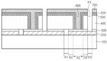
도 9를 참조하여, 상기 제2 관통홀(P2)을 포함하는 상기 고저항 버퍼층(600) 상에 투명한 도전물질을 적층하여 전면전극층(700)이 형성된다.Referring to FIG. 9, a
상기 전면전극층(700)이 형성될 때, 상기 투명한 도전물질이 상기 제2 관통홀(P2)에도 삽입되어 접속배선(800)을 형성할 수 있다. 즉, 상기 접속배선(800)은 상기 전도성 접착층(300)과 접촉할 수 있다.When the
상기 전면전극층(700)은 스퍼터링 공정을 진행하여 알루미늄(Al) 또는 알루미나(Aㄴl2O3)로 도핑된 산화 아연으로 형성된다.The
상기 전면전극층(700)은 상기 광 흡수층(400)과 pn접합을 형성하는 윈도우(window)층으로서, 태양전지 전면의 투명전극의 기능을 하기 때문에 광투과율이 높고 전기 전도성이 좋은 산화 아연(ZnO)으로 형성된다.The
따라서, 상기 산화 아연에 알루미늄 또는 알루미나를 도핑함으로써 낮은 저항값을 갖는 전극을 형성할 수 있다.Therefore, it is possible to form an electrode having a low resistance value by doping aluminum or alumina to the zinc oxide.
상기 전면전극층(700)인 산화 아연 박막은 RF 스퍼터링방법으로 ZnO 타겟을 사용하여 증착하는 방법과 Zn 타겟을 이용한 반응성 스퍼터링, 그리고 유기금속화학증착법 등으로 형성될 수 있다.The zinc oxide thin film as the
또한, 전기광학적 특성이 뛰어난 ITO(Indium Thin Oxide) 박막을 산화 아연 박막 상에 층착한 2중 구조를 형성할 수도 있다.In addition, a double structure in which an indium thin oxide (ITO) thin film having excellent electro-optic properties is laminated on a zinc oxide thin film may be formed.
상기 접속배선(800)에 의해 각각의 셀은 서로 연결될 수 있다. 즉, 상기 접속배선(800)은 상호 인접하는 셀의 후면전극층(200)과 전면전극층(700)을 물리적, 전기적으로 연결할 수 있다.Each cell may be connected to each other by the
도시되지는 않았지만, 상기 접속배선(800)은 상기 제2 관통홀(P2)을 통해 상기 후면전극층(200)과 직접 접촉할 수도 있다. 이에 따라, 상기 접속배선(800)과 상기 후면전극층(200)의 콘택특성을 향상시킬 수 있다.Although not shown, the
상기 접속배선(800)의 주위에 상기 버퍼층(500) 및 고저항 버퍼층(600)이 형성되어 있으므로, 상기 접속배선(800)과 후면전극층(200)의 전기적 접합특성이 향상되어 전류의 이동이 양호할 수 있다.Since the
즉, 상기 광 흡수층(400)과 상기 접속배선(800) 사이에 버퍼층(500) 및 고저항 버퍼층(600)이 배치되어 있으므로, 상기 접속배선(800)의 리키지 커런트 발생을 완전히 차단시키고 직렬저항 성분을 감소시킴으로써 태양전지의 전기적 특성을 향상시킬 수 있다.That is, since the
도 10을 참조하여, 상기 전면전극층(700), 고저항 버퍼층(600), 버퍼층(500) 및 광 흡수층(400)을 관통하는 제3 관통홀(P3)이 형성된다.Referring to FIG. 10, a third through hole P3 penetrating the
상기 제3 관통홀(P3)은 상기 후면전극층(200)을 선택적으로 노출시킬 수 있다. 상기 제3 관통홀(P3)은 상기 제2 관통홀(P2)과 인접하도록 형성될 수 있다.The third through hole P3 may selectively expose the
예를 들어, 상기 제2 관통홀(P2)과 제3 관통홀(P3)의 제2 갭(G2)은 80±20일 수 있다.For example, the second gap G2 of the second through hole P2 and the third through hole P3 may be 80 ± 20.
상기 제3 관통홀(P3)은 레이저(laser)를 조사(irradiate)하거나, 팁(Tip)과 같은 물리적인(mechanical) 방법으로 형성할 수 있다.The third through hole P3 may be formed by irradiating a laser or by a mechanical method such as a tip.
따라서, 상기 제3 관통홀(P3)에 의하여 상기 광 흡수층(400), 버퍼층(500), 고저항 버퍼층(600) 및 전면전극층(700)은 단위 셀별로 분리될 수 있다.Accordingly, the
실시예에 따른 태양전지 및 이의 제조방법에 의하여 태양전지의 전기적인 특성 및 신뢰성을 향상시킬 수 있다.By the solar cell and the method of manufacturing the same according to the embodiment it is possible to improve the electrical characteristics and reliability of the solar cell.
이상에서 실시예를 중심으로 설명하였으나 이는 단지 예시일 뿐 본 발명을 한정하는 것이 아니며, 본 발명이 속하는 분야의 통상의 지식을 가진 자라면 본 실시예의 본질적인 특성을 벗어나지 않는 범위에서 이상에 예시되지 않은 여러 가지의 변형과 응용이 가능함을 알 수 있을 것이다. 예를 들어, 실시예에 구체적으로 나타난 각 구성 요소는 변형하여 실시할 수 있는 것이다. 그리고 이러한 변형과 응용에 관계된 차이점들은 첨부된 청구 범위에서 규정하는 본 발명의 범위에 포함되는 것으로 해석되어야 할 것이다.While the present invention has been particularly shown and described with reference to exemplary embodiments thereof, it is to be understood that the invention is not limited to the disclosed exemplary embodiments, but, on the contrary, It will be understood that various modifications and applications are possible. For example, each component specifically shown in the embodiments can be modified and implemented. It is to be understood that all changes and modifications that come within the meaning and range of equivalency of the claims are therefore intended to be embraced therein.
도 1 내지 도 10는 실시예에 따른 태양전지의 제조방법을 나타내는 단면도이다.1 to 10 are cross-sectional views showing a method of manufacturing a solar cell according to the embodiment.
Claims (11)
Translated fromKoreanPriority Applications (6)
| Application Number | Priority Date | Filing Date | Title |
|---|---|---|---|
| KR1020090104468AKR101173344B1 (en) | 2009-10-30 | 2009-10-30 | Solar cell and mehtod of fabricating the same |
| US13/380,313US9171979B2 (en) | 2009-10-30 | 2010-11-01 | Battery and solar method for manufacturing the same |
| JP2012536700AJP5624152B2 (en) | 2009-10-30 | 2010-11-01 | Solar cell and manufacturing method thereof |
| CN2010800495926ACN102598301A (en) | 2009-10-30 | 2010-11-01 | Solar cell and manufacturing method thereof |
| EP10827161.0AEP2485274B1 (en) | 2009-10-30 | 2010-11-01 | Solar cell and manufacturing method thereof |
| PCT/KR2010/007615WO2011053077A2 (en) | 2009-10-30 | 2010-11-01 | Solar cell and manufacturing method thereof |
Applications Claiming Priority (1)
| Application Number | Priority Date | Filing Date | Title |
|---|---|---|---|
| KR1020090104468AKR101173344B1 (en) | 2009-10-30 | 2009-10-30 | Solar cell and mehtod of fabricating the same |
Publications (2)
| Publication Number | Publication Date |
|---|---|
| KR20110047726A KR20110047726A (en) | 2011-05-09 |
| KR101173344B1true KR101173344B1 (en) | 2012-08-10 |
Family
ID=43922899
Family Applications (1)
| Application Number | Title | Priority Date | Filing Date |
|---|---|---|---|
| KR1020090104468AExpired - Fee RelatedKR101173344B1 (en) | 2009-10-30 | 2009-10-30 | Solar cell and mehtod of fabricating the same |
Country Status (6)
| Country | Link |
|---|---|
| US (1) | US9171979B2 (en) |
| EP (1) | EP2485274B1 (en) |
| JP (1) | JP5624152B2 (en) |
| KR (1) | KR101173344B1 (en) |
| CN (1) | CN102598301A (en) |
| WO (1) | WO2011053077A2 (en) |
Families Citing this family (20)
| Publication number | Priority date | Publication date | Assignee | Title |
|---|---|---|---|---|
| KR101338615B1 (en)* | 2011-10-04 | 2014-01-10 | 엘지이노텍 주식회사 | Solar apparatus and method of fabricating the same |
| KR101241467B1 (en) | 2011-10-13 | 2013-03-11 | 엘지이노텍 주식회사 | Solar cell and preparing method of the same |
| KR101896951B1 (en)* | 2011-10-13 | 2018-09-12 | 엘지이노텍 주식회사 | Solar cell and method for fabricating unsing the same |
| KR101305665B1 (en)* | 2011-10-17 | 2013-09-09 | 엘지이노텍 주식회사 | Solar cell module apparatus and method for fabricating of the same |
| US20130118569A1 (en)* | 2011-11-14 | 2013-05-16 | Taiwan Semiconductor Manufacturing Co., Ltd. | Method for forming thin film solar cell with buffer-free fabrication process |
| KR20130109330A (en) | 2012-03-27 | 2013-10-08 | 엘지이노텍 주식회사 | Solar cell and method of fabricating the same |
| US8809109B2 (en)* | 2012-05-21 | 2014-08-19 | Stion Corporation | Method and structure for eliminating edge peeling in thin-film photovoltaic absorber materials |
| KR20130136739A (en) | 2012-06-05 | 2013-12-13 | 엘지이노텍 주식회사 | Solar cell and method of fabricating the same |
| KR101393859B1 (en)* | 2012-06-28 | 2014-05-13 | 엘지이노텍 주식회사 | Solar cell and method of fabricating the same |
| US8987590B2 (en) | 2012-08-01 | 2015-03-24 | International Business Machines Corporation | Thin film solar cells |
| KR102098100B1 (en)* | 2013-09-17 | 2020-04-08 | 엘지이노텍 주식회사 | Solar cell and method of fabricating the same |
| KR20150031889A (en)* | 2013-09-17 | 2015-03-25 | 엘지이노텍 주식회사 | Solar cell |
| KR20150039536A (en)* | 2013-10-02 | 2015-04-10 | 엘지이노텍 주식회사 | Solar cell |
| KR20150093291A (en)* | 2014-02-06 | 2015-08-18 | 주성엔지니어링(주) | Photovoltaic with improved visibility and method for manufacturing thereof |
| US10453978B2 (en)* | 2015-03-12 | 2019-10-22 | International Business Machines Corporation | Single crystalline CZTSSe photovoltaic device |
| CN104993013B (en)* | 2015-05-25 | 2017-12-19 | 北京四方继保自动化股份有限公司 | A kind of full laser grooving and scribing method of large area CIGS Thinfilm solar cell assembly |
| US9935214B2 (en) | 2015-10-12 | 2018-04-03 | International Business Machines Corporation | Liftoff process for exfoliation of thin film photovoltaic devices and back contact formation |
| JP7058460B2 (en)* | 2016-06-30 | 2022-04-22 | ソーラーフロンティア株式会社 | Photoelectric conversion module |
| JP2018056397A (en)* | 2016-09-29 | 2018-04-05 | 日亜化学工業株式会社 | Method for manufacturing metal base substrate, method for manufacturing semiconductor device, metal base substrate, and semiconductor device |
| CN110574170B (en)* | 2018-06-20 | 2023-04-11 | 天津三安光电有限公司 | Flexible thin film solar cell and manufacturing method thereof |
Citations (3)
| Publication number | Priority date | Publication date | Assignee | Title |
|---|---|---|---|---|
| JP2007123532A (en) | 2005-10-27 | 2007-05-17 | Honda Motor Co Ltd | Solar cell |
| JP2007317885A (en) | 2006-05-25 | 2007-12-06 | Honda Motor Co Ltd | Solar cell and method for manufacturing the same |
| JP2007317858A (en) | 2006-05-25 | 2007-12-06 | Honda Motor Co Ltd | Chalcopyrite solar cell and method for manufacturing the same |
Family Cites Families (11)
| Publication number | Priority date | Publication date | Assignee | Title |
|---|---|---|---|---|
| US4892592A (en) | 1987-03-26 | 1990-01-09 | Solarex Corporation | Thin film semiconductor solar cell array and method of making |
| DE4333407C1 (en) | 1993-09-30 | 1994-11-17 | Siemens Ag | Solar cell comprising a chalcopyrite absorber layer |
| US20090111206A1 (en)* | 1999-03-30 | 2009-04-30 | Daniel Luch | Collector grid, electrode structures and interrconnect structures for photovoltaic arrays and methods of manufacture |
| JP2002094089A (en) | 2000-09-11 | 2002-03-29 | Honda Motor Co Ltd | Method for manufacturing compound thin film solar cell |
| US6563893B2 (en) | 2001-05-17 | 2003-05-13 | Ut-Battelle, Llc | Carrier-frequency synchronization system for improved amplitude modulation and television broadcast reception |
| JP2002343564A (en) | 2001-05-18 | 2002-11-29 | Sharp Corp | Transfer film and method of manufacturing organic electroluminescence device using the same |
| JP2005032917A (en)* | 2003-07-10 | 2005-02-03 | Dainippon Printing Co Ltd | Organic thin film solar cell manufacturing method and transfer sheet |
| JP4681352B2 (en)* | 2005-05-24 | 2011-05-11 | 本田技研工業株式会社 | Chalcopyrite solar cell |
| US8900970B2 (en)* | 2006-04-28 | 2014-12-02 | Semiconductor Energy Laboratory Co., Ltd. | Method for manufacturing a semiconductor device using a flexible substrate |
| EP1933343A1 (en) | 2006-12-13 | 2008-06-18 | Sony Deutschland Gmbh | A method of preparing a porous semiconductor film on a substrate |
| KR101494153B1 (en) | 2007-12-21 | 2015-02-23 | 주성엔지니어링(주) | Thin film solar cell and its manufacturing method |
- 2009
- 2009-10-30KRKR1020090104468Apatent/KR101173344B1/ennot_activeExpired - Fee Related
- 2010
- 2010-11-01WOPCT/KR2010/007615patent/WO2011053077A2/enactiveApplication Filing
- 2010-11-01USUS13/380,313patent/US9171979B2/ennot_activeExpired - Fee Related
- 2010-11-01CNCN2010800495926Apatent/CN102598301A/enactivePending
- 2010-11-01JPJP2012536700Apatent/JP5624152B2/ennot_activeExpired - Fee Related
- 2010-11-01EPEP10827161.0Apatent/EP2485274B1/ennot_activeNot-in-force
Patent Citations (3)
| Publication number | Priority date | Publication date | Assignee | Title |
|---|---|---|---|---|
| JP2007123532A (en) | 2005-10-27 | 2007-05-17 | Honda Motor Co Ltd | Solar cell |
| JP2007317885A (en) | 2006-05-25 | 2007-12-06 | Honda Motor Co Ltd | Solar cell and method for manufacturing the same |
| JP2007317858A (en) | 2006-05-25 | 2007-12-06 | Honda Motor Co Ltd | Chalcopyrite solar cell and method for manufacturing the same |
Also Published As
| Publication number | Publication date |
|---|---|
| WO2011053077A3 (en) | 2011-10-13 |
| US20120199191A1 (en) | 2012-08-09 |
| US9171979B2 (en) | 2015-10-27 |
| EP2485274A4 (en) | 2013-09-18 |
| WO2011053077A2 (en) | 2011-05-05 |
| EP2485274B1 (en) | 2014-09-17 |
| JP5624152B2 (en) | 2014-11-12 |
| CN102598301A (en) | 2012-07-18 |
| EP2485274A2 (en) | 2012-08-08 |
| JP2013509706A (en) | 2013-03-14 |
| KR20110047726A (en) | 2011-05-09 |
Similar Documents
| Publication | Publication Date | Title |
|---|---|---|
| KR101173344B1 (en) | Solar cell and mehtod of fabricating the same | |
| KR101081294B1 (en) | Solar cell and method of fabricating the same | |
| CN102549772B (en) | Solar cell device and manufacture method thereof | |
| KR101172132B1 (en) | Solar cell and method of fabricating the same | |
| KR101154763B1 (en) | Solar cell and method of fabricating the same | |
| KR101072089B1 (en) | Solar cell and method of fabircating the same | |
| KR101091258B1 (en) | Solar cell and manufacturing method thereof | |
| KR101091475B1 (en) | Solar cell and manufacturing method thereof | |
| KR101034150B1 (en) | Solar cell and manufacturing method thereof | |
| KR101081143B1 (en) | Solar cell and method of fabricating the same | |
| KR101592582B1 (en) | Solar cell and manufacturing method thereof | |
| JP5602234B2 (en) | Photovoltaic power generation apparatus and manufacturing method thereof | |
| JP5624153B2 (en) | Solar cell and manufacturing method thereof | |
| KR20110047724A (en) | Solar cell and manufacturing method thereof | |
| KR101034146B1 (en) | Solar cell and manufacturing method thereof | |
| KR101072170B1 (en) | Solar cell and method of fabricating the same | |
| KR101063721B1 (en) | Solar cell and manufacturing method thereof | |
| KR101081175B1 (en) | Solar cell and method of fabricating the same | |
| KR101072067B1 (en) | Tip, solar cell and method of fabricating the solar cell using the tip | |
| KR101091499B1 (en) | Tip, the solar cell and method of fabricating the solar cell using the tip | |
| KR101543034B1 (en) | Tip and manufacturing method of solar cell using the same | |
| KR20110036353A (en) | Solar cell and manufacturing method thereof |
Legal Events
| Date | Code | Title | Description |
|---|---|---|---|
| A201 | Request for examination | ||
| PA0109 | Patent application | St.27 status event code:A-0-1-A10-A12-nap-PA0109 | |
| PA0201 | Request for examination | St.27 status event code:A-1-2-D10-D11-exm-PA0201 | |
| R18-X000 | Changes to party contact information recorded | St.27 status event code:A-3-3-R10-R18-oth-X000 | |
| D13-X000 | Search requested | St.27 status event code:A-1-2-D10-D13-srh-X000 | |
| D14-X000 | Search report completed | St.27 status event code:A-1-2-D10-D14-srh-X000 | |
| E902 | Notification of reason for refusal | ||
| PE0902 | Notice of grounds for rejection | St.27 status event code:A-1-2-D10-D21-exm-PE0902 | |
| PG1501 | Laying open of application | St.27 status event code:A-1-1-Q10-Q12-nap-PG1501 | |
| P11-X000 | Amendment of application requested | St.27 status event code:A-2-2-P10-P11-nap-X000 | |
| P13-X000 | Application amended | St.27 status event code:A-2-2-P10-P13-nap-X000 | |
| E902 | Notification of reason for refusal | ||
| PE0902 | Notice of grounds for rejection | St.27 status event code:A-1-2-D10-D21-exm-PE0902 | |
| E13-X000 | Pre-grant limitation requested | St.27 status event code:A-2-3-E10-E13-lim-X000 | |
| P11-X000 | Amendment of application requested | St.27 status event code:A-2-2-P10-P11-nap-X000 | |
| P13-X000 | Application amended | St.27 status event code:A-2-2-P10-P13-nap-X000 | |
| E701 | Decision to grant or registration of patent right | ||
| PE0701 | Decision of registration | St.27 status event code:A-1-2-D10-D22-exm-PE0701 | |
| GRNT | Written decision to grant | ||
| PR0701 | Registration of establishment | St.27 status event code:A-2-4-F10-F11-exm-PR0701 | |
| PR1002 | Payment of registration fee | St.27 status event code:A-2-2-U10-U11-oth-PR1002 Fee payment year number:1 | |
| PG1601 | Publication of registration | St.27 status event code:A-4-4-Q10-Q13-nap-PG1601 | |
| P22-X000 | Classification modified | St.27 status event code:A-4-4-P10-P22-nap-X000 | |
| PN2301 | Change of applicant | St.27 status event code:A-5-5-R10-R13-asn-PN2301 St.27 status event code:A-5-5-R10-R11-asn-PN2301 | |
| FPAY | Annual fee payment | Payment date:20150706 Year of fee payment:4 | |
| PR1001 | Payment of annual fee | St.27 status event code:A-4-4-U10-U11-oth-PR1001 Fee payment year number:4 | |
| FPAY | Annual fee payment | Payment date:20160707 Year of fee payment:5 | |
| PR1001 | Payment of annual fee | St.27 status event code:A-4-4-U10-U11-oth-PR1001 Fee payment year number:5 | |
| R18-X000 | Changes to party contact information recorded | St.27 status event code:A-5-5-R10-R18-oth-X000 | |
| FPAY | Annual fee payment | Payment date:20170704 Year of fee payment:6 | |
| PR1001 | Payment of annual fee | St.27 status event code:A-4-4-U10-U11-oth-PR1001 Fee payment year number:6 | |
| R18-X000 | Changes to party contact information recorded | St.27 status event code:A-5-5-R10-R18-oth-X000 | |
| LAPS | Lapse due to unpaid annual fee | ||
| PC1903 | Unpaid annual fee | St.27 status event code:A-4-4-U10-U13-oth-PC1903 Not in force date:20180807 Payment event data comment text:Termination Category : DEFAULT_OF_REGISTRATION_FEE | |
| PC1903 | Unpaid annual fee | St.27 status event code:N-4-6-H10-H13-oth-PC1903 Ip right cessation event data comment text:Termination Category : DEFAULT_OF_REGISTRATION_FEE Not in force date:20180807 | |
| R18-X000 | Changes to party contact information recorded | St.27 status event code:A-5-5-R10-R18-oth-X000 | |
| PN2301 | Change of applicant | St.27 status event code:A-5-5-R10-R13-asn-PN2301 St.27 status event code:A-5-5-R10-R11-asn-PN2301 | |
| P22-X000 | Classification modified | St.27 status event code:A-4-4-P10-P22-nap-X000 |