KR101162192B1 - Reduction of etching charge damage in manufacture of microelectromechanical devices - Google Patents
Reduction of etching charge damage in manufacture of microelectromechanical devicesDownload PDFInfo
- Publication number
- KR101162192B1 KR101162192B1KR1020067023026AKR20067023026AKR101162192B1KR 101162192 B1KR101162192 B1KR 101162192B1KR 1020067023026 AKR1020067023026 AKR 1020067023026AKR 20067023026 AKR20067023026 AKR 20067023026AKR 101162192 B1KR101162192 B1KR 101162192B1
- Authority
- KR
- South Korea
- Prior art keywords
- conductive layer
- conductive
- layer
- layers
- wire
- Prior art date
- Legal status (The legal status is an assumption and is not a legal conclusion. Google has not performed a legal analysis and makes no representation as to the accuracy of the status listed.)
- Expired - Fee Related
Links
Images


Classifications
- B—PERFORMING OPERATIONS; TRANSPORTING
- B81—MICROSTRUCTURAL TECHNOLOGY
- B81C—PROCESSES OR APPARATUS SPECIALLY ADAPTED FOR THE MANUFACTURE OR TREATMENT OF MICROSTRUCTURAL DEVICES OR SYSTEMS
- B81C1/00—Manufacture or treatment of devices or systems in or on a substrate
- B81C1/00436—Shaping materials, i.e. techniques for structuring the substrate or the layers on the substrate
- B81C1/00555—Achieving a desired geometry, i.e. controlling etch rates, anisotropy or selectivity
- B81C1/00563—Avoid or control over-etching
- B81C1/00579—Avoid charge built-up
- B—PERFORMING OPERATIONS; TRANSPORTING
- B81—MICROSTRUCTURAL TECHNOLOGY
- B81C—PROCESSES OR APPARATUS SPECIALLY ADAPTED FOR THE MANUFACTURE OR TREATMENT OF MICROSTRUCTURAL DEVICES OR SYSTEMS
- B81C1/00—Manufacture or treatment of devices or systems in or on a substrate
- B—PERFORMING OPERATIONS; TRANSPORTING
- B81—MICROSTRUCTURAL TECHNOLOGY
- B81B—MICROSTRUCTURAL DEVICES OR SYSTEMS, e.g. MICROMECHANICAL DEVICES
- B81B3/00—Devices comprising flexible or deformable elements, e.g. comprising elastic tongues or membranes
- B81B3/0002—Arrangements for avoiding sticking of the flexible or moving parts
- B81B3/0008—Structures for avoiding electrostatic attraction, e.g. avoiding charge accumulation
- Y—GENERAL TAGGING OF NEW TECHNOLOGICAL DEVELOPMENTS; GENERAL TAGGING OF CROSS-SECTIONAL TECHNOLOGIES SPANNING OVER SEVERAL SECTIONS OF THE IPC; TECHNICAL SUBJECTS COVERED BY FORMER USPC CROSS-REFERENCE ART COLLECTIONS [XRACs] AND DIGESTS
- Y10—TECHNICAL SUBJECTS COVERED BY FORMER USPC
- Y10T—TECHNICAL SUBJECTS COVERED BY FORMER US CLASSIFICATION
- Y10T428/00—Stock material or miscellaneous articles
- Y10T428/12—All metal or with adjacent metals
- Y10T428/12493—Composite; i.e., plural, adjacent, spatially distinct metal components [e.g., layers, joint, etc.]
- Y10T428/12535—Composite; i.e., plural, adjacent, spatially distinct metal components [e.g., layers, joint, etc.] with additional, spatially distinct nonmetal component
- Y10T428/12542—More than one such component
Landscapes
- Engineering & Computer Science (AREA)
- Microelectronics & Electronic Packaging (AREA)
- Manufacturing & Machinery (AREA)
- Computer Hardware Design (AREA)
- Physics & Mathematics (AREA)
- Geometry (AREA)
- Micromachines (AREA)
- Mechanical Light Control Or Optical Switches (AREA)
- Electrostatic, Electromagnetic, Magneto- Strictive, And Variable-Resistance Transducers (AREA)
Abstract
Translated fromKoreanDescription
Translated fromKorean본 발명은 미소 기전 기기(microelectromechanical devices)를 제조하는 방법 및 장치에 관한 것이다.FIELD OF THE INVENTION The present invention relates to methods and apparatus for manufacturing microelectromechanical devices.
미소 기전 시스템(microelectromechanical systems, MEMS) 기기는 박막 공정들로부터 제조될 수 있다. 이들 공정은 층들에 침적되는 일련의 박막을 포함할 수 있으며, 층들을 패터닝 및 에칭하여 기기를 형성한다. 기기가 움직할 수 있도록 하기 위해, 하나의 층은 분리층(isolation layer)일 수 있다. 분리층은 구조적 부재(structural member)로서 작용하는 기기의 층들을 형성할 때 사용되는 것이지만, 기기가 완성될 때 제거될 수 있다.Microelectromechanical systems (MEMS) devices can be manufactured from thin film processes. These processes can include a series of thin films deposited on the layers, patterning and etching the layers to form the device. In order to allow the device to move, one layer may be an isolation layer. The separating layer is used to form layers of the device that act as structural members, but can be removed when the device is completed.
분리층의 제거는 에칭제로서 희생층 재료에만 작용하는 재료를 사용하는 에칭 공정을 포함할 수 있다. 몇몇 경우에, 분리층은 건식 가스 에칭으로 제거될 수 있는 산화물(oxide)일 수 있다. 다른 형태의 분리층은 또한 다른 제거 방법을 사용할 수도 있다. 분리층의 제거로 일반적으로 갭(gap)이 생기며, 이 갭을 통해 기기의 부재가 작동(actuation) 시에 움직일 것이다.Removal of the separation layer may include an etching process using a material that acts only on the sacrificial layer material as an etchant. In some cases, the separation layer may be an oxide that can be removed by dry gas etching. Other types of separation layers may also use other removal methods. The removal of the separation layer generally creates a gap through which the member of the device will move during actuation.
MEMS 기기는 종종 갭에 의해 분리되어 있는 제1 전도층과 제2 전도층 사이의 전압차를 발생시키는 전기 신호의 사용에 의해 작동한다. 분리층을 건식 가스 에칭하는 중에, 층들에 정전하(electrostatic charge)가 축적될 수 있다. 심한 경우, 상기 두 개의 층이 서로 고착되어 기기가 동작하지 않게 될 수 있다. 덜 심한 경우, 가동 소자(movable elecmet)가 손상되거나 변형되고, 이어서 올바르게 동작하지 않을 수 있다.MEMS devices often operate by the use of electrical signals that generate a voltage difference between the first conductive layer and the second conductive layer separated by a gap. During dry gas etching the separation layer, electrostatic charge may accumulate in the layers. In severe cases, the two layers may stick to each other and the device may become inoperable. In less severe cases, the movable elecmet may be damaged or deformed and then not function properly.
본 발명의 일 양태에 따르면, 미소 기전 기기(microelectromechanical device)를 제조하는 방법이 제공된다. 미소 기전 긱기의 제조 방법은 기판 상에 적어도 제1 전도층 및 제2 전도층을 형성하는 단계; 상기 제1 전도층과 상기 제2 전도층 사이에 분리층을 형성하는 단계; 상기 제1 전도층과 상기 제2 전도층을 전기적으로 함께 결합하는 단계; 및 상기 분리층을 제거하여 상기 제1 전도층과 상기 제2 전도층 사이에 갭(gap)을 형성하는 단계를 포함한다.According to one aspect of the present invention, a method of manufacturing a microelectromechanical device is provided. The method of making microelectromechanical devices includes forming at least a first conductive layer and a second conductive layer on a substrate; Forming a separation layer between the first conductive layer and the second conductive layer; Electrically coupling the first conductive layer and the second conductive layer together; And removing the separation layer to form a gap between the first conductive layer and the second conductive layer.
또한, 본 발명의 다른 양태에 따르면, 미소 기전 기기를 제조하는 장치로서, 에칭 공정 이전에, 적어도 두 개의 전도층을 전기적으로 함께 연결하도록 구성된 전도성 와이어를 포함하며, 상기 적어도 두 개의 전도층은 상기 미소 기전 기기의 적어도 일부를 형성하는, 미소 기전 기기의 제조 장치가 제공된다.According to another aspect of the invention, there is also provided an apparatus for manufacturing a microvoltaic device, comprising a conductive wire configured to electrically connect at least two conductive layers together before an etching process, the at least two conductive layers being There is provided an apparatus for producing a micromechanical device, which forms at least a portion of the micromechanical device.
첨부도면을 참조하여 개시 내용을 읽으면 본 발명을 가장 잘 이해할 수 있다.The present invention may be best understood by reading the disclosure with reference to the accompanying drawings.
도 1은 분리층을 사용하여 형성된 미소 기전 기기의 일 실시예를 나타낸 도면이다. 1 shows an embodiment of a microvoltaic device formed using a separation layer.
도 2는 에치 공정 중의 정전하 축적에 의해 동작 불가능하게 되는 미소 기전 기기의 일 실시예를 나타낸 도면이다.FIG. 2 is a diagram showing an embodiment of a microvoltaic device which becomes inoperable due to static charge accumulation during an etch process.
도 3은 에칭 공정 동안의 정전하 축적의 효과를 완화시키는 장치의 일 실시예를 나타낸 도면이다.3 shows one embodiment of an apparatus that mitigates the effects of static charge accumulation during an etching process.
도 4는 에칭 공정 중의 정전하 축적의 효과를 완화시키는 장치의 다른 실시예를 나타낸 도면이다.4 shows another embodiment of an apparatus for mitigating the effects of static charge accumulation during an etching process.
도 5는 일 실시예의 미소 기전 기기를 제조하는 방법의 흐름도이다.5 is a flowchart of a method of manufacturing the micromechanical device of one embodiment.
도 6a 및 도 6b는 에칭 공정 중의 정전하 축적의 효과를 완화시키는 다른 장치의 실시예를 나타낸 도면이다.6A and 6B illustrate an embodiment of another apparatus that mitigates the effects of static charge accumulation during an etching process.
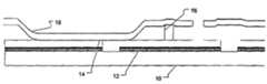
도 1은 분리층을 포함하는 박막 공정으로 형성되는 미소 기전 기기의 일례를 나타낸 것이다. 이 특정 예는 간섭 변조기(interferometric modulator)에 대한 것이지만, 본 발명의 실시예들은 분리층을 가지는 박막 공정으로 형성되는 각종 MEMS 기기에 적용 가능하다. 간섭 변조기는 투명 기판(10) 상에 형성된다. 도면부호 12 및 14와 같은 일반적으로 금속 및 산화물의 층을 포함하는 광 스택(optical stack)이 투명 기판(10) 위에 형성된다. 희생층(sacrificial layer)이 처리중에 전도층들을 서로 전기적으로 분리시키는 작용을 할 때, 희생층을 분리층이라고도 할 수 있다. 멤브레인(membrane)을 형성하기 이전에, 분리층에 비아(via)를 패터 닝하여, 멤브레인의 금속이 비아에 채워져 도면부호 16과 같은 포스트(post)가 형성되도록 해준다.1 illustrates an example of a micromechanical device formed by a thin film process including a separation layer. Although this particular example is for an interferometric modulator, embodiments of the present invention are applicable to a variety of MEMS devices formed by thin film processes with separation layers. The interferometric modulator is formed on the
금속의 멤브레인(18)과 같은 변조기 구조물이 완성될 때, 분리층을 제거한다. 이것은 멤브레인(18)의 부분(portion)이 광 스택의 전극층(12) 쪽으로 편향될 수 있도록 해준다. 간섭 변조기의 경우, 멤브레인(18)과 전극층(12) 사이의 전압 차의 조작에 의해, 멤브레인(18)을 금속의 전극층(12) 쪽으로 끌어당긴다. 전극층(12)과 멤브레인(18)은 여기에서 설명한 것처럼 금속이거나 다른 전도성 재료일 수 있다. 도 1에 도시한 멤브레인의 부분에 의해 형성된 셀(cell)은, 멤브레인(18)에 인가하는 전압과는 다른 전압을 전도층(14)에 인가함으로써 활성화된다. 이것은 멤브레인이 정전기적으로 전극, 또는 제1 전도성의 층(12) 쪽으로 끌어 당겨지게 한다. 전도층은 금속이나 임의의 다른 전도성 재료일 수 있다.When the modulator structure, such as
분리층을 제거하는 동안에, 충분한 정전하가 두 전도층의 표면에 축적되어 멤브레인이 활성화되지 않은 전도층(14) 쪽으로 끌어 당겨질 수 있다. 이 상태를 도 2에 나타냈다. 이것은 정상 상태로는 간섭 변조기의 활성 상태이지만, 다른 점은 전위가 변화할 때 멤브레인이 산화물의 층(12)으로부터 해방되지 않는 것이다. 멤브레인은 영구적으로 활성 상태를 나타낸다. 이것은 전도성의 층(12)와 전도성의 멤브레인(18) 사이의 정전력(electrostatic force)에 의해 심화되는, 종종 정지 마찰(stiction)이라고 하는 고착(sticking)과 마찰(friction)의 결합에 의해 유발될 수 있다. During removal of the separation layer, sufficient static charge may accumulate on the surfaces of the two conductive layers, attracting the membrane towards the inactive
다른 많은 방식으로 분리층을 제거할 수 있다. 일반적으로, 크세논 디플루오르(XeF2) 에칭과 같은 건식 가스 에칭을 사용하여 분리층을 제거한다. 이것은 에칭 공정의 예이고, 임의의 에칭 공정을 사용할 수도 있다. 건조한 환경이 정전하의 축적에 기여하는 것일 수 있다. MEMS 기기를 제조하는데 사용되는 재료나 공정의 기초를 변경하는 것이 아니라, 대신에 정전하 축적을 제거하도록 공정을 적응시키는 것이 나을 것이다.There are many other ways to remove the separation layer. Generally, dry gas etching, such as xenon difluorine (XeF2) etching, is used to remove the separation layer. This is an example of an etching process, and arbitrary etching processes may be used. The dry environment may be contributing to the accumulation of static charges. It would be better to adapt the process to remove static charge buildup instead of changing the basis of the material or process used to manufacture the MEMS device.
습식 에칭 공정 동안에 전도층을 접지시키는 것도 몇 가지 이점이 있다. 접지함으로써, 바람직한 경우에는 인에블(enable)되거나 바람직하지 못한 경우에는 완화되는, 기기 전기화학(device electrochemistry)에 영향이 있을 수 있다. 일 실시예에서, 층들은 함께 접지되어 있고, 분리층은 제거되고, 대신에 접지는 남아서, 기기는 정전하 방전의 우려 없이 안전하게 수송될 수 있다. 이것은 에칭이 습식 에칭 또는 건식 에칭인 경우에 유용할 것이다.Grounding the conductive layer during the wet etching process has several advantages. By grounding, there may be an effect on device electrochemistry, which is enabled in the preferred case or relaxed in the undesirable case. In one embodiment, the layers are grounded together, the isolation layer is removed, and instead the ground remains, so that the device can be safely transported without fear of electrostatic discharge. This would be useful if the etching is a wet etch or a dry etch.
접지 공정(grounding process)은 기기의 구조물에 대해 외부에 있는 장치나 기구에 의한 외부 접지일 수 있다. 다르게는, 접지는 제조하는 동안에 인에이블되는 기기의 내부 구조물의 일부일 수 있다. 처음에, 외부 접지에 대해 설명한다.The grounding process may be external grounding by a device or apparatus external to the structure of the appliance. Alternatively, the ground may be part of the internal structure of the device that is enabled during manufacturing. First, the external ground will be described.
에칭 공정 동안에 정전하의 축적을 완화시키는 장치를 도 3에 도시하였다. 도 4에는 다른 실시예를 도시하였다. 도 3에서, 전도성 와이어(22)는 제1 전도층(14) 및 제2 전도층(18)에 부착되어 이들을 동일한 전위로 유지한다. 동일한 전위는 제1 전도층(14) 및 제2 전도층(18)을 접지면에 부착하거나, 단지 이들을 함께 부착하는 것을 포함할 수 있다. 제1 전도층(14) 및 제2 전도층(18)을 동일한 전위로 유지함으로써, 정전하 축적은 이 두 층간의 차이를 유발시키지 않을 것이므로, 에칭 공정 동안에 멤브레인이 작동하는 문제를 방지될 것이다. 추가로 더욱 상세하게 설명되는 것처럼, 상기 두 층은 에칭 공정에 앞서 임의의 지점에서 전기적으로 결합될 수 있기는 하지만, 이것은 일반적으로 에칭 공정 바로 직전에 수행될 것이다. 전기적 결합을, 기기가 제조되는 기판의 비활성 영역(inactive area)으로 제한하는 것이 바람직할 수 있다.An apparatus that mitigates the accumulation of static charge during the etching process is shown in FIG. 3. 4 shows another embodiment. In FIG. 3,
도 4의 다른 실시예는 세 개의 전도층과 두 개의 분리층으로 제조되는 기기를 나타낸 것이다. 이 실시예의 간섭 변조기에서, 도 1 및 도 3의 제2 전도층(18)에 상당하는 것은 실제로 두 개의 전도층(18a, 18b)이다. 이들은 대개 두 개의 개별 층으로 배치되지만, 물리적으로 또는 전기적으로 서로 연결되어 있다. 이것은 일반적으로 다른 전도층과 연결되는 하나의 연결부(connection)만을 필요로 하는, 플렉스층(flex layer)과 미러층(mirror layer)의 결합일 것이다. 이 특정 구성은, 층(18a)과 전극층(12) 사이에 형성된 것 외에 분리층이 층(18a)과 층(18b) 사이에 형성될 수 있기 때문에, 제1 분리층의 등가물로서 두 개의 분리층을 필요로 할 수 있다. 층(18a)과 층(18b) 사이의 연결은 제1 분리층의 제2 부분 내의 비아에 의해 형성될 수 있다. 여기서 설명을 위해, 이 분리층은, 위에 배치된 전도층이 일반적으로 다른 전도층과의 연결을 위해 전도성 와이어를 필요로 하지 않는다는 점이 중요한 것은 아니다.Another embodiment of FIG. 4 shows a device made of three conductive layers and two separation layers. In the interference modulator of this embodiment, what corresponds to the second
제2 분리층(25)은 플렉스층(18b)에 형성되어 전도층(18b)과 제3 전도층(26) 사이의 분리를 제공한다. 이 예에서 제3 전도층은 버스층이며, 이는 플렉스층과 미러층 위에 시그널링 버스를 형성하는데 사용되어 변조기의 셀의 어드레싱을 돕는 다. 본 발명의 실시예가 채용될 수 있는 애플리케이션 또는 MEMS 기기에 상관없이, 이것은 단지 에칭 공정 동안의 정전하 축적을 완하시키거나 제거하기 위해 전기적으로 결합되어 있는 다수의 전도층의 예로서 의도된다.The
또한 도 4에 도시된 것은 두 개의 층만의 사이의 연결에 대한 대안이다. 도 4에서, 전도성 와이어(22)는 접지면에, 이 예에서는 에칭 쳄버(30)의 프레임에 부착되어 있다. 이것은, 상기 두 개의 층이 '기지의' 전위, 즉 접지될 것이므로, 전기적으로 함께 연결된 두 개 이상의 층을 가지는 것보다 더 바람직할 수 있다. 두 개 이상의 층이 동일한 전위로 유지되는 한, 정전하의 축적이, 멤브레인이 기판 상의 전도층 쪽으로 끌리는 것을 유발해서는 안 된다.Also shown in FIG. 4 is an alternative to the connection between only two layers. In FIG. 4, the
앞서 언급한 바와 같이, MEMS 기기를 제조하는 현재의 공정 흐름을 방해하지 않는, 정전하 축적을 방지하거나 완화시키는 방법을 사용하는 것이 아마 더욱 바람직할 것이다. MEMS 기기를 제조하는 방법의 일례를, 앞서 언급한 간섭 변조기의 경우, 도 5에 흐름도의 형태로 나타냈다.As mentioned above, it would probably be more desirable to use a method of preventing or mitigating static charge accumulation that does not interfere with the current process flow of manufacturing MEMS devices. An example of a method of manufacturing a MEMS device is shown in the form of a flow chart in FIG. 5 for the aforementioned interferometric modulator.
이 설명에서 특정 예로서 주어진 공정 흐름은 간섭 변조기에 대한 것임에 유의하여야 한다. 하지만, 본 발명의 실시예는 건식, 가스 에칭에 의해 제거되는 분리층을 가지는 임의의 MEMS 기기에 적용될 수 있다. 전술한 바와 같이, 간섭 변조기는 유리와 같은 투명 기판 상에 만들어진다. 단계 32에서, 전극층을 배치, 패터닝, 및 에칭하여 간섭 변조기의 셀을 어드레싱하기 위한 전극을 형성한다. 이어서 단계 34에서 광학 층을 배치하고 에칭한다. 단계 36에서 제1 분리층을, 그리고 단계 38에서 미러층을 배치한다. 이 예에서 제1 전도층은 미러층일 것이다.It should be noted that the process flow given as a specific example in this description is for an interferometric modulator. However, embodiments of the present invention can be applied to any MEMS device having a separation layer that is removed by dry, gas etching. As mentioned above, the interferometric modulator is made on a transparent substrate such as glass. In
이어서 단계 40에서 제1 전도층을 패터닝하고 에칭한다. 단계 42에서는 제2 분리층을 배치한다. 또, 이것은 도 4의 예에 특유한 것으로, 두 개의 전도층, 플렉스층과 미러층에 의해 제2 전도층이 실제로 형성된다. 제2 분리층의 양측 상의 전도층 사이에 정전하 축적이 우려할 수준이 아닐 때, 제1 분리층과 제2 분리층은 하나의 분리층으로 취급될 수 있다. 그 후, 단계 44에서 플렉스층을 배치하고, 단계 46에서 플렉스층을 패터닝 및 에칭한다.The first conductive layer is then patterned and etched in
단계 48에서, 전형적인 공정 흐름이 제1 전도층 및 제2 전도층, 이 경우에 전극층과 미러/플렉스층의 접지를 포함하도록 변경된다. 두 개의 전도층과 하나의 유효한 분리층을 가지는 기기의 경우, 단계 50에서 에칭에 의해 분리층을 제거함으로써 공정을 종료한다. 이것은 단지 하나의 실시예이므로, 공정의 종료는 파선 박스(dashed box)로 나타냈다. 두 개 이상의 전도층을 가지는 기기의 경우, 공정은 그 대신 단계 52에서 계속할 수 있다.In
이 특정 예에서는 단계 52에서 제3 분리층을 배치한다. 전술한 바와 같이, 이것은 실제로 다만 유효한 제2 분리층일 수 있다. 버스층 또는 제3 도전층을 단계 54에서 배치하고, 단계 56에서 패터닝 및 에칭한다. 단계 58에서 전도층(이예에서는 세 개 있음)이 접지되거나 전기적으로 함께 결합되며, 단계 60에서 분리층들을 제거한다. 기기의 기능성 및 전기 구동 방식에 따라, 단계 62에서 전도층들을 분리(decouple)할 수 있다. 간섭 변조기의 예에서, 기기의 동작이 상이한 전위로 유지되는 전도층들 사이에 발생하는 정전기적 인력(electrostatic attraction)에 의지하는 경우, 그 결합은 제거되어야 할 것이다.In this particular example, a third separation layer is disposed in
와이어 결합(wire coupling)은 도전층들을 결합하는 외부 공정의 일례이다. 다른 외부의 예는 층들 사이의 결합을 제공하기 위해 테스트 프로브 구조물(test probe structure)의 사용과, 이온화된 가스의 사용을 포함하며, 가스의 분자 자체가 층들 사이의 결합을 제공한다.Wire coupling is an example of an external process that joins conductive layers. Another external example includes the use of test probe structures and the use of ionized gases to provide bonding between the layers, where the molecules of the gas itself provide the bonding between the layers.
층들을 함께 연결하거나, 또는 층들을 모두 동일한 전위에 연결하는 공정을, 층들의 결합이라고 하는 것에 유의하여야 한다. 이것은 층들이 단지 함께 연결되거나, 접지를 포함하는 전위로서 공통 전위에 함께 연결되거나, 또는 공통 전위나 동일 전위에 개별적으로 연결되는 상황을 포함하도록 의도된다. 층들을 전기적으로 함께 결합하는 방법에 제한이 없음을 의도한다.It should be noted that the process of connecting the layers together or connecting the layers all at the same potential is called bonding of the layers. This is intended to include the situation where the layers are only connected together, connected together to a common potential as a potential including ground, or individually connected to a common potential or to the same potential. It is intended that there is no limitation on how the layers are electrically coupled together.
내부 접지 장치의 예는 도 6a 및 도 6b에 도시하였다. MEMS 기기의 제조의 일부로서, 일반적으로 하나의 기판에 다수의 기기가 제조될 수 있으며, 그 일부를 도 6a에서 도면부호 70으로 나타냈다. 기기를 제조하는 동안에, 도면부호 76과 같은 패드(pad) 또는 탭(tab)을 테스트하기 위해 도선(lead)이 전극층(12), 기계적 또는 미러층(18), 및 버스층(26) 등의 기기의 여러 층에 제공될 수 있다. 기기의 제조에 있어, 전도층의 패터닝 및 에칭 공정의 일부로서, 연결부(74)를 사용하여 모든 패드를 함께 묶는 것과 같이, 이들 패드를 함께 결합하는 것이 가능하다. 이것은 추가적인 처리를 위해 전도층들을 함께 결합할 것이다.Examples of internal grounding devices are shown in FIGS. 6A and 6B. As part of the fabrication of MEMS devices, a number of devices can generally be manufactured on one substrate, a portion of which is indicated at 70 in FIG. 6A. During manufacture of the device, a lead may be used to test a pad or tab, such as
전술한 바와 같이, 기기가 함께 결합된 층들과 같이 동작할 수 없는 경우, 이 내부 결합은 제거되어야 할 것이다. 도 6b에 도시된 바와 같이, 패드(76)와 결합 연결부(74) 사이의 연결을 끊을 수 있다. 기판을 개별 기기로 분할할 때, 기판 을 톱질하거나, 선침(線針)으로 긋거나(scribed), 그렇지 않으면 쪼갤 수 있다. 쪼개기 위해 사용된 스크라이브 라인(scribe line)(78)과 같은 라인은 패드(76)와 결합 연결부(74) 사이의 결합을 끊을 것이다. 이것은 내부 결합의 예이다.As mentioned above, if the device cannot operate with the layers bonded together, this inner bond will have to be removed. As shown in FIG. 6B, the connection between the
이와 같이, 전도층과 적어도 하나의 분리층을 가지는 MEMS 기기는, 기기를 동작 불능이 되게 할 수 있는 정전하 축적을 회피하면서, 통용하는 에칭 공정을 사용하여 에칭될 수 있다. 패키징 이전에, 그리고 일반적으로 에칭 쳄버로부터 기기를 제거할 때, 연결을 기기로부터 제거한다.As such, MEMS devices having a conductive layer and at least one separation layer can be etched using commonly used etching processes while avoiding static charge buildup that can render the device inoperable. The connection is removed from the device prior to packaging and generally when the device is removed from the etch chamber.
따라서, 이상에서 에칭 공정 동안의 정전하의 효과를 완화 또는 제거하기 위한 방법 및 장치에 대한 구체적인 실시예를 설명하였지만, 이러한 특정 참조가 청구범위에 기재한 것 외에 본 발명의 범위를 한정하는 것으로 간주되는 것을 의도하는 것은 아니다.Thus, while specific embodiments of a method and apparatus for mitigating or eliminating the effects of electrostatic charges during an etching process have been described above, such specific references are deemed to limit the scope of the invention in addition to those set forth in the claims. It is not intended to be.
Claims (27)
Translated fromKoreanApplications Claiming Priority (3)
| Application Number | Priority Date | Filing Date | Title |
|---|---|---|---|
| US10/839,329 | 2004-05-04 | ||
| US10/839,329US7476327B2 (en) | 2004-05-04 | 2004-05-04 | Method of manufacture for microelectromechanical devices |
| PCT/US2005/013462WO2005110915A1 (en) | 2004-05-04 | 2005-04-20 | Reduction of etching charge damage in manufacture of microelectromechanical devices |
Publications (2)
| Publication Number | Publication Date |
|---|---|
| KR20070004943A KR20070004943A (en) | 2007-01-09 |
| KR101162192B1true KR101162192B1 (en) | 2012-07-05 |
Family
ID=34966567
Family Applications (1)
| Application Number | Title | Priority Date | Filing Date |
|---|---|---|---|
| KR1020067023026AExpired - Fee RelatedKR101162192B1 (en) | 2004-05-04 | 2005-04-20 | Reduction of etching charge damage in manufacture of microelectromechanical devices |
Country Status (6)
| Country | Link |
|---|---|
| US (2) | US7476327B2 (en) |
| JP (1) | JP4603039B2 (en) |
| KR (1) | KR101162192B1 (en) |
| CN (1) | CN1950291B (en) |
| TW (1) | TWI286124B (en) |
| WO (1) | WO2005110915A1 (en) |
Families Citing this family (157)
| Publication number | Priority date | Publication date | Assignee | Title |
|---|---|---|---|---|
| US7123216B1 (en) | 1994-05-05 | 2006-10-17 | Idc, Llc | Photonic MEMS and structures |
| US7532377B2 (en)* | 1998-04-08 | 2009-05-12 | Idc, Llc | Movable micro-electromechanical device |
| US8928967B2 (en) | 1998-04-08 | 2015-01-06 | Qualcomm Mems Technologies, Inc. | Method and device for modulating light |
| WO1999052006A2 (en) | 1998-04-08 | 1999-10-14 | Etalon, Inc. | Interferometric modulation of radiation |
| WO2003007049A1 (en) | 1999-10-05 | 2003-01-23 | Iridigm Display Corporation | Photonic mems and structures |
| US6574033B1 (en) | 2002-02-27 | 2003-06-03 | Iridigm Display Corporation | Microelectromechanical systems device and method for fabricating same |
| US7417782B2 (en) | 2005-02-23 | 2008-08-26 | Pixtronix, Incorporated | Methods and apparatus for spatial light modulation |
| US7476327B2 (en)* | 2004-05-04 | 2009-01-13 | Idc, Llc | Method of manufacture for microelectromechanical devices |
| EP2246726B1 (en) | 2004-07-29 | 2013-04-03 | QUALCOMM MEMS Technologies, Inc. | System and method for micro-electromechanical operating of an interferometric modulator |
| US7299681B2 (en) | 2004-09-27 | 2007-11-27 | Idc, Llc | Method and system for detecting leak in electronic devices |
| US7936497B2 (en) | 2004-09-27 | 2011-05-03 | Qualcomm Mems Technologies, Inc. | MEMS device having deformable membrane characterized by mechanical persistence |
| US7893919B2 (en) | 2004-09-27 | 2011-02-22 | Qualcomm Mems Technologies, Inc. | Display region architectures |
| US7130104B2 (en)* | 2004-09-27 | 2006-10-31 | Idc, Llc | Methods and devices for inhibiting tilting of a mirror in an interferometric modulator |
| US7415186B2 (en) | 2004-09-27 | 2008-08-19 | Idc, Llc | Methods for visually inspecting interferometric modulators for defects |
| US7369296B2 (en) | 2004-09-27 | 2008-05-06 | Idc, Llc | Device and method for modifying actuation voltage thresholds of a deformable membrane in an interferometric modulator |
| US8008736B2 (en) | 2004-09-27 | 2011-08-30 | Qualcomm Mems Technologies, Inc. | Analog interferometric modulator device |
| US7527995B2 (en) | 2004-09-27 | 2009-05-05 | Qualcomm Mems Technologies, Inc. | Method of making prestructure for MEMS systems |
| US20060176487A1 (en) | 2004-09-27 | 2006-08-10 | William Cummings | Process control monitors for interferometric modulators |
| US7719500B2 (en) | 2004-09-27 | 2010-05-18 | Qualcomm Mems Technologies, Inc. | Reflective display pixels arranged in non-rectangular arrays |
| US7420725B2 (en) | 2004-09-27 | 2008-09-02 | Idc, Llc | Device having a conductive light absorbing mask and method for fabricating same |
| US7944599B2 (en) | 2004-09-27 | 2011-05-17 | Qualcomm Mems Technologies, Inc. | Electromechanical device with optical function separated from mechanical and electrical function |
| US7359066B2 (en) | 2004-09-27 | 2008-04-15 | Idc, Llc | Electro-optical measurement of hysteresis in interferometric modulators |
| US7304784B2 (en) | 2004-09-27 | 2007-12-04 | Idc, Llc | Reflective display device having viewable display on both sides |
| US7564612B2 (en) | 2004-09-27 | 2009-07-21 | Idc, Llc | Photonic MEMS and structures |
| US7612932B2 (en) | 2004-09-27 | 2009-11-03 | Idc, Llc | Microelectromechanical device with optical function separated from mechanical and electrical function |
| US7302157B2 (en) | 2004-09-27 | 2007-11-27 | Idc, Llc | System and method for multi-level brightness in interferometric modulation |
| US7373026B2 (en) | 2004-09-27 | 2008-05-13 | Idc, Llc | MEMS device fabricated on a pre-patterned substrate |
| US7343080B2 (en) | 2004-09-27 | 2008-03-11 | Idc, Llc | System and method of testing humidity in a sealed MEMS device |
| US7583429B2 (en) | 2004-09-27 | 2009-09-01 | Idc, Llc | Ornamental display device |
| US7453579B2 (en)* | 2004-09-27 | 2008-11-18 | Idc, Llc | Measurement of the dynamic characteristics of interferometric modulators |
| US7630119B2 (en)* | 2004-09-27 | 2009-12-08 | Qualcomm Mems Technologies, Inc. | Apparatus and method for reducing slippage between structures in an interferometric modulator |
| US7321456B2 (en) | 2004-09-27 | 2008-01-22 | Idc, Llc | Method and device for corner interferometric modulation |
| US7372613B2 (en)* | 2004-09-27 | 2008-05-13 | Idc, Llc | Method and device for multistate interferometric light modulation |
| US7417735B2 (en) | 2004-09-27 | 2008-08-26 | Idc, Llc | Systems and methods for measuring color and contrast in specular reflective devices |
| US7417783B2 (en) | 2004-09-27 | 2008-08-26 | Idc, Llc | Mirror and mirror layer for optical modulator and method |
| US7327510B2 (en) | 2004-09-27 | 2008-02-05 | Idc, Llc | Process for modifying offset voltage characteristics of an interferometric modulator |
| US7289256B2 (en) | 2004-09-27 | 2007-10-30 | Idc, Llc | Electrical characterization of interferometric modulators |
| US7554714B2 (en) | 2004-09-27 | 2009-06-30 | Idc, Llc | Device and method for manipulation of thermal response in a modulator |
| US7289259B2 (en) | 2004-09-27 | 2007-10-30 | Idc, Llc | Conductive bus structure for interferometric modulator array |
| US9082353B2 (en) | 2010-01-05 | 2015-07-14 | Pixtronix, Inc. | Circuits for controlling display apparatus |
| US20070205969A1 (en) | 2005-02-23 | 2007-09-06 | Pixtronix, Incorporated | Direct-view MEMS display devices and methods for generating images thereon |
| US7405852B2 (en) | 2005-02-23 | 2008-07-29 | Pixtronix, Inc. | Display apparatus and methods for manufacture thereof |
| US8482496B2 (en) | 2006-01-06 | 2013-07-09 | Pixtronix, Inc. | Circuits for controlling MEMS display apparatus on a transparent substrate |
| US7304785B2 (en) | 2005-02-23 | 2007-12-04 | Pixtronix, Inc. | Display methods and apparatus |
| US8310442B2 (en) | 2005-02-23 | 2012-11-13 | Pixtronix, Inc. | Circuits for controlling display apparatus |
| US9087486B2 (en) | 2005-02-23 | 2015-07-21 | Pixtronix, Inc. | Circuits for controlling display apparatus |
| US8519945B2 (en) | 2006-01-06 | 2013-08-27 | Pixtronix, Inc. | Circuits for controlling display apparatus |
| US9158106B2 (en) | 2005-02-23 | 2015-10-13 | Pixtronix, Inc. | Display methods and apparatus |
| US7304786B2 (en) | 2005-02-23 | 2007-12-04 | Pixtronix, Inc. | Methods and apparatus for bi-stable actuation of displays |
| US9261694B2 (en) | 2005-02-23 | 2016-02-16 | Pixtronix, Inc. | Display apparatus and methods for manufacture thereof |
| US7999994B2 (en) | 2005-02-23 | 2011-08-16 | Pixtronix, Inc. | Display apparatus and methods for manufacture thereof |
| US7746529B2 (en) | 2005-02-23 | 2010-06-29 | Pixtronix, Inc. | MEMS display apparatus |
| US8159428B2 (en) | 2005-02-23 | 2012-04-17 | Pixtronix, Inc. | Display methods and apparatus |
| US9229222B2 (en) | 2005-02-23 | 2016-01-05 | Pixtronix, Inc. | Alignment methods in fluid-filled MEMS displays |
| US7884989B2 (en) | 2005-05-27 | 2011-02-08 | Qualcomm Mems Technologies, Inc. | White interferometric modulators and methods for forming the same |
| US7460292B2 (en)* | 2005-06-03 | 2008-12-02 | Qualcomm Mems Technologies, Inc. | Interferometric modulator with internal polarization and drive method |
| KR101375337B1 (en) | 2005-07-22 | 2014-03-18 | 퀄컴 엠이엠에스 테크놀로지스, 인크. | Electomechanical devices having support structures and methods of fabricating the same |
| EP2495212A3 (en) | 2005-07-22 | 2012-10-31 | QUALCOMM MEMS Technologies, Inc. | Mems devices having support structures and methods of fabricating the same |
| EP1928780A2 (en) | 2005-09-30 | 2008-06-11 | Qualcomm Mems Technologies, Inc. | Mems device and interconnects for same |
| AU2006306927B2 (en) | 2005-10-27 | 2010-01-28 | Lg Electronics Inc. | Refrigerator |
| US7630114B2 (en) | 2005-10-28 | 2009-12-08 | Idc, Llc | Diffusion barrier layer for MEMS devices |
| US7636151B2 (en) | 2006-01-06 | 2009-12-22 | Qualcomm Mems Technologies, Inc. | System and method for providing residual stress test structures |
| US7916980B2 (en)* | 2006-01-13 | 2011-03-29 | Qualcomm Mems Technologies, Inc. | Interconnect structure for MEMS device |
| US7382515B2 (en) | 2006-01-18 | 2008-06-03 | Qualcomm Mems Technologies, Inc. | Silicon-rich silicon nitrides as etch stops in MEMS manufacture |
| US7652814B2 (en) | 2006-01-27 | 2010-01-26 | Qualcomm Mems Technologies, Inc. | MEMS device with integrated optical element |
| US7582952B2 (en) | 2006-02-21 | 2009-09-01 | Qualcomm Mems Technologies, Inc. | Method for providing and removing discharging interconnect for chip-on-glass output leads and structures thereof |
| US7547568B2 (en) | 2006-02-22 | 2009-06-16 | Qualcomm Mems Technologies, Inc. | Electrical conditioning of MEMS device and insulating layer thereof |
| US7550810B2 (en) | 2006-02-23 | 2009-06-23 | Qualcomm Mems Technologies, Inc. | MEMS device having a layer movable at asymmetric rates |
| US8526096B2 (en) | 2006-02-23 | 2013-09-03 | Pixtronix, Inc. | Mechanical light modulators with stressed beams |
| US7450295B2 (en) | 2006-03-02 | 2008-11-11 | Qualcomm Mems Technologies, Inc. | Methods for producing MEMS with protective coatings using multi-component sacrificial layers |
| US7643203B2 (en) | 2006-04-10 | 2010-01-05 | Qualcomm Mems Technologies, Inc. | Interferometric optical display system with broadband characteristics |
| US7623287B2 (en) | 2006-04-19 | 2009-11-24 | Qualcomm Mems Technologies, Inc. | Non-planar surface structures and process for microelectromechanical systems |
| US7711239B2 (en) | 2006-04-19 | 2010-05-04 | Qualcomm Mems Technologies, Inc. | Microelectromechanical device and method utilizing nanoparticles |
| US7417784B2 (en) | 2006-04-19 | 2008-08-26 | Qualcomm Mems Technologies, Inc. | Microelectromechanical device and method utilizing a porous surface |
| US7369292B2 (en) | 2006-05-03 | 2008-05-06 | Qualcomm Mems Technologies, Inc. | Electrode and interconnect materials for MEMS devices |
| US20070268201A1 (en)* | 2006-05-22 | 2007-11-22 | Sampsell Jeffrey B | Back-to-back displays |
| US7405863B2 (en) | 2006-06-01 | 2008-07-29 | Qualcomm Mems Technologies, Inc. | Patterning of mechanical layer in MEMS to reduce stresses at supports |
| US7649671B2 (en) | 2006-06-01 | 2010-01-19 | Qualcomm Mems Technologies, Inc. | Analog interferometric modulator device with electrostatic actuation and release |
| US7876489B2 (en) | 2006-06-05 | 2011-01-25 | Pixtronix, Inc. | Display apparatus with optical cavities |
| US7471442B2 (en) | 2006-06-15 | 2008-12-30 | Qualcomm Mems Technologies, Inc. | Method and apparatus for low range bit depth enhancements for MEMS display architectures |
| US7385744B2 (en) | 2006-06-28 | 2008-06-10 | Qualcomm Mems Technologies, Inc. | Support structure for free-standing MEMS device and methods for forming the same |
| US7835061B2 (en) | 2006-06-28 | 2010-11-16 | Qualcomm Mems Technologies, Inc. | Support structures for free-standing electromechanical devices |
| US7527998B2 (en) | 2006-06-30 | 2009-05-05 | Qualcomm Mems Technologies, Inc. | Method of manufacturing MEMS devices providing air gap control |
| US7388704B2 (en) | 2006-06-30 | 2008-06-17 | Qualcomm Mems Technologies, Inc. | Determination of interferometric modulator mirror curvature and airgap variation using digital photographs |
| US7566664B2 (en) | 2006-08-02 | 2009-07-28 | Qualcomm Mems Technologies, Inc. | Selective etching of MEMS using gaseous halides and reactive co-etchants |
| US7629197B2 (en)* | 2006-10-18 | 2009-12-08 | Qualcomm Mems Technologies, Inc. | Spatial light modulator |
| US7545552B2 (en) | 2006-10-19 | 2009-06-09 | Qualcomm Mems Technologies, Inc. | Sacrificial spacer process and resultant structure for MEMS support structure |
| EP2080045A1 (en) | 2006-10-20 | 2009-07-22 | Pixtronix Inc. | Light guides and backlight systems incorporating light redirectors at varying densities |
| US7684106B2 (en)* | 2006-11-02 | 2010-03-23 | Qualcomm Mems Technologies, Inc. | Compatible MEMS switch architecture |
| US7706042B2 (en) | 2006-12-20 | 2010-04-27 | Qualcomm Mems Technologies, Inc. | MEMS device and interconnects for same |
| US7535621B2 (en) | 2006-12-27 | 2009-05-19 | Qualcomm Mems Technologies, Inc. | Aluminum fluoride films for microelectromechanical system applications |
| US9176318B2 (en) | 2007-05-18 | 2015-11-03 | Pixtronix, Inc. | Methods for manufacturing fluid-filled MEMS displays |
| US7852546B2 (en) | 2007-10-19 | 2010-12-14 | Pixtronix, Inc. | Spacers for maintaining display apparatus alignment |
| US8115987B2 (en) | 2007-02-01 | 2012-02-14 | Qualcomm Mems Technologies, Inc. | Modulating the intensity of light from an interferometric reflector |
| KR20090125087A (en)* | 2007-02-20 | 2009-12-03 | 퀄컴 엠이엠스 테크놀로지스, 인크. | Etching Apparatus and Etching Method of Microelectromechanical System MEMS |
| US7733552B2 (en) | 2007-03-21 | 2010-06-08 | Qualcomm Mems Technologies, Inc | MEMS cavity-coating layers and methods |
| US7742220B2 (en) | 2007-03-28 | 2010-06-22 | Qualcomm Mems Technologies, Inc. | Microelectromechanical device and method utilizing conducting layers separated by stops |
| US7643202B2 (en) | 2007-05-09 | 2010-01-05 | Qualcomm Mems Technologies, Inc. | Microelectromechanical system having a dielectric movable membrane and a mirror |
| US7715085B2 (en) | 2007-05-09 | 2010-05-11 | Qualcomm Mems Technologies, Inc. | Electromechanical system having a dielectric movable membrane and a mirror |
| US7719752B2 (en) | 2007-05-11 | 2010-05-18 | Qualcomm Mems Technologies, Inc. | MEMS structures, methods of fabricating MEMS components on separate substrates and assembly of same |
| US7625825B2 (en) | 2007-06-14 | 2009-12-01 | Qualcomm Mems Technologies, Inc. | Method of patterning mechanical layer for MEMS structures |
| US7643199B2 (en)* | 2007-06-19 | 2010-01-05 | Qualcomm Mems Technologies, Inc. | High aperture-ratio top-reflective AM-iMod displays |
| US7782517B2 (en) | 2007-06-21 | 2010-08-24 | Qualcomm Mems Technologies, Inc. | Infrared and dual mode displays |
| US7630121B2 (en) | 2007-07-02 | 2009-12-08 | Qualcomm Mems Technologies, Inc. | Electromechanical device with optical function separated from mechanical and electrical function |
| US8068268B2 (en) | 2007-07-03 | 2011-11-29 | Qualcomm Mems Technologies, Inc. | MEMS devices having improved uniformity and methods for making them |
| EP2183623A1 (en) | 2007-07-31 | 2010-05-12 | Qualcomm Mems Technologies, Inc. | Devices for enhancing colour shift of interferometric modulators |
| US7570415B2 (en) | 2007-08-07 | 2009-08-04 | Qualcomm Mems Technologies, Inc. | MEMS device and interconnects for same |
| US8072402B2 (en) | 2007-08-29 | 2011-12-06 | Qualcomm Mems Technologies, Inc. | Interferometric optical modulator with broadband reflection characteristics |
| US7718458B2 (en)* | 2007-09-11 | 2010-05-18 | Xerox Corporation | Electric field concentration minimization for MEMS |
| US7847999B2 (en) | 2007-09-14 | 2010-12-07 | Qualcomm Mems Technologies, Inc. | Interferometric modulator display devices |
| US7773286B2 (en)* | 2007-09-14 | 2010-08-10 | Qualcomm Mems Technologies, Inc. | Periodic dimple array |
| US20090078316A1 (en)* | 2007-09-24 | 2009-03-26 | Qualcomm Incorporated | Interferometric photovoltaic cell |
| US8058549B2 (en)* | 2007-10-19 | 2011-11-15 | Qualcomm Mems Technologies, Inc. | Photovoltaic devices with integrated color interferometric film stacks |
| CN101828145B (en)* | 2007-10-19 | 2012-03-21 | 高通Mems科技公司 | Displays with integrated photovoltaic elements |
| EP2203765A1 (en)* | 2007-10-23 | 2010-07-07 | Qualcomm Mems Technologies, Inc. | Adjustably transmissive mems-based devices |
| US20090293955A1 (en)* | 2007-11-07 | 2009-12-03 | Qualcomm Incorporated | Photovoltaics with interferometric masks |
| US8941631B2 (en)* | 2007-11-16 | 2015-01-27 | Qualcomm Mems Technologies, Inc. | Simultaneous light collection and illumination on an active display |
| US7715079B2 (en) | 2007-12-07 | 2010-05-11 | Qualcomm Mems Technologies, Inc. | MEMS devices requiring no mechanical support |
| WO2009085601A2 (en)* | 2007-12-21 | 2009-07-09 | Qualcom Mems Technologies, Inc. | Multijunction photovoltaic cells |
| US7863079B2 (en) | 2008-02-05 | 2011-01-04 | Qualcomm Mems Technologies, Inc. | Methods of reducing CD loss in a microelectromechanical device |
| US8164821B2 (en) | 2008-02-22 | 2012-04-24 | Qualcomm Mems Technologies, Inc. | Microelectromechanical device with thermal expansion balancing layer or stiffening layer |
| US7944604B2 (en) | 2008-03-07 | 2011-05-17 | Qualcomm Mems Technologies, Inc. | Interferometric modulator in transmission mode |
| US7612933B2 (en)* | 2008-03-27 | 2009-11-03 | Qualcomm Mems Technologies, Inc. | Microelectromechanical device with spacing layer |
| US7898723B2 (en) | 2008-04-02 | 2011-03-01 | Qualcomm Mems Technologies, Inc. | Microelectromechanical systems display element with photovoltaic structure |
| US7969638B2 (en) | 2008-04-10 | 2011-06-28 | Qualcomm Mems Technologies, Inc. | Device having thin black mask and method of fabricating the same |
| US8248560B2 (en) | 2008-04-18 | 2012-08-21 | Pixtronix, Inc. | Light guides and backlight systems incorporating prismatic structures and light redirectors |
| EP2285734A2 (en)* | 2008-05-12 | 2011-02-23 | Nxp B.V. | Mems devices and fabrication thereof |
| US7795056B2 (en)* | 2008-06-03 | 2010-09-14 | United Microelectronics Corp. | Semiconductor device and method of fabricating the same |
| US7768690B2 (en) | 2008-06-25 | 2010-08-03 | Qualcomm Mems Technologies, Inc. | Backlight displays |
| US8023167B2 (en) | 2008-06-25 | 2011-09-20 | Qualcomm Mems Technologies, Inc. | Backlight displays |
| US7746539B2 (en) | 2008-06-25 | 2010-06-29 | Qualcomm Mems Technologies, Inc. | Method for packing a display device and the device obtained thereof |
| US7859740B2 (en)* | 2008-07-11 | 2010-12-28 | Qualcomm Mems Technologies, Inc. | Stiction mitigation with integrated mech micro-cantilevers through vertical stress gradient control |
| US7855826B2 (en) | 2008-08-12 | 2010-12-21 | Qualcomm Mems Technologies, Inc. | Method and apparatus to reduce or eliminate stiction and image retention in interferometric modulator devices |
| US8358266B2 (en)* | 2008-09-02 | 2013-01-22 | Qualcomm Mems Technologies, Inc. | Light turning device with prismatic light turning features |
| WO2010044901A1 (en)* | 2008-10-16 | 2010-04-22 | Qualcomm Mems Technologies, Inc. | Monolithic imod color enhanced photovoltaic cell |
| US20100096011A1 (en)* | 2008-10-16 | 2010-04-22 | Qualcomm Mems Technologies, Inc. | High efficiency interferometric color filters for photovoltaic modules |
| US8169679B2 (en) | 2008-10-27 | 2012-05-01 | Pixtronix, Inc. | MEMS anchors |
| US8270056B2 (en)* | 2009-03-23 | 2012-09-18 | Qualcomm Mems Technologies, Inc. | Display device with openings between sub-pixels and method of making same |
| CN102449512A (en)* | 2009-05-29 | 2012-05-09 | 高通Mems科技公司 | Illumination devices and methods of fabrication thereof |
| US8270062B2 (en)* | 2009-09-17 | 2012-09-18 | Qualcomm Mems Technologies, Inc. | Display device with at least one movable stop element |
| US8488228B2 (en)* | 2009-09-28 | 2013-07-16 | Qualcomm Mems Technologies, Inc. | Interferometric display with interferometric reflector |
| KR20120132680A (en) | 2010-02-02 | 2012-12-07 | 픽스트로닉스 인코포레이티드 | Methods for manufacturing cold seal fluid-filled display apparatus |
| JP5463961B2 (en)* | 2010-03-04 | 2014-04-09 | 富士通株式会社 | Method for manufacturing MEMS device and MEMS device |
| US8547626B2 (en)* | 2010-03-25 | 2013-10-01 | Qualcomm Mems Technologies, Inc. | Mechanical layer and methods of shaping the same |
| KR20130100232A (en) | 2010-04-09 | 2013-09-10 | 퀄컴 엠이엠에스 테크놀로지스, 인크. | Mechanical layer of an electromechanical device and methods of forming the same |
| MX2012012033A (en) | 2010-04-16 | 2013-05-20 | Flex Lighting Ii Llc | Illumination device comprising a film-based lightguide. |
| EP2558893A4 (en) | 2010-04-16 | 2014-06-11 | Flex Lighting Ii Llc | TEACH COMPRISING A LIGHT GUIDE BASED ON A FILM |
| CN103109315A (en) | 2010-08-17 | 2013-05-15 | 高通Mems科技公司 | Actuation and calibration of a charge neutral electrode in an interferometric display device |
| US9057872B2 (en) | 2010-08-31 | 2015-06-16 | Qualcomm Mems Technologies, Inc. | Dielectric enhanced mirror for IMOD display |
| US9134527B2 (en) | 2011-04-04 | 2015-09-15 | Qualcomm Mems Technologies, Inc. | Pixel via and methods of forming the same |
| US8963159B2 (en) | 2011-04-04 | 2015-02-24 | Qualcomm Mems Technologies, Inc. | Pixel via and methods of forming the same |
| US8659816B2 (en) | 2011-04-25 | 2014-02-25 | Qualcomm Mems Technologies, Inc. | Mechanical layer and methods of making the same |
| US8736939B2 (en) | 2011-11-04 | 2014-05-27 | Qualcomm Mems Technologies, Inc. | Matching layer thin-films for an electromechanical systems reflective display device |
| US9001031B2 (en)* | 2012-07-30 | 2015-04-07 | Qualcomm Mems Technologies, Inc. | Complex passive design with special via implementation |
| US10046964B2 (en) | 2013-03-07 | 2018-08-14 | MCube Inc. | MEMS structure with improved shielding and method |
| US9134552B2 (en) | 2013-03-13 | 2015-09-15 | Pixtronix, Inc. | Display apparatus with narrow gap electrostatic actuators |
| TWI508914B (en)* | 2013-10-11 | 2015-11-21 | Pixart Imaging Inc | Micro-electro-mechanical device with enhanced structural strength |
Citations (1)
| Publication number | Priority date | Publication date | Assignee | Title |
|---|---|---|---|---|
| US20040008402A1 (en) | 2000-08-11 | 2004-01-15 | Patel Satyadev R. | Micromirrors with mechanisms for enhancing coupling of the micromirrors with electrostatic fields |
Family Cites Families (473)
| Publication number | Priority date | Publication date | Assignee | Title |
|---|---|---|---|---|
| US441791A (en)* | 1890-12-02 | davis | ||
| US2534846A (en) | 1946-06-20 | 1950-12-19 | Emi Ltd | Color filter |
| US3296530A (en) | 1962-09-28 | 1967-01-03 | Lockheed Aircraft Corp | Voltage controlled electroluminescent meter display |
| DE1288651B (en) | 1963-06-28 | 1969-02-06 | Siemens Ag | Arrangement of electrical dipoles for wavelengths below 1 mm and method for producing such an arrangement |
| FR1603131A (en) | 1968-07-05 | 1971-03-22 | ||
| US3813265A (en) | 1970-02-16 | 1974-05-28 | A Marks | Electro-optical dipolar material |
| US3653741A (en) | 1970-02-16 | 1972-04-04 | Alvin M Marks | Electro-optical dipolar material |
| DE10127319B4 (en)* | 2001-06-06 | 2004-03-18 | Andrea Burkhardt | Wellness equipment |
| US3728030A (en) | 1970-06-22 | 1973-04-17 | Cary Instruments | Polarization interferometer |
| US3725868A (en) | 1970-10-19 | 1973-04-03 | Burroughs Corp | Small reconfigurable processor for a variety of data processing applications |
| JPS4946974A (en) | 1972-09-11 | 1974-05-07 | ||
| DE2336930A1 (en) | 1973-07-20 | 1975-02-06 | Battelle Institut E V | INFRARED MODULATOR (II.) |
| US4099854A (en) | 1976-10-12 | 1978-07-11 | The Unites States Of America As Represented By The Secretary Of The Navy | Optical notch filter utilizing electric dipole resonance absorption |
| US4196396A (en) | 1976-10-15 | 1980-04-01 | Bell Telephone Laboratories, Incorporated | Interferometer apparatus using electro-optic material with feedback |
| US4389096A (en) | 1977-12-27 | 1983-06-21 | Matsushita Electric Industrial Co., Ltd. | Image display apparatus of liquid crystal valve projection type |
| US4445050A (en) | 1981-12-15 | 1984-04-24 | Marks Alvin M | Device for conversion of light power to electric power |
| US4663083A (en) | 1978-05-26 | 1987-05-05 | Marks Alvin M | Electro-optical dipole suspension with reflective-absorptive-transmissive characteristics |
| US4228437A (en) | 1979-06-26 | 1980-10-14 | The United States Of America As Represented By The Secretary Of The Navy | Wideband polarization-transforming electromagnetic mirror |
| NL8001281A (en) | 1980-03-04 | 1981-10-01 | Philips Nv | DISPLAY DEVICE. |
| DE3012253A1 (en) | 1980-03-28 | 1981-10-15 | Hoechst Ag, 6000 Frankfurt | METHOD FOR VISIBLE MASKING OF CARGO IMAGES AND A DEVICE SUITABLE FOR THIS |
| JPS56161676A (en)* | 1980-05-16 | 1981-12-12 | Japan Electronic Ind Dev Assoc<Jeida> | Electrode structure for thin film transistor |
| US4377324A (en)* | 1980-08-04 | 1983-03-22 | Honeywell Inc. | Graded index Fabry-Perot optical filter device |
| US4441791A (en) | 1980-09-02 | 1984-04-10 | Texas Instruments Incorporated | Deformable mirror light modulator |
| FR2506026A1 (en) | 1981-05-18 | 1982-11-19 | Radant Etudes | METHOD AND DEVICE FOR ANALYZING A HYPERFREQUENCY ELECTROMAGNETIC WAVE RADIATION BEAM |
| NL8103377A (en) | 1981-07-16 | 1983-02-16 | Philips Nv | DISPLAY DEVICE. |
| US4571603A (en)* | 1981-11-03 | 1986-02-18 | Texas Instruments Incorporated | Deformable mirror electrostatic printer |
| NL8200354A (en) | 1982-02-01 | 1983-09-01 | Philips Nv | PASSIVE DISPLAY. |
| US4500171A (en)* | 1982-06-02 | 1985-02-19 | Texas Instruments Incorporated | Process for plastic LCD fill hole sealing |
| US4482213A (en) | 1982-11-23 | 1984-11-13 | Texas Instruments Incorporated | Perimeter seal reinforcement holes for plastic LCDs |
| JPS60159731A (en) | 1984-01-30 | 1985-08-21 | Sharp Corp | liquid crystal display |
| US5633652A (en) | 1984-02-17 | 1997-05-27 | Canon Kabushiki Kaisha | Method for driving optical modulation device |
| US4710732A (en) | 1984-07-31 | 1987-12-01 | Texas Instruments Incorporated | Spatial light modulator and method |
| US4566935A (en)* | 1984-07-31 | 1986-01-28 | Texas Instruments Incorporated | Spatial light modulator and method |
| US4596992A (en) | 1984-08-31 | 1986-06-24 | Texas Instruments Incorporated | Linear spatial light modulator and printer |
| US4662746A (en) | 1985-10-30 | 1987-05-05 | Texas Instruments Incorporated | Spatial light modulator and method |
| US5096279A (en)* | 1984-08-31 | 1992-03-17 | Texas Instruments Incorporated | Spatial light modulator and method |
| US5061049A (en) | 1984-08-31 | 1991-10-29 | Texas Instruments Incorporated | Spatial light modulator and method |
| US4615595A (en) | 1984-10-10 | 1986-10-07 | Texas Instruments Incorporated | Frame addressed spatial light modulator |
| US4672254A (en)* | 1985-10-11 | 1987-06-09 | Massachusetts Institute Of Technology | Surface acoustic wave devices and method of manufacture thereof |
| US5172262A (en) | 1985-10-30 | 1992-12-15 | Texas Instruments Incorporated | Spatial light modulator and method |
| JPS6282454U (en) | 1985-11-13 | 1987-05-26 | ||
| US4859060A (en) | 1985-11-26 | 1989-08-22 | 501 Sharp Kabushiki Kaisha | Variable interferometric device and a process for the production of the same |
| FR2597621A1 (en) | 1986-04-22 | 1987-10-23 | Thomson Csf | NETWORK OF DIFFUSING ELEMENTS OF ELECTROMAGNETIC ENERGY WITH OPTICAL CONTROL |
| US5835255A (en) | 1986-04-23 | 1998-11-10 | Etalon, Inc. | Visible spectrum modulator arrays |
| GB8610129D0 (en) | 1986-04-25 | 1986-05-29 | Secr Defence | Electro-optical device |
| US4748366A (en) | 1986-09-02 | 1988-05-31 | Taylor George W | Novel uses of piezoelectric materials for creating optical effects |
| US4786128A (en) | 1986-12-02 | 1988-11-22 | Quantum Diagnostics, Ltd. | Device for modulating and reflecting electromagnetic radiation employing electro-optic layer having a variable index of refraction |
| NL8701138A (en) | 1987-05-13 | 1988-12-01 | Philips Nv | ELECTROSCOPIC IMAGE DISPLAY. |
| DE3716485C1 (en) | 1987-05-16 | 1988-11-24 | Heraeus Gmbh W C | Xenon short-arc discharge lamp |
| DE3776157D1 (en) | 1987-06-04 | 1992-02-27 | Walter Lukosz | OPTICAL MODULATION AND MEASURING PROCESS. |
| US4900136A (en)* | 1987-08-11 | 1990-02-13 | North American Philips Corporation | Method of metallizing silica-containing gel and solid state light modulator incorporating the metallized gel |
| US4857978A (en) | 1987-08-11 | 1989-08-15 | North American Philips Corporation | Solid state light modulator incorporating metallized gel and method of metallization |
| GB2210540A (en) | 1987-09-30 | 1989-06-07 | Philips Electronic Associated | Method of and arrangement for modifying stored data,and method of and arrangement for generating two-dimensional images |
| US5014259A (en)* | 1988-02-05 | 1991-05-07 | Tandy Corporation | Recording medium having an insulating layer |
| US4956619A (en) | 1988-02-19 | 1990-09-11 | Texas Instruments Incorporated | Spatial light modulator |
| DE68909075T2 (en)* | 1988-03-16 | 1994-04-07 | Texas Instruments Inc | Spatial light modulator with application method. |
| SE8801299L (en) | 1988-04-08 | 1989-10-09 | Bertil Hoeoek | MICROMECHANICAL ONE-WAY VALVE |
| US4880493A (en)* | 1988-06-16 | 1989-11-14 | The United States Of America As Represented By The United States Department Of Energy | Electronic-carrier-controlled photochemical etching process in semiconductor device fabrication |
| US4856863A (en) | 1988-06-22 | 1989-08-15 | Texas Instruments Incorporated | Optical fiber interconnection network including spatial light modulator |
| US5028939A (en) | 1988-08-23 | 1991-07-02 | Texas Instruments Incorporated | Spatial light modulator system |
| JP2700903B2 (en)* | 1988-09-30 | 1998-01-21 | シャープ株式会社 | Liquid crystal display |
| US4982184A (en)* | 1989-01-03 | 1991-01-01 | General Electric Company | Electrocrystallochromic display and element |
| KR100202246B1 (en) | 1989-02-27 | 1999-06-15 | 윌리엄 비. 켐플러 | Apparatus and method for digitalized video system |
| US5206629A (en) | 1989-02-27 | 1993-04-27 | Texas Instruments Incorporated | Spatial light modulator and memory for digitized video display |
| US5214420A (en) | 1989-02-27 | 1993-05-25 | Texas Instruments Incorporated | Spatial light modulator projection system with random polarity light |
| US5192946A (en)* | 1989-02-27 | 1993-03-09 | Texas Instruments Incorporated | Digitized color video display system |
| US5162787A (en) | 1989-02-27 | 1992-11-10 | Texas Instruments Incorporated | Apparatus and method for digitized video system utilizing a moving display surface |
| US5446479A (en) | 1989-02-27 | 1995-08-29 | Texas Instruments Incorporated | Multi-dimensional array video processor system |
| US5170156A (en) | 1989-02-27 | 1992-12-08 | Texas Instruments Incorporated | Multi-frequency two dimensional display system |
| US5079544A (en)* | 1989-02-27 | 1992-01-07 | Texas Instruments Incorporated | Standard independent digitized video system |
| US5272473A (en) | 1989-02-27 | 1993-12-21 | Texas Instruments Incorporated | Reduced-speckle display system |
| US5214419A (en) | 1989-02-27 | 1993-05-25 | Texas Instruments Incorporated | Planarized true three dimensional display |
| US5287096A (en)* | 1989-02-27 | 1994-02-15 | Texas Instruments Incorporated | Variable luminosity display system |
| US4900395A (en)* | 1989-04-07 | 1990-02-13 | Fsi International, Inc. | HF gas etching of wafers in an acid processor |
| US5022745A (en) | 1989-09-07 | 1991-06-11 | Massachusetts Institute Of Technology | Electrostatically deformable single crystal dielectrically coated mirror |
| US4954789A (en) | 1989-09-28 | 1990-09-04 | Texas Instruments Incorporated | Spatial light modulator |
| US5381253A (en)* | 1991-11-14 | 1995-01-10 | Board Of Regents Of University Of Colorado | Chiral smectic liquid crystal optical modulators having variable retardation |
| US5124834A (en) | 1989-11-16 | 1992-06-23 | General Electric Company | Transferrable, self-supporting pellicle for elastomer light valve displays and method for making the same |
| US5037173A (en) | 1989-11-22 | 1991-08-06 | Texas Instruments Incorporated | Optical interconnection network |
| JP2910114B2 (en) | 1990-01-20 | 1999-06-23 | ソニー株式会社 | Electronics |
| US5500635A (en)* | 1990-02-20 | 1996-03-19 | Mott; Jonathan C. | Products incorporating piezoelectric material |
| CH682523A5 (en)* | 1990-04-20 | 1993-09-30 | Suisse Electronique Microtech | A modulation matrix addressed light. |
| US5002745A (en)* | 1990-05-07 | 1991-03-26 | Fmc Corporation | Method of separating and recovering phosphorus from phosphorus sludge |
| GB9012099D0 (en) | 1990-05-31 | 1990-07-18 | Kodak Ltd | Optical article for multicolour imaging |
| US5083857A (en)* | 1990-06-29 | 1992-01-28 | Texas Instruments Incorporated | Multi-level deformable mirror device |
| US5099353A (en)* | 1990-06-29 | 1992-03-24 | Texas Instruments Incorporated | Architecture and process for integrating DMD with control circuit substrates |
| US5142405A (en) | 1990-06-29 | 1992-08-25 | Texas Instruments Incorporated | Bistable dmd addressing circuit and method |
| US5216537A (en) | 1990-06-29 | 1993-06-01 | Texas Instruments Incorporated | Architecture and process for integrating DMD with control circuit substrates |
| US5018256A (en) | 1990-06-29 | 1991-05-28 | Texas Instruments Incorporated | Architecture and process for integrating DMD with control circuit substrates |
| EP0467048B1 (en)* | 1990-06-29 | 1995-09-20 | Texas Instruments Incorporated | Field-updated deformable mirror device |
| US5153771A (en) | 1990-07-18 | 1992-10-06 | Northrop Corporation | Coherent light modulation and detector |
| US5526688A (en) | 1990-10-12 | 1996-06-18 | Texas Instruments Incorporated | Digital flexure beam accelerometer and method |
| US5192395A (en) | 1990-10-12 | 1993-03-09 | Texas Instruments Incorporated | Method of making a digital flexure beam accelerometer |
| US5044736A (en) | 1990-11-06 | 1991-09-03 | Motorola, Inc. | Configurable optical filter or display |
| US5331454A (en) | 1990-11-13 | 1994-07-19 | Texas Instruments Incorporated | Low reset voltage process for DMD |
| US5602671A (en)* | 1990-11-13 | 1997-02-11 | Texas Instruments Incorporated | Low surface energy passivation layer for micromechanical devices |
| JPH04276721A (en) | 1991-03-04 | 1992-10-01 | Fuji Photo Film Co Ltd | Liquid crystal display element |
| US5233459A (en) | 1991-03-06 | 1993-08-03 | Massachusetts Institute Of Technology | Electric display device |
| US5136669A (en) | 1991-03-15 | 1992-08-04 | Sperry Marine Inc. | Variable ratio fiber optic coupler optical signal processing element |
| DE4108966C2 (en) | 1991-03-19 | 1994-03-10 | Iot Entwicklungsgesellschaft F | Electro-optical interferometric light modulator |
| CA2063744C (en)* | 1991-04-01 | 2002-10-08 | Paul M. Urbanus | Digital micromirror device architecture and timing for use in a pulse-width modulated display system |
| US5142414A (en) | 1991-04-22 | 1992-08-25 | Koehler Dale R | Electrically actuatable temporal tristimulus-color device |
| US5226099A (en) | 1991-04-26 | 1993-07-06 | Texas Instruments Incorporated | Digital micromirror shutter device |
| US5179274A (en)* | 1991-07-12 | 1993-01-12 | Texas Instruments Incorporated | Method for controlling operation of optical systems and devices |
| US5287215A (en) | 1991-07-17 | 1994-02-15 | Optron Systems, Inc. | Membrane light modulation systems |
| US5170283A (en)* | 1991-07-24 | 1992-12-08 | Northrop Corporation | Silicon spatial light modulator |
| US5168406A (en) | 1991-07-31 | 1992-12-01 | Texas Instruments Incorporated | Color deformable mirror device and method for manufacture |
| US5240818A (en)* | 1991-07-31 | 1993-08-31 | Texas Instruments Incorporated | Method for manufacturing a color filter for deformable mirror device |
| US5254980A (en) | 1991-09-06 | 1993-10-19 | Texas Instruments Incorporated | DMD display system controller |
| US5358601A (en) | 1991-09-24 | 1994-10-25 | Micron Technology, Inc. | Process for isotropically etching semiconductor devices |
| US5315370A (en) | 1991-10-23 | 1994-05-24 | Bulow Jeffrey A | Interferometric modulator for optical signal processing |
| US5563398A (en) | 1991-10-31 | 1996-10-08 | Texas Instruments Incorporated | Spatial light modulator scanning system |
| CA2081753C (en) | 1991-11-22 | 2002-08-06 | Jeffrey B. Sampsell | Dmd scanner |
| US5233385A (en) | 1991-12-18 | 1993-08-03 | Texas Instruments Incorporated | White light enhanced color field sequential projection |
| US5233456A (en) | 1991-12-20 | 1993-08-03 | Texas Instruments Incorporated | Resonant mirror and method of manufacture |
| US5228013A (en) | 1992-01-10 | 1993-07-13 | Bik Russell J | Clock-painting device and method for indicating the time-of-day with a non-traditional, now analog artistic panel of digital electronic visual displays |
| CA2087625C (en) | 1992-01-23 | 2006-12-12 | William E. Nelson | Non-systolic time delay and integration printing |
| US5296950A (en)* | 1992-01-31 | 1994-03-22 | Texas Instruments Incorporated | Optical signal free-space conversion board |
| US5231532A (en) | 1992-02-05 | 1993-07-27 | Texas Instruments Incorporated | Switchable resonant filter for optical radiation |
| US5212582A (en) | 1992-03-04 | 1993-05-18 | Texas Instruments Incorporated | Electrostatically controlled beam steering device and method |
| DE69310974T2 (en) | 1992-03-25 | 1997-11-06 | Texas Instruments Inc | Built-in optical calibration system |
| US5312513A (en) | 1992-04-03 | 1994-05-17 | Texas Instruments Incorporated | Methods of forming multiple phase light modulators |
| WO1993021663A1 (en)* | 1992-04-08 | 1993-10-28 | Georgia Tech Research Corporation | Process for lift-off of thin film materials from a growth substrate |
| US5311360A (en) | 1992-04-28 | 1994-05-10 | The Board Of Trustees Of The Leland Stanford, Junior University | Method and apparatus for modulating a light beam |
| TW245772B (en)* | 1992-05-19 | 1995-04-21 | Akzo Nv | |
| JPH0651250A (en)* | 1992-05-20 | 1994-02-25 | Texas Instr Inc <Ti> | Monolithic space optical modulator and memory package |
| US5638084A (en) | 1992-05-22 | 1997-06-10 | Dielectric Systems International, Inc. | Lighting-independent color video display |
| JPH06214169A (en) | 1992-06-08 | 1994-08-05 | Texas Instr Inc <Ti> | Controllable optical and periodic surface filter |
| US5818095A (en)* | 1992-08-11 | 1998-10-06 | Texas Instruments Incorporated | High-yield spatial light modulator with light blocking layer |
| US5345328A (en) | 1992-08-12 | 1994-09-06 | Sandia Corporation | Tandem resonator reflectance modulator |
| US5293272A (en)* | 1992-08-24 | 1994-03-08 | Physical Optics Corporation | High finesse holographic fabry-perot etalon and method of fabricating |
| US5327286A (en) | 1992-08-31 | 1994-07-05 | Texas Instruments Incorporated | Real time optical correlation system |
| US5325116A (en) | 1992-09-18 | 1994-06-28 | Texas Instruments Incorporated | Device for writing to and reading from optical storage media |
| US5296775A (en) | 1992-09-24 | 1994-03-22 | International Business Machines Corporation | Cooling microfan arrangements and process |
| US5285196A (en)* | 1992-10-15 | 1994-02-08 | Texas Instruments Incorporated | Bistable DMD addressing method |
| US5659374A (en) | 1992-10-23 | 1997-08-19 | Texas Instruments Incorporated | Method of repairing defective pixels |
| US5374792A (en)* | 1993-01-04 | 1994-12-20 | General Electric Company | Micromechanical moving structures including multiple contact switching system |
| EP0610665B1 (en) | 1993-01-11 | 1997-09-10 | Texas Instruments Incorporated | Pixel control circuitry for spatial light modulator |
| FI96450C (en) | 1993-01-13 | 1996-06-25 | Vaisala Oy | Single-channel gas concentration measurement method and equipment |
| US6674562B1 (en)* | 1994-05-05 | 2004-01-06 | Iridigm Display Corporation | Interferometric modulation of radiation |
| US7830587B2 (en) | 1993-03-17 | 2010-11-09 | Qualcomm Mems Technologies, Inc. | Method and device for modulating light with semiconductor substrate |
| US5461411A (en) | 1993-03-29 | 1995-10-24 | Texas Instruments Incorporated | Process and architecture for digital micromirror printer |
| US5559358A (en) | 1993-05-25 | 1996-09-24 | Honeywell Inc. | Opto-electro-mechanical device or filter, process for making, and sensors made therefrom |
| DE4317274A1 (en) | 1993-05-25 | 1994-12-01 | Bosch Gmbh Robert | Process for the production of surface-micromechanical structures |
| JP3524122B2 (en) | 1993-05-25 | 2004-05-10 | キヤノン株式会社 | Display control device |
| US5324683A (en) | 1993-06-02 | 1994-06-28 | Motorola, Inc. | Method of forming a semiconductor structure having an air region |
| US5489952A (en) | 1993-07-14 | 1996-02-06 | Texas Instruments Incorporated | Method and device for multi-format television |
| US5673139A (en) | 1993-07-19 | 1997-09-30 | Medcom, Inc. | Microelectromechanical television scanning device and method for making the same |
| US5365283A (en) | 1993-07-19 | 1994-11-15 | Texas Instruments Incorporated | Color phase control for projection display using spatial light modulator |
| US5510824A (en)* | 1993-07-26 | 1996-04-23 | Texas Instruments, Inc. | Spatial light modulator array |
| US5526172A (en) | 1993-07-27 | 1996-06-11 | Texas Instruments Incorporated | Microminiature, monolithic, variable electrical signal processor and apparatus including same |
| US5619061A (en)* | 1993-07-27 | 1997-04-08 | Texas Instruments Incorporated | Micromechanical microwave switching |
| US5581272A (en) | 1993-08-25 | 1996-12-03 | Texas Instruments Incorporated | Signal generator for controlling a spatial light modulator |
| US5552925A (en) | 1993-09-07 | 1996-09-03 | John M. Baker | Electro-micro-mechanical shutters on transparent substrates |
| FR2710161B1 (en) | 1993-09-13 | 1995-11-24 | Suisse Electronique Microtech | Miniature array of light shutters. |
| US5457493A (en) | 1993-09-15 | 1995-10-10 | Texas Instruments Incorporated | Digital micro-mirror based image simulation system |
| US5629790A (en) | 1993-10-18 | 1997-05-13 | Neukermans; Armand P. | Micromachined torsional scanner |
| US5497197A (en)* | 1993-11-04 | 1996-03-05 | Texas Instruments Incorporated | System and method for packaging data into video processor |
| US5526051A (en) | 1993-10-27 | 1996-06-11 | Texas Instruments Incorporated | Digital television system |
| US5459602A (en) | 1993-10-29 | 1995-10-17 | Texas Instruments | Micro-mechanical optical shutter |
| US5452024A (en) | 1993-11-01 | 1995-09-19 | Texas Instruments Incorporated | DMD display system |
| US5517347A (en) | 1993-12-01 | 1996-05-14 | Texas Instruments Incorporated | Direct view deformable mirror device |
| CA2137059C (en) | 1993-12-03 | 2004-11-23 | Texas Instruments Incorporated | Dmd architecture to improve horizontal resolution |
| US5583688A (en) | 1993-12-21 | 1996-12-10 | Texas Instruments Incorporated | Multi-level digital micromirror device |
| US5448314A (en) | 1994-01-07 | 1995-09-05 | Texas Instruments | Method and apparatus for sequential color imaging |
| US5500761A (en) | 1994-01-27 | 1996-03-19 | At&T Corp. | Micromechanical modulator |
| FI94804C (en) | 1994-02-17 | 1995-10-25 | Vaisala Oy | Electrically adjustable surface micromechanical Fabry-Perot interferometer for optical material analysis |
| US5444566A (en) | 1994-03-07 | 1995-08-22 | Texas Instruments Incorporated | Optimized electronic operation of digital micromirror devices |
| US5526327A (en) | 1994-03-15 | 1996-06-11 | Cordova, Jr.; David J. | Spatial displacement time display |
| US5665997A (en) | 1994-03-31 | 1997-09-09 | Texas Instruments Incorporated | Grated landing area to eliminate sticking of micro-mechanical devices |
| GB9407116D0 (en) | 1994-04-11 | 1994-06-01 | Secr Defence | Ferroelectric liquid crystal display with greyscale |
| US7826120B2 (en) | 1994-05-05 | 2010-11-02 | Qualcomm Mems Technologies, Inc. | Method and device for multi-color interferometric modulation |
| US7550794B2 (en)* | 2002-09-20 | 2009-06-23 | Idc, Llc | Micromechanical systems device comprising a displaceable electrode and a charge-trapping layer |
| US7738157B2 (en) | 1994-05-05 | 2010-06-15 | Qualcomm Mems Technologies, Inc. | System and method for a MEMS device |
| US7808694B2 (en) | 1994-05-05 | 2010-10-05 | Qualcomm Mems Technologies, Inc. | Method and device for modulating light |
| US6040937A (en) | 1994-05-05 | 2000-03-21 | Etalon, Inc. | Interferometric modulation |
| US8081369B2 (en) | 1994-05-05 | 2011-12-20 | Qualcomm Mems Technologies, Inc. | System and method for a MEMS device |
| US7123216B1 (en) | 1994-05-05 | 2006-10-17 | Idc, Llc | Photonic MEMS and structures |
| US6710908B2 (en)* | 1994-05-05 | 2004-03-23 | Iridigm Display Corporation | Controlling micro-electro-mechanical cavities |
| US7852545B2 (en) | 1994-05-05 | 2010-12-14 | Qualcomm Mems Technologies, Inc. | Method and device for modulating light |
| US6680792B2 (en) | 1994-05-05 | 2004-01-20 | Iridigm Display Corporation | Interferometric modulation of radiation |
| US7460291B2 (en)* | 1994-05-05 | 2008-12-02 | Idc, Llc | Separable modulator |
| US20010003487A1 (en) | 1996-11-05 | 2001-06-14 | Mark W. Miles | Visible spectrum modulator arrays |
| KR950033432A (en) | 1994-05-12 | 1995-12-26 | 윌리엄 이. 힐러 | Spatial Light Modulator Display Pointing Device |
| US5497172A (en)* | 1994-06-13 | 1996-03-05 | Texas Instruments Incorporated | Pulse width modulation for spatial light modulator with split reset addressing |
| US5673106A (en) | 1994-06-17 | 1997-09-30 | Texas Instruments Incorporated | Printing system with self-monitoring and adjustment |
| US5454906A (en) | 1994-06-21 | 1995-10-03 | Texas Instruments Inc. | Method of providing sacrificial spacer for micro-mechanical devices |
| US5920418A (en)* | 1994-06-21 | 1999-07-06 | Matsushita Electric Industrial Co., Ltd. | Diffractive optical modulator and method for producing the same, infrared sensor including such a diffractive optical modulator and method for producing the same, and display device including such a diffractive optical modulator |
| US5499062A (en)* | 1994-06-23 | 1996-03-12 | Texas Instruments Incorporated | Multiplexed memory timing with block reset and secondary memory |
| US5485304A (en) | 1994-07-29 | 1996-01-16 | Texas Instruments, Inc. | Support posts for micro-mechanical devices |
| US5636052A (en) | 1994-07-29 | 1997-06-03 | Lucent Technologies Inc. | Direct view display based on a micromechanical modulation |
| US5703710A (en) | 1994-09-09 | 1997-12-30 | Deacon Research | Method for manipulating optical energy using poled structure |
| US6053617A (en) | 1994-09-23 | 2000-04-25 | Texas Instruments Incorporated | Manufacture method for micromechanical devices |
| US5619059A (en) | 1994-09-28 | 1997-04-08 | National Research Council Of Canada | Color deformable mirror device having optical thin film interference color coatings |
| US5528707A (en) | 1994-09-30 | 1996-06-18 | Honeywell Inc. | Bidirectional optical modulator having lightwave signal conservation |
| US5526951A (en) | 1994-09-30 | 1996-06-18 | Texas Instruments Incorporated | Fabrication method for digital micro-mirror devices using low temperature CVD |
| US5795208A (en)* | 1994-10-11 | 1998-08-18 | Yamaha Corporation | Manufacture of electron emitter by replica technique |
| DE4437259C1 (en) | 1994-10-18 | 1995-10-19 | Siemens Ag | Micro-mechanical electrostatic relay with spiral contact spring bars |
| US6560018B1 (en) | 1994-10-27 | 2003-05-06 | Massachusetts Institute Of Technology | Illumination system for transmissive light valve displays |
| US5650881A (en) | 1994-11-02 | 1997-07-22 | Texas Instruments Incorporated | Support post architecture for micromechanical devices |
| US5552924A (en) | 1994-11-14 | 1996-09-03 | Texas Instruments Incorporated | Micromechanical device having an improved beam |
| US5474865A (en) | 1994-11-21 | 1995-12-12 | Sematech, Inc. | Globally planarized binary optical mask using buried absorbers |
| US5610624A (en)* | 1994-11-30 | 1997-03-11 | Texas Instruments Incorporated | Spatial light modulator with reduced possibility of an on state defect |
| US6115014A (en) | 1994-12-26 | 2000-09-05 | Casio Computer Co., Ltd. | Liquid crystal display by means of time-division color mixing and voltage driving methods using birefringence |
| US5726480A (en)* | 1995-01-27 | 1998-03-10 | The Regents Of The University Of California | Etchants for use in micromachining of CMOS Microaccelerometers and microelectromechanical devices and method of making the same |
| US5567334A (en) | 1995-02-27 | 1996-10-22 | Texas Instruments Incorporated | Method for creating a digital micromirror device using an aluminum hard mask |
| US5610438A (en)* | 1995-03-08 | 1997-03-11 | Texas Instruments Incorporated | Micro-mechanical device with non-evaporable getter |
| US5636185A (en) | 1995-03-10 | 1997-06-03 | Boit Incorporated | Dynamically changing liquid crystal display timekeeping apparatus |
| US5535047A (en) | 1995-04-18 | 1996-07-09 | Texas Instruments Incorporated | Active yoke hidden hinge digital micromirror device |
| US5784190A (en) | 1995-04-27 | 1998-07-21 | John M. Baker | Electro-micro-mechanical shutters on transparent substrates |
| US5641391A (en) | 1995-05-15 | 1997-06-24 | Hunter; Ian W. | Three dimensional microfabrication by localized electrodeposition and etching |
| US5661592A (en) | 1995-06-07 | 1997-08-26 | Silicon Light Machines | Method of making and an apparatus for a flat diffraction grating light valve |
| US6046840A (en) | 1995-06-19 | 2000-04-04 | Reflectivity, Inc. | Double substrate reflective spatial light modulator with self-limiting micro-mechanical elements |
| US5739945A (en) | 1995-09-29 | 1998-04-14 | Tayebati; Parviz | Electrically tunable optical filter utilizing a deformable multi-layer mirror |
| US6324192B1 (en)* | 1995-09-29 | 2001-11-27 | Coretek, Inc. | Electrically tunable fabry-perot structure utilizing a deformable multi-layer mirror and method of making the same |
| US5661591A (en) | 1995-09-29 | 1997-08-26 | Texas Instruments Incorporated | Optical switch having an analog beam for steering light |
| GB9522135D0 (en) | 1995-10-30 | 1996-01-03 | John Mcgavigan Holdings Limite | Display panels |
| JPH09127551A (en)* | 1995-10-31 | 1997-05-16 | Sharp Corp | Semiconductor device and active matrix substrate |
| JP4431196B2 (en) | 1995-11-06 | 2010-03-10 | アイディーシー エルエルシー | Interferometric modulation |
| US5740150A (en) | 1995-11-24 | 1998-04-14 | Kabushiki Kaisha Toshiba | Galvanomirror and optical disk drive using the same |
| US5999306A (en)* | 1995-12-01 | 1999-12-07 | Seiko Epson Corporation | Method of manufacturing spatial light modulator and electronic device employing it |
| WO1997022733A1 (en)* | 1995-12-19 | 1997-06-26 | Fsi International | Electroless deposition of metal films with spray processor |
| US5825528A (en) | 1995-12-26 | 1998-10-20 | Lucent Technologies Inc. | Phase-mismatched fabry-perot cavity micromechanical modulator |
| JP3799092B2 (en) | 1995-12-29 | 2006-07-19 | アジレント・テクノロジーズ・インク | Light modulation device and display device |
| US5771321A (en) | 1996-01-04 | 1998-06-23 | Massachusetts Institute Of Technology | Micromechanical optical switch and flat panel display |
| US5638946A (en) | 1996-01-11 | 1997-06-17 | Northeastern University | Micromechanical switch with insulated switch contact |
| US5751469A (en) | 1996-02-01 | 1998-05-12 | Lucent Technologies Inc. | Method and apparatus for an improved micromechanical modulator |
| US6624944B1 (en) | 1996-03-29 | 2003-09-23 | Texas Instruments Incorporated | Fluorinated coating for an optical element |
| US5710656A (en)* | 1996-07-30 | 1998-01-20 | Lucent Technologies Inc. | Micromechanical optical modulator having a reduced-mass composite membrane |
| US5793504A (en) | 1996-08-07 | 1998-08-11 | Northrop Grumman Corporation | Hybrid angular/spatial holographic multiplexer |
| US5838484A (en) | 1996-08-19 | 1998-11-17 | Lucent Technologies Inc. | Micromechanical optical modulator with linear operating characteristic |
| US5912758A (en) | 1996-09-11 | 1999-06-15 | Texas Instruments Incorporated | Bipolar reset for spatial light modulators |
| GB9619781D0 (en) | 1996-09-23 | 1996-11-06 | Secr Defence | Multi layer interference coatings |
| US5771116A (en) | 1996-10-21 | 1998-06-23 | Texas Instruments Incorporated | Multiple bias level reset waveform for enhanced DMD control |
| JPH10188319A (en)* | 1996-12-26 | 1998-07-21 | Sharp Corp | Deformable mirror and optical recording / reproducing apparatus using the deformable mirror |
| US6028689A (en) | 1997-01-24 | 2000-02-22 | The United States Of America As Represented By The Secretary Of The Air Force | Multi-motion micromirror |
| US5881449A (en)* | 1997-02-28 | 1999-03-16 | Eastman Kodak Company | Method of making a microceramic electromagnetic light shutter |
| US5786927A (en) | 1997-03-12 | 1998-07-28 | Lucent Technologies Inc. | Gas-damped micromechanical structure |
| US6384952B1 (en)* | 1997-03-27 | 2002-05-07 | Mems Optical Inc. | Vertical comb drive actuated deformable mirror device and method |
| DE69806846T2 (en)* | 1997-05-08 | 2002-12-12 | Texas Instruments Inc., Dallas | Improvements for spatial light modulators |
| US6480177B2 (en) | 1997-06-04 | 2002-11-12 | Texas Instruments Incorporated | Blocked stepped address voltage for micromechanical devices |
| US5808780A (en) | 1997-06-09 | 1998-09-15 | Texas Instruments Incorporated | Non-contacting micromechanical optical switch |
| US6239777B1 (en) | 1997-07-22 | 2001-05-29 | Kabushiki Kaisha Toshiba | Display device |
| US5867302A (en)* | 1997-08-07 | 1999-02-02 | Sandia Corporation | Bistable microelectromechanical actuator |
| KR19990016714A (en) | 1997-08-19 | 1999-03-15 | 윤종용 | Multi-sided image display type rear projection project device |
| US5994174A (en) | 1997-09-29 | 1999-11-30 | The Regents Of The University Of California | Method of fabrication of display pixels driven by silicon thin film transistors |
| US6028690A (en)* | 1997-11-26 | 2000-02-22 | Texas Instruments Incorporated | Reduced micromirror mirror gaps for improved contrast ratio |
| US6180428B1 (en)* | 1997-12-12 | 2001-01-30 | Xerox Corporation | Monolithic scanning light emitting devices using micromachining |
| WO1999036824A1 (en) | 1998-01-20 | 1999-07-22 | Seiko Epson Corporation | Optical switching device and image display device |
| US5914804A (en)* | 1998-01-28 | 1999-06-22 | Lucent Technologies Inc | Double-cavity micromechanical optical modulator with plural multilayer mirrors |
| JPH11211999A (en) | 1998-01-28 | 1999-08-06 | Teijin Ltd | Optical modulating element and display device |
| US6660656B2 (en) | 1998-02-11 | 2003-12-09 | Applied Materials Inc. | Plasma processes for depositing low dielectric constant films |
| US6195196B1 (en)* | 1998-03-13 | 2001-02-27 | Fuji Photo Film Co., Ltd. | Array-type exposing device and flat type display incorporating light modulator and driving method thereof |
| US6262697B1 (en)* | 1998-03-20 | 2001-07-17 | Eastman Kodak Company | Display having viewable and conductive images |
| WO1999052006A2 (en) | 1998-04-08 | 1999-10-14 | Etalon, Inc. | Interferometric modulation of radiation |
| US7532377B2 (en) | 1998-04-08 | 2009-05-12 | Idc, Llc | Movable micro-electromechanical device |
| JP4520545B2 (en)* | 1998-04-17 | 2010-08-04 | セイコーインスツル株式会社 | Reflective liquid crystal display device and manufacturing method thereof |
| US6097145A (en) | 1998-04-27 | 2000-08-01 | Copytele, Inc. | Aerogel-based phase transition flat panel display |
| US5943158A (en) | 1998-05-05 | 1999-08-24 | Lucent Technologies Inc. | Micro-mechanical, anti-reflection, switched optical modulator array and fabrication method |
| US6160833A (en) | 1998-05-06 | 2000-12-12 | Xerox Corporation | Blue vertical cavity surface emitting laser |
| WO1999059101A2 (en) | 1998-05-12 | 1999-11-18 | E-Ink Corporation | Microencapsulated electrophoretic electrostatically-addressed media for drawing device applications |
| US6282010B1 (en) | 1998-05-14 | 2001-08-28 | Texas Instruments Incorporated | Anti-reflective coatings for spatial light modulators |
| US6323982B1 (en) | 1998-05-22 | 2001-11-27 | Texas Instruments Incorporated | Yield superstructure for digital micromirror device |
| US6147790A (en) | 1998-06-02 | 2000-11-14 | Texas Instruments Incorporated | Spring-ring micromechanical device |
| US6295154B1 (en) | 1998-06-05 | 2001-09-25 | Texas Instruments Incorporated | Optical switching apparatus |
| US6496122B2 (en) | 1998-06-26 | 2002-12-17 | Sharp Laboratories Of America, Inc. | Image display and remote control system capable of displaying two distinct images |
| US5949571A (en)* | 1998-07-30 | 1999-09-07 | Lucent Technologies | Mars optical modulators |
| GB2341476A (en) | 1998-09-03 | 2000-03-15 | Sharp Kk | Variable resolution display device |
| US6113239A (en) | 1998-09-04 | 2000-09-05 | Sharp Laboratories Of America, Inc. | Projection display system for reflective light valves |
| JP4074714B2 (en)* | 1998-09-25 | 2008-04-09 | 富士フイルム株式会社 | Array type light modulation element and flat display driving method |
| JP3919954B2 (en) | 1998-10-16 | 2007-05-30 | 富士フイルム株式会社 | Array type light modulation element and flat display driving method |
| US6171945B1 (en)* | 1998-10-22 | 2001-01-09 | Applied Materials, Inc. | CVD nanoporous silica low dielectric constant films |
| US6288824B1 (en) | 1998-11-03 | 2001-09-11 | Alex Kastalsky | Display device based on grating electromechanical shutter |
| US6316289B1 (en) | 1998-11-12 | 2001-11-13 | Amerasia International Technology Inc. | Method of forming fine-pitch interconnections employing a standoff mask |
| US6335831B2 (en)* | 1998-12-18 | 2002-01-01 | Eastman Kodak Company | Multilevel mechanical grating device |
| JP3119255B2 (en) | 1998-12-22 | 2000-12-18 | 日本電気株式会社 | Micromachine switch and method of manufacturing the same |
| US6154586A (en)* | 1998-12-24 | 2000-11-28 | Jds Fitel Inc. | Optical switch mechanism |
| US6215221B1 (en) | 1998-12-29 | 2001-04-10 | Honeywell International Inc. | Electrostatic/pneumatic actuators for active surfaces |
| US6358021B1 (en)* | 1998-12-29 | 2002-03-19 | Honeywell International Inc. | Electrostatic actuators for active surfaces |
| JP3864204B2 (en) | 1999-02-19 | 2006-12-27 | 株式会社日立プラズマパテントライセンシング | Plasma display panel |
| US6606175B1 (en) | 1999-03-16 | 2003-08-12 | Sharp Laboratories Of America, Inc. | Multi-segment light-emitting diode |
| US6449084B1 (en) | 1999-05-10 | 2002-09-10 | Yanping Guo | Optical deflector |
| US6201633B1 (en)* | 1999-06-07 | 2001-03-13 | Xerox Corporation | Micro-electromechanical based bistable color display sheets |
| US6535663B1 (en)* | 1999-07-20 | 2003-03-18 | Memlink Ltd. | Microelectromechanical device with moving element |
| US6862029B1 (en) | 1999-07-27 | 2005-03-01 | Hewlett-Packard Development Company, L.P. | Color display system |
| US6713374B2 (en)* | 1999-07-30 | 2004-03-30 | Formfactor, Inc. | Interconnect assemblies and methods |
| US6525310B2 (en)* | 1999-08-05 | 2003-02-25 | Microvision, Inc. | Frequency tunable resonant scanner |
| US6331909B1 (en) | 1999-08-05 | 2001-12-18 | Microvision, Inc. | Frequency tunable resonant scanner |
| US6674563B2 (en) | 2000-04-13 | 2004-01-06 | Lightconnect, Inc. | Method and apparatus for device linearization |
| WO2003007049A1 (en) | 1999-10-05 | 2003-01-23 | Iridigm Display Corporation | Photonic mems and structures |
| US6741383B2 (en) | 2000-08-11 | 2004-05-25 | Reflectivity, Inc. | Deflectable micromirrors with stopping mechanisms |
| US6549338B1 (en) | 1999-11-12 | 2003-04-15 | Texas Instruments Incorporated | Bandpass filter to reduce thermal impact of dichroic light shift |
| US6552840B2 (en) | 1999-12-03 | 2003-04-22 | Texas Instruments Incorporated | Electrostatic efficiency of micromechanical devices |
| US6674090B1 (en)* | 1999-12-27 | 2004-01-06 | Xerox Corporation | Structure and method for planar lateral oxidation in active |
| US6545335B1 (en) | 1999-12-27 | 2003-04-08 | Xerox Corporation | Structure and method for electrical isolation of optoelectronic integrated circuits |
| US6548908B2 (en) | 1999-12-27 | 2003-04-15 | Xerox Corporation | Structure and method for planar lateral oxidation in passive devices |
| JP2001249287A (en) | 1999-12-30 | 2001-09-14 | Texas Instr Inc <Ti> | Method for operating bistabl micro mirror array |
| KR100660813B1 (en)* | 1999-12-31 | 2006-12-26 | 엘지.필립스 엘시디 주식회사 | Manufacturing Method of Array Board for X-ray Detector |
| US6307663B1 (en) | 2000-01-26 | 2001-10-23 | Eastman Kodak Company | Spatial light modulator with conformal grating device |
| US6407851B1 (en) | 2000-08-01 | 2002-06-18 | Mohammed N. Islam | Micromechanical optical switch |
| JP2001221913A (en) | 2000-02-08 | 2001-08-17 | Yokogawa Electric Corp | Fabry-Perot filter and infrared gas analyzer |
| KR20010112456A (en)* | 2000-02-24 | 2001-12-20 | 요트.게.아. 롤페즈 | Display device comprising a light guide |
| US6836366B1 (en) | 2000-03-03 | 2004-12-28 | Axsun Technologies, Inc. | Integrated tunable fabry-perot filter and method of making same |
| US6698295B1 (en)* | 2000-03-31 | 2004-03-02 | Shipley Company, L.L.C. | Microstructures comprising silicon nitride layer and thin conductive polysilicon layer |
| US7008812B1 (en) | 2000-05-30 | 2006-03-07 | Ic Mechanics, Inc. | Manufacture of MEMS structures in sealed cavity using dry-release MEMS device encapsulation |
| US6466190B1 (en) | 2000-06-19 | 2002-10-15 | Koninklijke Philips Electronics N.V. | Flexible color modulation tables of ratios for generating color modulation patterns |
| US6473274B1 (en) | 2000-06-28 | 2002-10-29 | Texas Instruments Incorporated | Symmetrical microactuator structure for use in mass data storage devices, or the like |
| TW535024B (en) | 2000-06-30 | 2003-06-01 | Minolta Co Ltd | Liquid display element and method of producing the same |
| EP1720347B1 (en)* | 2000-07-03 | 2010-06-23 | Sony Corporation | Optical multilayer structure, optical switching device, and image display |
| CA2352729A1 (en)* | 2000-07-13 | 2002-01-13 | Creoscitex Corporation Ltd. | Blazed micro-mechanical light modulator and array thereof |
| US6456420B1 (en) | 2000-07-27 | 2002-09-24 | Mcnc | Microelectromechanical elevating structures |
| US6853129B1 (en)* | 2000-07-28 | 2005-02-08 | Candescent Technologies Corporation | Protected substrate structure for a field emission display device |
| US6778155B2 (en) | 2000-07-31 | 2004-08-17 | Texas Instruments Incorporated | Display operation with inserted block clears |
| US6867897B2 (en) | 2003-01-29 | 2005-03-15 | Reflectivity, Inc | Micromirrors and off-diagonal hinge structures for micromirror arrays in projection displays |
| JP2002062490A (en) | 2000-08-14 | 2002-02-28 | Canon Inc | Interferometric modulator |
| US6635919B1 (en) | 2000-08-17 | 2003-10-21 | Texas Instruments Incorporated | High Q-large tuning range micro-electro mechanical system (MEMS) varactor for broadband applications |
| US6376787B1 (en) | 2000-08-24 | 2002-04-23 | Texas Instruments Incorporated | Microelectromechanical switch with fixed metal electrode/dielectric interface with a protective cap layer |
| US6643069B2 (en) | 2000-08-31 | 2003-11-04 | Texas Instruments Incorporated | SLM-base color projection display having multiple SLM's and multiple projection lenses |
| JP4304852B2 (en)* | 2000-09-04 | 2009-07-29 | コニカミノルタホールディングス株式会社 | Non-flat liquid crystal display element and method for manufacturing the same |
| US6466354B1 (en) | 2000-09-19 | 2002-10-15 | Silicon Light Machines | Method and apparatus for interferometric modulation of light |
| US7235914B2 (en)* | 2000-10-25 | 2007-06-26 | Washington State University Research Foundation | Piezoelectric micro-transducers, methods of use and manufacturing methods for same |
| US6556338B2 (en)* | 2000-11-03 | 2003-04-29 | Intpax, Inc. | MEMS based variable optical attenuator (MBVOA) |
| US6859218B1 (en)* | 2000-11-07 | 2005-02-22 | Hewlett-Packard Development Company, L.P. | Electronic display devices and methods |
| US6433917B1 (en) | 2000-11-22 | 2002-08-13 | Ball Semiconductor, Inc. | Light modulation device and system |
| US6353489B1 (en)* | 2000-11-23 | 2002-03-05 | Digilens, Inc. | Optical retro-reflection device |
| US6647171B1 (en) | 2000-12-01 | 2003-11-11 | Corning Incorporated | MEMS optical switch actuator |
| US6906847B2 (en)* | 2000-12-07 | 2005-06-14 | Reflectivity, Inc | Spatial light modulators with light blocking/absorbing areas |
| US6847752B2 (en) | 2000-12-07 | 2005-01-25 | Bluebird Optical Mems Ltd. | Integrated actuator for optical switch mirror array |
| US7196599B2 (en)* | 2000-12-11 | 2007-03-27 | Dabbaj Rad H | Electrostatic device |
| US6614576B2 (en)* | 2000-12-15 | 2003-09-02 | Texas Instruments Incorporated | Surface micro-planarization for enhanced optical efficiency and pixel performance in SLM devices |
| DE10064616C2 (en)* | 2000-12-22 | 2003-02-06 | Ovd Kinegram Ag Zug | Decorative film and method for labeling the decorative film |
| US6775174B2 (en) | 2000-12-28 | 2004-08-10 | Texas Instruments Incorporated | Memory architecture for micromirror cell |
| US6625047B2 (en) | 2000-12-31 | 2003-09-23 | Texas Instruments Incorporated | Micromechanical memory element |
| US6911891B2 (en)* | 2001-01-19 | 2005-06-28 | Massachusetts Institute Of Technology | Bistable actuation techniques, mechanisms, and applications |
| JP2002221678A (en) | 2001-01-25 | 2002-08-09 | Seiko Epson Corp | Optical switching device, manufacturing method thereof, and image display device |
| US6500348B2 (en)* | 2001-02-14 | 2002-12-31 | Delphi Technologies, Inc. | Deep reactive ion etching process and microelectromechanical devices formed thereby |
| US6912078B2 (en) | 2001-03-16 | 2005-06-28 | Corning Incorporated | Electrostatically actuated micro-electro-mechanical devices and method of manufacture |
| US20020167072A1 (en) | 2001-03-16 | 2002-11-14 | Andosca Robert George | Electrostatically actuated micro-electro-mechanical devices and method of manufacture |
| JP2002283299A (en)* | 2001-03-21 | 2002-10-03 | Seiko Epson Corp | Manufacturing method of micro electric machine |
| JP2002277771A (en) | 2001-03-21 | 2002-09-25 | Ricoh Co Ltd | Light modulator |
| US6661561B2 (en)* | 2001-03-26 | 2003-12-09 | Creo Inc. | High frequency deformable mirror device |
| US6630786B2 (en) | 2001-03-30 | 2003-10-07 | Candescent Technologies Corporation | Light-emitting device having light-reflective layer formed with, or/and adjacent to, material that enhances device performance |
| GB0108309D0 (en) | 2001-04-03 | 2001-05-23 | Koninkl Philips Electronics Nv | Matrix array devices with flexible substrates |
| US20020149850A1 (en) | 2001-04-17 | 2002-10-17 | E-Tek Dynamics, Inc. | Tunable optical filter |
| US6657832B2 (en) | 2001-04-26 | 2003-12-02 | Texas Instruments Incorporated | Mechanically assisted restoring force support for micromachined membranes |
| US6686254B2 (en)* | 2001-04-27 | 2004-02-03 | Motorola, Inc. | Semiconductor structure and method for reducing charge damage |
| US6465355B1 (en) | 2001-04-27 | 2002-10-15 | Hewlett-Packard Company | Method of fabricating suspended microstructures |
| GB2375184A (en) | 2001-05-02 | 2002-11-06 | Marconi Caswell Ltd | Wavelength selectable optical filter |
| US6598985B2 (en) | 2001-06-11 | 2003-07-29 | Nanogear | Optical mirror system with multi-axis rotational control |
| US6822628B2 (en) | 2001-06-28 | 2004-11-23 | Candescent Intellectual Property Services, Inc. | Methods and systems for compensating row-to-row brightness variations of a field emission display |
| US6707355B1 (en)* | 2001-06-29 | 2004-03-16 | Teravicta Technologies, Inc. | Gradually-actuating micromechanical device |
| JP4027313B2 (en) | 2001-07-05 | 2007-12-26 | インターナショナル・ビジネス・マシーンズ・コーポレーション | Micro system switch |
| JP3740444B2 (en) | 2001-07-11 | 2006-02-01 | キヤノン株式会社 | Optical deflector, optical equipment using the same, torsional oscillator |
| JP4032216B2 (en)* | 2001-07-12 | 2008-01-16 | ソニー株式会社 | OPTICAL MULTILAYER STRUCTURE, ITS MANUFACTURING METHOD, OPTICAL SWITCHING DEVICE, AND IMAGE DISPLAY DEVICE |
| KR100452112B1 (en)* | 2001-07-18 | 2004-10-12 | 한국과학기술원 | Electrostatic Actuator |
| US6862022B2 (en) | 2001-07-20 | 2005-03-01 | Hewlett-Packard Development Company, L.P. | Method and system for automatically selecting a vertical refresh rate for a video display monitor |
| US6589625B1 (en) | 2001-08-01 | 2003-07-08 | Iridigm Display Corporation | Hermetic seal and method to create the same |
| US6600201B2 (en) | 2001-08-03 | 2003-07-29 | Hewlett-Packard Development Company, L.P. | Systems with high density packing of micromachines |
| US6632698B2 (en) | 2001-08-07 | 2003-10-14 | Hewlett-Packard Development Company, L.P. | Microelectromechanical device having a stiffened support beam, and methods of forming stiffened support beams in MEMS |
| US6661562B2 (en)* | 2001-08-17 | 2003-12-09 | Lucent Technologies Inc. | Optical modulator and method of manufacture thereof |
| US20030053078A1 (en) | 2001-09-17 | 2003-03-20 | Mark Missey | Microelectromechanical tunable fabry-perot wavelength monitor with thermal actuators |
| WO2003028059A1 (en) | 2001-09-21 | 2003-04-03 | Hrl Laboratories, Llc | Mems switches and methods of making same |
| US6866669B2 (en) | 2001-10-12 | 2005-03-15 | Cordis Corporation | Locking handle deployment mechanism for medical device and method |
| US6787438B1 (en)* | 2001-10-16 | 2004-09-07 | Teravieta Technologies, Inc. | Device having one or more contact structures interposed between a pair of electrodes |
| US7004015B2 (en) | 2001-10-25 | 2006-02-28 | The Regents Of The University Of Michigan | Method and system for locally sealing a vacuum microcavity, methods and systems for monitoring and controlling pressure and method and system for trimming resonant frequency of a microstructure therein |
| US6870581B2 (en) | 2001-10-30 | 2005-03-22 | Sharp Laboratories Of America, Inc. | Single panel color video projection display using reflective banded color falling-raster illumination |
| DE60229675D1 (en)* | 2001-11-09 | 2008-12-11 | Wispry Inc | Three-layer beam MEMS device and related methods |
| JP2003168755A (en)* | 2001-11-30 | 2003-06-13 | Tamagawa Seiki Co Ltd | Semiconductor device packaging method |
| JP3893421B2 (en) | 2001-12-27 | 2007-03-14 | 富士フイルム株式会社 | Light modulation element, light modulation element array, and exposure apparatus using the same |
| US6959990B2 (en) | 2001-12-31 | 2005-11-01 | Texas Instruments Incorporated | Prism for high contrast projection |
| US6917268B2 (en)* | 2001-12-31 | 2005-07-12 | International Business Machines Corporation | Lateral microelectromechanical system switch |
| US6791735B2 (en)* | 2002-01-09 | 2004-09-14 | The Regents Of The University Of California | Differentially-driven MEMS spatial light modulator |
| US6608268B1 (en) | 2002-02-05 | 2003-08-19 | Memtronics, A Division Of Cogent Solutions, Inc. | Proximity micro-electro-mechanical system |
| US6794119B2 (en) | 2002-02-12 | 2004-09-21 | Iridigm Display Corporation | Method for fabricating a structure for a microelectromechanical systems (MEMS) device |
| EP1484635A4 (en) | 2002-02-15 | 2008-02-20 | Bridgestone Corp | Image display unit |
| US6643053B2 (en) | 2002-02-20 | 2003-11-04 | The Regents Of The University Of California | Piecewise linear spatial phase modulator using dual-mode micromirror arrays for temporal and diffractive fourier optics |
| US6574033B1 (en) | 2002-02-27 | 2003-06-03 | Iridigm Display Corporation | Microelectromechanical systems device and method for fabricating same |
| US6891658B2 (en) | 2002-03-04 | 2005-05-10 | The University Of British Columbia | Wide viewing angle reflective display |
| EP1500137A1 (en) | 2002-04-11 | 2005-01-26 | Koninklijke Philips Electronics N.V. | Carrier, method of manufacturing a carrier and an electronic device |
| US20030202264A1 (en) | 2002-04-30 | 2003-10-30 | Weber Timothy L. | Micro-mirror device |
| US6954297B2 (en) | 2002-04-30 | 2005-10-11 | Hewlett-Packard Development Company, L.P. | Micro-mirror device including dielectrophoretic liquid |
| US6972882B2 (en) | 2002-04-30 | 2005-12-06 | Hewlett-Packard Development Company, L.P. | Micro-mirror device with light angle amplification |
| US20040212026A1 (en) | 2002-05-07 | 2004-10-28 | Hewlett-Packard Company | MEMS device having time-varying control |
| JP2003340795A (en) | 2002-05-20 | 2003-12-02 | Sony Corp | Electrostatic drive type mems element and manufacturing method therefor, optical mems element, optical modulator, glv device and laser display |
| JP3801099B2 (en)* | 2002-06-04 | 2006-07-26 | 株式会社デンソー | Tunable filter, manufacturing method thereof, and optical switching device using the same |
| DE10228946B4 (en) | 2002-06-28 | 2004-08-26 | Universität Bremen | Optical modulator, display, use of an optical modulator and method for producing an optical modulator |
| US6813059B2 (en)* | 2002-06-28 | 2004-11-02 | Silicon Light Machines, Inc. | Reduced formation of asperities in contact micro-structures |
| US6741377B2 (en) | 2002-07-02 | 2004-05-25 | Iridigm Display Corporation | Device having a light-absorbing mask and a method for fabricating same |
| FR2843230B1 (en) | 2002-08-02 | 2005-04-29 | Commissariat Energie Atomique | MAGNETIC ACTUATOR WITH LEVITATION |
| US6822798B2 (en)* | 2002-08-09 | 2004-11-23 | Optron Systems, Inc. | Tunable optical filter |
| US6674033B1 (en)* | 2002-08-21 | 2004-01-06 | Ming-Shan Wang | Press button type safety switch |
| TW544787B (en)* | 2002-09-18 | 2003-08-01 | Promos Technologies Inc | Method of forming self-aligned contact structure with locally etched gate conductive layer |
| JP4347654B2 (en) | 2002-10-16 | 2009-10-21 | オリンパス株式会社 | Variable shape reflector and method of manufacturing the same |
| US6986587B2 (en) | 2002-10-16 | 2006-01-17 | Olympus Corporation | Variable-shape reflection mirror and method of manufacturing the same |
| US7085121B2 (en) | 2002-10-21 | 2006-08-01 | Hrl Laboratories, Llc | Variable capacitance membrane actuator for wide band tuning of microstrip resonators and filters |
| FR2846318B1 (en) | 2002-10-24 | 2005-01-07 | Commissariat Energie Atomique | INTEGRATED ELECTROMECHANICAL MICROSTRUCTURE HAVING MEANS FOR ADJUSTING THE PRESSURE IN A SEALED CAVITY AND A METHOD OF ADJUSTING THE PRESSURE |
| US6747785B2 (en) | 2002-10-24 | 2004-06-08 | Hewlett-Packard Development Company, L.P. | MEMS-actuated color light modulator and methods |
| US6666561B1 (en) | 2002-10-28 | 2003-12-23 | Hewlett-Packard Development Company, L.P. | Continuously variable analog micro-mirror device |
| US7370185B2 (en) | 2003-04-30 | 2008-05-06 | Hewlett-Packard Development Company, L.P. | Self-packaged optical interference display device having anti-stiction bumps, integral micro-lens, and reflection-absorbing layers |
| US6909589B2 (en) | 2002-11-20 | 2005-06-21 | Corporation For National Research Initiatives | MEMS-based variable capacitor |
| US6958846B2 (en) | 2002-11-26 | 2005-10-25 | Reflectivity, Inc | Spatial light modulators with light absorbing areas |
| US6844959B2 (en) | 2002-11-26 | 2005-01-18 | Reflectivity, Inc | Spatial light modulators with light absorbing areas |
| US6741503B1 (en) | 2002-12-04 | 2004-05-25 | Texas Instruments Incorporated | SLM display data address mapping for four bank frame buffer |
| KR100501185B1 (en)* | 2002-12-10 | 2005-07-18 | 삼성전기주식회사 | Method and apparatus for uniformizating output ac level in mems capacitive type sensor |
| TWI289708B (en)* | 2002-12-25 | 2007-11-11 | Qualcomm Mems Technologies Inc | Optical interference type color display |
| TW594155B (en) | 2002-12-27 | 2004-06-21 | Prime View Int Corp Ltd | Optical interference type color display and optical interference modulator |
| TW559686B (en) | 2002-12-27 | 2003-11-01 | Prime View Int Co Ltd | Optical interference type panel and the manufacturing method thereof |
| US6807892B2 (en)* | 2002-12-30 | 2004-10-26 | Xerox Corporation | Pneumatic actuator with elastomeric membrane and low-power electrostatic flap valve arrangement |
| US6808953B2 (en)* | 2002-12-31 | 2004-10-26 | Robert Bosch Gmbh | Gap tuning for surface micromachined structures in an epitaxial reactor |
| US7002719B2 (en) | 2003-01-15 | 2006-02-21 | Lucent Technologies Inc. | Mirror for an integrated device |
| JP2004219843A (en)* | 2003-01-16 | 2004-08-05 | Seiko Epson Corp | Optical modulator, display device and manufacturing method thereof |
| US20040140557A1 (en) | 2003-01-21 | 2004-07-22 | United Test & Assembly Center Limited | Wl-bga for MEMS/MOEMS devices |
| TW200413810A (en) | 2003-01-29 | 2004-08-01 | Prime View Int Co Ltd | Light interference display panel and its manufacturing method |
| US7205675B2 (en) | 2003-01-29 | 2007-04-17 | Hewlett-Packard Development Company, L.P. | Micro-fabricated device with thermoelectric device and method of making |
| US20040147056A1 (en) | 2003-01-29 | 2004-07-29 | Mckinnell James C. | Micro-fabricated device and method of making |
| TW557395B (en) | 2003-01-29 | 2003-10-11 | Yen Sun Technology Corp | Optical interference type reflection panel and the manufacturing method thereof |
| JP2004235465A (en) | 2003-01-30 | 2004-08-19 | Tokyo Electron Ltd | Bonding method, bonding device and sealant |
| US6903487B2 (en) | 2003-02-14 | 2005-06-07 | Hewlett-Packard Development Company, L.P. | Micro-mirror device with increased mirror tilt |
| TW200417806A (en) | 2003-03-05 | 2004-09-16 | Prime View Int Corp Ltd | A structure of a light-incidence electrode of an optical interference display plate |
| US6844953B2 (en) | 2003-03-12 | 2005-01-18 | Hewlett-Packard Development Company, L.P. | Micro-mirror device including dielectrophoretic liquid |
| TWI405196B (en) | 2003-03-13 | 2013-08-11 | Lg Electronics Inc | Optical recording medium and defective area management method and apparatus for write-once recording medium |
| KR100925195B1 (en) | 2003-03-17 | 2009-11-06 | 엘지전자 주식회사 | Image data processing device and method for interactive disc player |
| JP2004286825A (en) | 2003-03-19 | 2004-10-14 | Fuji Photo Film Co Ltd | Flat panel display device |
| TW594360B (en) | 2003-04-21 | 2004-06-21 | Prime View Int Corp Ltd | A method for fabricating an interference display cell |
| TWI224235B (en) | 2003-04-21 | 2004-11-21 | Prime View Int Co Ltd | A method for fabricating an interference display cell |
| TW567355B (en) | 2003-04-21 | 2003-12-21 | Prime View Int Co Ltd | An interference display cell and fabrication method thereof |
| TWI226504B (en) | 2003-04-21 | 2005-01-11 | Prime View Int Co Ltd | A structure of an interference display cell |
| US7358966B2 (en) | 2003-04-30 | 2008-04-15 | Hewlett-Packard Development Company L.P. | Selective update of micro-electromechanical device |
| US6853476B2 (en) | 2003-04-30 | 2005-02-08 | Hewlett-Packard Development Company, L.P. | Charge control circuit for a micro-electromechanical device |
| US7072093B2 (en) | 2003-04-30 | 2006-07-04 | Hewlett-Packard Development Company, L.P. | Optical interference pixel display with charge control |
| US6741384B1 (en) | 2003-04-30 | 2004-05-25 | Hewlett-Packard Development Company, L.P. | Control of MEMS and light modulator arrays |
| US7400489B2 (en) | 2003-04-30 | 2008-07-15 | Hewlett-Packard Development Company, L.P. | System and a method of driving a parallel-plate variable micro-electromechanical capacitor |
| US6829132B2 (en)* | 2003-04-30 | 2004-12-07 | Hewlett-Packard Development Company, L.P. | Charge control of micro-electromechanical device |
| US6940630B2 (en)* | 2003-05-01 | 2005-09-06 | University Of Florida Research Foundation, Inc. | Vertical displacement device |
| US6819469B1 (en) | 2003-05-05 | 2004-11-16 | Igor M. Koba | High-resolution spatial light modulator for 3-dimensional holographic display |
| US7218499B2 (en) | 2003-05-14 | 2007-05-15 | Hewlett-Packard Development Company, L.P. | Charge control circuit |
| JP4338442B2 (en) | 2003-05-23 | 2009-10-07 | 富士フイルム株式会社 | Manufacturing method of transmissive light modulation element |
| TW591716B (en) | 2003-05-26 | 2004-06-11 | Prime View Int Co Ltd | A structure of a structure release and manufacturing the same |
| TW570896B (en)* | 2003-05-26 | 2004-01-11 | Prime View Int Co Ltd | A method for fabricating an interference display cell |
| US6917459B2 (en) | 2003-06-03 | 2005-07-12 | Hewlett-Packard Development Company, L.P. | MEMS device and method of forming MEMS device |
| TWI223855B (en)* | 2003-06-09 | 2004-11-11 | Taiwan Semiconductor Mfg | Method for manufacturing reflective spatial light modulator mirror devices |
| US6811267B1 (en) | 2003-06-09 | 2004-11-02 | Hewlett-Packard Development Company, L.P. | Display system with nonvisible data projection |
| US7221495B2 (en) | 2003-06-24 | 2007-05-22 | Idc Llc | Thin film precursor stack for MEMS manufacturing |
| FR2857153B1 (en) | 2003-07-01 | 2005-08-26 | Commissariat Energie Atomique | BISTABLE MICRO-SWITCH WITH LOW CONSUMPTION. |
| US7190380B2 (en) | 2003-09-26 | 2007-03-13 | Hewlett-Packard Development Company, L.P. | Generating and displaying spatially offset sub-frames |
| US7173314B2 (en)* | 2003-08-13 | 2007-02-06 | Hewlett-Packard Development Company, L.P. | Storage device having a probe and a storage cell with moveable parts |
| TWI251712B (en)* | 2003-08-15 | 2006-03-21 | Prime View Int Corp Ltd | Interference display plate |
| TW200506479A (en)* | 2003-08-15 | 2005-02-16 | Prime View Int Co Ltd | Color changeable pixel for an interference display |
| TWI305599B (en)* | 2003-08-15 | 2009-01-21 | Qualcomm Mems Technologies Inc | Interference display panel and method thereof |
| TW593127B (en)* | 2003-08-18 | 2004-06-21 | Prime View Int Co Ltd | Interference display plate and manufacturing method thereof |
| TWI231865B (en)* | 2003-08-26 | 2005-05-01 | Prime View Int Co Ltd | An interference display cell and fabrication method thereof |
| US20050057442A1 (en)* | 2003-08-28 | 2005-03-17 | Olan Way | Adjacent display of sequential sub-images |
| TWI230801B (en) | 2003-08-29 | 2005-04-11 | Prime View Int Co Ltd | Reflective display unit using interferometric modulation and manufacturing method thereof |
| TWI232333B (en)* | 2003-09-03 | 2005-05-11 | Prime View Int Co Ltd | Display unit using interferometric modulation and manufacturing method thereof |
| US6982820B2 (en)* | 2003-09-26 | 2006-01-03 | Prime View International Co., Ltd. | Color changeable pixel |
| US20050068583A1 (en)* | 2003-09-30 | 2005-03-31 | Gutkowski Lawrence J. | Organizing a digital image |
| TW593126B (en) | 2003-09-30 | 2004-06-21 | Prime View Int Co Ltd | A structure of a micro electro mechanical system and manufacturing the same |
| US6861277B1 (en) | 2003-10-02 | 2005-03-01 | Hewlett-Packard Development Company, L.P. | Method of forming MEMS device |
| TWI235345B (en) | 2004-01-20 | 2005-07-01 | Prime View Int Co Ltd | A structure of an optical interference display unit |
| TWI256941B (en) | 2004-02-18 | 2006-06-21 | Qualcomm Mems Technologies Inc | A micro electro mechanical system display cell and method for fabricating thereof |
| US7119945B2 (en) | 2004-03-03 | 2006-10-10 | Idc, Llc | Altering temporal response of microelectromechanical elements |
| TW200530669A (en) | 2004-03-05 | 2005-09-16 | Prime View Int Co Ltd | Interference display plate and manufacturing method thereof |
| TWI261683B (en) | 2004-03-10 | 2006-09-11 | Qualcomm Mems Technologies Inc | Interference reflective element and repairing method thereof |
| US7400041B2 (en) | 2004-04-26 | 2008-07-15 | Sriram Muthukumar | Compliant multi-composition interconnects |
| US7476327B2 (en)* | 2004-05-04 | 2009-01-13 | Idc, Llc | Method of manufacture for microelectromechanical devices |
| US7075700B2 (en) | 2004-06-25 | 2006-07-11 | The Boeing Company | Mirror actuator position sensor systems and methods |
| EP2246726B1 (en) | 2004-07-29 | 2013-04-03 | QUALCOMM MEMS Technologies, Inc. | System and method for micro-electromechanical operating of an interferometric modulator |
| US7436389B2 (en) | 2004-07-29 | 2008-10-14 | Eugene J Mar | Method and system for controlling the output of a diffractive light device |
| EP1632804B1 (en) | 2004-09-01 | 2008-06-04 | Barco, naamloze vennootschap. | Prism assembly |
| US7420725B2 (en) | 2004-09-27 | 2008-09-02 | Idc, Llc | Device having a conductive light absorbing mask and method for fabricating same |
| US7327510B2 (en) | 2004-09-27 | 2008-02-05 | Idc, Llc | Process for modifying offset voltage characteristics of an interferometric modulator |
| US7372613B2 (en) | 2004-09-27 | 2008-05-13 | Idc, Llc | Method and device for multistate interferometric light modulation |
| US7184202B2 (en) | 2004-09-27 | 2007-02-27 | Idc, Llc | Method and system for packaging a MEMS device |
- 2004
- 2004-05-04USUS10/839,329patent/US7476327B2/ennot_activeExpired - Fee Related
- 2005
- 2005-04-20WOPCT/US2005/013462patent/WO2005110915A1/enactiveApplication Filing
- 2005-04-20JPJP2007511399Apatent/JP4603039B2/ennot_activeExpired - Fee Related
- 2005-04-20CNCN2005800139140Apatent/CN1950291B/ennot_activeExpired - Fee Related
- 2005-04-20KRKR1020067023026Apatent/KR101162192B1/ennot_activeExpired - Fee Related
- 2005-05-04TWTW094114422Apatent/TWI286124B/enactive
- 2008
- 2008-11-14USUS12/271,793patent/US7704772B2/ennot_activeExpired - Fee Related
Patent Citations (1)
| Publication number | Priority date | Publication date | Assignee | Title |
|---|---|---|---|---|
| US20040008402A1 (en) | 2000-08-11 | 2004-01-15 | Patel Satyadev R. | Micromirrors with mechanisms for enhancing coupling of the micromirrors with electrostatic fields |
Also Published As
| Publication number | Publication date |
|---|---|
| WO2005110915A1 (en) | 2005-11-24 |
| TWI286124B (en) | 2007-09-01 |
| CN1950291A (en) | 2007-04-18 |
| US7704772B2 (en) | 2010-04-27 |
| JP2007536097A (en) | 2007-12-13 |
| US20090068781A1 (en) | 2009-03-12 |
| CN1950291B (en) | 2011-01-05 |
| US20050249966A1 (en) | 2005-11-10 |
| KR20070004943A (en) | 2007-01-09 |
| US7476327B2 (en) | 2009-01-13 |
| TW200607750A (en) | 2006-03-01 |
| JP4603039B2 (en) | 2010-12-22 |
Similar Documents
| Publication | Publication Date | Title |
|---|---|---|
| KR101162192B1 (en) | Reduction of etching charge damage in manufacture of microelectromechanical devices | |
| US6700173B1 (en) | Electrically isolated support for overlying MEM structure | |
| KR100421217B1 (en) | Method for fabricating stiction-resistant micromachined structures | |
| US20070024403A1 (en) | MEMS switch actuated by the electrostatic force and piezoelectric force | |
| JP4544880B2 (en) | Method for sealing micro electromechanical device | |
| TWI485969B (en) | Electrostatic Actuator | |
| KR101745722B1 (en) | Micro-electromechanical system switch | |
| JP5193639B2 (en) | Micromachine device and method of manufacturing micromachine device | |
| KR101832134B1 (en) | Electrostatically actuated micro-mechanical switching device | |
| JP2018535521A (en) | Natural closed mold MEMS switch for ESD protection | |
| US20230136105A1 (en) | Vertical mechanical stops to prevent large out-of-plane displacements of a micro-mirror and methods of manufacture | |
| US7487678B2 (en) | Z offset MEMS devices and methods | |
| US7659591B2 (en) | Apparatus having a layer of material configured as a reservoir having an interior capable of holding a liquid | |
| JP4694519B2 (en) | MICROSTRUCTURE AND MICROSTRUCTURE MANUFACTURING METHOD | |
| JP2000246700A (en) | Manufacturing method of microstructure | |
| HK1099743A (en) | Reduction of etching charge damage in manufacture of microelectromechanical devices | |
| JP2005260398A (en) | Semiconductor device and manufacturing method of semiconductor device | |
| JP5679058B2 (en) | Electronic device, manufacturing method thereof, and driving method of electronic device | |
| US20060033403A1 (en) | Dust cover for MEM components | |
| JP5130291B2 (en) | Electromechanical element and electrical equipment using the same | |
| WO2004024619A1 (en) | Method for processing substrate | |
| Winchester et al. | The use of ZnS as a sacrificial layer in the construction of PECVD SiN/sub x/self-supporting structures | |
| JP2009226501A (en) | Micromechanical apparatus and manufacturing method of micromechanical apparatus | |
| JP2005144616A (en) | Method for preventing sticking of microstructure, microstructure and manufacturing method thereof | |
| JP2009178816A (en) | Micromachine device and method of manufacturing micromachine device |
Legal Events
| Date | Code | Title | Description |
|---|---|---|---|
| PA0105 | International application | St.27 status event code:A-0-1-A10-A15-nap-PA0105 | |
| P11-X000 | Amendment of application requested | St.27 status event code:A-2-2-P10-P11-nap-X000 | |
| P13-X000 | Application amended | St.27 status event code:A-2-2-P10-P13-nap-X000 | |
| PG1501 | Laying open of application | St.27 status event code:A-1-1-Q10-Q12-nap-PG1501 | |
| R18-X000 | Changes to party contact information recorded | St.27 status event code:A-3-3-R10-R18-oth-X000 | |
| A201 | Request for examination | ||
| PA0201 | Request for examination | St.27 status event code:A-1-2-D10-D11-exm-PA0201 | |
| N231 | Notification of change of applicant | ||
| PN2301 | Change of applicant | St.27 status event code:A-3-3-R10-R13-asn-PN2301 St.27 status event code:A-3-3-R10-R11-asn-PN2301 | |
| E902 | Notification of reason for refusal | ||
| PE0902 | Notice of grounds for rejection | St.27 status event code:A-1-2-D10-D21-exm-PE0902 | |
| E13-X000 | Pre-grant limitation requested | St.27 status event code:A-2-3-E10-E13-lim-X000 | |
| P11-X000 | Amendment of application requested | St.27 status event code:A-2-2-P10-P11-nap-X000 | |
| P13-X000 | Application amended | St.27 status event code:A-2-2-P10-P13-nap-X000 | |
| PN2301 | Change of applicant | St.27 status event code:A-3-3-R10-R13-asn-PN2301 St.27 status event code:A-3-3-R10-R11-asn-PN2301 | |
| E701 | Decision to grant or registration of patent right | ||
| PE0701 | Decision of registration | St.27 status event code:A-1-2-D10-D22-exm-PE0701 | |
| GRNT | Written decision to grant | ||
| PR0701 | Registration of establishment | St.27 status event code:A-2-4-F10-F11-exm-PR0701 | |
| PR1002 | Payment of registration fee | St.27 status event code:A-2-2-U10-U12-oth-PR1002 Fee payment year number:1 | |
| PG1601 | Publication of registration | St.27 status event code:A-4-4-Q10-Q13-nap-PG1601 | |
| PR1001 | Payment of annual fee | St.27 status event code:A-4-4-U10-U11-oth-PR1001 Fee payment year number:4 | |
| LAPS | Lapse due to unpaid annual fee | ||
| PC1903 | Unpaid annual fee | St.27 status event code:A-4-4-U10-U13-oth-PC1903 Not in force date:20160628 Payment event data comment text:Termination Category : DEFAULT_OF_REGISTRATION_FEE | |
| PC1903 | Unpaid annual fee | St.27 status event code:N-4-6-H10-H13-oth-PC1903 Ip right cessation event data comment text:Termination Category : DEFAULT_OF_REGISTRATION_FEE Not in force date:20160628 |