KR101162135B1 - Diffraction element and optical device - Google Patents
Diffraction element and optical deviceDownload PDFInfo
- Publication number
- KR101162135B1 KR101162135B1KR1020057014183AKR20057014183AKR101162135B1KR 101162135 B1KR101162135 B1KR 101162135B1KR 1020057014183 AKR1020057014183 AKR 1020057014183AKR 20057014183 AKR20057014183 AKR 20057014183AKR 101162135 B1KR101162135 B1KR 101162135B1
- Authority
- KR
- South Korea
- Prior art keywords
- grating
- diffraction element
- diffraction
- substrate
- convex portion
- Prior art date
- Legal status (The legal status is an assumption and is not a legal conclusion. Google has not performed a legal analysis and makes no representation as to the accuracy of the status listed.)
- Expired - Lifetime
Links
- 230000003287optical effectEffects0.000titleclaimsdescription32
- 239000000758substrateSubstances0.000claimsabstractdescription93
- 238000000034methodMethods0.000claimsabstractdescription35
- 239000000463materialSubstances0.000claimsdescription20
- 229910004298SiO 2Inorganic materials0.000claimsdescription13
- 230000005540biological transmissionEffects0.000claimsdescription13
- 230000015572biosynthetic processEffects0.000claimsdescription10
- 229910010413TiO 2Inorganic materials0.000claimsdescription8
- 229910018072Al 2 O 3Inorganic materials0.000claimsdescription4
- -1Ta 2 O 5Inorganic materials0.000claimsdescription2
- 239000000203mixtureSubstances0.000claimsdescription2
- 229910052710siliconInorganic materials0.000claimsdescription2
- 230000008021depositionEffects0.000claims1
- 230000000694effectsEffects0.000abstractdescription16
- 238000000926separation methodMethods0.000abstractdescription13
- 230000010287polarizationEffects0.000description24
- VYPSYNLAJGMNEJ-UHFFFAOYSA-NSilicium dioxideChemical compoundO=[Si]=OVYPSYNLAJGMNEJ-UHFFFAOYSA-N0.000description15
- 239000011521glassSubstances0.000description10
- 230000003595spectral effectEffects0.000description10
- 238000005530etchingMethods0.000description9
- 238000012545processingMethods0.000description8
- 238000004519manufacturing processMethods0.000description7
- 239000007787solidSubstances0.000description7
- 238000001312dry etchingMethods0.000description6
- 238000000206photolithographyMethods0.000description6
- 229920002120photoresistant polymerPolymers0.000description5
- 239000011347resinSubstances0.000description5
- 229920005989resinPolymers0.000description5
- 239000011248coating agentSubstances0.000description4
- 238000000576coating methodMethods0.000description4
- 238000004891communicationMethods0.000description3
- 239000000835fiberSubstances0.000description3
- 230000006866deteriorationEffects0.000description2
- 229910010272inorganic materialInorganic materials0.000description2
- 239000011147inorganic materialSubstances0.000description2
- 230000000644propagated effectEffects0.000description2
- 238000004544sputter depositionMethods0.000description2
- 230000004075alterationEffects0.000description1
- 238000013459approachMethods0.000description1
- 239000000919ceramicSubstances0.000description1
- 238000006243chemical reactionMethods0.000description1
- 238000010668complexation reactionMethods0.000description1
- 238000012937correctionMethods0.000description1
- 230000003247decreasing effectEffects0.000description1
- 238000013461designMethods0.000description1
- 230000007613environmental effectEffects0.000description1
- 239000005357flat glassSubstances0.000description1
- 238000007306functionalization reactionMethods0.000description1
- 230000001771impaired effectEffects0.000description1
- 239000004973liquid crystal related substanceSubstances0.000description1
- 238000005259measurementMethods0.000description1
- 239000002184metalSubstances0.000description1
- 238000005457optimizationMethods0.000description1
- 230000002093peripheral effectEffects0.000description1
- 229920000515polycarbonatePolymers0.000description1
- 239000004417polycarbonateSubstances0.000description1
- 238000003825pressingMethods0.000description1
- 239000010453quartzSubstances0.000description1
- 238000007493shaping processMethods0.000description1
- 239000010703siliconSubstances0.000description1
- 238000004611spectroscopical analysisMethods0.000description1
- 238000002834transmittanceMethods0.000description1
Images


Classifications
- G—PHYSICS
- G02—OPTICS
- G02B—OPTICAL ELEMENTS, SYSTEMS OR APPARATUS
- G02B5/00—Optical elements other than lenses
- G02B5/18—Diffraction gratings
- G—PHYSICS
- G02—OPTICS
- G02B—OPTICAL ELEMENTS, SYSTEMS OR APPARATUS
- G02B5/00—Optical elements other than lenses
- G02B5/18—Diffraction gratings
- G02B5/1847—Manufacturing methods
- G02B5/1857—Manufacturing methods using exposure or etching means, e.g. holography, photolithography, exposure to electron or ion beams
- G—PHYSICS
- G01—MEASURING; TESTING
- G01J—MEASUREMENT OF INTENSITY, VELOCITY, SPECTRAL CONTENT, POLARISATION, PHASE OR PULSE CHARACTERISTICS OF INFRARED, VISIBLE OR ULTRAVIOLET LIGHT; COLORIMETRY; RADIATION PYROMETRY
- G01J3/00—Spectrometry; Spectrophotometry; Monochromators; Measuring colours
- G01J3/12—Generating the spectrum; Monochromators
- G01J3/18—Generating the spectrum; Monochromators using diffraction elements, e.g. grating
- G—PHYSICS
- G02—OPTICS
- G02B—OPTICAL ELEMENTS, SYSTEMS OR APPARATUS
- G02B5/00—Optical elements other than lenses
- G02B5/18—Diffraction gratings
- G02B5/1809—Diffraction gratings with pitch less than or comparable to the wavelength
- G—PHYSICS
- G02—OPTICS
- G02B—OPTICAL ELEMENTS, SYSTEMS OR APPARATUS
- G02B5/00—Optical elements other than lenses
- G02B5/18—Diffraction gratings
- G02B5/1866—Transmission gratings characterised by their structure, e.g. step profile, contours of substrate or grooves, pitch variations, materials
- G02B5/1871—Transmissive phase gratings
Landscapes
- Physics & Mathematics (AREA)
- General Physics & Mathematics (AREA)
- Optics & Photonics (AREA)
- Spectroscopy & Molecular Physics (AREA)
- Engineering & Computer Science (AREA)
- Manufacturing & Machinery (AREA)
- Diffracting Gratings Or Hologram Optical Elements (AREA)
- Polarising Elements (AREA)
Abstract
Translated fromKoreanDescription
Translated fromKorean본 발명은 회절 소자 및 광학 장치, 특히 분광 장치에 관한 것이며, 구체적으로는 광 다중 통신, 분광 측정 등에 사용되는 파장에 의해 빛의 출사 방향을 변화시키는 회절 소자 및 이를 사용한 분광 장치에 관한 것이다.TECHNICAL FIELD The present invention relates to diffractive elements and optical devices, in particular to spectroscopic devices, and more particularly to diffractive elements and spectroscopic devices using the same which change the emission direction of light by wavelengths used in optical multiplex communication, spectroscopic measurement, and the like.
각종의 파장의 빛을 다른 방향으로 회절함으로써 빛을 파장에 따라 분리하고, 분리된 빛에 대하여 각각의 강도를 측정함으로써 입사광에 포함되는 각종의 파장의 빛의 강도를 측정하는 방법이 있다. 이때, 분리한 빛을 효율적으로 이용하기 위해서는, 회절광이 특정한 회절 차수로 고효율로 집중되는 것이 바람직하고, 파장 분리 방법에서는 단면이 톱니 형상의 격자를 갖는 회절 소자를 사용하는 방법이 알려져 있다.There is a method of measuring the intensity of light of various wavelengths included in incident light by diffracting light of various wavelengths in different directions and separating the light according to the wavelength, and measuring the respective intensities of the separated light. At this time, in order to efficiently use the separated light, it is preferable that the diffracted light is concentrated at a specific diffraction order with high efficiency. In the wavelength separation method, a method of using a diffraction element having a sawtooth grating in cross section is known.
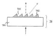
입사광과 회절광이 이루는 각도를 크게 취하여 광학 배치의 자유도를 높이기 위해서는 투과형 회절 격자를 사용하는 것이 바람직하다. 도 7 에 종래의 수지를 사용한 투과형 회절 격자의 일례를 나타낸다. 이 회절 소자는, 직선상의 톱니 형상 회절 격자를 정밀하게 형성한 도시하지 않은 금형을 투명 기판 (701) 인 유리 기판의 표면에 성막한 감광성 수지 (702) 에 압착하고 UV 광으로 경화 후, 이형함으로써 톱니 형상 회절 격자 (703) 를 형성하여, 투과형 톱니 형상의 회절 소 자 (70) 로 한 것이다.It is preferable to use a transmission diffraction grating in order to increase the degree of freedom of optical arrangement by taking the angle formed between the incident light and the diffracted light large. 7 shows an example of a transmission diffraction grating using a conventional resin. The diffraction element is obtained by pressing a mold (not shown) in which a linear sawtooth diffraction grating is precisely formed on the
또한, 도 8 에 톱니 형상이 계단에 근사한 투과형의 유사 톱니 형상 회절 격자의 일례를 나타낸다. 투명 기판 (801) 인 유리 기판의 표면에 포토리소그래피법과 에칭법을 반복하는 것으로 유사 톱니 형상 회절 격자 (802) 를 형성하고, 이 회절 격자를 투과형의 유사 톱니 형상의 회절 소자 (80) 로 한 것이다.8 shows an example of a transmission-like pseudo-tooth diffraction grating in which the sawtooth shape approximates a step. By repeating the photolithography method and etching method on the surface of the glass substrate which is the
여기서, 도 7 및 도 8 에서 실선의 화살표는 입사광이며, 일점 쇄선은 투과광이며, 파선은 - 1차 회절광을 각각 나타낸다.Here, in FIG. 7 and FIG. 8, the solid arrow is incident light, the dashed-dotted line is transmitted light, and the broken line represents-1st order diffracted light, respectively.
상기 기술한 종래예에서는, 투과형 톱니 형상의 회절 격자에서 높은 회절 효율을 얻기 위해서는, 격자 재료와 공기 등의 출사측 매질과의 굴절률 차와 격자의 깊이의 곱한 값으로 정의되는 위상 차를 파장 정도로 할 필요가 있다. 한편으로, 파장에 따른 분리의 각도를 크게 하기 위해서는 격자의 주기는 작을 수록 바람직하다. 이 때문에, 톱니 형상 회절 격자의 형상은 격자의 주기가 작고, 또한 격자의 깊이 (D) 의 격자의 주기 (T) 에 대한 비율로 정의되는 애스펙트비 (aspect ratio) (D/T) 가 큰 것이 필요하다.In the above-described conventional example, in order to obtain high diffraction efficiency in the transmission sawtooth diffraction grating, the phase difference defined by the product of the refractive index difference between the grating material and the emission medium such as air and the depth of the grating is about the wavelength. There is a need. On the other hand, in order to increase the angle of separation according to the wavelength, the smaller the period of the lattice, the better. For this reason, the shape of the sawtooth diffraction grating has a small period of the grating and a large aspect ratio (D / T) defined by the ratio of the grating depth D to the period T of the grating. need.
발명의 개시DISCLOSURE OF INVENTION
그러나, 애스펙트비가 큰 톱니 형상 회절 격자는 제작상의 곤란도가 높고, 수지를 사용하여 제작하기 위해서는, 금형 가공상의 제약이나 수지의 전사성/이형성 등의 문제를 가지고 있다. 이 때문에, 요구되는 파장에 따른 큰 분리 능력을 가져 높은 빛의 이용 효율을 갖는 회절 격자를 생산성이 좋고 저렴하게 얻을 수 없는 문제를 가지고 있었다.However, the sawtooth diffraction grating having a high aspect ratio has high manufacturing difficulty and has problems such as constraints in mold processing and transferability / release of resin in order to produce using resin. For this reason, there is a problem in that a diffraction grating having a large separation ability according to the required wavelength and having a high light utilization efficiency cannot be obtained with good productivity and low cost.
또한, 수지 재료를 사용하는 경우에는, 고온 하 및 고온 고습 하에서의 소자의 열화 등 신뢰성에서 문제를 가지고 있고, 한정된 환경 조건 하에서 밖에 소자를 사용할 수 없다는 문제를 가지고 있었다.Moreover, when using a resin material, it has a problem in reliability, such as deterioration of an element under high temperature and high temperature, high humidity, and has a problem that an element can be used only under limited environmental conditions.
한편, 유사 톱니 형상 회절 격자에 관해서는, 신뢰성 및 생산성에 뛰어나 저렴한 소자를 대량으로 생산할 수 있으나, 격자의 주기를 더욱 세분화한 가공을 실시하여 유사 톱니 형상 회절 격자로 할 필요가 있어, 주기가 작은 소자는 제작이 곤란하다는 문제를 가지고 있었다. 또한, 제작시의 오차에 의한 형상 변형이 크게 특성을 열화시켜 빛의 이용 효율이 높은 회절 격자를 수율 좋게 생산할 수 없다는 문제를 가지고 있었다.On the other hand, the quasi-toothed diffraction grating is excellent in reliability and productivity, and can be produced in large quantities inexpensive elements. However, it is necessary to perform a process in which the grating period is further refined to form a quasi-toothed diffraction grating. The device had a problem that manufacturing was difficult. In addition, there is a problem in that the shape deformation due to the error in manufacturing greatly degrades the characteristics, so that a diffraction grating having high light utilization efficiency cannot be produced with good yield.
어느 쪽의 종래 예에 대해서도, O 도 입사 (소자 표면으로의 수직 입사) 로 사용하는 경우에는, 격자의 주기가 파장의 약 2 배로 현저히 회절 효율이 저하하는 것이 알려져 있고, 높은 회절 효율과 소주기화 (약 2 배 등) 에 의한 빛의 파장에 따른 큰 분리의 양립이 곤란하다는 문제도 함께 가지고 있었다.In both conventional examples, when O is also used for incidence (vertical incidence to the element surface), it is known that the diffraction efficiency is remarkably lowered to about twice the wavelength of the grating period. It also had a problem that compatibility of large separation according to the wavelength of light by (about 2 times, etc.) was difficult.
본 발명은, 상기 기술한 실정을 감안하여 이루어진 것으로, 높은 빛의 이용 효율을 가지고, 또한 파장에 따른 분리가 크고, 광학계의 배치 자유도가 우수하며, 대량 생산에 알맞고, 또한 신뢰성 및 온도 특성이 우수한 회절 소자를 제공하는 것을 목적으로 한다.SUMMARY OF THE INVENTION The present invention has been made in view of the above-described circumstances, and has high light utilization efficiency, high separation according to wavelength, excellent degree of freedom of arrangement of optical system, suitable for mass production, and excellent in reliability and temperature characteristics. It is an object to provide a diffraction element.
본 발명은, 기판 표면에 형성된 또는 기판 상에 성막된 층에 형성된 격자이고, 단면이 요철 형상이고 볼록부 상면이 실질적으로 평탄하며 볼록부가 대칭인 격자를 갖는 회절 소자로서, 격자의 1 주기가 입사하는 빛의 파장과 실질적으로 같으며, 회절 소자의 격자 형성면에 빛이 경사져 입사하여 사용되는 것을 특징으로 하는 회절 소자를 제공한다.The present invention relates to a diffraction element having a grating formed on a surface of a substrate or formed on a layer deposited on a substrate, the grating having a concave-convex shape in cross section, a substantially flat upper surface of a convex portion, and a symmetrical convex portion, wherein one cycle of the grating is incident. It is substantially the same as the wavelength of light to provide a diffraction element, characterized in that the light is used to be inclined to the grating forming surface of the diffraction element.
또한, 상기 격자의 1 주기를 차지하는 볼록부와 오목부의 비율에서 볼록부의 비율이 오목부의 비율 이상인 상기의 회절 소자를 제공한다.Further, the above diffraction element is provided in which the ratio of the convex portion to the ratio of the convex portion to the concave portion occupying one period of the grating is equal to or greater than the ratio of the concave portion.
또한, 상기 격자의 볼록부를 형성하는 벽면이 경사지며, 1 주기를 차지하는 격자 볼록부의 상단의 비율이 격자 볼록부의 바닥부의 비율보다 작은 상기의 회절 소자를 제공한다.Furthermore, the wall surface which forms the convex part of the said grating | ramp is inclined, and the said diffraction element provided with said diffraction element whose ratio of the upper end of the grating convex part which occupies 1 period is smaller than the ratio of the bottom part of the grating convex part.
또한, 상기 회절 소자의 적어도 볼록부에, 이 볼록부와는 다른 1 층 이상의 광학 재료가 적층되어 이루어지는 상기의 회절 소자를 제공한다.Furthermore, the diffraction element mentioned above in which the optical material of one or more layers different from this convex part is laminated | stacked on at least the convex part of the said diffraction element is provided.
상기 광학 재료가 TiO2, SiO2, Ta2O5, Al2O3로부터 선택된 것으로 이루어지는 상기의 회절 소자를 제공한다.The diffractive element described above is provided wherein the optical material is selected from TiO2 , SiO2 , Ta2 O5 , Al2 O3 .
또한, 상기 기판으로서 투명 기판이 사용되고, 투명 기판 상에 성막된 층에 격자의 볼록부가 형성되며 격자의 볼록부는 투명 기판보다 굴절률이 높은 상기의 회절 소자를 제공한다.In addition, a transparent substrate is used as the substrate, a convex portion of the grating is formed in a layer formed on the transparent substrate, and the convex portion of the grating provides the above diffractive element having a higher refractive index than the transparent substrate.
투명 기판 상에 성막된 층이 SiO2, TiO2, Ta2O5, Si3N4, Si로 이루어지는 군으로부터 선택된 하나를 주성분으로 하는 층 또는 이들의 혼합물로 이루어지는 층인 상기의 회절 소자를 제공한다.Provided is the diffractive element described above, wherein the layer formed on the transparent substrate is a layer composed mainly of one selected from the group consisting of SiO2 , TiO2 , Ta2 O5 , Si3 N4 , and Si, or a mixture thereof. .
또한, 상기의 회절 소자의 하나의 면에 다른 광학 소자가 적층되어 일체화되어 있는 회절 소자를 제공한다.Further, a diffractive element in which another optical element is laminated and integrated on one surface of the diffractive element is provided.
또한, 기판 표면에 형성된 또는 기판 상에 성막된 층에 형성된 격자이고, 그 단면이 요철 형상이고 볼록부 상면이 실질적으로 평탄하며 볼록부가 대칭인 격자를 구비하며, 격자의 1 주기가 입사하는 빛의 파장과 실질적으로 같은 회절 소자의 사용 방법으로서, 회절 소자의 격자 형성면에 빛이 경사져 입사하여 사용되는 것을 특징으로 하는 회절 소자의 사용 방법을 제공한다.Also, a grating formed on the surface of the substrate or formed on a layer deposited on the substrate, the grating having a concave-convex shape, a substantially flat top surface of the convex portion, and a convex portion symmetrical, and having one cycle of the light incident As a method of using a diffraction element that is substantially the same as the wavelength, a method of using the diffraction element is characterized in that light is inclined and incident on the grating formation surface of the diffraction element.
또한, 상기 광이 경사져 입사할 때의 입사 각도가 회절 소자의 표면에 세운 법선에 대하여, 15° 내지 80°의 범위에 있는 상기의 회절 소자의 사용 방법을 제공한다.
또한, 상기의 회절 소자가 이용되고 있는 것을 특징으로 하는 광학 장치를 제공한다.The present invention also provides a method of using the diffractive element described above, wherein the angle of incidence when the light is inclined and enters is in the range of 15 ° to 80 ° with respect to the normal line placed on the surface of the diffraction element.
In addition, an optical device is provided, wherein the diffractive element is used.
또한, 상기의 광학 장치가 분광 장치이고, 상기 회절 소자의 기판으로서 투명 기판이 사용되고, 상기 회절 소자가 투과형 소자로서 사용되고 있는 것을 특징으로 하는 분광 장치를 제공한다.Furthermore, the optical device is a spectroscopic device, a transparent substrate is used as a substrate of the diffractive element, and the diffractive element is used as a transmission type element.
도 1 은 본 발명의 회절 소자의 구성의 일례를 나타내는 측면도이다.BRIEF DESCRIPTION OF THE DRAWINGS It is a side view which shows an example of a structure of the diffraction element of this invention.
도 2 는 본 발명의 회절 소자의 구성의 다른 예를 나타내는 측면도이다.2 is a side view showing another example of the configuration of the diffractive element of the present invention.
도 3 은 본 발명의 회절 소자의 구성의 별도의 예를 나타내는 측면도이다.3 is a side view illustrating another example of the configuration of the diffractive element of the present invention.
도 4 는 본 발명의 회절 소자에서의 볼록부에 다층막을 형성한 경우와 이렇게 하지 않은 경우 간의 회절 특성의 차이의 예를 나타내는 그래프이다.4 is a graph showing an example of the difference in diffraction characteristics between the case where a multilayer film is formed in the convex portion and the case where this is not done in the diffraction element of the present invention.
도 5 는 본 발명의 회절 소자에서의 입사 편광 방향의 차이에 의한 회절 특 성의 예를 나타내는 그래프이다.5 is a graph showing an example of diffraction characteristics by the difference in the incident polarization direction in the diffraction element of the present invention.
도 6 은 본 발명의 회절 소자에서의 오목부와 볼록부의 비율의 차이에 의한 회절 특성의 예를 나타내는 그래프이다.6 is a graph showing an example of diffraction characteristics due to a difference in the ratio of the concave portion and the convex portion in the diffraction element of the present invention.
도 7 은 종래의 회절 소자의 구성의 일례를 나타내는 측면도이다.7 is a side view showing an example of the configuration of a conventional diffractive element.
도 8 은 종래의 회절 소자의 구성의 다른 예를 나타내는 측면도이다.8 is a side view showing another example of the configuration of a conventional diffractive element.
도 9 는 본 발명의 회절 소자의 구성의 별도의 예를 나타내는 측면도이다.9 is a side view illustrating another example of the configuration of the diffractive element of the present invention.
도 10 은 본 발명의 회절 소자에서의 입사 편광 방향의 차이에 의한 회절 특성의 예를 도시하는 그래프이다.10 is a graph showing an example of diffraction characteristics due to a difference in incident polarization direction in the diffraction element of the present invention.
도 11 은 본 발명의 회절 소자의 구성의 별도의 예를 나타내는 측면도이다.11 is a side view illustrating another example of the configuration of the diffractive element of the present invention.
도 12 는 본 발명의 회절 소자의 구성의 다른 예를 나타내는 측면도이다.It is a side view which shows the other example of the structure of the diffraction element of this invention.
도 13 은 본 발명의 회절 소자에서의 격자 볼록부의 벽면의 테이퍼각의 변화에 의한 회절 특성의 예를 나타내는 그래프이다.It is a graph which shows the example of the diffraction characteristic by the change of the taper angle of the wall surface of the grating convex part in the diffraction element of this invention.
도 14 는 본 발명의 회절 소자에서의 격자 볼록부의 벽면의 테이퍼각의 변화에 의한 회절 특성의 별도의 예를 도시하는 그래프이다.It is a graph which shows the other example of the diffraction characteristic by the change of the taper angle of the wall surface of the grating convex part in the diffraction element of this invention.
발명을 실시하기Carrying out the invention 위한 최선의 형태 Best form for
본 발명은, 기판의 표면에 형성된 단면이 요철 형상이며 볼록부가 대칭인 격자가 형성된 회절 소자에 관한 것이고, 격자의 주기가 입사하는 빛의 파장과 같거나 또는 작은 것이다. 그리고, 빛이 격자 형성면에 대하여 경사져 입사하도록 하여 사용되는 회절 소자이다.The present invention relates to a diffraction element having a grating having a concave-convex shape and a convex portion symmetrical in cross section formed on the surface of a substrate, wherein the period of the grating is equal to or smaller than the wavelength of the incident light. And it is a diffraction element used so that light may incline with respect to a grating formation surface and it may be incident.
또한, 단면이 요철 형상인 격자는 기판 상에 성막된 층에 형성해도 된다. 기판 상에 성막하는 재료로서는 에칭 특성이 우수한 것이 바람직하고, SiO2, TiO2, Ta2O5, Si3N4, Si 등을 주성분으로 한 것이나 이들의 혼합막을 적용할 수 있다. 이러한 회절 소자의 구성으로 함으로써, 간이한 프로세스이면서 양산성이 우수하고, 높은 회절 효율이며 더구나 큰 파장 분리 효과를 갖는 회절 소자를 실현할 수 있다. 큰 파장 분리 효과를 갖기 때문에 분광용의 회절 격자로서 사용하는 것이 바람직하다.In addition, the grating having an uneven shape in cross section may be formed in a layer formed on a substrate. It is excellent in etching property preferable as the material for film formation on a substrate, whether by mainly ofSiO 2, TiO 2, Ta 2
여기서, 격자의 주기가 입사하는 빛의 파장과 실질적으로 같다는 것은 주기가 입사하는 파장의 ±45% 이내의 것을 말한다. 즉, 주기가 파장의 0.55~1.45배의 범위에 있다. 이 ±45% 이내이면, 입사 각도를 적절히 선택하는 것으로 특정한 회절광만이 발생한다는 점에서 본 발명의 효과를 손상하지 않는다. 또한, 빛이 격자 형성면에 대하여 경사져 입사한다는 것은, 소자의 표면에 세운 법선에 대하여 15° 내지 80°까지의 각도를 말하고, 특히 25° 내지 65°까지의 경우는 본 발명의 효과를 충분히 달성할 수 있다.Here, that the period of the grating is substantially the same as the wavelength of the incident light means that the period is within ± 45% of the incident wavelength. In other words, the period is in the range of 0.55 to 1.45 times the wavelength. If it is within +/- 45%, the effect of this invention is not impaired in that only specific diffraction light generate | occur | produces by selecting an incidence angle suitably. Incidentally, incidence of light inclined with respect to the lattice forming surface means an angle of 15 ° to 80 ° with respect to the normal line placed on the surface of the device, and particularly in the case of 25 ° to 65 °, the effect of the present invention is sufficiently achieved. can do.
회절 격자의 요철부에서의 대칭인 볼록부의 단면 형상은, 구형 (rectangular), 사다리꼴 등이면 되고, 이 어느 쪽이더라도 본 발명에서의 효과를 갖지만, 구형에 가까운 것이 제작상 바람직하다.The cross-sectional shape of the convex portions that are symmetrical in the uneven portions of the diffraction grating may be rectangular, trapezoidal, or the like, and any one of these effects has the effect of the present invention, but it is preferable in production to be close to the spherical shape.
회절 소자에 사용되는 기판은, 투명 기판으로는, 석영 유리, 유리, 규소, 폴리카보네이트 등의 기판을 사용할 수 있다. 이들의 중에서, 석영 유리, 유리의 기판이 내구성 등의 관점에서 바람직하다. 또한, 반사형 회절 소자로 구성하는 경우에는, 회절 격자상에 금속이나 다층막으로 이루어지는 반사코팅을 실시하는 것이 바람직하고, 상기 기술한 투명 기판에 더하여 불투명한 기판인, 예를 들어, 결정화 유리나 세라믹스 등을 사용할 수도 있다.As a board | substrate used for a diffraction element, board | substrates, such as quartz glass, glass, silicon, a polycarbonate, can be used as a transparent substrate. Among these, quartz glass and a substrate of glass are preferable from the viewpoint of durability. In the case of a reflective diffraction element, it is preferable to perform a reflection coating made of a metal or a multilayer film on the diffraction grating, and in addition to the above-mentioned transparent substrate, it is an opaque substrate, for example, crystallized glass or ceramics. You can also use
이하에서는, 볼록부의 형상이 구형이라고 하여, 본 발명을 도면을 참조로 하면서 설명한다.Hereinafter, the convex portion will be described as having a spherical shape with reference to the drawings.
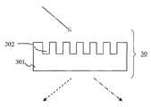
도 3 은 본 발명의 투과형의 회절 소자의 구성의 일례를 나타내는 측면도이다. 투명 기판 (301) 상에, 격자의 주기가 입사하는 빛의 파장보다도 작은 구형 회절 격자 (302) 가 포토리소그래피 및 건식 에칭의 수법에 의해 형성되어 회절 소자 (30) 를 이루고 있다. 격자의 주기가 P에서 주어지는 회절 격자 (정확히는 그 길이 방향) 에 대하여, 법선 방향과 이루는 각도 (i) 로 입사한 파장 (λ) 의 빛은, (식 1) 에서 정의되는 회절 각도 θ 의 방향에서 m 차 회절광을 발생한다. (식 1) 에서 명백히 한 바와 같이, 회절 격자 (302) 에 대하여 수직으로 입사한 경우에는 파장보다도 작은 주기의 회절 격자의 회절광은 존재할 수 없다. 그러나, 유한한 각도를 가지고, 즉, 경사 방향으로부터 빛을 입사했을 때에는, 파장보다도 주기가 작은 경우에도 차수를 갖는 회절광이 존재할 수 있다. 이 때문에, 구조상 볼록부가 대칭인 형상을 가지고 있더라도, 비대칭인 회절 특성을 나타내는 것을 알 수 있다.3 is a side view showing an example of the configuration of a transmission diffraction element of the present invention. On the
sin(θ) + sin(i) = m?λ/P … (식 1)sin (θ) + sin (i) = m? λ / P... (Equation 1)
이 경사 입사에 의한 효과를 이용함으로써, 제작이 용이한 대칭으로 구형상의 회절 격자라도, 충분히 높은 회절 효율과 큰 회절 각도를 얻을 수 있다. 일례로서, 격자의 주기가 1000nm (오목부와 볼록부의 폭이 각각 500nm) 이고, 깊이가 약 2300nm 인 회절 격자에 법선에 대하여 약 50 도의 각도로 입사한 경우의 계산에 의한 - 1차 회절 효율의 파장 의존성을 도 4 에서 검은 원을 실선으로 이어서 나타낸다. 격자에 평행하게 편광한 직선 편광의 입사광에 대하여, 격자의 주기보다도 긴 1520nm 에서 1620nm 의 범위에서, - 1차 회절에 광량이 집중하여 높은 회절 효율을 나타내고 있는 것을 알 수 있다.By utilizing the effect of the oblique incidence, a sufficiently high diffraction efficiency and a large diffraction angle can be obtained even in a symmetrical spherical diffraction grating which is easy to manufacture. As an example, the first-order diffraction efficiency is calculated by the calculation when the grating period is 1000 nm (500 nm width of the concave portion and the convex portion, respectively 500 nm), and the diffraction grating has a depth of about 2300 nm at an angle of about 50 degrees with respect to the normal line. The wavelength dependence is shown by the solid circles in FIG. 4 in solid lines. It can be seen that, for the incident light of linearly polarized light polarized parallel to the grating, in the range of 1520 nm to 1620 nm longer than the period of the grating, the amount of light is concentrated in the first-order diffraction, indicating high diffraction efficiency.
더욱이, 회절 효율을 향상시켜 파장 의존성을 저감시키기 위해서는 격자의 볼록부상에 적절한 다층 구조를 부여하는 것이 효과가 있다. 일례로서 TiO2 를 고굴절률 재료로 하고, SiO2 를 저굴절률 재료로서 사용한 4 층막을 격자의 볼록부의 상부에 형성하였을 때의 회절 효율의 파장 의존성을 도 4 에 흰 원을 파선으로 이어서 나타낸다. 도 4 에서 명백히 한 바와 같이, 전파장 영역에서 한결같이 높은 회절 효율이 얻어지고 있는 것을 알 수 있다.Moreover, in order to improve the diffraction efficiency and to reduce the wavelength dependency, it is effective to give an appropriate multilayer structure on the convex portion of the grating. As an example, the wavelength dependence of the diffraction efficiency when a four-layer film using TiO2 as a high refractive index material and SiO2 as a low refractive index material is formed on the convex portion of the lattice is shown in FIG. As apparent from FIG. 4, it can be seen that a consistently high diffraction efficiency is obtained in the full-wavelength region.
즉, 회절 소자의 볼록부에, 볼록부와는 다른 1 층 이상의 광학 재료가 적층되어 있는 것이 회절 효율을 향상시킬 수 있어 바람직하다. 광학 재료란, 상기 TiO2, SiO2 이외에 Ta2O5, Al2O3 등을 들 수 있다.That is, it is preferable that the one or more layers of optical materials different from the convex part are laminated | stacked on the convex part of a diffraction element since it can improve diffraction efficiency. Examples of the optical material include Ta2 O5 , Al2 O3 , and the like, in addition to TiO2 and SiO2 .
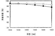
다른 예로서, 격자의 주기가 1500nm 이고, 깊이가 약 3000nm 인 회절 격자에 약 30 도의 각도로 입사한 경우의 회절 효율의 파장 의존성을 도 5 에 나타낸다. 도 5 의 곡선에서 검은 원을 실선으로 이은 것은 격자에 평행하게 편광한 직선 편광에 대한 회절 효율을 나타내고, 흰 원을 파선으로 이은 것은 격자에 수직으로 편 광한 직선 편광의 회절 효율을 나타낸다. 도 5 에서 명백히 한 바와 같이, 어느쪽의 편광에 대해서도 높은 회절 효율을 나타내고 있다.As another example, the wavelength dependence of the diffraction efficiency when the grating period is 1500 nm and is incident at an angle of about 30 degrees to a diffraction grating having a depth of about 3000 nm is shown in FIG. 5. In the curve of FIG. 5, the black circle with solid line represents the diffraction efficiency for linearly polarized light polarized parallel to the grating, and the white circle with broken line represents diffraction efficiency of linearly polarized light polarized perpendicular to the grating. As apparent from Fig. 5, high diffraction efficiency is shown for both polarizations.
이 도 5 에 나타내는 예에서는, 직교하는 직선 편광의 어느 것에 대해서도 높은 회절 효율이 얻어지고 있으나, 단파장 영역의 1520nm 및 장파장 영역의 1620nm 에 근접해짐에 따라서 회절 효율의 차가 커지는 경향이 있다. 이 차를 작게 하기 위해서는 격자를 형성하는 볼록부와 오목부의 비율을 조정함으로써 효과가 있다. 도 6 에, 격자의 1 주기를 차지하는 볼록부의 각각의 비율에 대하여 깊이를 최적화시킨 회절 격자의 파장 1520nm 에서 1620nm 까지의 범위에서의 직교하는 두 개의 편광에 의한 회절 효율의 차를 나타낸다. 도 6 에서 명백히 한 바와 같이, 직교하는 두 개의 편광에서의 회절 효율의 차는, 볼록부가 차지하는 비율이 반보다도 커진 경우에 현저히 억제된다. 이와 같이 격자 내의 볼록부의 1 주기를 차지하는 비율을 조정함으로써 입사 편광 의존성이 적은 회절 격자로 할 수도 있다.In the example shown in FIG. 5, high diffraction efficiency is obtained for any of the orthogonal linearly polarized light, but the difference in diffraction efficiency tends to increase as it approaches 1520 nm in the short wavelength region and 1620 nm in the long wavelength region. In order to make this difference small, it is effective by adjusting the ratio of the convex part and recessed part which form a grating | lattice. 6 shows the difference in diffraction efficiency due to two orthogonal polarizations in the wavelength range from 1520 nm to 1620 nm of the diffraction grating whose depth is optimized for each ratio of the convex portions occupying one period of the grating. As is apparent from FIG. 6, the difference in diffraction efficiency in two orthogonal polarizations is significantly suppressed when the ratio of the convex portion occupies more than half. Thus, by adjusting the ratio which occupies one period of the convex part in a grating | lattice, it can also be set as the diffraction grating with little incident polarization dependence.
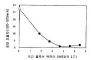
직교하는 직선 편광에 대한 회절 효율의 차를 작게 하기 위해서는, 격자 상단의 볼록부와 오목부의 비율을 약 1 로 유지한 뒤에, 격자 볼록부 벽면의 기판 표면의 수직선에 대한 각도 (이하, 테이퍼각이라고 한다) 를 조정함으로써도 효과가 있다. 도 13 에, 도 6 과 같이 석영 유리 기판의 표면에 형성한 격자 주기 1500nm 에서 깊이 3600nm 의 회절 격자의 파장 1520nm 에서 1570nm 까지의 범위에서의 직교하는 두 개의 편광에 대한 회절 효율의 차를 나타낸다.In order to reduce the difference in diffraction efficiency with respect to orthogonal linearly polarized light, after maintaining the ratio of the convex portion and the concave portion at the upper end of the lattice at about 1, the angle to the vertical line of the substrate surface of the lattice convex wall surface (hereinafter referred to as taper angle) Is also effective. FIG. 13 shows the difference in diffraction efficiency with respect to two orthogonal polarized light in the wavelength range of 1520 nm to 1570 nm of a diffraction grating having a depth of 3600 nm and a grating period 1500 nm formed on the surface of the quartz glass substrate as shown in FIG. 6.
도 13 에서 명백히 한 바와 같이, 직교하는 두 개의 편광에서의 회절 효율의 차는, 상기 기술한 테이퍼각에 의해 변화하여 3 도 이상의 테이퍼각, 바람직하게는 약 4 도의 테이퍼각으로 함으로써 현저히 개선된다. 이와 같이, 격자 측벽의 테이퍼각을 조정함으로써 입사 편광 의존성이 적은 회절 격자로 할 수도 있다.As is apparent from Fig. 13, the difference in diffraction efficiency at two orthogonal polarizations is remarkably improved by changing the taper angle described above to a taper angle of 3 degrees or more, preferably a taper angle of about 4 degrees. In this way, by adjusting the taper angle of the grating sidewalls, the diffraction grating can have a low incident polarization dependency.
이들의 조정으로 편광 의존성을 억제함으로써, 격자 깊이에 의한 회절 특성의 격차도 억제되기 때문에 제작시의 수율이 높아지는 효과도 더불어 갖는다.By suppressing the polarization dependence by these adjustments, the difference in diffraction characteristics due to the grating depth is also suppressed, which also has the effect of increasing the yield at the time of manufacture.
즉, 회절 격자의 1 주기를 차지하는 볼록부와 오목부와의 비율에 있어서 볼록부의 비율이 오목부의 비율 이상, 즉 0.5 이상이도록 하면, 직교하는 두 개의 편광에 의한 회절 효율의 차를 작게 할 수 있기 때문에 바람직하다. 또한, 회절 격자의 볼록부를 형성하는 벽면이 경사지고, 1 주기를 차지하는 격자 상단의 볼록부의 비율이 격자 바닥부의 볼록부의 비율보다 작도록 하면, 직교하는 두 개의 편광에 의한 회절 효율의 차를 작게 할 수 있기 때문에 바람직하다.In other words, if the ratio of the convex portion is equal to or greater than the ratio of the concave portion in the ratio between the convex portion and the concave portion occupying one period of the diffraction grating, the difference in diffraction efficiency due to the two orthogonal polarizations can be reduced. It is preferable because of that. Further, if the wall surface forming the convex portion of the diffraction grating is inclined, and the ratio of the convex portion at the top of the grating occupying one period is smaller than the ratio of the convex portion at the bottom of the grating, the difference in diffraction efficiency due to two orthogonal polarizations can be reduced. It is preferable because it can.
또한, 회절 격자의 주기를 작게 함으로써 파장에 대한 분리 각도의 변화를 크게 하는 것이 파장 분해능을 향상시키기 위해서는 효과가 있지만, 격자의 주기를 상기 기술한 예와 같이 1500nm 에서 1000nm 까지 작게 한 경우에는, 입사하는 편광 방향에 의한 회절 효율의 차는 현저해지는 경향에 있다.In addition, increasing the change in separation angle with respect to the wavelength by decreasing the period of the diffraction grating is effective to improve the wavelength resolution. However, when the period of the grating is reduced from 1500 nm to 1000 nm as in the example described above, The difference in diffraction efficiency due to the polarization direction is inclined to become remarkable.
이 때문에, 격자 볼록부의 격자의 주기를 차지하는 비율을 조정하더라도, 일정한 효과는 볼 수 있지만 충분하지 않다. 격자의 주기가 1OOOnm 인 경우에 입사하는 편광 방향에 의한 회절 효율의 차를 저감하기 위해서는, 격자 볼록부를 구성하는 재료로서 투명 기판 상에 성막된 투명 기판보다도 고굴절률의 재료를 사용함으로써 효과가 있다.For this reason, even if the ratio which occupies the period of the grating | lattice of a grating convex part is adjusted, although a certain effect can be seen, it is not enough. In order to reduce the difference in diffraction efficiency due to the polarization direction incident when the period of the grating is 100 ONm, it is effective to use a material having a higher refractive index than the transparent substrate formed on the transparent substrate as the material constituting the grating convex portion.
도 10 에, 입사하는 각종의 편광 방향에 대한 회절 효율의 파장 의존성을 나타낸다. 석영 유리 기판 상에 격자 볼록부와 오목부의 비율을 같게 가공한 경우의 특성을 흰 원으로 나타낸다. 도 10 의 곡선에서 흰 원을 실선으로 이은 것 및 곡선에서 흰 원을 점선으로 이은 것은, 각각 격자 방향에 대하여, 즉 격자의 길이 방향에 대하여 평행 및 수직으로 편광한 빛에 대한 특성을 나타낸다.10 shows wavelength dependence of diffraction efficiency with respect to various incident polarization directions. The characteristic at the time of processing the ratio of a lattice convex part and a recessed part on the quartz glass substrate equally is shown by a white circle. A solid circle of white circles in the curve of FIG. 10 and a dashed circle of white circles in the curve show characteristics of light polarized parallel and vertically with respect to the lattice direction, that is, with respect to the longitudinal direction of the lattice, respectively.
한편, 도 10 에서, 투명 기판 상에 성막된 굴절률이 약 2 인 재료를 갖는 격자 볼록부로 한 경우의 특성을 검은 원으로 나타낸다. 도 10 의 곡선에서 검은 원을 실선으로 이은 것 및 곡선에서 검은 원을 점선으로 이은 것은, 격자 방향에 대하여 각각 평행 및 수직으로 편광한 빛에 대한 특성을 나타낸다. 도 10 에서 명백히 한 바와 같이, 입사하는 편광 방향에 대한 회절 효율의 차가 저감하고 있는 것을 알 수 있다.On the other hand, in FIG. 10, the characteristic at the time of making the lattice convex part which has the material whose refractive index formed on the transparent substrate about 2 is shown by the black circle | round | yen. The solid circle of the black circle in the curve of FIG. 10 and the dotted line of the black circle in the curve represent the characteristics of light polarized in parallel and perpendicular to the lattice direction, respectively. As apparent from FIG. 10, it can be seen that the difference in diffraction efficiency with respect to the incident polarization direction is reduced.
도 13 에 나타낸 상기 기술한 예와 같이, 투명 기판 상에 성막된 굴절률이 약 2 의 재료를 갖는 격자 볼록부로 한 경우에도, 격자 상단의 볼록부와 오목부의 비율을 약 1 로 유지한 채로 격자 볼록부의 테이퍼각을 조정함으로써, 편광 방향에 대한 회절 효율의 차를 저감하는 것이 가능하다. 도 14 는, 투명 기판 상에 성막된 굴절률이 약 2 의 재료를 갖는 격자 볼록부로 한 회절 격자의 파장 1520nm 에서 1570nm 까지의 범위에서의 직교하는 편광 방향의 두 개의 편광에 대한 회절 효율의 차를 나타낸다. 도 14 에서 굴절률이 약 2 의 재료를 갖는 격자 볼록부로 한 경우에도, 약 6 도의 테이퍼각으로 함으로써 직교하는 편광 방향의 두 개의 편광에서의 회절 효율의 차는 현저히 개선되는 것이 명백하다.As in the above-described example shown in FIG. 13, even when the refractive index formed on the transparent substrate is a lattice convex part having a material of about 2, the lattice convex is maintained while maintaining the ratio of the convex portion and the concave portion at the upper end of the lattice to about 1. By adjusting the negative taper angle, it is possible to reduce the difference in diffraction efficiency with respect to the polarization direction. FIG. 14 shows the difference in diffraction efficiency for two polarizations in the orthogonal polarization direction in the range from 1520 nm to 1570 nm in wavelength of a diffraction grating having a refractive index deposited on a transparent substrate as a lattice convex having a material of about 2; . Even in the case where a lattice convex portion having a refractive index of about 2 is used in FIG. 14, it is evident that the difference in diffraction efficiency in two polarizations in orthogonal polarization directions is remarkably improved by having a taper angle of about 6 degrees.
또한, 상기의 모든 예로부터, 입사광선과 회절광이 투과형의 회절 격자면에 대하여 거의 거울 상(像)의 관계, 즉 입사 각도와 회절 각도가 거의 같은 경우에 높은 회절 효율을 얻을 수 있는 것을 알 수 있다. 이 배치는 반사형의 회절 격자에서 리트로우 (Littrow) 배치라고 불리우는, 입사광선과 회절광이 겹치는 배치의 투과형의 회절 격자의 경우의 배치라고 할 수 있다.In addition, from all the above examples, it is understood that high diffraction efficiency can be obtained when the incident light and the diffracted light have a substantially mirror image relationship with respect to the transmissive diffraction grating plane, that is, when the incident angle and the diffraction angle are substantially the same. Can be. This arrangement can be said to be an arrangement in the case of a transmissive diffraction grating of the arrangement in which the incident light and the diffracted light overlap, called the litrow arrangement in the reflective diffraction grating.
또한, 일반적으로는 광학 부품에 대하여, 계면 반사를 저감하기 위한 광학 다층막에 의한 코팅이 실시되지만, 상기의 예와 같이 애스펙트비가 큰 회절 격자의 경우에는 오목부와 볼록부에서의 성막 특성이 다르기 때문에 형상이 열화하는 등의 폐해가 많고, 결과적으로는 빛의 이용 효율을 저하시키는 경우가 많다. 미리 저반사 코팅을 실시한 기판 상에 회절 격자를 제작함으로써, 투과율을 향상시킬 수 있다. 이 때는, 격자 측부 및 바닥부에는 저반사 코팅은 실시되어 있지 않지만, 격자 형상의 열화는 없고 격자 상부에만 저반사 코팅이 실시된다.In general, the optical component is coated with an optical multilayer film for reducing interfacial reflection. However, in the case of a diffraction grating having a large aspect ratio as in the above example, the film formation characteristics at the concave and convex portions are different. There are many disadvantages such as deterioration of the shape, and as a result, the utilization efficiency of light is often lowered. The transmittance can be improved by producing a diffraction grating on a substrate to which the low reflection coating has been previously applied. At this time, the low reflection coating is not applied to the lattice side and the bottom, but the lattice shape is not deteriorated, and the low reflection coating is applied only to the upper part of the lattice.
본 발명의 구성을 사용함으로써, 간편한 가공 프로세스로 큰 파장 분리 효과를 가지고, 또한 높은 빛의 이용 효율을 얻을 수 있는 분광 회절 격자를 입사광과 회절광의 분리를 충분히 취한 투과형의 회절 격자에 의해 실현할 수 있다. 이 구성에 의해, 신뢰성, 양산성 등이 우수한 분광 회절 소자를 실현할 수 있고, 더욱 저렴한 분광 시스템을 실현할 수 있다. 또한, 투과 배치에서 사용할 수 있기 때문에 분광 시스템의 설계에 큰 자유도를 가지고 있다.By using the configuration of the present invention, a spectral diffraction grating having a large wavelength separation effect and a high light utilization efficiency can be realized by a transmission diffraction grating sufficiently separating incident light and diffracted light with a simple processing process. . By this structure, the spectral diffraction element which is excellent in reliability, mass productivity, etc. can be realized, and a cheaper spectral system can be realized. It also has great freedom in the design of spectroscopic systems because it can be used in transmission arrangements.
본 발명의 회절 소자에서의 회절 격자 패턴은, 포토마스크 등을 사용하여 제작할 수 있기 때문에, 회절 격자 패턴은 직선 형상에 한정되지 않고, 예를 들어 곡선 형상으로 할 수도 있다. 이 곡선 형상으로 하는 것에 의해, 회절광이 광검출기 상에서 집광하도록 렌즈 기능을 부가할 수도 있다. 또한, 대면적의 웨이퍼프로세스를 사용함으로써, 위상판 등 다른 기능을 갖는 광학 소자를 회절 소자에 적층할 수 있어, 한층 더 고기능화, 복합화 등을 실시할 수 있다.Since the diffraction grating pattern in the diffraction element of this invention can be produced using a photomask etc., a diffraction grating pattern is not limited to a linear shape, For example, it can also be made into a curved shape. By setting it as a curved shape, a lens function can be added so that diffracted light may collect on a photodetector. In addition, by using a large-area wafer process, optical elements having other functions, such as a phase plate, can be laminated on the diffraction element, and further higher functionalization and complexation can be performed.
적층하는 다른 광학 소자로서는, 개구 제한, 수차 보정, 렌즈 효과, 빔 정형, 편광 변환, 위상 조정, 강도 조정 등의 기능을 갖는 광학 소자를 들 수 있다. 적층하는 광학 소자는, 회절 소자, 액정 소자, 다층막 소자 등의 대면적의 웨이퍼프로세스를 적용할 수 있는 것이 바람직하다.As another optical element to laminate | stack, the optical element which has functions, such as aperture restriction, aberration correction, lens effect, beam shaping, polarization conversion, phase adjustment, intensity adjustment, is mentioned. It is preferable that a large area wafer process, such as a diffraction element, a liquid crystal element, and a multilayer film element, can be applied to the optical element to laminate | stack.
즉, 상기의 회절 소자의 하나의 면에, 다른 광학 소자가 적층되어 일체화되어 있는 것이, 회절 소자에 다른 광학적 기능을 부가하여 고기능화할 수 있어 바람직하다.That is, it is preferable that another optical element is laminated and integrated on one surface of the diffraction element because it can add another optical function to the diffraction element and make it highly functionalized.
본 발명에서의 회절 격자는, 기판인, 예를 들어 유리 기판 그 자체 또는 유리 기판 상에 성막된 무기물 재료를 가공하여 제작된다. 특히, 성막의 공정을 생략할 수 있어, 성막과 기판의 계면이 존재하지 않는 점에서 유리 기판에 직접 격자를 형성하는 것이 바람직하다. 즉, 고속이고 또한 균일한 에칭 특성을 갖는 석영계의 유리 기판을 직접 가공하는 것이 매우 바람직하고, 더욱이 신뢰성, 양산성 등의 점에서도 석영계의 유리 기판이 바람직하다.The diffraction grating in this invention is produced by processing the inorganic material formed into a film, for example on the glass substrate itself or a glass substrate. In particular, it is preferable to form a lattice directly on the glass substrate because the step of film formation can be omitted and the interface between the film formation and the substrate does not exist. That is, it is very preferable to directly process a quartz glass substrate which has a high speed and uniform etching characteristic, and a quartz glass substrate is also preferable from the point of reliability, mass productivity, etc.
또한, 온도 변화에 의한 회절 방향의 변화를 억제하기 위해서는, 사용하는 기판의 선팽창 계수의 제어가 중요하고, 선팽창 계수를 최적화한 투명 기판을 사용하는 것이 온도 특성이 뛰어난 소자를 얻기 위해서 바람직하다. 이 경우, 선팽 창 계수를 최적화한 투명 기판의 표면에 직접 가공을 실시해도 되고, 에칭 특성이 우수한 무기물 재료를 선팽창 계수를 최적화한 투명 기판 상에 성막하여 가공층으로 할 수도 있다.Moreover, in order to suppress the change of the diffraction direction by temperature change, control of the linear expansion coefficient of the board | substrate used is important, and it is preferable to use the transparent substrate which optimized the linear expansion coefficient in order to obtain the element excellent in temperature characteristic. In this case, you may process directly to the surface of the transparent substrate which optimized the linear expansion coefficient, and the inorganic material which is excellent in etching characteristic may be formed into a processed layer by forming into a film on the transparent substrate which optimized the linear expansion coefficient.
일례로서 선팽창 계수를 억제한 유리 기판재료로서는, Ti를 도핑한 석영 유리나 Al2O3-LiO3-SiO2 등을 주성분으로 하는 유리 등을 사용할 수 있지만, 프로세스 중의 기판 온도 이력에 의한 영향이 적고, 또한 에칭성이 우수한 Ti를 도핑한 석영 유리가 직접 기판 가공하기 위해서는 특히 바람직하다.As an example, as the glass substrate material which suppressed the coefficient of linear expansion, quartz doped with Ti, glass mainly composed of Al2 O3 -LiO3 -SiO2, or the like can be used, but the influence of the substrate temperature history in the process is small. In addition, quartz glass doped with Ti having excellent etching properties is particularly preferable for direct substrate processing.
또한, 상기의 예와 같은 애스펙트비가 큰 격자의 형성시에는 소자 외주부는 미가공으로 하는 것이, 가공 중의 포토레지스트마스크나 격자 재료의 파손을 막는데에서 바람직하다.In the formation of a lattice having a large aspect ratio as in the above example, it is preferable that the outer peripheral portion of the element be unprocessed in order to prevent damage to the photoresist mask or lattice material during processing.
본 발명의 회절 소자가 회절 각도를 특히 크게 함으로써 파장 분해능을 향상시키는 주기가 작은 회절 격자이면 그 효과가 현저하고, 특히 회절 격자의 주기가 중심 파장과 거의 같은 것, 또는 주기 (피치) 가 중심 파장에 비해 작은 범위에 있는 것에서는 효과가 크다.If the diffraction grating of the present invention has a diffraction grating having a small period of improving the wavelength resolution by increasing the diffraction angle particularly large, the effect is remarkable. In particular, the period of the diffraction grating is almost equal to the center wavelength, or the period (pitch) is the center wavelength. In the small range compared to the effect is great.
상기의 본 발명의 회절 소자를 사용하여 각종의 광학 장치가 구성된다. 이 광학 장치는 본 발명의 회절 소자의 분광 특성 등의 특성을 사용한 것이면, 어느 광학 장치여도 된다.Various optical devices are configured using the diffraction element of the present invention described above. As long as this optical apparatus uses characteristics, such as the spectral characteristics of the diffraction element of this invention, any optical apparatus may be sufficient.
또한, 상기의 회절 소자의 기판으로서 투명 기판이 사용되고, 회절 소자가 투과형 소자로서 사용되어 분광 장치가 구성되는 것이, 본 발명의 회절 소자는 큰 파장 분리 효과를 가지며, 입사광과 투과 회절광의 분리 각도를 크게 얻을 수 있기 때문에, 배치 상의 제약이 없어 바람직하다.In addition, a transparent substrate is used as a substrate of the diffraction element, and a diffraction element is used as a transmission element, so that a spectrometer is constructed. The diffraction element of the present invention has a large wavelength separation effect, and the separation angle between incident light and transmitted diffraction light is increased. Since it can obtain large, there is no restriction | limiting in arrangement, and it is preferable.
본 발명의 분광 장치란, 예를 들어 광통신으로 사용되는 파장 다중 통신의 검출기가 있다. 1520nm 에서 1620nm 까지의 다른 파장의 신호광이 동일한 전송 화이버에 의해 전파해 온 경우에, 각 파장에 분파하여 각각의 신호 강도를 측정할 필요가 있다. 전송 화이버로부터 출사한 빛은, 본 발명의 회절 소자에 의해 파장에 따라 다른 방향으로 회절?전파하고, 다른 수광 소자에 입사함으로써 각 파장의 신호 강도를 측정할 수 있다. 게다가, 파장에 따라 전파 경로가 다르기 때문에 각각의 파장에 대하여 다른 강도나 위상의 조정을 실시하는 것도 가능하다. 반사형의 소자를 사용하는 경우에는 높은 빛의 이용 효율을 얻기 위해서는, 입사광과 반사 회절광이 가까운 리트로우 배치라고 불리우는 배치가 일반적이고, 입사 화이버와 검출기의 배치에 제약이 생기지만, 본 발명의 투과형의 회절 소자는 반사 리트로우 배치와 동등한, 높은 빛의 이용 효율을 실현하면서도 입사광과 회절광이 이루는 각도가 크고 배치상의 제약이 적은 점에서 우수하다.The spectrometer of the present invention is, for example, a detector of wavelength multiplexing communication used in optical communication. When signal light of different wavelengths from 1520 nm to 1620 nm has been propagated by the same transmission fiber, it is necessary to offset each wavelength and measure the respective signal strengths. The light emitted from the transmission fiber is diffracted and propagated in different directions depending on the wavelength by the diffraction element of the present invention, and the signal intensity at each wavelength can be measured by entering the other light receiving element. In addition, since the propagation path is different depending on the wavelength, it is also possible to adjust different intensities or phases for each wavelength. In the case of using a reflective element, in order to obtain high light utilization efficiency, an arrangement called a reflow arrangement in which incident light and reflected diffracted light are close is common, and the arrangement of the incident fibers and the detector is restricted. The transmissive diffraction element is excellent in that the angle between the incident light and the diffracted light is large and the arrangement constraint is small while realizing a high light utilization efficiency equivalent to the reflective retrow arrangement.
이하에, 실시예를 나타낸다.An example is shown below.
[예 1][Example 1]
도 1 은, 본 예의 분광 회절 소자의 구성을 나타내는 측면도이다. 본 예에서는, 두께 2.0mm 의 석영 유리 기판을 투명 기판 (101) 으로 하고, 투명 기판의 한 면에 TiO2 및 SiO2 를 사용한 5O 도의 입사 각도에 대하여 가장 반사율이 낮은 4 층의 반사 방지막 (102) 을 사용하였다. 그 후, 포토리소그래피 및 건식 에칭의 기술을 사용하여 구형상의 회절 격자를 형성하였다. 즉, 먼저, 격자의 오목부에 대응하는 반사 방지막 부분을 에칭에 의해 제거한 후에, 석영 유리의 가공 깊이가 900nm 인 에칭을 실시하고, 석영 유리의 볼록부의 위에 다층막이 형성된 격자의 주기가 1000nm 인 구형 회절 격자 (103) 를 형성하였다. 오목부와 볼록부의 폭의 비는 1:1 이었다.1 is a side view showing the configuration of a spectral diffraction element of this example. In this example, a quartz glass substrate having a thickness of 2.0 mm is used as the
다음으로, 투명 기판 (101) 의 구형 회절 격자 (103) 를 형성한 면과는 반대측의 면에 상기와 같이 50 도의 입사광에 대한 4 층의 반사 방지막 (104) 을 사용하였다. 그 후, 다이싱소 (dicing saw) 에 의해 투명 기판 (101) 을 15mm × 10mm 의 장방형으로 절단하여 회절 소자 (10) 로 하였다.Next, four layers of
회절 소자 (10) 의 구형 회절 격자 (103) 측에서, 격자에 대하여 평행하게 편광한 파장 1520nm, 1570nm 및 1620nm 의 빛을 외부 입사각 50°로 입사한 바, 각 파장에 대하여 각각 92%, 93% 및 91% 의 높은 회절 효율을 나타내었다. 또한, 입사하는 빛의 파장에 의해 회절광의 출사 방향은 각각 49 도, 54 도 및 59 도로 변화하여, 3 개의 파장의 빛을 충분히 분리할 수 있었다. 도 1 에서, 실선의 화살표는 입사광, 일점 쇄선은 투과광, 파선은 - 1차 회절광을 각각 나타낸다.On the
[예 2][Example 2]
도 2 는, 본 예의 분광 회절 소자의 구성을 나타내는 측면도이다. 본 예에서는, 두께 2.0mm 의 석영 유리 기판을 투명 기판 (201) 으로 하였다. 투명 기판 (201) 상에 포토레지스트를 도포하고, 개구부가 격자의 주기의 1/3 이 되는 도시하지 않은 포토마스크를 사용하여 포토리소그래피법을 사용하여, 볼록부와 오목부의 폭의 비율이 2:1 인 포토레지스트마스크를 형성하였다. 그 후, 건식 에칭의 기술을 사용하여 깊이 3400nm 의 구형 회절 격자를 형성하였다. 즉, 격자의 주기가 1500nm 이고, 격자는 1000nm 폭의 볼록부와 500nm 폭의 오목부로 이루어지며, 석영 유리의 가공 깊이가 3600nm 인 구형 회절 격자 (202) 를 형성하였다.2 is a side view showing the configuration of the spectral diffraction element of this example. In this example, the quartz glass substrate having a thickness of 2.0 mm was used as the
다음으로, 투명 기판 (201) 의 구형 회절 격자 (202) 를 형성한 면과는 반대측의 면에 30 도의 입사광에 대한 반사 방지막 (203) 을 시설하였다. 그 후, 다이싱소에 의해 투명 기판 (201) 을 10mm × 6mm 의 장방향으로 절단하여 회절 소자 (20) 로 하였다.Next, the
회절 소자 (20) 의 구형 회절 격자 (202) 측에서, 파장 1520nm, 1570nm 및 1620nm 의 빛을 외부 입사각 30°로 입사한 바, 각 파장에서의 회절 효율은 격자에 평행한 편광에 대하여는 각각 92%, 92% 및 92% 를 나타내었다. 한쪽의 격자에 대하여 수직한 편광에 대하여는, 각각 95%, 92% 및 89% 가 되어, 입사광의 파장의 변화 및 입사광의 편광 방향의 변화의 어느 것에 대해서도 높은 회절 효율을 나타내었다. 또한, 입사광의 파장에 의해 회절광의 출사 방향은, 각각 약 31 도, 33 도 및 35 도로 변화하여, 3 개의 파장의 빛을 충분히 분리할 수 있었다. 도 2 에서, 실선의 화살표는 입사광, 일점 쇄선은 투과광, 파선은 1차 회절광을 각각 나타낸다.On the
[예3]Example 3
도 9 는, 본 예의 분광 회절 소자의 구성을 나타내는 측면도이다. 본 예에서는, 두께 2.0mm 의 백판 유리 기판을 투명 기판 (901) 으로 하여, 투명 기판의 한쪽 면에, 스퍼터법에 의해 Ta2O5 를 두께 1.3㎛ 및 SiO2 를 0.35㎛ 성막하였다. 그 후, 포토리소그래피 및 건식 에칭의 기술을 사용하여 막을 선택적으로 제거하여, Ta2O5 층 (903) 과 SiO2 층 (902) 으로 이루어지는 구형상의 회절 격자 (904) 를 형성하였다. 이 때, 노광에 사용하는 도시하지 않은 포토마스크의 개구의 최적화에 의해 노광부와 미노광부의 비율을 조정하여, 격자 요철부의 격자 주기에 대한 비율을 6:4, 즉, 600nm 의 볼록부에 대하여 400nm 의 오목부가 되도록 하였다.9 is a side view showing the configuration of the spectral diffraction element of this example. In this example, a white plate glass substrate having a thickness of 2.0 mm was used as the
다음으로, 투명 기판 (901) 의 구형 회절 격자 (904) 를 형성한 면과 반대측의 면에 상기와 같이 50 도의 입사광에 대한 반사 방지막 (905) 을 시설하였다. 그 후, 다이싱소에 의해 투명 기판 (901) 을 15mm × 10mm 의 장방향으로 절단하여 회절 소자 (90) 로 하였다.Next, the
회절 소자 (90) 의 구형 회절 격자 (904) 측에서, 격자에 대하여 평행하게 편광한 파장 1520nm, 1570nm 및 1620nm 의 빛을 외부 입사각 50°로 입사한 바, 각 파장에 대하여 각각 93%, 94% 및 92% 의 높은 회절 효율을 나타내었다. 또한, 격자에 대하여 수직으로 편광한 것과 같이 1520nm, 1570nm 및 1620nm 의 빛에 대해서도, 각각 91%, 92% 및 91% 의 높은 회절 효율을 나타낸다.On the
또한, 입사하는 빛의 파장에 의해 회절광의 출사 방향은, 각각 49 도, 54 도 및 59 도로 변화하고, 3 개의 파장의 빛을 충분히 분리할 수 있었다. 도 9 에서, 실선의 화살표는 입사광, 일점 쇄선은 투과광, 파선은 - 1차 회절광을 각각 나타낸다.In addition, the emission direction of the diffracted light changed by 49 degrees, 54 degrees, and 59 degrees, respectively, by the wavelength of the incident light, and the light of the three wavelengths could be sufficiently separated. In Fig. 9, the solid arrows indicate incident light, the dashed-dotted line shows transmitted light, and the dashed line indicates-1st order diffracted light, respectively.
[예 4]Example 4
도 11 은, 본 예의 분광 회절 소자의 구성을 나타내는 측면도이다. 본 예에서는, 두께 2.Omm 의 석영 유리 기판을 투명 기판 (11O1) 으로 하여, 투명 기판의 일방의 면에, 스퍼터법에 의해 Ta2O5를 두께 1300nm 및 SiO2를 450nm 성막했다. 그 후, 포토리소그래피 및 건식 에칭의 기술을 사용하여 막을 선택적으로 제거하고, Ta2O5 층 (1103) 과 SiO2 층 (1102) 으로 이루어지는 회절 격자 (1104) 를 형성하였다. 이때, 노광에 사용하는 도시하지 않은 포토마스크의 개구 및 에칭 조건의 최적화에 의해 회절 격자의 볼록부의 벽면을 경사시키는 것으로 주기가 1000nm 인, 테이퍼링된 격자 (1104) 로 하였다. 제작한 회절 격자의 격자 상단에서의 볼록부와 오목부의 폭의 비율은 거의 1:1 이고, 격자 볼록부의 벽면의 테이퍼각은 약 6 도였다.11 is a side view showing the configuration of the spectral diffraction element of this example. In this example, a quartz glass substrate having a thickness of 2.0 mm was used as the
다음으로, 투명 기판 (1101) 의 회절 격자 (11O4) 를 형성하는 면과는 반대측의 면에 상기와 같이 50 도의 입사광에 대한 반사 방지막 (1105) 을 시설하였다. 그 후, 다이싱소에 의해 투명 기판 (1101) 을 15mm × 10mm 의 장방형으로 절단하여 회절 소자 (110) 로 하였다.Next, the
회절 소자 (110) 의 구형 회절 격자 (1104) 측에서, 격자에 대하여 평행하게 편광한 파장 1520nm, 1545nm 및 1570nm 의 빛을 외부 입사각 50°로 입사한 바, 각 파장에 대하여 각각 94%, 95% 및 95% 의 높은 회절 효율을 나타내었다. 또한, 격자에 대하여 수직으로 편광한 것과 같이 1520nm, 1545nm 및 1570nm 의 빛에 대해서도, 각각 95%, 95% 및 95% 의 높은 회절 효율을 나타내었다.On the
[예 5]Example 5
도 12 는, 본 예의 분광 회절 소자의 구성을 나타내는 측면도이다. 본 예에서는, 두께 2.0mm 의 석영 유리 기판을 투명 기판 (1201) 으로 하였다. 투명 기판 (1201) 상에 포토레지스트를 도포하고, 도시하지 않은 포토마스크를 사용하여 포토리소그래피법을 사용하여 포토레지스트마스크를 형성하였다. 그 후, 건식 에칭의 기술을 사용하여 깊이 3600nm, 격자 주기 1500nm 의 회절 격자 (1202) 를 형성하였다. 이 때, 노광에 사용하는 도시하지 않은 포토마스크의 개구 및 에칭 조건의 최적화에 의해 회절 격자의 볼록부의 벽면을 경사시킴으로써, 테이퍼링된 격자 (1202) 로 하였다. 제작한 회절 격자의 격자 상단에서의 볼록부와 오목부의 폭의 비율은 거의 1:1 이고, 격자 볼록부의 벽면의 테이퍼각 θ 은 약 4 도였다.12 is a side view showing the configuration of the spectral diffraction element of this example. In this example, the quartz glass substrate having a thickness of 2.0 mm was used as the
다음으로, 투명 기판 (1201) 의 구형 회절 격자 (1202) 를 형성한 면과는 반대측의 면에 약 30 도의 입사광에 대한 반사 방지막 (1203) 을 시설하였다. 그 후, 다이싱소에 의해 투명 기판 (1201) 을 10mm × 6mm 의 장방형으로 절단하여 회절 소자 (120) 로 하였다.Next, an
회절 소자 (120) 의 구형 회절 격자 (1202) 측에서, 격자에 대하여 평행하게 편광한 파장 1520nm, 1545nm 및 1570nm 의 빛을 외부 입사각 30°로 입사한 바, 각 파장에 대하여 각각 95%, 96% 및 95% 의 높은 회절 효율을 나타내었다. 또한, 격자에 대하여 수직으로 편광한 것과 같이 1520nm, 1545nm 및 1570nm 의 빛에 대해서도, 각각 95%, 95% 및 94% 의 높은 회절 효율을 나타내었다.On the
이상 설명한 바와 같이, 본 발명의 회절 소자는, 간이한 프로세스로 양산성이 우수하면서, 높은 회절 효율로 큰 파장 분리 효과를 갖는 분광 회절 소자가 된다. 또한, 본 발명의 회절 소자는 신뢰성, 편광 특성 등이 우수한 회절 소자를 실현할 수 있다.As described above, the diffraction element of the present invention is a spectral diffraction element having a large wavelength separation effect with high diffraction efficiency while being excellent in mass productivity in a simple process. Moreover, the diffraction element of this invention can implement the diffraction element excellent in reliability, polarization characteristics, etc.
Claims (14)
Translated fromKoreanApplications Claiming Priority (5)
| Application Number | Priority Date | Filing Date | Title |
|---|---|---|---|
| JPJP-P-2003-00068214 | 2003-03-13 | ||
| JP2003068214 | 2003-03-13 | ||
| JP2003078133 | 2003-03-20 | ||
| JPJP-P-2003-00078133 | 2003-03-20 | ||
| PCT/JP2004/003305WO2004081620A1 (en) | 2003-03-13 | 2004-03-12 | Diffraction element and optical device |
Publications (2)
| Publication Number | Publication Date |
|---|---|
| KR20050109475A KR20050109475A (en) | 2005-11-21 |
| KR101162135B1true KR101162135B1 (en) | 2012-07-03 |
Family
ID=32992966
Family Applications (1)
| Application Number | Title | Priority Date | Filing Date |
|---|---|---|---|
| KR1020057014183AExpired - LifetimeKR101162135B1 (en) | 2003-03-13 | 2004-03-12 | Diffraction element and optical device |
Country Status (5)
| Country | Link |
|---|---|
| US (1) | US7142363B2 (en) |
| EP (1) | EP1602947A4 (en) |
| JP (2) | JPWO2004081620A1 (en) |
| KR (1) | KR101162135B1 (en) |
| WO (1) | WO2004081620A1 (en) |
Cited By (1)
| Publication number | Priority date | Publication date | Assignee | Title |
|---|---|---|---|---|
| JP2013024625A (en)* | 2011-07-19 | 2013-02-04 | Seiko Epson Corp | Spectroscopic instrument, detector and method for manufacturing spectroscopic instrument |
Families Citing this family (62)
| Publication number | Priority date | Publication date | Assignee | Title |
|---|---|---|---|---|
| WO2003025633A1 (en)* | 2001-09-13 | 2003-03-27 | Asahi Glass Company, Limited | Diffraction device |
| US9040090B2 (en) | 2003-12-19 | 2015-05-26 | The University Of North Carolina At Chapel Hill | Isolated and fixed micro and nano structures and methods thereof |
| US7420735B2 (en)* | 2004-07-26 | 2008-09-02 | Nippon Sheet Glass Co., Ltd. | Transmission type diffraction grating |
| EP1780582A4 (en)* | 2004-07-29 | 2009-07-08 | Asahi Glass Co Ltd | POLARIZED DIFFRACTION FILTER AND LAYERED POLYMER DIFFRACTION FILTER |
| US20080055719A1 (en)* | 2006-08-31 | 2008-03-06 | Perkins Raymond T | Inorganic, Dielectric Grid Polarizer |
| US7630133B2 (en) | 2004-12-06 | 2009-12-08 | Moxtek, Inc. | Inorganic, dielectric, grid polarizer and non-zero order diffraction grating |
| US7570424B2 (en) | 2004-12-06 | 2009-08-04 | Moxtek, Inc. | Multilayer wire-grid polarizer |
| US7800823B2 (en) | 2004-12-06 | 2010-09-21 | Moxtek, Inc. | Polarization device to polarize and further control light |
| US7961393B2 (en) | 2004-12-06 | 2011-06-14 | Moxtek, Inc. | Selectively absorptive wire-grid polarizer |
| JP2006350126A (en)* | 2005-06-17 | 2006-12-28 | Sharp Corp | Wavelength selection element |
| EP1949147B1 (en)* | 2005-11-18 | 2012-03-21 | Nanocomp Oy Ltd. | Method of producing a diffraction grating element |
| JP2007264013A (en)* | 2006-03-27 | 2007-10-11 | Konica Minolta Opto Inc | Optical element and two-way optical communication module |
| US7554734B1 (en)* | 2006-04-28 | 2009-06-30 | Johan Christer Holm | Polarization independent grating |
| US8755113B2 (en) | 2006-08-31 | 2014-06-17 | Moxtek, Inc. | Durable, inorganic, absorptive, ultra-violet, grid polarizer |
| JP5280654B2 (en)* | 2006-09-21 | 2013-09-04 | 日本板硝子株式会社 | Transmission diffraction grating, and spectroscopic element and spectroscope using the same |
| EP2085968A4 (en)* | 2006-10-10 | 2011-03-30 | Asahi Glass Co Ltd | Diffraction element and optical head device equipped with the same |
| JP5181552B2 (en)* | 2007-07-04 | 2013-04-10 | 株式会社リコー | Diffractive optical element, light beam detecting means, optical scanning device, and image forming apparatus |
| US8040607B2 (en)* | 2008-04-25 | 2011-10-18 | Jds Uniphase Corporation | Surface-relief diffraction grating |
| US7821900B2 (en)* | 2008-05-15 | 2010-10-26 | Northrop Grumman Systems Corporation | Diffractive optical element and method of designing the same |
| US8248696B2 (en) | 2009-06-25 | 2012-08-21 | Moxtek, Inc. | Nano fractal diffuser |
| CN103097925B (en)* | 2010-08-06 | 2016-04-13 | 旭硝子株式会社 | Diffraction optical element and measuring device |
| US8611007B2 (en) | 2010-09-21 | 2013-12-17 | Moxtek, Inc. | Fine pitch wire grid polarizer |
| US8913321B2 (en) | 2010-09-21 | 2014-12-16 | Moxtek, Inc. | Fine pitch grid polarizer |
| US8913320B2 (en) | 2011-05-17 | 2014-12-16 | Moxtek, Inc. | Wire grid polarizer with bordered sections |
| US8873144B2 (en) | 2011-05-17 | 2014-10-28 | Moxtek, Inc. | Wire grid polarizer with multiple functionality sections |
| US8922890B2 (en) | 2012-03-21 | 2014-12-30 | Moxtek, Inc. | Polarizer edge rib modification |
| JP6007830B2 (en)* | 2012-03-26 | 2016-10-12 | 旭硝子株式会社 | Transmission diffraction element |
| JP2017004004A (en)* | 2012-03-26 | 2017-01-05 | 旭硝子株式会社 | Transmission type diffraction element |
| US10578946B2 (en)* | 2012-07-27 | 2020-03-03 | Seereal Technologies S.A. | Polarization gratings for oblique incidence angles |
| JP2014092730A (en)* | 2012-11-06 | 2014-05-19 | Canon Inc | Diffraction grating and optical device using the same |
| CN104956554B (en) | 2013-01-31 | 2018-09-14 | 株式会社岛津制作所 | Laser device using chirped pulse amplification method |
| JP2015028528A (en)* | 2013-07-30 | 2015-02-12 | キヤノン株式会社 | Transmission diffractive optical element and measuring apparatus |
| JP6356557B2 (en)* | 2013-09-30 | 2018-07-11 | 株式会社豊田中央研究所 | Lens and manufacturing method thereof |
| US9354374B2 (en) | 2013-10-24 | 2016-05-31 | Moxtek, Inc. | Polarizer with wire pair over rib |
| US9720147B2 (en) | 2014-03-28 | 2017-08-01 | Lumentum Operations Llc | Reflective diffraction grating and fabrication method |
| JP6510231B2 (en)* | 2014-08-27 | 2019-05-08 | 京セラ株式会社 | Portable electronic devices |
| JP2017142465A (en)* | 2016-02-12 | 2017-08-17 | 古河電気工業株式会社 | Optical operation device and light source device |
| CN106094087B (en)* | 2016-08-02 | 2019-07-23 | 中国科学院微电子研究所 | A single-order diffraction grating |
| JP2018061155A (en)* | 2016-10-06 | 2018-04-12 | レノボ・シンガポール・プライベート・リミテッド | Information processing device, control method of information processing device, and control program of information processing device |
| JP2017033019A (en)* | 2016-10-28 | 2017-02-09 | 株式会社島津製作所 | Method for amplifying chirp pulse in laser device |
| JP7071374B2 (en) | 2017-01-05 | 2022-05-18 | マジック リープ, インコーポレイテッド | Patterning of high refractive index glass by plasma etching |
| JP2018146624A (en)* | 2017-03-01 | 2018-09-20 | Agc株式会社 | Transmission type diffraction element and anti-reflection structure |
| US10802185B2 (en) | 2017-08-16 | 2020-10-13 | Lumentum Operations Llc | Multi-level diffractive optical element thin film coating |
| US10712475B2 (en) | 2017-08-16 | 2020-07-14 | Lumentum Operations Llc | Multi-layer thin film stack for diffractive optical elements |
| US10845596B2 (en) | 2018-01-23 | 2020-11-24 | Facebook Technologies, Llc | Slanted surface relief grating for rainbow reduction in waveguide display |
| US10761330B2 (en)* | 2018-01-23 | 2020-09-01 | Facebook Technologies, Llc | Rainbow reduction in waveguide displays |
| US10914954B2 (en) | 2018-08-03 | 2021-02-09 | Facebook Technologies, Llc | Rainbow reduction for waveguide displays |
| JP7327907B2 (en)* | 2018-04-25 | 2023-08-16 | デクセリアルズ株式会社 | Polarizing plate and method for producing polarizing plate |
| JP7310809B2 (en)* | 2018-06-11 | 2023-07-19 | Agc株式会社 | Diffractive optical element, projection device and measurement device |
| EP3588150A1 (en) | 2018-06-29 | 2020-01-01 | Thomson Licensing | An optical device comprising multi-layer waveguides |
| CN109581570B (en)* | 2018-11-23 | 2021-09-07 | 京东方科技集团股份有限公司 | Wire grid and manufacturing method thereof, display panel, and display device |
| EP3671322A1 (en) | 2018-12-18 | 2020-06-24 | Thomson Licensing | Device for forming an outgoing electromagnetic wave from an incident electromagnetic wave |
| EP3671310A1 (en) | 2018-12-18 | 2020-06-24 | Thomson Licensing | Optical manipulation apparatus for trapping or moving micro or nanoparticles |
| EP3671293A1 (en) | 2018-12-21 | 2020-06-24 | Thomson Licensing | An optical device comprising at least one diffraction grating having a grating pitch above the wavelength |
| US11150394B2 (en)* | 2019-01-31 | 2021-10-19 | Facebook Technologies, Llc | Duty cycle range increase for waveguide combiners |
| US11487053B2 (en) | 2019-02-26 | 2022-11-01 | Ii-Vi Delaware, Inc. | Partially etched phase-transforming optical element |
| JP7322175B2 (en) | 2019-04-11 | 2023-08-07 | アプライド マテリアルズ インコーポレイテッド | Multi-depth film for optical devices |
| CN112389111A (en)* | 2019-08-19 | 2021-02-23 | 中钞特种防伪科技有限公司 | Optical anti-counterfeiting element and optical anti-counterfeiting product |
| US12019252B2 (en) | 2019-11-26 | 2024-06-25 | Analog Devices, Inc. | Optical element with diffractive focusing features and diffractive anti-reflection features |
| JP2023059010A (en)* | 2021-10-14 | 2023-04-26 | 三菱ケミカル株式会社 | Light guide plate |
| US20230120539A1 (en)* | 2021-10-15 | 2023-04-20 | Applied Materials, Inc. | Metallized high-index blaze grating incoupler |
| US20230359031A1 (en)* | 2022-05-09 | 2023-11-09 | Visera Technologies Company Limited | Waveguide structure and display device using the same |
Citations (1)
| Publication number | Priority date | Publication date | Assignee | Title |
|---|---|---|---|---|
| US20010046055A1 (en)* | 1996-12-17 | 2001-11-29 | Peter Speckbacher | Photoelectric position measuring device |
Family Cites Families (28)
| Publication number | Priority date | Publication date | Assignee | Title |
|---|---|---|---|---|
| JPH01213599A (en)* | 1988-02-23 | 1989-08-28 | Nippon Telegr & Teleph Corp <Ntt> | Reflection type diffraction grating |
| JPH0527108A (en)* | 1991-07-18 | 1993-02-05 | Ishikawajima Harima Heavy Ind Co Ltd | Method of manufacturing laminar rating |
| DE19502727A1 (en)* | 1995-01-28 | 1996-08-01 | Heidenhain Gmbh Dr Johannes | Phase grating |
| JP3407477B2 (en)* | 1995-06-08 | 2003-05-19 | 松下電器産業株式会社 | Phase grating, manufacturing method thereof, and optical encoder |
| US5907436A (en)* | 1995-09-29 | 1999-05-25 | The Regents Of The University Of California | Multilayer dielectric diffraction gratings |
| JPH09145922A (en)* | 1995-11-20 | 1997-06-06 | Sankyo Seiki Mfg Co Ltd | Optical element for diffraction and optical pickup device using the same |
| BE1010069A6 (en)* | 1996-03-29 | 1997-12-02 | Imec Inter Uni Micro Electr | Optical system with high reflectivity grid |
| JPH10148707A (en)* | 1996-11-18 | 1998-06-02 | Nikon Corp | Diffraction grating and spectrometer |
| JPH10177107A (en)* | 1996-12-17 | 1998-06-30 | Hitachi Koki Co Ltd | Diffraction grating and optical recording device |
| JP3978821B2 (en) | 1997-08-20 | 2007-09-19 | 旭硝子株式会社 | Diffraction element |
| JPH11183249A (en)* | 1997-12-24 | 1999-07-09 | Ando Electric Co Ltd | Spectroscope |
| JPH11250483A (en)* | 1998-03-03 | 1999-09-17 | Sankyo Seiki Mfg Co Ltd | Optical pickup device |
| JPH11271516A (en)* | 1998-03-26 | 1999-10-08 | Minolta Co Ltd | Diffraction type color filter and liquid crystal display device using the same |
| JPH11312329A (en)* | 1998-04-28 | 1999-11-09 | Asahi Glass Co Ltd | Polarizing diffraction element and optical head device |
| JP2002540446A (en)* | 1999-03-22 | 2002-11-26 | エムイーエムエス・オプティカル・インコーポレイテッド | Diffraction selective polarization beam splitter and beam routing prism produced thereby |
| JP4157654B2 (en)* | 1999-08-23 | 2008-10-01 | 独立行政法人 日本原子力研究開発機構 | Conical diffraction oblique incidence spectrometer and diffraction grating for the spectrometer |
| JP2001235710A (en)* | 2000-02-24 | 2001-08-31 | Japan Science & Technology Corp | Diffractive optical element and imaging optical device |
| JP3443656B2 (en)* | 2000-05-09 | 2003-09-08 | 独立行政法人産業技術総合研究所 | Photocatalyst coloring member and method of manufacturing the same |
| US8054416B2 (en)* | 2000-08-15 | 2011-11-08 | Reflexite Corporation | Light polarizer |
| US20020097660A1 (en) | 2000-11-16 | 2002-07-25 | Matsushita Electric Industrial Co., Ltd. | Diffraction grating body, optical pick-up, semiconductor laser apparatus and optical information apparatus |
| JP3996760B2 (en)* | 2000-11-16 | 2007-10-24 | 松下電器産業株式会社 | Diffraction grating body, optical pickup, semiconductor laser device, and optical information device |
| JP2002169010A (en)* | 2000-12-04 | 2002-06-14 | Minolta Co Ltd | Diffraction optical element |
| US6762880B2 (en)* | 2001-02-21 | 2004-07-13 | Ibsen Photonics A/S | Grating structures and methods of making the grating structures |
| JP2002357716A (en)* | 2001-05-31 | 2002-12-13 | Mitsubishi Chemicals Corp | Polarizing plate and reflective liquid crystal display |
| JP2003014914A (en) | 2001-07-02 | 2003-01-15 | Sharp Corp | Diffraction element and optical pickup device incorporating the same |
| JP2003255113A (en)* | 2002-02-28 | 2003-09-10 | Canon Inc | Optical separation element and optical device using the same |
| JPWO2004031815A1 (en)* | 2002-10-07 | 2006-03-23 | ナルックス株式会社 | Anti-reflection diffraction grating |
| EP2214037B1 (en) | 2003-02-18 | 2012-11-14 | Sumitomo Electric Industries, Ltd. | Diffraction grating element, and production method of diffraction grating element |
- 2004
- 2004-03-12EPEP04720263Apatent/EP1602947A4/ennot_activeWithdrawn
- 2004-03-12KRKR1020057014183Apatent/KR101162135B1/ennot_activeExpired - Lifetime
- 2004-03-12WOPCT/JP2004/003305patent/WO2004081620A1/enactiveApplication Filing
- 2004-03-12JPJP2005503603Apatent/JPWO2004081620A1/ennot_activeWithdrawn
- 2005
- 2005-09-13USUS11/223,936patent/US7142363B2/ennot_activeExpired - Lifetime
- 2010
- 2010-08-26JPJP2010189874Apatent/JP5077404B2/ennot_activeExpired - Lifetime
Patent Citations (1)
| Publication number | Priority date | Publication date | Assignee | Title |
|---|---|---|---|---|
| US20010046055A1 (en)* | 1996-12-17 | 2001-11-29 | Peter Speckbacher | Photoelectric position measuring device |
Cited By (1)
| Publication number | Priority date | Publication date | Assignee | Title |
|---|---|---|---|---|
| JP2013024625A (en)* | 2011-07-19 | 2013-02-04 | Seiko Epson Corp | Spectroscopic instrument, detector and method for manufacturing spectroscopic instrument |
Also Published As
| Publication number | Publication date |
|---|---|
| EP1602947A4 (en) | 2007-03-28 |
| JP2010262320A (en) | 2010-11-18 |
| JP5077404B2 (en) | 2012-11-21 |
| US20060001972A1 (en) | 2006-01-05 |
| WO2004081620A1 (en) | 2004-09-23 |
| JPWO2004081620A1 (en) | 2006-06-15 |
| US7142363B2 (en) | 2006-11-28 |
| EP1602947A1 (en) | 2005-12-07 |
| KR20050109475A (en) | 2005-11-21 |
Similar Documents
| Publication | Publication Date | Title |
|---|---|---|
| KR101162135B1 (en) | Diffraction element and optical device | |
| US8165436B2 (en) | Highly efficient optical gratings with reduced thickness requirements and impedance-matching layers | |
| US6927915B2 (en) | Diffractive optical element, and optical system and optical apparatus provided with the same | |
| US11747529B2 (en) | Wafer level microstructures for an optical lens | |
| US5726805A (en) | Optical filter including a sub-wavelength periodic structure and method of making | |
| CN1881605B (en) | Solid-state imaging element, solid-state imaging device, and manufacturing method thereof | |
| KR100623026B1 (en) | Line lattice polarizer and its manufacturing method | |
| WO2012157358A1 (en) | Production method for optical component and optical component | |
| CN114325885B (en) | Supersurface optical device, optical equipment and method for manufacturing supersurface optical device | |
| KR20080091981A (en) | Double layer wire grid polarizer and its manufacturing method | |
| CN100386653C (en) | Diffractive elements and optical devices | |
| US7476833B2 (en) | Solid-state imaging device, method for manufacturing the same, and camera using the same | |
| JP2002169022A (en) | Optical element, spectroscopic device and integrated optical device using the same | |
| JP2009092730A (en) | Polarization conversion element | |
| JP3189922B2 (en) | Diffractive optical element | |
| JPH1020106A (en) | Diffractive optical element, projection optical system, illumination optical system, optical apparatus, exposure apparatus, and device manufacturing method | |
| JP3214964B2 (en) | Diffractive optical element | |
| WO2006104045A1 (en) | Wavelength filter | |
| JPH1020107A (en) | Diffractive optical element, projection optical system, illumination optical system, optical equipment, exposure apparatus, and device manufacturing method | |
| JP2006072112A (en) | Optical low-pass filter and optical instrument | |
| Ferstl et al. | Antireflection-coated arrays of binary lenses for interconnection networks at 1.5 um | |
| JP3314625B2 (en) | Light amount filter and manufacturing method thereof | |
| Marciante et al. | Polarization-insensitive, high-dispersion TIR diffraction gratings |
Legal Events
| Date | Code | Title | Description |
|---|---|---|---|
| PA0105 | International application | Patent event date:20050801 Patent event code:PA01051R01D Comment text:International Patent Application | |
| PG1501 | Laying open of application | ||
| A201 | Request for examination | ||
| PA0201 | Request for examination | Patent event code:PA02012R01D Patent event date:20090311 Comment text:Request for Examination of Application | |
| E902 | Notification of reason for refusal | ||
| PE0902 | Notice of grounds for rejection | Comment text:Notification of reason for refusal Patent event date:20101220 Patent event code:PE09021S01D | |
| E701 | Decision to grant or registration of patent right | ||
| PE0701 | Decision of registration | Patent event code:PE07011S01D Comment text:Decision to Grant Registration Patent event date:20120425 | |
| GRNT | Written decision to grant | ||
| PR0701 | Registration of establishment | Comment text:Registration of Establishment Patent event date:20120627 Patent event code:PR07011E01D | |
| PR1002 | Payment of registration fee | Payment date:20120627 End annual number:3 Start annual number:1 | |
| PG1601 | Publication of registration | ||
| FPAY | Annual fee payment | Payment date:20150619 Year of fee payment:4 | |
| PR1001 | Payment of annual fee | Payment date:20150619 Start annual number:4 End annual number:4 | |
| FPAY | Annual fee payment | Payment date:20160621 Year of fee payment:5 | |
| PR1001 | Payment of annual fee | Payment date:20160621 Start annual number:5 End annual number:5 | |
| FPAY | Annual fee payment | Payment date:20170616 Year of fee payment:6 | |
| PR1001 | Payment of annual fee | Payment date:20170616 Start annual number:6 End annual number:6 | |
| FPAY | Annual fee payment | Payment date:20180619 Year of fee payment:7 | |
| PR1001 | Payment of annual fee | Payment date:20180619 Start annual number:7 End annual number:7 | |
| PC1801 | Expiration of term | Termination date:20240912 Termination category:Expiration of duration |