KR101160826B1 - Liquid crystal display including sensing element - Google Patents
Liquid crystal display including sensing elementDownload PDFInfo
- Publication number
- KR101160826B1 KR101160826B1KR1020040090376AKR20040090376AKR101160826B1KR 101160826 B1KR101160826 B1KR 101160826B1KR 1020040090376 AKR1020040090376 AKR 1020040090376AKR 20040090376 AKR20040090376 AKR 20040090376AKR 101160826 B1KR101160826 B1KR 101160826B1
- Authority
- KR
- South Korea
- Prior art keywords
- sensing unit
- liquid crystal
- crystal display
- light
- sensing
- Prior art date
- Legal status (The legal status is an assumption and is not a legal conclusion. Google has not performed a legal analysis and makes no representation as to the accuracy of the status listed.)
- Expired - Fee Related
Links
Images


Classifications
- G—PHYSICS
- G02—OPTICS
- G02F—OPTICAL DEVICES OR ARRANGEMENTS FOR THE CONTROL OF LIGHT BY MODIFICATION OF THE OPTICAL PROPERTIES OF THE MEDIA OF THE ELEMENTS INVOLVED THEREIN; NON-LINEAR OPTICS; FREQUENCY-CHANGING OF LIGHT; OPTICAL LOGIC ELEMENTS; OPTICAL ANALOGUE/DIGITAL CONVERTERS
- G02F1/00—Devices or arrangements for the control of the intensity, colour, phase, polarisation or direction of light arriving from an independent light source, e.g. switching, gating or modulating; Non-linear optics
- G02F1/01—Devices or arrangements for the control of the intensity, colour, phase, polarisation or direction of light arriving from an independent light source, e.g. switching, gating or modulating; Non-linear optics for the control of the intensity, phase, polarisation or colour
- G02F1/13—Devices or arrangements for the control of the intensity, colour, phase, polarisation or direction of light arriving from an independent light source, e.g. switching, gating or modulating; Non-linear optics for the control of the intensity, phase, polarisation or colour based on liquid crystals, e.g. single liquid crystal display cells
- G02F1/133—Constructional arrangements; Operation of liquid crystal cells; Circuit arrangements
- G02F1/1333—Constructional arrangements; Manufacturing methods
- G02F1/13338—Input devices, e.g. touch panels
- G—PHYSICS
- G02—OPTICS
- G02F—OPTICAL DEVICES OR ARRANGEMENTS FOR THE CONTROL OF LIGHT BY MODIFICATION OF THE OPTICAL PROPERTIES OF THE MEDIA OF THE ELEMENTS INVOLVED THEREIN; NON-LINEAR OPTICS; FREQUENCY-CHANGING OF LIGHT; OPTICAL LOGIC ELEMENTS; OPTICAL ANALOGUE/DIGITAL CONVERTERS
- G02F1/00—Devices or arrangements for the control of the intensity, colour, phase, polarisation or direction of light arriving from an independent light source, e.g. switching, gating or modulating; Non-linear optics
- G02F1/01—Devices or arrangements for the control of the intensity, colour, phase, polarisation or direction of light arriving from an independent light source, e.g. switching, gating or modulating; Non-linear optics for the control of the intensity, phase, polarisation or colour
- G02F1/13—Devices or arrangements for the control of the intensity, colour, phase, polarisation or direction of light arriving from an independent light source, e.g. switching, gating or modulating; Non-linear optics for the control of the intensity, phase, polarisation or colour based on liquid crystals, e.g. single liquid crystal display cells
- G02F1/133—Constructional arrangements; Operation of liquid crystal cells; Circuit arrangements
- G—PHYSICS
- G06—COMPUTING OR CALCULATING; COUNTING
- G06F—ELECTRIC DIGITAL DATA PROCESSING
- G06F3/00—Input arrangements for transferring data to be processed into a form capable of being handled by the computer; Output arrangements for transferring data from processing unit to output unit, e.g. interface arrangements
- G06F3/01—Input arrangements or combined input and output arrangements for interaction between user and computer
- G06F3/03—Arrangements for converting the position or the displacement of a member into a coded form
- G06F3/041—Digitisers, e.g. for touch screens or touch pads, characterised by the transducing means
- G06F3/0412—Digitisers structurally integrated in a display
- G—PHYSICS
- G06—COMPUTING OR CALCULATING; COUNTING
- G06F—ELECTRIC DIGITAL DATA PROCESSING
- G06F3/00—Input arrangements for transferring data to be processed into a form capable of being handled by the computer; Output arrangements for transferring data from processing unit to output unit, e.g. interface arrangements
- G06F3/01—Input arrangements or combined input and output arrangements for interaction between user and computer
- G06F3/03—Arrangements for converting the position or the displacement of a member into a coded form
- G06F3/041—Digitisers, e.g. for touch screens or touch pads, characterised by the transducing means
- G06F3/042—Digitisers, e.g. for touch screens or touch pads, characterised by the transducing means by opto-electronic means
- G—PHYSICS
- G02—OPTICS
- G02F—OPTICAL DEVICES OR ARRANGEMENTS FOR THE CONTROL OF LIGHT BY MODIFICATION OF THE OPTICAL PROPERTIES OF THE MEDIA OF THE ELEMENTS INVOLVED THEREIN; NON-LINEAR OPTICS; FREQUENCY-CHANGING OF LIGHT; OPTICAL LOGIC ELEMENTS; OPTICAL ANALOGUE/DIGITAL CONVERTERS
- G02F1/00—Devices or arrangements for the control of the intensity, colour, phase, polarisation or direction of light arriving from an independent light source, e.g. switching, gating or modulating; Non-linear optics
- G02F1/01—Devices or arrangements for the control of the intensity, colour, phase, polarisation or direction of light arriving from an independent light source, e.g. switching, gating or modulating; Non-linear optics for the control of the intensity, phase, polarisation or colour
- G02F1/13—Devices or arrangements for the control of the intensity, colour, phase, polarisation or direction of light arriving from an independent light source, e.g. switching, gating or modulating; Non-linear optics for the control of the intensity, phase, polarisation or colour based on liquid crystals, e.g. single liquid crystal display cells
- G02F1/133—Constructional arrangements; Operation of liquid crystal cells; Circuit arrangements
- G02F1/13306—Circuit arrangements or driving methods for the control of single liquid crystal cells
- G02F1/13312—Circuits comprising photodetectors for purposes other than feedback
- G—PHYSICS
- G06—COMPUTING OR CALCULATING; COUNTING
- G06F—ELECTRIC DIGITAL DATA PROCESSING
- G06F2203/00—Indexing scheme relating to G06F3/00 - G06F3/048
- G06F2203/041—Indexing scheme relating to G06F3/041 - G06F3/045
- G06F2203/04106—Multi-sensing digitiser, i.e. digitiser using at least two different sensing technologies simultaneously or alternatively, e.g. for detecting pen and finger, for saving power or for improving position detection
Landscapes
- Engineering & Computer Science (AREA)
- Physics & Mathematics (AREA)
- Theoretical Computer Science (AREA)
- General Engineering & Computer Science (AREA)
- General Physics & Mathematics (AREA)
- Nonlinear Science (AREA)
- Human Computer Interaction (AREA)
- Optics & Photonics (AREA)
- Crystallography & Structural Chemistry (AREA)
- Chemical & Material Sciences (AREA)
- Mathematical Physics (AREA)
- Liquid Crystal (AREA)
- Position Input By Displaying (AREA)
- Liquid Crystal Display Device Control (AREA)
- Control Of Indicators Other Than Cathode Ray Tubes (AREA)
- Devices For Indicating Variable Information By Combining Individual Elements (AREA)
- Electronic Switches (AREA)
Abstract
Translated fromKoreanDescription
Translated fromKorean도 1은 본 발명의 한 실시예에 따른 액정 표시 장치의 블록도이다.1 is a block diagram of a liquid crystal display according to an exemplary embodiment of the present invention.
도 2는 본 발명의 한 실시예에 따른 액정 표시 장치의 한 화소에 대한 등가 회로도이다.2 is an equivalent circuit diagram of one pixel of a liquid crystal display according to an exemplary embodiment of the present invention.
도 3은 본 발명의 한 실시예에 따른 액정 표시 장치의 광감지부에 대한 등가 회로도이다.3 is an equivalent circuit diagram of an optical sensing unit of a liquid crystal display according to an exemplary embodiment of the present invention.
도 4는 본 발명의 한 실시예에 따른 액정 표시 장치의 접촉 감지부에 대한 등가 회로도이다.4 is an equivalent circuit diagram of a touch sensing unit of a liquid crystal display according to an exemplary embodiment of the present invention.
도 5a 및 도 5b는 본 발명의 한 실시예에 따른 액정 표시 장치의 접촉 감지부의 구조 및 동작을 설명하기 위한 개략도이다.5A and 5B are schematic diagrams for describing a structure and an operation of the touch sensing unit of the liquid crystal display according to the exemplary embodiment.
도 6은 본 발명의 실시예에 따른 액정 표시 장치의 화소 및 감지부 배열의 한 예를 도시한 개략도이다.6 is a schematic diagram illustrating an example of an arrangement of a pixel and a sensing unit of a liquid crystal display according to an exemplary embodiment of the present invention.
도 7은 본 발명의 실시예에 따른 액정 표시 장치의 화소 및 감지부 배열의 다른 예를 도시한 개략도이다.7 is a schematic diagram illustrating another example of an arrangement of a pixel and a sensing unit of a liquid crystal display according to an exemplary embodiment of the present invention.
도 8은 본 발명의 실시예에 따른 액정 표시 장치의 공통 전압과 주사 신호의 타이밍도의 한 예이다.8 is an example of a timing diagram of a common voltage and a scan signal of a liquid crystal display according to an exemplary embodiment of the present invention.
본 발명은 감지 소자를 내장한 액정 표시 장치에 관한 것이다.The present invention relates to a liquid crystal display device incorporating a sensing element.
일반적인 액정 표시 장치(liquid crystal display, LCD)는 화소 전극 및 공통 전극이 구비된 두 표시판과 그 사이에 들어 있는 유전율 이방성(dielectric anisotropy)을 갖는 액정층을 포함한다. 화소 전극은 행렬의 형태로 배열되어 있고 박막 트랜지스터(TFT) 등 스위칭 소자에 연결되어 한 행씩 차례로 데이터 전압을 인가 받는다. 공통 전극은 표시판의 전면에 걸쳐 형성되어 있으며 공통 전압을 인가 받는다. 화소 전극과 공통 전극 및 그 사이의 액정층은 회로적으로 볼 때 액정 축전기를 이루며, 액정 축전기는 이에 연결된 스위칭 소자와 함께 화소를 이루는 기본 단위가 된다.A typical liquid crystal display (LCD) includes two display panels provided with pixel electrodes and a common electrode, and a liquid crystal layer having dielectric anisotropy interposed therebetween. The pixel electrodes are arranged in a matrix and connected to switching elements such as thin film transistors (TFTs) to receive data voltages one by one in sequence. The common electrode is formed over the entire surface of the display panel and receives a common voltage. The pixel electrode, the common electrode, and the liquid crystal layer therebetween form a liquid crystal capacitor, and the liquid crystal capacitor becomes a basic unit that forms a pixel together with a switching element connected thereto.
이러한 액정 표시 장치에서는 두 전극에 전압을 인가하여 액정층에 전계를 생성하고, 이 전계의 세기를 조절하여 액정층을 통과하는 빛의 투과율을 조절함으로써 원하는 화상을 얻는다. 이때, 액정층에 한 방향의 전계가 오랫동안 인가됨으로써 발생하는 열화 현상을 방지하기 위하여 프레임별로, 행별로, 또는 화소별로 공통 전압에 대한 데이터 전압의 극성을 반전시킨다.In such a liquid crystal display, a voltage is applied to two electrodes to generate an electric field in the liquid crystal layer, and the intensity of the electric field is adjusted to adjust the transmittance of light passing through the liquid crystal layer to obtain a desired image. In this case, in order to prevent degradation caused by an electric field applied to the liquid crystal layer for a long time, the polarity of the data voltage with respect to the common voltage is inverted frame by frame, row by pixel, or pixel by pixel.
터치 스크린 패널(touch screen panel)은 화면 위에 손가락 또는 펜 등을 접촉해 문자나 그림을 쓰고 그리거나, 아이콘을 실행시켜 컴퓨터 등의 기계에 원하는 명령을 수행시키는 장치를 말한다. 터치 스크린 패널이 부착된 액정 표시 장치는 사용자의 손가락 또는 터치 펜(touch pen) 등이 화면에 접촉하였는지 여부 및 접촉 위치 정보를 알아낼 수 있다. 그런데, 이러한 액정 표시 장치는 터치 스크린 패널로 인한 원가 상승, 터치 스크린 패널을 액정 표시판 위에 접착시키는 공정 추가로 인한 수율 감소, 액정 표시판의 휘도 저하, 제품 두께 증가 등의 문제가 있다.A touch screen panel refers to a device that touches a finger or a pen on the screen to write and draw a character or a picture, or executes an icon to perform a desired command on a machine such as a computer. The liquid crystal display with a touch screen panel may find out whether the user's finger or a touch pen touches the screen and the contact position information. However, such a liquid crystal display has problems such as a cost increase due to a touch screen panel, a decrease in yield due to a process of adhering the touch screen panel to a liquid crystal display panel, a decrease in luminance of the liquid crystal panel, and an increase in product thickness.
따라서 이러한 문제들을 해결하기 위하여 터치 스크린 패널 대신에 박막 트랜지스터로 이루어진 광센서를 액정 표시 장치에서 영상을 표시하는 화소 내부에 내장하는 기술이 개발되어 왔다. 광센서는 사용자의 손가락 등이 화면에 가한 빛의 변화를 감지함으로써 액정 표시 장치가 사용자의 손가락 등이 화면에 접촉하였는지 여부 및 접촉 위치 정보를 알아낼 수 있게 한다. 그런데 이러한 광센서는 외부 환경, 즉 외부 광의 세기, 백라이트의 세기, 온도 등에 따라 그 출력 특성이 변하므로 광감지에 많은 오차를 낼 수 있다. 즉, 사용자의 손가락 등이 화면에 접촉해도 접촉하지 않은 것으로 판단할 수 있으며, 접촉하지 않아도 접촉한 것으로 판단할 수 있다.Therefore, in order to solve these problems, a technology of embedding an optical sensor made of a thin film transistor instead of a touch screen panel inside a pixel displaying an image in a liquid crystal display device has been developed. The optical sensor detects a change in light applied to a screen by a user's finger or the like so that the liquid crystal display may determine whether the user's finger or the like has touched the screen and contact position information. However, such an optical sensor may cause a lot of errors in optical sensing because its output characteristics change according to the external environment, that is, the intensity of the external light, the intensity of the backlight, the temperature, and the like. That is, even if the user's finger or the like touches the screen, it may be determined that the user does not touch the touch screen.
따라서 본 발명이 이루고자 하는 기술적 과제는 접촉 여부 및 접촉 위치를 정확하게 감지할 수 있는 감지 소자를 내장한 액정 표시 장치를 제공하는 것이다.Accordingly, an object of the present invention is to provide a liquid crystal display device having a sensing element capable of accurately detecting whether a contact is present and a contact position.
이러한 기술적 과제를 이루기 위한 본 발명의 한 실시예에 따른 액정 표시 장치는, 표시판, 상기 표시판에 형성되어 있으며, 외부 광을 받아 광량에 기초한 광감지 신호를 생성하는 광감지부, 그리고 상기 표시판에 형성되어 있으며, 사용자 의 접촉에 의하여 공통 전압이 인가되어 상기 공통 전압에 기초한 접촉 감지 신호를 생성하는 접촉 감지부를 포함한다.According to an exemplary embodiment of the present invention, a liquid crystal display device is formed on a display panel, the display panel, and is formed on the display panel to receive an external light and generate a light sensing signal based on the amount of light. And a touch sensing unit configured to generate a touch sensing signal based on the common voltage by applying a common voltage by a user's touch.
상기 표시판은 제1 기판 및 상기 제1 기판에 대향하는 제2 기판을 포함하고, 상기 접촉 감지부는 상기 제1 기판에 형성되어 있는 공통 전극과 상기 제2 기판에 형성되어 있는 입력 단자 전극을 포함할 수 있다.The display panel may include a first substrate and a second substrate facing the first substrate, and the touch sensing unit may include a common electrode formed on the first substrate and an input terminal electrode formed on the second substrate. Can be.
상기 공통 전압은 상기 공통 전극에 인가될 수 있다.The common voltage may be applied to the common electrode.
상기 접촉에 의하여 상기 공통 전극과 상기 입력 단자 전극이 전기적으로 연결될 수 있다.The common electrode and the input terminal electrode may be electrically connected by the contact.
상기 제1 기판 위에 형성되어 있고 상기 입력 단자 전극을 향하여 돌출한 돌출부를 더 포함하며, 상기 공통 전극은 상기 돌출부 위에 형성될 수 있다.The display device may further include a protrusion formed on the first substrate and protruding toward the input terminal electrode, and the common electrode may be formed on the protrusion.
상기 돌출부와 상기 입력 단자 전극 사이의 거리는 0.1㎛~1.0㎛일 수 있다.The distance between the protrusion and the input terminal electrode may be 0.1 μm to 1.0 μm.
상기 제1 기판과 상기 제2 기판을 지지하며, 상기 돌출부 사이에 형성되어 있는 컬럼 스페이서를 더 포함할 수 있다.The display device may further include a column spacer that supports the first substrate and the second substrate and is formed between the protrusions.
상기 접촉 감지부의 해상도는 상기 광감지부의 해상도 이하일 수 있다.The resolution of the touch sensing unit may be equal to or less than the resolution of the light sensing unit.
상기 광감지부의 해상도의 4배의 해상도를 가질 수 있다.It may have a resolution four times the resolution of the light sensing unit.
상기 접촉 감지부 및 상기 광감지부에 연결되어 있는 복수의 감지 신호선을 더 포함하며, 상기 접촉 감지부에 연결되어 있는 감지 신호선과 상기 광감지부에 연결되어 있는 감지 신호선은 교대로 배치될 수 있다.The touch sensing unit may further include a plurality of sensing signal lines connected to the light sensing unit, and the sensing signal line connected to the touch sensing unit and the sensing signal line connected to the light sensing unit may be alternately arranged. .
복수의 상기 광감지부에 각각 연결되어 있는 복수의 상기 감지 신호선은 서로 연결될 수 있다.The sensing signal lines respectively connected to the plurality of light sensing units may be connected to each other.
상기 광감지부에 연결되어 있는 복수의 감지 주사선을 더 포함하며, 인접한 두 개의 상기 감지 주사선은 서로 연결될 수 있다.The apparatus may further include a plurality of sensing scan lines connected to the light sensing unit, and two adjacent sensing scan lines may be connected to each other.
상기 공통 전압은 1H마다 하이 레벨과 로우 레벨을 스윙하고, 프레임마다 반전하며, 상기 광감지부 및 상기 접촉 감지부는 상기 공통 전압이 상기 하이 레벨 및 상기 로우 레벨 중 어느 한 레벨일 때 상기 제1 감지 신호 및 상기 제2 감지 신호를 각각 생성할 수 있다.The common voltage swings a high level and a low level every 1H and inverts every frame, and the light sensing unit and the touch sensing unit sense the first when the common voltage is one of the high level and the low level. A signal and the second sensing signal may be generated respectively.
복수의 화소를 더 포함하며, 상기 광감지부 및 상기 접촉 감지부는 상기 화소의 내부 및 외부 중 어느 하나에 배치될 수 있다.The display device may further include a plurality of pixels, and the light sensing unit and the touch sensing unit may be disposed in any one of the inside and the outside of the pixel.
첨부한 도면을 참고로 하여 본 발명의 실시예에 대하여 본 발명이 속하는 기술 분야에서 통상의 지식을 가진 자가 용이하게 실시할 수 있도록 상세히 설명한다.DETAILED DESCRIPTION Embodiments of the present invention will be described in detail with reference to the accompanying drawings so that those skilled in the art may easily implement the present invention.
도면에서 여러 층 및 영역을 명확하게 표현하기 위하여 두께를 확대하여 나타내었다. 명세서 전체를 통하여 유사한 부분에 대해서는 동일한 도면 부호를 붙였다. 층, 막, 영역, 판 등의 부분이 다른 부분 "위에" 있다고 할 때, 이는 다른 부분 "바로 위에" 있는 경우뿐 아니라 그 중간에 또 다른 부분이 있는 경우도 포함한다. 반대로 어떤 부분이 다른 부분 "바로 위에" 있다고 할 때에는 중간에 다른 부분이 없는 것을 뜻한다.In the drawings, the thickness of layers, films, panels, regions, etc., are exaggerated for clarity. Like parts are designated by like reference numerals throughout the specification. When a portion of a layer, film, region, plate, etc. is said to be "on top" of another part, this includes not only when the other part is "right on" but also another part in the middle. On the contrary, when a part is "just above" another part, there is no other part in the middle.
이제 본 발명의 실시예에 따른 감지 소자를 내장한 액정 표시 장치에 대하여 도면을 참고로 하여 상세하게 설명한다.Now, a liquid crystal display having a sensing element according to an exemplary embodiment of the present invention will be described in detail with reference to the accompanying drawings.
도 1은 본 발명의 한 실시예에 따른 액정 표시 장치의 블록도이고, 도 2는 본 발명의 한 실시예에 따른 액정 표시 장치의 한 화소에 대한 등가 회로도이다. 도 3은 본 발명의 한 실시예에 따른 액정 표시 장치의 광감지부에 대한 등가 회로도이고, 도 4는 본 발명의 한 실시예에 따른 액정 표시 장치의 접촉 감지부에 대한 등가 회로도이이다.1 is a block diagram of a liquid crystal display according to an exemplary embodiment of the present invention, and FIG. 2 is an equivalent circuit diagram of one pixel of the liquid crystal display according to an exemplary embodiment of the present invention. 3 is an equivalent circuit diagram of a light sensing unit of a liquid crystal display according to an exemplary embodiment of the present invention, and FIG. 4 is an equivalent circuit diagram of a touch sensing unit of a liquid crystal display according to an exemplary embodiment of the present invention.
도 1에 도시한 바와 같이, 본 발명의 한 실시예에 따른 액정 표시 장치는 액정 표시판 조립체(liquid crystal panel assembly)(300) 및 이에 연결된 영상 주사부(400), 데이터 구동부(500), 감지 주사부(700), 신호 판독부(800), 데이터 구동부(500)에 연결된 계조 전압 생성부(550), 그리고 이들을 제어하는 신호 제어부(600)를 포함한다.As shown in FIG. 1, a liquid crystal display according to an exemplary embodiment of the present invention includes a liquid
액정 표시판 조립체(300)는 등가 회로로 볼 때 복수의 신호선(G1-Gn, D1-Dm, S1-SN, P1-PM, PSG, PSD)과 이에 연결되어 있으며 대략 행렬의 형태로 배열된 복수의 화소(pixel) 및 감지부를 포함한다.The liquid
신호선(G1-Gn, D1-Dm)은 영상 주사 신호를 전달하는 복수의 영상 주사선(G1-Gn)과 영상 데이터 신호를 전달하는 데이터선(D1-Dm)을 포함한다. 영상 주사선(G1-Gn)은 대략 행 방향으로 뻗어 있으며 서로가 거의 평행하고 데이터선(D1-Dm)은 대략 열 방향으로 뻗어 있으며 서로가 거의 평행하다.The signal lines G1 -Gn and D1 -Dm include a plurality of image scanning lines G1 -Gn for transmitting an image scanning signal and data lines D1 -Dm for transmitting an image data signal. do. The image scanning lines G1 -Gn extend substantially in the row direction and are substantially parallel to each other, and the data lines D1 -Dm extend substantially in the column direction and are substantially parallel to each other.
신호선(S1-SN, P1-PM)은 감지 주사 신호를 전달하는 복수의 감지 주사선(S1-SN)과 감지 신호를 전달하는 감지 신호선(P1-PM)을 포함한다. 감지 주사선(S1-SN)은 대략 행 방향으로 뻗어 있으며 서로가 거의 평행하고 감지 신호선(P1-PM)은 대략 열 방향으로 뻗어 있으며 서로가 거의 평행하다.The signal lines S1 -SN and P1 -PM include a plurality of sensing scan lines S1 -SN for transmitting a sensing scan signal and sensing signal lines P1 -PM for transmitting a sensing signal. . The sensing scan lines S1 -SN extend approximately in the row direction and are substantially parallel to each other, and the sensing signal lines P1 -PM extend substantially in the column direction and are substantially parallel to each other.
신호선(PSG, PSD)은 제어 전압(VSG)을 전달하는 제어 전압선(PSG)과 입력 전압(VSD)을 전달하는 입력 전압선(PSD)을 포함하며, 행 또는 열 방향으로 뻗어 있다.The signal lines PSG and PSD include a control voltage line PSG for transmitting the control voltage VSG and an input voltage line PSD for transferring the input voltage VSD , and extend in the row or column direction. have.
각 화소는 신호선(G1-Gn, D1-Dm)에 연결된 스위칭 소자(Q)와 이에 연결된 액정 축전기(liquid crystal capacitor)(CLC) 및 유지 축전기(storage capacitor)(CST)를 포함한다. 유지 축전기(CST)는 필요에 따라 생략할 수 있다.Each pixel includes a switching element Q connected to a signal line G1 -Gn , D1 -Dm , a liquid crystal capacitor CLC , and a storage capacitor CST connected thereto. Include. The holding capacitor CST can be omitted as necessary.
박막 트랜지스터 등 스위칭 소자(Q)는 하부 표시판(100)에 구비되어 있으며, 삼단자 소자로서 그 제어 단자 및 입력 단자는 각각 영상 주사선(G1-Gn) 및 데이터선(D1-Dm)에 연결되어 있으며, 출력 단자는 액정 축전기(CLC) 및 유지 축전기(CST)에 연결되어 있다.A switching element Q, such as a thin film transistor, is provided in the
액정 축전기(CLC)는 하부 표시판(100)의 화소 전극(190)과 상부 표시판(200)의 공통 전극(270)을 두 단자로 하며 두 전극(190, 270) 사이의 액정층(3)은 유전체로서 기능한다. 화소 전극(190)은 스위칭 소자(Q)에 연결되며 공통 전극(270)은 상부 표시판(200)의 전면에 형성되어 있고 공통 전압(Vcom)을 인가받는다. 도 2에서와는 달리 공통 전극(270)이 하부 표시판(100)에 구비되는 경우도 있으며 이때에는 두 전극(190, 270) 중 적어도 하나가 선형 또는 막대형으로 만들어질 수 있다.The liquid crystal capacitor CLC has two terminals, the
액정 축전기(CLC)의 보조적인 역할을 하는 유지 축전기(CST)는 하부 표시판(100)에 구비된 별개의 신호선(도시하지 않음)과 화소 전극(190)이 절연체를 사이에 두고 중첩되어 이루어지며 이 별개의 신호선에는 공통 전압(Vcom) 따위의 정해진 전압이 인가된다. 그러나 유지 축전기(CST)는 화소 전극(190)이 절연체를 매개로 바로 위의 전단 영상 주사선과 중첩되어 이루어질 수 있다.The storage capacitor CST , which serves as an auxiliary part of the liquid crystal capacitor CLC , is formed by overlapping a separate signal line (not shown) and the
한편, 색 표시를 구현하기 위해서는 각 화소가 삼원색 중 하나를 고유하게 표시하거나(공간 분할) 각 화소가 시간에 따라 번갈아 삼원색을 표시하게(시간 분할) 하여 이들 삼원색의 공간적, 시간적 합으로 원하는 색상이 인식되도록 한다. 도 2는 공간 분할의 한 예로서 각 화소가 화소 전극(190)에 대응하는 영역에 적색, 녹색, 또는 청색의 색필터(230)를 구비함을 보여주고 있다. 도 2와는 달리 색필터(230)는 하부 표시판(100)의 화소 전극(190) 위 또는 아래에 형성할 수도 있다.On the other hand, to implement color display, each pixel uniquely displays one of the three primary colors (spatial division) or each pixel alternately displays the three primary colors over time (time division) so that the desired color can be selected by the spatial and temporal sum of these three primary colors. To be recognized. 2 illustrates that each pixel includes a red, green, or
액정 표시판 조립체(300)의 두 표시판(100, 200) 중 적어도 하나의 바깥 면에는 빛을 편광시키는 편광자(도시하지 않음)가 부착되어 있다.A polarizer (not shown) for polarizing light is attached to an outer surface of at least one of the two
감지부는 광감지부 및 접촉 감지부를 포함한다. 감지부는 화소 내부에 포함될 수도 있고, 화소 사이 또는 화소 밖의 별도의 영역에 배치될 수도 있다. 감지부의 배열에 대하여는 뒤에서 상세하게 설명한다.The sensing unit includes a light sensing unit and a touch sensing unit. The sensing unit may be included in the pixel or may be disposed in a separate area between the pixels or outside the pixel. The arrangement of the sensing unit will be described later in detail.
광감지부는 도 3에 도시한 바와 같이 신호선(PSG, PSD)에 연결된 감지 소자(QP), 신호선(S1-SN, P1-PM) 중 일부에 연결된 스위칭 소자(QS1)와 이들에 연결된 감 지 신호 축전기(CP)를 포함한다.As illustrated in FIG. 3, the light sensing unit includes a sensing element QP connected to the signal lines PSG and PSD and a switching element QS1 connected to a part of the signal lines S1 -SN and P1 -PM. ) And sense signal capacitors (CP ) connected to them.
감지 소자(QP)는 삼단자 소자로서 그 제어 단자 및 입력 단자는 각각 제어 전압선(PSG)과 입력 전압선(PSD)에 연결되어 있으며, 출력 단자는 감지 신호 축전기(CP) 및 스위칭 소자(QS1)에 연결되어 있다. 감지 소자(QP)의 상부는 개구부가 형성되어 있어서 그 채널부 반도체에 빛이 조사되면 비정질 규소 또는 다결정 규소로 이루어진 채널부 반도체가 광전류를 형성하고, 입력 전압선(PSD)에 인가된 입력 전압(VSD)에 의해 광전류가 감지 신호 축전기(CP) 및 스위칭 소자(QS1) 방향으로 흐른다.The sensing element QP is a three-terminal element whose control terminal and input terminal are connected to the control voltage line PSG and the input voltage line PSD, respectively, and the output terminal is a sensing signal capacitor CP and a switching element. Is connected to (QS1 ). An opening is formed in the upper portion of the sensing element QP , and when light is irradiated to the channel semiconductor, a channel semiconductor made of amorphous silicon or polycrystalline silicon forms a photocurrent, and an input voltage applied to the input voltage line PSD . The photocurrent flows in the direction of the sensing signal capacitor CP and the switching element QS1 by VSD .
감지 신호 축전기(CP)는 감지 소자(QP)와 제어 전압선(PSG) 사이에 연결되어 있고, 감지 소자(QP)로부터의 광전류에 따른 전하를 축적하여 소정 전압을 유지한다. 감지 신호 축전기(CP)는 필요에 따라 생략할 수 있다.The sensing signal capacitor CP is connected between the sensing element QP and the control voltage line PSG , and accumulates charges according to the photocurrent from the sensing element QP to maintain a predetermined voltage. The sensing signal capacitor CP may be omitted as necessary.
스위칭 소자(QS1) 역시 삼단자 소자로서 그 제어 단자, 출력 단자 및 입력 단자는 각각 감지 주사선(S1-SN), 감지 신호선(P1-PM) 및 감지 소자(QP)에 연결되어 있다. 스위칭 소자(QS1)는 감지 주사선(S1-SN)에 스위칭 소자(QS1)를 턴 온시키는 전압이 인가되면 감지 신호 축전기(CP)에 저장되어 있는 전압 또는 감지 소자(QP)로부터의 광전류를 감지 신호(VP1-VPM)로서 감지 신호선(P1-PM)으로 출력한다.The switching element QS1 is also a three-terminal element whose control terminal, output terminal and input terminal are connected to the sensing scan lines S1 -SN , the sensing signal lines P1 -PM and the sensing elements QP, respectively. It is. The switching element QS1 is a voltage stored in the sensing signal capacitor CP or the sensing element QP when a voltage for turning on the switching element QS1 is applied to the sensing scan lines S1 -SN. The photocurrent from is output to the sensing signal lines P1 -PM as the sensing signals VP1 -VPM .
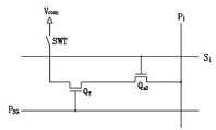
접촉 감지부는 도 4에 도시한 바와 같이 공통 전압(Vcom)에 연결되어 있는 스위치(SWT), 스위치(SWT)와 신호선(PSG)에 연결된 감지 소자(QT) 및 신호선(S1-SN, P1-PM) 중 일부에 연결된 스위칭 소자(QS2)를 포함하며, 신호선(S1-SN, P1-PM)이 교차하는 부분 중 광감지부가 없는 부분에 형성되어 있다.As illustrated in FIG. 4, the touch sensing unit includes a switch SWT connected to the common voltage Vcom , a sensing element QT connected to the switch SWT, and a signal line PSG , and a signal line S1 -S.N, includes a switching element (QS2) are connected to some of the P1 -PM), signal lines(S 1 -S N, P 1 -P M) is formed on the portion without light sensing portion of an intersection .
스위치(SWT)는 사용자의 접촉에 따라 공통 전압(Vcom)을 감지 소자(QT)에 전달한다.The switch SWT transfers the common voltage Vcom to the sensing element QT according to the contact of the user.
감지 소자(QT)는 삼단자 소자로서 그 제어 단자 및 입력 단자는 각각 제어 전압선(PSG)과 스위치(SWT)에 연결되어 있으며, 출력 단자는 스위칭 소자(QS2)에 연결되어 있다. 감지 소자(QT)는 스위치(SWT)로부터 전달된 공통 전압(Vcom)에 따른 감지 전류를 출력한다.The sensing element QT is a three-terminal element whose control terminal and input terminal are connected to the control voltage line PSG and the switch SWT, respectively, and the output terminal is connected to the switching element QS2 . The sensing element QT outputs a sensing current according to the common voltage Vcom transmitted from the switch SWT.
스위칭 소자(QS2) 역시 삼단자 소자로서 그 제어 단자, 출력 단자 및 입력 단자는 각각 감지 주사선(S1-SN), 감지 신호선(P1-PM) 및 감지 소자(QT)에 연결되어 있다. 스위칭 소자(QS2)는 감지 주사선(S1-SN)에 스위칭 소자(QS2)를 턴 온시키는 전압이 인가되면 감지 소자(QT)로부터의 감지 전류를 접촉 감지 신호(VP1-VPM)로서 감지 신호선(P1-PM)으로 출력한다.The switching element QS2 is also a three-terminal element whose control terminal, output terminal and input terminal are connected to the sensing scan lines S1 -SN , the sensing signal lines P1 -PM and the sensing elements QT, respectively. It is. A switching element (QS2) detects the scanning line (S1 -SN) to the switching elements when a voltage for turning on the (QS2) applied to the sensing element detects a touch sensing current from the (QT) signal (VP1 -VPM ) to the sensing signal lines P1 -PM.
여기서 스위칭 소자(Q, QS1, QS2) 및 감지 소자(QP, QT)는 비정질 규소 (amorphous silicon) 또는 다결정 규소(poly crystalline silicon) 박막 트랜지스터로 이루어질 수 있다.The switching elements Q, QS1 and QS2 and the sensing elements QP and QT may be formed of amorphous silicon or poly crystalline silicon thin film transistors.
그러면 이러한 접촉 감지부의 구조 및 동작에 대하여 도 5a 및 도 5b를 참고로 하여 상세하게 설명한다.Next, the structure and operation of the touch sensing unit will be described in detail with reference to FIGS. 5A and 5B.
도 5a 및 도 5b는 본 발명의 한 실시예에 따른 액정 표시 장치의 접촉 감지부의 구조 및 동작을 설명하기 위한 개략도이다.5A and 5B are schematic diagrams for describing a structure and an operation of the touch sensing unit of the liquid crystal display according to the exemplary embodiment.
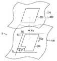
도 5a에는 아무런 접촉이 없는 상태의 본 발명의 한 실시예에 따른 액정 표시 장치의 단면이 도시되어 있다. 도 5a에 보이는 것처럼, 하부 표시판(100)에는 절연 기판(110) 위에 화소층(115)이 형성되어 있다. 화소층(115)에는 화소 및 감지부 등이 형성되어 있으며, 화소층(115) 위에 접촉 감지부의 감지 소자(QT)의 입력 단자 전극(196)이 드러나 있다.FIG. 5A is a cross-sectional view of a liquid crystal display according to an exemplary embodiment of the present invention without any contact. As illustrated in FIG. 5A, a
하부 표시판(100)과 마주하는 상부 표시판(200)에는 투명한 유리 등의 절연 물질로 이루어진 기판(210) 위에 블랙 매트릭스라고 하는 차광 부재(220)가 형성되어 있다. 차광 부재(220)는 화소 사이의 빛샘을 방지한다.On the
복수의 색필터(230)가 기판(210)과 차광 부재(220) 위에 형성되어 있으며, 차광 부재(220)가 정의하는 개구 영역 내에 거의 들어가도록 배치되어 있다.The plurality of
색필터(230) 및 차광 부재(220) 위에는 유기 물질 따위로 이루어진 덮개막(overcoat)(250)이 형성되어 색필터(230)를 보호하고 표면을 평탄하게 한다.An
덮개막(250) 위에는 유기 물질 따위로 이루어진 복수의 돌출부(240)가 형성 되어 있다. 돌출부(240)는 감지 소자(QT)의 입력 단자 전극(196)이 형성되어 있는 위치에 대응하여 배치된다. 돌출부(240)는 유기막 등을 도포하고 패터닝함으로써 원하는 형상 및 높이로 형성할 수 있다.A plurality of
덮개막(250) 및 돌출부(240) 위에는 ITO(indium tin oxide) 또는 IZO(indium zinc oxide) 등의 투명한 도전 물질로 이루어져 있는 공통 전극(270)이 형성되어 있다. 공통 전극(270)에는 공통 전압(Vcom)이 인가된다.A
또는 덮개막(250) 위에 1차 ITO 또는 IZO를 선증착한 후 그 위에 유기막을 코팅하고 패터닝함으로써 돌출부(240)를 형성하고, 다시 돌출부(240) 및 덮개막(250) 위에 10~300㎚의 2차 ITO 또는 IZO를 증착할 수도 있다.Alternatively, after the first ITO or IZO is deposited on the
하부 표시판(100)과 상부 표시판(200)의 사이에는 액정층(3)이 들어 있으며, 두 표시판(100, 200)은 복수의 비즈 스페이서(320)에 의하여 지지되어 있어서 돌출부(240)를 둘러싼 공통 전극(270)과 입력 단자 전극(196)은 일정한 간격을 유지하고 있으며, 그 간격은 0.1㎛~1.0㎛가 되도록 한다.The liquid crystal layer 3 is disposed between the
두 표시판(100, 200)은 컬럼 스페이서(245, 도 7 참조)에 의하여 지지될 수도 있다.The two
돌출부(240)를 둘러싼 공통 전극(270)과 입력 단자 전극(196)은 접촉 감지부의 스위치(SWT)를 이룬다.The
도 5b에는 사용자의 손가락 등이 접촉을 한 상태의 본 발명의 한 실시예에 따른 액정 표시 장치의 단면이 도시되어 있다. 도 5b에 보이는 것처럼, 상부 표시 판(200)은 접촉에 따른 압력에 의하여 눌려져 그 접촉점 부위의 돌출부(240)를 둘러싼 공통 전극(270)이 하부 표시판(100)의 입력 단자 전극(196)에 전기적?물리적으로 연결된다. 이에 따라 공통 전압(Vcom)이 입력 단자 전극(196)에 전달되어 감지 소자(QT)가 감지 전류를 흘린다.5B is a cross-sectional view of the liquid crystal display according to the exemplary embodiment of the present invention in a state where a user's finger or the like is in contact. As shown in FIG. 5B, the
광감지부는 사용자가 접촉한 부분에만 그림자가 드리워져 접촉된 위치를 감지할 수 있으나, 접촉 감지부는 사용자의 접촉(압력)에 의하여 유리 등으로 이루어진 액정 표시판 조립체(300) 전체가 눌리므로 넓은 면적에 걸쳐 복수의 스위치(SWT)가 접촉하게 되어 접촉된 위치를 감지하기 어렵고 단지 접촉 여부만을 감지할 수 있다.The light sensing unit may detect a position where a shadow is cast only on a portion where the user touches, but the touch sensing unit is pressed by a user's contact (pressure) so that the entire liquid
다시 도 1을 참고하면, 계조 전압 생성부(550)는 화소의 투과율과 관련된 두 벌의 복수 계조 전압을 생성한다. 두 벌 중 한 벌은 공통 전압(Vcom)에 대하여 양의 값을 가지고 다른 한 벌은 음의 값을 가진다.Referring back to FIG. 1, the gray voltage generator 550 generates two sets of gray voltages related to the transmittance of the pixel. One of the two sets has a positive value for the common voltage (Vcom ) and the other set has a negative value.
영상 주사부(400)는 액정 표시판 조립체(300)의 영상 주사선(G1-Gn)에 연결되어 게이트 온 전압(Von)과 게이트 오프 전압(Voff)의 조합으로 이루어진 영상 주사 신호를 영상 주사선(G1-Gn)에 인가한다.The
데이터 구동부(500)는 액정 표시판 조립체(300)의 데이터선(D1-Dm)에 연결되어 계조 전압 생성부(550)로부터의 계조 전압을 선택하여 데이터 신호로서 화소에 인가한다.The
감지 주사부(700)는 액정 표시판 조립체(300)의 감지 주사선(S1-SN)에 연결되어 게이트 온 전압(Von)과 게이트 오프 전압(Voff)의 조합으로 이루어진 감지 주사 신호를 감지 주사선(S1-SN)에 인가한다.The
신호 판독부(800)는 액정 표시판 조립체(300)의 감지 신호선(P1-PM)에 연결되어 감지 신호선(P1-PM)을 통하여 출력되는 감지 신호(VP1-VPM)를 입력받아 증폭, 필터링 등의 신호 처리를 행한 후 아날로그-디지털 변환을 하여 디지털 감지 신호(DSN)를 내보낸다.
신호 제어부(600)는 영상 주사부(400), 데이터 구동부(500), 감지 주사부(700), 그리고 신호 판독부(800) 등의 동작을 제어한다.The
영상 주사부(400), 데이터 구동부(500), 감지 주사부(700) 또는 신호 판독부(800)는 복수의 구동 집적 회로 칩의 형태로 액정 표시판 조립체(300) 위에 직접 장착되거나, 가요성 인쇄 회로막(flexible printed circuit film)(도시하지 않음) 위에 장착되어 TCP(tape carrier package)의 형태로 액정 표시판 조립체(300)에 부착될 수도 있다. 이와는 달리, 영상 주사부(400), 데이터 구동부(500), 감지 주사부(700) 또는 신호 판독부(800)가 액정 표시판 조립체(300)에 집적될 수도 있다. 또는 데이터 구동부(500), 신호 판독부(800) 및 신호 제어부(600) 등은 원 칩(one-chip)이라고도 하는 하나의 IC 안에 집적되어 구현될 수도 있다.The
그러면 이러한 액정 표시 장치의 표시 동작 및 감지 동작에 대하여 좀더 상 세하게 설명한다.Next, the display operation and the detection operation of the liquid crystal display will be described in more detail.
신호 제어부(600)는 외부의 그래픽 제어기(도시하지 않음)로부터 입력 영상 신호(R, G, B) 및 이의 표시를 제어하는 입력 제어 신호, 예를 들면 수직 동기 신호(Vsync)와 수평 동기 신호(Hsync), 메인 클록(MCLK), 데이터 인에이블 신호(DE) 등을 제공받는다. 신호 제어부(600)는 입력 영상 신호(R, G, B)와 입력 제어 신호를 기초로 영상 신호(R, G, B)를 액정 표시판 조립체(300)의 동작 조건에 맞게 적절히 처리하고 영상 주사 제어 신호(CONT1) 및 데이터 제어 신호(CONT2) 등을 생성한 후, 영상 주사 제어 신호(CONT1)를 영상 주사부(400)로 내보내고 데이터 제어 신호(CONT2)와 처리한 영상 신호(DAT)는 데이터 구동부(500)로 내보낸다. 또한 신호 제어부(600)는 입력 제어 신호를 기초로 감지 주사 제어 신호(CONT3) 및 판독 제어 신호(CONT4)를 생성한 후, 감지 주사 제어 신호(CONT3)를 감지 주사부(700)에 내보내고 판독 제어 신호(CONT4)를 신호 판독부(800)에 내보낸다.The
영상 주사 제어 신호(CONT1)는 게이트 온 전압(Von)의 주사 시작을 지시하는 주사 시작 신호(STV)와 게이트 온 전압(Von)의 출력을 제어하는 적어도 하나의 클록 신호 등을 포함한다.Image scan control signal (CONT1) includes at least one clock signal and the like to control the output of the start scan indicating the scanning start of a gate-on voltage (Von) signal (STV) and the gate-on voltage (Von).
데이터 제어 신호(CONT2)는 한 화소행의 데이터 전송을 알리는 수평 동기 시작 신호(STH)와 데이터선(D1-Dm)에 해당 데이터 전압을 인가하라는 로드 신호(LOAD), 공통 전압(Vcom)에 대한 데이터 전압의 극성(이하 "공통 전압에 대한 데이 터 전압의 극성"을 줄여 "데이터 전압의 극성"이라 함)을 반전시키는 반전 신호(RVS) 및 데이터 클록 신호(HCLK) 등을 포함한다.The data control signal CONT2 is a horizontal synchronization start signal STH for transmitting data of one pixel row, a load signal LOAD for applying a corresponding data voltage to the data lines D1 -Dm , and a common voltage Vcom. And the inversion signal RVS and the data clock signal HCLK for inverting the polarity of the data voltage (hereinafter referred to as "polarity of the data voltage" by reducing the "polarity of the data voltage" for the common voltage)). .
데이터 구동부(500)는 신호 제어부(600)로부터의 데이터 제어 신호(CONT2)에 따라 한 행의 화소에 대한 영상 데이터(DAT)를 입력받고, 계조 전압 생성부(550)로부터의 계조 전압 중 각 영상 데이터(DAT)에 대응하는 계조 전압을 선택함으로써, 영상 데이터(DAT)를 해당 데이터 전압으로 변환한 후 이를 해당 데이터선(D1-Dm)에 인가한다.The
영상 주사부(400)는 신호 제어부(600)로부터의 영상 주사 제어 신호(CONT1)에 따라 게이트 온 전압(Von)을 영상 주사선(G1-Gn)에 인가하여 이 영상 주사선(G1-Gn)에 연결된 스위칭 소자(Q)를 턴 온시키며, 이에 따라 데이터선(D1-Dm)에 인가된 데이터 전압이 턴 온된 스위칭 소자(Q)를 통하여 해당 화소에 인가된다.The
화소에 인가된 데이터 전압과 공통 전압(Vcom)의 차이는 액정 축전기(CLC)의 충전 전압, 즉 화소 전압으로서 나타난다. 액정 분자들은 화소 전압의 크기에 따라 그 배열을 달리하며, 이에 따라 액정층(3)을 통과하는 빛의 편광이 변화한다. 이러한 편광의 변화는 표시판(100, 200)에 부착된 편광자(도시하지 않음)에 의하여 빛의 투과율 변화로 나타난다.The difference between the data voltage applied to the pixel and the common voltage Vcom is shown as the charging voltage of the liquid crystal capacitor CLC , that is, the pixel voltage. The arrangement of the liquid crystal molecules varies according to the magnitude of the pixel voltage, thereby changing the polarization of light passing through the liquid crystal layer 3. The change in polarization is represented by a change in transmittance of light by a polarizer (not shown) attached to the
1 수평 주기(또는 "1H")[수평 동기 신호(Hsync), 데이터 인에이블 신호(DE)의 한 주기]가 지나면 데이터 구동부(500)와 영상 주사부(400)는 다음 행의 화소에 대 하여 동일한 동작을 반복한다. 이러한 방식으로, 한 프레임(frame) 동안 모든 영상 주사선(G1-Gn)에 대하여 차례로 게이트 온 전압(Von)을 인가하여 모든 화소에 데이터 전압을 인가한다. 한 프레임이 끝나면 다음 프레임이 시작되고 각 화소에 인가되는 데이터 전압의 극성이 이전 프레임에서의 극성과 반대가 되도록 데이터 구동부(500)에 인가되는 반전 신호(RVS)의 상태가 제어된다("프레임 반전"). 이때, 한 프레임 내에서도 반전 신호(RVS)의 특성에 따라 한 데이터선을 통하여 흐르는 데이터 전압의 극성이 바뀌거나(보기: 행반전, 점반전), 한 화소행에 인가되는 데이터 전압의 극성도 서로 다를 수 있다(보기: 열반전, 점반전).After one horizontal period (or "1H") (one period of the horizontal sync signal Hsync and the data enable signal DE) has passed, the
감지 주사부(700)는 신호 제어부(600)로부터의 감지 주사 제어 신호(CONT3)에 따라 게이트 온 전압(Von)을 감지 주사선(S1-SN)에 인가하여 이 감지 주사선(S1-SN)에 연결된 스위칭 소자(QS1, QS2)를 턴 온시키며, 이에 따라 광감지부 및/또는 접촉 감지부로부터의 감지 신호(VP1-VPM)가 턴 온된 스위칭 소자(QS1, QS2)를 통하여 해당 감지 신호선(P1-PM)에 인가된다.Detecting the
신호 판독부(800)는 판독 제어 신호(CONT4)에 따라 감지 신호선(P1-PM)에 인가되어 있는 감지 신호(VP1-VPM)를 읽어 들인다. 신호 판독부(800)는 읽어 들인 감지 신호(VP1-VPM)를 증폭 및 필터링 등의 신호 처리를 한 후 디지털 신호(DSN)로 변환하여 외부 장치로 내보낸다. 외부 장치는 이 디지털 신호(DSN)에 대하여 적절한 연산 처리를 행하여 접촉 여부 및 접촉 위치를 알아내고 이에 기초한 영상 신호를 액정 표시 장치에 전송한다.The
감지 동작은 앞서 설명한 표시 동작과 별도로 수행되며, 서로 영향을 받지 않는다. 한 화소행에 대한 감지 동작은 광감지부 및 접촉 감지부의 형성 밀도에 따라 1 수평 주기 또는 복수의 수평 주기마다 이루어진다. 또한 한 화소에 대한 감지 동작은 매 프레임마다 반드시 이루어질 필요는 없으며 필요에 따라 복수의 프레임마다 한번씩 이루어질 수도 있다.The sensing operation is performed separately from the display operation described above, and is not affected by each other. The sensing operation for one pixel row is performed every one horizontal period or a plurality of horizontal periods according to the formation density of the light sensing unit and the touch sensing unit. In addition, the sensing operation of one pixel does not necessarily need to be performed every frame, and may be performed once for each of a plurality of frames as necessary.
그러면 본 발명의 실시예에 따른 액정 표시 장치의 화소 및 감지부의 배열에 대하여 도면을 참고로 하여 상세하게 설명한다.Next, an arrangement of the pixel and the sensing unit of the liquid crystal display according to the exemplary embodiment of the present invention will be described in detail with reference to the accompanying drawings.
도 6은 본 발명의 실시예에 따른 액정 표시 장치의 화소 및 감지부 배열의 한 예를 도시한 개략도이고, 도 7은 본 발명의 실시예에 따른 액정 표시 장치의 화소 및 감지부 배열의 다른 예를 도시한 개략도이며, 도 8은 본 발명의 실시예에 따른 액정 표시 장치의 공통 전압과 주사 신호의 타이밍도의 한 예이다.6 is a schematic diagram illustrating an example of an arrangement of a pixel and a sensing unit of a liquid crystal display according to an exemplary embodiment of the present invention, and FIG. 7 is another example of an arrangement of a pixel and a sensing unit of a liquid crystal display according to an exemplary embodiment of the present invention. 8 is an example of a timing diagram of a common voltage and a scan signal of a liquid crystal display according to an exemplary embodiment of the present invention.
우선 도 6을 참고로 하여 감지부가 화소 내부에 포함되어 있는 경우에 대하여 설명한다.First, a case in which the sensing unit is included in the pixel will be described with reference to FIG. 6.
도 6에 보이는 것처럼, 하나의 행(R)과 하나의 열(C)이 교차되는 영역(편의상 사각형으로 도시한다)에 하나의 화소가 배치된다. 설명의 편의를 위하여 i번째 행과 j번째 열이 교차하는 영역을 (Ri, Cj)라 표시한다.As shown in FIG. 6, one pixel is disposed in an area (shown as a rectangle for convenience) where one row R and one column C intersect. For convenience of explanation, the region where the i-th row and the j-th column intersect is indicated as (Ri, Cj).
하나의 도트는 R, G, B 화소 3개로 이루어지며 하나의 색상을 표시하는 단위가 된다. 도 6에서는 한 행과 세 열이 교차하는 3개의 영역에 각각 배치되어 있는 세 개의 화소가 하나의 도트를 이룬다.One dot is composed of three R, G, and B pixels, and becomes a unit for displaying one color. In FIG. 6, three pixels arranged in three regions where one row and three columns intersect form one dot.
광감지부는 액정 표시 장치 해상도의 1/4의 해상도를 가진다. 예를 들어, 액정 표시 장치가 240*320의 QVGA(quarter video graphics array)의 해상도를 가진다고 하면 광감지부는 120*160의 QQVGA(quarter QVGA)의 해상도를 가진다. 그러면 문자 인식과 같이 정밀도가 높은 응용 분야에서 이러한 광감지부를 내장한 액정 표시 장치를 이용할 수 있다. 물론 광감지부의 해상도는 필요에 따라 더 높거나 낮은 해상도를 가질 수도 있다.The light sensing unit has a resolution of 1/4 of the resolution of the liquid crystal display. For example, if the liquid crystal display has a resolution of a quarter video graphics array (QVGA) of 240 * 320, the light sensing unit has a resolution of QQVGA (quarter QVGA) of 120 * 160. Then, the liquid crystal display having the optical sensing unit may be used in high precision applications such as character recognition. Of course, the resolution of the light sensing unit may have a higher or lower resolution as necessary.
접촉 감지부는 광감지부의 해상도 이하의 해상도를 가지며 광감지부가 배치되어 있지 않은 화소에 배치된다. 광감지부와 접촉 감지부가 동일한 해상도를 가지는 경우라면 이들은 도트 열에 대하여 교대로 배치된다. 예를 들어 광감지부가 홀수 번째 도트 열에 배치되면 접촉 감지부는 짝수 번째 도트 열에 배치된다. 이때 광감지부 및 접촉 감지부는 홀수 번째 행 및 짝수 번째 행 중 임의의 한 행에 배치될 수 있다. 즉, 일례로 광감지부는 (R1, C2), (R1, C8), (R1, C14), ..., (R3, C2), (R3, C8), (R3, C14), ..., (R5, C2), (R5, C8), (R5, C14), ...에 배치될 수 있고, 접촉 감지부는 (R1, C5), (R1, C11), ..., (R3, C5), (R3, C11), ..., (R5, C5), (R5, C11), ...에 배치될 수 있다.The touch sensing unit is disposed in a pixel having a resolution equal to or less than that of the light sensing unit and in which the light sensing unit is not disposed. If the light sensing unit and the contact sensing unit have the same resolution, they are alternately arranged with respect to the dot row. For example, when the light sensing unit is disposed in the odd dot rows, the touch sensing unit is disposed in the even dot rows. In this case, the light sensing unit and the touch sensing unit may be disposed in any one of odd and even rows. That is, as an example, the light sensing unit includes (R1, C2), (R1, C8), (R1, C14), ..., (R3, C2), (R3, C8), (R3, C14), ... , (R5, C2), (R5, C8), (R5, C14), ..., the contact sensing unit (R1, C5), (R1, C11), ..., (R3, C5), (R3, C11), ..., (R5, C5), (R5, C11), ... can be disposed.
한편 한 도트 내의 3개 또는 2개의 화소에 광감지부를 각각 배치하고 이들 광감지부의 감지 신호선을 서로 연결하여 각 광감지부의 감지 신호를 중첩시킬 수도 있다. 이와 같이 중첩되어 더해진 감지 신호에 의하면 각 광감지부의 특성 편차를 줄일 수 있으며, 데이터선(D1-Dm)에 인가되어 있는 데이터 전압의 영향을 줄일 수 있다. 여기서 광감지부의 해상도는 개개의 광감지부의 해상도를 의미하는 것이 아니라 하나의 감지 신호에 의하여 파악되는 해상도를 의미한다.On the other hand, the light sensing unit may be disposed on three or two pixels in one dot, and the sensing signal lines of the light sensing unit may be connected to each other to overlap the sensing signals of the respective light sensing units. According to the overlapped sensing signals, the characteristic variation of each light sensing unit can be reduced, and the influence of the data voltage applied to the data lines D1 -Dm can be reduced. Here, the resolution of the photodetector does not mean the resolution of the individual photodetectors but means a resolution which is detected by one sensing signal.
또는 세로로 배열된 2개의 도트 중 상하로 배치되어 있는 두 화소에 광감지부를 각각 배치하고 이들 광감지부의 감지 주사선을 서로 연결함으로써 이들 광감지부의 감지 신호를 동일한 감지 신호선에 중첩시켜 내보낼 수 있다. 이렇게 중첩되어 더해진 감지 신호에 의하면 각 광감지부의 특성 편차를 줄일 수 있을 뿐만 아니라 신호 대 잡음비(signal to noise ratio)도 2배가 되어 보다 정확한 감지 신호를 추출할 수 있다. 이 경우 공통 전압(Vcom)과 주사 신호의 타이밍에 대하여 도 8을 참고로 하여 상세하게 설명한다.Alternatively, the light sensing units may be superimposed on two pixels arranged vertically, and the sensing scan lines of the light sensing units may be connected to each other, and the sensing signals may be superimposed on the same sensing signal lines. The superimposed sensing signals not only reduce the characteristic variation of each optical sensing unit, but also double the signal to noise ratio to extract more accurate sensing signals. In this case, the timing of the common voltage Vcom and the scan signal will be described in detail with reference to FIG. 8.
도 8에 도시한 바와 같이, 공통 전압(Vcom)은 1H 단위로 하이 레벨과 로우 레벨을 스윙하는 신호이고, 프레임마다 그 레벨이 반전된다.As shown in FIG. 8, the common voltage Vcom is a signal swinging the high level and the low level in units of 1H, and the level is inverted for each frame.
영상 주사 신호(g1-gn)는 1H 마다 차례로 게이트 온 전압(Von)이 되어 영상 주사선(G1-Gn)에 인가된다.The image scanning signals g1- gn are applied to the image scanning lines G1 -Gn at the same time as the gate-on voltages Von every 1H.
감지 주사 신호(sg1-sgN)는 홀수 번째 프레임에서는 홀수 번째 영상 주사 신호(g2k-1)에 동기되어 게이트 온 전압(Von)이 되고, 짝수 번째 프레임에서는 짝수 번째 영상 주사 신호(g2k)에 동기되어 게이트 온 전압(Von)이 된다. 이와 같이 하면, 모든 감지 소자가 공통 전압(Vcom)이 항상 하이 레벨인 때에 감지 동작을 하게 되므 로, 즉, 공통 전압(Vcom)에 의한 커플링(coupling) 효과가 균일한 상태에서 감지 동작을 하므로 감지 신호의 왜곡을 최소화할 수 있다. 이와 반대로 모든 감지 소자가 공통 전압(Vcom)이 항상 로우 레벨인 때에 감지 동작을 할 수도 있으며, 그 효과는 동일하다.The sensing scan signals sg1 -sgN become the gate-on voltage Von in synchronization with the odd-numbered image scan signal g2k-1 in odd- numbered frames, and the even-numbered image scan signal g in even-numbered frames.2k ) to become the gate-on voltage (Von ). In this way, all the sensing elements perform a sensing operation when the common voltage Vcom is always at a high level, that is, a sensing operation in a state where the coupling effect by the common voltage Vcom is uniform. Therefore, the distortion of the detection signal can be minimized. In contrast, all sensing elements may perform sensing operations when the common voltage Vcom is always at a low level, and the effect is the same.
다음으로 도 7을 참고로 하여 감지부가 화소 영역 밖의 별도의 영역에 배치되는 경우의 화소 및 감지부의 배열에 대하여 설명한다.Next, the arrangement of the pixel and the sensing unit in the case where the sensing unit is disposed in a separate area outside the pixel area will be described with reference to FIG. 7.
도 7에 도시한 바와 같이 화소는 P로 표시한 열에 배치되고, 감지부는 S로 표시한 열에 배치된다. 설명의 편의를 위하여 i번째 행과 j번째 화소 열이 교차하는 영역을 (Ri, Pj)라 표시하고, i번째 행과 j번째 감지부 열이 교차하는 영역을 (Ri, Sj)라 표시한다.As shown in FIG. 7, the pixels are arranged in columns denoted by P, and the sensing unit is arranged in columns denoted by S. FIG. For convenience of explanation, the region where the i-th row and the j-th pixel column intersect is denoted by (Ri, Pj), and the region where the i-th row and the j-th detector column intersect is denoted by (Ri, Sj).
하나의 도트는 한 행과 세 개의 화소 열(P)이 교차하는 3개의 영역 및 동일한 행과 이들 화소 열(P)과 인접해 있는 감지부 열(S)이 교차하는 하나의 영역을 포함한다.One dot includes three regions in which one row and three pixel columns P intersect, and one region in which the same row intersects the sensing unit column S adjacent to these pixel columns P. FIG.
도 6에 도시한 감지부와 마찬가지로 광감지부는 액정 표시 장치 해상도의 1/4의 해상도를 가지며, 접촉 감지부는 광감지부의 해상도 이하의 해상도를 가진다. 두 개의 인접한 감지부 열(S) 중 어느 하나에 광감지부가 배치되고 다른 하나에 접촉 감지부가 배치된다. 한 예로서 홀수 번째 감지부 열(S)에 광감지부가 배치되고, 짝수 번째 감지부 열(S)에 접촉 감지부가 배치될 수 있다. 이때 광감지부 및 접촉 감지부는 홀수 번째 행 및 짝수 번째 행 중 임의의 한 행에 배치될 수 있 다.Like the sensing unit shown in FIG. 6, the light sensing unit has a resolution of 1/4 of the resolution of the liquid crystal display, and the touch sensing unit has a resolution equal to or less than that of the light sensing unit. The light sensing unit is disposed in any one of two adjacent sensing unit rows S, and the touch sensing unit is disposed in the other. As an example, the light detector may be disposed in the odd-numbered detector column S, and the touch detector may be disposed in the even-numbered detector column S. FIG. In this case, the light sensing unit and the touch sensing unit may be disposed in any one of odd rows and even rows.
예를 들어, 광감지부는 (R1, S1), (R1, S3), ..., (R3, S1), (R3, S3), ..., (R5, S1), (R5, S3), ...에 배치되며, 접촉 감지부는 (R1, S2), (R1, S4), ..., (R5, S2), (R5, S4), ...에 배치될 수 있다. 이때 접촉 감지부의 해상도는 광감지부의 해상도의 반이다.For example, the light sensing unit (R1, S1), (R1, S3), ..., (R3, S1), (R3, S3), ..., (R5, S1), (R5, S3) , ... may be disposed, and the touch sensing unit may be disposed at (R1, S2), (R1, S4), ..., (R5, S2), (R5, S4),. In this case, the resolution of the touch sensing unit is half the resolution of the light sensing unit.
한편, 도 7에 보이는 것처럼, 접촉 감지부가 형성되어 있는 감지부 열에 해당하는 영역(S2, S4, ...)에 돌출부(240) 및 컬럼 스페이서(245)가 놓인다. 컬럼 스페이서(245)는 감지부 열(S)에서 접촉 감지부가 형성되지 않은 곳에 배치한다. 도 7에는 컬럼 스페이서(245) 3개를 도시하였으나 필요에 따라 그 수효는 가감된다. 또한 별도로 도시되어 있지 않지만 광감지부가 배치되어 있는 감지부 열(S)에도 컬럼 스페이서(245)가 놓일 수 있다.On the other hand, as shown in Figure 7, the
앞선 예에서와 마찬가지로 광감지부가 배치되는 감지부 열 전체에 광감지부를 배치하고 두 행씩 감지 주사선을 연결함으로써 이렇게 연결되어 있는 광감지부의 감지 신호를 동일한 감지 신호선에 중첩시켜 내보낼 수 있다. 이 경우 공통 전압(Vcom)과 감지 주사 신호의 관계는 도 8에 도시한 타이밍도를 따른다.As in the previous example, by placing the light sensing unit in the entire sensing column where the light sensing unit is arranged and connecting the sensing scan lines in two rows, the sensing signals of the connected light sensing units can be superimposed on the same sensing signal line. In this case, the relationship between the common voltage Vcom and the sensing scan signal follows the timing chart shown in FIG. 8.
이와 같이 본 발명에 의하면, 소정 배열을 가지는 광감지부와 접촉 감지부를 구비함으로써 접촉 여부 및 접촉 위치를 정확하게 감지할 수 있는 감지 신호를 생성할 수 있다.Thus, according to the present invention, by providing a light sensing unit and a touch sensing unit having a predetermined arrangement it is possible to generate a detection signal that can accurately detect whether the contact and the contact position.
이상에서 본 발명의 바람직한 실시예에 대하여 상세하게 설명하였지만 본 발명의 권리범위는 이에 한정되는 것은 아니고 다음의 청구범위에서 정의하고 있는 본 발명의 기본 개념을 이용한 당업자의 여러 변형 및 개량 형태 또한 본 발명의 권리범위에 속하는 것이다.Although the preferred embodiments of the present invention have been described in detail above, the scope of the present invention is not limited thereto, and various modifications and improvements of those skilled in the art using the basic concepts of the present invention defined in the following claims are also provided. It belongs to the scope of rights.
Claims (14)
Translated fromKoreanPriority Applications (5)
| Application Number | Priority Date | Filing Date | Title |
|---|---|---|---|
| KR1020040090376AKR101160826B1 (en) | 2004-11-08 | 2004-11-08 | Liquid crystal display including sensing element |
| TW094138962ATWI438692B (en) | 2004-11-08 | 2005-11-07 | Display device including sensing elements |
| CNB2005101156840ACN100529849C (en) | 2004-11-08 | 2005-11-08 | Display device including sensing elements |
| US11/270,151US20060097975A1 (en) | 2004-11-08 | 2005-11-08 | Display device including sensing elements |
| JP2005324190AJP4920245B2 (en) | 2004-11-08 | 2005-11-08 | Liquid crystal display with a sensing element |
Applications Claiming Priority (1)
| Application Number | Priority Date | Filing Date | Title |
|---|---|---|---|
| KR1020040090376AKR101160826B1 (en) | 2004-11-08 | 2004-11-08 | Liquid crystal display including sensing element |
Publications (2)
| Publication Number | Publication Date |
|---|---|
| KR20060041023A KR20060041023A (en) | 2006-05-11 |
| KR101160826B1true KR101160826B1 (en) | 2012-06-29 |
Family
ID=36315823
Family Applications (1)
| Application Number | Title | Priority Date | Filing Date |
|---|---|---|---|
| KR1020040090376AExpired - Fee RelatedKR101160826B1 (en) | 2004-11-08 | 2004-11-08 | Liquid crystal display including sensing element |
Country Status (5)
| Country | Link |
|---|---|
| US (1) | US20060097975A1 (en) |
| JP (1) | JP4920245B2 (en) |
| KR (1) | KR101160826B1 (en) |
| CN (1) | CN100529849C (en) |
| TW (1) | TWI438692B (en) |
Families Citing this family (43)
| Publication number | Priority date | Publication date | Assignee | Title |
|---|---|---|---|---|
| US7518613B2 (en)* | 2006-01-11 | 2009-04-14 | Dell Products L.P. | System and method for information handling system external graphics box local diagnostic message |
| JP4834482B2 (en)* | 2006-07-24 | 2011-12-14 | 東芝モバイルディスプレイ株式会社 | Display device |
| JP2008083322A (en)* | 2006-09-27 | 2008-04-10 | Seiko Epson Corp | Display device with input function |
| JP4497328B2 (en)* | 2006-10-25 | 2010-07-07 | セイコーエプソン株式会社 | Electro-optical device and electronic apparatus |
| KR101292765B1 (en)* | 2006-10-31 | 2013-08-02 | 삼성디스플레이 주식회사 | Display Apparatus and Method of Fabricating the Same |
| US9710095B2 (en)* | 2007-01-05 | 2017-07-18 | Apple Inc. | Touch screen stack-ups |
| KR101420143B1 (en)* | 2007-02-02 | 2014-07-17 | 삼성디스플레이 주식회사 | Display panel and display apparatus having the same |
| KR101337262B1 (en)* | 2007-02-12 | 2013-12-05 | 삼성디스플레이 주식회사 | Display device and driving method thereof |
| KR101382557B1 (en)* | 2007-06-28 | 2014-04-08 | 삼성디스플레이 주식회사 | Display apparatus |
| TWI360072B (en)* | 2007-07-26 | 2012-03-11 | Au Optronics Corp | Touching panel |
| JP2009031666A (en) | 2007-07-30 | 2009-02-12 | Lg Display Co Ltd | Touch panel integrated display device |
| TWI352922B (en)* | 2007-08-22 | 2011-11-21 | Hannstar Display Corp | Display device and related positioning method |
| KR101437866B1 (en) | 2007-10-15 | 2014-09-05 | 삼성디스플레이 주식회사 | Display device and control method thereof |
| EP2056187A3 (en)* | 2007-10-30 | 2011-05-11 | HannStar Display Corp. | Display device and related positioning method |
| US20090109359A1 (en)* | 2007-10-30 | 2009-04-30 | Po-Sheng Shih | Display device and related positioning method |
| US20090109186A1 (en)* | 2007-10-30 | 2009-04-30 | Hannstar Display Corp. | Display device |
| CN100495129C (en)* | 2007-11-02 | 2009-06-03 | 友达光电股份有限公司 | Optical signal detection method of touch display and display device |
| KR101286543B1 (en) | 2008-05-21 | 2013-07-17 | 엘지디스플레이 주식회사 | Liquid crystal display device |
| JP5191321B2 (en)* | 2008-09-02 | 2013-05-08 | 株式会社ジャパンディスプレイウェスト | Information input device, information input method, information input / output device, and information input program |
| KR100973296B1 (en) | 2008-12-12 | 2010-07-30 | 하이디스 테크놀로지 주식회사 | Built-in touch screen liquid crystal display |
| JP4816738B2 (en)* | 2009-02-05 | 2011-11-16 | ソニー株式会社 | Information input / output device |
| US8654267B2 (en) | 2009-05-27 | 2014-02-18 | Sharp Kabushiki Kaisha | Display device |
| TWI396011B (en)* | 2009-06-16 | 2013-05-11 | Au Optronics Corp | Touch panel |
| US8658957B2 (en) | 2009-06-30 | 2014-02-25 | Sharp Kabushiki Kaisha | Sensor circuit and display apparatus |
| JP2012177953A (en)* | 2009-06-30 | 2012-09-13 | Sharp Corp | Optical sensor and display device |
| EP2472363B1 (en) | 2009-08-27 | 2018-12-19 | Sharp Kabushiki Kaisha | Display device |
| KR101761861B1 (en)* | 2010-06-18 | 2017-07-27 | 삼성디스플레이 주식회사 | Touch sensible display device |
| CN101887184B (en)* | 2010-07-02 | 2011-11-16 | 友达光电股份有限公司 | Pixel array and display panel with the pixel array |
| KR101860934B1 (en)* | 2011-07-08 | 2018-05-25 | 삼성디스플레이 주식회사 | Display device and driving method thereof |
| FR2987929B1 (en) | 2012-03-09 | 2014-04-11 | Digital Art Internat | DEVICE FOR SURFACE DIFFUSION OF LUMINOUS IMAGES AT THE SCALE OF THE HUMAN BODY |
| TWI461896B (en)* | 2012-11-07 | 2014-11-21 | Chih Chung Lin | Photoelectric conversion touch panel |
| CN103838020B (en)* | 2012-11-22 | 2017-09-29 | 群康科技(深圳)有限公司 | Touch control display apparatus and its driving method |
| JP2015055925A (en)* | 2013-09-10 | 2015-03-23 | ソニー株式会社 | Sensor device, method of manufacturing sensor device, display apparatus, and input apparatus |
| JP6434717B2 (en)* | 2014-05-13 | 2018-12-05 | 株式会社ジャパンディスプレイ | Display device |
| FR3028966B1 (en)* | 2014-11-26 | 2018-01-26 | Sequeris | DEVICE AND METHOD FOR CONTROLLING AND APPARATUS COMPRISING SUCH A DEVICE |
| KR102319464B1 (en)* | 2015-03-16 | 2021-10-29 | 삼성디스플레이 주식회사 | Touch device and display including the same |
| CN105116584B (en)* | 2015-09-16 | 2017-02-22 | 深圳市华星光电技术有限公司 | Liquid crystal display panel and device |
| US20170082882A1 (en)* | 2015-09-18 | 2017-03-23 | Semiconductor Energy Laboratory Co., Ltd. | Input/output device and data processor |
| CN105335004B (en)* | 2015-10-28 | 2018-03-23 | 京东方科技集团股份有限公司 | Touch base plate, touch-control display panel and display device |
| CN106648266B (en) | 2015-11-09 | 2023-08-11 | 京东方科技集团股份有限公司 | A display device with pressure-sensitive touch function and driving method |
| CN105242470B (en)* | 2015-11-09 | 2018-09-11 | 武汉华星光电技术有限公司 | A kind of liquid crystal display panel and liquid crystal display device |
| CN107817920B (en)* | 2017-10-31 | 2021-01-12 | 厦门天马微电子有限公司 | Pressure induction sensor driving circuit and driving method, display panel and device |
| CN111179865B (en)* | 2018-11-13 | 2022-07-29 | 咸阳彩虹光电科技有限公司 | Display panel and display method |
Citations (3)
| Publication number | Priority date | Publication date | Assignee | Title |
|---|---|---|---|---|
| JP2001075074A (en)* | 1999-08-18 | 2001-03-23 | Internatl Business Mach Corp <Ibm> | Touch sensor type liquid crystal display device |
| JP2003066417A (en)* | 2001-08-22 | 2003-03-05 | Sharp Corp | Touch sensor integrated display |
| KR20040077269A (en)* | 2003-02-28 | 2004-09-04 | 삼성전자주식회사 | Liquid crystal display and method for manufacturing thereof |
Family Cites Families (11)
| Publication number | Priority date | Publication date | Assignee | Title |
|---|---|---|---|---|
| US6104448A (en)* | 1991-05-02 | 2000-08-15 | Kent State University | Pressure sensitive liquid crystalline light modulating device and material |
| US5543589A (en)* | 1994-05-23 | 1996-08-06 | International Business Machines Corporation | Touchpad with dual sensor that simplifies scanning |
| JPH0980467A (en)* | 1995-09-14 | 1997-03-28 | Toshiba Corp | Active matrix display device with pen input position detection function |
| US6909419B2 (en)* | 1997-10-31 | 2005-06-21 | Kopin Corporation | Portable microdisplay system |
| KR100595922B1 (en)* | 1998-01-26 | 2006-07-05 | 웨인 웨스터만 | Method and apparatus for integrating manual input |
| JP2001175415A (en)* | 1999-12-16 | 2001-06-29 | Ricoh Co Ltd | Coordinate input / detection device |
| JP2003173226A (en)* | 2001-11-27 | 2003-06-20 | Internatl Business Mach Corp <Ibm> | Information processor, program and coordinate input method |
| AU2002336341A1 (en)* | 2002-02-20 | 2003-09-09 | Planar Systems, Inc. | Light sensitive display |
| US7009663B2 (en)* | 2003-12-17 | 2006-03-07 | Planar Systems, Inc. | Integrated optical light sensitive active matrix liquid crystal display |
| US7230608B2 (en)* | 2004-04-23 | 2007-06-12 | Eastman Kodak Company | OLED display and touch screen |
| KR101018751B1 (en)* | 2004-09-24 | 2011-03-04 | 삼성전자주식회사 | Display device and driving method thereof |
- 2004
- 2004-11-08KRKR1020040090376Apatent/KR101160826B1/ennot_activeExpired - Fee Related
- 2005
- 2005-11-07TWTW094138962Apatent/TWI438692B/ennot_activeIP Right Cessation
- 2005-11-08CNCNB2005101156840Apatent/CN100529849C/ennot_activeExpired - Fee Related
- 2005-11-08USUS11/270,151patent/US20060097975A1/ennot_activeAbandoned
- 2005-11-08JPJP2005324190Apatent/JP4920245B2/ennot_activeExpired - Fee Related
Patent Citations (3)
| Publication number | Priority date | Publication date | Assignee | Title |
|---|---|---|---|---|
| JP2001075074A (en)* | 1999-08-18 | 2001-03-23 | Internatl Business Mach Corp <Ibm> | Touch sensor type liquid crystal display device |
| JP2003066417A (en)* | 2001-08-22 | 2003-03-05 | Sharp Corp | Touch sensor integrated display |
| KR20040077269A (en)* | 2003-02-28 | 2004-09-04 | 삼성전자주식회사 | Liquid crystal display and method for manufacturing thereof |
Also Published As
| Publication number | Publication date |
|---|---|
| JP2006133788A (en) | 2006-05-25 |
| JP4920245B2 (en) | 2012-04-18 |
| CN100529849C (en) | 2009-08-19 |
| TW200625174A (en) | 2006-07-16 |
| KR20060041023A (en) | 2006-05-11 |
| TWI438692B (en) | 2014-05-21 |
| US20060097975A1 (en) | 2006-05-11 |
| CN1773335A (en) | 2006-05-17 |
Similar Documents
| Publication | Publication Date | Title |
|---|---|---|
| KR101160826B1 (en) | Liquid crystal display including sensing element | |
| KR101122233B1 (en) | Display device including sensing element | |
| JP5066335B2 (en) | Display device with built-in sensing element | |
| KR101525802B1 (en) | Liquid crystal display | |
| KR100955339B1 (en) | Display panels and display devices capable of detecting touch and access and methods of detecting touch and access using the panel | |
| US8643624B2 (en) | Capacitive sensing using a segmented common voltage electrode of a display | |
| KR101133753B1 (en) | Liquid crystal display including sensing element | |
| KR101152132B1 (en) | Liquid crystal display including sensing unit | |
| KR101230309B1 (en) | Display device and processing apparatus of sensing signal | |
| KR101090254B1 (en) | Display device with integrated sensing element | |
| KR101100884B1 (en) | Display devices and drive devices for display devices | |
| KR101061849B1 (en) | Information recognition device and information recognition display device | |
| CN101620333B (en) | Active matrix display device with touch function | |
| US8581863B2 (en) | Liquid crystal display panel and liquid crystal display apparatus | |
| KR20110137988A (en) | Display with touch sensing | |
| US10185423B2 (en) | Plug-in touch display device and an electronic device | |
| KR101862397B1 (en) | Touch sensor integrated type display | |
| KR20060065333A (en) | Display panels and display devices with sensing elements | |
| KR20060056633A (en) | Display device with integrated sensing element | |
| KR20100120618A (en) | Information detectable display device | |
| TWI376625B (en) | ||
| KR20080044512A (en) | Liquid Crystal Display and Manufacturing Method Thereof | |
| KR20070062692A (en) | Display device and manufacturing method thereof | |
| JP2012247989A (en) | Method of driving image reader | |
| KR20080032790A (en) | Display and liquid crystal display |
Legal Events
| Date | Code | Title | Description |
|---|---|---|---|
| PA0109 | Patent application | St.27 status event code:A-0-1-A10-A12-nap-PA0109 | |
| PN2301 | Change of applicant | St.27 status event code:A-3-3-R10-R13-asn-PN2301 St.27 status event code:A-3-3-R10-R11-asn-PN2301 | |
| PN2301 | Change of applicant | St.27 status event code:A-3-3-R10-R13-asn-PN2301 St.27 status event code:A-3-3-R10-R11-asn-PN2301 | |
| PG1501 | Laying open of application | St.27 status event code:A-1-1-Q10-Q12-nap-PG1501 | |
| R17-X000 | Change to representative recorded | St.27 status event code:A-3-3-R10-R17-oth-X000 | |
| A201 | Request for examination | ||
| PA0201 | Request for examination | St.27 status event code:A-1-2-D10-D11-exm-PA0201 | |
| E902 | Notification of reason for refusal | ||
| PE0902 | Notice of grounds for rejection | St.27 status event code:A-1-2-D10-D21-exm-PE0902 | |
| P11-X000 | Amendment of application requested | St.27 status event code:A-2-2-P10-P11-nap-X000 | |
| P13-X000 | Application amended | St.27 status event code:A-2-2-P10-P13-nap-X000 | |
| PE0902 | Notice of grounds for rejection | St.27 status event code:A-1-2-D10-D21-exm-PE0902 | |
| E13-X000 | Pre-grant limitation requested | St.27 status event code:A-2-3-E10-E13-lim-X000 | |
| P11-X000 | Amendment of application requested | St.27 status event code:A-2-2-P10-P11-nap-X000 | |
| P13-X000 | Application amended | St.27 status event code:A-2-2-P10-P13-nap-X000 | |
| E701 | Decision to grant or registration of patent right | ||
| PE0701 | Decision of registration | St.27 status event code:A-1-2-D10-D22-exm-PE0701 | |
| R18-X000 | Changes to party contact information recorded | St.27 status event code:A-3-3-R10-R18-oth-X000 | |
| GRNT | Written decision to grant | ||
| PR0701 | Registration of establishment | St.27 status event code:A-2-4-F10-F11-exm-PR0701 | |
| PR1002 | Payment of registration fee | St.27 status event code:A-2-2-U10-U11-oth-PR1002 Fee payment year number:1 | |
| PG1601 | Publication of registration | St.27 status event code:A-4-4-Q10-Q13-nap-PG1601 | |
| PN2301 | Change of applicant | St.27 status event code:A-5-5-R10-R11-asn-PN2301 | |
| PN2301 | Change of applicant | St.27 status event code:A-5-5-R10-R11-asn-PN2301 | |
| PN2301 | Change of applicant | St.27 status event code:A-5-5-R10-R14-asn-PN2301 | |
| FPAY | Annual fee payment | Payment date:20150601 Year of fee payment:4 | |
| PR1001 | Payment of annual fee | St.27 status event code:A-4-4-U10-U11-oth-PR1001 Fee payment year number:4 | |
| R18-X000 | Changes to party contact information recorded | St.27 status event code:A-5-5-R10-R18-oth-X000 | |
| LAPS | Lapse due to unpaid annual fee | ||
| PC1903 | Unpaid annual fee | St.27 status event code:A-4-4-U10-U13-oth-PC1903 Not in force date:20160623 Payment event data comment text:Termination Category : DEFAULT_OF_REGISTRATION_FEE | |
| PC1903 | Unpaid annual fee | St.27 status event code:N-4-6-H10-H13-oth-PC1903 Ip right cessation event data comment text:Termination Category : DEFAULT_OF_REGISTRATION_FEE Not in force date:20160623 |