KR101157979B1 - Driving Circuit for Organic Light Emitting Diode and Organic Light Emitting Diode Display Using The Same - Google Patents
Driving Circuit for Organic Light Emitting Diode and Organic Light Emitting Diode Display Using The SameDownload PDFInfo
- Publication number
- KR101157979B1 KR101157979B1KR1020050053120AKR20050053120AKR101157979B1KR 101157979 B1KR101157979 B1KR 101157979B1KR 1020050053120 AKR1020050053120 AKR 1020050053120AKR 20050053120 AKR20050053120 AKR 20050053120AKR 101157979 B1KR101157979 B1KR 101157979B1
- Authority
- KR
- South Korea
- Prior art keywords
- light emitting
- emitting diode
- organic light
- voltage
- transistor
- Prior art date
- Legal status (The legal status is an assumption and is not a legal conclusion. Google has not performed a legal analysis and makes no representation as to the accuracy of the status listed.)
- Expired - Lifetime
Links
Images


Classifications
- G—PHYSICS
- G09—EDUCATION; CRYPTOGRAPHY; DISPLAY; ADVERTISING; SEALS
- G09G—ARRANGEMENTS OR CIRCUITS FOR CONTROL OF INDICATING DEVICES USING STATIC MEANS TO PRESENT VARIABLE INFORMATION
- G09G3/00—Control arrangements or circuits, of interest only in connection with visual indicators other than cathode-ray tubes
- G09G3/20—Control arrangements or circuits, of interest only in connection with visual indicators other than cathode-ray tubes for presentation of an assembly of a number of characters, e.g. a page, by composing the assembly by combination of individual elements arranged in a matrix no fixed position being assigned to or needed to be assigned to the individual characters or partial characters
- G09G3/22—Control arrangements or circuits, of interest only in connection with visual indicators other than cathode-ray tubes for presentation of an assembly of a number of characters, e.g. a page, by composing the assembly by combination of individual elements arranged in a matrix no fixed position being assigned to or needed to be assigned to the individual characters or partial characters using controlled light sources
- G09G3/30—Control arrangements or circuits, of interest only in connection with visual indicators other than cathode-ray tubes for presentation of an assembly of a number of characters, e.g. a page, by composing the assembly by combination of individual elements arranged in a matrix no fixed position being assigned to or needed to be assigned to the individual characters or partial characters using controlled light sources using electroluminescent panels
- G09G3/32—Control arrangements or circuits, of interest only in connection with visual indicators other than cathode-ray tubes for presentation of an assembly of a number of characters, e.g. a page, by composing the assembly by combination of individual elements arranged in a matrix no fixed position being assigned to or needed to be assigned to the individual characters or partial characters using controlled light sources using electroluminescent panels semiconductive, e.g. using light-emitting diodes [LED]
- G09G3/3208—Control arrangements or circuits, of interest only in connection with visual indicators other than cathode-ray tubes for presentation of an assembly of a number of characters, e.g. a page, by composing the assembly by combination of individual elements arranged in a matrix no fixed position being assigned to or needed to be assigned to the individual characters or partial characters using controlled light sources using electroluminescent panels semiconductive, e.g. using light-emitting diodes [LED] organic, e.g. using organic light-emitting diodes [OLED]
- G09G3/3225—Control arrangements or circuits, of interest only in connection with visual indicators other than cathode-ray tubes for presentation of an assembly of a number of characters, e.g. a page, by composing the assembly by combination of individual elements arranged in a matrix no fixed position being assigned to or needed to be assigned to the individual characters or partial characters using controlled light sources using electroluminescent panels semiconductive, e.g. using light-emitting diodes [LED] organic, e.g. using organic light-emitting diodes [OLED] using an active matrix
- G09G3/3233—Control arrangements or circuits, of interest only in connection with visual indicators other than cathode-ray tubes for presentation of an assembly of a number of characters, e.g. a page, by composing the assembly by combination of individual elements arranged in a matrix no fixed position being assigned to or needed to be assigned to the individual characters or partial characters using controlled light sources using electroluminescent panels semiconductive, e.g. using light-emitting diodes [LED] organic, e.g. using organic light-emitting diodes [OLED] using an active matrix with pixel circuitry controlling the current through the light-emitting element
- G—PHYSICS
- G09—EDUCATION; CRYPTOGRAPHY; DISPLAY; ADVERTISING; SEALS
- G09G—ARRANGEMENTS OR CIRCUITS FOR CONTROL OF INDICATING DEVICES USING STATIC MEANS TO PRESENT VARIABLE INFORMATION
- G09G2300/00—Aspects of the constitution of display devices
- G09G2300/04—Structural and physical details of display devices
- G09G2300/0421—Structural details of the set of electrodes
- G09G2300/043—Compensation electrodes or other additional electrodes in matrix displays related to distortions or compensation signals, e.g. for modifying TFT threshold voltage in column driver
- G—PHYSICS
- G09—EDUCATION; CRYPTOGRAPHY; DISPLAY; ADVERTISING; SEALS
- G09G—ARRANGEMENTS OR CIRCUITS FOR CONTROL OF INDICATING DEVICES USING STATIC MEANS TO PRESENT VARIABLE INFORMATION
- G09G2300/00—Aspects of the constitution of display devices
- G09G2300/08—Active matrix structure, i.e. with use of active elements, inclusive of non-linear two terminal elements, in the pixels together with light emitting or modulating elements
- G09G2300/0809—Several active elements per pixel in active matrix panels
- G09G2300/0842—Several active elements per pixel in active matrix panels forming a memory circuit, e.g. a dynamic memory with one capacitor
- G09G2300/0847—Several active elements per pixel in active matrix panels forming a memory circuit, e.g. a dynamic memory with one capacitor being a dynamic memory without any storage capacitor, i.e. with use of parasitic capacitances as storage elements
- G—PHYSICS
- G09—EDUCATION; CRYPTOGRAPHY; DISPLAY; ADVERTISING; SEALS
- G09G—ARRANGEMENTS OR CIRCUITS FOR CONTROL OF INDICATING DEVICES USING STATIC MEANS TO PRESENT VARIABLE INFORMATION
- G09G2310/00—Command of the display device
- G09G2310/02—Addressing, scanning or driving the display screen or processing steps related thereto
- G09G2310/0243—Details of the generation of driving signals
- G09G2310/0254—Control of polarity reversal in general, other than for liquid crystal displays
- G—PHYSICS
- G09—EDUCATION; CRYPTOGRAPHY; DISPLAY; ADVERTISING; SEALS
- G09G—ARRANGEMENTS OR CIRCUITS FOR CONTROL OF INDICATING DEVICES USING STATIC MEANS TO PRESENT VARIABLE INFORMATION
- G09G2320/00—Control of display operating conditions
- G09G2320/04—Maintaining the quality of display appearance
- G09G2320/043—Preventing or counteracting the effects of ageing
- G—PHYSICS
- G09—EDUCATION; CRYPTOGRAPHY; DISPLAY; ADVERTISING; SEALS
- G09G—ARRANGEMENTS OR CIRCUITS FOR CONTROL OF INDICATING DEVICES USING STATIC MEANS TO PRESENT VARIABLE INFORMATION
- G09G3/00—Control arrangements or circuits, of interest only in connection with visual indicators other than cathode-ray tubes
- G09G3/20—Control arrangements or circuits, of interest only in connection with visual indicators other than cathode-ray tubes for presentation of an assembly of a number of characters, e.g. a page, by composing the assembly by combination of individual elements arranged in a matrix no fixed position being assigned to or needed to be assigned to the individual characters or partial characters
- G09G3/22—Control arrangements or circuits, of interest only in connection with visual indicators other than cathode-ray tubes for presentation of an assembly of a number of characters, e.g. a page, by composing the assembly by combination of individual elements arranged in a matrix no fixed position being assigned to or needed to be assigned to the individual characters or partial characters using controlled light sources
- G09G3/30—Control arrangements or circuits, of interest only in connection with visual indicators other than cathode-ray tubes for presentation of an assembly of a number of characters, e.g. a page, by composing the assembly by combination of individual elements arranged in a matrix no fixed position being assigned to or needed to be assigned to the individual characters or partial characters using controlled light sources using electroluminescent panels
- G09G3/32—Control arrangements or circuits, of interest only in connection with visual indicators other than cathode-ray tubes for presentation of an assembly of a number of characters, e.g. a page, by composing the assembly by combination of individual elements arranged in a matrix no fixed position being assigned to or needed to be assigned to the individual characters or partial characters using controlled light sources using electroluminescent panels semiconductive, e.g. using light-emitting diodes [LED]
- G09G3/3208—Control arrangements or circuits, of interest only in connection with visual indicators other than cathode-ray tubes for presentation of an assembly of a number of characters, e.g. a page, by composing the assembly by combination of individual elements arranged in a matrix no fixed position being assigned to or needed to be assigned to the individual characters or partial characters using controlled light sources using electroluminescent panels semiconductive, e.g. using light-emitting diodes [LED] organic, e.g. using organic light-emitting diodes [OLED]
- G09G3/3275—Details of drivers for data electrodes
- G09G3/3291—Details of drivers for data electrodes in which the data driver supplies a variable data voltage for setting the current through, or the voltage across, the light-emitting elements
Landscapes
- Engineering & Computer Science (AREA)
- Physics & Mathematics (AREA)
- Computer Hardware Design (AREA)
- General Physics & Mathematics (AREA)
- Theoretical Computer Science (AREA)
- Electroluminescent Light Sources (AREA)
- Control Of Indicators Other Than Cathode Ray Tubes (AREA)
- Control Of El Displays (AREA)
Abstract
Translated fromKoreanDescription
Translated fromKorean도 1은 종래의 유기발광다이오드 표시장치를 나타내는 도면.1 is a view showing a conventional organic light emitting diode display.
도 2는 도 1의 유기발광다이오드 구동회로의 구동 파형을 나타낸 도면.FIG. 2 illustrates driving waveforms of the organic light emitting diode driving circuit of FIG. 1. FIG.
도 3은 전압 인가 시간에 따른 누적 게이트-바이어스 스트레스를 나타낸 도면.3 is a diagram illustrating cumulative gate-biased stress according to voltage application time.
도 4a는 포지티브 게이트-바이어스 스트레스에 의한 소자의 특성변화를 나타내는 도면.4A is a diagram illustrating a characteristic change of a device due to positive gate-biased stress.
도 4b는 네가티브 게이트-바이어스 스트레스에 의한 소자의 특성변화를 나타내는 도면.FIG. 4B is a diagram showing the characteristic change of a device due to negative gate-bias stress; FIG.
도 5는 본 발명의 실시예에 따른 유기발광다이오드 표시장치를 나타내는 도면.5 illustrates an organic light emitting diode display according to an exemplary embodiment of the present invention.
도 6은 도 5의 유기발광다이오드 구동회로의 구동 파형을 나타낸 도면.6 is a view illustrating driving waveforms of the organic light emitting diode driving circuit of FIG. 5;
도 7은 도 5의 유기발광다이오드 구동회로에 의한 게이트-바이어스 스트레스의 감소를 나타내는 도면.FIG. 7 is a view illustrating a reduction of gate-bias stress caused by the organic light emitting diode driving circuit of FIG. 5. FIG.
도 8은 도 6의 구동 파형과 다른 구동 파형을 나타낸 도면.8 is a view showing a drive waveform different from the drive waveform of FIG. 6;
<도면의 주요 부분에 대한 부호의 설명> <Explanation of symbols for the main parts of the drawings>
11, 101 : 데이터 구동회로 12, 102 : 게이트 구동회로11, 101:
13, 103 : OLED 패널D1, D2, … Dm : 데이터 라인13, 103: OLED panel D1, D2,... Dm: data line
G1, G2, … Gn : 게이트 라인R1, R2, … Rn : 리셋라인G1, G2,... Gn: gate lines R1, R2,... Rn: reset line
본 발명은 유기발광다이오드 표시장치에 관한 것으로 특히, 유기발광다이오드 구동소자의 특성변화를 방지할 수 있는 유기발광다이오드 구동회로와 이를 이용한 유기발광다이오드 표시장치에 관한 것이다.The present invention relates to an organic light emitting diode display, and more particularly, to an organic light emitting diode driving circuit capable of preventing a change in characteristics of an organic light emitting diode driving element and an organic light emitting diode display using the same.
최근 음극선관(Cathode Ray Tude)의 단점인 무게와 부피를 줄일 수 있는 각종 평판 표시장치들이 대두되고 있다. 이러한 평판 표시장치로는 액정표시장치(Liquid Crystal Display), 전계방출 표시장치(Field Emission Display), 플라즈마 표시 패널(Plasma Display Panel) 및 발광 다이오드(Light Emitting Diode : 이하, LED라 함) 표시장치 등이 있다.Recently, various flat panel display devices that can reduce weight and volume, which are disadvantages of cathode ray tubes, have emerged. Such a flat panel display includes a liquid crystal display, a field emission display, a plasma display panel, a light emitting diode (LED) display, and the like. There is this.
이들 중 LED 표시장치는 전자와 정공의 재결합으로 형광체를 발광시키는 LED를 이용하며, 이러한 LED는 형광체로 무기 화합물을 사용하는 무기 LED(Inorganic Light Emitting Diode) 표시장치와 유기 화합물을 사용하는 유기 LED(Organic Light Emitting Diode : 이하 OLED라 한다) 표시장치로 구분된다. 이러한 OLED 표시장치는 저전압 구동, 자기발광, 박막형, 넓은 시야각, 빠른 응답속도 및 높은 콘트라스트 등의 많은 장점을 가지고 있어 차세대 표시장치로 기대되고 있다.Among them, the LED display device uses LEDs that emit phosphors by recombination of electrons and holes, and these LEDs are inorganic LED (Inorganic Light Emitting Diode) displays using inorganic compounds as phosphors and organic LEDs using organic compounds ( Organic Light Emitting Diode (hereinafter referred to as OLED). Such OLED displays have many advantages such as low voltage driving, self-luminous, thin film type, wide viewing angle, fast response speed and high contrast, and are expected to be the next generation display devices.
OLED는 통상 음극과 양극 사이에 적층된 전자 주입층, 전자 수송층, 발광층, 정공 수송층, 정공 주입층으로 구성된다. 이러한 OLED에서는 양극과 음극 사이에 소정의 전압을 인가하는 경우 음극으로부터 발생된 전자가 전자 주입층 및 전자 수송층을 통해 발광층 쪽으로 이동하고, 양극으로부터 발생된 정공이 정공 주입층 및 정공 수송층을 통해 발광층 쪽으로 이동한다. 이에 따라, 발광층에서는 전자 수송층과 정공 수송층으로부터 공급되어진 전자와 정공이 재결합함에 의해 빛을 방출하게 된다.The OLED is usually composed of an electron injection layer, an electron transport layer, a light emitting layer, a hole transport layer, and a hole injection layer stacked between a cathode and an anode. In the OLED, when a predetermined voltage is applied between the anode and the cathode, electrons generated from the cathode move toward the light emitting layer through the electron injection layer and the electron transport layer, and holes generated from the anode move toward the light emitting layer through the hole injection layer and the hole transport layer. Move. Accordingly, the light emitting layer emits light by recombination of electrons and holes supplied from the electron transporting layer and the hole transporting layer.
이러한 OLED를 이용하는 액티브 매트릭스 타입 OLED 표시장치는 도 1에 도시된 바와 같이 n 개의 게이트라인들(G1 내지 Gn : 단, n은 양의 정수)과 m 개의 데이터라인들(D1 내지 Dm : 단, m은 양의 정수)의 교차로 정의된 영역에 n×m 매트릭스 형태로 배열된 n×m 개의 화소(P[i,j] : 단, P[i,j]는 i행, j열에 위치한 화소, i는 n보다 작거나 같은 양의 정수, j는 m보다 작거나 같은 양의 정수)들을 포함하는 OLED 패널(13)과, OLED 패널(13)의 게이트라인들(G1 내지 Gn)을 구동하는 게이트 구동회로(12)와, OLED 패널(13)의 데이터라인들(D1 내지 Dm)을 구동하는 데이터 구동회로(11)와, 데이터라인들(D1 내지 Dm)과 나란히 배열되어 고전위 전원전압(Vdd)을 각 화소(P[i,j])에 공급하는 m 개의 전원전압공급라인(S1 내지 Sm)을 구비 한다.As shown in FIG. 1, an active matrix type OLED display using such an OLED has n gate lines (G1 to Gn, where n is a positive integer) and m data lines (D1 to Dm: m). N × m pixels (P [i, j] arranged in an n × m matrix in the region defined by the intersection of positive integers), provided that P [i, j] is a pixel located at row i, column j, and i Is a positive integer less than or equal to n, j is a positive integer less than or equal to m, and a gate driving circuit for driving the gate lines G1 to Gn of the
게이트 구동회로(12)는 게이트라인들(G1 내지 Gn)에 스캔펄스를 공급하여 게이트라인들(G1 내지 Gn)을 순차적으로 구동한다.The
데이터 구동회로(11)는 외부로부터 입력된 디지털 데이터 전압을 아날로그 데이터 전압으로 변환한다. 그리고, 데이터 구동회로(12)는 아날로그 데이터 전압을 스캔펄스가 공급될 때마다 데이터라인들(D1 내지 Dm)에 공급하게 된다.The
화소(P[i,j])들 각각은 제i 게이트라인(Gi)에 스캔펄스가 공급될 때 제j 데이터라인(Dj)으로부터의 데이터 전압을 공급받아 그 데이터 전압에 상응하는 빛을 발생하게 된다.Each of the pixels P [i, j] receives a data voltage from the j-th data line Dj when a scan pulse is supplied to the i-th gate line Gi to generate light corresponding to the data voltage. do.
이를 위하여, 각 화소(P[i,j])들은 제j 전원전압공급라인(Sj)에 양극이 접속된 OLED와, OLED를 구동하기 위하여 OLED의 음극에 접속됨과 아울러 제i 게이트라인(Gi) 및 제j 데이터라인(Dj)과 접속되고 저전위 전원전압(Vss)이 공급되는 OLED 구동회로(15)를 구비한다.To this end, each of the pixels P [i, j] is connected to an OLED having an anode connected to a j-th power supply voltage supply line Sj, and an i-th gate line Gi connected to a cathode of the OLED to drive the OLED. And an
이와 같은 OLED 구동회로(15)는 제i 게이트라인(Gi)로부터의 스캔펄스에 응답하여 제j 데이터라인(Dj)으로부터의 데이터 전압을 제1 노드(N1)에 공급하는 제1 트랜지스터(T1)와, 제1 노드(N1)의 전압에 응답하여 OLED에 흐르는 전류량을 제어하는 제2 트랜지스터(T2)와, 제1 노드(N1) 상의 전압이 충전되는 스토리지 커패시터(Cs)를 구비한다.The OLED
이 OLED 구동회로(15)의 구동 파형은 도 2에서 보는 바와 같다. 도 2에서 "1F"는 1 프레임기간, "1H"는 1 수평기간, "Vg_i"는 제i 게이트라인(Gi)으로부터 공급되는 게이트전압, "Psc"는 스캔펄스, "Vd_j"는 제j 데이터라인(Dj)으로부터 공급되는 데이터전압, "Vr_i"는 제i 리셋라인(Ri)으로부터 공급되는 리셋전압(Vr_i), "Prs"는 리셋펄스, "VN1"은 제1 노드(N1) 상의 전압, "IOLED"는 OLED를 통해 흐르는 전류를 나타낸다.The drive waveform of this
도1 및 도 2를 참조하면, 제1 트랜지스터(T1)는 게이트라인(Gi)을 통해 스캔펄스가 공급되면 턴-온되어 데이터라인(Dj)으로부터 공급된 데이터 전압(Vd)을 제1 노드(N1)에 공급한다. 제1 노드(N1)에 공급된 데이터 전압(Vd)은 스토리지 커패시터(Cs)에 충전됨과 아울러 제2 트랜지스터(T2)의 게이트단자로 공급된다. 이와 같이 공급되는 데이터 전압(Vd)에 의해 제2 트랜지스터(T2)가 턴-온되면, OLED를 통해 전류가 흐르게 된다. 이 때, OLED를 통해 흐르는 전류는 고전위 전원전압(Vdd)에 의해 발생되며, 전류량은 제2 트랜지스터(T2)에 인가되는 데이터 전압(Vd)의 크기에 비례한다. 그리고, 제1 트랜지스터(T1)가 턴-오프 되더라도 제2 트랜지스터(T2)는 스토리지 커패시터(Cs)에 의한 제1 노드 전압(VNO1)에 의해 턴-온 상태를 유지하여 다음 프레임의 데이터 전압(Vd)이 공급될 때까지 OLED를 경유하여 흐르는 전류량을 제어한다.1 and 2, when the scan pulse is supplied through the gate line Gi, the first transistor T1 is turned on to receive the data voltage Vd supplied from the data line Dj. Supply to N1). The data voltage Vd supplied to the first node N1 is charged to the storage capacitor Cs and supplied to the gate terminal of the second transistor T2. When the second transistor T2 is turned on by the data voltage Vd supplied as above, current flows through the OLED. At this time, the current flowing through the OLED is generated by the high potential power voltage Vdd, and the amount of current is proportional to the magnitude of the data voltage Vd applied to the second transistor T2. In addition, even when the first transistor T1 is turned off, the second transistor T2 is turned on by the first node voltage VNO1 by the storage capacitor Cs, and thus the data voltage of the next frame ( The amount of current flowing through the OLED is controlled until Vd) is supplied.
한편, 이러한 OLED 구동회로(15)에는 다음과 같은 문제점이 있다.On the other hand, the OLED
도 2를 참조하면, OLED를 구동하는 제2 트랜지스터(T2)의 게이트 전극에는 포지티브(Positive)의 데이터 전압(Vd)이 장시간 인가된다. 이와 같이 장시간 인가되는 포지티브의 데이터 전압(Vd)에 의해 제2 트랜지스터(T2)에는 도 3에서 보는 바와 같이 누적 게이트-바이어스 스트레스가 발생하며, 이러한 누적 게이트-바이어스 스트레스로 인해 제2 트랜지스터(T2)에는 도 4a에서 보는 바와 같이 열화에 의한 특성 변화가 발생한다. 도 4a는 포지티브(Positive) 게이트-바이어스 스트레스로 인한 트랜지스터의 특성 변화를 나타내고, 도 4b는 네가티브(Negative) 게이트-바이어스 스트레스로 인한 트랜지스터의 특성 변화를 나타내며, 도4a 및 도 4b에서 화살표는 트랜지스터의 문턱전압 이동을 나타낸다. 이와 같이 게이트-바이어스 스트레스에 의해 발생하는 제2 트랜지스터(T2)와 같은 OLED 구동 소자의 특성 변화는 OLED에 흐르는 전류의 양을 변화시켜 OLED 구동회로(15) 동작의 신뢰성을 저하시키며, 나아가 OLED 표시장치의 동작에 대한 신뢰성을 저하시키게 된다.Referring to FIG. 2, a positive data voltage Vd is applied to the gate electrode of the second transistor T2 driving the OLED for a long time. As described above, cumulative gate-biased stress is generated in the second transistor T2 due to the positive data voltage Vd applied for a long time, and the second transistor T2 is caused by the cumulative gate-biased stress. As shown in FIG. 4A, a characteristic change due to deterioration occurs. FIG. 4A shows a change in characteristics of the transistor due to positive gate-bias stress, FIG. 4B shows a change in characteristics of the transistor due to negative gate-bias stress, and the arrows in FIGS. 4A and 4B indicate that the transistor Threshold voltage shift. The change in the characteristics of the OLED driving element such as the second transistor T2 generated by the gate-biased stress changes the amount of current flowing through the OLED, thereby lowering the reliability of the operation of the
따라서, 본 발명의 목적은 OLED 구동 소자의 특성 변화를 방지하여 OLED 구동회로의 동작의 신뢰성을 확보하며, 나아가 OLED 표시장치의 동작의 신뢰성을 확보할 수 있는 OLED 구동회로와 이를 이용한 OLED 표시장치를 제공하는데 있다.Therefore, an object of the present invention is to prevent the change of the characteristics of the OLED driving device to ensure the reliability of the operation of the OLED driving circuit, and furthermore to the OLED driving circuit and the OLED display device using the same to ensure the reliability of the operation of the OLED display device To provide.
상기 목적을 달성하기 위하여 본 발명의 실시예에 따른 유기발광다이오드 구동회로는 스캔펄스에 응답하여 데이터 전압을 제1 노드에 공급하는 제1 트랜지스터, 상기 제1 노드 상의 전압에 의해 유기발광다이오드에 흐르는 전류량을 제어하는 제2 트랜지스터, 리셋펄스에 응답하여 상기 제1 노드를 방전시키는 제3 트랜지 스터를 구비한다.In order to achieve the above object, an organic light emitting diode driving circuit according to an embodiment of the present invention includes a first transistor supplying a data voltage to a first node in response to a scan pulse, and flowing through the organic light emitting diode by a voltage on the first node. And a second transistor for controlling the amount of current, and a third transistor for discharging the first node in response to a reset pulse.
상기 유기발광다이오드 구동회로의 상기 리셋펄스는 상기 스캔펄스보다 지연된다.The reset pulse of the organic light emitting diode driving circuit is delayed than the scan pulse.
상기 유기발광다이오드 구동회로의 상기 리셋펄스는 상기 스캔펄스보다 1/2 프레임기간 지연된다.The reset pulse of the organic light emitting diode driving circuit is delayed by 1/2 frame period from the scan pulse.
상기 유기발광다이오드 구동회로의 상기 리셋펄스는 상기 스캔펄스보다 지연되고, 상기 데이터 전압은 제1 저전위 기준전압으로부터 상승하고, 상기 스캔펄스 및 리셋펄스는 상기 제1 저전위 기준전압보다 낮은 제2 저전위 기준전압으로부터 상승한다.The reset pulse of the organic light emitting diode driving circuit is delayed than the scan pulse, the data voltage rises from a first low potential reference voltage, and the scan pulse and the reset pulse are lower than the first low potential reference voltage. It rises from the low potential reference voltage.
상기 유기발광다이오드 구동회로의 상기 리셋펄스는 상기 스캔펄스보다 1/2 프레임기간 지연된다.The reset pulse of the organic light emitting diode driving circuit is delayed by 1/2 frame period from the scan pulse.
상기 유기발광다이오드 구동회로의 상기 제1 내지 제3 트랜지스터는 비정질 트랜지스터이다.The first to third transistors of the organic light emitting diode driving circuit are amorphous transistors.
본 발명의 실시예에 따른 유기발광다이오드 표시장치는 서로 교차하는 데이터라인들 및 게이트라인들, 상기 게이트라인들에 스캔펄스를 공급하는 게이트 구동회로, 상기 데이터라인들에 비디오 데이터 전압을 공급하는 데이터 구동회로, 전류에 의해 발광되는 유기발광다이오드, 상기 스캔펄스에 응답하여 상기 데이터 전압을 제1 노드에 공급하는 제1 트랜지스터, 상기 제1 노드 상의 전압에 의해 상기 유기발광다이오드에 흐르는 전류량을 제어하는 제2 트랜지스터 및 상기 리셋펄스에 응답하여 상기 제1 노드를 방전시키는 제3 트랜지스터를 포함하는 유기발광다이오 드 구동회로를 구비한다.An organic light emitting diode display according to an exemplary embodiment of the present invention includes data lines and gate lines crossing each other, a gate driving circuit supplying scan pulses to the gate lines, and data supplying a video data voltage to the data lines. A driving circuit, an organic light emitting diode that emits light by a current, a first transistor that supplies the data voltage to a first node in response to the scan pulse, and a current amount flowing through the organic light emitting diode by a voltage on the first node And an organic light emitting diode driving circuit including a second transistor and a third transistor configured to discharge the first node in response to the reset pulse.
상기 유기발광다이오드 표시장치의 상기 리셋펄스는 상기 스캔펄스보다 지연된다.The reset pulse of the organic light emitting diode display is delayed than the scan pulse.
상기 유기발광다이오드 표시장치의 상기 리셋펄스는 상기 스캔펄스보다 1/2 프레임기간 지연된다.The reset pulse of the organic light emitting diode display is delayed by 1/2 frame period from the scan pulse.
상기 유기발광다이오드 표시장치의 상기 리셋펄스는 상기 스캔펄스보다 지연되고, 상기 데이터 전압은 제1 저전위 기준전압으로부터 상승하고, 상기 스캔펄스 및 리셋펄스는 상기 제1 저전위 기준전압보다 낮은 제2 저전위 기준전압으로부터 상승한다.The reset pulse of the organic light emitting diode display is delayed than the scan pulse, the data voltage rises from a first low potential reference voltage, and the scan pulse and the reset pulse are lower than the first low potential reference voltage. It rises from the low potential reference voltage.
상기 유기발광다이오드 표시장치의 상기 리셋펄스는 상기 스캔펄스보다 1/2 프레임기간 지연된다.The reset pulse of the organic light emitting diode display is delayed by 1/2 frame period from the scan pulse.
상기 유기발광다이오드 표시장치의 상기 제1 내지 제3 트랜지스터는 비정질 트랜지스터이다.The first to third transistors of the organic light emitting diode display are amorphous transistors.
상기 목적 외에 본 발명의 다른 목적 및 특징들은 첨부도면을 참조한 실시 예에 대한 설명을 통하여 명백하게 드러나게 될 것이다.Other objects and features of the present invention in addition to the above object will be apparent from the description of the embodiments with reference to the accompanying drawings.
이하, 도 5 내지 도 8을 참조하여, 본 발명의 바람직한 실시예에 대하여 설명하기로 한다.Hereinafter, exemplary embodiments of the present invention will be described with reference to FIGS. 5 to 8.
도 5를 참조하면, 본 발명의 실시예에 따른 OLED 표시장치는 n 개의 게이트라인들(G1 내지 Gn : 단, n은 양의 정수)과 m 개의 데이터라인들(D1 내지 Dm : 단, m은 양의 정수)의 교차로 정의된 영역에 n×m 매트릭스 형태로 배열된 n×m 개의 화소(P[i,j] : 단, P[i,j]는 i행, j열에 위치한 화소, i는 n보다 작거나 같은 양의 정수, j는 m보다 작거나 같은 양의 정수)들을 포함하는 OLED 패널(103)과, OLED 패널(103)의 게이트라인들(G1 내지 Gn)을 구동하는 게이트 구동회로(102)와, OLED 패널(103)의 데이터라인들(D1 내지 Dm)을 구동하는 데이터 구동회로(101)와, 데이터라인들(D1 내지 Dm)과 나란히 배열되어 고전위 전원전압(Vdd)을 각 화소(P[i,j])에 공급하는 m 개의 전원전압공급라인(S1 내지 Sm)과 게이트라인들(G1 내지 Gn)과 나란히 배열되어 리셋신호를 각 화소(P[i,j])에 공급하는 리셋라인들(R1 내지 Rn)을 구비한다.Referring to FIG. 5, an OLED display according to an exemplary embodiment of the present invention includes n gate lines (G1 to Gn, where n is a positive integer) and m data lines (D1 to Dm: where m is N × m pixels (P [i, j] arranged in an n × m matrix in a region defined by the intersection of positive integers), except that P [i, j] is a pixel located at row i, column j, and i A positive integer less than or equal to n, j is a positive integer less than or equal to m), and a gate driving circuit for driving gate lines G1 to Gn of the
게이트 구동회로(102)는 게이트라인들(G1 내지 Gn)에 스캔펄스를 공급하여 게이트라인들(G1 내지 Gn)을 순차적으로 구동한다.The
데이터 구동회로(101)는 외부로부터 입력된 디지털 데이터 전압을 아날로그 데이터 전압으로 변환한다. 그리고, 데이터 구동회로(102)는 아날로그 데이터 전압을 스캔펄스가 공급될 때마다 데이터라인들(D1 내지 Dm)에 공급하게 된다.The
화소(P[i,j])들 각각은 제i 게이트라인(Gi)에 스캔펄스(Psc)가 공급될 때 제j 데이터라인(Dj)으로부터의 데이터 전압(Vd_j)을 공급받아 그 데이터 전압에 상응하는 빛을 발생하게 된다.Each of the pixels P [i, j] receives a data voltage Vd_j from the j-th data line Dj when the scan pulse Psc is supplied to the i-th gate line Gi. Will produce the corresponding light.
이를 위하여, 각 화소(P[i,j])들은 제j 전원전압공급라인(Sj)에 양극이 접속된 OLED와, OLED를 구동하기 위하여 OLED의 음극에 접속됨과 아울러 제i 게이트라인(Gi), 제j 데이터라인(Dj) 및 제i 리셋라인(Ri)과 접속되고 저전위 전원전압(Vss)이 공급되는 OLED 구동회로(105)를 구비한다.To this end, each of the pixels P [i, j] is connected to an OLED having an anode connected to a j-th power supply voltage supply line Sj, and an i-th gate line Gi connected to a cathode of the OLED to drive the OLED. And an
이와 같은 OLED 구동회로(105)는 제i 게이트라인(Gi)로부터의 스캔펄스에 응답하여 제j 데이터라인(Dj)으로부터의 데이터 전압을 제1 노드(N1)에 공급하는 제1 트랜지스터(T1)와, 제1 노드(N1) 상의 전압에 응답하여 OLED에 흐르는 전류량을 제어하는 제2 트랜지스터(T2)와, 제i 리셋라인(Ri)으로부터의 리셋펄스에 응답하여 제1 노드(N1)를 방전시키는 제3 트랜지스터(T3)를 구비한다.The
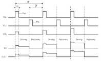
이 OLED 구동회로(105)의 구동 파형은 도 6에서 보는 바와 같다. 도 6에서 "1F"는 1 프레임기간, "1H"는 1 수평기간, "Vg_i"는 제i 게이트라인(Gi)으로부터 공급되는 게이트전압, "Psc"는 스캔펄스, "Vd_j"는 제j 데이터라인(Dj)으로부터 공급되는 데이터전압, "Vr_i"는 제i 리셋라인(Ri)으로부터 공급되는 리셋전압(Vr_i), "Prs"는 리셋펄스, "VN1"은 제1 노드(N1) 상의 전압, "IOLED"는 OLED를 통해 흐르는 전류를 나타낸다.The drive waveform of this
도 5 및 도 6을 참조하면, 제1 트랜지스터(T1)는 제i 게이트라인(Gi)을 통해 스캔펄스(Psc)가 공급되면 턴-온되어 제j 데이터라인(Dj)으로부터 공급된 데이터 전압(Vd)을 제1 노드(N1)에 공급한다. 제1 노드(N1)에 공급된 데이터 전압(Vd)은 제2 트랜지스터(T2)의 게이트단자로 공급된다. 이와 같이 공급되는 데이터 전압(Vd)에 의해 제2 트랜지스터(T2)가 턴-온되면, OLED를 통해 전류가 흐르게 된다. 이 때, OLED를 통해 흐르는 전류는 고전위 전원전압(Vdd)에 의해 발생되며, 그 전류량은 제2 트랜지스터(T2)의 게이트전극에 인가되는 데이터 전압(Vd)의 크기에 비례한다. 그리고, 제1 트랜지스터(T1)가 턴-오프 되어도 데이터 전압(Vd)에 의한 제1 노드(N1) 상의 전압(VN1)은 리셋펄스(Prs)에 의해 제3 트랜지스터(T3)가 가 턴-온되어 제1 노드(N1)가 방전될 때까지 유지한다. 따라서, 제2 트랜지스터(T2)도 리셋펄스(Prs)가 공급될 때 까지 턴-온 상태를 유지한다. 이 때, 제i 리셋라인(Ri)으로부터 공급되는 리셋펄스(Prs)는 프레임기간마다 스캔펄스(Psc)와 1/2 프레임기간의 시간차를 두고 발생한다.5 and 6, when the scan pulse Psc is supplied through the i-th gate line Gi, the first transistor T1 is turned on to supply a data voltage supplied from the j-th data line Dj. Vd) is supplied to the first node N1. The data voltage Vd supplied to the first node N1 is supplied to the gate terminal of the second transistor T2. When the second transistor T2 is turned on by the data voltage Vd supplied as above, current flows through the OLED. At this time, a current flowing through the OLED is generated by the high potential power voltage Vdd, and the amount of current is proportional to the magnitude of the data voltage Vd applied to the gate electrode of the second transistor T2. Also, even when the first transistor T1 is turned off, the voltage VN1 on the first node N1 due to the data voltage Vd is turned on by the reset pulse Prs. It is turned on and maintained until the first node N1 is discharged. Therefore, the second transistor T2 also remains turned on until the reset pulse Prs is supplied. At this time, the reset pulse Prs supplied from the i-th reset line Ri is generated with a time difference between the scan pulse Psc and the half frame period for each frame period.
이와 같이 스캔펄스(Psc)와 1/2 프레임기간의 시간차를 두고 발생하는 리셋펄스(Prs)에 의해 제3 트랜지스터(T3)를 이용하여 제1 노드(N1)을 방전시킴으로써, 제2 트랜지스터(T2)는 1/2 프레임기간 동안의 회복 기간을 가지게 된다. 즉, 도 7에서 보는 바와 같이 1/2 프레임기간의 턴-온 기간 동안 제2 트랜지스터(T2)에 누적되어 증가하는 게이트-바이어스 스트레스는 턴-오프 되는 1/2 프레임기간 감소하게된다.As described above, the second node T2 is discharged by discharging the first node N1 using the third transistor T3 by the reset pulse Prs generated with a time difference between the scan pulse Psc and the half frame period. ) Has a recovery period for 1/2 frame period. That is, as shown in FIG. 7, the gate-biased stress accumulated in the second transistor T2 during the turn-on period of the half frame period is reduced by the half-frame period turned off.
정리하면, 제2 트랜지스터(T2), 즉 OLED 구동 소자는 1/2 프레임 기간 동안 턴-온 상태를 유지한 후, 1/2 프레임 기간 동안에는 턴-오프 상태를 유지한다. 따라서, 턴-온 상태일 때 발생한 OLED 구동 소자의 특성변화는 턴-오프 상태일 때 회복되므로, OLED 구동 소자의 열화에 의한 특성변화를 방지하여 OLED 구동회로의 동작에 대한 신뢰성을 향상시킬 수 있다.In summary, the second transistor T2, that is, the OLED driving element, is turned on for the half frame period, and then is turned off for the half frame period. Therefore, since the characteristic change of the OLED driving element generated during the turn-on state is recovered during the turn-off state, it is possible to improve the reliability of the operation of the OLED driving circuit by preventing the characteristic change caused by the degradation of the OLED driving element. .
도 8의 (a)와 (b)는 기 제안된 도 6의 OLED 구동회로 구동 파형과 이에 비하여 회복 효과를 크게 하여 신뢰성을 강화한 경우의 구동 파형을 나타낸다. 두 경우의 차이는 게이트전압(Vg_i)과 리셋전압(Vr_i) 저전위 기준전압을 데이터 전압 (Vd_j)의 저전위 기준전압보다 낮게 구동하는 것을 특징으로 한다. 도 8의 (a)의 경우에는 반주기 구동에 의하여 구동에 따른 포지티브 바이어스 스트레스를 다음 반주기 동안 회복하여 신뢰성을 향상시킨다. 그러나 신뢰성 향상을 위한 회복 구간 동안 OLED 구동소자(제2 트랜지스터)의 게이트전극에는 소스전극과 같은 전압이 인가된다. 물론 이 경우에도 회복 효과가 있으며, 이에 따라 신뢰성을 향상시킬 수 있다. 그러나 회복 구간 동안 OLED 구동소자의 게이트 전극에 소스 및 데이터전극 보다 상대적으로 낮은 전원을 인가하는 경우에는 네가티브 바이어스 스트레스 효과를 더욱 크게 할 수 있다. 즉 네가티브 바이어스 스트레스 효과를 더욱 크게 하여, OLED 구동소자의 특성 회복을 크게 할 수 있다. 일반적으로 게이트-바이어스 스트레스는 인가된 전압의 크기에 비례적이며, 이에 따라 OLED 구동소자의 저전위 기준전압보다 낮은 제2 저전위 기준전압을 이용하여 네가티브 바이어스 스트레스 효과를 강화하여 전체적으로 구동에 따른 특성 변화에 의한 신뢰성을 크게 향상 시킬 수 있다.8 (a) and 8 (b) show the driving waveforms of the OLED driving circuit driving waveform of FIG. 6 which has been previously proposed and the case where the reliability is enhanced by increasing the recovery effect. The difference between the two cases is characterized in that the low voltage reference voltage of the gate voltage Vg_i and the reset voltage Vr_i is driven to be lower than the low voltage reference voltage of the data voltage Vd_j. In the case of FIG. 8A, the positive bias stress caused by the driving is recovered during the next half cycle by the half cycle driving, thereby improving reliability. However, the same voltage as the source electrode is applied to the gate electrode of the OLED driving device (second transistor) during the recovery period for improving the reliability. Of course, even in this case, there is a recovery effect, thereby improving the reliability. However, when a relatively lower power source is applied to the gate electrode of the OLED driving device than the source and data electrodes during the recovery period, the negative bias stress effect can be increased. In other words, the negative bias stress effect can be further increased, and the characteristic recovery of the OLED driving device can be increased. In general, the gate-biased stress is proportional to the magnitude of the applied voltage. Accordingly, the negative bias stress effect is enhanced by using the second low potential reference voltage lower than the low potential reference voltage of the OLED driving device, and thus the characteristics of the overall driving characteristics. The reliability by change can be greatly improved.
도 8의 (b)에 네가티브 바이어스 스트레스를 강화하여 회복 특성을 향상시키기 위한 새로운 구동 파형을 나타내었다. 이 구동 파형은 게이트전압(Vg_i) 파형과 리셋전압(Vr_i) 파형의 저전위 기준전압이 데이터 전압(Vd_g)의 저전위 기준전압보다 낮은 것을 특징으로 한다. 도 8에 나타낸 바와 같이 OLED 구동소자의 제어노드(제1 노드)에 인가되는 누적 바이어스 스트레스는 빗금친 영역과 비례적이라고 한다면, 도 8의 (b)와 같이 구동하는 경우, 누적 바이어스 스트레스를 최소화 하여 특성 변화를 최소화 할 수 있다. 또한 데이터 전압(Vd_g)의 저전위 기준전압에 비 하여 상대적으로 낮은 제2 저전위 기준전압(즉, 게이트전압 과 리셋전압의 저전위 기준전압)의 조절을 통하여 네가티브 바이어스 스트레스의 크기를 조절 할 수 있으며, 이를 통하여 누적 바이어스 스트레스를 최소화 할 수 있다.8 (b) shows a new driving waveform for enhancing the negative bias stress to improve the recovery characteristics. The driving waveform is characterized in that the low potential reference voltage of the gate voltage Vg_i waveform and the reset voltage Vr_i waveform is lower than the low potential reference voltage of the data voltage Vd_g. As shown in FIG. 8, if the cumulative bias stress applied to the control node (first node) of the OLED driving element is proportional to the hatched area, the cumulative bias stress is minimized when driving as shown in FIG. 8B. It can minimize the change of characteristics. In addition, the magnitude of the negative bias stress can be adjusted by adjusting the second low potential reference voltage (that is, the low potential reference voltage of the gate voltage and the reset voltage) that is relatively lower than the low potential reference voltage of the data voltage Vd_g. Through this, cumulative bias stress can be minimized.
상술한 바와 같이, 본 발명의 실시예에 따른 OLED 구동회로는 리셋펄스에 응답하여 OLED 구동소자의 제어노드를 방전시키는 제3 트랜지스터를 구비하여 OLED 구동소자의 열화에 의한 특성변화를 방지할 수 있어 동작의 신뢰성이 향상된다. 아울러 데이터 전압의 저전위 기준전압보다 스캔펄스 및 리셋펄스의 저전위 기준전압을 낮게 하는 구동 파형을 공급하여 더욱 향상된 OLED 구동회로 동작의 신뢰성을 확보할 수 있다.As described above, the OLED driving circuit according to the embodiment of the present invention includes a third transistor for discharging the control node of the OLED driving element in response to the reset pulse to prevent the characteristic change due to degradation of the OLED driving element The reliability of the operation is improved. In addition, it is possible to secure a more reliable OLED driving circuit operation by supplying a driving waveform that lowers the low potential reference voltage of the scan pulse and the reset pulse than the low potential reference voltage of the data voltage.
이상 설명한 내용을 통해 당업자라면 본 발명의 기술사상을 일탈하지 아니하는 범위에서 다양한 변경 및 수정이 가능함을 알 수 있을 것이다. 따라서, 본 발명의 기술적 범위는 명세서의 상세한 설명에 기재된 내용으로 한정되는 것이 아니라 특허 청구의 범위에 의해 정하여져야만 할 것이다.It will be apparent to those skilled in the art that various modifications and variations can be made in the present invention without departing from the spirit or scope of the invention. Therefore, the technical scope of the present invention should not be limited to the contents described in the detailed description of the specification but should be defined by the claims.
Claims (12)
Translated fromKoreanPriority Applications (4)
| Application Number | Priority Date | Filing Date | Title |
|---|---|---|---|
| KR1020050053120AKR101157979B1 (en) | 2005-06-20 | 2005-06-20 | Driving Circuit for Organic Light Emitting Diode and Organic Light Emitting Diode Display Using The Same |
| CNB2005101141173ACN100565644C (en) | 2005-06-20 | 2005-10-17 | The driving circuit of Organic Light Emitting Diode and use the display of this driving circuit |
| US11/292,873US7675493B2 (en) | 2005-06-20 | 2005-12-02 | Driving circuit for organic light emitting diode, display device using the same and driving method of organic light emitting diode display device |
| JP2005364023AJP5236156B2 (en) | 2005-06-20 | 2005-12-16 | Organic light emitting diode display |
Applications Claiming Priority (1)
| Application Number | Priority Date | Filing Date | Title |
|---|---|---|---|
| KR1020050053120AKR101157979B1 (en) | 2005-06-20 | 2005-06-20 | Driving Circuit for Organic Light Emitting Diode and Organic Light Emitting Diode Display Using The Same |
Publications (2)
| Publication Number | Publication Date |
|---|---|
| KR20060133321A KR20060133321A (en) | 2006-12-26 |
| KR101157979B1true KR101157979B1 (en) | 2012-06-25 |
Family
ID=37572853
Family Applications (1)
| Application Number | Title | Priority Date | Filing Date |
|---|---|---|---|
| KR1020050053120AExpired - LifetimeKR101157979B1 (en) | 2005-06-20 | 2005-06-20 | Driving Circuit for Organic Light Emitting Diode and Organic Light Emitting Diode Display Using The Same |
Country Status (4)
| Country | Link |
|---|---|
| US (1) | US7675493B2 (en) |
| JP (1) | JP5236156B2 (en) |
| KR (1) | KR101157979B1 (en) |
| CN (1) | CN100565644C (en) |
Families Citing this family (93)
| Publication number | Priority date | Publication date | Assignee | Title |
|---|---|---|---|---|
| US7569849B2 (en) | 2001-02-16 | 2009-08-04 | Ignis Innovation Inc. | Pixel driver circuit and pixel circuit having the pixel driver circuit |
| CA2419704A1 (en) | 2003-02-24 | 2004-08-24 | Ignis Innovation Inc. | Method of manufacturing a pixel with organic light-emitting diode |
| CA2443206A1 (en) | 2003-09-23 | 2005-03-23 | Ignis Innovation Inc. | Amoled display backplanes - pixel driver circuits, array architecture, and external compensation |
| CA2472671A1 (en) | 2004-06-29 | 2005-12-29 | Ignis Innovation Inc. | Voltage-programming scheme for current-driven amoled displays |
| CA2490858A1 (en) | 2004-12-07 | 2006-06-07 | Ignis Innovation Inc. | Driving method for compensated voltage-programming of amoled displays |
| US8576217B2 (en) | 2011-05-20 | 2013-11-05 | Ignis Innovation Inc. | System and methods for extraction of threshold and mobility parameters in AMOLED displays |
| TWI402790B (en) | 2004-12-15 | 2013-07-21 | Ignis Innovation Inc | Method and system for programming, calibrating and driving a light-emitting element display |
| US10012678B2 (en) | 2004-12-15 | 2018-07-03 | Ignis Innovation Inc. | Method and system for programming, calibrating and/or compensating, and driving an LED display |
| US9280933B2 (en) | 2004-12-15 | 2016-03-08 | Ignis Innovation Inc. | System and methods for extraction of threshold and mobility parameters in AMOLED displays |
| US9275579B2 (en) | 2004-12-15 | 2016-03-01 | Ignis Innovation Inc. | System and methods for extraction of threshold and mobility parameters in AMOLED displays |
| US10013907B2 (en) | 2004-12-15 | 2018-07-03 | Ignis Innovation Inc. | Method and system for programming, calibrating and/or compensating, and driving an LED display |
| US9799246B2 (en) | 2011-05-20 | 2017-10-24 | Ignis Innovation Inc. | System and methods for extraction of threshold and mobility parameters in AMOLED displays |
| US20140111567A1 (en) | 2005-04-12 | 2014-04-24 | Ignis Innovation Inc. | System and method for compensation of non-uniformities in light emitting device displays |
| US9171500B2 (en) | 2011-05-20 | 2015-10-27 | Ignis Innovation Inc. | System and methods for extraction of parasitic parameters in AMOLED displays |
| CA2495726A1 (en) | 2005-01-28 | 2006-07-28 | Ignis Innovation Inc. | Locally referenced voltage programmed pixel for amoled displays |
| CA2496642A1 (en) | 2005-02-10 | 2006-08-10 | Ignis Innovation Inc. | Fast settling time driving method for organic light-emitting diode (oled) displays based on current programming |
| JP5355080B2 (en) | 2005-06-08 | 2013-11-27 | イグニス・イノベイション・インコーポレーテッド | Method and system for driving a light emitting device display |
| CA2518276A1 (en) | 2005-09-13 | 2007-03-13 | Ignis Innovation Inc. | Compensation technique for luminance degradation in electro-luminance devices |
| TW200746022A (en)* | 2006-04-19 | 2007-12-16 | Ignis Innovation Inc | Stable driving scheme for active matrix displays |
| US7642997B2 (en)* | 2006-06-28 | 2010-01-05 | Eastman Kodak Company | Active matrix display compensation |
| CA2556961A1 (en) | 2006-08-15 | 2008-02-15 | Ignis Innovation Inc. | Oled compensation technique based on oled capacitance |
| JP5414161B2 (en)* | 2007-08-10 | 2014-02-12 | キヤノン株式会社 | Thin film transistor circuit, light emitting display device, and driving method thereof |
| US8004479B2 (en)* | 2007-11-28 | 2011-08-23 | Global Oled Technology Llc | Electroluminescent display with interleaved 3T1C compensation |
| KR101338312B1 (en)* | 2008-04-30 | 2013-12-09 | 엘지디스플레이 주식회사 | Organic electroluminescent display device and driving method thereof |
| US9384698B2 (en) | 2009-11-30 | 2016-07-05 | Ignis Innovation Inc. | System and methods for aging compensation in AMOLED displays |
| CA2688870A1 (en) | 2009-11-30 | 2011-05-30 | Ignis Innovation Inc. | Methode and techniques for improving display uniformity |
| US9311859B2 (en) | 2009-11-30 | 2016-04-12 | Ignis Innovation Inc. | Resetting cycle for aging compensation in AMOLED displays |
| CA2669367A1 (en) | 2009-06-16 | 2010-12-16 | Ignis Innovation Inc | Compensation technique for color shift in displays |
| US10319307B2 (en) | 2009-06-16 | 2019-06-11 | Ignis Innovation Inc. | Display system with compensation techniques and/or shared level resources |
| JP5321304B2 (en)* | 2009-07-14 | 2013-10-23 | ソニー株式会社 | Display device, driving method thereof, and electronic apparatus |
| US8497828B2 (en) | 2009-11-12 | 2013-07-30 | Ignis Innovation Inc. | Sharing switch TFTS in pixel circuits |
| US10996258B2 (en) | 2009-11-30 | 2021-05-04 | Ignis Innovation Inc. | Defect detection and correction of pixel circuits for AMOLED displays |
| US8803417B2 (en) | 2009-12-01 | 2014-08-12 | Ignis Innovation Inc. | High resolution pixel architecture |
| CA2687631A1 (en) | 2009-12-06 | 2011-06-06 | Ignis Innovation Inc | Low power driving scheme for display applications |
| US9881532B2 (en) | 2010-02-04 | 2018-01-30 | Ignis Innovation Inc. | System and method for extracting correlation curves for an organic light emitting device |
| US10176736B2 (en) | 2010-02-04 | 2019-01-08 | Ignis Innovation Inc. | System and methods for extracting correlation curves for an organic light emitting device |
| CA2692097A1 (en) | 2010-02-04 | 2011-08-04 | Ignis Innovation Inc. | Extracting correlation curves for light emitting device |
| US10163401B2 (en) | 2010-02-04 | 2018-12-25 | Ignis Innovation Inc. | System and methods for extracting correlation curves for an organic light emitting device |
| US10089921B2 (en) | 2010-02-04 | 2018-10-02 | Ignis Innovation Inc. | System and methods for extracting correlation curves for an organic light emitting device |
| US20140313111A1 (en) | 2010-02-04 | 2014-10-23 | Ignis Innovation Inc. | System and methods for extracting correlation curves for an organic light emitting device |
| CA2696778A1 (en) | 2010-03-17 | 2011-09-17 | Ignis Innovation Inc. | Lifetime, uniformity, parameter extraction methods |
| WO2012002199A1 (en)* | 2010-06-28 | 2012-01-05 | シャープ株式会社 | Active matrix substrate, display device, and method for testing the active matrix substrate or the display device |
| US8907991B2 (en) | 2010-12-02 | 2014-12-09 | Ignis Innovation Inc. | System and methods for thermal compensation in AMOLED displays |
| US9606607B2 (en) | 2011-05-17 | 2017-03-28 | Ignis Innovation Inc. | Systems and methods for display systems with dynamic power control |
| CN109272933A (en) | 2011-05-17 | 2019-01-25 | 伊格尼斯创新公司 | The method for operating display |
| US8581625B2 (en) | 2011-05-19 | 2013-11-12 | Semiconductor Energy Laboratory Co., Ltd. | Programmable logic device |
| US9530349B2 (en) | 2011-05-20 | 2016-12-27 | Ignis Innovations Inc. | Charged-based compensation and parameter extraction in AMOLED displays |
| US9466240B2 (en) | 2011-05-26 | 2016-10-11 | Ignis Innovation Inc. | Adaptive feedback system for compensating for aging pixel areas with enhanced estimation speed |
| US9773439B2 (en) | 2011-05-27 | 2017-09-26 | Ignis Innovation Inc. | Systems and methods for aging compensation in AMOLED displays |
| TWI441137B (en) | 2011-07-08 | 2014-06-11 | Hannstar Display Corp | Compensation circuit for keeping luminance intensity of diode |
| US9070775B2 (en) | 2011-08-03 | 2015-06-30 | Ignis Innovations Inc. | Thin film transistor |
| US8901579B2 (en) | 2011-08-03 | 2014-12-02 | Ignis Innovation Inc. | Organic light emitting diode and method of manufacturing |
| US9324268B2 (en) | 2013-03-15 | 2016-04-26 | Ignis Innovation Inc. | Amoled displays with multiple readout circuits |
| US9385169B2 (en) | 2011-11-29 | 2016-07-05 | Ignis Innovation Inc. | Multi-functional active matrix organic light-emitting diode display |
| US10089924B2 (en) | 2011-11-29 | 2018-10-02 | Ignis Innovation Inc. | Structural and low-frequency non-uniformity compensation |
| KR101368244B1 (en) | 2011-12-30 | 2014-02-28 | 주식회사 실리콘웍스 | Circuit for sensing threshold voltage of organic light emitting diode display device |
| US8937632B2 (en) | 2012-02-03 | 2015-01-20 | Ignis Innovation Inc. | Driving system for active-matrix displays |
| KR101939233B1 (en)* | 2012-05-11 | 2019-04-10 | 엘지디스플레이 주식회사 | Image display device and method of driving the same |
| US9747834B2 (en) | 2012-05-11 | 2017-08-29 | Ignis Innovation Inc. | Pixel circuits including feedback capacitors and reset capacitors, and display systems therefore |
| US8922544B2 (en) | 2012-05-23 | 2014-12-30 | Ignis Innovation Inc. | Display systems with compensation for line propagation delay |
| US9336717B2 (en) | 2012-12-11 | 2016-05-10 | Ignis Innovation Inc. | Pixel circuits for AMOLED displays |
| US9786223B2 (en) | 2012-12-11 | 2017-10-10 | Ignis Innovation Inc. | Pixel circuits for AMOLED displays |
| CN108665836B (en) | 2013-01-14 | 2021-09-03 | 伊格尼斯创新公司 | Method and system for compensating for deviations of a measured device current from a reference current |
| US9830857B2 (en) | 2013-01-14 | 2017-11-28 | Ignis Innovation Inc. | Cleaning common unwanted signals from pixel measurements in emissive displays |
| US9721505B2 (en) | 2013-03-08 | 2017-08-01 | Ignis Innovation Inc. | Pixel circuits for AMOLED displays |
| EP3043338A1 (en) | 2013-03-14 | 2016-07-13 | Ignis Innovation Inc. | Re-interpolation with edge detection for extracting an aging pattern for amoled displays |
| US9952698B2 (en) | 2013-03-15 | 2018-04-24 | Ignis Innovation Inc. | Dynamic adjustment of touch resolutions on an AMOLED display |
| WO2014174427A1 (en) | 2013-04-22 | 2014-10-30 | Ignis Innovation Inc. | Inspection system for oled display panels |
| CN105474296B (en) | 2013-08-12 | 2017-08-18 | 伊格尼斯创新公司 | A method and device for driving a display using image data |
| KR102071298B1 (en)* | 2013-09-30 | 2020-03-02 | 주식회사 실리콘웍스 | Sample and hold circuit and source driver having the same |
| US9741282B2 (en) | 2013-12-06 | 2017-08-22 | Ignis Innovation Inc. | OLED display system and method |
| US9761170B2 (en) | 2013-12-06 | 2017-09-12 | Ignis Innovation Inc. | Correction for localized phenomena in an image array |
| US10839734B2 (en)* | 2013-12-23 | 2020-11-17 | Universal Display Corporation | OLED color tuning by driving mode variation |
| US9502653B2 (en) | 2013-12-25 | 2016-11-22 | Ignis Innovation Inc. | Electrode contacts |
| US10997901B2 (en) | 2014-02-28 | 2021-05-04 | Ignis Innovation Inc. | Display system |
| US10176752B2 (en) | 2014-03-24 | 2019-01-08 | Ignis Innovation Inc. | Integrated gate driver |
| DE102015206281A1 (en) | 2014-04-08 | 2015-10-08 | Ignis Innovation Inc. | Display system with shared level resources for portable devices |
| CA2872563A1 (en) | 2014-11-28 | 2016-05-28 | Ignis Innovation Inc. | High pixel density array architecture |
| CA2879462A1 (en) | 2015-01-23 | 2016-07-23 | Ignis Innovation Inc. | Compensation for color variation in emissive devices |
| CA2889870A1 (en) | 2015-05-04 | 2016-11-04 | Ignis Innovation Inc. | Optical feedback system |
| CA2892714A1 (en) | 2015-05-27 | 2016-11-27 | Ignis Innovation Inc | Memory bandwidth reduction in compensation system |
| US10373554B2 (en) | 2015-07-24 | 2019-08-06 | Ignis Innovation Inc. | Pixels and reference circuits and timing techniques |
| US10657895B2 (en) | 2015-07-24 | 2020-05-19 | Ignis Innovation Inc. | Pixels and reference circuits and timing techniques |
| CA2898282A1 (en) | 2015-07-24 | 2017-01-24 | Ignis Innovation Inc. | Hybrid calibration of current sources for current biased voltage progra mmed (cbvp) displays |
| CA2900170A1 (en) | 2015-08-07 | 2017-02-07 | Gholamreza Chaji | Calibration of pixel based on improved reference values |
| CA2909813A1 (en) | 2015-10-26 | 2017-04-26 | Ignis Innovation Inc | High ppi pattern orientation |
| US10586491B2 (en) | 2016-12-06 | 2020-03-10 | Ignis Innovation Inc. | Pixel circuits for mitigation of hysteresis |
| US10714018B2 (en) | 2017-05-17 | 2020-07-14 | Ignis Innovation Inc. | System and method for loading image correction data for displays |
| US11025899B2 (en) | 2017-08-11 | 2021-06-01 | Ignis Innovation Inc. | Optical correction systems and methods for correcting non-uniformity of emissive display devices |
| US10971078B2 (en) | 2018-02-12 | 2021-04-06 | Ignis Innovation Inc. | Pixel measurement through data line |
| CN110021261B (en)* | 2018-06-28 | 2020-11-03 | 京东方科技集团股份有限公司 | Array substrate and driving method thereof, and display panel |
| KR102691216B1 (en)* | 2018-10-26 | 2024-08-05 | 삼성디스플레이 주식회사 | Display device and electronic device having the same |
| US11488533B2 (en) | 2021-08-03 | 2022-11-01 | Google Llc | Delaying anode voltage reset for quicker response times in OLED displays |
Citations (1)
| Publication number | Priority date | Publication date | Assignee | Title |
|---|---|---|---|---|
| JP2004102278A (en)* | 2002-08-28 | 2004-04-02 | Au Optronics Corp | Driving circuit and driving method for light emitting device |
Family Cites Families (8)
| Publication number | Priority date | Publication date | Assignee | Title |
|---|---|---|---|---|
| JP4092857B2 (en) | 1999-06-17 | 2008-05-28 | ソニー株式会社 | Image display device |
| JP3877049B2 (en)* | 2000-06-27 | 2007-02-07 | 株式会社日立製作所 | Image display apparatus and driving method thereof |
| JP4731718B2 (en)* | 2001-04-27 | 2011-07-27 | 株式会社半導体エネルギー研究所 | Display device |
| TW589597B (en)* | 2002-07-24 | 2004-06-01 | Au Optronics Corp | Driving method and system for a light emitting device |
| JP2004118132A (en)* | 2002-09-30 | 2004-04-15 | Hitachi Ltd | DC current display |
| JP2004341144A (en)* | 2003-05-15 | 2004-12-02 | Hitachi Ltd | Image display device |
| CN100363966C (en) | 2004-07-07 | 2008-01-23 | 友达光电股份有限公司 | Pixel driving circuit of voltage-driven active organic light-emitting display |
| US7116058B2 (en)* | 2004-11-30 | 2006-10-03 | Wintek Corporation | Method of improving the stability of active matrix OLED displays driven by amorphous silicon thin-film transistors |
- 2005
- 2005-06-20KRKR1020050053120Apatent/KR101157979B1/ennot_activeExpired - Lifetime
- 2005-10-17CNCNB2005101141173Apatent/CN100565644C/ennot_activeExpired - Lifetime
- 2005-12-02USUS11/292,873patent/US7675493B2/enactiveActive
- 2005-12-16JPJP2005364023Apatent/JP5236156B2/enactiveActive
Patent Citations (1)
| Publication number | Priority date | Publication date | Assignee | Title |
|---|---|---|---|---|
| JP2004102278A (en)* | 2002-08-28 | 2004-04-02 | Au Optronics Corp | Driving circuit and driving method for light emitting device |
Also Published As
| Publication number | Publication date |
|---|---|
| JP5236156B2 (en) | 2013-07-17 |
| US7675493B2 (en) | 2010-03-09 |
| KR20060133321A (en) | 2006-12-26 |
| CN1885394A (en) | 2006-12-27 |
| JP2007004114A (en) | 2007-01-11 |
| US20060284801A1 (en) | 2006-12-21 |
| CN100565644C (en) | 2009-12-02 |
Similar Documents
| Publication | Publication Date | Title |
|---|---|---|
| KR101157979B1 (en) | Driving Circuit for Organic Light Emitting Diode and Organic Light Emitting Diode Display Using The Same | |
| KR101169053B1 (en) | Organic Light Emitting Diode Display | |
| JP4630789B2 (en) | Light emitting display device and pixel circuit | |
| KR100673760B1 (en) | Light emitting display | |
| KR101186254B1 (en) | Organic Light Emitting Diode Display And Driving Method Thereof | |
| JP4170384B2 (en) | Self-luminous display device | |
| JP5157467B2 (en) | Self-luminous display device and driving method thereof | |
| JP3570394B2 (en) | Active matrix type display device, active matrix type organic electroluminescence display device, and driving method thereof | |
| US7609234B2 (en) | Pixel circuit and driving method for active matrix organic light-emitting diodes, and display using the same | |
| US7679587B2 (en) | Pixel circuit and light emitting display using the same | |
| KR100568597B1 (en) | Electro-luminescence display and its driving method | |
| KR100568592B1 (en) | Electro-luminescence display and its driving method | |
| KR100628277B1 (en) | Organic light emitting display device and driving method thereof | |
| KR101184065B1 (en) | Organic Light Emitting Diode Display | |
| KR20080113998A (en) | Active matrix organic light emitting display device and driving method thereof | |
| JP5789585B2 (en) | Display device and electronic device | |
| KR101137849B1 (en) | A light emitting display device | |
| KR101474023B1 (en) | Organic light emitting diode display device | |
| KR100595108B1 (en) | Pixel and light emitting display device and driving method thereof | |
| KR101483967B1 (en) | Circuit of voltage compensation and control method thereof | |
| KR101519445B1 (en) | Circuit of voltage compensation and control method thereof | |
| KR100692854B1 (en) | Method and apparatus for driving electro-luminescence display panel | |
| KR100555310B1 (en) | Electro-luminescence display and its driving method | |
| KR100923353B1 (en) | Electro-luminescence display and its driving method | |
| KR100511787B1 (en) | Apparatus and method for driving electro-luminescence display panel |
Legal Events
| Date | Code | Title | Description |
|---|---|---|---|
| PA0109 | Patent application | Patent event code:PA01091R01D Comment text:Patent Application Patent event date:20050620 | |
| PG1501 | Laying open of application | ||
| A201 | Request for examination | ||
| PA0201 | Request for examination | Patent event code:PA02012R01D Patent event date:20100609 Comment text:Request for Examination of Application Patent event code:PA02011R01I Patent event date:20050620 Comment text:Patent Application | |
| E902 | Notification of reason for refusal | ||
| PE0902 | Notice of grounds for rejection | Comment text:Notification of reason for refusal Patent event date:20111025 Patent event code:PE09021S01D | |
| E701 | Decision to grant or registration of patent right | ||
| PE0701 | Decision of registration | Patent event code:PE07011S01D Comment text:Decision to Grant Registration Patent event date:20120523 | |
| GRNT | Written decision to grant | ||
| PR0701 | Registration of establishment | Comment text:Registration of Establishment Patent event date:20120613 Patent event code:PR07011E01D | |
| PR1002 | Payment of registration fee | Payment date:20120614 End annual number:3 Start annual number:1 | |
| PG1601 | Publication of registration | ||
| FPAY | Annual fee payment | Payment date:20150528 Year of fee payment:4 | |
| PR1001 | Payment of annual fee | Payment date:20150528 Start annual number:4 End annual number:4 | |
| FPAY | Annual fee payment | Payment date:20160530 Year of fee payment:5 | |
| PR1001 | Payment of annual fee | Payment date:20160530 Start annual number:5 End annual number:5 | |
| FPAY | Annual fee payment | Payment date:20180515 Year of fee payment:7 | |
| PR1001 | Payment of annual fee | Payment date:20180515 Start annual number:7 End annual number:7 | |
| FPAY | Annual fee payment | Payment date:20190515 Year of fee payment:8 | |
| PR1001 | Payment of annual fee | Payment date:20190515 Start annual number:8 End annual number:8 | |
| PR1001 | Payment of annual fee | Payment date:20200513 Start annual number:9 End annual number:9 | |
| PR1001 | Payment of annual fee | Payment date:20210511 Start annual number:10 End annual number:10 | |
| PR1001 | Payment of annual fee | Payment date:20220516 Start annual number:11 End annual number:11 | |
| PR1001 | Payment of annual fee | Payment date:20230515 Start annual number:12 End annual number:12 |