KR101157659B1 - Manufacture Method of Organic Light Emitting Diodes Using Porous Substrate - Google Patents
Manufacture Method of Organic Light Emitting Diodes Using Porous SubstrateDownload PDFInfo
- Publication number
- KR101157659B1 KR101157659B1KR1020090092528AKR20090092528AKR101157659B1KR 101157659 B1KR101157659 B1KR 101157659B1KR 1020090092528 AKR1020090092528 AKR 1020090092528AKR 20090092528 AKR20090092528 AKR 20090092528AKR 101157659 B1KR101157659 B1KR 101157659B1
- Authority
- KR
- South Korea
- Prior art keywords
- light emitting
- organic light
- porous substrate
- emitting device
- substrate
- Prior art date
- Legal status (The legal status is an assumption and is not a legal conclusion. Google has not performed a legal analysis and makes no representation as to the accuracy of the status listed.)
- Expired - Fee Related
Links
Images


Classifications
- H—ELECTRICITY
- H10—SEMICONDUCTOR DEVICES; ELECTRIC SOLID-STATE DEVICES NOT OTHERWISE PROVIDED FOR
- H10K—ORGANIC ELECTRIC SOLID-STATE DEVICES
- H10K77/00—Constructional details of devices covered by this subclass and not covered by groups H10K10/80, H10K30/80, H10K50/80 or H10K59/80
- H10K77/10—Substrates, e.g. flexible substrates
- H—ELECTRICITY
- H10—SEMICONDUCTOR DEVICES; ELECTRIC SOLID-STATE DEVICES NOT OTHERWISE PROVIDED FOR
- H10K—ORGANIC ELECTRIC SOLID-STATE DEVICES
- H10K71/00—Manufacture or treatment specially adapted for the organic devices covered by this subclass
- H10K71/10—Deposition of organic active material
- Y—GENERAL TAGGING OF NEW TECHNOLOGICAL DEVELOPMENTS; GENERAL TAGGING OF CROSS-SECTIONAL TECHNOLOGIES SPANNING OVER SEVERAL SECTIONS OF THE IPC; TECHNICAL SUBJECTS COVERED BY FORMER USPC CROSS-REFERENCE ART COLLECTIONS [XRACs] AND DIGESTS
- Y02—TECHNOLOGIES OR APPLICATIONS FOR MITIGATION OR ADAPTATION AGAINST CLIMATE CHANGE
- Y02E—REDUCTION OF GREENHOUSE GAS [GHG] EMISSIONS, RELATED TO ENERGY GENERATION, TRANSMISSION OR DISTRIBUTION
- Y02E10/00—Energy generation through renewable energy sources
- Y02E10/50—Photovoltaic [PV] energy
- Y02E10/549—Organic PV cells
Landscapes
- Engineering & Computer Science (AREA)
- Manufacturing & Machinery (AREA)
- Electroluminescent Light Sources (AREA)
Abstract
Translated fromKoreanDescription
Translated fromKorean본 발명은 다공성 기판을 이용한 유기발광소자의 제조 방법에 관한 것이다.The present invention relates to a method of manufacturing an organic light emitting device using a porous substrate.
유기발광소자(OLED; Organic Light Emitting Diodes)는 얇고 가벼우며 낮은 전력 소모, 높은 휘도, 빠른 응답 속도 등의 장점이 있어 주목 받고 있는 디스플레이이다. 이 같이 많은 장점이 있는 유기발광소자도 고해상도 고효율 대면적 구현, 플렉시블(Flexible) 유기발광소자 개발, 경제성 향상과 같은 몇 가지 해결 해야 할 과제를 갖고 있다.Organic Light Emitting Diodes (OLEDs) are attracting attention because of their thin, light, low power consumption, high brightness, and fast response speed. Such organic light emitting diodes, which have many advantages, have some problems to be solved, such as high-resolution high-efficiency large area, flexible organic light-emitting diode development, and economical improvement.
먼저, 고효율, 대면적 유기발광소자 구현을 위해서는 박막 트랜지스터(TFTs; Thin Film Transistors)의 특성을 유기발광소자에 적합하게 향상시키는 방법이 필요하다.First, in order to realize a high efficiency and large area organic light emitting diode, a method of improving the characteristics of thin film transistors (TFTs) is appropriate for an organic light emitting diode.
다음은 유기발광소자용 TFT의 특성 향상이 필요한 이론적, 기술적 배경과 TFT의 종류, 공정 방법에 대한 설명이다.The following is a description of the theoretical and technical background, the types of TFTs, and the process method for improving the characteristics of TFTs for organic light emitting diodes.
유기발광소자는 구동방식에 따라 수동형 유기발광소자(PMOLED; Passive Matrix Organic Light Emitting Diodes)와 능동형 유기발광소자(AMOLED; Active Matrix Organic Light Emitting Diodes)로 나눌 수 있다. 수동형 유기발광소자는 단순한 전극선 배열만으로 화소를 구동 할 수 있어 능동형에 비해 구조가 간단하고 생산비가 저렴한 특징을 갖고 있으나 고해상도와 대면적 디스플레이를 구현하기가 어렵다. 그에 반해 능동형 유기발광소자는 각 화소 마다 박막 트랜지스터를 장착한 구조이기 때문에 화소 각각에 일정한 전류를 공급할 수 있고, 대면적 및 고해상도 구현이 가능하다.The organic light emitting diodes may be classified into passive matrix organic light emitting diodes (PMOLED) and active matrix organic light emitting diodes (AMOLED) according to a driving method. Passive organic light emitting devices can drive pixels with a simple arrangement of electrode lines, which is simpler in structure and lower in production cost than active type, but it is difficult to realize high resolution and large area display. In contrast, the active organic light emitting diode has a structure in which a thin film transistor is mounted in each pixel, so that a constant current can be supplied to each pixel, and a large area and high resolution can be realized.
유기발광소자는 LCD(Liquid Crystal Display)와 달리 전류 구동 방식이기 때문에 TFT의 운반체 이동도(Carrier Mobility)가 높아야 하고, 문턱전압(Threshold Voltage)에 민감하여 안정성과 신뢰성이 중요하다. 또한 유기발광소자가 차세대 디스플레이로 자리잡기 위해서는 고해상도와 대형화가 가능한 TFT가 수반되어야 한다. 이와 같은 요구 조건이 만족되면서 공정이 간단하고 비용 부담이 적어 생산성이 뛰어난 유기발광소자용 TFT개발은 업계의 중요한 과제이다.Unlike the LCD (Liquid Crystal Display), the organic light emitting device is a current driving method, so the carrier mobility of the TFT must be high, and the stability and reliability are important because it is sensitive to the threshold voltage. In addition, in order for an organic light emitting device to become a next-generation display, a high resolution and a large-sized TFT must be accompanied. As these requirements are satisfied, development of TFTs for organic light emitting diodes having excellent productivity due to the simple process and low cost is an important task in the industry.
이러한 능동형 유기발광소자용 TFT는 사용되는 주 재료에 따라 비정질 실리콘(Amorphous-Si / a-Si) TFT, 결정질 실리콘(Poly-Si) TFT, 유기반도체 및 산화물 반도체 TFT로 분류할 수 있다.Such active organic light emitting diode TFTs can be classified into amorphous silicon (Amorphous-Si / a-Si) TFT, crystalline silicon (Poly-Si) TFT, organic semiconductor and oxide semiconductor TFT according to the main material used.
첫째로, 비정질 실리콘 TFT는 공정이 간단하고 대형화가 가능하다는 장점이 있으나, 이동도가 1 cm2/Vs이하로 매우 낮다. 능동형 유기발광소자는 TFT를 통해 전달되는 전류량과 휘도가 비례하기 때문에 이동도가 낮으면 휘도가 감소해 패널 내 에서 균일도를 유지하기 어렵고, 수명도 짧아질 수 있다. 즉, 비정질 실리콘 TFT는 유기발광소자용으로 사용하기에는 많은 문제점을 갖고 있다.Firstly, amorphous silicon TFT has the advantage of simple process and large size, but its mobility is very low below 1 cm2 / Vs. Since the active organic light emitting diode has a luminance proportional to the amount of current transmitted through the TFT, when the mobility is low, the luminance decreases, making it difficult to maintain uniformity in the panel and shortening the lifetime. That is, the amorphous silicon TFT has many problems to be used for the organic light emitting device.
둘째로, 결정질 실리콘 TFT는 이동도가 100cm2/Vs정도로 크고, 집적도가 좋다. 즉, 이동도가 크기 때문에 유기발광소자의 휘도가 높고 발광특성이 안정적이며, 수명이 길어진다. 또한 집적도가 좋아 개구율과 정밀도가 향상되어 고해상도 디스플레이 제조가 가능하다.Secondly, the crystalline silicon TFT has a high mobility of about 100 cm2 / Vs and has good integration. That is, because of the high mobility, the organic light emitting device has high luminance, stable light emission characteristics, and long lifespan. In addition, the high degree of integration improves the aperture ratio and precision, enabling high-resolution displays.
결정질 실리콘TFT는 결정화 방법에 따라 고온다결정실리콘(HTPS; High Temperature Poly Silicon)과, 저온다결정실리콘(LTPS; Low Temperature Poly Silicon)이 있다. HTPS는 1,000℃ 이상의 고온에서 결정화하므로 녹는점이 낮은 유기 기판을 사용할 수 없어서 상대적으로 단가가 높은 석영(Quartz) 기판을 사용해야 한다. 때문에 내열성이 약한 유리 기판에 적용할 수 있는 LTPS의 연구가 활발히 진행 중이다.The crystalline silicon TFT includes high temperature polysilicon (HTPS) and low temperature polysilicon (LTPS) according to a crystallization method. Since HTPS crystallizes at a high temperature of 1,000 ° C. or higher, an organic substrate having a low melting point cannot be used. Therefore, a quartz substrate having a relatively high cost must be used. Therefore, the research of LTPS which can be applied to glass substrates with low heat resistance is actively underway.
LTPS에는 급속 가열 결정화(RTA; Rapid Thermal Annealing)와 같은 열 결정화, 레이저 결정화, CGS(Continuous Grain Silicon)과 같은 복합결정화 방법 등이 있다. 이 같은LTPS 결정화 방법은 500℃ 이하의 저온에서 실리콘을 결정화 하여 TFT를 형성하는 방법으로 내열성이 작은 기판 사용이 용이하다는 장점이 있다. 하지만, LTPS의 저온 공정은 상대적인 개념일 뿐, 500℃ 이상의 온도 상승이 동반되기 때문에 유리 기판의 변형 문제를 완전히 해결하기 어렵고, 플라스틱 기판과 같은 얇고 가벼운 기판 적용이 어렵다. 또한 복잡한 공정, 마스크(Shadow Mask)수 증 가에 따라 생산 단가가 높아지는 단점이 있다.LTPS includes thermal crystallization such as Rapid Thermal Annealing (RTA), laser crystallization, and complex crystallization methods such as Continuous Grain Silicon (CGS). This LTPS crystallization method is a method of forming a TFT by crystallizing silicon at a low temperature of 500 ℃ or less has the advantage that it is easy to use a substrate having a low heat resistance. However, the low temperature process of LTPS is only a relative concept, it is difficult to completely solve the problem of deformation of the glass substrate due to the temperature rise of more than 500 ℃, it is difficult to apply a thin and light substrate such as a plastic substrate. In addition, the production cost increases due to the complexity of the process and the increase of the number of masks.
셋째로, 유기반도체 및 산화물 반도체 TFT는 유기물, 산화물과 같은 반도체성 물질을 이용한 TFT로서 공정 및 소자 특성에 대한 신뢰성이 낮기 때문에 아직 많은 연구가 필요하다.Third, organic semiconductors and oxide semiconductor TFTs are TFTs using semiconducting materials such as organic materials and oxides, and thus, much research is still required because of their low reliability in process and device characteristics.
이상에서 언급한 바와 같이 고해상도, 고효율, 대면적 능동형 유기발광소자 구현을 위해서는 이동도와 집적도가 높은 결정질 실리콘TFT가 유리하다. 그러나 결정질 실리콘 TFT 제조에 있어 이동도가 균일하고 안정적인 트랜지스터를 구현하기 위해서는 고온 공정이 수반되어야 하는데, 유리 기판의 변형 문제가 큰 제약으로 되고 있다. 또한 현재 많은 연구가 진행중인 산화물 반도체 TFT 공정에서도 소자 특성 향상을 위해 고온 공정의 필요성이 제안되고 있으나 역시 현재 사용중인 기판의 내열성 문제가 걸림돌이다.As mentioned above, crystalline silicon TFTs having high mobility and high integration are advantageous for implementing high resolution, high efficiency, and large area active organic light emitting diodes. However, high temperature processes are required in order to realize a stable and stable transistor in the manufacture of crystalline silicon TFTs. In addition, although the need for a high temperature process has been proposed to improve device characteristics in the oxide semiconductor TFT process, which is currently being studied, the thermal resistance problem of the substrate currently in use is an obstacle.
본 발명은 이러한 문제를 해결할 수 있는 다공성 기판을 이용한 리프트 오프(Lift-off) 공정을 소개한다.The present invention introduces a lift-off process using a porous substrate that can solve this problem.
유기발광소자는 구조적으로 액정과 백라이트(Backlight)가 포함되는LCD와 다르기 때문에 유연성 있는 기판 사용으로 플렉시블 디스플레이의 제조가 용이하다. 그러나, 현재 많이 사용되고 있는 유리 기판은 유연하지 않기 때문에 플렉시블 디스플레이 제조에는 사용이 어렵다. 때문에 플라스틱이나 금속 호일이 플렉시블 유기발광소자용 기판으로 주목 받고 있다. 하지만 금속 호일은 불투명하고 표면의 균일도와 부식의 문제가 있고, 플라스틱은 내열성이 취약하기 때문에 사용에 제한이 있다. 또한 플라스틱이나 금속 호일과 같은 얇은 기판에 유기발광소자를 제조할 때, 기판이 얇기 때문에 공정에 어려움이 발생한다.Since the organic light emitting diode is structurally different from LCD including liquid crystal and backlight, it is easy to manufacture a flexible display by using a flexible substrate. However, since the glass substrate currently used a lot is not flexible, it is difficult to use for flexible display manufacture. For this reason, plastics and metal foils are attracting attention as substrates for flexible organic light emitting devices. However, metal foils are opaque, have problems with surface uniformity and corrosion, and plastics have limited heat resistance, which limits their use. In addition, when manufacturing the organic light emitting device on a thin substrate such as plastic or metal foil, the process is difficult because the substrate is thin.
본 발명에서 내열성이 약한 플라스틱을 적용할 수 있고, 금속 호일과 같은 여러 종류의 기판을 사용할 수 있는 다공성 기판을 이용한 리프트 오프 공정을 소개한다.In the present invention, a lift-off process using a porous substrate which can be applied to a plastic having low heat resistance and which can use various kinds of substrates such as a metal foil is introduced.
본 발명은 상술한 종래의 문제점을 극복하기 위한 것이다. 능동형 유기발광 소자용 TFT에 유리한 결정질 실리콘 TFT의 결정화에는 고온 공정이 요구되는데, 이 때 내열성이 낮은 유리 기판의 열적 변형 문제가 있다. 이러한 문제를 해결하기 위해 LTPS를 형성하는 저온 결정화 방법이 연구되고 있으나 공정이 복잡하고, 생산단가가 높아지며, 유리 기판 변형 문제를 완벽히 해결하지 못하였다. 또한 고온 공정은 결정질 실리콘 TFT 뿐만 아니라 산화물 반도체 TFT에서도 제안되고 있다. 따라서 본 발명에서는 유기발광소자용 TFT제조 시 고온 공정이 가능한 방법을 제안하고자 한다.The present invention is to overcome the above-mentioned conventional problem. Crystallization of crystalline silicon TFTs, which is advantageous for active organic light emitting diode TFTs, requires a high temperature process, and there is a problem of thermal deformation of a glass substrate having low heat resistance. In order to solve this problem, low-temperature crystallization method for forming LTPS has been studied, but the process is complicated, the production cost is high, and the glass substrate deformation problem is not completely solved. In addition, high temperature processes have been proposed not only in crystalline silicon TFTs but also in oxide semiconductor TFTs. Therefore, the present invention intends to propose a method capable of a high temperature process in manufacturing a TFT for an organic light emitting device.
본 발명이 해결하고자 하는 또 다른 과제는 플렉시블 유기발광소자를 제조하는데 있어 보다 쉽고, 효율적으로 플렉시블 기판을 적용 할 수 있도록 하는 것이다.Another problem to be solved by the present invention is to make it easier and more efficient to apply a flexible substrate in manufacturing a flexible organic light emitting device.
또한 본 발명이 해결하고자 하는 또 다른 과제는 리프트 오프 공정을 이용함으로써, 고온이나 화학적 반응에 취약한 저가형 유리 기판 등의 다양한 기판을 유기발광소자에 적용할 수 있게 하는 것이다.In addition, another object of the present invention is to use a lift-off process, it is possible to apply a variety of substrates, such as low-cost glass substrates vulnerable to high temperatures or chemical reactions to the organic light emitting device.
상기 목적을 달성하기 위해 본 발명에서는 다공성 기판을 준비하는 단계, 다공성 기판 위에 희생층을 차례로 형성하는 단계, TFT 형성 단계, 유기발광소자 형성 단계, 기판 부착 단계를 순서대로 진행한 후 리프트 오프 공정으로 희생층을 제거하여 다공성 기판을 유기발광소자로부터 분리한다.In order to achieve the above object, in the present invention, a step of preparing a porous substrate, sequentially forming a sacrificial layer on the porous substrate, a TFT forming step, an organic light emitting element forming step, and a substrate attaching step are performed in a lift-off process. The sacrificial layer is removed to separate the porous substrate from the organic light emitting device.
본 발명은 유리 기판 대신에 다공성 기판을 사용한 것과 리프트 오프 공정으로 다공성 기판을 제거하는 것이 핵심 기술이다.In the present invention, the use of a porous substrate instead of a glass substrate and the removal of the porous substrate by a lift off process are core technologies.
리프트 오프 공정시 식각액 또는 식각 가스가 다공성 기판을 통과하여 희생층 제거가 가능하도록 다공율이 적당한 기판을 선정한다. 또한 보호막은 식각액 또는 식각 가스로부터 유기발광소자를 보호하는 역할을 한다.During the lift-off process, a substrate having a suitable porosity is selected so that the etchant or the etching gas passes through the porous substrate to remove the sacrificial layer. In addition, the protective film serves to protect the organic light emitting device from the etching solution or the etching gas.
본 발명에서는 유리 기판 대신 열적 변형이 적은 다공성 기판을 사용하여 TFT 제조시 고온 공정이 가능하게 하였고, 모든 구조가 완성된 후에는 리프트 오프 공정을 통하여 다공성 기판을 분리할 수 있게 함으로써, 고온 공정에서 사용에 제약이 많았던 플라스틱 기판과 같은 플렉시블 기판 등을 이용할 수 있게 하였다. 즉, 본 발명은 고온 공정에서 변형 문제 등을 갖고 있는 기판을 모든 공정이 끝난 후에 부착함으로써 고효율, 고해상도에 대면적의 유기발광소자 제조가 수월해 졌고, 리프트 오프 공정으로 초 박막 유리, 플라스틱 기판, 플렉시블 필름등 다양한 기판을 유기발광소자에 적용하는 것이 가능해 지면서 기판 사용 범위가 광범위 해졌다.In the present invention, a high-temperature process is possible when manufacturing a TFT using a porous substrate with less thermal deformation instead of a glass substrate, and after completion of all structures, the porous substrate can be separated by a lift-off process, thereby being used in a high-temperature process. Flexible substrates such as plastic substrates, which had many restrictions, can be used. That is, the present invention facilitates the manufacture of organic light emitting devices having a large area with high efficiency and high resolution by attaching a substrate having a deformation problem or the like in a high temperature process after all processes are completed. As it is possible to apply various substrates such as films to organic light emitting devices, the use range of the substrates has become wider.
본 발명의 관련 분야에서 용이하게 실시할 수 있도록 도면을 참조하여 상세한 실시예를 설명하면 다음과 같다.Detailed embodiments of the present invention will be described below with reference to the accompanying drawings so that the present invention can be easily implemented.
도 1 은 본 발명을 적용한 능동형 유기발광소자의 기본 구조이다. 도 1에 의한 실시예는 TFT(15)를 포함하는 능동형 유기발광소자(22)를 제조할 때, 다공성 기판(11), 희생층(12) 및 보호막(13)을 차례로 코팅한 기판에 유기발광소자(22)를 완성한 후 희생층(12)을 제거함으로써, 다공성 기판(11)을 분리하는 기술이다.1 is a basic structure of an active organic light emitting diode according to the present invention. In the embodiment of FIG. 1, when the active organic
본 발명에 의한 다공성 기판을 이용한 유기발광소자의 제조 방법을 각 단계별로 상세히 기술하면 다음과 같다.The manufacturing method of the organic light emitting device using the porous substrate according to the present invention will be described in detail for each step as follows.
첫 번째는 도 1의 다공성 기판(11)의 준비 및 희생층(12), 보호막(13)의 코팅 단계이다.First, the preparation of the
본 단계에 대한 상세 기술은 본 발명의 중요 요소인 다공성 기판(11)이 TFT의 고온 공정을 쉽게 하고, 리프트 오프(lift-off) 공정이 가능하게 하는 원리적인 내용을 포함한다.The detailed description of this step includes the principle that the
다공성 기판(11)의 재료는 알루미나(Al2O3),질화알루미늄(AlN), 산화지르코늄(ZrO2), 산화마그네슘(MgO), 실리콘 탄소(SiC), 실리콘(Si), 탄소(C), 탄화붕소(B4C) 및 질화붕소(BN)와 같은 세라믹 및 그 등가물 중 하나, 또는 그 화합물로 한다.The material of the
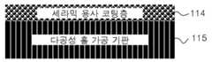
다공성 기판(11)은 도 1과 같이 세라믹 및 그 등가물을 재료로 기공이 존재하는 구조의 단일 기판 일 수도 있고, 도 2 및 도 3과 같이 다양한 기판에 세라믹 용사층을 코팅하는 구조 일 수도 있다.The
도 2는 저기공 또는 무기공 기판(113)에 세라믹 용사 코팅층(114)을 적당한 기공률로 코팅하는 구조 인데, 저기공 또는 무기공 기판(113)은 용사 코팅이 용이한 기판이라면 어떤 것을 사용해도 무관하다.FIG. 2 is a structure in which the ceramic
도 3은 다수의 구멍을 가공을 통해 형성한 다공성 홀 가공 기판(115) 위에 세라믹 용사 코팅층(114)을 적당한 기공률로 코팅한 구조로, 기공률이 없는 기판에 구멍을 뚫어서 식각액 또는 식각가스가 통과 할 수 할 수 있는 통로 역할을 할 수 있게 한다.3 is a structure in which the ceramic thermal
다공성 기판(11)과 세라믹 용사 코팅층(114)은 식각액 또는 식각 가스가 쉽게 통과할 수 있어야 한다.The
다공성 기판(11) 또는 세라믹 용사 코팅층(114)의 기공율은 기공의 밀도와 기공의 크기에 따라 결정되는데, 기공의 밀도는 전체 체적 대비 0.1% 내지 30%의 체적을 차지하는 밀도를 가질 수 있고, 기공의 크기는 1nm내지 10μm 정도로 할 수 있다. 기공의 밀도와 크기는 식각액 또는 식각 가스의 종류에 따라 결정되며, 필요한 식각 속도에 따라 달라질 수 있다. 기공은 식각액 또는 식각 가스가 희생층(12)을 식각할 수 있도록 하는 통로 역할을 한다. 기공율이 대략 0.1%보다 작아지면 식각액 또는 식각 가스가 희생층(12)까지 전달되지 않거나 오랜 시간이 걸리는 문제가 발생 할 수 있고, 기공율이 대략 30%보다 크면 다공성 기판(11)의 기계적 강도 가 너무 약해져서 취급이 어렵고, 희생층의 균일도(uniformity) 저하 문제가 발생 할 수 있다. 또한, 기공의 크기가 대략 1nm보다 작아지면 식각액 또는 식각 가스가 희생층(12)까지 전달되지 않거나 오랜 시간이 걸리는 문제가 발생할 수 있고, 기공의 크기가 대략 10μm보다 크면 다공성 기판(11)의 기계적 강도가 너무 약해져서 취급이 어렵고, 희생층의 균일도(uniformity) 저하 문제가 발생 할 수 있다. 그러나, 상기 다공성 기판(11)중 다공의 기공율, 기공 밀도 및 기공 크기 등을 일정하게 한정하는 것은 아니다.The porosity of the
상기 다공성 기판(11)은 500℃ 이상의 온도에서 물성 변화가 작고, 식각액 또는 식각 가스에 반응이 작아 고온 공정과 리프트 오프 공정이 가능한 특성을 가져야 한다. 즉, 상기 다공성 기판(11) 또는 세라믹 용사 코팅층(114)은 고온에 강해야 하고, 식각액 또는 식각 가스에 사용할 화학 물질에 내식성이 있어야 한다. 일례로 식각액 또는 식각 가스를 불산으로 했을 때는 내식성이 있는 하스테로이(hastelloy) 계열과 같은 금속 재료를 사용할 수 있고, 인산으로 했을 때는 내식성이 있는 금속-STS316(스테인레스), 티타늄(Ti), 하스테로이 계열 중에서 선택된 재료를 사용 할 수 있다. 그러나, 이러한 재질로 본 발명을 한정하는 것은 아니다.The
이와 같이 하여 본 발명은 상기와 같은 다공성 기판(11)을 이용함으로써, 고온의 SPC(Solid Phase Crystallization), MIC(Metal Induced Crystallization), SGS(Super Grain Silicon) 등과 같은 열결정화 방법, 열CVD, PECVD등의 장비를 사용하여 직접 결정화막을 형성하는 방법으로 결정질 실리콘 TFT를 형성하기도 하고, 산화물 반도체 TFT를 제조하는 과정에서 500℃ 이상의 고온에서 열처리 하는 방법 을 포함하여 그 전기적 특성을 높일 수도 있다.In this way, the present invention by using the
다공성 기판(11)의 준비가 완료되면 희생층(12)과 보호막(13)을 차례로 코팅한다.When the preparation of the
희생층(12)은 본 발명의 리프트 오프 공정시 식각액 또는 식각 가스에 의해 제거되어 다공성 기판(11)이 능동형 유기발광소자(22)로부터 쉽게 분리되도록 하는 역할을 한다. 따라서 상기 희생층(12)은 TFT 공정시 고온 공정에서 손상되지 않고, 불산(HF), 인산(H3PO4), 불화암모늄(NH4F), 과산화수소(H2O2), 염산(HCl), 질산(HNO3) 및 황산(H2SO4) 중에서 선택된 어느 하나 또는 그 혼합물과 같은 종류의 식각액 또는 식각 가스와 반응하여 제거되는 재료 이어야 한다. 따라서 상기 희생층(12)은 실리콘 산화막(SiO2), 실리콘 질화막(Si3N4), PSG(phosphor-silicateglass), BPSG(boro-phospho-silicateglass), BSG(boro-silicateglass), 실리콘 카바이드(SiC) 및 그 등가물 중에서 선택된 어느 하나가 증착되어 형성될 수 있다. 또한, 산화 아연(ZnO), ITO(Indium Tin Oxide)와 같은 투명 전극도 희생층으로 사용될 수 있다. 그러나 본 발명에서 상기 희생층(12)의 재질을 한정하는 것은 아니다. 또한 이러한 희생층(12)은 주지된 바와 같이 퍼니스(Furnace), 열CVD(Thermal Chemical Vapor Deposition), LPCVD(Low Pressure CVD), PECVD(Plasma Enhanced Chemical Vapor Deposition) 및 증착기(Evaporator)와 같은 장비중에서 한가지를 선택하여 형성할 수 있다. 희생층(12)은 TFT 제조 공정중 사용되는 가스가 다공성 기판(11)의 기공에 캡쳐되어 있다가 순차적으로 진행되는 다음 공정에 영향을 미치지 않도록 도 4와 같이 다공성 기판(11) 전체를 감싸는 형태로 형성할 수도 있다.The
보호막(13)은 본 발명의 리프트 오프 공정시 식각액 또는 식각 가스로부터 능동형 유기발광소자(22)를 보호하는 역할을 한다. 따라서 상기 보호막(13)은 실리콘 산화막(SiO2), 실리콘 질화막(Si3N4), PSG(phosphor-silicateglass), BPSG(boro-phospho-silicateglass), BSG(boro-silicateglass), 실리콘 카바이드(SiC), 산화 아연(ZnO) 및 ITO(Indium Tin Oxide) 및 그 등가물 중에서 선택된 어느 하나일 수 있으며, 식각액 또는 식각 가스로부터 반응하지 않는 물질이라면 어떤 것을 사용해도 좋다. 이러한 보호막(13)은 역시 퍼니스, 열CVD, LPCVD, PECVD 및 증착기와 같은 장비 중에서 한가지를 선택하여 형성할 수 있다.The
이러한 보호막은 리프트 오프 공정에서 사용되는 식각액 또는 식각가스의 종류에 따라, 또는 유기발광소자의 구조에 따라 생략할 수도 있다.Such a protective film may be omitted depending on the type of etching liquid or etching gas used in the lift-off process or the structure of the organic light emitting device.
두 번째는 도 1의 능동형 유기발광소자(22)의 형성 단계인데, 능동형 유기발광소자(22)는 TFT 파트(part)와 유기발광다이오드 파트로 구분할 수 있다. TFT 파트는 구동회로(14), TFT(15) 및 절연막(16)을 포함한다. 이때, TFT(15)의 형성은 고효율, 고해상도, 대형화의 디스플레이 구현이 가능한 결정질 실리콘 TFT 또는 산화물 반도체 TFT 종류로 하여 고온 공정을 포함하도록 한다. 내열성이 작은 유리 기판이 아닌 다공성 기판(11) 위에 TFT(15)를 형성하기 때문에 고온 공정이 가능하 며, 고온 공정을 적용 함으로써 이동도가 높은 고품질의 TFT(15)를 비교적 저가로 쉽게 형성할 수 있다는 것이 본 발명의 핵심 기술 중 하나이다.Second, the active organic
상기 기술을 적용하여 보다 쉽게 형성할 수 있게 된 결정질 실리콘 TFT는 비정질 실리콘 TFT에 비해 전하이동도가 100배 이상 빠르기 때문에 구동회로(Drive IC)를 따로 장착 하지 않고 패널(Panel) 내에 내장할 수 있다. 구동회로를 내장함으로써 패널의 슬림화, 경량화가 가능하고, 가격을 절감할 수 있으며, 회로 피치의 미세화가 가능하므로 대면적 고해상도 디스플레이를 구현할 수도 있어 응용력과 성능이 탁월한 제품 제작이 가능해진다.The crystalline silicon TFT, which can be formed more easily by applying the above technology, is 100 times faster than the amorphous silicon TFT, and thus can be embedded in a panel without mounting a driver IC. . By incorporating the drive circuit, the panel can be made slimmer, lighter, cost-effective, and the circuit pitch can be made finer, so that a large-area high-resolution display can be realized, resulting in excellent application and performance.
TFT(15)는 어떤 공정 방법을 적용해도 무관하며, 그 구조 역시 제한 없이 적용할 수 있다.The TFT 15 is irrelevant to any process method, and its structure can be applied without limitation.
유기발광다이오드 파트는 제1전극(17), 유기발광부(18), 제2전극(19) 및 실링막(20)으로 구성된다. 제 1 전극(17)과 제 2 전극(19)은 ITO(Indium Tin Oxide), 산화아연(ZnO), 탄소나노튜브(Carbon Nano-Tube)와 같은 투명 전도성 막과, 크롬(Cr), 알루미늄(Al), 몰리브덴(Mo), 은(Ag), 금(Au)등과 같은 불투명 전도성 막을 모두 사용할 수 있다. 이때, 유기발광부(18)의 발광 방식에 따라 제1전극(17)과 제 2 전극(19)에 투명 전도성 막과 불투명 전도성 막을 선택적으로 사용한다. 즉, 배면 발광형(Bottom Emission), 전면 발광형(Top Emission), 양면 발광형(Both top and bottom Emission)으로 나눌 수 있는 발광 방식에 따라 제 1전극(17)과 제 2 전극(19)의 종류를 달리할 수 있다. 실링막(20)은 유기발광부(18)를 수분, 산소, 외부에서 가해질 수 있는 충격으로부터 보호해주는 패키징(Packaging) 역할을 한다. 상부의 실링막(20)은 SiO2, Si3N4, MgF2, In2O3, 고분자 필름, SUS 박막 등이 사용된다.The organic light emitting diode part includes a
세 번째는 기판(21)의 부착 단계이다.The third is the attaching step of the
기판(21)은 능동형 유기발광소자(22)를 형성한 후 도 5및 도6과 같은 리프트 오프 공정이 진행되기에 앞서 기판 접착용 재료를 사용하여 기판을 부착한다. 기판(21)은 유리, PET, 폴리이미드, 플라스틱, 금속등 어떤 재료를 사용해도 무관하다. 본 기판 부착 단계는 실링막(20)이 1mm이상으로 충분히 두꺼운 경우 실시하지 않아도 무관하다.After the active organic
네 번째는 희생층(12)의 제거를 통한 다공성 기판(11)의 분리 단계 이다. 도 5 및 도 6 과 같이 식각액 또는 식각 가스를 다공성 기판(11) 및 세라믹 용사 코팅층(114)의 기공을 통해 통과시키면 희생층(12)이 반응하여 제거된다. 희생층(12)이 식각액 또는 식각 가스에 의해 제거되면 다공성 기판(11)은 자연스럽게 유기발광소자와 분리 된다. 여기서 식각액 또는 식각 가스는 불산(HF), 인산(H3PO4), 불화암모늄(NH4F), 과산화수소(H2O2), 염산(HCl), 질산(HNO3) 및 황산(H2SO4) 중에서 선택된 어느 하나 또는 그 혼합물일 수 있다. 상기 희생층(12)이 질화막 계열일 경우에는 식각액 또는 식각 가스를 인산으로 하고, 산화막 계열일 경우에는 불산을 이용 할 수 있다. 여기서 식각액 또 식각 가스의 종류를 한정하는 것은 아니다. 이와 같은 방법은 리프트 오프 공정으로 고온 공정에 유리한 다공성 기판(11)을 최종 제품인 유기발광소자로부터 분리가 가능하게 한다. 기판(21)은 유리 기판과 같은 투명 기판, 금속 기판과 같은 불투명 기판, PET 기판, 폴리이미드 기판, 플라스틱 기판과 같은 플렉시블 기판 등 다양한 기판을 재료로 할 수 있다. 이와 같이 플렉시블 기판 사용이 용이해 지면서 차세대 디스플레이로 많은 연구가 진행되고 있는 플렉시블 디스플레이 제조를 한층 쉽게 할 수 있다.The fourth step is the separation of the
리프트 오프 유기발광소자를 더욱 얇게, 다양한 모양으로, 쉽게 제조할 수 있게 하는 본 발명의 핵심 기술이다. 또한 리프트 오프 방법은 크게 두 가지가 있는데, 첫째는 도 5와 같이 다공성 기판(11)의 하부에서 식각액 또는 식각 가스를 통과 시켜 희생층을 제거하는 방법이고, 둘째는 도 6과 같이 식각액 또는 식각 가스를 측면에서 통과시켜 희생층을 제거함으로써 세라믹 용사 코팅층(114), 저기공 또는 무기공 기판(113)을 제거하는 방법이다. 그러나 리프트 오프 공정 방법을 이상의 두 가지로 한정하는 것은 아니다.It is a key technology of the present invention to make the lift-off organic light emitting device thinner, in various shapes, and easily manufactured. In addition, there are two methods of lift-off. First, a sacrificial layer is removed by passing an etchant or an etching gas through the lower portion of the
이상에 상세히 기술한 각 단계에 따라 능동형 유기발광소자를 제작하는 방법 이외에도 TFT의 게이트 전극을 리프트 오프 공정 이후에 형성하는 방법도 가능하다.In addition to the method of manufacturing the active organic light emitting device according to each step described in detail above, a method of forming the gate electrode of the TFT after the lift-off process is also possible.
도 7은 도1의 TFT(15)를 상세히 표현한 도면이다.FIG. 7 is a detailed view of the TFT 15 of FIG.
도 7의 구조에서 500℃ 이상의 고온 공정이 적용되는 결정질 실리콘(216)의 형성은 게이트 전극(214)과 절연층(215)이 형성된 이후에 진행하기 때문에 게이트 전극(214)의 내열성이 공정 온도 이하일 경우에는 게이트 전극(214)을 마지막으로 형성해야 한다.In the structure of FIG. 7, since the formation of the
이 공정을 상세히 설명하면 다음과 같다.The process is described in detail as follows.
앞서 기술된 기본 네 단계 공정은 다공성 기판(211)의 준비 및 희생층(212)의 형성, 보호막(213)의 형성 단계, 능동형 유기발광소자(224) 형성 단계, 기판(223)의 부착 단계, 희생층(212)의 제거를 통한 다공성 기판(211)의 분리 단계로 구분할 수 있다. 이 같은 기본 공정 단계 중, 능동형 유기발광소자(224)의 형성 단계에서 게이트 전극(214)을 제외한 나머지를 모두 형성한 후 다공성 기판(211)의 분리 단계를 진행하고 보호막(213)을 제거한 후 절연막(215)를 패터닝하여 적정 위치(예를 들면, 결정질 실리콘과 대응되는 위치)에 게이트 전극(214)을 형성한다. 이때 절연막(215)이 보호막(213)을 대신할 수도 있으며, 절연막(215)의 두께를 조절하여 적용할 수도 있다. 도 7에서 미설명 부호 216은 게이트 전극(214) 및 절연막(215) 위에 형성된 결정질 실리콘이고, 217은 결정질 실리콘중 N+층이며, 218은 소스 전극 및 드레인 전극을 의미한다. 물론, 소스 전극 및 드레인 전극은 서로 이격되어 형성되며, 드레인 전극이 제1전극(219)에 전기적으로 연결된다.The basic four-step process described above includes preparing the
이상에서 설명한 내용은 본 발명에 의한 능동형 유기발광소자를 제조하는 하나의 실시예에 불과하다. 본 발명은 상기한 실시예에 한정되지 않고, 발명의 요지에서 벗어나지 않는 한도 내에서 다양하게 변경하여 실시 할 수 있다.The above description is just one embodiment of manufacturing an active organic light emitting diode according to the present invention. The present invention is not limited to the above-described embodiments, and various modifications can be made without departing from the spirit of the invention.
도 1은 본 발명의 일실시 예로 일반적인 능동형 유기발광소자를 포함하는 구조를 나타낸 도면이다.1 is a view showing a structure including a general active organic light emitting device according to an embodiment of the present invention.
도 2는 본 발명의 다공성 기판의 구조 중 세라믹 용사 코팅한 형태를 나타내는 도면이다.2 is a view showing a ceramic thermal spray coating of the structure of the porous substrate of the present invention.
도 3는 본 발명의 다공성 기판의 구조 중 하나로 가공을 통해 다공성 홀을 형성한 후 세라믹을 용사 코팅하는 구조를 나타내는 도면이다.Figure 3 is a view showing the structure of the thermal spray coating the ceramic after forming a porous hole through the processing of one of the structure of the porous substrate of the present invention.
도 4는 본 발명의 희생층 형성 방법 중 다공성 기판을 전부 감싸는 형태를 나타내는 도면이다.4 is a view showing a form surrounding the entire porous substrate of the sacrificial layer forming method of the present invention.
도 5는 본 발명의 리프트 오프 공정 방법 중 하나를 나타내는 도면이다.5 is a view showing one of the lift off process method of the present invention.
도 6은 본 발명의 리프트 오프 공정 방법 중 다른 하나를 나타내는 도면이다.6 is a view showing another one of the lift off process method of the present invention.
도 7은 본 발명의 도 1을 상세히 표현한 구조를 나타내는 도면이다.FIG. 7 is a view showing the structure of FIG. 1 of the present invention in detail.
Claims (22)
Translated fromKoreanPriority Applications (1)
| Application Number | Priority Date | Filing Date | Title |
|---|---|---|---|
| PCT/KR2009/007416WO2010131827A1 (en) | 2009-05-13 | 2009-12-11 | Organic light emitting diodes using porous substrates and manufacturing method thereof |
Applications Claiming Priority (2)
| Application Number | Priority Date | Filing Date | Title |
|---|---|---|---|
| KR20090041765 | 2009-05-13 | ||
| KR1020090041765 | 2009-05-13 |
Publications (2)
| Publication Number | Publication Date |
|---|---|
| KR20100122842A KR20100122842A (en) | 2010-11-23 |
| KR101157659B1true KR101157659B1 (en) | 2012-06-18 |
Family
ID=43407673
Family Applications (1)
| Application Number | Title | Priority Date | Filing Date |
|---|---|---|---|
| KR1020090092528AExpired - Fee RelatedKR101157659B1 (en) | 2009-05-13 | 2009-09-29 | Manufacture Method of Organic Light Emitting Diodes Using Porous Substrate |
Country Status (1)
| Country | Link |
|---|---|
| KR (1) | KR101157659B1 (en) |
Cited By (1)
| Publication number | Priority date | Publication date | Assignee | Title |
|---|---|---|---|---|
| KR20150113482A (en)* | 2014-03-31 | 2015-10-08 | 동우 화인켐 주식회사 | Manufacturing method of an array substrate for liquid crystal display |
Families Citing this family (3)
| Publication number | Priority date | Publication date | Assignee | Title |
|---|---|---|---|---|
| CN102255055B (en)* | 2011-06-29 | 2013-02-20 | 彩虹(佛山)平板显示有限公司 | Method for reducing nitrogen consumption in OLED (Organic Light Emitting Diode) production process |
| KR102215812B1 (en) | 2014-01-09 | 2021-02-17 | 삼성디스플레이 주식회사 | Manufacturing method of device substrate and display device manufatured by using the method |
| KR102324765B1 (en) | 2015-02-09 | 2021-11-10 | 삼성디스플레이 주식회사 | Organic light emitting diode display and method of manufacturing the same |
Citations (4)
| Publication number | Priority date | Publication date | Assignee | Title |
|---|---|---|---|---|
| KR20030007208A (en)* | 2001-07-16 | 2003-01-23 | 가부시키가이샤 한도오따이 에네루기 켄큐쇼 | Semiconductor device and peeling off method and method of manufacturing semiconductor device |
| KR20040053495A (en)* | 2002-12-14 | 2004-06-24 | 삼성에스디아이 주식회사 | Method for making substrate and method for making Organic electro luminescence display device using the same,Organic electro luminescence display device |
| KR20050084104A (en)* | 2002-12-03 | 2005-08-26 | 코닌클리즈케 필립스 일렉트로닉스 엔.브이. | Method for the manufacture of a display |
| KR20080004067A (en)* | 2006-07-04 | 2008-01-09 | 삼성에스디아이 주식회사 | Manufacturing Method of Flat Panel Display |
- 2009
- 2009-09-29KRKR1020090092528Apatent/KR101157659B1/ennot_activeExpired - Fee Related
Patent Citations (4)
| Publication number | Priority date | Publication date | Assignee | Title |
|---|---|---|---|---|
| KR20030007208A (en)* | 2001-07-16 | 2003-01-23 | 가부시키가이샤 한도오따이 에네루기 켄큐쇼 | Semiconductor device and peeling off method and method of manufacturing semiconductor device |
| KR20050084104A (en)* | 2002-12-03 | 2005-08-26 | 코닌클리즈케 필립스 일렉트로닉스 엔.브이. | Method for the manufacture of a display |
| KR20040053495A (en)* | 2002-12-14 | 2004-06-24 | 삼성에스디아이 주식회사 | Method for making substrate and method for making Organic electro luminescence display device using the same,Organic electro luminescence display device |
| KR20080004067A (en)* | 2006-07-04 | 2008-01-09 | 삼성에스디아이 주식회사 | Manufacturing Method of Flat Panel Display |
Cited By (2)
| Publication number | Priority date | Publication date | Assignee | Title |
|---|---|---|---|---|
| KR20150113482A (en)* | 2014-03-31 | 2015-10-08 | 동우 화인켐 주식회사 | Manufacturing method of an array substrate for liquid crystal display |
| KR102092351B1 (en) | 2014-03-31 | 2020-03-23 | 동우 화인켐 주식회사 | Manufacturing method of an array substrate for liquid crystal display |
Also Published As
| Publication number | Publication date |
|---|---|
| KR20100122842A (en) | 2010-11-23 |
Similar Documents
| Publication | Publication Date | Title |
|---|---|---|
| TWI592072B (en) | Flexible display apparatus | |
| US9166191B2 (en) | Display device, method of manufacturing the display device and carrier substrate for manufacturing display device | |
| US9799682B2 (en) | Method for manufacturing semiconductor device | |
| US9355877B2 (en) | Carrier substrate, method of manufacturing the same, and method of manufacturing flexible display device using the carrier substrate | |
| CN101626035B (en) | Poly silicon thin film transistor and method of fabricating the same | |
| CN104538429B (en) | Manufacturing method and structure of AMOLED backplane | |
| CN107302012B (en) | Flexible OLED array substrate, manufacturing method thereof and OLED display panel | |
| US20170117498A1 (en) | Thin-film device and manufacturing method thereof | |
| US9385174B2 (en) | Organic light-emitting diode display and manufacturing method thereof | |
| WO2018232949A1 (en) | OLED panel packaging method | |
| US9136353B2 (en) | Polysilicon-based thin film transistor | |
| US9184224B2 (en) | Organic light-emitting diode display and manufacturing method thereof | |
| KR101157659B1 (en) | Manufacture Method of Organic Light Emitting Diodes Using Porous Substrate | |
| CN102751200B (en) | Thin film transistor, array substrateand manufacturing method thereof | |
| WO2021259361A1 (en) | Thin-film transistor and manufacturing method therefor, and array substrate and display panel | |
| CN106067443A (en) | Display device and method of manufacturing same | |
| WO2016176879A1 (en) | Method for fabricating amoled back plate, and structure thereof | |
| US20210091120A1 (en) | Tft array substrate and manufacturing method thereof | |
| WO2010131827A1 (en) | Organic light emitting diodes using porous substrates and manufacturing method thereof | |
| WO2019153430A1 (en) | Tft substrate and manufacturing method therefor, and oled substrate | |
| KR20100010978A (en) | Display substrate and method of manufacturing the same | |
| KR20080000299A (en) | Polysilicon Thin Film Transistor Liquid Crystal Display and Manufacturing Method Thereof | |
| JP2007123698A (en) | Thin film transistor and manufacturing method thereof | |
| JP2016213380A (en) | Thin film device and manufacturing method thereof | |
| Jang et al. | 77.1: Invited paper: TFT technologies for flexible displays |
Legal Events
| Date | Code | Title | Description |
|---|---|---|---|
| A201 | Request for examination | ||
| PA0109 | Patent application | St.27 status event code:A-0-1-A10-A12-nap-PA0109 | |
| PA0201 | Request for examination | St.27 status event code:A-1-2-D10-D11-exm-PA0201 | |
| PG1501 | Laying open of application | St.27 status event code:A-1-1-Q10-Q12-nap-PG1501 | |
| D13-X000 | Search requested | St.27 status event code:A-1-2-D10-D13-srh-X000 | |
| D14-X000 | Search report completed | St.27 status event code:A-1-2-D10-D14-srh-X000 | |
| E902 | Notification of reason for refusal | ||
| PE0902 | Notice of grounds for rejection | St.27 status event code:A-1-2-D10-D21-exm-PE0902 | |
| E13-X000 | Pre-grant limitation requested | St.27 status event code:A-2-3-E10-E13-lim-X000 | |
| P11-X000 | Amendment of application requested | St.27 status event code:A-2-2-P10-P11-nap-X000 | |
| P13-X000 | Application amended | St.27 status event code:A-2-2-P10-P13-nap-X000 | |
| R17-X000 | Change to representative recorded | St.27 status event code:A-3-3-R10-R17-oth-X000 | |
| R17-X000 | Change to representative recorded | St.27 status event code:A-3-3-R10-R17-oth-X000 | |
| PE0902 | Notice of grounds for rejection | St.27 status event code:A-1-2-D10-D21-exm-PE0902 | |
| E13-X000 | Pre-grant limitation requested | St.27 status event code:A-2-3-E10-E13-lim-X000 | |
| P11-X000 | Amendment of application requested | St.27 status event code:A-2-2-P10-P11-nap-X000 | |
| P13-X000 | Application amended | St.27 status event code:A-2-2-P10-P13-nap-X000 | |
| E701 | Decision to grant or registration of patent right | ||
| PE0701 | Decision of registration | St.27 status event code:A-1-2-D10-D22-exm-PE0701 | |
| GRNT | Written decision to grant | ||
| PR0701 | Registration of establishment | St.27 status event code:A-2-4-F10-F11-exm-PR0701 | |
| PR1002 | Payment of registration fee | St.27 status event code:A-2-2-U10-U11-oth-PR1002 Fee payment year number:1 | |
| PG1601 | Publication of registration | St.27 status event code:A-4-4-Q10-Q13-nap-PG1601 | |
| R18-X000 | Changes to party contact information recorded | St.27 status event code:A-5-5-R10-R18-oth-X000 | |
| PR1001 | Payment of annual fee | St.27 status event code:A-4-4-U10-U11-oth-PR1001 Fee payment year number:4 | |
| FPAY | Annual fee payment | Payment date:20160311 Year of fee payment:5 | |
| PR1001 | Payment of annual fee | St.27 status event code:A-4-4-U10-U11-oth-PR1001 Fee payment year number:5 | |
| FPAY | Annual fee payment | Payment date:20170316 Year of fee payment:6 | |
| PR1001 | Payment of annual fee | St.27 status event code:A-4-4-U10-U11-oth-PR1001 Fee payment year number:6 | |
| PN2301 | Change of applicant | St.27 status event code:A-5-5-R10-R13-asn-PN2301 St.27 status event code:A-5-5-R10-R11-asn-PN2301 | |
| FPAY | Annual fee payment | Payment date:20180327 Year of fee payment:7 | |
| PR1001 | Payment of annual fee | St.27 status event code:A-4-4-U10-U11-oth-PR1001 Fee payment year number:7 | |
| PC1903 | Unpaid annual fee | St.27 status event code:A-4-4-U10-U13-oth-PC1903 Not in force date:20190613 Payment event data comment text:Termination Category : DEFAULT_OF_REGISTRATION_FEE | |
| PC1903 | Unpaid annual fee | St.27 status event code:N-4-6-H10-H13-oth-PC1903 Ip right cessation event data comment text:Termination Category : DEFAULT_OF_REGISTRATION_FEE Not in force date:20190613 | |
| P22-X000 | Classification modified | St.27 status event code:A-4-4-P10-P22-nap-X000 | |
| P22-X000 | Classification modified | St.27 status event code:A-4-4-P10-P22-nap-X000 |