KR101156060B1 - Method for fabricating semiconductor device with buried gate - Google Patents
Method for fabricating semiconductor device with buried gateDownload PDFInfo
- Publication number
- KR101156060B1 KR101156060B1KR1020100128116AKR20100128116AKR101156060B1KR 101156060 B1KR101156060 B1KR 101156060B1KR 1020100128116 AKR1020100128116 AKR 1020100128116AKR 20100128116 AKR20100128116 AKR 20100128116AKR 101156060 B1KR101156060 B1KR 101156060B1
- Authority
- KR
- South Korea
- Prior art keywords
- forming
- substrate
- storage node
- gate
- region
- Prior art date
- Legal status (The legal status is an assumption and is not a legal conclusion. Google has not performed a legal analysis and makes no representation as to the accuracy of the status listed.)
- Expired - Fee Related
Links
Images


Classifications
- H—ELECTRICITY
- H10—SEMICONDUCTOR DEVICES; ELECTRIC SOLID-STATE DEVICES NOT OTHERWISE PROVIDED FOR
- H10D—INORGANIC ELECTRIC SEMICONDUCTOR DEVICES
- H10D64/00—Electrodes of devices having potential barriers
- H10D64/20—Electrodes characterised by their shapes, relative sizes or dispositions
- H10D64/27—Electrodes not carrying the current to be rectified, amplified, oscillated or switched, e.g. gates
- H10D64/311—Gate electrodes for field-effect devices
- H10D64/411—Gate electrodes for field-effect devices for FETs
- H10D64/511—Gate electrodes for field-effect devices for FETs for IGFETs
- H10D64/512—Disposition of the gate electrodes, e.g. buried gates
- H10D64/513—Disposition of the gate electrodes, e.g. buried gates within recesses in the substrate, e.g. trench gates, groove gates or buried gates
- H—ELECTRICITY
- H10—SEMICONDUCTOR DEVICES; ELECTRIC SOLID-STATE DEVICES NOT OTHERWISE PROVIDED FOR
- H10B—ELECTRONIC MEMORY DEVICES
- H10B12/00—Dynamic random access memory [DRAM] devices
- H10B12/01—Manufacture or treatment
- H10B12/02—Manufacture or treatment for one transistor one-capacitor [1T-1C] memory cells
- H10B12/05—Making the transistor
- H10B12/053—Making the transistor the transistor being at least partially in a trench in the substrate
- H—ELECTRICITY
- H10—SEMICONDUCTOR DEVICES; ELECTRIC SOLID-STATE DEVICES NOT OTHERWISE PROVIDED FOR
- H10B—ELECTRONIC MEMORY DEVICES
- H10B12/00—Dynamic random access memory [DRAM] devices
- H10B12/01—Manufacture or treatment
- H10B12/09—Manufacture or treatment with simultaneous manufacture of the peripheral circuit region and memory cells
- H—ELECTRICITY
- H10—SEMICONDUCTOR DEVICES; ELECTRIC SOLID-STATE DEVICES NOT OTHERWISE PROVIDED FOR
- H10B—ELECTRONIC MEMORY DEVICES
- H10B12/00—Dynamic random access memory [DRAM] devices
- H10B12/30—DRAM devices comprising one-transistor - one-capacitor [1T-1C] memory cells
- H10B12/48—Data lines or contacts therefor
- H10B12/482—Bit lines
Landscapes
- Engineering & Computer Science (AREA)
- Manufacturing & Machinery (AREA)
- Semiconductor Memories (AREA)
- Internal Circuitry In Semiconductor Integrated Circuit Devices (AREA)
Abstract
Description
Translated fromKorean본 발명은 반도체 장치의 제조 기술에 관한 것으로, 특히 매립게이트(Buried Gate, BG)를 구비한 반도체 장치 제조방법에 관한 것이다.
BACKGROUND OF THE INVENTION 1. Field of the Invention The present invention relates to a manufacturing technique of a semiconductor device, and more particularly to a method of manufacturing a semiconductor device having a buried gate (BG).
현재 반도체 제조공정에서 미세화가 진행됨에 따른 여러가지 소자특성과 공정 구현이 힘들어 지고 있다. 특히 40nm 이하로 갈수록 게이트 구조, 비트라인 구조, 콘택 구조 등의 형성이 한계를 보이고 있고, 가령 구조가 형성된다 하더라도 원하는 소자특성을 확보하는데 어려움이 있다. 이에 따라 최근에는 게이트를 기판에 매립하여 형성하는 매립게이트(Buried Gate, BG)가 도입되었다.As the miniaturization progresses in the semiconductor manufacturing process, various device characteristics and processes are becoming difficult. In particular, the formation of the gate structure, the bit line structure, the contact structure, and the like shows a limit toward 40 nm or less, and even if the structure is formed, it is difficult to secure desired device characteristics. Accordingly, recently, buried gates (BGs), which are formed by embedding a gate in a substrate, have been introduced.
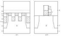
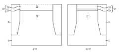
도 1a 내지 도 1c는 종래기술에 따른 매립게이트를 구비한 반도체 장치 제조방법을 도시한 공정단면도이다.1A to 1C are cross-sectional views illustrating a method of manufacturing a semiconductor device having a buried gate according to the related art.
도 1a에 도시된 바와 같이, 셀영역과 페리영역을 갖는 기판(11)에 활성영역(13)을 정의하는 소자분리막(12)을 형성한 다음, 셀영역의 기판(11) 상에 랜딩플러그(14)를 형성하고, 기판(11)에는 매립게이트를 형성한다. 매립게이트는 기판에 형성된 트렌치(15), 트렌치(15) 표면상에 형성된 게이트절연막(미도시), 트렌치를 일부 매립하는 게이트전극(16) 및 나머지 트렌치(15)를 매립하는 게이트하드마스크막(17)을 포함한다. 이어서, 기판(11) 상에 셀영역을 덮고, 페리영역을 오픈하는 캡핑막(18)을 형성한 다음, 캡핑막(18)을 이용하여 페리영역의 기판(11)을 노출시킨다.As shown in FIG. 1A, an
도 1b에 도시된 바와 같이, 페리영역에 페리게이트절연막(19), 페리게이트전극(20) 및 페리게이트하드마스크막(21)이 순차적으로 적층된 구조의 페리게이트(22)를 형성한다. 이어서, 페리게이트(22) 측벽에 스페이서(23)를 형성하고, 셀영역을 캡핑막(18)을 제거한다. 이어서, 기판(11) 전면에 페리게이트(22)를 덮는 층간절연막(24)을 형성한다.As shown in FIG. 1B, a
도 1c에 도시된 바와 같이, 셀영역에 층간절연막(24)을 관통하여 랜딩플러그(14)에 접하는 스토리지노드콘택플러그(26) 및 층간절연막(24)에 형성된 다마신패턴(27)을 일부 매립하는 비트라인(29)을 형성한다. 여기서, 미설명 도면부호 '25'는 스토리지노드콘택홀, '28'은 비트라인스페이서, '30'은 비트라인하드마스크막이다.As shown in FIG. 1C, the storage
하지만, 종래기술에 따른 반도체 장치 제조방법은 페리게이트(22)를 형성한 이후에 스토리지노드콘택플러그(26) 및 비트라인(29)을 형성하기 때문에 이들 형성공정에 대한 공정마진이 저하되는 문제점이 있다. 이는 페리게이트(22) 형성공정과 스토리지노드콘택플러그(26) 형성공정 및 비트라인(29) 형성공정 사이에 진행되는 공정들에서 발생하는 공정 산포를 모두 포함한 상태에서 스토리지노드콘택플러그(26) 형성공정 및 비트라인(29) 형성공정이 진행되기 때문이다. 상술한 스토리지노드콘택플러그(26) 형성공정에 대한 공정마진 저하는 스토리지노드콘택플러그(26)의 콘택특성을 저하시키고, 높이 산포를 유발하여 후속 스토리지노드 형성공정에 대한 난이도를 증가시키는 문제점이 있다. 그리고, 비트라인(29) 형성공정에 대한 공정마진 저하는 비트라인(29)의 콘택특성을 저하시키고, 높이 산포를 유발하여 비트라인(29)의 저항을 증가시키거나, 비트라인(29) 저항 산포를 유발하는 문제점이 있다.
However, since the semiconductor device manufacturing method according to the related art forms the storage
본 발명은 상기한 종래기술의 문제점을 해결하기 위하여 제안된 것으로, 스토리지노드콘택플러그 형성공정 및 비트라인 형성공정에 대한 공정마진을 향상시킬 수 있는 매립게이트를 구비한 반도체 장치 제조방법을 제공하는데 그 목적이 있다.
The present invention has been proposed to solve the above problems of the prior art, and provides a semiconductor device manufacturing method having a buried gate that can improve the process margin for the storage node contact plug forming process and the bit line forming process. There is a purpose.
상기 목적을 달성하기 위한 일 측면에 따른 본 발명은 셀영역과 페리영역을 갖는 기판의 상기 셀영역의 기판에 매립게이트를 형성하는 단계; 상기 기판상에 제1층간절연막을 형성하는 단계; 상기 셀영역의 제1층간절연막을 선택적으로 식각하여 다마신패턴을 형성하는 단계; 상기 다마신패턴 내부에 비트라인을 형성하는 단계; 및 상기 페리영역에 페리게이트를 형성하는 단계를 포함하는 반도체 장치 제조방법을 제공한다.According to an aspect of the present invention, there is provided a method including: forming a buried gate in a substrate of a cell region of a substrate having a cell region and a ferry region; Forming a first interlayer insulating film on the substrate; Selectively etching the first interlayer dielectric layer of the cell region to form a damascene pattern; Forming a bit line in the damascene pattern; And forming a ferrite in the ferry region.
또한, 본 발명의 반도체 장치 제조방법은 상기 다마신패턴을 형성하기 이전에, 상기 제1층간절연막을 선택적으로 식각하여 스토리지노드콘택홀을 형성하는 단계; 및 상기 스토리지노드콘택홀을 매립하는 스토리지노드콘택플러그를 형성하는 단계를 더 포함할 수 있다.
The method of manufacturing a semiconductor device of the present invention may further include forming a storage node contact hole by selectively etching the first interlayer insulating layer before the damascene pattern is formed; And forming a storage node contact plug to fill the storage node contact hole.
상기 목적을 달성하기 위한 다른 일 측면에 따른 본 발명은 셀영역과 페리영역을 갖는 기판의 상기 셀영역에 랜딩플러그를 형성함과 동시에 매립게이트를 형성하는 단계; 상기 기판상에 제1층간절연막을 형성하는 단계; 상기 셀영역의 제1층간절연막을 선택적으로 식각하여 상기 랜딩플러그를 노출시키는 다마신패턴을 형성하는 단계; 상기 다마신패턴 아래 랜딩플러그를 제거하는 단계; 상기 랜딩플러그가 제거된 영역 및 상기 다마신패턴 내부에 비트라인을 형성하는 단계; 및 상기 페리영역에 페리게이트를 형성하는 단계를 포함하는 반도체 장치 제조방법을 제공한다.According to another aspect of the present invention, there is provided a method of forming a buried gate while simultaneously forming a landing plug in the cell region of a substrate having a cell region and a ferry region; Forming a first interlayer insulating film on the substrate; Selectively etching the first interlayer dielectric layer of the cell region to form a damascene pattern exposing the landing plug; Removing a landing plug under the damascene pattern; Forming a bit line in the region where the landing plug is removed and in the damascene pattern; And forming a ferrite in the ferry region.
또한, 본 발명의 반도체 장치 제조방법은 상기 다마신패턴을 형성하기 이전에, 상기 제1층간절연막을 선택적으로 식각하여 스토리지노드콘택홀을 형성하는 단계; 및 상기 스토리지노드콘택홀을 매립하는 스토리지노드콘택플러그를 형성하는 단계를 더 포함할 수 있다.
The method of manufacturing a semiconductor device of the present invention may further include forming a storage node contact hole by selectively etching the first interlayer insulating layer before the damascene pattern is formed; And forming a storage node contact plug to fill the storage node contact hole.
상술한 과제 해결 수단을 바탕으로 하는 본 발명은 페리게이트를 형성하기 이전에 셀영역에 스토리지노드콘택플러그 및 비트라인을 형성함으로써, 공정 산포에 기인한 스토리지노드콘택플러그 형성공정 및 비트라인 형성공정에 대한 공정마진 저하를 방지할 수 있는 효과가 있다.
The present invention, based on the above-mentioned problem solving means, forms the storage node contact plug and the bit line in the cell region before forming the ferrite, thereby forming the storage node contact plug forming process and the bit line forming process due to process dispersion. There is an effect that can prevent a decrease in process margin.
도 1a 내지 도 1c는 종래기술에 따른 매립게이트를 구비한 반도체 장치 제조방법을 도시한 공정단면도.
도 2a 내지 도 2h는 본 발명의 일실시예에 따른 매립게이트를 구비한 반도체 장치 제조방법을 도시한 공정단면도.1A to 1C are cross-sectional views illustrating a method of manufacturing a semiconductor device having a buried gate according to the prior art.
2A to 2H are cross-sectional views illustrating a method of manufacturing a semiconductor device having a buried gate according to an embodiment of the present invention.
이하 본 발명이 속하는 기술분야에서 통상의 지식을 가진자가 본 발명의 기술적 사상을 용이하게 실시할 수 있을 정도로 상세히 설명하기 위하여, 본 발명의 가장 바람직한 실시예를 첨부도면을 참조하여 설명하기로 한다. 후술할 본 발명은 매립게이트를 구비한 반도체 장치에서 스토리지노드콘택플러그 형성공정 및 비트라인 형성공정에 대한 공정마진을 향상시킬 수 있는 반도체 장치 제조방법을 제공한다. 이를 위해, 본 발명은 셀영역에 스토리지노드콘택플러그 및 비트라인을 형성한 다음에 페리영역에 페리게이트를 형성하는 것을 특징으로 한다.
DETAILED DESCRIPTION OF THE PREFERRED EMBODIMENT Hereinafter, preferred embodiments of the present invention will be described in detail with reference to the accompanying drawings, in order to facilitate a person skilled in the art to easily carry out the technical idea of the present invention. The present invention to be described later provides a method of manufacturing a semiconductor device capable of improving process margins for a storage node contact plug forming process and a bit line forming process in a semiconductor device having a buried gate. To this end, the present invention is characterized by forming a storage node contact plug and a bit line in the cell region and then forming a ferrite in the ferry region.
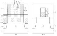
도 2a 내지 도 2h는 본 발명의 일실시예에 따른 매립게이트를 구비한 반도체 장치 제조방법을 도시한 공정단면도이다.2A to 2H are cross-sectional views illustrating a method of manufacturing a semiconductor device having a buried gate according to an embodiment of the present invention.
도 2a에 도시된 바와 같이, 셀영역과 페리영역을 갖는 기판(31) 상에 패드산화막(32A)과 하드마스크폴리실리콘막(32B)이 순차적으로 적층된 제1하드마스크패턴(32)을 형성한다. 제1하드마스크패턴(32)은 후속 공정을 통해 형성될 랜딩플러그의 높이를 고려하여 600Å 내지 1500Å 범위의 두께를 갖도록 형성할 수 있다.As shown in FIG. 2A, a first
다음으로, 제1하드마스크패턴(32)을 식각장벽으로 기판(31)을 식각하여 소자분리트렌치를 형성하고, 소자분리트렌치를 절연물질로 매립하여 활성영역(34)을 정의하는 소자분리막(33)을 형성한다.Subsequently, the
다음으로, 셀영역의 제1하드마스크패턴(32)을 선택적으로 제거하여 활성영역(34)을 노출시키는 홈(35)을 형성한다.Next, the first
도 2b에 도시된 바와 같이, 홈(35)을 매립하도록 기판(31) 전면에 랜딩플러그용 도전막(36)을 형성한 후에, 소자분리막(33)이 노출될때까지 평탄화공정을 실시한다. 이때, 랜딩플러그용 도전막(36)은 폴리실리콘막으로 형성할 수 있고, 평탄화공정을 화학적기계적연마법(CMP)을 사용하여 실시할 수 있다.As shown in FIG. 2B, after the conductive plug 36 for the landing plug is formed on the entire surface of the
다음으로, 셀영역에 매립게이트를 형성하기 위하여 랜딩플러그용 도전막(36)이 형성된 기판(31) 상에 제2하드마스크패턴(37)을 형성한다. 일례로, 제2하드마스크패턴(37)은 질화막으로 형성할 수 있다.Next, a second
도 2c에 도시된 바와 같이, 제2하드마스크패턴(37)을 식각장벽으로 랜딩플러그용 도전막(36), 활성영역(34) 및 소자분리막(33)을 식각한다. 이로써, 활성영역(34)과 소자분리막(33)을 동시에 가로지르는 다수의 트렌치(38)가 형성됨과 동시에 랜딩플러그(36A)가 형성된다.As illustrated in FIG. 2C, the landing plug conductive layer 36, the
다음으로, 트렌치(38) 표면상에 게이트절연막(미도시)을 형성한다. 일례로, 게이트절연막은 열산화법(ThermalOxidation)을 사용하여 실리콘산화막(SiO2)으로 형성할 수 있다.Next, a gate insulating film (not shown) is formed on the
다음으로, 트렌치(38)를 일부 매립하는 게이트전극(39)을 형성한다. 게이트전극(39)은 금속막, 금속산화막, 금속질화막, 금속실리사이드막을 포함하는 금속성막으로 형성할 수 있다.Next, a
다음으로, 게이트전극(39) 상에 나머지 트렌치(38)를 매립하는 실링막(40)을 형성한다. 일례로, 실링막(40)은 질화막으로 형성할 수 있다.Next, a
상술한 공정과정을 통해 셀영역의 기판(31)에 다수의 매립게이트를 형성할 수 있으며, 매립게이트 형성공정간 페리영역 형성된 제2하드마스크패턴(37)에 의하여 페리영역의 기판(31)이 손실(또는 손상)되는 것을 방지할 수 있다.Through the above-described process, a plurality of buried gates may be formed on the
도 2d에 도시된 바와 같이, 기판(31) 전면에 식각정지막(41) 및 제1층간절연막(42)을 순차적으로 형성한다. 식각정지막(41)과 제1층간절연막(42)은 서로 식각선택비를 갖는 물질로 형성하는 것이 바람직하다. 일례로, 식각정지막(41)은 질화막으로 형성할 수 있고, 제1층간절연막(42)은 산화막으로 형성할 수 있다.As shown in FIG. 2D, an
다음으로, 스토리지노드콘택플러그 예정지역의 제1층간절연막(42), 식각방지막(41) 및 제2하드마스크패턴(37)을 선택적으로 식각하여 랜딩플러그(36A)를 노출시키는 스토리지노드콘택홀(43)을 형성한다. 이때, 스토리지노드콘택홀(43)은 각각의 스토리지노드콘택플러그 예정지역을 오픈하는 홀타입(Hole type), 인접한 스토리지노드콘택플러그 예정지역을 동시에 오픈하는 바타입(Bar type) 및 매립게이트와 평행한 방향으로 연장되어 동일 선상에 위치하는 스토리지노드콘택플러그 예정지역을 모두 오픈하는 라인타입(Line type)으로 이루어진 그룹으로부터 선택된 어느 하나의 타입으로 형성할 수 있다.Next, the storage node contact hole exposing the
다음으로, 스토리지노드콘택홀(43)을 도전물질로 매립하여 스토리지노드콘택플러그(44)를 형성한다.Next, the storage
여기서, 본 발명은 페리영역에 페리게이트를 형성하기 이전에 제1층간절연막(42)을 형성하고, 스토리지노드콘택홀(43) 및 스토리지노드콘택플러그(44)를 형성하기 때문에 기존의 공정 산포에 의하여 스토리지노드콘택플러그(44) 형성공정에 대한 공정마진이 저하되는 것을 방지할 수 있다.Here, the present invention forms the first
도 2e에 도시된 바와 같이, 제1층간절연막(42), 식각정지막(41) 및 제2하드마스크패턴(37)을 선택적으로 식각하여 랜딩플러그(36A)를 노출시키는 다마신패턴(45)을 형성한다. 이때, 다마신패턴(45)은 매립게이트와 교차하는 방향으로 연장된 라인패턴으로 형성할 수 있다.As shown in FIG. 2E, the
다음으로, 다마신패턴(45) 아래 랜딩플러그(36A)를 제거한다. 이때, 다마신패턴(45) 아래 랜딩플러그(36A)를 제거하는 이유는 기형성된 스토리지노드콘택플러그(44)와 다마신패턴(45) 내부에 형성될 비트라인 사이의 쇼트를 방지함과 동시에 후속 페리게이트 형성공정에 대한 공정마진을 향상시키기 위함이다. 다마신패턴(45) 아래 랜딩플러그(36A)는 도면에 도시된 바와 같이, 모두 제거하거나, 또는 일부만 제거할 수 있다.Next, the
참고로, 스토리지노드콘택홀(43)을 바타입 또는 라인타입으로 형성한 경우에는 다마신패턴(45) 형성공정시 제1층간절연막(42)과 더불어서 스토리지노드콘택플러그(44)를 식각하여 인접한 스토리지노드콘택플러그(44) 사이를 전기적으로 분리시킨다. 따라서, 스토리지노드콘택홀(43)을 바타입 또는 라인타입으로 형성한 경우에는 다마신패턴(45) 형성공정이 완료된 시점에서 실질적으로 스토리지노드콘택플러그(44)가 형성된다.For reference, when the storage
도 2f에 도시된 바와 같이, 다마신패턴(45) 측벽에 비트라인스페이서(46)를 형성한다. 비트라인스페이서(46)는 산화막, 질화막 및 산화질화막으로 이루어진 그룹으로부터 선택된 어느 하나의 단일막으로 형성하거나, 또는 이들이 적층된 적층막으로 형성할 수 있다.As shown in FIG. 2F, the
다음으로, 다마신패턴(45) 아래 랜딩플러그(36A)가 제거된 공간 및 다마신패턴(45)을 일부 매립하는 비트라인(47)을 형성한다. 비트라인(47)은 기판(31)과 접하며, 금속성막으로 형성할 수 있다. 비트라인(47)은 다마신패턴(45)을 매립하도록 금속성막을 증착한 다음, 전면식각공정 예컨대, 에치백을 실시하는 일련의 공정과정을 통해 형성할 수 있다.Next, a space in which the
한편, 비트라인(47)과 기판(31) 사이의 콘택저항을 감소시키기 위하여 이들 사이에 오믹콘택층(미도시)을 형성할 수도 있다. 이때, 오믹콘택층은 금속실리사이드로 형성할 수 있다. 일례로, 다마신패턴(45) 형성공정시 랜딩플러그(36A)를 일부만 제거한 경우에는 잔류하는 랜딩플러그와 금속을 반응시켜 오믹콘택층을 형성할 수 있다. 또한, 랜딩플러그(36A)를 완전히 제거한 경우에도 기판(31)과 금속을 반응시켜 오믹콘택층을 형성할 수 있다.On the other hand, in order to reduce the contact resistance between the
다음으로, 비트라인(47) 상에 나머지 다마신패턴(45)을 매립하는 비트라인하드마스크막(48)을 형성한다. 비트라인하드마스크막(48)은 산화막, 질화막 및 산화질화막으로 이루어진 그룹으로부터 선택된 어느 하나의 단일막 또는 이들이 적층된 적층막으로 형성할 수 있다.Next, a bit line
여기서, 본 발명은 페리영역에 페리게이트를 형성하기 이전에 다마신패턴(45) 및 비트라인(47)을 형성하기 때문에 기존의 공정 산포에 의하여 비트라인(47) 형성공정에 대한 공정마진이 저하되는 것을 방지할 수 있다.In the present invention, since the
도 2g에 도시된 바와 같이, 비트라인(47)이 형성된 기판(31) 상에 셀영역을 덮고, 페리영역을 오픈하는 캡핑막(49)을 형성한다. 캡핑막(49)은 산화막, 질화막 및 산화질화막으로 이루어진 그룹으로부터 선택된 어느 하나의 단일막 또는 이들이 적층된 적층막으로 형성할 수 있다.As shown in FIG. 2G, a
다음으로, 캡핑막(49)을 식각장벽으로 페리영역에 잔류하는 제1층간절연막(42), 식각정지막(41), 제2하드마스크패턴(37) 및 제1하드마스크패턴(32)을 제거하여 페리영역의 기판(31)을 노출시킨다. 이때, 캡핑막(49)을 이용하여 페리영역의 기판(31)을 노출시키는 과정에서 페리영역에 잔류하는 제1층간절연막(42), 식각정지막(41), 제2하드마스크패턴(37) 및 제1하드마스크패턴(32)을 모두 제거하기 때문에 페리영역은 셀영역에 스토리지노드콘택플러그(44) 및 비트라인(47)을 형성하는 과정에서 발생된 공정 산포에 대한 영향을 받지 않는다.Next, the first
여기서, 페리영역의 기판(31)을 노출시키는 과정에서 소자분리막(33)이 일부 손실될 수 있다. 이때, 후속 공정을 보다 용이하게 진행하기 위하여 활성영역(34)의 표면과 소자분리막(33)의 표면이 동일 평면상에 위치하도록 공정을 진행한다.Here, the
도 2h에 도시된 바와 같이, 페리영역에 페리게이트절연막(50), 페리게이트전극(51), 페리게이트하드마스크막(52)이 순차적으로 적층된 구조의 페리게이트(53)를 형성한다. 이때, 페리게이트(53)보다 셀영역의 비트라인(47)을 먼저 형성함에 따라 페리게이트(53)의 높이를 조절하기 용이하며, 후속 공정(예컨대, 평탄화공정)시 셀영역에 기형성된 구조물이 손상되는 것을 방지하기 위하여 페리게이트(53)의 상부면은 제1층간절연막(42)의 상부면과 동일하거나, 또는 제1층간절연막(42)의 상부면보다 높게 형성할 수 있다.As shown in FIG. 2H, the
다음으로, 페리게이트(53) 측벽에 스페이서(54)를 형성한다.Next,
다음으로, 기판(31) 전면에 제2층간절연막(55)을 형성한 다음, 페리게이트하드마스크막(52)이 노출될때까지 평탄화공정을 실시한다. 이때, 평탄화공정을 화학적기계적연마법을 사용하여 실시할 수 있다.Next, the second
상술한 본 발명의 매립게이트를 구비한 반도체 장치 제조방법에 따르면, 페리게이트(53)를 형성하기 이전에 셀영역에 스토리지노드콘택플러그(44) 및 비트라인(47)을 형성함으로써, 공정 산포에 기인한 스토리지노드콘택플러그(44) 형성공정 및 비트라인(47) 형성공정에 대한 공정마진 저하를 방지할 수 있다.
According to the above-described method of manufacturing a semiconductor device having a buried gate, the storage
본 발명의 기술 사상은 상기 바람직한 실시예에 따라 구체적으로 기술되었으나, 상기 실시예는 그 설명을 위한 것이며, 그 제한을 위한 것이 아님을 주의하여야 한다. 또한, 본 발명의 기술분야의 통상의 전문가라면 본 발명의 기술사상의 범위내의 다양한 실시예가 가능함을 이해할 수 있을 것이다.
The technical idea of the present invention has been specifically described according to the above preferred embodiments, but it should be noted that the above embodiments are intended to be illustrative and not restrictive. In addition, it will be understood by those of ordinary skill in the art that various embodiments within the scope of the technical idea of the present invention are possible.
31 : 기판32 : 제1하드마스크패턴
33 : 소자분리막34 : 활성영역
35 : 홈36A : 랜딩플러그
37 : 제2하드마스크패턴38 : 트렌치
39 : 게이트전극40 : 게이트하드마스크막
41 : 식각정지막42 : 제1층간절연막
43 : 스토리지노드콘택홀44 : 스토리지노드콘택플러그
45 : 다마신패턴46 : 비트라인스페이서
47 : 비트라인48 : 비트라인하드마스크막
49 : 캡핑막50 : 페리게이트절연막
51 : 페리게이트전극52 : 페리게이트하드마스크막
53 : 페리게이트54 : 스페이서
55 : 제2층간절연막31 substrate 32: first hard mask pattern
33
35: groove 36A: landing plug
37: second hard mask pattern 38: trench
39: gate electrode 40: gate hard mask film
41: etch stop film 42: first interlayer insulating film
43: storage node contact hole 44: storage node contact plug
45: damascene pattern 46: beat liner
47: bit line 48: bit line hard mask film
49
51
53: ferrigate 54: spacer
55 second interlayer insulating film
Claims (17)
Translated fromKorean상기 기판상에 제1층간절연막을 형성하는 단계;
상기 셀영역의 제1층간절연막을 선택적으로 식각하여 스토리지노드콘택홀을 형성하는 단계;
상기 스토리지노드콘택홀을 매립하는 스토리지노드콘택플러그를 형성하는 단계;
상기 셀영역의 제1층간절연막을 선택적으로 식각하여 다마신패턴을 형성하는 단계;
상기 다마신패턴 내부에 비트라인을 형성하는 단계; 및
상기 페리영역에 페리게이트를 형성하는 단계
를 포함하는 반도체 장치 제조방법.
Forming a buried gate in the cell region substrate of the substrate having a cell region and a ferry region;
Forming a first interlayer insulating film on the substrate;
Selectively etching the first interlayer insulating layer in the cell region to form a storage node contact hole;
Forming a storage node contact plug to fill the storage node contact hole;
Selectively etching the first interlayer dielectric layer of the cell region to form a damascene pattern;
Forming a bit line in the damascene pattern; And
Forming a ferry gate in the ferry region;
≪ / RTI >
상기 비트라인을 형성하기 이전에
상기 다마신패턴 측벽에 비트라인스페이서를 형성하는 단계를 더 포함하는 반도체 장치 제조방법.The method of claim 1,
Before forming the bit line
And forming a bit liner spacer on the sidewalls of the damascene pattern.
상기 스토리지노드콘택홀은 홀타입, 바타입 또는 라인타입으로 형성하는 반도체 장치 제조방법.
The method of claim 1,
The storage node contact hole is a semiconductor device manufacturing method of forming a hole type, bar type or line type.
상기 다마신패턴은 상기 매립게이트와 교차하는 방향으로 연장된 라인패턴으로 형성하는 반도체 장치 제조방법.
The method of claim 1,
And the damascene pattern is formed as a line pattern extending in a direction crossing the buried gate.
상기 페리게이트를 형성하기 이전에,
상기 기판상에 상기 셀영역을 덮고, 상기 페리영역을 오픈하는 캡핑막을 형성하는 단계; 및
상기 캡핑막을 이용하여 상기 페리영역의 기판을 노출시키는 단계
를 더 포함하는 반도체 장치 제조방법.
The method of claim 1,
Prior to forming the ferrite,
Forming a capping layer covering the cell region on the substrate and opening the ferry region; And
Exposing the substrate of the ferry region using the capping layer;
A semiconductor device manufacturing method further comprising.
상기 페리게이트의 상부면은 상기 제1층간절연막의 상부면과 동일하거나, 또는 더 높게 형성하는 반도체 장치 제조방법.
The method of claim 1,
And an upper surface of the ferrite is the same as or higher than an upper surface of the first interlayer insulating layer.
상기 페리게이트를 형성한 이후에
상기 기판 전면에 페리게이트를 덮는 제2층간절연막을 형성하는 단계; 및
상기 페리게이트 상부면이 노출될때까지 평탄화공정을 실시하는 단계
를 더 포함하는 반도체 장치 제조방법.
The method of claim 6,
After forming the ferry gate
Forming a second interlayer insulating film overlying the periphery of the substrate; And
Performing a planarization process until the upper surface of the ferrite gate is exposed.
A semiconductor device manufacturing method further comprising.
상기 기판상에 제1층간절연막을 형성하는 단계;
상기 셀영역의 제1층간절연막을 선택적으로 식각하여 상기 랜딩플러그를 노출시키는 스토리지노드콘택홀을 형성하는 단계;
상기 스토리지노드콘택홀을 매립하는 스토리지노드콘택플러그를 형성하는 단계;
상기 셀영역의 제1층간절연막을 선택적으로 식각하여 상기 랜딩플러그를 노출시키는 다마신패턴을 형성하는 단계;
상기 다마신패턴 아래 랜딩플러그를 제거하는 단계;
상기 랜딩플러그가 제거된 영역 및 상기 다마신패턴 내부에 비트라인을 형성하는 단계; 및
상기 페리영역에 페리게이트를 형성하는 단계
를 포함하는 반도체 장치 제조방법.
Forming a landing plug and a buried gate in the cell region of the substrate having a cell region and a ferry region;
Forming a first interlayer insulating film on the substrate;
Selectively etching the first interlayer dielectric layer of the cell region to form a storage node contact hole exposing the landing plug;
Forming a storage node contact plug to fill the storage node contact hole;
Selectively etching the first interlayer dielectric layer of the cell region to form a damascene pattern exposing the landing plug;
Removing a landing plug under the damascene pattern;
Forming a bit line in the region where the landing plug is removed and in the damascene pattern; And
Forming a ferry gate in the ferry region;
≪ / RTI >
상기 비트라인을 형성하기 이전에
상기 랜딩플러그가 제거된 영역 및 상기 다마신패턴 측벽에 비트라인스페이서를 형성하는 단계를 더 포함하는 반도체 장치 제조방법.
The method of claim 8,
Before forming the bit line
And forming a bit liner spacer in the region where the landing plug is removed and the sidewall of the damascene pattern.
상기 스토리지노드콘택홀은 홀타입, 바타입 또는 라인타입으로 형성하는 반도체 장치 제조방법.
The method of claim 8,
The storage node contact hole is a semiconductor device manufacturing method of forming a hole type, bar type or line type.
상기 다마신패턴은 상기 매립게이트와 교차하는 방향으로 연장된 라인패턴으로 형성하는 반도체 장치 제조방법.The method of claim 8,
And the damascene pattern is formed as a line pattern extending in a direction crossing the buried gate.
상기 다마신패턴 아래 랜딩플러그를 제거하는 단계는,
상기 랜딩플러그를 소정 두께 잔류시키는 타겟으로 진행하거나, 또는 상기 기판이 노출되는 타겟으로 진행하는 반도체 장치 제조방법.
The method of claim 8,
Removing the landing plug under the damascene pattern,
And proceeding to a target for leaving the landing plug at a predetermined thickness or to a target to which the substrate is exposed.
상기 비트라인 아래 오믹콘택층을 형성하는 단계를 더 포함하는 반도체 장치 제조방법.
The method of claim 8,
And forming an ohmic contact layer under the bit line.
상기 페리게이트를 형성하기 이전에,
상기 기판상에 상기 셀영역을 덮고, 상기 페리영역을 오픈하는 캡핑막을 형성하는 단계; 및
상기 캡핑막을 이용하여 상기 페리영역의 기판을 노출시키는 단계
를 더 포함하는 반도체 장치 제조방법.
The method of claim 8,
Prior to forming the ferrite,
Forming a capping layer covering the cell region on the substrate and opening the ferry region; And
Exposing the substrate of the ferry region using the capping layer;
A semiconductor device manufacturing method further comprising.
상기 제1층간절연막의 상부면보다 상기 페리게이트의 상부면이 더 높도록 형성하는 반도체 장치 제조방법.
The method of claim 8,
And forming an upper surface of the ferrite gate higher than an upper surface of the first interlayer insulating film.
상기 페리게이트를 형성한 이후에
상기 기판 전면에 페리게이트를 덮는 제2층간절연막을 형성하는 단계; 및
상기 페리게이트 상부면이 노출될때까지 평탄화공정을 실시하는 단계
를 더 포함하는 반도체 장치 제조방법.
16. The method of claim 15,
After forming the ferry gate
Forming a second interlayer insulating film overlying the periphery of the substrate; And
Performing a planarization process until the upper surface of the ferrite gate is exposed.
A semiconductor device manufacturing method further comprising.
상기 매립게이트 및 랜딩플러그를 형성하는 단계는,
상기 기판상에 랜딩플러그용 도전막을 형성하는 단계;
상기 랜딩플러그용 도전막 및 상기 기판을 선택적으로 식각하여 트렌치를 형성함과 동시에 랜딩플러그를 형성하는 단계; 및
상기 트렌치 내부에 매립게이트를 형성하는 단계
를 포함하는 반도체 장치 제조방법.The method of claim 8,
Forming the buried gate and the landing plug,
Forming a conductive film for landing plug on the substrate;
Selectively etching the conductive film for the landing plug and the substrate to form a trench and simultaneously forming a landing plug; And
Forming a buried gate in the trench
≪ / RTI >
Priority Applications (1)
| Application Number | Priority Date | Filing Date | Title |
|---|---|---|---|
| KR1020100128116AKR101156060B1 (en) | 2010-12-15 | 2010-12-15 | Method for fabricating semiconductor device with buried gate |
Applications Claiming Priority (1)
| Application Number | Priority Date | Filing Date | Title |
|---|---|---|---|
| KR1020100128116AKR101156060B1 (en) | 2010-12-15 | 2010-12-15 | Method for fabricating semiconductor device with buried gate |
Publications (1)
| Publication Number | Publication Date |
|---|---|
| KR101156060B1true KR101156060B1 (en) | 2012-06-20 |
Family
ID=46688932
Family Applications (1)
| Application Number | Title | Priority Date | Filing Date |
|---|---|---|---|
| KR1020100128116AExpired - Fee RelatedKR101156060B1 (en) | 2010-12-15 | 2010-12-15 | Method for fabricating semiconductor device with buried gate |
Country Status (1)
| Country | Link |
|---|---|
| KR (1) | KR101156060B1 (en) |
Cited By (1)
| Publication number | Priority date | Publication date | Assignee | Title |
|---|---|---|---|---|
| US9184168B2 (en) | 2012-11-13 | 2015-11-10 | Samsung Electronics Co., Ltd. | Semiconductor devices with peripheral gate structures |
Citations (4)
| Publication number | Priority date | Publication date | Assignee | Title |
|---|---|---|---|---|
| KR20060007692A (en)* | 2004-07-21 | 2006-01-26 | 주식회사 하이닉스반도체 | Storage node contact formation method of semiconductor device |
| KR20080030385A (en)* | 2006-09-30 | 2008-04-04 | 주식회사 하이닉스반도체 | Semiconductor device and manufacturing method thereof |
| KR20100076689A (en)* | 2008-12-26 | 2010-07-06 | 주식회사 하이닉스반도체 | Semiconductor device having saddle fin transistor and method for fabricating the same |
| KR20100110098A (en)* | 2009-04-02 | 2010-10-12 | 주식회사 하이닉스반도체 | Method for manufacturing semiconductor device |
- 2010
- 2010-12-15KRKR1020100128116Apatent/KR101156060B1/ennot_activeExpired - Fee Related
Patent Citations (4)
| Publication number | Priority date | Publication date | Assignee | Title |
|---|---|---|---|---|
| KR20060007692A (en)* | 2004-07-21 | 2006-01-26 | 주식회사 하이닉스반도체 | Storage node contact formation method of semiconductor device |
| KR20080030385A (en)* | 2006-09-30 | 2008-04-04 | 주식회사 하이닉스반도체 | Semiconductor device and manufacturing method thereof |
| KR20100076689A (en)* | 2008-12-26 | 2010-07-06 | 주식회사 하이닉스반도체 | Semiconductor device having saddle fin transistor and method for fabricating the same |
| KR20100110098A (en)* | 2009-04-02 | 2010-10-12 | 주식회사 하이닉스반도체 | Method for manufacturing semiconductor device |
Cited By (3)
| Publication number | Priority date | Publication date | Assignee | Title |
|---|---|---|---|---|
| US9184168B2 (en) | 2012-11-13 | 2015-11-10 | Samsung Electronics Co., Ltd. | Semiconductor devices with peripheral gate structures |
| US10714478B2 (en) | 2012-11-13 | 2020-07-14 | Samsung Electronics Co., Ltd. | Semiconductor devices with peripheral gate structures |
| US11502082B2 (en) | 2012-11-13 | 2022-11-15 | Samsung Electronics Co., Ltd. | Semiconductor devices with peripheral gate structures |
Similar Documents
| Publication | Publication Date | Title |
|---|---|---|
| KR101094400B1 (en) | Semiconductor device with buried gate and manufacturing method thereof | |
| US7833902B2 (en) | Semiconductor device and method of fabricating the same | |
| KR101215952B1 (en) | Semiconductor device and method for fabricating the same | |
| US8623727B2 (en) | Method for fabricating semiconductor device with buried gate | |
| KR20200125873A (en) | Semiconductor Device having Deep Trench Structure and Method Thereof | |
| KR101116361B1 (en) | Method for fabricating semiconductor device | |
| KR101075526B1 (en) | Method for forming self aligned contact in semiconductor device with buried gate | |
| KR20120098093A (en) | Semiconductor device and method for forming the same | |
| KR101212260B1 (en) | Semiconductor device with buried gate and method for fabricating the same | |
| KR20130134140A (en) | Semiconductor device and method for fabricating the same | |
| US8598012B2 (en) | Method for fabricating semiconductor device with buried gates | |
| KR20120092878A (en) | Semiconductor device and method for fabricating the same | |
| US20150214234A1 (en) | Semiconductor device and method for fabricating the same | |
| KR101131890B1 (en) | Method for manufacturing semiconductor device with buried gate | |
| US8823107B2 (en) | Method for protecting the gate of a transistor and corresponding integrated circuit | |
| KR101161741B1 (en) | Method for manufacturing semiconductor device with damascene bitline | |
| KR101744072B1 (en) | Method for manufacturing semiconductor device | |
| KR101156060B1 (en) | Method for fabricating semiconductor device with buried gate | |
| KR101024771B1 (en) | Semiconductor device having buried word line and manufacturing method thereof | |
| KR20140137222A (en) | Semiconductor apparatus and manufacturing method of the same | |
| KR101133710B1 (en) | Method for fabricating semiconductor device | |
| KR20120003715A (en) | Method of manufacturing semiconductor device with buried gate | |
| KR20120122640A (en) | Meteod for fabricating semiconductor device | |
| KR101116286B1 (en) | Method for fabricating buried gate with semiconductor device | |
| KR101139463B1 (en) | Method for Manufacturing Semiconductor Device |
Legal Events
| Date | Code | Title | Description |
|---|---|---|---|
| A201 | Request for examination | ||
| PA0109 | Patent application | St.27 status event code:A-0-1-A10-A12-nap-PA0109 | |
| PA0201 | Request for examination | St.27 status event code:A-1-2-D10-D11-exm-PA0201 | |
| D13-X000 | Search requested | St.27 status event code:A-1-2-D10-D13-srh-X000 | |
| D14-X000 | Search report completed | St.27 status event code:A-1-2-D10-D14-srh-X000 | |
| PE0902 | Notice of grounds for rejection | St.27 status event code:A-1-2-D10-D21-exm-PE0902 | |
| P11-X000 | Amendment of application requested | St.27 status event code:A-2-2-P10-P11-nap-X000 | |
| P13-X000 | Application amended | St.27 status event code:A-2-2-P10-P13-nap-X000 | |
| PN2301 | Change of applicant | St.27 status event code:A-3-3-R10-R13-asn-PN2301 St.27 status event code:A-3-3-R10-R11-asn-PN2301 | |
| E701 | Decision to grant or registration of patent right | ||
| PE0701 | Decision of registration | St.27 status event code:A-1-2-D10-D22-exm-PE0701 | |
| GRNT | Written decision to grant | ||
| PR0701 | Registration of establishment | St.27 status event code:A-2-4-F10-F11-exm-PR0701 | |
| PR1002 | Payment of registration fee | St.27 status event code:A-2-2-U10-U11-oth-PR1002 Fee payment year number:1 | |
| PG1601 | Publication of registration | St.27 status event code:A-4-4-Q10-Q13-nap-PG1601 | |
| PN2301 | Change of applicant | St.27 status event code:A-5-5-R10-R13-asn-PN2301 St.27 status event code:A-5-5-R10-R11-asn-PN2301 | |
| PN2301 | Change of applicant | St.27 status event code:A-5-5-R10-R13-asn-PN2301 St.27 status event code:A-5-5-R10-R11-asn-PN2301 | |
| LAPS | Lapse due to unpaid annual fee | ||
| PC1903 | Unpaid annual fee | St.27 status event code:A-4-4-U10-U13-oth-PC1903 Not in force date:20150608 Payment event data comment text:Termination Category : DEFAULT_OF_REGISTRATION_FEE | |
| PC1903 | Unpaid annual fee | St.27 status event code:N-4-6-H10-H13-oth-PC1903 Ip right cessation event data comment text:Termination Category : DEFAULT_OF_REGISTRATION_FEE Not in force date:20150608 | |
| P22-X000 | Classification modified | St.27 status event code:A-4-4-P10-P22-nap-X000 | |
| P22-X000 | Classification modified | St.27 status event code:A-4-4-P10-P22-nap-X000 |