KR101153524B1 - Radio frequency switch circuit - Google Patents
Radio frequency switch circuitDownload PDFInfo
- Publication number
- KR101153524B1 KR101153524B1KR1020100009125AKR20100009125AKR101153524B1KR 101153524 B1KR101153524 B1KR 101153524B1KR 1020100009125 AKR1020100009125 AKR 1020100009125AKR 20100009125 AKR20100009125 AKR 20100009125AKR 101153524 B1KR101153524 B1KR 101153524B1
- Authority
- KR
- South Korea
- Prior art keywords
- switch
- type
- mos
- substrate
- deep
- Prior art date
- Legal status (The legal status is an assumption and is not a legal conclusion. Google has not performed a legal analysis and makes no representation as to the accuracy of the status listed.)
- Expired - Fee Related
Links
Images


Classifications
- H—ELECTRICITY
- H03—ELECTRONIC CIRCUITRY
- H03K—PULSE TECHNIQUE
- H03K17/00—Electronic switching or gating, i.e. not by contact-making and –breaking
- H03K17/06—Modifications for ensuring a fully conducting state
- H03K17/063—Modifications for ensuring a fully conducting state in field-effect transistor switches
- H—ELECTRICITY
- H01—ELECTRIC ELEMENTS
- H01P—WAVEGUIDES; RESONATORS, LINES, OR OTHER DEVICES OF THE WAVEGUIDE TYPE
- H01P1/00—Auxiliary devices
- H01P1/10—Auxiliary devices for switching or interrupting
- H01P1/15—Auxiliary devices for switching or interrupting by semiconductor devices
- H—ELECTRICITY
- H03—ELECTRONIC CIRCUITRY
- H03K—PULSE TECHNIQUE
- H03K17/00—Electronic switching or gating, i.e. not by contact-making and –breaking
- H03K17/10—Modifications for increasing the maximum permissible switched voltage
- H03K17/102—Modifications for increasing the maximum permissible switched voltage in field-effect transistor switches
- H—ELECTRICITY
- H03—ELECTRONIC CIRCUITRY
- H03K—PULSE TECHNIQUE
- H03K17/00—Electronic switching or gating, i.e. not by contact-making and –breaking
- H03K17/51—Electronic switching or gating, i.e. not by contact-making and –breaking characterised by the components used
- H03K17/56—Electronic switching or gating, i.e. not by contact-making and –breaking characterised by the components used by the use, as active elements, of semiconductor devices
- H03K17/687—Electronic switching or gating, i.e. not by contact-making and –breaking characterised by the components used by the use, as active elements, of semiconductor devices the devices being field-effect transistors
- H03K17/6871—Electronic switching or gating, i.e. not by contact-making and –breaking characterised by the components used by the use, as active elements, of semiconductor devices the devices being field-effect transistors the output circuit comprising more than one controlled field-effect transistor
- H—ELECTRICITY
- H03—ELECTRONIC CIRCUITRY
- H03K—PULSE TECHNIQUE
- H03K17/00—Electronic switching or gating, i.e. not by contact-making and –breaking
- H03K17/51—Electronic switching or gating, i.e. not by contact-making and –breaking characterised by the components used
- H03K17/56—Electronic switching or gating, i.e. not by contact-making and –breaking characterised by the components used by the use, as active elements, of semiconductor devices
- H03K17/687—Electronic switching or gating, i.e. not by contact-making and –breaking characterised by the components used by the use, as active elements, of semiconductor devices the devices being field-effect transistors
- H03K17/693—Switching arrangements with several input- or output-terminals, e.g. multiplexers, distributors
- H—ELECTRICITY
- H10—SEMICONDUCTOR DEVICES; ELECTRIC SOLID-STATE DEVICES NOT OTHERWISE PROVIDED FOR
- H10D—INORGANIC ELECTRIC SEMICONDUCTOR DEVICES
- H10D84/00—Integrated devices formed in or on semiconductor substrates that comprise only semiconducting layers, e.g. on Si wafers or on GaAs-on-Si wafers
- H10D84/80—Integrated devices formed in or on semiconductor substrates that comprise only semiconducting layers, e.g. on Si wafers or on GaAs-on-Si wafers characterised by the integration of at least one component covered by groups H10D12/00 or H10D30/00, e.g. integration of IGFETs
- H10D84/82—Integrated devices formed in or on semiconductor substrates that comprise only semiconducting layers, e.g. on Si wafers or on GaAs-on-Si wafers characterised by the integration of at least one component covered by groups H10D12/00 or H10D30/00, e.g. integration of IGFETs of only field-effect components
- H10D84/83—Integrated devices formed in or on semiconductor substrates that comprise only semiconducting layers, e.g. on Si wafers or on GaAs-on-Si wafers characterised by the integration of at least one component covered by groups H10D12/00 or H10D30/00, e.g. integration of IGFETs of only field-effect components of only insulated-gate FETs [IGFET]
- H10D84/85—Complementary IGFETs, e.g. CMOS
- H—ELECTRICITY
- H01—ELECTRIC ELEMENTS
- H01L—SEMICONDUCTOR DEVICES NOT COVERED BY CLASS H10
- H01L2924/00—Indexing scheme for arrangements or methods for connecting or disconnecting semiconductor or solid-state bodies as covered by H01L24/00
- H01L2924/0001—Technical content checked by a classifier
- H01L2924/0002—Not covered by any one of groups H01L24/00, H01L24/00 and H01L2224/00
- H—ELECTRICITY
- H03—ELECTRONIC CIRCUITRY
- H03K—PULSE TECHNIQUE
- H03K2217/00—Indexing scheme related to electronic switching or gating, i.e. not by contact-making or -breaking covered by H03K17/00
- H03K2217/0018—Special modifications or use of the back gate voltage of a FET
- H—ELECTRICITY
- H03—ELECTRONIC CIRCUITRY
- H03K—PULSE TECHNIQUE
- H03K2217/00—Indexing scheme related to electronic switching or gating, i.e. not by contact-making or -breaking covered by H03K17/00
- H03K2217/0081—Power supply means, e.g. to the switch driver
Landscapes
- Electronic Switches (AREA)
Abstract
Translated fromKorean
Description
Translated fromKorean본 발명은 RF 스위치 회로에 관한 것으로 보다 상세하게는 표준 CMOS 공정에 따른 RF 스위치 및 스위치 컨트롤러의 N MOS FET 및 P MOS FET에 플로팅 저항을 연결한 경우 RF 스위치에 입력된 입력 신호가 스위치 컨트롤러에 전달되는 것을 제한하는 RF 스위치 회로에 관한 것이다.The present invention relates to an RF switch circuit, and more particularly, when a floating resistor is connected to an N MOS FET and a P MOS FET of an RF switch and a switch controller according to a standard CMOS process, an input signal input to an RF switch is transferred to the switch controller. It relates to an RF switch circuit that limits what is.
최근 들어, 사용의 용이성으로 인해 무선 통신 단말기가 널리 사용되고 있다. 이러한 무선 통신 단말기는 고주파 신호의 전달 경로를 변경하기 위해 RF 스위치 회로가 채용할 수 있다.Recently, wireless communication terminals have been widely used due to ease of use. In such a wireless communication terminal, an RF switch circuit may be employed to change a transmission path of a high frequency signal.
상기 RF 스위치 회로는 신호 경로를 변경하는 RF 스위치와 이를 제어하는 컨트롤러로 이루어질 수 있다.The RF switch circuit may include an RF switch for changing a signal path and a controller for controlling the RF switch.
한편, 이러한 RF 스위치 회로는 SOS(Silicon on Sapphire), SOI(Silicon on Insulator)나 갈륨 비소(GaAs)와 같은 화합물 반도체로 주로 제조하나, 제조 비용의 증가 및 CMOS(Complementary Metal Oxide Semiconductor) 공정과 회로 디자인 기술 발달로 인해 CMOS 공정으로 제조되는 RF 스위치 회로가 점차적으로 증가하고 있는 추세이다.On the other hand, such RF switch circuits are mainly manufactured with compound semiconductors such as silicon on sapphire (SOS), silicon on insulator (SOI) or gallium arsenide (GaAs), but the manufacturing cost is increased and complementary metal oxide semiconductor (CMOS) processes and circuits Due to the development of design technology, RF switch circuits manufactured by CMOS processes are gradually increasing.
그러나, 이러한 CMOS 공정은 높은 기생 캐패시턴스에 의해 삽입 손실이 증가되고, 브레이크 다운 전압(Break down Voltage)이 낮기 때문에 RF 스위치에 입력되는 입력 신호의 전력이 클 경우 삽입 손실이 증가하고 선형성이 떨어지는 문제점이 있다.However, such a CMOS process has an increase in insertion loss due to high parasitic capacitance and a low break down voltage. Therefore, when the power of the input signal input to the RF switch is large, the insertion loss increases and linearity is deteriorated. have.
이를 위해, 스위치 컨트롤러의 N MOS FET와 P MOS FET의 N형 기판에 각각 플로팅 저항을 연결하였으나, RF 스위치에 입력되는 신호가 스위치 컨트롤러에 전달되어 스위치 컨트롤러의 안정적인 동작을 방해하는 문제점이 있다.To this end, although a floating resistor is connected to each of the N-type MOS FETs and the N-type substrates of the P-MOS FETs of the switch controller, a signal input to the RF switch is transmitted to the switch controller, thereby preventing a stable operation of the switch controller.
상술한 문제점을 해결하기 위해, 본 발명의 목적은 표준 CMOS 공정에 따른 RF 스위치 및 스위치 컨트롤러의 N MOS FET 및 P MOS FET에 플로팅 저항을 연결한 경우 RF 스위치에 입력된 입력 신호가 스위치 컨트롤러에 전달되는 것을 제한하는 RF 스위치 회로를 제공하는 것이다.In order to solve the above problems, an object of the present invention is to transfer the input signal input to the RF switch to the switch controller when the floating resistor is connected to the N MOS FET and P MOS FET of the RF switch and the switch controller according to the standard CMOS process It is to provide an RF switch circuit to limit the.
상술한 목적을 달성하기 위해, 본 발명의 하나의 기술적인 측면은 하나의 칩 기판에 형성되어 RF 신호의 전달 경로를 변경하는 적어도 하나의 N MOS(Metal Oxide Semiconductor) 스위치를 구비하는 RF 스위치와, 상기 칩 기판에 형성되어 상기 RF 스위치의 경로 변경을 제어하는 적어도 하나의 N MOS 스위치 및 P MOS 스위치를 구비하는 스위치 컨트롤러와, 상기 칩 기판에 형성되어 상기 RF 스위치로부터 상기 스위치 컨트롤러에 전달되는 RF 신호의 레벨을 제한하는 딥(deep) N형 웰(well) 다이오드를 구비하는 리미터를 포함하며, 상기 RF 스위치의 N MOS 스위치는 플로팅(floating) 저항을 통해 해당하는 전원을 공급받고, 상기 스위치 컨트롤러의 적어도 하나의 N MOS 스위치 및 P MOS 스위치는 플로팅 저항을 통해 해당하는 전원을 공급받는 RF 스위치 회로를 제공하는 것이다.
In order to achieve the above object, one technical aspect of the present invention is an RF switch having at least one metal oxide semiconductor (N MOS) switch formed on one chip substrate to change the transmission path of the RF signal; A switch controller formed on the chip substrate and having at least one N MOS switch and a P MOS switch for controlling a path change of the RF switch; and an RF signal formed on the chip substrate and transferred from the RF switch to the switch controller. A limiter having a deep N-type well diode limiting the level of the NMOS switch, wherein the N MOS switch of the RF switch is supplied with a corresponding power supply through a floating resistor, The at least one N MOS switch and the P MOS switch provide an RF switch circuit that is powered through a floating resistor.
본 발명의 하나의 기술적인 측면에 따르면, 상기 RF 스위치의 N MOS 스위치는 칩 기판 상에 형성된 제1 딥 N형 웰(well) 기판에 형성되어 플로팅(floating) 저항을 통해 구동 전원을 전달받는 N형 단자, 상기 제1 딥 N형 웰(well) 기판 상에 형성된 제1 P형 기판에 형성되어 플로팅 저항을 통해 바디 전원을 전달받는 P형 단자 및 플로팅 저항을 통해 게이트 전원을 전달받는 둘의 N형 단자를 가질 수 있다.
According to one technical aspect of the present invention, the N MOS switch of the RF switch is formed on the first deep N-type well substrate formed on the chip substrate N received the driving power through the floating (floating) resistance N-type terminal, a P-type terminal formed on a first P-type substrate formed on the first deep N-type well substrate and receiving body power through a floating resistor, and two N receiving gate power through a floating resistor It may have a type terminal.
본 발명의 하나의 기술적인 측면에 따르면, 상기 스위치 컨트롤러의 N MOS 스위치는 상기 칩 기판 상에 형성된 제2 딥 N형 웰(well) 기판에 형성되어 플로팅(floating) 저항을 통해 구동 전원을 전달받는 N형 단자, 상기 제2 딥 N형 웰(well) 기판 상에 형성된 제2 P형 기판에 형성된 P형 단자 및 둘의 N형 단자를 갖고, 상기 스위치 컨트롤러의 P MOS 스위치는 상기 칩 기판 상에 형성된 제1 N형 기판에 형성된 둘의 P형 단자 및 플로팅(floating) 저항을 통해 구동 전원을 전달받는 N형 단자를 가질 수 있다.
According to one technical aspect of the present invention, the N MOS switch of the switch controller is formed on a second deep N type well substrate formed on the chip substrate to receive driving power through a floating resistor. An N-type terminal, a P-type terminal formed on a second P-type substrate formed on the second deep N-type well substrate, and two N-type terminals, and a P MOS switch of the switch controller is formed on the chip substrate. Two P-type terminals formed on the formed first N-type substrate and may have an N-type terminal that receives the driving power through a floating (floating) resistor.
본 발명의 하나의 기술적인 측면에 따르면, 상기 리미터의 딥 N형 웰 다이오드는 상기 칩 기판 상에 형성된 제3 딥 N형 웰(well) 기판에 형성되어 플로팅(floating) 저항을 통해 구동 전원을 전달받는 N형 단자, 상기 제3 딥 N형 웰(well) 기판 상에 형성된 제3 P형 기판에 형성되어 제1 플로팅 저항을 통해 접지에 연결되고 상기 제1 플로팅 저항에 병렬 연결되는 제1 캐패시터를 갖는 P형 단자 및 제2 플로팅 저항을 통해 구동 전원을 전달받고 상기 제2 플로팅 저항과 접지간에 연결된 제2 캐패시터를 갖는 N형 단자를 구비할 수 있다.
According to one technical aspect of the present invention, the deep N-type well diode of the limiter is formed on a third deep N-type well substrate formed on the chip substrate to transfer driving power through a floating resistor. A first capacitor formed on a receiving N-type terminal and a third P-type substrate formed on the third deep N-type well substrate and connected to ground through a first floating resistor and connected in parallel to the first floating resistor; An N-type terminal may include a P-type terminal and a N-type terminal having a second capacitor connected between the second floating resistor and the ground and receiving driving power through a second floating resistor.
본 발명의 하나의 기술적인 측면에 따르면, 상기 스위치 컨트롤러는 기준 신호를 제공하는 발진기와, 상기 발진기로부터의 기준 신호의 전압 레벨을 변환하는 챠지 펌프와, 외부로부터의 제어 비트를 디코딩하는 디코더와, 상기 디코더로부터의 디코딩된 신호에 따라 챠지 펌프에 의해 변환된 전압의 레벨을 쉬프트하여 상기 RF 스위치에 제공하는 레벨 시프터를 포함하되, 상기 발진기, 챠지 펌프, 디코더 및 레벨 쉬프터는 각각 상기 적어도 하나의 N MOS 스위치 및 P MOS 스위치를 구비할 수 있다.
According to one technical aspect of the present invention, the switch controller comprises: an oscillator for providing a reference signal, a charge pump for converting a voltage level of the reference signal from the oscillator, a decoder for decoding control bits from the outside, And a level shifter for shifting the level of the voltage converted by the charge pump according to the decoded signal from the decoder to provide to the RF switch, wherein the oscillator, charge pump, decoder and level shifter are each of the at least one N. A MOS switch and a P MOS switch may be provided.
본 발명의 하나의 기술적인 측면에 따르면, 상기 RF 스위치의 적어도 하나의 N MOS 스위치는 표준 CMOS 공정에 의한 N 채널 MOS FET(Field-Effect Transistor)일 수 있다.
According to one technical aspect of the present invention, at least one N MOS switch of the RF switch may be an N-channel MOS field-effect transistor (FET) by a standard CMOS process.
본 발명의 하나의 기술적인 측면에 따르면, 상기 스위치 컨트롤러의 적어도 하나의 N MOS 스위치 및 P MOS 스위치는 각각 표준 CMOS 공정에 의한 N 채널 MOS FET(Field-Effect Transistor) 및 P 채널 MOS FET(Field-Effect Transistor)일 수 있다.
According to one technical aspect of the present invention, the at least one N MOS switch and the P MOS switch of the switch controller are each an N-channel MOS field-FET and a P-channel MOS FET by a standard CMOS process, respectively. Effect Transistor).
본 발명의 하나의 기술적인 측면에 따르면, 상기 리미터의 딥 N형 웰 다이오드는 표준 CMOS 공정으로 형성될 수 있다.According to one technical aspect of the present invention, the deep N type well diode of the limiter may be formed by a standard CMOS process.
본 발명에 따르면, 표준 CMOS 공정에 따른 RF 스위치 및 스위치 컨트롤러의 N MOS FET 및 P MOS FET에 플로팅 저항을 연결한 경우 RF 스위치에 입력된 입력 신호가 스위치 컨트롤러에 전달되는 것을 제한하여 대전력의 입력 신호가 전달되어도 스위치 컨트롤러가 안정적인 동작을 수행할 수 있는 효과가 있다.According to the present invention, when a floating resistor is connected to an N MOS FET and a P MOS FET of an RF switch and a switch controller according to a standard CMOS process, input signals input to the RF switch are restricted from being transmitted to the switch controller, thereby providing high power input. Even when a signal is transmitted, the switch controller can perform a stable operation.
도 1은 본 발명의 RF 스위치 회로가 하나의 기판에 형성된 구성도.
도 2는 본 발명의 RF 스위치 회로의 등가 회로도.
도 3은 본 발명의 RF 스위치 회로에 채용된 RF 스위치의 개략적인 구성도.
도 4는 본 발명의 RF 스위치 회로에 채용된 리미터의 개략적인 구성도.
도 5는 입력 신호의 전력 레벨에 따라 발생되는 챠지 펌프의 전기적 특성을 나타내는 그래프.
도 6은 본 발명의 RF 스위치 회로에 채용된 리미터의 개략적인 구성도.
도 7은 본 발명에 채용된 챠지 펌프의 전기적 특성을 나타내는 그래프.
도 8 내지 도 11은 본 발명의 RF 스위치 회로의 전기적 특성을 나타내는 그래프.1 is a configuration diagram in which the RF switch circuit of the present invention is formed on one substrate.
2 is an equivalent circuit diagram of the RF switch circuit of the present invention.
3 is a schematic configuration diagram of an RF switch employed in the RF switch circuit of the present invention.
4 is a schematic configuration diagram of a limiter employed in the RF switch circuit of the present invention.
5 is a graph showing the electrical characteristics of the charge pump generated according to the power level of the input signal.
6 is a schematic configuration diagram of a limiter employed in the RF switch circuit of the present invention.
7 is a graph showing the electrical characteristics of the charge pump employed in the present invention.
8 to 11 are graphs showing the electrical characteristics of the RF switch circuit of the present invention.
이하, 도면을 참조하여 본 발명을 상세히 설명하도록 한다.
Hereinafter, the present invention will be described in detail with reference to the drawings.
도 1은 본 발명의 RF 스위치 회로가 하나의 기판에 형성된 구성도이다.1 is a configuration diagram in which the RF switch circuit of the present invention is formed on one substrate.
도 1을 참조하면, 본 발명의 RF 스위치 회로(100)는 하나의 기판에 형성될 수 있고, 그 단면을 보면 본 발명의 RF 스위치 회로(100)는 RF 스위치(110)에 구비되는 적어도 하나의 N형 MOS FET(Metal Oxide Semiconductor Field-Effect Transistor)와 스위치 컨트롤러(120)에 구비되는 적어도 하나의 N형 MOS FET(121) 및 적어도 하나의 P형 MOS FET(122)를 포함할 수 있다.Referring to FIG. 1, the
RF 스위치(110)에 구비되는 적어도 하나의 N형 MOS FET와 스위치 컨트롤러(120)에 구비되는 적어도 하나의 N형 MOS FET(121) 및 적어도 하나의 P형 MOS FET(122)는 하나의 기판에 형성될 수 있으며, 표준 CMOS 공정에 의해 형성될 수 있다.At least one N-type MOS FET provided in the
RF 스위치(110)에 구비되는 적어도 하나의 N형 MOS FET는 칩(Chip)기판에 형성된 제1 딥(Deep) N형 웰(well) 기판에 형성되는 N형 단자와, 상기 제1 딥 N형 웰 기판에 형성된 제1 P형 기판에 형성되는 P형 단자 및 둘의 N형 단자로 구성될 수 있다.At least one N-type MOS FET included in the
상기 제1 딥 N형 웰 기판에 형성되는 N형 단자와 상기 제1 P형 기판에 형성되는 P형 단자 및 둘의 N형 단자는 각각 플로팅(Floating) 저항(R,Rb,Rg)에 연결되며, 상기 제1 딥 N형 웰 기판에 형성되는 N형 단자는 플로팅 저항(R)을 통해 구동 전원(Vdd)를 공급받고, 상기 제1 P형 기판에 형성되는 P형 단자는 플로팅 저항(Rb)을 통해 바디 전원(Vb)을 공급받으며, 상기 제1 P형 기판에 형성되는 둘의 N형 단자는 각각 플로팅 저항(Rg)을 통해 게이트 전원(Vg)을 공급받을 수 있다.
N-type terminals formed on the first deep N-type well substrate, P-type terminals formed on the first P-type substrate, and two N-type terminals are connected to floating resistors R, Rb, and Rg, respectively. The N-type terminal formed on the first deep N-type well substrate receives a driving power supply Vdd through a floating resistor R, and the P-type terminal formed on the first P-type substrate has a floating resistor Rb. Body power Vb is supplied through the N-type terminals formed on the first P-type substrate, respectively, and gate power Vg is supplied through the floating resistor Rg.
스위치 컨트롤러(120)에 구비되는 적어도 하나의 N형 MOS FET(121)는 상기 칩기판에 형성된 제2 딥 N형 웰 기판에 형성되는 N형 단자와, 상기 제2 딥 N형 웰(well) 기판에 형성된 제2 P형 기판에 형성되는 P형 단자 및 둘의 N형 단자로 구성될 수 있다. 상기 제1 딥 N형 웰 기판에 형성되는 N형 단자는 플로팅 저항(R)을 통해 구동 전원(Vdd)를 공급받을 수 있다.At least one N-type MOS FET 121 included in the
스위치 컨트롤러(120)에 구비되는 적어도 하나의 P형 MOS FET(122)는 상기 칩기판에 형성된 제1 N형 기판에 형성되는 둘의 P형 단자와 하나의 N형 단자로 구성될 수 있다. 상기 제1 N형 기판에 형성되는 하나의 N형 단자는 플로팅 저항(R)을 통해 구동 전원(Vdd)를 공급받을 수 있다.
At least one P-type MOS FET 122 included in the
리미터(130)에 구비되는 딥(deep) N형 웰(well) 다이오드는 상기 칩 기판에 형성된 제3 딥 N형 웰 기판에 형성되는 N형 단자와 상기 제3 딥 N형 웰 기판에 형성된 제3 P형 기판에 형성되는 P형 단자와 N형 단자로 구성될 수 있다.A deep N type well diode provided in the
상기 제3 딥 N형 웰 기판에 형성되는 N형 단자는 플로팅 저항(R)을 통해 구동 전원(Vdd)를 공급받을 수 있으며, 상기 제3 P형 기판에 형성되는 P형 단자와 N형 단자는 각각 제1 및 제2 플로팅 저항(R1,R2)을 통해 접지(Gnd)에 연결되거나 또는 구동 전원(Vdd)을 공급받을 수 있다. 제1 및 제2 플로팅 저항(R1,R2)는 각각 제1 및 제2 캐패시터(C1,C2)에 연결될 수 있으며, 제1 캐패시터(C1)는 제1 플로팅 저항(R1)에 병렬 연결되어 접지에 연결될 수 있고, 제2 캐패시터(C2)는 제2 플로팅 저항(R2)에 연결되어 구동 전원(Vdd)을 공급받을 수 있다. 이에 따라, 상기 제3 P형 기판에 형성되는 P형 단자는 제1 플로팅 저항(R1)과 제1 캐패시터(C1)에 연결될 수 있고, 상기 제3 P형 기판에 형성되는 N형 단자는 제2 플로팅 저항(R2)와 제2 캐패시터(C2)에 연결될 수 있다.The N-type terminal formed on the third deep N-type well substrate may receive a driving power supply Vdd through the floating resistor R, and the P-type terminal and the N-type terminal formed on the third P-type substrate may be The first and second floating resistors R1 and R2 may be respectively connected to the ground Gnd or may receive a driving power supply Vdd. The first and second floating resistors R1 and R2 may be connected to the first and second capacitors C1 and C2, respectively, and the first capacitor C1 may be connected in parallel to the first floating resistor R1 to ground. The second capacitor C2 may be connected to the second floating resistor R2 to receive the driving power Vdd. Accordingly, the P-type terminal formed on the third P-type substrate may be connected to the first floating resistor R1 and the first capacitor C1, and the N-type terminal formed on the third P-type substrate may have a second shape. It may be connected to the floating resistor R2 and the second capacitor C2.
도 1에 도시된 기판의 단면도에서는 도시되지 않았지만, 상기 리미터(130)는 스위치 컨트롤러(120)를 둘러싸도록 형성될 수도 있다.
Although not shown in the cross-sectional view of the substrate illustrated in FIG. 1, the
도 2는 본 발명의 RF 스위치 회로의 등가 회로도이다.2 is an equivalent circuit diagram of the RF switch circuit of the present invention.
도 1과 함께 도 2를 참조하면, 본 발명의 RF 스위치 회로(100)의 RF 스위치(110)로는 입력 신호가 입력될 수 있으며, 이는 기판을 통해 스위치 컨트롤러(120)로 전달될 수 있다.Referring to FIG. 2 together with FIG. 1, an input signal may be input to the
즉, 도 2에 도시된 바와 같이, RF 스위치(110)의 상기 제1 P형 기판에 형성된 N형 단자로 입력 신호가 입력되고, 이는 P-N 접합된 기판의 벌크(bulk) 다이오드를 통해 각 기판에 전달될 수 있으나, 각 단자에 연결된 플로팅 저항(R,Rb,Rg)이 입력 신호가 기판에 전달되는 것을 저지할 수 있다. 이에 따라, 큰 전력의 입력 신호가 입력되어도 브레이크 다운 전압이 낮은 표준 CMOS 공정으로 형성된 RF 스위치(110) 및 스위치 컨트롤러(120)가 정상 동작할 수 있다.That is, as shown in Figure 2, the input signal is input to the N-type terminal formed on the first P-type substrate of the
즉, 상술한 벌크 다이오드에 의해 RF 스위치(110)의 내압은 다음과 같은 수식 1로 표현할 수 있다.That is, the breakdown voltage of the
(수식1)(Formula 1)
VMAX=2*(VDO+Vdd)+ 1*(VDBR-Vdd)+2*Vneg(여기서, VMAX는 내압, VDO는 벌크 다이오드의 드롭 전압, Vdd는 구동 전원, VDBR은 벌크 다이오드의 브레이크 다운 전압, Vneg는 스위치 컨트롤러의 챠지 펌프 전압).VMAX = 2 * (VDO + Vdd) + 1 * (VDBR-Vdd) + 2 * Vneg, where VMAX is the breakdown voltage, VDO is the drop voltage of the bulk diode, Vdd is the drive power supply, VDBR is the breakdown voltage of the bulk diode, Vneg is the charge pump voltage of the switch controller).
일반적으로 벌크 다이오드가 0.18um 공정으로 형성되는 경우, RF 스위치(110)의 내압은 대략 25.4V가 될 수 있다.In general, when the bulk diode is formed in a 0.18um process, the breakdown voltage of the
이에 따라, 선형성이 유지될 수 있는 전력은 38dBm일 수 있다.Accordingly, power that can maintain linearity may be 38 dBm.
도 3은 본 발명의 RF 스위치 회로에 채용된 RF 스위치의 개략적인 구성도이다.3 is a schematic configuration diagram of an RF switch employed in the RF switch circuit of the present invention.
도시된 바와 같이 RF 스위치(100)은 병렬 연결된 복수의 N형 MOS FET로 구성될 수 있다. 복수의 N형 MOS FET의 각 바디와 게이트는 플로팅 저항(Rb,Rg)에 연결되어 바디 전원(Vd) 또는 게이트 전원(Vg)을 공급받을 수 있다.
As shown, the
도 4는 본 발명의 RF 스위치 회로에 채용된 스위치 컨트롤러의 개략적인 구성도이다.4 is a schematic configuration diagram of a switch controller employed in the RF switch circuit of the present invention.
도시된 바와 같이, 스위치 컨트롤러(120)는 발진기(RO), 챠지 펌프(Cp), 디코더(De), 레벨 쉬프터(Ls)를 포함할 수 있다. 발진기(RO)는 기 공지된 커런트 스타브드(Current Starved) 링(ring) 발진기로 구성될 수 있으며 사전에 설정된 기준 신호를 제공할 수 있다.As shown, the
챠지 펌프(Cp)는 발진기(RO)로부터의 기준 신호의 전압 레벨을 사전에 설정된 전원으로 변환할 수 있다.The charge pump Cp may convert the voltage level of the reference signal from the oscillator RO into a preset power source.
디코더(De)는 외부로부터 제어 비트를 제공받아 이를 디코딩하여 레벨 쉬프터(Ls)에 전달할 수 있다.The decoder De may receive a control bit from an external source, decode it, and deliver it to the level shifter Ls.
레벨 쉬프터(Ls)는 디코더(De)로부터의 디코딩된 제어에 따라 챠지 펌프(Cp)로에 의해 변환된 전원을 RF 스위치(110)에 제공할 수 있다.The level shifter Ls may provide the
상술한 스위치 컨트롤러(120)는 발진기(RO), 챠지 펌프(Cp), 디코더(De), 레벨 쉬프터(Ls)를 포함하되, 발진기(RO), 챠지 펌프(Cp), 디코더(De), 레벨 쉬프터(Ls) 각각은 상술한 적어도 하나의 N형 MOS FET(121) 및 적어도 하나의 P형 MOS FET(122)를 포함하여 구성될 수 있다. 발진기(RO), 챠지 펌프(Cp), 디코더(De), 레벨 쉬프터(Ls)가 N형 MOS FET와 P형 MOS FET를 포함하여 구성되는 것을 이미 기공지된 기술 내용이므로 상세한 설명은 생략하도록 한다.The
이에 따라, 스위치 컨트롤러(120)는 RF 스위치(110)와 함께 하나의 칩 기판에 CMOS 공정으로 형성될 수 있으며, 해당하는 단자에 플로팅 저항을 연결하여 입력 신호의 전력이 30dBm이상에서도 선형성을 유지할 수 있다.
Accordingly, the
한편, RF 스위치(110)와 스위치 컨트롤러(120)는 하나의 기판에 형성되어 RF 스위치(110)에 입력되는 RF 신호의 전력 레벨이 도시된 화살표와 같이 스위치 컨트롤러(120)에 전달될 수 있다.Meanwhile, the
이에 따라, 스위치 컨트롤러(120)에 포함된 챠지 펌프(Cp)의 전원 변환 동작이 불안정해질 수 있다.Accordingly, the power conversion operation of the charge pump Cp included in the
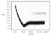
도 5는 입력 신호의 전력 레벨에 따라 발생되는 챠지 펌프의 전기적 특성을 나타내는 그래프이다.5 is a graph illustrating electrical characteristics of a charge pump generated according to a power level of an input signal.
도 5에 도시된 바와 같이, 입력 신호의 전력 레벨이 35dBm 이상인 경우 챠지 펌프에서 공급하던 -1.85V의 출력이 불안정해지는 것을 볼 수 있다.As shown in Figure 5, when the power level of the input signal is more than 35dBm it can be seen that the output of -1.85V supplied from the charge pump becomes unstable.
이를 위해, 본 발명의 RF 스위치 회로에 리미터가 채용될 수 있다.
For this purpose, a limiter may be employed in the RF switch circuit of the present invention.
도 6은 본 발명의 RF 스위치 회로에 채용된 리미터의 개략적인 구성도이다.6 is a schematic configuration diagram of a limiter employed in the RF switch circuit of the present invention.
도 6을 참조하면, 본 발명의 RF 스위치 회로에 채용된 리미터(130)는 딥 N형 웰 다이오드로 구성될 수 있으며, 도 1에도 도시된 바와 같이 상기 딥 N형 웰 다이오드의 캐소드는 제1 플로팅 저항(R1)과 제1 캐패시터(C1)이 각각 연결되고 제1 플로팅 저항(R1)과 제1 캐패시터(C1)은 접지(GND)에 연결될 수 있다. 상기 딥 N형 웰 다이오드의 애노드는 제2 플로팅 저항(R2)과 제2 캐패시터(C2)가 각각 연결되고, 제2 플로팅 저항(R2)은 구동 전원(Vdd)을 공급받고, 제2 캐패시터(C2)는 접지에 연결될 수 있다.
Referring to FIG. 6, the
도 7은 본 발명에 채용된 챠지 펌프의 전기적 특성을 나타내는 그래프이다.7 is a graph showing the electrical characteristics of the charge pump employed in the present invention.
도 7을 참조하면, 본 발명에 채용된 챠지 펌프는 입력 신호가 대신호의 레벨이 입력되어도 안정적으로 동작하는 것을 볼 수 있다.
Referring to FIG. 7, it can be seen that the charge pump employed in the present invention operates stably even when a large signal level is input.
도 8 내지 도 11은 본 발명의 RF 스위치 회로의 전기적 특성을 나타내는 그래프이다.8 to 11 are graphs showing electrical characteristics of the RF switch circuit of the present invention.
도 8 및 도 9에 도시된 바와 같이, 종래1 및 종래2에 대비하여 본 발명의 RF 스위치 회로는 삽입 손실과 차단성은 큰 변화가 없음을 나타낸다. 여기서 종래1은 RF 스위치만 플로팅 저항을 연결한 경우, 종래2는 RF 스위치와 스위치 컨트롤러에 플로팅 저항을 연결한 경우를 의미한다.
As shown in Figs. 8 and 9, the RF switch circuit of the present invention as compared with the conventional 1 and the conventional 2 shows that the insertion loss and the blocking property do not change significantly. Here, the conventional art 1 is a case where only the RF switch is connected to the floating resistor, the
반면, 도 10을 참조하면 종래2의 경우 입력 신호35dBm에서의 P1dB는 34dBm인 것을 볼 수 있으나, 도 11을 참조하면, 본 발명의 RF 스위치 회로는 입력 신호 35dBm에서도 P1dB가 포화되지 않고, 입력 신호가 38dBm에서도 P1dB는 37dBm을 달성하여 종래2에 대비하여 P1dB가 3dBm이나 증가한 것을 볼 수 있다.
On the other hand, referring to FIG. 10, in the
상술한 바와 같이, 본 발명에 따르면, RF 스위치 회로의 삽입 손실 및 차단성을 저해하지 않고도 기판을 통해 스위치 컨트롤러에 전달되는 입력 신호의 전력 레벨을 제어함으로써, 입력 신호의 레벨 범위를 확장시키고 대신호의 입력 신호에서도 안정적인 동작을 수행할 수 있다.
As described above, according to the present invention, by controlling the power level of the input signal transmitted to the switch controller through the substrate without compromising the insertion loss and blocking of the RF switch circuit, the range of the level of the input signal is extended and Stable operation can be performed on the input signal.
이상에서 설명한 본 발명은 전술한 실시예 및 첨부된 도면에 의해 한정되는 것이 아니고 후술하는 특허청구범위에 의해 한정되며, 본 발명의 구성은 본 발명의 기술적 사상을 벗어나지 않는 범위 내에서 그 구성을 다양하게 변경 및 개조할 수 있다는 것을 본 발명이 속하는 기술 분야에서 통상의 지식을 가진 자는 쉽게 알 수 있다.It is to be understood that both the foregoing general description and the following detailed description are exemplary and explanatory and are not intended to limit the invention to the particular forms disclosed. It will be understood by those skilled in the art that various changes in form and details may be made therein without departing from the spirit and scope of the invention as defined by the appended claims.
100..RF 스위치 회로110...RF 스위치
120...스위치 컨트롤러121...N MOS 스위치
122...P MOS 스위치130...리미터
120 ...
122 ...
Claims (8)
Translated fromKorean상기 칩 기판에 형성되어 상기 RF 스위치의 경로 변경을 제어하는 적어도 하나의 N MOS 스위치 및 P MOS 스위치를 구비하는 스위치 컨트롤러; 및
상기 칩 기판에 형성되어 상기 RF 스위치로부터 상기 스위치 컨트롤러에 전달되는 RF 신호의 레벨을 제한하는 딥(deep) N형 웰(well) 다이오드를 구비하는 리미터를 포함하며,
상기 RF 스위치의 N MOS 스위치는 플로팅(floating) 저항을 통해 해당하는 전원을 공급받고, 상기 스위치 컨트롤러의 적어도 하나의 N MOS 스위치 및 P MOS 스위치는 플로팅 저항을 통해 해당하는 전원을 공급받는 것을 특징으로 하는 RF 스위치 회로.An RF switch formed on one chip substrate and having at least one N metal oxide semiconductor (N MOS) switch configured to change a transmission path of an RF signal;
A switch controller formed on the chip substrate and having at least one N MOS switch and a P MOS switch for controlling a path change of the RF switch; And
A limiter formed on the chip substrate and having a deep N-type well diode for limiting the level of the RF signal transmitted from the RF switch to the switch controller,
The N MOS switch of the RF switch is supplied with a corresponding power supply through a floating resistor, and the at least one N MOS switch and the P MOS switch of the switch controller are supplied with a corresponding power supply through a floating resistor. RF switch circuit.
상기 RF 스위치의 N MOS 스위치는 칩 기판 상에 형성된 제1 딥(deep) N형 웰(well) 기판에 형성되어 플로팅(floating) 저항을 통해 구동 전원을 전달받는 N형 단자, 상기 제1 딥 N형 웰(well) 기판 상에 형성된 제1 P형 기판에 형성되어 플로팅 저항을 통해 바디 전원을 전달받는 P형 단자 및 플로팅 저항을 통해 게이트 전원을 전달받는 둘의 N형 단자를 갖는 것을 특징으로 하는 RF 스위치 회로.The method of claim 1,
The N-MOS switch of the RF switch is an N-type terminal formed on a first deep N-type well substrate formed on a chip substrate and receiving driving power through a floating resistor, and the first deep N And a P-type terminal formed on the first P-type substrate formed on the type well substrate and receiving the body power through the floating resistor, and two N-type terminals receiving the gate power through the floating resistor. RF switch circuit.
상기 스위치 컨트롤러의 N MOS 스위치는 상기 칩 기판 상에 형성된 제2 딥 N형 웰(well) 기판에 형성되어 플로팅(floating) 저항을 통해 구동 전원을 전달받는 N형 단자, 상기 제2 딥 N형 웰(well) 기판 상에 형성된 제2 P형 기판에 형성된 P형 단자 및 둘의 N형 단자를 갖고,
상기 스위치 컨트롤러의 P MOS 스위치는 상기 칩 기판 상에 형성된 제1 N형 기판에 형성된 둘의 P형 단자 및 플로팅(floating) 저항을 통해 구동 전원을 전달받는 N형 단자를 갖는 것을 특징으로 하는 RF 스위치 회로.The method of claim 2,
The N MOS switch of the switch controller is an N-type terminal formed on a second deep N-type well substrate formed on the chip substrate to receive driving power through a floating resistor, and the second deep N-type well. (well) having a P-type terminal and two N-type terminals formed on a second P-type substrate formed on the substrate,
The P MOS switch of the switch controller has an RF switch, characterized in that it has two P-type terminals formed on the first N-type substrate formed on the chip substrate and an N-type terminal receiving driving power through a floating resistor. Circuit.
상기 리미터의 딥 N형 웰 다이오드는 상기 칩 기판 상에 형성된 제3 딥 N형 웰(well) 기판에 형성되어 플로팅(floating) 저항을 통해 구동 전원을 전달받는 N형 단자, 상기 제3 딥 N형 웰(well) 기판 상에 형성된 제3 P형 기판에 형성되어 제1 플로팅 저항을 통해 접지에 연결되고 상기 제1 플로팅 저항에 병렬 연결되는 제1 캐패시터를 갖는 P형 단자 및 제2 플로팅 저항을 통해 구동 전원을 전달받고 상기 제2 플로팅 저항과 접지간에 연결된 제2 캐패시터를 갖는 N형 단자를 구비하는 RF 스위치 회로.The method of claim 3,
The deep N-type well diode of the limiter is an N-type terminal formed on a third deep N-type well substrate formed on the chip substrate to receive driving power through a floating resistor, and the third deep N-type P-type terminals having a first capacitor formed on a third P-type substrate formed on a well substrate and connected to ground through a first floating resistor and connected in parallel to the first floating resistor, and through a second floating resistor. And an n-type terminal having a second capacitor coupled to the second floating resistor and the ground, the drive power being received.
상기 스위치 컨트롤러는
기준 신호를 제공하는 발진기;
상기 발진기로부터의 기준 신호의 전압 레벨을 변환하는 챠지 펌프;
외부로부터의 제어 비트를 디코딩하는 디코더; 및
상기 디코더로부터의 디코딩된 신호에 따라 챠지 펌프에 의해 변환된 전압의 레벨을 쉬프트하여 상기 RF 스위치에 제공하는 레벨 시프터를 포함하되,
상기 발진기, 챠지 펌프, 디코더 및 레벨 쉬프터는 각각 상기 적어도 하나의 N MOS 스위치 및 P MOS 스위치를 구비하는 것을 특징으로 하는 RF 스위치 회로.The method of claim 3,
The switch controller
An oscillator providing a reference signal;
A charge pump for converting a voltage level of a reference signal from the oscillator;
A decoder for decoding control bits from the outside; And
A level shifter for shifting the level of the voltage converted by the charge pump according to the decoded signal from the decoder to provide the RF switch,
And said oscillator, charge pump, decoder and level shifter comprise said at least one N MOS switch and a P MOS switch, respectively.
상기 RF 스위치의 적어도 하나의 N MOS 스위치는 표준 CMOS 공정에 의한 N 채널 MOS FET(Field-Effect Transistor)인 것을 특징으로 하는 RF 스위치 회로.The method of claim 1,
At least one N MOS switch of the RF switch is an N-channel MOS Field-Effect Transistor (FET) by a standard CMOS process.
상기 스위치 컨트롤러의 적어도 하나의 N MOS 스위치 및 P MOS 스위치는 각각 표준 CMOS 공정에 의한 N 채널 MOS FET(Field-Effect Transistor) 및 P 채널 MOS FET(Field-Effect Transistor)인 것을 특징으로 하는 RF 스위치 회로.The method of claim 1,
The at least one N MOS switch and the P MOS switch of the switch controller are N-channel MOS (Field-Effect Transistor) and P-channel MOS (Field-Effect Transistor), respectively, by a standard CMOS process. .
상기 리미터의 딥 N형 웰 다이오드는 표준 CMOS 공정으로 형성되는 것을 특징으로 하는 RF 스위치 회로.The method of claim 1,
And the deep n-type well diode of the limiter is formed in a standard CMOS process.
Priority Applications (2)
| Application Number | Priority Date | Filing Date | Title |
|---|---|---|---|
| KR1020100009125AKR101153524B1 (en) | 2010-02-01 | 2010-02-01 | Radio frequency switch circuit |
| US13/016,499US8476959B2 (en) | 2010-02-01 | 2011-01-28 | Radio frequency switch circuit |
Applications Claiming Priority (1)
| Application Number | Priority Date | Filing Date | Title |
|---|---|---|---|
| KR1020100009125AKR101153524B1 (en) | 2010-02-01 | 2010-02-01 | Radio frequency switch circuit |
Publications (2)
| Publication Number | Publication Date |
|---|---|
| KR20110089636A KR20110089636A (en) | 2011-08-09 |
| KR101153524B1true KR101153524B1 (en) | 2012-06-12 |
Family
ID=44341099
Family Applications (1)
| Application Number | Title | Priority Date | Filing Date |
|---|---|---|---|
| KR1020100009125AExpired - Fee RelatedKR101153524B1 (en) | 2010-02-01 | 2010-02-01 | Radio frequency switch circuit |
Country Status (2)
| Country | Link |
|---|---|
| US (1) | US8476959B2 (en) |
| KR (1) | KR101153524B1 (en) |
Families Citing this family (8)
| Publication number | Priority date | Publication date | Assignee | Title |
|---|---|---|---|---|
| US9111767B2 (en) | 2012-06-29 | 2015-08-18 | Freescale Semiconductor, Inc. | Semiconductor device and driver circuit with source and isolation structure interconnected through a diode circuit, and method of manufacture thereof |
| US20140001546A1 (en)* | 2012-06-29 | 2014-01-02 | Hubert M. Bode | Semiconductor device and driver circuit with a current carrying region and isolation structure interconnected through a resistor circuit, and method of manufacture thereof |
| US9142554B2 (en) | 2012-06-29 | 2015-09-22 | Freescale Semiconductor, Inc. | Semiconductor device and driver circuit with an active device and isolation structure interconnected through a diode circuit, and method of manufacture thereof |
| US9129990B2 (en) | 2012-06-29 | 2015-09-08 | Freescale Semiconductor, Inc. | Semiconductor device and driver circuit with drain and isolation structure interconnected through a diode circuit, and method of manufacture thereof |
| JP6156841B2 (en)* | 2012-11-07 | 2017-07-05 | エヌエックスピー ユーエスエイ インコーポレイテッドNXP USA,Inc. | SEMICONDUCTOR DEVICE AND DRIVER CIRCUIT HAVING ACTIVE DEVICE AND ISOLATED STRUCTURE INTERCONNECTED THROUGH RESISTANCE CIRCUIT AND ITS MANUFACTURING METHOD |
| JP6034268B2 (en)* | 2013-09-13 | 2016-11-30 | 株式会社東芝 | Semiconductor device |
| US10854596B2 (en)* | 2018-11-29 | 2020-12-01 | Berex, Inc. | CMOS RF power limiter and ESD protection circuits |
| TWI747292B (en)* | 2019-07-12 | 2021-11-21 | 台灣積體電路製造股份有限公司 | Semiconductor device |
Citations (2)
| Publication number | Priority date | Publication date | Assignee | Title |
|---|---|---|---|---|
| JPH0282570A (en)* | 1988-09-19 | 1990-03-23 | Nec Corp | semiconductor equipment |
| KR20010021489A (en)* | 1997-10-27 | 2001-03-15 | 가네꼬 히사시 | Semiconductor integrated circuit |
Family Cites Families (7)
| Publication number | Priority date | Publication date | Assignee | Title |
|---|---|---|---|---|
| US5818099A (en)* | 1996-10-03 | 1998-10-06 | International Business Machines Corporation | MOS high frequency switch circuit using a variable well bias |
| JP2964975B2 (en)* | 1997-02-26 | 1999-10-18 | 日本電気株式会社 | High frequency switch circuit |
| EP1498998A1 (en)* | 2003-07-16 | 2005-01-19 | Dialog Semiconductor GmbH | Protection switch with reverse voltage protection |
| US7890063B2 (en)* | 2006-10-03 | 2011-02-15 | Samsung Electro-Mechanics | Systems, methods, and apparatuses for complementary metal oxide semiconductor (CMOS) antenna switches using body switching in multistacking structure |
| US7843280B2 (en) | 2006-12-01 | 2010-11-30 | Samsung Electro-Mechanics Company | Systems, methods, and apparatuses for high power complementary metal oxide semiconductor (CMOS) antenna switches using body switching and substrate junction diode controlling in multistacking structure |
| US7848712B2 (en) | 2007-05-03 | 2010-12-07 | Intel Corporation | CMOS RF switch for high-performance radio systems |
| US8058922B2 (en)* | 2009-07-28 | 2011-11-15 | Qualcomm, Incorporated | Switch with improved biasing |
- 2010
- 2010-02-01KRKR1020100009125Apatent/KR101153524B1/ennot_activeExpired - Fee Related
- 2011
- 2011-01-28USUS13/016,499patent/US8476959B2/ennot_activeExpired - Fee Related
Patent Citations (2)
| Publication number | Priority date | Publication date | Assignee | Title |
|---|---|---|---|---|
| JPH0282570A (en)* | 1988-09-19 | 1990-03-23 | Nec Corp | semiconductor equipment |
| KR20010021489A (en)* | 1997-10-27 | 2001-03-15 | 가네꼬 히사시 | Semiconductor integrated circuit |
Also Published As
| Publication number | Publication date |
|---|---|
| KR20110089636A (en) | 2011-08-09 |
| US20110187475A1 (en) | 2011-08-04 |
| US8476959B2 (en) | 2013-07-02 |
Similar Documents
| Publication | Publication Date | Title |
|---|---|---|
| KR101153524B1 (en) | Radio frequency switch circuit | |
| TWI675551B (en) | Body-biased switching device | |
| US7408399B2 (en) | Active driving of normally on, normally off cascoded configuration devices through asymmetrical CMOS | |
| US8295784B2 (en) | Semiconductor switching device | |
| US20110050288A1 (en) | Semiconductor switch | |
| US9525410B2 (en) | Power management chips and power management devices including the same | |
| US8461911B2 (en) | Semiconductor switch for switching terminals | |
| US8884650B2 (en) | High-frequency semiconductor switching circuit | |
| US9020448B2 (en) | Switch control circuit, semiconductor device, and radio communication device | |
| US8497726B2 (en) | Level shifter | |
| KR101153565B1 (en) | Radio frequency switch circuit | |
| US9264045B2 (en) | Buffer circuit with reduced static leakage through controlled body biasing in FDSOI technology | |
| CN215897704U (en) | Radio frequency switching circuit and multi-stage buffer | |
| JP5366911B2 (en) | High frequency switch circuit | |
| US8476956B2 (en) | Semiconductor switch | |
| KR101101465B1 (en) | Raf switch controller | |
| JP5450955B2 (en) | High frequency switch | |
| US6713815B2 (en) | Semiconductor device with transistors that convert a voltage difference into a drain current difference | |
| JP2010278110A (en) | Semiconductor device and high-frequency switch circuit | |
| JP5114226B2 (en) | Semiconductor switch circuit | |
| CN115940595B (en) | Output drive circuit for power module and drive circuit system using the same | |
| TWI802096B (en) | Transistor device | |
| US9590575B2 (en) | Amplifier stage | |
| JP2013229647A (en) | Semiconductor switch circuit |
Legal Events
| Date | Code | Title | Description |
|---|---|---|---|
| A201 | Request for examination | ||
| PA0109 | Patent application | St.27 status event code:A-0-1-A10-A12-nap-PA0109 | |
| PA0201 | Request for examination | St.27 status event code:A-1-2-D10-D11-exm-PA0201 | |
| D13-X000 | Search requested | St.27 status event code:A-1-2-D10-D13-srh-X000 | |
| D14-X000 | Search report completed | St.27 status event code:A-1-2-D10-D14-srh-X000 | |
| PG1501 | Laying open of application | St.27 status event code:A-1-1-Q10-Q12-nap-PG1501 | |
| PE0902 | Notice of grounds for rejection | St.27 status event code:A-1-2-D10-D21-exm-PE0902 | |
| T11-X000 | Administrative time limit extension requested | St.27 status event code:U-3-3-T10-T11-oth-X000 | |
| E701 | Decision to grant or registration of patent right | ||
| PE0701 | Decision of registration | St.27 status event code:A-1-2-D10-D22-exm-PE0701 | |
| GRNT | Written decision to grant | ||
| PR0701 | Registration of establishment | St.27 status event code:A-2-4-F10-F11-exm-PR0701 | |
| PR1002 | Payment of registration fee | St.27 status event code:A-2-2-U10-U11-oth-PR1002 Fee payment year number:1 | |
| PG1601 | Publication of registration | St.27 status event code:A-4-4-Q10-Q13-nap-PG1601 | |
| R18-X000 | Changes to party contact information recorded | St.27 status event code:A-5-5-R10-R18-oth-X000 | |
| R18-X000 | Changes to party contact information recorded | St.27 status event code:A-5-5-R10-R18-oth-X000 | |
| PN2301 | Change of applicant | St.27 status event code:A-5-5-R10-R13-asn-PN2301 St.27 status event code:A-5-5-R10-R11-asn-PN2301 | |
| R18-X000 | Changes to party contact information recorded | St.27 status event code:A-5-5-R10-R18-oth-X000 | |
| PR1001 | Payment of annual fee | St.27 status event code:A-4-4-U10-U11-oth-PR1001 Fee payment year number:4 | |
| PR1001 | Payment of annual fee | St.27 status event code:A-4-4-U10-U11-oth-PR1001 Fee payment year number:5 | |
| FPAY | Annual fee payment | Payment date:20170102 Year of fee payment:6 | |
| PR1001 | Payment of annual fee | St.27 status event code:A-4-4-U10-U11-oth-PR1001 Fee payment year number:6 | |
| FPAY | Annual fee payment | Payment date:20180403 Year of fee payment:7 | |
| PR1001 | Payment of annual fee | St.27 status event code:A-4-4-U10-U11-oth-PR1001 Fee payment year number:7 | |
| FPAY | Annual fee payment | Payment date:20190401 Year of fee payment:8 | |
| PR1001 | Payment of annual fee | St.27 status event code:A-4-4-U10-U11-oth-PR1001 Fee payment year number:8 | |
| R18-X000 | Changes to party contact information recorded | St.27 status event code:A-5-5-R10-R18-oth-X000 | |
| R18-X000 | Changes to party contact information recorded | St.27 status event code:A-5-5-R10-R18-oth-X000 | |
| PR1001 | Payment of annual fee | St.27 status event code:A-4-4-U10-U11-oth-PR1001 Fee payment year number:9 | |
| PN2301 | Change of applicant | St.27 status event code:A-5-5-R10-R13-asn-PN2301 St.27 status event code:A-5-5-R10-R11-asn-PN2301 | |
| R18-X000 | Changes to party contact information recorded | St.27 status event code:A-5-5-R10-R18-oth-X000 | |
| PR1001 | Payment of annual fee | St.27 status event code:A-4-4-U10-U11-oth-PR1001 Fee payment year number:10 | |
| PR1001 | Payment of annual fee | St.27 status event code:A-4-4-U10-U11-oth-PR1001 Fee payment year number:11 | |
| R18-X000 | Changes to party contact information recorded | St.27 status event code:A-5-5-R10-R18-oth-X000 | |
| PR1001 | Payment of annual fee | St.27 status event code:A-4-4-U10-U11-oth-PR1001 Fee payment year number:12 | |
| R18-X000 | Changes to party contact information recorded | St.27 status event code:A-5-5-R10-R18-oth-X000 | |
| PC1903 | Unpaid annual fee | St.27 status event code:A-4-4-U10-U13-oth-PC1903 Not in force date:20240531 Payment event data comment text:Termination Category : DEFAULT_OF_REGISTRATION_FEE | |
| PC1903 | Unpaid annual fee | St.27 status event code:N-4-6-H10-H13-oth-PC1903 Ip right cessation event data comment text:Termination Category : DEFAULT_OF_REGISTRATION_FEE Not in force date:20240531 |